modeling of dynamic behavior of printed circuit...
TRANSCRIPT

MODELING OF DYNAMIC BEHAVIOR OF PRINTED CIRCUIT BOARD
(PCB) SUBJECTED TO MECHANICAL SHOCK LOADING
LAU CHIN WEI
A dissertation submitted in partial fulfilment of the
requirements for the degree of Master of Engineering
in Mechanical Engineering
Faculty of Mechanical Engineering
Universiti Teknologi Malaysia
MAY, 2006

iii
Dedicated to my country,
And
To my beloved father, mother and brothers.
iv
ACKNOWLEDGEMENT
Praises to God for giving me the patience, strength and will to go through and
complete my study. I would like to express my deepest gratitude to my supervisor,
Dr. Nazri Kamsah for his generous guidance, cooperation and advices from time to
time throughout the duration of this dissertation. His valuable knowledge and support
is greatly appreciated.
My sincere appreciation also extends to my laboratory mate, Mr. Liew Yik
Ban and my team mate, Mr. Vijay Anand Ramadass for their patient guidance on
using the ABAQUS finite element software and knowledge sharing. My recognition
also extends to Assoc. Professor Dr. Mohd Nasir Tamin, Professor Dr. Roslan Abdul
Rahman and Assoc. Professor Dr. Abdullah Idris for their kind guidance and sharing
the knowledge on certain technical aspects of this dissertation. Besides, I would like
to express my appreciation to the Vibration Laboratory technician, Mr. Elfendy for
his technical support.
Special thanks go to my friends, Goh Hock Ann, Opong and Lee Yuk Choi
for always giving me their utmost encouragement and moral support.
Last but not least, I would like to thank my family and all my friends for
giving their cheering supports.
v
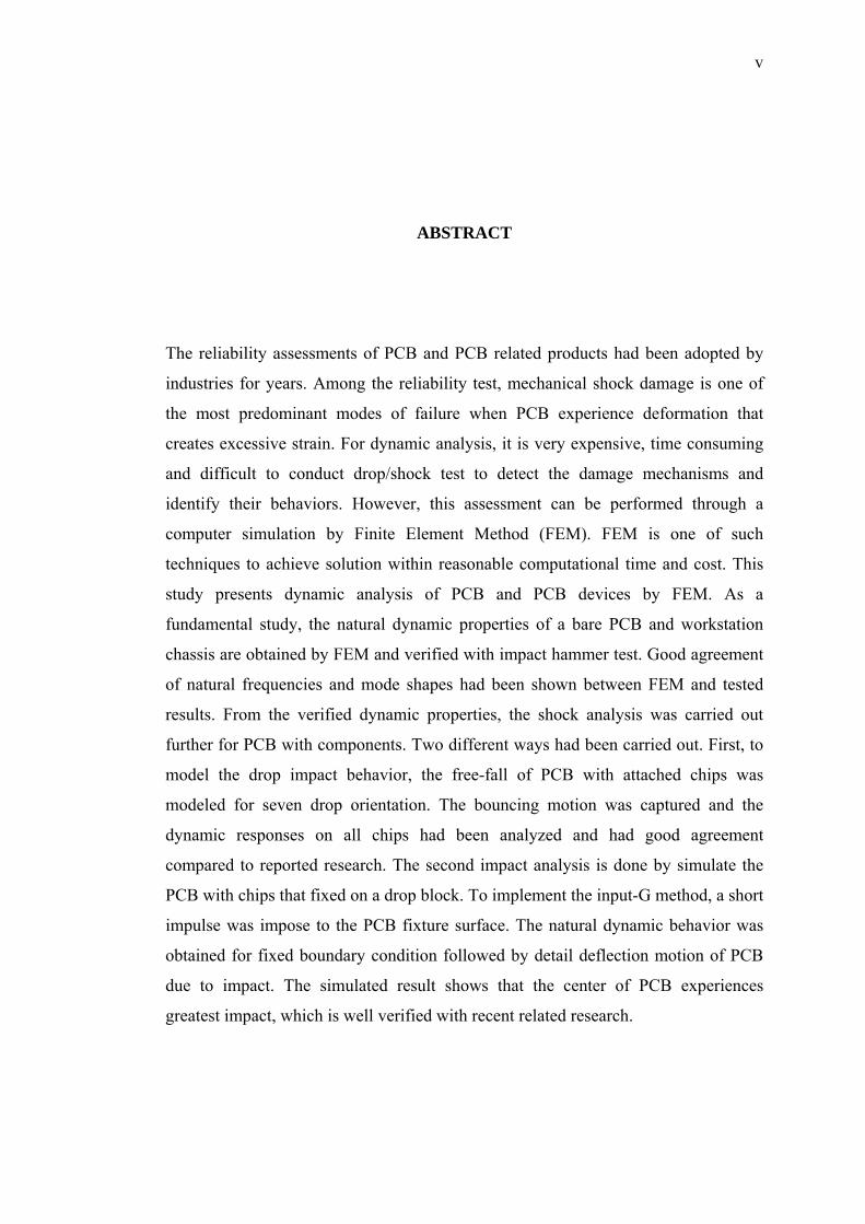
ABSTRACT
The reliability assessments of PCB and PCB related products had been adopted by
industries for years. Among the reliability test, mechanical shock damage is one of
the most predominant modes of failure when PCB experience deformation that
creates excessive strain. For dynamic analysis, it is very expensive, time consuming
and difficult to conduct drop/shock test to detect the damage mechanisms and
identify their behaviors. However, this assessment can be performed through a
computer simulation by Finite Element Method (FEM). FEM is one of such
techniques to achieve solution within reasonable computational time and cost. This
study presents dynamic analysis of PCB and PCB devices by FEM. As a
fundamental study, the natural dynamic properties of a bare PCB and workstation
chassis are obtained by FEM and verified with impact hammer test. Good agreement
of natural frequencies and mode shapes had been shown between FEM and tested
results. From the verified dynamic properties, the shock analysis was carried out
further for PCB with components. Two different ways had been carried out. First, to
model the drop impact behavior, the free-fall of PCB with attached chips was
modeled for seven drop orientation. The bouncing motion was captured and the
dynamic responses on all chips had been analyzed and had good agreement
compared to reported research. The second impact analysis is done by simulate the
PCB with chips that fixed on a drop block. To implement the input-G method, a short
impulse was impose to the PCB fixture surface. The natural dynamic behavior was
obtained for fixed boundary condition followed by detail deflection motion of PCB
due to impact. The simulated result shows that the center of PCB experiences
greatest impact, which is well verified with recent related research.

vi
ABSTRAK
Pengukuran kebolehtahanan papan litar cetak (PCB) dan produk berkaitan telah lama
diamalkan dalam industri. Antaranya, kerosakan kejutan mekanikal merupakan salah
satu mod pradominan yang menyebabkan kerosakan pada PCB akibat terikan hasil
daripada lenturan. Untuk analisa dinamik, adalah mahal, makan masa dan susah
untuk menjalankan ujikaji bagi mengesan mekanisma kerosakan dan mengenali
kelakuannya. Namun, pengukuran ini dapat dijalankan dengan simulasi komputer
melalui Kaedah Unsur Terhingga (FEM). Ia merupakan salah satu teknik
penyelesaian yang menggunakan perbelanjaan dan masa yang berpatutan. Kajian ini
mempersembahkan analisa dinamik PCB melalui FEM. Sebagai kajian dasar, sifat
getaran semulajadi pada PCB dan rangkanya telah dikaji dan disahkan dengan ujikaji
hentaman tukul. Keputusan antara FEM dan ujikaji didapati bersetuju. Daripada
keputusan tersebut, analisa kejutan dibuat dengan PCB berkomponen. Dua cara telah
diperkenalkan. Pertamanya, untuk mengkaji kejutan jatuh, PCB berkomponen telah
dimodel jatuh bebas pada tujuh arah yang berlainan. Pergerakan lonjakan dan tindak
laku dinamik telah diperoleh dan setuju dengan perbandingan kajian lain. Cara kedua
disimulasi dengan PCB berkomponen yang ditempatkan pada blok jatuh. Untuk
mengimplikasi cara kemasukan-G, kejutan pantas telah dikenakan pada permukaan
ikatan PCB. Sifat getaran semulajadi telah diperolehi bagi keadaan terikat dan
seterusnya pergerakan lenturan PCB akibat daripada kejutan. Keputusan simulasi
menunjukkan bahawa bahagian tengah PCB mengalami lenturan yang paling ketara,
di mana pendapatan ini adalah bersetuju dengan kajian-kajian baru yang berkaitan.
vii
TABLE OF CONTENTS
CHAPTER TOPIC
PAGE
TITLE i
DECLARATION ii
DEDICATION iii
ACKNOWLEDGEMENT iv
ABSTRACT v
ABSTRAK vi
TABLE OF CONTENTS vii
LIST OF TABLES x
LIST OF FIGURES xi
GENERAL NOTATIONS xiv
CHAPTER 1 INTRODUCTION 1
1.1 Introduction 1
1.2 Prior Research On Mechanical Vibration and Impact 4
1.3 Objectives of the Project 7
1.4 Scopes of the Project 7
CHAPTER 2 LITERATURE REVIEW 8
2.1 Material Science of Printed Circuit Board 8
2.1.1 PCB Construction 9
2.1.2 Base Material 10

viii
2.1.3 Desktop Motherboard 12
2.2 Mechanics of Composite Materials 13
2.3 Plate Theory 16
2.3.1 Thin Plate Theory 17
2.3.2 Boundary Condition Governing Equations 20
2.4 Vibration Test 22
2.4.1 Excitation Technique 22
2.4.2 System Assumptions 23
2.4.3 Excitation Assumptions 24
2.5 Boundary Condition 25
2.5.1 Free Boundary Condition 26
2.5.2 Grounded Boundary Condition 27
2.5.3 Comparison of varies boundary condition 27
2.6 Drop/Impact Test Method 28
2.6.1 General Free Fall Test Method 29
CHAPTER 3 METHODOLOGY 34
3.1 Vibration Testing 36
3.1.1 PCB Hammer Impact Test 36 3.1.2 Chassis Hammer Impact Test 37
3.2 Computational Modeling and Simulation 40
3.2.1 ABAQUS 41
3.2.2 Pre-processing Procedure 42
3.2.3 Modeling of the Geometry 43
3.2.4 Specification of Material Property 43
3.2.5 Analysis Step 45
3.2.6 Specification of Boundary and Loading Condition 46
3.2.7 Meshing 46
ix
3.3 Chassis vibration simulation 40
3.3.1 Part 47
3.3.2 Material 49
3.4 Impact analysis simulation 51
3.4.1 PCB drop 51
3.4.2 PCB impact 52
CHAPTER 4 VIBRATION ANALYSIS
4.1 PCB vibration 54
4.2 Chassis vibration 60
CHAPTER 5 DROP AND IMPACT ANALYSIS
5.1 PCB drop (Case 1-7) 68
5.2 PCB impact 99
5.2.1 Vibration with fixed boundary condition 99
5.2.2 Impact at 4 pinned points 103
CHAPTER 6 CONCLUSIONS AND SUGGESTIONS
6.1 Conclusions 107
6.2 Suggestions 108
REFERENCES 109-112
x
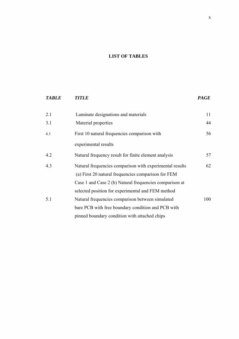
LIST OF TABLES
TABLE TITLE PAGE
2.1 Laminate designations and materials 11
3.1 Material properties 44
4.1 First 10 natural frequencies comparison with 56
experimental results
4.2 Natural frequency result for finite element analysis 57
4.3 Natural frequencies comparison with experimental results 62
(a) First 20 natural frequencies comparison for FEM
Case 1 and Case 2 (b) Natural frequencies comparison at
selected position for experimental and FEM method
5.1 Natural frequencies comparison between simulated 100
bare PCB with free boundary condition and PCB with
pinned boundary condition with attached chips

xi
LIST OF FIGURES
FIGURE TITLE PAGE
1.1 Critical solder ball and failure interface 2
1.2 PCB warpage distributions during maximum bending 2
1.3 PCB impact failure and related further studies 3
2.1 FCBGA Package 9
2.2 Nominal Board Stack Up 10
2.3 An ATX motherboard 12
2.4 Stress reference coordinates 14
2.5 Plate Geometry 17
2.6 CPT cross-sectional assumption 17
2.7 Resultant Forces in Plate 19
2.8 Plates with fully clamped edges and fully free edges 20
2.9 Hammer excitation 22
2.10 Shaker excitation 23
2.11 Setup for board-level tester 30
2.12 Setup for board-level tester with a special designed jig 30
2.13 Schematic diagrams showing different orientations for both 31
methods
3.1 Flow chart of overall problem solving method 36
3.2 Vibration testing set up for Impact/Hammer Test 37
3.3 Basic Step needed for FEM simulation 41
3.4 ABAQUS analysis step 42
3.5 Simplified motherboard model 43
3.6 Material orientation 45
3.7 Specified analysis step 46

xii
3.8 Plate meshing 47
3.9 Chassis as a whole part 48
3.10 Assembly parts of chassis 48
3.11 ‘Tie’ connections 49
3.12 Chassis in assembled condition 49
3.13 Iron base material 50
3.14 Zink coated material 50
3.15 Chips layout and PCB position for free-fall 51
3.16 Fixed PCB with applied transient force 52
3.17 Applied transient force in trapezium shape 53
4.1 Bare PCB acceleration responses in frequency domain 55
4.2 Comparison between experimental and FEM results 56
4.3 Mode shapes of bare PCB free vibration by 58
ABAQUS simulation
4.4 Mode shapes of free vibration 59
4.5 Chassis acceleration responses in frequency domain 60
(a) Resonance at side plate (b) Resonance at bottom plate
4.6 Selected FEM results for chassis natural frequencies 61
comparison (a)Resonance at bottom plate (b)Resonance at
side plate
4.7 Comparison between FEM Case 1 and FEM Case 2 results 63
4.8 The first 20 mode shapes of the chassis. 67
5.1 Case 1 PCB drop orientation with 5 concentrated masses 69
5.2 First 6 motions captured after free fall (a) to (f) 70
5.3 Energy results versus time 71
5.4 Acceleration histories of five chips on PCB 72
5.5 Velocity histories of five chips on PCB 72
5.6 Case 2 PCB drop orientation with 5 concentrated masses 73
5.7 First 6 motions captured after free fall (a) to (f) 74
5.8 Energy results versus time 75
5.9 Acceleration histories of five chips on PCB 76
5.10 Velocity histories of five chips on PCB 76
5.11 Case 3 PCB drop orientation with 5 concentrated masses 77

xiii
5.12 First 6 motions captured after free fall (a) to (f) 78
5.13 Energy results versus time 79
5.14 Acceleration histories of five chips on PCB 80
5.15 Velocity histories of five chips on PCB 80
5.16 Case 4 PCB drop orientation with 5 concentrated masses 81
5.17 First 6 motions captured after free fall (a) to (f) 82
5.18 Energy results versus time 83
5.19 Acceleration histories of five chips on PCB 84
5.20 Velocity histories of five chips on PCB 84
5.21 Case 5 PCB drop orientation with 5 concentrated masses 85
5.22 First 8 motions captured after free fall (a) to (h) 86
5.23 Energy results versus time 87
5.24 Acceleration histories of five chips on PCB 88
5.25 Velocity histories of five chips on PCB 89
5.26 Case 6 PCB drop orientation with 5 concentrated masses 89
5.27 First 12 motions captured after free fall (a) to (l) 91
5.28 Energy results versus time 92
5.29 Acceleration histories of five chips on PCB 93
5.30 Velocity histories of five chips on PCB 94
5.31 Case 7 PCB drop orientation with 5 concentrated masses 94
5.32 First 12 motions captured after free fall (a) to (l) 96
5.33 Energy results versus time 97
5.34 Acceleration histories of five chips on PCB 98
5.35 Velocity histories of five chips on PCB 99
5.36 Natural frequencies comparison between simulated 100
bare PCB with free boundary condition and PCB with
pinned boundary condition with attached chips
5.37 First 10 natural mode shapes of PCB for pinned 102
boundary condition and with attached chips
5.38 First 10 motions captured during and after impact (a) to (j) 105
5.39 Acceleration histories of five chips on PCB 105
5.40 Velocity histories of five chips on PCB 106
5.41 Deflection histories of five chips on PCB 106

xiv
GENERAL NOTATIONS
English Symbols
a - Length
b - Width
E - Young’s modulus
f - Force
G - Shear modulus
G(t) - Acceleration at time t
Gm - Peak acceleration or maximum shock level
g - Gravitational acceleration
H - Drop height
h - Thickness
k - Spring constant
L - Length
M - Moment
m - Mass
M - Bending Moments
S - Compliance Components
T - Impact duration
t - Time
x - Displacement
x& - Velocity
x&& - Acceleration

xv
Greek Symbols
υ - Poisson ratio
ρ - Density
ε - Strain
σ - Stress
λ - Wavelength
ω - Frequency
η - = y/b, dimensionless plate spatial coordinate
ξ - Damping ratio, or = x/a, dimensionless plate spatial coordinate
Abbreviations
CPU - Central Processing Unit
DOF - Degree of Freedom
FCBGA - Flip Chip Ball Grid Array
FE - Finite Element
FEM - Finite Element Method
FR - Flame Retardant
FRF - Frequency Response Function
FFT - Fast Fourier Transform
PBGA - Plastic Ball Grid Array
PCB - Printed Circuit Board
PCBA - Printed Circuit Board Assembly
SDOF - Single Degree of Freedom
SMT - Surface Mounting Technology

CHAPTER 1
INTRODUCTION
1.1 Introduction and Problem Definition
PCB is one of the major mechanical elements in most modern electronic systems.
Transportation and handling of PCBs and PCB related products may generate shock and
vibration on it. As a result, the PCB will experience deformation that creates excessive
strain, which is eventually leaded to failure.
Although portable devices such as PDA or mobile phone are the products which
were easily damage due to drop impact, this mechanical destruction is also the main
damage factor for non-portable products such as motherboard package of desktop
computer. Mishandling during transportation or customer usage may terribly damage the
package.
In the microscopic of view, the PCB experiences deflection during drop impact.
The PCB bending and mechanical shock will create extreme peeling stress (Figure 1.1,
1.2) that cracks the solder joints of electronic components that mounted on the PCB.
Both Tee et al., (2004) and Yang et al., (2000) had shown the results that the critical
stress always occur at the outer row or corner solder balls. The disconnection of
electronic circuit leads to malfunction of the product. Due to environmental protection

2
concerns, the usage of lead-free solders instead of lead-containing solders had results
more critical phenomenon because the higher moduli have more brittle mechanical
responses (Yeh and Lai, 2000). Although, conventionally, board-level reliability usually
refers to solder joint fatigue strength during the thermal cycling test (Tee et al., 2004) .
Figure 1.1 Critical solder ball and failure interface (Tee et al., (2004))
Figure 1.2 PCB warpage distributions during maximum bending (Tee et al., (2004))

3
Generally, PCB impact failure can be dividing into two fields: thermal impact and
dynamic impact as Figure 1.3. The dynamic impact is part of structural dynamic field
which concerns dynamic parameters such as deflection, velocity and acceleration of the
whole structure. The study then can be furthered by stress, strain analysis under fracture
mechanic analysis. Come to the last, the main reason of the study is to predict life of the
product followed by product improvement which is the main concern for manufacturers
in cost reduction and to benefit end users.
Figure 1.3 PCB impact failure and related further studies

4
1.2 Prior Research On Mechanical Vibration and Impact
It has always been a challenge to predict dynamic behavior of mechanical impact
for PCB and related devices. Since 1980, with the blow up of PCB related products, the
manufacturers are suffering from reliability of those products that may damage during
handling and transportation. On the other hand, the end users are demanding for more
robust products.
It was a difficult study to predict the final impact response on the product, even
more difficult is to catch what actually happened inside the product during shock or drop
that occur just within few milliseconds. In recent years, various impact predictions have
been proposed to capture the dynamic behavior of the products.
Most researchers agree that board-level test is much easier to conduct and
evaluate compare to the product-level test due to the complexity. Although there are
numbers of studies have been done on board-level evaluation, only a few have done for
product-level by simulation. However, it was a pre-requirement to study the board-level
structural dynamic before furthering in product-level analysis if the result are frequency
related data.
The investigations of vibration are presented as follows:
Wu et al., (2002) had presents vibration analysis of PCB by FEA model and
verified with the tested result. The simulation result had a close prediction to the tested
data within 7% error range. Yang et al., (2000) investigated dynamic properties of
PBGA assemblies using experimental modal testing and FE analysis. Bare PCB and
PCB assembly with PBGA modules mounted were tested and analyzed separately. The
dynamic investigation was limited to free and force vibration. Geng et al., (2003)
evaluated solder joint shock reliability for Intel’s desktop motherboard. Modal analysis
was introduced to evaluate and calibrate the test board fundamental frequency. An
external mass was mounted to the PCB to adjust the bare PCB behavior to the desktop
system level. The FEM analysis validation had shown good agreement with the tested
5
data. However, the shock testing and simulation were not included in this work. It
provides only as a ground work for shock test evaluation. Chen and Lue, (2005) had
study the free vibration characteristic of cross-ply laminated plates with a semi-
analytical method. The result had been verified by comparing the present data with the
exact elasticity solution for a simply supported plate. Allemang, (1983) had a detail
discussion on the experimental modal analysis method, into four categories: forced
normal mode excitation method, frequency response function method, damped complex
exponential function method and mathematical input-output model method.
While the investigations of shock/impact are presented as follows:
Tee et al., (2004) predict impact life by studying PCB bending and mechanical
shock. The drop test had been carried out and compare with explicit solver simulation.
Detail study such as effect of component position, drop orientation and boundary
condition of PCB had been evaluated. The quantitative approach provides both accurate
relative and absolute impact life prediction. Wang et al., (2004) carried out drop test
FEM simulation, especially the methodology for analyzing the reliability of electronic
devices under drop and impact. The structure with high complexity such as TV set
packaging and Aluminum casing had been simulate with same method. Yeh and Lai,
(2000) used the support excitation scheme in stead of the conventional drop test, in order
to omit drop table modeling and contact methodologies. For experimental work, JEDEC
drop test had been carried out. Both FEM and numerical studies had been done. The
comparison for different drop orientation had been done in detail. Wang et al., (2006)
modeled and simulated the drop-impact analysis of PCB. The experimental study was
carried out by actual drop test, where the images of specimen movements were capture
with a high-speed camera. Detail study had been done using FEA simulation for four
different models: isotropic, orthotropic, multi-layer uni-directional fiber and multi-layer
fill-warp PCB models. Allen and Bogy, (1996) studied the effects of shock on hard disk
drive by comparing drop test result from high speed camera with FEM modeling. The
comparison of both method shown discrepancy due to the linear and non-linear
conditions of simulation and testing, respectively. Ong et al., (2003) had studied drop
impact for both product-level and board-level of the Nokia Model 3210 mobile phone

6
and its PCB. The mechanical responses were obtained by a load cell, accelerometers and
strain gauges. The method was purely experimental, and several drop direction had been
done to study the relationship between mechanical responds and drop direction. Suhir,
(2002) had studied whether the shock tests could adequately replace drop tests. The
analytical result shows that in order to mimic the actual drop test, the shock test loading
should be as close as possible to an instantaneous impulse, and the duration of the shock
load should be established base on the lowest (fundamental) natural frequency of
vibrations.
1.3 Objectives Of The Project
The project is concerned with modeling of dynamic behavior of PCB subjected
to mechanical shock loading. The objectives are as follows:
1) To understand current experimental method of mechanical shock tested on PCB
(board-level) and PCB with chassis (product-level).
2) To simplify actual condition of product-level PCB and perform simulation
modeling to obtain PCB dynamic responses due to free-fall and input-G.
1.4 Scopes of The Project
The scopes of project are as follows:
1) Undertake the FEM modeling of a PCB at simplified board-level condition.
2) Carry out further modeling study with isotropic and orthotropic model.
3) Conduct parametric study with the best model to investigate PCB response under
effect of other features.
7
4) For verification, mechanical shock test of simplified product-level PCB should
be performed either stimulating external impact on a static PCB or free-fall of
PCB itself.
The remainder of the report is organized as follows. In Chapter 2, the theory of
PCB structure, structural dynamic background, vibration test and conventional drop test
is elaborated for better understanding of the solution method. In Chapter 3, the method
of solution is introduced for vibration and shock/impact evaluation, for both
experimental and FEM simulation method. Chapter 4 shows the results of PCB and
chassis vibration analysis. Chapter 5 discussed the free-fall and input-G results for PCB
with chips. In Chapter 6, conclusions of the research are presented with summary on
major findings in the study. Future works for refining the research are recommended.