modeling of the architectural studies for the panda dat system k. korcyl 1,2 w. kuehn 3, j....
TRANSCRIPT
Modeling of the architectural studies for the PANDA DAT system
K. Korcyl1,2
W. Kuehn3, J. Otwinowski1, P. Salabura1, L. Schmitt4
1Jagiellonian University,Krakow, Poland 2Cracow University of Technology, Krakow, Poland
3Justus-Liebig Universitat Giessen, Giessen, Germany4GSI, Darmstadt, Germany
Outline
The PANDA experiment and TDAQ system Architecture proposal and operation of basic
components Detector Concentrator Board organization L1 processing node
Model of the architecture Preliminary results
Conclusions
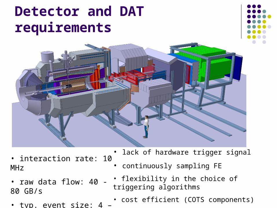
Detector and DAT requirements
• interaction rate: 10 MHz
• raw data flow: 40 - 80 GB/s
• typ. event size: 4 – 8 kB
• lack of hardware trigger signal
• continuously sampling FE
• flexibility in the choice of triggering algorithms
• cost efficient (COTS components)
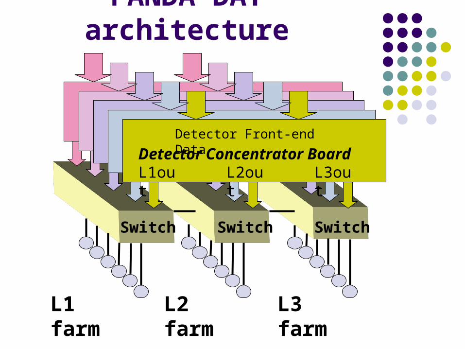
Detector Concentrator Board
Switch
L1 farm
L1out
Detector Front-end Data
PANDA DAT architecture
L2out L3out
Switch Switch
L2 farm L3 farm

Detector Front End Electronics
Receives precise synchronous clock signal from the central distribution system
Continuously sampling mode of operation capable of autonomous hit detection
Time stamps data with the interaction time based on the central clock and expedites message towards the DCB
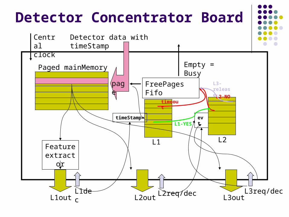
Detector Concentrator Board
FreePages Fifo
Detector data with timeStamp
Paged mainMemory
timeStamp
Feature extractor
L1out L2out L3out
evt
page
L1 L2
L1dec L2req/dec L3req/dec
Empty = Busy
Central clock
timeoutL2-NO
L1-YES
L3-release
Detector Concentrator Board (2)
Local filtering process (Feature Extraction) is started with DCB_INSPECT_LATENCY. It may result in generation of a message to the LVL1 farm.
The L1 structure is cleared by the purge process running with the DCB_PURGE_LATENCY and the TIME STAMP rate. Addresses of pages found in the L1 at position DCB_PURGE_LATENCY are returned back to the free pages fifo (detector data will be overwritten).
Positive LVL1 decisions save detector data, by moving the page address from the L1 to the L2 structure
Detector Concentrator Board (3)
The DCB uses the TIME STAMPs to calculate address of the LVL1 processing node to send the features to.
N concecutive TIME STAMPs are directed to the same L1port. neutralizes quantization of time (TIME STAMPs) N - number of the TIME STAMPs sent to each of the destinations
is parameter (minimum: 3) the DCBs change the LVL1 destination port every:
(TIME STAMP width [ns] ) * N [nanoseconds] allows to rescale the architecture and avoid the switch output port
overflow.

Detector Concentrator data
Neighbor LVL1 data (copy of DCB data)
3 timeout-based processes run with the TIME STAMP rate and:
• open Latency: allows storage of the data
• neighbor Latency: sends message to neighbor LVL1
• close Latency: closes storage and starts filtration
FreePages Fifo
Paged mainMemory
page
Empty = Busy
Central clock
Time stamp
open/close
buffer0 buffer1 buffer2
open/close open/close
pageAddress
LVL1 processing node

L1 operation L1 uses sliding window of 3 TIME STAMPs to concatenate
data originating from the same interaction (ex: N=8)
TIME STAMP + 0
TIME STAMP + 1
TIME STAMP + 2
TIME STAMP + 4
TIME STAMP + 3
TIME STAMP + 7
TIME STAMP + 6
TIME STAMP + 5
TIME STAMP - 2
TIME STAMP - 1
•The close timeout analyses 3 adjacent TIMESLICES synchro-nous with the TIMESLICE rate and preprogrammed latency
time
•TIME STAMP-2 and TIME STAMP-1 are received from the neighbour L1 process port with "earlier times"
+ Copying data across L1 access points aimes to cater the L1 segmentation and boundary problems
- Duplicates data
L2 operation
On reception of the event info (+ results from processing) from the L1 processor, the L2 may request additional data from the detector concentrators referring the event number (unicast requests - PULL architecture)
L2 processing may become a sequential procedure requesting more data from various detectors in the course of verification of some physics hipotheses. The L2 latency can vary depending on the data.
L2 negative decisions are broadcasted to the DCBs.

EB operation
For positively annotated events the L2 processor will send event info + results from processing to the EB processor for the last stage of filtering and Event Building
On reception of the event info (+ results from processing) from the L2 processor, the EB processor makes series of unicast requests to ALL detector concentrators, requesting event data (avoids overflow with spontaneous replies)
After collection of replies from ALL detectors, the L3 processor sends the RELEASE event broadcast message to all DCBs.
The L3 processor performs Event Building and sends the data to the permanent storage.
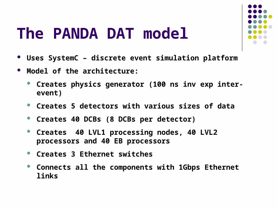
The PANDA DAT model Uses SystemC – discrete event simulation platform
Model of the architecture:
Creates physics generator (100 ns inv exp inter-event)
Creates 5 detectors with various sizes of data
Creates 40 DCBs (8 DCBs per detector)
Creates 40 LVL1 processing nodes, 40 LVL2 processors and 40 EB processors
Creates 3 Ethernet switches
Connects all the components with 1Gbps Ethernet links

The model – DCB Buffer Occupancy
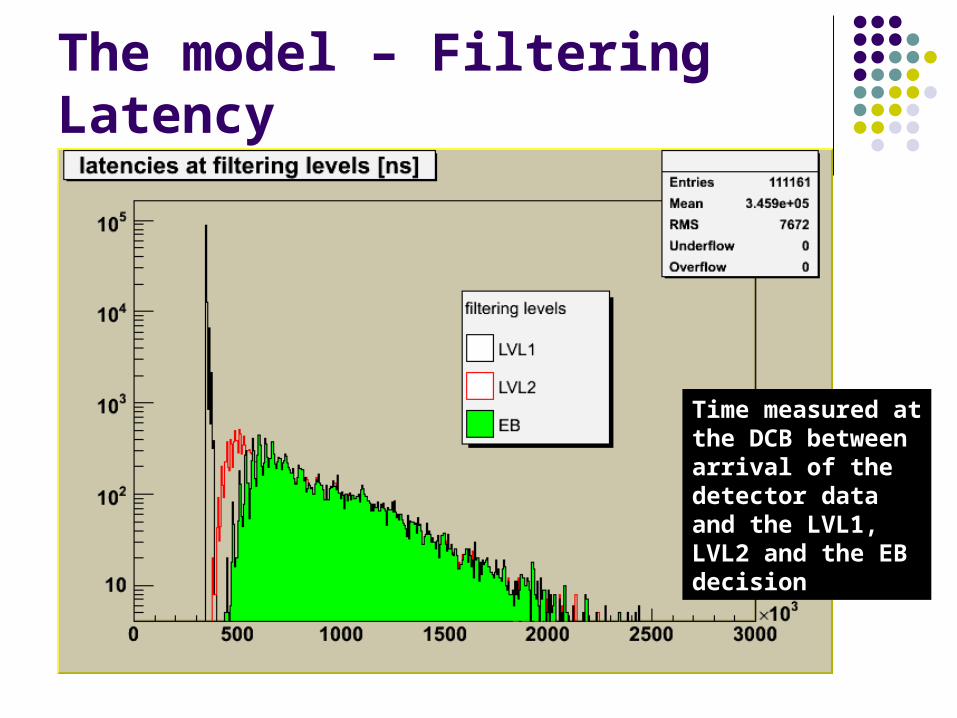
The model – Filtering Latency
Time measured at Time measured at the DCB between the DCB between arrival of the arrival of the detector data and detector data and the LVL1, LVL2 and the LVL1, LVL2 and the EB decisionthe EB decision

The model - Latency Variation
Sufficient processing resources Sufficient processing resources (number of CPUs) installed at the (number of CPUs) installed at the LVL1 processing node guarantee LVL1 processing node guarantee deterministic latency and lossless deterministic latency and lossless operation operation
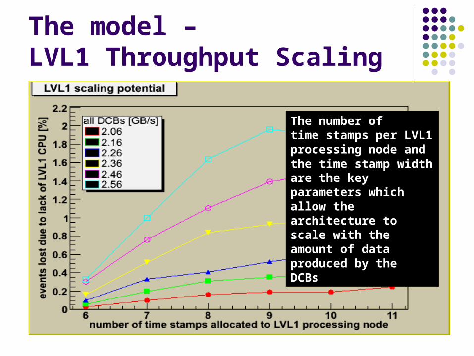
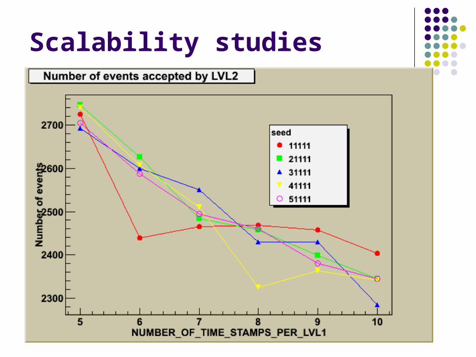
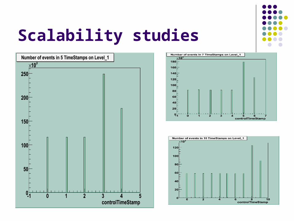
The model – LVL1 Throughput Scaling
The number ofThe number oftime stamps per LVL1 time stamps per LVL1 processing node and the processing node and the time stamp width are the time stamp width are the key parameters which key parameters which allow the architecture to allow the architecture to scale with the amount of scale with the amount of data produced by thedata produced by theDCBsDCBs
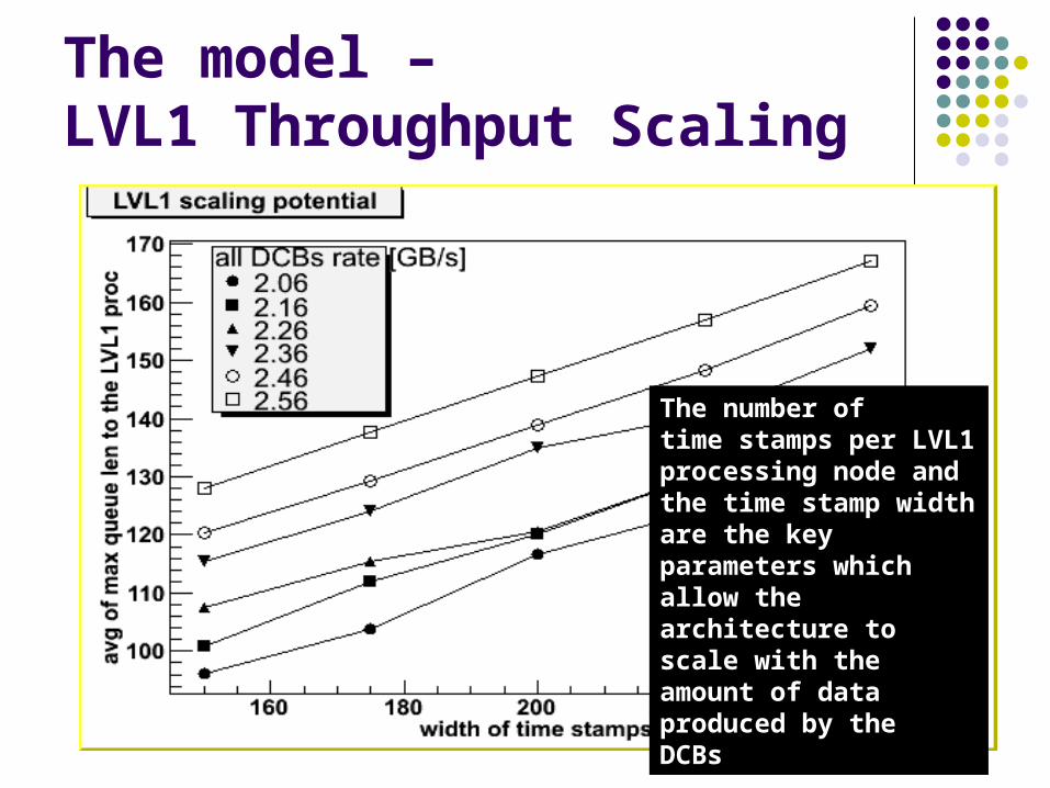

What we did so far: We proposed architecture for the continuous
sampling data acquisition system for PANDA We built behavioral model to evaluate and
understand impact of the key architectural parameters on the performance
The architecture meets requirements: operates at 10 MHz interaction rate allows for data correlation based on time stamps offers flexibility for wide range of filtering algorithms scales for increased amount of data to be transferred
and processed – this we have to prove and it is now our main focus
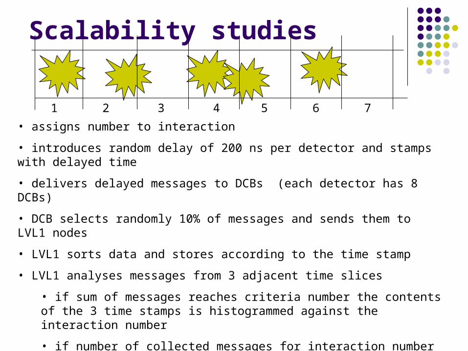
Scalability studies
1 2 3 4 5 6 7
• assigns number to interaction
• introduces random delay of 200 ns per detector and stamps with delayed time
• delivers delayed messages to DCBs (each detector has 8 DCBs)
• DCB selects randomly 10% of messages and sends them to LVL1 nodes
• LVL1 sorts data and stores according to the time stamp
• LVL1 analyses messages from 3 adjacent time slices
• if sum of messages reaches criteria number the contents of the 3 time stamps is histogrammed against the interaction number
• if number of collected messages for interaction number meets another limit the event is considered as interesting and not previously recognized – it is assigned to CPU for processing. The earliest time stamp with a message belonging to the given interaction defines INTERACTION TIME STAMP.

Scalability studies
LVL1 accepted events
0
1000
2000
3000
4000
5000
6000
7000
8000
9000
10000
0 1 2 3 4 5 6 7 8 9 10 11 12 13 14 15number of time slice
en
trie
s
7
8
9
10
11
12
7 - no delay
8 - no delay
9 - no delay
10 - no delay

Scalability studies
Scalability studies

Scalability studies

Scalability studies

Scalability studies
Scalability studies

Scalability studies

Scalability studies