modelling and simulation of the ir-drop phenomenon in
TRANSCRIPT

HAL Id: tel-00998547https://tel.archives-ouvertes.fr/tel-00998547
Submitted on 2 Jun 2014
HAL is a multi-disciplinary open accessarchive for the deposit and dissemination of sci-entific research documents, whether they are pub-lished or not. The documents may come fromteaching and research institutions in France orabroad, or from public or private research centers.
L’archive ouverte pluridisciplinaire HAL, estdestinée au dépôt et à la diffusion de documentsscientifiques de niveau recherche, publiés ou non,émanant des établissements d’enseignement et derecherche français ou étrangers, des laboratoirespublics ou privés.
Modelling and Simulation of the IR-Drop phenomenonin integrated circuitsMarina Aparicio Rodriguez
To cite this version:Marina Aparicio Rodriguez. Modelling and Simulation of the IR-Drop phenomenon in integratedcircuits. Other. Université Montpellier II - Sciences et Techniques du Languedoc, 2013. English.NNT : 2013MON20060. tel-00998547

Délivré par UNIVERSITE MONTPELLIER 2
Préparée au sein de l’école doctorale : Information, Structures, Systèmes
(I2S)
Et de l’unité de recherche : Systèmes Automatiques et Microélectroniques
(SYAM)
Spécialité : Microélectronique
Présentée par Marina Aparicio Rodriguez
Soutenue le 06/12/2013 devant le jury composé de
M. Michel RENOVELL, Directeur de Recherches,
CNRS, LIRMM, Université Montpellier II
Directeur de thèse
Mme. Mariane COMTE, Maître de Conférences,
LIRMM, Université Montpellier II
Co-encadrant de thèse
M. Laurent LATORRE, Professeur,
LIRMM, Université Montpellier II Examinateur
M. Joan FIGUERAS, Professeur,
Université Polytechnique de Catalogne Rapporteur
M. Jean-Michel PORTAL, Professeur,
Ecole Polytechnique Universitaire de Marseille Rapporteur
M. Ilia Polian, Professeur,
Université de Passau Examinateur
M. Bernd BECKER, Professeur,
Université Albert-Ludwings
Examinateur
Mme. Florence AZAIS, Chargée de Recherches
CNRS, LIRMM, Université Montpellier II
Invité
Modeling and simulation of the IR-Drop
phenomenon in integrated circuits

2

3
Abstract
Scaling technology in deep-submicron has reduced the voltage supply level and increased the number
of transistors in the chip, increasing the power supply noise sensitivity of the ICs. Excessive power supply
noise affects the timing performance, increasing the gate delay, and may cause timing faults. Specifically,
power supply noise induced by the currents that flow through the resistive parasitic elements of the Power
Distribution Network (PDN) is called IR-Drop.
This thesis deals with the modelling and simulation of logic circuits in the context of IR-drop. An
original algorithm is proposed that allows to perform an event-driven delay simulation of the logic Block
Under Test (BUT) while taking into account the whole chip IR-drop impact on the simulated block. To do
so, we develop accurate and efficient electrical models for the currents generated by the switching gates,
the propagation of the current draw through the PDN and the gate delays. First, the pre-characterization
process for the dynamic currents, static currents and gate delays is described to generate a gate library.
Then, another pre-characterization procedure is suggested to estimate the current distribution through the
resistive PDN model. Our models are implemented in a first version of the simulator developed by the
University of Passau in the context of collaboration. In addition, the impact of the parasitic capacitive
elements of the PDN is analyzed and a procedure to derive the current distribution in a resistive-capacitive
PDN model is proposed.

4

5
Résumé
L’évolution des technologies microélectroniques voire déca-nanoélectroniques conduit simultanément
à des tensions d’alimentation toujours plus faibles et à des quantités de transistors toujours plus grandes.
De ce fait, les courants d’alimentation augmentent sous une tension d’alimentation qui diminue, situation
qui exacerbe la sensibilité des circuits intégrés au bruit d’alimentation. Un bruit d’alimentation excessif se
traduit par une augmentation du retard des portes logiques pouvant finalement produire des fautes de
retard. Un bruit d’alimentation provoqué par des courants circulant dans les résistances parasites du
Réseau de Distribution d’Alimentation est communément référencé sous la dénomination d’IR-Drop.
Cette thèse s’intéresse à la modélisation et à la simulation de circuits logiques avec prise en compte du
phénomène d’IR-Drop. Un algorithme original est tout d’abord proposé en vue d’une simulation de type
‘event-driven’ du bloc logique sous test, en tenant compte de l’impact de l’ensemble du circuit intégré sur
l’IR-Drop du bloc considéré. Dans ce contexte, des modèles précis et efficaces sont développés pour les
courants générés par les portes en commutation, pour la propagation de ces courants au travers du réseau
de distribution et pour les retards des portes logiques. D’abord, une procédure de pré-caractérisation des
courants dynamiques, statiques et des retards est décrite. Ensuite, une seconde procédure est proposée
pour caractériser la propagation des courants au travers du réseau de distribution. Nos modèles ont été
implantés dans une première version du simulateur développé par nos collègues de Passau dans le cadre
d’une collaboration. Enfin, l’impact des éléments capacitifs parasites du réseau de distribution est analysé
et une procédure pour caractériser la propagation des courants est envisagée.

6

7
Acknowledgements
It would not be possible to do this work without the help and kind support of people around me. To
only some of whom it is possible to give particular mention here.
First of all, I would like to thanks my advisor, Dr. Michel Renovell, and my co-supervisor,
Dr. Mariane Comte, for their patient guidance, encouragement and advices during these three years. I
would like to express my gratitude for sharing their experience and supervising me in all steps of this
work. It was a great pleasure to work with them.
I also appreciate working with Dr. Ilian Polian and Jie Jiang from the Department of Computing
Engineering of the University of Passau. I would like to thanks them for this productive collaboration.
Finally, I would like to express my gratitude Dr. Joan Figueras, Dr. Jean-Michel Portal,
Dr. Laurent Latorre, Dr. Florence Azais and Dr. Bernd Becker, for accepting to be members of the jury
and coming to Montpellier (not without some unexpected problems).
Personally, I would like to thank my parents, Angel and Amparo, and my sister Paula. They have been
there for me every step of the way, have always loved me unconditionally, and have aided me through all
of my decisions.
Last but not the least, I would like to thank my partner, Thomas, who endured this long three years
with me, supporting me in the worst moments and making rich the SNCF with so much travels. Without
his support, patience and love, this adventure would not have been possible.

8

9
TABLE OF CONTENTS
Abstract ................................................................................................................................................... 3
Résumé.................................................................................................................................................... 5
Acknowledgements ................................................................................................................................. 7
TABLE OF CONTENTS ........................................................................................................................ 9
General introduction ............................................................................................................................. 11
1 Introduction ................................................................................................................................. 15
1.1 Context and state of the art ...................................................................................................... 15
1.1.1 Power supply noise and IR-Drop definition .................................................................... 15
1.1.2 Power supply noise analysis ............................................................................................ 16
1.1.3 The design approach ........................................................................................................ 18
1.1.4 The test approach ............................................................................................................. 20
1.2 Objective and motivation ........................................................................................................ 25
1.3 Algorithm principle ................................................................................................................. 27
1.4 Physical vs electrical structure of the grid ............................................................................... 32
2 Electrical model at gate level ...................................................................................................... 35
2.1 Dynamic and static currents .................................................................................................... 35
2.2 Library models and variable parameters ................................................................................. 40
2.3 Library pre-characterization .................................................................................................... 42
2.3.1 Delay model .................................................................................................................... 44
2.3.2 Dynamic current model ................................................................................................... 49
2.3.3 Static current model ......................................................................................................... 52
2.4 Pre-characterization constraints ............................................................................................... 56
2.5 Self IR-Drop ............................................................................................................................ 57

10
3 Electrical model of the PDN current distribution ........................................................................ 61
3.1 Electrical model for the current distribution in a resistive grid ............................................... 62
3.1.1 PDN resistive model ........................................................................................................ 62
3.1.2 The distribution factor ..................................................................................................... 64
3.2 Electrical model for the current distribution in a resistive and capacitive grid ....................... 75
3.2.1 Different types of capacitive elements ............................................................................ 76
3.2.2 Analysis of the capacitive elements ................................................................................ 77
3.2.3 Theoretical analysis and simplified model ...................................................................... 86
3.2.4 Electrical model for capacitive elements ......................................................................... 93
4 Simulator implementation ........................................................................................................... 97
4.1 Simulation principle and validation ......................................................................................... 98
4.1.1 Simulator algorithm ......................................................................................................... 98
4.1.2 Simulation validation .................................................................................................... 102
4.1.3 Validation with a circuit designed to maximize the induced delay ............................... 108
4.2 Problematic of the simulation implementation using a RC grid............................................ 112
4.2.1 Capacitance window ...................................................................................................... 113
4.2.2 Simplified model ........................................................................................................... 117
4.2.3 RC model validation and conclusion ............................................................................. 132
5 General conclusion and future work .......................................................................................... 139
Annex .................................................................................................................................................. 143
TABLE OF FIGURES ........................................................................................................................ 149
LIST OF TABLES .............................................................................................................................. 153
REFERENCES ................................................................................................................................... 155
LIST OF PUBLICATIONS RELATED TO THIS THESIS .............................................................. 161

11
General introduction
Progress in deep submicron technology is focused on the increase of the transistor density in the chip
and the increase of the circuit performances such as functional frequency. As a result, important power
density problems due to the large amount of current required from the Power Distribution Network (PDN)
have appeared, increasing the power supply noise. Excessive power supply noise can affect the circuit
performances, causing problems such as signal integrity or additional delay. One of the main sources of
power supply noise is the IR-Drop: an electrical phenomenon associated to the switching of logic gates.
The inherent parasitic resistive elements of the PDN combined with the current drawn by the switching
gates produce fluctuations in the supply voltage level. This work focuses on the supply voltage noise
produced by the IR-Drop.
Design and optimization of the chip PDN is a very complex task because it is almost impossible to
anticipate all the possible operational conditions of the chip. Nevertheless, designers try obviously to
estimate the power supply noise and reduce as much as possible the IR-drop effects at the chip level. To
do so, different supply network models have been proposed. Most of these works are based on vector-less
approaches and primarily target the spatial impact of the IR-drop. Although design approaches obviate the
vector dependence of the IR-Drop phenomenon, the statistical models allow to estimate the average power
consumption at the chip level. This information is very useful to identify the critical areas and to
consequently modify the PDN structure in order to minimize the undesirable voltage drop.
Concerning the test approach, the problematic is somehow different since the goal is to verify that the
chip does not present any functional problem related to excessive delay due to IR-Drop. In this case, not
only the spatial effect should be taken into account but also the temporal effect. Therefore power supply
voltage analysis has to be addressed through a vector-dependent approach. However a vector-dependent
approach is very time consuming and limited to the block level.

12
This document deals with the IR-Drop phenomenon from a test perspective, in particular, the
modelling and simulation of logic blocks in presence of IR-Drop. The aim is to take into account the most
relevant characteristics of the IR-Drop phenomenon in the block simulation:
· IR-Drop is a global phenomenon. The switching activity of a given block generates voltage
drop impacting the whole chip. For this reason, voltage drop generated by the neighboring
blocks must be taken into account during the block simulation.
· Voltage drop due to the IR-Drop dissipates in time and in space. Therefore, this works must
develop accurate and efficient electrical models that allow a spatial and temporal simulation.
· IR-Drop phenomenon comes from the logic switching activity. So IR-Drop requires a logic
vector-dependent simulation together with an electrical simulation to estimate the voltage
drop in the PDN. Consequently, a mixed-mode simulation is necessary.
Therefore, an original algorithm is proposed allowing to perform an event-driven logic and timing
simulation of the logic block under test while taking into account the whole chip IR-Drop impact on the
simulated block. For the electrical simulation, accurate electrical models of the current draws and the gate
delays are developed, as well as an electrical model that allows to compute the current distribution through
the PDN. Our electrical models are implemented by the University of Passau in a first version of the
simulator MIRID: Mixed-mode IR-Drop Induced Delay simulator. The development of the MIRID
simulator is a joint project of LIRMM and the University of Passau funded by the German Research
Council (DFG grant PO 1220/1-2) and by the BFHZ project FK 39-10.
This document is structured in four chapters followed by a general conclusion. In Chapter 1 an
extensive description of the state of the art is presented, including the design and test approaches. The
motivation of this work and the objective are also described in detail and then, the fundamental simulation
principles are introduced.
In Chapter 2 the pre-characterization procedure to derive the gate library from SPICE simulations is
explained. This library contains the electrical models for the parameters involved in an IR-Drop
phenomenon at the gate level: dynamic currents, static currents and gate delays. All these elements are
closely related to the technology and thus, a pre-characterization procedure is required for every
technology. Other electrical parameters are taken into account to build the gate library: the input voltage
swing, the supply voltage swing and the output capacitance. The used pre-characterization procedure to
derive the electrical model from SPICE simulations for the dynamic current, static current and gate delay

13
for any electrical configuration is presented. Limitations of this pre-characterization process are also
described.
Chapter 3 deals with the description of an electrical model for the PDN. This chapter is divided in two
main sections: a first section where the PDN is modeled as a resistive grid and a second one where the
capacitive elements present in the PDN are included in the resistive grid. For the resistive model, the
current distribution through the grid is analyzed and a set of distribution factors is characterized. This set
allows to estimate the current distribution through the resistive grid, taking into account the edge effect.
Furthermore, a procedure to consider the impact of the neighboring blocks is proposed. In the second
section, an extension of the electrical model of the PDN is presented. The impact of the capacitive
elements in the current distribution through the PDN is analyzed and an electrical model is proposed for
the three main capacitive elements present in the PDN: parasitic capacitors of the physical PDN,
intentional decoupling capacitors and intrinsic decoupling capacitors due to non-switching gates.
Chapter 4 is also structured in two main sections. In the first one the simulation algorithm
implemented in MIRID is described in detail. Then, signal waveforms and induced delays obtained from
MIRID and SPICE simulations are compared in order to validate the gate library and the distribution
factor principle. In the second section, we analyze the problem of implementing a PDN model with
capacitive elements in the simulator. Mathematical computation of the current distribution is not possible
due to the complexity and thus, a simplification method is described in order to estimate the current
distribution. Although this method is not fully implemented in the simulator, preliminary simulations
applying it are presented.

14
15
1 Introduction
1.1 Context and state of the art
1.1.1 Power supply noise and IR-Drop definition
Progress in deep submicron design is focused on the reduction of power consumption and the increase
of the number of transistors in the devices. Simultaneously, technology scaling has continued to improve
the performance of processors increasing the functional frequency. On the one hand, voltage scaling has
reduced significantly the noise margin and, on the other hand, the ultra-high transistor density and rising
frequency lead to a power density problem: a large amount of current is required, increasing the power
supply noise [1]. As a result, excessive power supply noise can significantly affect the circuit
performances and cause problems such as signal integrity [2] or additional delay [3]. Therefore, the
increase of power supply noise has become a critical element in the performance and reliability of
manufactured chips.
Power Supply Noise (PSN) refers to the voltage fluctuations in the power and ground distribution
networks (PDN). The voltage fluctuations due to power supply noise in the PDN are generally called
voltage drop. The power distribution network includes all the metal wires and vias that deliver power to
every gate in the chip. This on-chip PDN is predominantly resistive but capacitive and inductive parasitic
elements are also presented. Power supply noise is induced by current flows through the PDN:
· IR-Drop is generated due to the resistive elements of the PDN,
· ground bounce is generated due to the inductive elements of the PDN ( ).
This work focuses on power supply noise produced by IR-Drop.

16
IR-Drop is defined as an electrical phenomenon associated with the switching of MOS transistors. A
current draw appears in the power supply connection and/or the ground supply connection when
transistors switch. The inherent parasitic elements of the PDN combined with this current draw produce
fluctuations in the voltage level. IC scaling technology has increased the density of transistors and the
functional frequency. Thus, there are more gates switching simultaneously and consequently, voltage
fluctuations have also increased due to the increase of the amount of current flowing through the PDN. As
a consequence of these fluctuations, logic gates can be powered with a lower-than-normal Vdd or higher-
than-normal Gnd or both, reducing the gate swing and impacting logic gates by an increased delay.
Moreover the sensitivity of the gate delay to power supply noise increases with technology scaling. It has
been reported that fluctuations of 10% in power/ground supply voltage increase gate delay by 8% in
180nm technology [4], but fluctuations of 10% can cause up to a 30% increase in gate delay in a 130nm
technology [5], and a 1% change in power supply voltage causes nearly 4% of additional gate delay in
90nm technology [6]. The impact of power supply noise due to IR-Drop phenomenon has therefore
become a critical concern, both for design and test aspects.
1.1.2 Power supply noise analysis
As the power supply noise becomes critical, analyzing its impact on the integrated circuit electrical
behavior is today an important research topic. A good knowledge about the noise impact on the circuit
functionality and timing performance can improve the design of the PDN and the test process.
A voltage drop generated by a switching gate dissipates in time and space [7] as illustrated in Figure
1.1. Indeed, a current draw appears when the gate input switches and finishes after the commutation, when
the output has become stable. It means that the voltage drop vanishes rapidly after the switching of the
gate. On the other hand, current draw propagation is closely related to the PDN structure. The original
current draw spreads through the PDN structure. Voltage drop due to the IR-Drop in a uniform power
mesh spreads like a “bull’s eye” with “circular” equipotential rings [8]. Therefore, neighboring gates are
more concerned by the voltage drop due to the IR-Drop phenomenon than gates locate far away from the
original current draws. In brief, spatial and temporal analyses are necessary to describe the IR-Drop
phenomenon.

17
Figure 1.1: A current draw injected into a power grid dissipates quickly in time (a) and space (b) [7].
Voltage variations in the power and ground supply networks have adverse impact on the delay of the
gates connected to the supply networks and thus, timing faults can appear due to these variations.
Consequently, analyzing the induced delay due to the power supply noise is becoming an important topic.
The delay of a logic gate depends on many electrical factors such as supply voltage level, input voltage
level, load capacitor, input slew rate and other electrical parameters of the gate [9]. Todri analyses the
impact of power and ground supply noise in a path delay [10]. The conclusion is that power supply noise
reduces the drive strength by changing the operational regions of the transistor, impacts the noise
conditions on the neighboring gates by causing a speed-up or slow-down, and causes a delay shift due to
the different voltage levels among the gates. Delay variations are further aggravated with package
inductance, power/ground network parasitics, switching frequencies and technology scaling.
Regarding the electrical elements that have a significant impact on the power supply noise, we
identify three important elements: the power distribution network, the current draw of the switching gate
and the gate delay. The power distribution network and the package can be modeled as a combination of
electrical elements. In [11] Panda proposes to use the following models for the package/on-chip power
supply network:
· a RLC model for the package leads, ball grid arrays and power planes;
· a RC model for the gate to power connections;
· a RC model for intrinsic decoupling capacitance of non-switching gates;
· a RC model for intentional decoupling capacitances.

18
Regarding the electrical model at the gate level, most of the papers adopt a cell-based circuit model
for the current draw and the delay in order to estimate the power supply noise. For some of these papers,
an event-driven simulator uses the cell-library to inject a current draw into the PDN at the block level [12],
[13], [14]. Other works estimate the global power supply noise based on a statistical approximation of the
switching activity [15]. Finally other ones use the cell-library to consider the power noise information in a
fault generator model [6].
For the gate delay, an analytical approach is used representing gate delay as a linear/quadratic function
of the supply voltage in [9], [16]. Other publications propose a statistical approach to characterize delays
[3]. Standard cell delay is treated as a perturbed random variable, and the probability functions are derived
by simulating a set of characterization patterns.
For the current draw, most of the publications propose to model this current as a triangular function
[3], [17] or as a trapezoidal function [2], [18]. These models adapt the shape of the current in function of
the output capacitance and other electrical parameters. Some approximations are applied to simplify the
electrical model. For example, the peak current is assumed to coincide with the transition at the gate input
[17]. The value of the peak and the duration of the current are dependent on the gate type and the load
capacitance.
Knowing the effect of the voltage supply noise, there are two traditional research directions:
· The first direction is to predict the power supply noise during the design phase and to manage
it by design modifications.
· The second direction is to create test procedures to detect the timing faults generated by the
power supply noise.
1.1.3 The design approach
The design of a good, reliable on-chip PDN of a digital IC is a very complex task because designers
cannot anticipate all the functional conditions Design researches about the power supply sensibility try
obviously to reduce as much as possible the whole power supply noise effect at the chip level. In essence,
the principle is to estimate the supply voltage drop due to the IR-Drop and try to adapt the PDN design to
minimize this phenomenon. To this aim, some techniques are applied during design to decrease the power
supply noise and to improve the noise immunity of the circuits as explained by Larsson in [19].
The most widely used technique consists in adding decoupling capacitors between the power and
ground supplies. Decoupling capacitors prevent the power noise from spreading through the PDN and

19
their inclusion in the design allows to isolate different areas on the chip. In this context most of the works
try to develop algorithms to determine the optimal size and placement of the decoupling capacitors from
the switching activities and the spatial correlations between different blocks. A power supply noise aware
post-floorplanning methodology is proposed in [20], [21], [22]. Another research suggests to improve the
traditional decoupling capacitor and to include active decoupling capacitors as a most effective technique
to reduce the power supply noise [23].
Another classical way to reduce the power supply noise is to design a robust power distribution
network. A lot of research works mark that traditional constraints in the PDN design are not enough to
remove the IR-Drop timing faults. In order to improve the PDN design, most of the works propose a
mathematical model to address the most important issues in the PDN design: width and pitch of PDN
wires [8], [24], size, number and location of pads [25], [26], [27], [28], [29]. Wire sizing for power and
ground networks considering the IR-Drop induced by both the clocking and computing components is
suggested in [24] and considering the IR-Drop and the area constrained in [8]. In order to determine the
size, number and location of pads, [26] and [27] propose a closed form model for the power distribution
network in N-metal layer system for wire-bond and flip-chip packages in function of given design
constraints (as power dissipation, power supply voltage or static IR-Drop).
Other works focus on the correlation between different parameters of the on-chip power distribution
grid and their impact on noise [25], [28], [29]. Results from this analysis can be used as guidelines when
designing a robust power distribution network.
Models proposed by Rius [30] and by Shakeri [28], [29] exclusively focus on the IR-Drop
phenomenon. Shakeri [29] demonstrates that the PDN can be approximated as a continuous layer of
conductive material and that IR-Drop can be calculated by solving a system of partial differential
equations, i.e. Poisson equation, with the proper boundary conditions. Shakeri [29] proposes a compact
physical IR-Drop model of the on-chip power distribution grid and an IR-Drop model is derived for the
wire-bond and the flip-chip packages. In this paper, the tradeoff between the package and the on-chip
power distribution network parameters is studied in details. The size and number of pad tradeoff is also
analyzed. The optimal placement of these pads is derived to minimize the IR-Drop. In brief, Shakeri
suggests the use of a large number of small pads for the power distribution network instead of a small
number of large pads to reduce the IR-Drop.
Based on the conclusion of Shakeri, Rius [30] suggests another IR-Drop model to determine the
average power consumption of a block. Initially, the IR-Drop is modeled in an infinite PDN. Then, the IR-
Drop model in a finite PDN is derived from the infinite model solution. The suggested model provides an
20
accuracy estimation of the average power consumption of a block for the wire-bond package. Models of
Shakeri and Rius help designers in the early stage of the design to estimate accurately the on-chip and
package resources that need to be dedicated to power distribution, reducing the cost of over-design.
In brief, most of these works are based on a vector-less approach and primarily target the spatial effect
of supply voltage noise. Suggested statistical circuit models estimate the average current consumption at
the chip level, allow to identify the critical areas and to adapt the PDN network design in order to avoid
the undesirable voltage drop. Although the design approaches do not take into account the input vector
dependence of the IR-Drop phenomenon, the statistical models provide an estimated supply voltage drop
at the chip level. We remember that a vector-based simulation at the chip level is non-viable due to
prohibitive simulation costs.
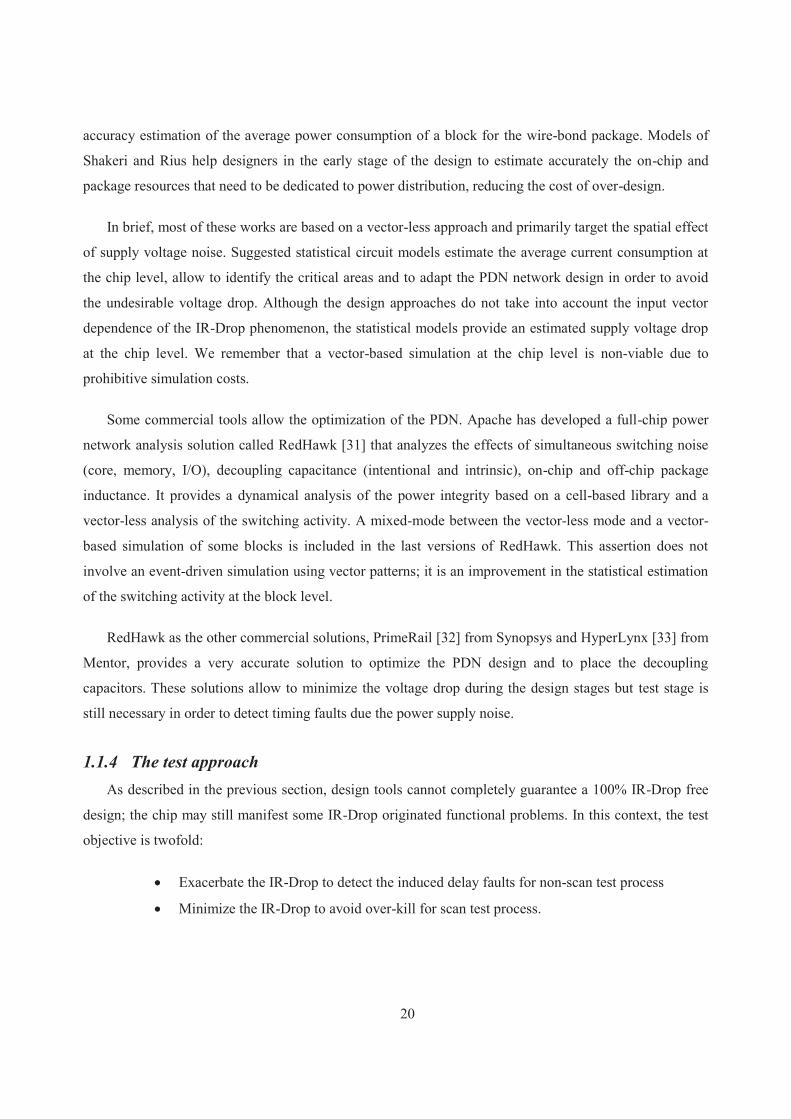
Some commercial tools allow the optimization of the PDN. Apache has developed a full-chip power
network analysis solution called RedHawk [31] that analyzes the effects of simultaneous switching noise
(core, memory, I/O), decoupling capacitance (intentional and intrinsic), on-chip and off-chip package
inductance. It provides a dynamical analysis of the power integrity based on a cell-based library and a
vector-less analysis of the switching activity. A mixed-mode between the vector-less mode and a vector-
based simulation of some blocks is included in the last versions of RedHawk. This assertion does not
involve an event-driven simulation using vector patterns; it is an improvement in the statistical estimation
of the switching activity at the block level.
RedHawk as the other commercial solutions, PrimeRail [32] from Synopsys and HyperLynx [33] from
Mentor, provides a very accurate solution to optimize the PDN design and to place the decoupling
capacitors. These solutions allow to minimize the voltage drop during the design stages but test stage is
still necessary in order to detect timing faults due the power supply noise.
1.1.4 The test approach
As described in the previous section, design tools cannot completely guarantee a 100% IR-Drop free
design; the chip may still manifest some IR-Drop originated functional problems. In this context, the test
objective is twofold:
· Exacerbate the IR-Drop to detect the induced delay faults for non-scan test process
· Minimize the IR-Drop to avoid over-kill for scan test process.

21
1.1.4.1 Maximum instantaneous current estimation
Early works propose to estimate the maximum instantaneous current in order to detect excessive
switching activity in the IC and thus, reject these devices with a high risk of timing faults. Kriplani [17]
estimates the maximum instantaneous current using a triangular function as the current draw model. In
order to determine the maximum current, a vector-less algorithm called iMax is proposed. This algorithm
computes all the possible commutations for every gate of the circuit and also all the possible associated
waveforms. But it evaluates combinations of gate excitations that may not be possible. The maximum
instantaneous current computed therefore is an upper bound of the worst case in a circuit. In addition, the
suggested iMax algorithm is limited, it only estimates the maximum current for small blocks.
Jiang and Cheng [34] propose an improvement in the maximum instantaneous current estimation.
Computation of the maximum instantaneous current is treated as an Integer Linear Programing (ILP)
problem. ILP formulation allows to compute exactly the maximum instantaneous current for a small
circuit using the gate library from [17]. For larger circuits, a partitioning-based approach is suggested.
Large circuits are divided in sub-circuits whose maximum currents are computed independently. The
maximum current of the circuit is the addition of all the maximum currents. In this case, the maximum
current computed is again an upper bound of the real maximum current. The suggested ILP computation
requires a longer CPU time in comparison with the iMax algorithm but the maximum instantaneous
current estimated for small circuits is not overestimated.
In brief, the maximum instantaneous current estimated is the worst case for a circuit and it is
overestimated. The maximum instantaneous current in a realistic operation mode would be much smaller
and thus, test based on these methods can reject fault-free chips. In addition, a high current density does
not necessary mean a delay fault, but just a risk.
1.1.4.2 Test pattern generation
In order to detect timing faults due to power supply noise some of the works propose to generate a
small set of patterns to maximize the voltage drop noise. In this case, the test objective is to target the IR-
Drop originated delay fault and to generate a delay test sequence able to exacerbate the IR-Drop
phenomenon.
Zhao [15] proposes to use Monte Carlo simulation and Genetic Algorithm in order to generate a set of
patterns that induces the maximum switching noise. In this case, an event-driven simulation based on the
correlation between switching events and a cell library is implemented. The cell library includes the delay
and switching current in function of the input and output signal slopes and the output capacitance. The

22
switching noise is modeled as a weighted sum of the switching currents and the rates of change of these
switching currents. The weights are respectively the effective resistance and inductance on the power and
ground networks experienced by each switching current. The electrical model used to determine the
effective resistance and inductance include a RL model for the packing and a RL model for the on-chip
power distribution network. Finally, Monte Carlo simulation and Genetic Algorithm are used to search for
the worst case input vector pair that induces the maximum switching noise.
Jiang and Cheng [13] also propose to generate small sets of patterns to maximize the voltage drop
noise. In this case, the cell library is characterized in function of the power and ground pin characteristics
and the power net RLC parameters as well as the starting voltage, ending voltage, and the slope of the
input voltage. For the sake of simplicity, switching currents are modeled as a triangular function that
depends on the input voltage variables. An event-driven logic simulation is developed in order to simulate
a given input pattern. The power lines of the power distribution network are model as a RC tree. First, the
effective waveforms in the power and ground lines for each small block (consisting of a set of adjacent
cells) is computed. In order to propagate the waveform through the RC tree, look-up tables are generated
in function of the electrical parameters of the power distribution network and the waveform of every cell.
Later, the circuit is simulated for an input pattern applying the derived waveform. Based on this event-
driven simulation for any given 2-vector sequence, a Genetic Algorithm is applied in order to generate a
small set of patterns that would cause high power supply noise at a specified area.
Krstic [12], [14] improves the test pattern generation of Jiang and Cheng in order to sensitize the
selected paths. The fitness value of the pattern is calculated as a summation of the maximum power supply
noise for the nodes on the selected path. The Genetic Algorithm generates a set of pattern that maximizes
the voltage supply noise in the nodes along the selected paths.
In summary, Zhao [15], Jiang and Cheng [13] developed event-driven simulators that allow to
estimate the maximum power supply noise. However, both simulators compute the global power supply
noise and do not take into account the impact of the power supply noise on the gate delays and on the
switching currents. Although Jiang and Cheng [13] derive the waveform current in a RC tree, the
estimation of the supply voltage noise through the on-chip power distribution network is not computed.
Moreover, test pattern generated using these methods maximize the voltage supply noise and thus, present
the same problem as the method based on the computation of the maximum instantaneous current.

23
Some other works tackle the pattern generation focusing on the type of voltage drop. Bhowmick [35]
classifies the voltage drops into three broad categories following their locality in time and space:
· Low Frequency Power Drop (LFPD) affects the entire PDN after a few clock cycles
· High Frequency Power Drop (HFPD) in highly localized and is effective in the same clock
cycle
· Mid Frequency Power Drop (MFPD) is localized in a small area but effective for more than
a single clock cycle.
Polian [36] proposed a heuristic method to generate test sequences that create worst-case power drop
by accumulating high and low frequency. To do so, Polian employs a dynamically constrained version of
the classical D-algorithm to generate a sequence that maximizes the effects of both LFPD and HFPD.
Bhowmick [35] addresses the problem of the multi-cycle droop faults due to the MFPD. A SAT-solver
based ATPG for detection of these faults is developed for both combinational and full-scan circuits.
Similarly to Polian, the resulting switching activity from the generated test vector may generate much
higher power density and much higher IR-drop than in functional mode. In addition, both methods target
the generation of switching activity without taking into account the electrical parameters at the gate level.
Another classical direction for IR-Drop testing is to try to adapt the test patterns to the realistic
behavior of the tested circuits. It is known that power consumption during at-speed delay test can be
different than during functional operation. Often a large number of transitions occur within a short time
frame during the test operation in comparison with the normal circuit operation. In addition, test patterns
can generate high switching activity in a small area of the circuit, increasing significantly the IR-Drop. It
means that the test patterns applied in the test procedure generate an unrealistic IR-Drop and fault-free
chip can be discarded. The objective of these works [37-44] is to adapt the test pattern generation for the
at-speed delay test considering the IR-Drop.
Saxena [37] proposes to reduce the switching activity of the test patterns. This paper analyses the IR-
Drop during at-speed test. Concretely, the toggling events are counted while a scan-based transition test is
performed. Analyzing the toggle activity during a clock cycle, the study concludes that the toggle activity
of certain pattern obtained from the ATPG is exacerbated in the first frames of the clock cycle. Saxena
concludes that generation of patterns implying a more constant switching activity during a clock cycle
reduces the peak of power consumption.

24
A method to generate patterns is proposed by Tehranipoor in a series of works [38], [39]. A statistical
IR-drop analysis is performed to determine the blocks that consume more power and consequently endure
a higher IR-Drop during the test pattern application. The probability of net toggle activity over the entire
cycle period is derived from the statistical analysis. As most of the switching activity occurs during the
early clock cycle period [37], the Switching Time Frame (STW) is identified as a more efficient unity of
time than the clock cycle period. As the STW is variable in function of the test vector, the average
switching time frame window is computed for every block. Consequently, the average switching power
threshold for every block is estimated. On the other hand, a dynamic IR-Drop analysis is implemented and
the average power consumption during the switching time frame (referred as switching cycle average
power or SCAP) is calculated for every ATPG test pattern, rather than during a single tester cycle. Finally,
test patterns with an associated SCAP over the average switching power threshold are discarded due to
their exacerbated switching activity.
Other works address the distribution of switching on the chips. Certain test patterns generate hot-spots
and consequently, high levels of IR-Drop appear in small areas of the chip. Lee [40] proposes a method to
select test patterns from ATPG whose switching activity is distributed through the whole chip. The test
pattern transitions are monitored: when a gate switches, the gate information and the load from the fan-
outs are stored into the pattern transition profile set. In function of this information, Lee proposes to derive
a Weighted Switching Activity matrix WSA from the complete profile sets for every test pattern. The
WSA matrix represents the switching weights of a hypothetical single pattern during the launch-on-
capture cycle. In addition, Lee derives the Maximum Weighted Switching Activity WSAmax. The WSAmax
matrix represents the maximum switching weights for a circuit independently of the test patterns. In order
to reduce the number of test patterns, the test patterns are compacted such that the resulting WSA
associated to the compacted test patterns do not exceed the switching threshold that is defined as a
percentage of the highest maximum WSAmax. The paper concludes that fixing the switching threshold
around 20%, 25% and 30% of the maximum switching, the test coverage does not decrease significantly.
Other works use the ‘X-filling’ approach to reduce IR-drop effect during at-speed test. The X-filling
method assigns 0's and 1's to unspecified ‘X’ bits in a test cube obtained from ATPG. This method
reduces the circuit switching activity in capture mode and it is claimed that the X-filling method can be
easily incorporated in the test flow because it requires only minimal changes in the existing ATPGs. In
addition, the method does not affect the test data volume and the test time. Wen et al. propose a X-filling
technique to reduce the IR-drop effect in a series of work [41], [42], [43]. In [41], only flip-flops transition
activity is considered while in [42], both flip-flop and gate transition activities are studied. In [43], the
authors focus on preventing the IR-Drop especially on gates that are close to the activated critical paths.

25
Other authors propose improvements in the X-filling method to reduce the IR-Drop during at-speed test: J.
Li in [44] proposes to reduce both shift power and capture power during at-speed testing by improving the
X-filling technique: i-filling method. In [45], spatial information is taken into account to reduce the IR-
Drop effect during at-speed scan test. The IR-drop effect for each region is estimated using the WSA cost
function.
In brief, the objective of these works is to minimize the IR-drop phenomenon while generating a test
sequence during scan-test. In these works the used PDN model is very simplified and it is not
representative of the whole chip IR-Drop impact.
1.1.4.3 Voltage drop fault models
Tirumurti [6] proposes a Generalized Fault Model (GFM) where power noise information is
considered. A static timing analysis is performed instead of an expensive dynamic analysis. The waveform
characterization is developed for every cell in function of the fanout and input signal slope. According to
the layout, the suggested method classifies the cells as aggressor cells or victim cells. Obviously, power
lines with a high number of aggressor cells will be more affected and so more sensitive to voltage drop.
Areas affected by an important IR-Drop are detected using this procedure. Unfortunately, the worst
voltage droop estimated by the fault simulator would never appear in functional mode because not all the
aggressor cells will necessarily switch simultaneously during functional operation.
1.2 Objective and motivation
Regardless of maximizing or minimizing its impact, the IR-Drop phenomenon has become a critical
point during the test phase and thus, IR-Drop induced delay has to be considered, predicted and evaluated
in this phase. Direct dependence between switching activity, power noise and delay faults requires an
accurate vector-dependent simulation. Therefore, the objective of this work is to develop a vector-
dependent IR-Drop timing-aware and logic simulation in order to be able to simulate test pattern
sequences and to detect the appearance of delay faults. The challenge here comes from two strong
limitations:
· Chip level. Classical fault oriented simulators (stuck-at faults, bridging faults…) are focused
on the fault site and its propagation. In the case of IR-drop, there is no fault site, it is a global
phenomenon generated by the chip as a whole. So to evaluate the IR-Drop impact, a global
electrical model should be used together with an accurate vector-dependent simulation at the
chip level. Obviously, it is not feasible. In the context of the PDN design optimization,
developed models cannot be used for vector-dependent simulation due to prohibitive

26
simulation costs. In the test context, most of the works published in the literature use very
simplified models of the PDN that permit to perform vector-dependent simulation. Of course,
this is not representative of the whole chip IR-drop impact. Our objective is to propose a more
refined model of the PDN that permits to take into account the whole chip IR-drop impact
with a reasonable simulation cost.
· Block level. By definition IR-drop is an electrical phenomenon that implies currents flowing
through resistances of the PDN. Consequently, IR-Drop generates supply voltage fluctuations
that the electrical simulation at PDN level must evaluate. Electrical simulation using
traditional electrical tools (SPICE-like simulation) is not feasible due to the prohibitive
simulation cost and memory-constrained computation. The aim here is to develop an accurate
and efficient model for the currents generated by the switching gates, the propagation of the
currents through the PDN and the gate delays as a function of the voltage drop.
According to the above described simulation constraints, the simulation principles must be adapted
taking into account the complexity of the electrical simulation of the PDN and the complexity of the logic
simulation of the logic block. Therefore, the proposed electrical model must be a tradeoff between
accuracy and a reasonable simulation time.
In this work, we propose a mixed-mode simulation including a logic and electrical simulation that
allows to validate an input sequence of vectors at the block level. The voltage drop prediction will be a
combination of the mixed logic-electrical simulation at the block level and the impact of the average
consumption of the neighboring blocks. This means that the global impact of the IR-Drop is taken into
account to increase the precision in the delay estimation.
However, electrical simulation at the block level is much time consuming and almost unfeasible.
Consequently, the simulation principles must be optimized. One of the aims is therefore to propose an
accurate electrical model that allows to perform a simplified electrical simulation without loss of accuracy
in the gate delay prediction. The electrical model includes two main aspects, the gate level and the PDN
level.
· Gate level. SPICE-like simulation of transistors is too complex and useless in our context.
For our induced delay simulator not all electrical elements are concerned in the IR-Drop
phenomenon and thus, these ones should be omitted. Roughly speaking, at the gate level there

27
are two parameters of interest: the gate current draw that flows through the PDN and the gate
delay.
· PDN level: Supply voltage fluctuations may be predicted from the electrical elements of the
PDN and the current flowing through these elements. Consequently, an accurate electrical
model of the PDN including the most relevant elements, such as resistance, capacitance and
inductance, must be proposed and more importantly, an efficient model to determine the
current distribution inside the elements of the PDN needs to be defined.
Knowing that currents flowing through the PDN are a determinant point in the supply voltage
prediction and thus also in the induced delay prediction, these currents can be classified in two general
groups according to their time characteristics: dynamic and static currents. Dynamic currents correspond
to the current draws generated when gates are switching. They flow from the PDN through the gate to the
output capacitance or symmetrically, from the output capacitance to the PDN. Static currents are currents
that flow across a logic gate while the gate inputs are stable and non-switching. It means that gates are
consuming power permanently, but these currents are much smaller than dynamic currents. Both currents
are extensively described in Chapter 2. Note that neighboring blocks also generate current activity. As
justified previously, supply voltage noise is a global phenomenon at the chip level and so, the simulator
must take into account the average current generated by the neighboring blocks (section 3.1.2.3).
Although average current is a stochastic estimation, this estimation allows us to include the neighboring
switching activity in our model without increasing the simulation cost.
1.3 Algorithm principle
An event-driven simulation algorithm is suggested to estimate the induced delays generated by the IR-
Drop. As commented in the previous section, the IR-Drop algorithm principle is strongly dependent on a
local-global duality on the one hand and on an electrical-logical duality on the other hand. The aim is to
perform a logic vector-dependent block simulation at the block level that determines the logic and
switching activity of the block and an electrical simulation of the PDN that estimates the supply voltage
fluctuation.
Therefore, the general structure of the simulator is highly determined by this electrical-logical duality.
The simulator is structured into two parts that correspond to the electrical level and the logical level:
· Electrical PDN model. The PDN model is a combination of resistors, capacitors and
inductances representing the parasitic elements of the real PDN. In fact, the PDN is made of

28
two independent but completely similar PDNs: one for Vdd called Vdd PDN and one for Gnd
called Gnd PDN. Complexity of the PDN model determines the precision in the supply
voltage estimation and thus the accuracy of the delay estimation. For example, the model can
be very simple as in the traditional delay induced simulators where PDN are not concerned in
the delay estimation. For the first version of our simulator, the PDN is modeled as a resistive
two dimensional grid (section 3.1). A more complex PDN model including capacitive
elements is considered in Chapter 3 for a future version of the simulator.
· Logical block model. The logical model includes all logic gates of the block and their logic
connections. The model also includes the connection of each gate to the Vdd PDN and Gnd
PDN.
Therefore, the logic gates of the block being connected to the electrical PDN, every gate is assigned a
node of the Vdd PDN and a node of the Gnd PDN. Figure 1.2 illustrates the general structure of the
simulator and the connection between both models.
Electrical
structure of the
Vdd PDN model
Electrical
structure of the
Gnd PDN model
Logical structure
of the logic
block model
Interconnected
electrical
components : R, C, L…
Interconnected logic gates
< #logic gate, #electrical node>
Ni
Ni Interconnected
electrical
components : R, C, L…
< #logic gate, #electrical node>
Figure 1.2: General structure of the simulator
29
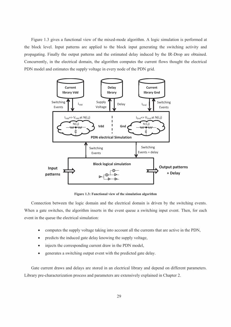
Figure 1.3 gives a functional view of the mixed-mode algorithm. A logic simulation is performed at
the block level. Input patterns are applied to the block input generating the switching activity and
propagating. Finally the output patterns and the estimated delay induced by the IR-Drop are obtained.
Concurrently, in the electrical domain, the algorithm computes the current flows thought the electrical
PDN model and estimates the supply voltage in every node of the PDN grid.
Input
patterns
PDN electrical Simulation
Block logical simulation
Switching
Events
Output patterns
+ Delay
Current
library Vdd
Delay
library
Vdd
Delay
N(i,j) N (i,j)
Current
library Gnd
Switching
Events + delay
Gnd
Switching
Events IVdd Switching
Events
IVdd=> VVdd at N(i,j) IGnd=> VGnd at N(i,j)
Supply
Voltage IGnd
Figure 1.3: Functional view of the simulation algorithm
Connection between the logic domain and the electrical domain is driven by the switching events.
When a gate switches, the algorithm inserts in the event queue a switching input event. Then, for each
event in the queue the electrical simulation:
· computes the supply voltage taking into account all the currents that are active in the PDN,
· predicts the induced gate delay knowing the supply voltage,
· injects the corresponding current draw in the PDN model,
· generates a switching output event with the predicted gate delay.
Gate current draws and delays are stored in an electrical library and depend on different parameters.
Library pre-characterization process and parameters are extensively explained in Chapter 2.

30
Cload
Vdd PDN model
Logic block
d
Gi
Ngndi
Nvddi
t0
INgndi
Gnd PDN model
t
t0
INvddi t
Nvddi-1
Ngndi-1
t0 t0+d
Gi-1
Figure 1.4: Didactic view of the mixed-mode simulation
Figure 1.4 gives a didactic view of the simulation principle. Given a gate Gi connected to the PDN at
node Nvddi for the power supply and node Ngndi for the ground, when the gate input switches at time t0,
the simulation performs the following steps:
· Computation of the power supply voltage (t0) using the electrical model of the Vdd
PDN.
· Computation of the power supply voltage (t0) using the electrical model of the Gnd
PDN.
· Computation of the voltage swing Vswing1 of the input signal:

31
1.1
· Computation of the power supply voltage (t0) using the electrical model of the Vdd
PDN.
· Computation of the power supply voltage (t0) using the electrical model of the Gnd
PDN.
· Computation of the voltage swing Vswing2 of the switching gate:
1.2
· Library access to get the corresponding delay d of the gate Gi as a function of Vswing1, Vswing2
and the load capacitance Cload:
1.3
· Library access to get the corresponding current (t0) in the power supply node Nvddi and
the current (t0) in the ground supply node Ngndi as a function of Vswing1, Vswing2 and the
load capacitance Cload:
1.4
1.5
· Computation of the and currents propagation into the Vdd PDN and Gnd PDN
using the PDN electrical models.
· Logic computation of the gate output signal at time t0 + δ

32
1.4 Physical vs electrical structure of the grid
So far, the PDN has been presented as one of the most important elements to model accurately
because currents flowing through the PDN and the resulting supply voltage fluctuations determine the gate
delays and the potential delay faults. As it is well known, PDN is a complex system of wires delivering
power to the whole integrated circuit through different layers. A PDN is classically organized as a set of
parallel large wires located in the upper metal layers covering the whole circuit surface [30]. Obviously,
the electrical PDN model depends on the physical structure of the PDN. For the sake of simplicity, we
assume the following classical structure:
· In the top metal levels of the chip, high metal level #n and metal level #n-1 are exclusively
composed of a set of parallel metal lines, these two sets having orthogonal directions. In the
high metal levels through-vias that connect the two sets of orthogonal lines are regularly
placed. The whole set of metal lines and through-vias creates a regular two-dimensional
distribution network as represented in Figure 1.5.a. Usually, in a given level, one line over
two is dedicated to Vdd and every other line to Gnd [36]; in this way, it is possible to analyze
the Vdd distribution network and the Gnd distribution network as two independent three-
dimensional distribution networks. Figure 1.5.a illustrates the two orthogonal networks for
Vdd PDN and Gnd PDN.
· In the bottom metal levels of the chip, metal #2 is commonly used for the Vdd and Gnd lines.
The Vdd and Gnd lines in the metal #2 level have typically a small length corresponding to
the mega-cell they feed [36]. In addition they have multiple parallel via connections to the
upper regular three-dimensional network as illustrated in Figure 1.5.c.
· Finally, intermediate metal level represents the interface between the upper regular three-
dimensional network and the lower irregular structure as illustrated in Figure 1.5.b.
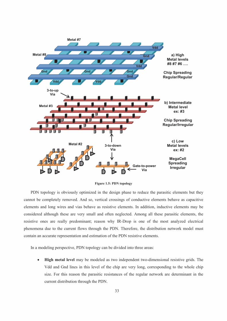
33
a) High Metal levels
#8 #7 #6 ….
Chip Spreading
Regular/Regular
b) Intermediate
Metal level ex: #3
Chip Spreading
Regular/Irregular
c) Low
Metal levels
ex: #2
MegaCell Spreading
Irregular
3-to-down
Via
3-to-up
Via
Gate-to-power
Via
Metal #8
Metal #7
Metal #3
Metal #2
Gnd
Gnd
Gnd
Vdd
Vdd
Vdd Vdd
Gnd Gnd
Figure 1.5: PDN topology
PDN topology is obviously optimized in the design phase to reduce the parasitic elements but they
cannot be completely removed. And so, vertical crossings of conductive elements behave as capacitive
elements and long wires and vias behave as resistive elements. In addition, inductive elements may be
considered although these are very small and often neglected. Among all these parasitic elements, the
resistive ones are really predominant; reason why IR-Drop is one of the most analyzed electrical
phenomena due to the current flows through the PDN. Therefore, the distribution network model must
contain an accurate representation and estimation of the PDN resistive elements.
In a modeling perspective, PDN topology can be divided into three areas:
· High metal level may be modeled as two independent two-dimensional resistive grids. The
Vdd and Gnd lines in this level of the chip are very long, corresponding to the whole chip
size. For this reason the parasitic resistances of the regular network are determinant in the
current distribution through the PDN.

34
· Intermediate metal level may be considered as included in the two-dimensional grids.
· Low metal level is made of short metal connection (in the order of the mega-cell dimension)
in comparison with the high metal level wires (in the order of the chip dimension). Moreover,
there are multiple parallel via connections to the metal #3 lines that enable to reduce the
resistive behavior of metal #2 lines. For these reasons, the parasitic resistance of this level can
be neglected in the model.
In conclusion, the electrical model of the PDN concerns the two independent supply networks, which
are physically regular, intertwined and orthogonal from one level to the other, and correspond to the high
metal levels. We can accurately model the PDN as a symmetrical structure composed of two grids with
resistive elements.

35
2 Electrical model at gate level
As introduced in the previous chapter, due to some current flows through the PDN, a supply voltage
drop appears affecting the expected delays of the switching gates and so may generate timing faults. The
current flows through the PDN can be created by logic gates that switch. Indeed, when a gate switches, a
current is drawn from the voltage source to the gate through the PDN. This current generates a voltage
drop in the PDN that affects the other gates. In other words, the voltage drop generated by a switching
gate provokes a variation in the delay of the other gates. Therefore, a switching gate affects the gates that
will switch later.
There are therefore two different electrical characteristics that need to be studied at this point: the
current draw created by the switching logic gates and the impact of a supply voltage drop on the gate
delay. Both elements, current draw and impacted delay, will be characterized in the gate library.
Therefore, both the causes and the consequences of the IR-drop will be modeled in our gate library.
This chapter introduces the electrical parameters involved in the current flow and gate delay and gives
a detailed view of the pre-characterization phase at the gate level.
2.1 Dynamic and static currents
As explained in Chapter 1, there are some intrinsic currents due to the electrical behavior of a logic
gate. These intrinsic currents through the Vdd and Gnd power grids must be analyzed and modeled in
order to implement our IR-Drop simulator. It is important to note that power consumption in ICs is a
traditional research and classical topic in test researches and so we just reuse here the terminology and
classification that is used in this field. Classically power dissipation is classified into two main groups:
dynamic switching power dissipation and static power dissipation. According to this traditional
classification, intrinsic currents can be divided into two general groups: dynamic and static currents.

36
Dynamic currents appear when the gate output terminal is switching. During the commutation time,
the PMOS and NMOS devices of the gate progress through different operation regions, and the variation
in the conductivity of the transistors generates different current flows. Analyzing the inverter as the
simplest logic gate, there are two current flows through the inverter: the short current Ishort that flows from
Vdd to Gnd and the load current Iload that charges and discharges the output capacitance.
Figure 2.1 illustrates the inverter transfer curve and different operation regions, showing the output
voltage in function of the input voltage, where VTN is the input voltage at which the NMOS transistor turns
from off to on (NMOS threshold voltage) and VTP is the PMOS threshold voltage (the PMOS transistor
turns from on to off region when the input voltage becomes higher than Vdd-|VTP|).
NMOS cutoff
PMOS linear
Vi
Vo NMOS linear
PMOS saturation
NMOS linear
PMOS cutoff
VTN VDD VDD - |VTP|
VDD
VOL
NMOS saturation
PMOS linear
NMOS saturation
PMOS saturation
Vo = Vi - |VTP|
Vo = Vi - VTN
VOH
Figure 2.1: Inverter transfer curve
When analyzing for example an input transition from high to low level, the PMOS and NMOS
transistors progress through the different operating regions during the transition: cutoff, linear and
saturation. Based on the operating state of both transistors, five regions can be defined as illustrated in
Figure 2.2 and in Table 2.1 (the transistors are considered ideal).

37
Region 1 PMOS cutoff
NMOS linear
Region 2 PMOS saturation
NMOS linear
time
Vi
Region 3 PMOS saturation
NMOS saturation
Region 4 PMOS linear
NMOS saturation
Region 5 PMOS linear
NMOS cutoff
VTN
VDD
VDD - |VTP|
Figure 2.2: Transistor operating regions of an inverter (down transition)
Table 2.1: Regions of operation of transistors in a symmetrical CMOS inverter
Region Input voltage Vi Output voltage Vo NMOS transistor PMOS transistor
1 Vi ≥ (VDD - |VTP|) VOL = 0 Linear Cutoff
2 Vo + VTN < Vi ≤ (VDD - |VTP|) low Linear Saturation
3 Vi ≈ VDD/2 VDD/2 Saturation Saturation
4 VTN < Vi ≤ Vo + |VTP| high Saturation Linear
5 Vi ≤ VTN VOH = VDD Cutoff Linear
Region 1: When the inverter input corresponds to a logic 1, a high voltage (Vi ≥ (VDD - |VTP|)) is
applied to the PMOS and NMOS devices. Then, the PMOS device is in the cutoff region and the
NMOS device is in the linear region. There is no current Ishort flowing through the transistors from
Vdd to Gnd. In addition, the output voltage of the inverter being 0, there is no current flowing from
the output capacitance to Gnd through the NMOS transistor.
Region 2: When the input signal starts to fall below the threshold voltage VTP of the PMOS transistor,
the PMOS device switches to the on mode and jumps into the saturation region. The NMOS device
continues to be in the linear region. During this period, a current flow from Vdd to Gnd through the
transistors, but this current is very small as the NMOS transistor behaves like a resistor in the linear
region. A part of the current that flows across the PMOS transistor, Iload, charges the output
capacitance and the output voltage starts to rise.
Region 3: While the input voltage continues to decrease and for a very short slice of time, both
devices are in the saturation region. For an ideal symmetrical inverter, both transistors are in the
saturation region when the input voltage is Vdd/2. The current flowing through the PMOS device is at
its maximum. Part of this current, Iload, charges the output capacitance and the rest, Ishort, flows through
the NMOS transistor to Gnd.

38
Region 4: This region occurs when the input voltage is lower than (Vo + |VTP|) but still higher than VTN.
The PMOS device progresses into the linear region. The NMOS device continues in the saturation
region and most of the current that flows across the PMOS transistor goes to charge the output
capacitance (Iload). A small amount of the current flow goes from Vdd to Gnd (Ishort).
Region 5: Finally, the input voltage descends to logic 0. When the input voltage is below VTN, the
NMOS device turns off. The output voltage is stable and equal to the nominal Vdd supply voltage.
Therefore the current flow through the inverter disappears.
It must be noted that the load current Iload flows from Vdd to the load capacitance crossing the PMOS
transistor as illustrated in Figure 2.3.a. For an input transition from low to high level, the load current Iload
flows from the load capacitance to Gnd the crossing the NMOS transistor as illustrated in Figure 2.3.b.
Idyn
Cload Cload
Iload
Ishort
a) Falling transition b) Rising transition
Ishort
Iload
Idyn
Figure 2.3: Dynamic currents in the inverter
In brief, the highest amount of dynamic current appears across the PMOS transistor in region 3, when
both transistors are in the saturation region. Part of the dynamic current charges the output capacitance and
the rest goes to ground across the NMOS transistor.
Concerning now the intrinsic static current, it appears even when the gate input does not switch. In
past technologies, the magnitude of this static current was small and usually neglected. Technology
scaling to reduce dynamic power requires the scaling of threshold voltage and oxide thickness, which
results in an increase in static current. The intrinsic static current of a gate is traditionally called the
quiescent current. This term is used to describe the amount of current consumed by a gate when the input
edge does not change over time.

39
Isub-threshold
Static input
Cload
Istatic Iinput-leakage
Figure 2.4: Static currents in the inverter
As illustrated in Figure 2.4, the quiescent or static current is composed of two main currents [46]:
Input leakage current. This current is defined as the current drawn from the input terminal of the
gate to the bulk and source/drain overlap region of the transistors. The input leakage current appears
as a result of aggressive scaling of the oxide thickness of the transistor.
Gate sub-threshold current. It is the current that flows from Vdd to Gnd when the gate does not
switch. Regarding once again the transfer curve of the inverter, there are some voltage levels that
determine the static noise margins as illustrated in Figure 2.5:
· VOL: Voltage corresponding to a low logic state at the output of a logic gate,
· VOH: Voltage corresponding to a high logic state at the output of a logic gate,
· VIL: Maximum input voltage that will be recognized as a low input logic level,
· VIH: Minimum input voltage that will be recognized as a high input logic level.
Therefore, NML is noise margin associated to the low input level (NML= VIL-VOL) and NMH the noise
margin associated to the high input level (NMH= VOH-VIH).

40
Vi
Vo
VOL
VOH Slope=-1
Slope=-1
VIL VIH
V+
V-
V+
VOH
VOL
V-
VIL
VIH
Vo Vi
1
0
NMH
NML
Undefined
Logic State
1
0
Figure 2.5: Inverter transfer curve and noise margins.
Note that the cutoff region of the transistors (PMOS and NMOS) is not totally off. Even when the
input voltage corresponds to logic 0 or 1, a small amount of current flows through the PMOS and NMOS
transistors from Vdd to Gnd. Technology scaling to reduce dynamic power has implied scaling in the
threshold voltage. As a result, the static noise margins have been reduced and thus, the sub-threshold
current has increased.
Consequently, gate static and dynamic currents must be known to implement an IR-Drop simulation
and estimate the induced delay due to the IR-Drop, because the presence of both currents involves power
dissipation at power and ground distribution supplies. From here on, the term “current draw” will refer to
the dynamic current generated by an input transition. “Static current” or “quiescent current” will be used
interchangeably for the current in Vdd and Gnd when the gate is not switching.
2.2 Library models and variable parameters
The gate library must include all currents (dynamic and static) flowing through the logic gate from the
power and ground supply networks. In addition, the gate library must also include the delay of every logic
gate. Because the static current of a gate is constant, the library model for static currents provides a simple
value; this is also the case for the gate delay. On the other hand, the dynamic current evolves with time all
along the gate commutation. For this reason, the electrical model requires to use a complete current
characterization with ps time resolution.
Static and dynamic currents are highly dependent on technology. Similarly, the delay of a standard
gate also depends on the technology. This is why a library pre-characterization is required in order to
determine the static current, the dynamic current and the gate delay for every technology. It is also
41
important to note that the static currents, dynamic currents and delays vary in function of the type of gate
and thus, gate library must contain the three electrical models for every type of gate. Furthermore, these
currents and delay also depend on electrical variables reminded hereafter:
· Direction of the input transition: As explained in the previous section, the dynamic current
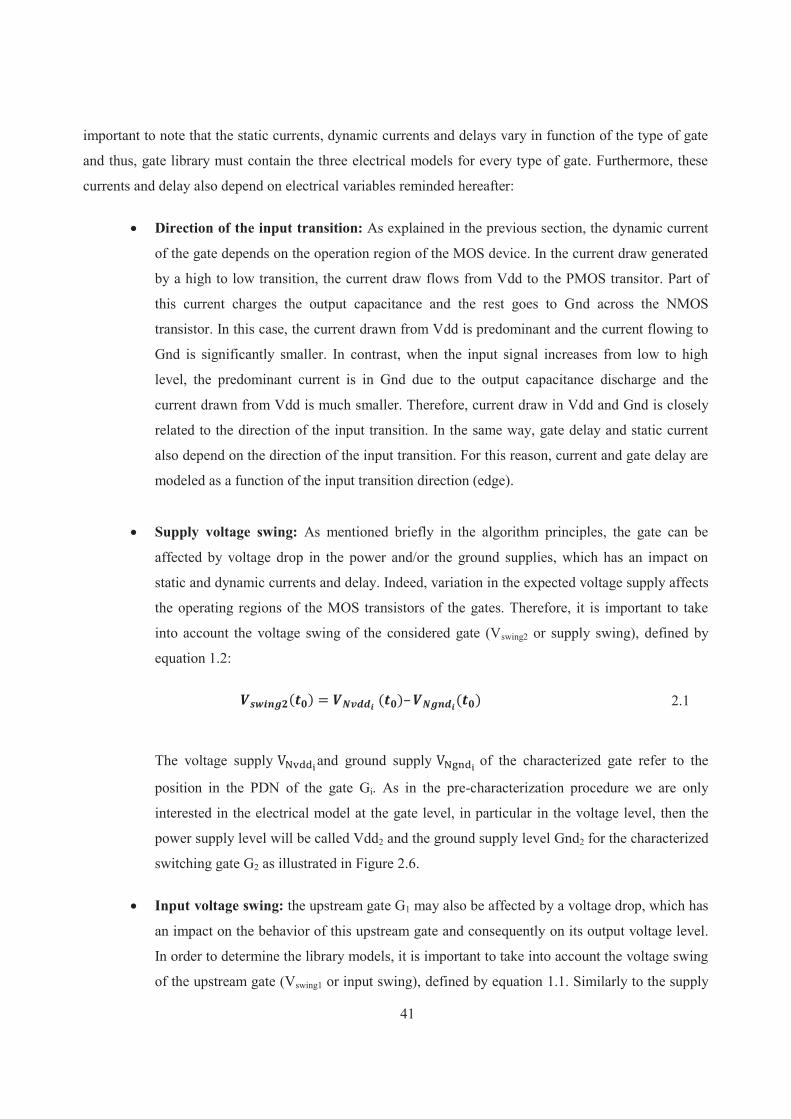
of the gate depends on the operation region of the MOS device. In the current draw generated
by a high to low transition, the current draw flows from Vdd to the PMOS transitor. Part of
this current charges the output capacitance and the rest goes to Gnd across the NMOS
transistor. In this case, the current drawn from Vdd is predominant and the current flowing to
Gnd is significantly smaller. In contrast, when the input signal increases from low to high
level, the predominant current is in Gnd due to the output capacitance discharge and the
current drawn from Vdd is much smaller. Therefore, current draw in Vdd and Gnd is closely
related to the direction of the input transition. In the same way, gate delay and static current
also depend on the direction of the input transition. For this reason, current and gate delay are
modeled as a function of the input transition direction (edge).
· Supply voltage swing: As mentioned briefly in the algorithm principles, the gate can be
affected by voltage drop in the power and/or the ground supplies, which has an impact on
static and dynamic currents and delay. Indeed, variation in the expected voltage supply affects
the operating regions of the MOS transistors of the gates. Therefore, it is important to take
into account the voltage swing of the considered gate (Vswing2 or supply swing), defined by
equation 1.2:
2.1
The voltage supply and ground supply of the characterized gate refer to the
position in the PDN of the gate Gi. As in the pre-characterization procedure we are only
interested in the electrical model at the gate level, in particular in the voltage level, then the
power supply level will be called Vdd2 and the ground supply level Gnd2 for the characterized
switching gate G2 as illustrated in Figure 2.6.
· Input voltage swing: the upstream gate G1 may also be affected by a voltage drop, which has
an impact on the behavior of this upstream gate and consequently on its output voltage level.
In order to determine the library models, it is important to take into account the voltage swing
of the upstream gate (Vswing1 or input swing), defined by equation 1.1. Similarly to the supply

42
voltage swing, Vdd1 and Gnd1 are the power supply and ground supply levels of the upstream
gate G1 in the pre-characterization.
Vdd2 Vdd1
Gnd1 Gnd2
Vinput
Voutput
Vdd1
Gnd1 Gnd2
Vdd2
Equivalent
Cload
G1 G2
Figure 2.6: Library variable parameters definition
· Load capacitance: Gate G2 output is connected to downstream gates (fanout). These gates
have an intrinsic input capacitance, which is charged and discharged during the switching
process. Therefore, the output capacitance of the gate has an impact on the current draw and
gate delay. For the model procedure, an equivalent capacitance of the downstream gates Cload
is connected to the characterized gate.
The gate library therefore includes the current and delay models derived from electrical simulation.
The current and delay models are computed according to the above listed parameters:
d = (G, edge, Vswing1, Vswing2, Cload)
= (G, edge, Vswing1, Vswing2, Cload)
= (G, edge, Vswing1, Vswing2, Cload)
= (G, edge, Vswing1, Vswing2)
= (G, edge, Vswing1, Vswing2)
Note that static currents do not depend on the load capacitance in the above equations. This is because
there is no charge and discharge activity in the output capacitance when a gate does not switch and thus,
static currents are independent of the load capacitance.
2.3 Library pre-characterization
During the pre-characterization process for a given technology, SPICE simulations are performed to
pre-characterize the dynamic current, the static current and the gate delay of every standard gate under all

43
the conditions that are likely to exist in a realistic environment. A standard electrical configuration,
illustrated in Figure 2.7, is used to simulate all the library gates with all the possible combinations of the
electrical parameters. To make the input transition generation more realistic, a traditional pulse voltage
source is connected to an inverter, which creates a realistic signal in terms of rise and fall times. Both
elements are supplied with nominal voltage for Vdd and Gnd called Vddn and Gndn. The output signal of
the auxiliary inverter is connected to a controlled voltage source. This controlled voltage source does not
apply a modification to the voltage level of the output. Its role is only to filter all the spurious variations
resulting from the ideal pulse voltage source.
Vddn
Cload
Inv Inv Inv
+
-
-
Gndn
Vdd1 Vdd2
Gnd1 Gnd2 Vinput
Characterized gate
+
VVddn
Gndn
Vddn
Gndn Gnd1
VddVdd1
Figure 2.7: Pre-characterization electrical schematic for an inverter
Once the input signal for the circuit has been defined, an upstream gate is attached to the
characterized gate. In the standard model, an inverter is used as upstream gate to model the voltage supply
swing of the characterized gate input. Finally, the output of the characterized gate is connected to a load
capacitance that represents the fanout of the characterized gate. The proposed pre-characterization
schematic provides an accurate electrical configuration for SPICE simulations of all possible
combinations of Vswing1, Vswing2 and load capacitance Cload.
The voltage swings Vswing1 and Vswing2 vary from 100% to 80% of the nominal power supply. The
voltage supply levels applied to the bias of the characterized gate (Vdd2 and Gnd2) and to the bias of the
upstream inverter (Vdd1 and Gnd1) are constant in time and symmetrical. Therefore, if a voltage supply
swing of 80% of the nominal one is applied to a characterized gate, the voltage supply Gnd2 will be 10%
of the nominal power supply and the voltage supply Vdd2 will be 90% of the nominal power supply. From
now on, we define Vswing1 and Vswing2 in percentage of the nominal power supply Vnominal as expressed in
equations 2.1and 2.3.
2.2

44
2.3
Concerning the load capacitance, the pre-characterization process applies discrete variations of its
value between one Cmin and five Cmin, where Cmin is the equivalent input capacitance of an elementary
inverter. All possible combinations of Vswing1, Vswing2 and load capacitance Cload are simulated using SPICE
for every gate in the pre-characterization procedure. As a result, a model can be derived from these
electrical simulations to compute the current draw, quiescent current and gate delay based on any
electrical configuration. The gate library contains electrical models for the following types of gate:
inverter, NAND2, NOR2, NAND3, NOR3, NAND4, NOR4 and buffer. In the following subsections, the
pre-characterization procedure for every library element is explained in detail.
2.3.1 Delay model
The conventional definition of the propagation delay δ is the amount of time between the input signal
of the gate crossing half of its excursion (Vnominal/2 in an ideal case without IR drop) and the output signal
of the gate crossing half of its excursion.
In the pre-characterization procedure, SPICE simulations are performed with different supply and
input swings (Vswing2 and Vswing1 respectively). As supply and input voltage swings can be different, the
propagation delay δ is defined as the duration between the time t0 at which the input signal of the gate
crosses half of its specific excursion Vswing1/2 and the time t1 at which the output signal of the gate crosses
half of its specific excursion Vswing2/2, as illustrated in Figure 2.8.

45
Time
Vdd1
Vdd2
Vddn
Gnd1
Gndn
Gnd2 V
sw
ing
2
Vs
win
g1
δ
t0 t1
Voutput
Vinput
Voltage
Vswing2 /2
Vswing1 /2
Vdd2 Vdd1
Gnd1 Gnd2
Vinput
Voutput
Vdd1
Gnd1 Gnd2
Vdd2
Equivalent
Cload
Figure 2.8: Library electrical parameters definition
Note that the nominal delay δnom of a gate can be obtained with ideal voltage supplies Vswing1=Vnominal
and Vswing2=Vnominal. For example, in the 45nm technology used here, the nominal delay is δnom=4.903ps for
an inverter controlled by a high to low transition.
The delay increases linearly when the voltage swing Vswing2 of the gate decreases, the other parameters
being constant at their nominal value, for a positive input transition, as illustrated in Figure 2.9.b. It also
increases when the input swing Vswing1 decreases. This latter dependence is slightly less linear, but it can
be approximately defined by a straight line with an average error inferior to 0.5%, as respresented in
Figure 2.9.a. Although the delay with varying load capacitance describes an exponential curve, this curve
can be approximated by a linear function if the load capacitance variation stays in a small range from one
to five times Cmin, as shown in Figure 2.9.c.

46
Figure 2.9: Inverter delay variations in function of voltage swings and load capacitance
The three varying parameters are dependent and consequently the effect of one variable on the delay
depends on the value of the other two variables, i.e. an additive Multiple-Linear Regression (MLR)
equation with multiplicative interactions can be used for each parameter and also for the combination of
the variables in order to model the gate delay. Therefore an additive MLR equation of the delay is
established as a function of Vswing1, Vswing2 and load capacitance Cload. This MLR equation depends on the
direction of the input transition (rising or falling) and the gate type (e.g. inverter, NAND2). Consequently,
two sets of 8 regression coefficients are given to the simulator to compute the delay for each gate type as
shown by equations 2.4(rising edge) and 2.5(falling edge):
d
2.4
d
2.5
where a0, b0, c0, d0, e0, f0 , g0, h0 are the coefficients associated to the delay of the inverter for a rising
transition (d0_1) and a1, b1, c1, d1, e1, f1, g1, h1 are the coefficients of the delay for a falling transition (d1_0).
The two sets of coefficients associated to the inverter are given in Table 2.2.

47
Table 2.2: Regression coefficients for the delay computation of an inverter.
ai bi ci di ei fi gi hi
δ0_1 (10-12
) 14.295 -9.656 -8.160 5.999 6.746 -2.750 -4.162 2.600
δ1_0 (10-12
) 13.479 -9.337 -6.427 5.583 5.185 -3.395 -4.203 3.113
Figure 2.10 shows the delay variation for an inverter controlled by a positive input transition as a
function of the input and power swings with minimal load capacitance obtained from SPICE simulation
(left graphic) and from the MLR model (right graphic). Average relative error is a faithful way to measure
the accuracy of the model because relative error is high only in the front corner case, i.e. the worst relative
error is 1.06% for a 20% of voltage supply drop in the upstream gate and the characterized gate. But a
voltage supply drop of more than 10% is extremely improbable. However, over the full range of swing
corresponding to 20% of the drop, the average error when estimating delay is 0.56%. Overall, including
variations in the load capacitance, the average error is as low as 0.35%. The average error is very
satisfactory compared to other studies on the topic [9].
Figure 2.10: Variation of the delay as a function of Vswing1 and Vswing2 with Cmin load obtained from Spice simulation (left)
and computed from MLR function (right).
To determine the overall precision of the model, the worst relative error and the average relative error
are computed for every library gate. For the considered 45nm technology, Table 2.3 shows the estimation
errors. As illustrated with the above inverter example, the relative error can be high in the corner case, but
it is not representative of the simulation error for the delay model. The worst relative error in delay

48
estimation is 5% for the buffer gate. The average relative error is as low as 1.75% for the same gate. In
brief, the obtained results look very satisfactory for all characterized gates and the suggested electrical
model provides an accurate model to estimate the induced gate delay in function of the electrical
parameters previously described.
Table 2.3: Delay model error.
Gate Input vector Switching input Worst relative error (%) Average relative error (%)
INV 0/ 1 Input 1: Rising edge 1.2324 0.3561
INV 1/0 Input 1: Falling edge 1.8228 0.6020
BUF 0/1 Input 1: Rising edge 5.0439 1.7582
BUF 1/1 Input 1: Falling edge 2.9783 0.5406
NAND4 0111/1111 Input 1: Rising edge 2.2225 0.5187
NAND3 011/111 Input 1: Rising edge 2.1956 0.4758
NAND2 01/11 Input 1: Rising edge 1.5358 0.3634
NAND4 1111/0111 Input 1: Falling edge 2.3041 0.4827
NAND3 111/011 Input 1: Falling edge 2.1057 0.4800
NAND2 11/01 Input 1: Falling edge 2.4156 0.4793
NAND4 1011/1111 Input 2: Rising edge 3.7521 0.5336
NAND3 101/111 Input 2: Rising edge 1.9149 0.4287
NAND2 10/11 Input 2: Rising edge 1.5917 0.3710
NAND4 1111/1011 Input 2: Falling edge 1.6869 0.3387
NAND3 111/101 Input 2: Falling edge 1.5810 0.3537
NAND2 11/10 Input 2: Falling edge 1.7089 0.3707
NAND4 1101/1111 Input 3: Rising edge 2.1284 0.5305
NAND3 110/111 Input 3: Rising edge 2.1805 0.4393
NAND4 1111/1101 Input 3: Falling edge 2.4785 0.3559
NAND3 111/110 Input 3: Falling edge 1.5927 0.3027
NAND4 1110/1111 Input 4: Rising edge 2.7773 0.5744
NAND4 1111/1110 Input 4: Falling edge 1.4083 0.3398
NOR4 0010/0000 Input 3: Falling edge 2.7397 0.6070
NOR4 0000/0010 Input 3: Rising edge 1.1659 0.2817
NOR4 0000/0001 Input 4: Rising edge 1.2701 0.2977
NOR4 0001/0000 Input 4: Falling edge 3.1232 0.6967
NOR3 000/001 Input 3: Rising edge 1.2246 0.3148
NOR3 001/000 Input 3: Falling edge 2.6132 0.5666
NOR4 0000/0100 Input 2: Rising edge 1.1202 0.3557

49
NOR3 000/010 Input 2: Rising edge 1.1930 0.2913
NOR2 00/01 Input 2: Rising edge 1.2475 0.3291
NOR4 0100/0000 Input 2: Falling edge 2.2522 0.4842
NOR3 010/000 Input 2: Falling edge 2.5316 0.5631
NOR2 01/00 Input 2: Falling edge 2.7057 0.5557
NOR4 0000/1000 Input 1: Rising edge 1.1450 0.4695
NOR3 000/100 Input 1: Rising edge 1.1902 0.3840
NOR2 00/10 Input 1: Rising edge 1.1788 0.2982
NOR4 1000/0000 Input 1: Falling edge 2.0635 0.3988
NOR3 100/000 Input 1: Falling edge 2.0773 0.4763
NOR2 10/00 Input 1: Falling edge 1.9369 0.4637
2.3.2 Dynamic current model
As previously mentioned, the current drawn by a switching gate from the power and ground supplies
is a time variant function. Therefore, the electrical model for the dynamic current cannot be a single value.
For this reason, the current draw is modeled as an array of values as illustrated in Figure 2.11. For the sake
of simplicity, from now on we consider a convention with positive currents getting into the gate, i.e. the
current flow is considered positive from the supply to the gate whatever the considered supply. As a result,
the current Ignd from the ground supply to the gate is presented as positive, although it actually flows in the
opposite direction as previously illustrated in Figure 2.3.
0 1 2 4 6 8 10 Time (ps)
Istatic_vdd
Istatic_gnd
3 5 109 10 11
Istatic_vdd vdd Istatic_gnd
100 points =
100 ps
Cu
rren
t (
A)
Figure 2.11: Dynamic current model arrays
The reference current draw, corresponding to the current draw induced by the switching gate under
nominal electrical conditions, is thus stored as an array of 100 current amplitude values with picosecond
resolution. From this reference, the actual current draw can be computed according to environmental

50
conditions. The first point of the array corresponds to t0 in Figure 2.8. Note that it is sure that the current
draw will fall back to zero in less than 100ps whatever the conditions, so our 100 point table is large
enough. When a gate is switching, the current drawn from Vdd is different from the current drawn from
Gnd (see section 2.2) and so two reference arrays must therefore be used: Ivdd and Ignd.
Figure 2.12: Variation of the transient current draw for different values of a)the power swing; b) the input swing; c) the
load capacitance
Figure 2.12 shows the transient current drawn from the ground supply during the switching of an
inverter controlled by a positive transition (in this case, this is the predominant current draw). Figure 2.12.a
gives the current draw obtained by SPICE simulation for different values of the gate power swing Vswing2,
Figure 2.12.b for different values of the input swing Vswing1 and Figure 2.12.c for different values of the
load capacitance Cload. Note that only one parameter varies at a time while the two other parameters are kept
constant at nominal value (Vswing1,2=100% of nominal voltage and Cload=Cmin). Considering a reference
curve with Vswing1=100%, Vswing2=100% and Cload=Cmin (in yellow on Figure 2.12.a and Figure 2.12.b, in
blue on Figure 2.12.c), the effect of the gate power swing Vswing2 on the transient current draw appears to be
a simple homothety of the amplitude. In this case, a single multiplying factor is thus sufficient to derive the
array of current values from the reference array. A similar amplitude effect can be observed on the current
draw when the input swing Vswing1 varies, but this is then associated with a shift in time. To derive the
actual current values from the reference, it is possible to shift the values in the array and then apply a
multiplying factor. The impact of the load capacitance on the current draw is significantly much more
difficult to model. No simple factor can be found to compute all the other curves from a reference curve.
However, because only five different values of the load capacitance are considered, it is possible to store

51
the corresponding five arrays of current values for a nominal input and power swings. It should be noted
that the results and conclusions for the current draw in the Vdd power supply are similar to those previously
presented for Gnd.
The average Normalized Root Mean Square Deviation (NRMSD) between the current draw
waveforms, sweeping all the possible combinations of Vswing1 and Vswing2, obtained by SPICE simulation on
the one hand and derived from the reference current arrays applying the adequate amplitude factor and time
shift is computed to determine the electrical model accuracy. Table 2.4 gives a representative extract of the
obtained NRMSD for different gates and input transitions. The complete table of NRMSD is available in
annex. The maximal average estimated error for all possible combinations of the electrical parameters is
5.19% in the case of an inverter. The error in this latter case is particularly high compared to the observed
results in the other cases. In general, the average error is close to 1% for a given gate and input transition
(the overall average error for all the logic gates and transitions is as low as 1.15%). Although these results
in terms of estimation error are worse than the ones obtained with the gate delay, it should be noted that an
array of values is much more complex to handle. In some papers the current draw is modeled as a simple
triangular function [3], [17] or as a trapezoidal function [2], [18], implying obviously some
approximations. Note that the estimation errors are not available in these publications but it is obvious that
this kind of approximation is less accurate than the suggested electrical model introduced in this section.
For this reason we can conclude that the suggested electrical model is accurate for the current draw
prediction.
Table 2.4: NRMSD of the current draw model (extract).
Gate Input vector Switching input Cload Current Vdd:
average NRMSD (%)
Current Gnd:
average NRMSD (%)
INV 0/ 1 In 1: Rising edge 5 Cmin 0.2375 5.1877
INV 1/0 In 1: Falling edge 5 Cmin 2.9270 0.1672
BUF 0/1 In 1: Rising edge 1 Cmin 1.6808 1.2412
BUF 1/1 In 1: Falling edge 1 Cmin 1.1576 1.2156
NAND4 0111/1111 In 1: Rising edge 2 Cmin 0.3366 1.130
NAND3 011/111 In 1: Rising edge 5 Cmin 0.3291 0.8893
NAND2 01/11 In 1: Rising edge 5 Cmin 0.3493 1.8745
NAND4 1111/0111 In 1: Falling edge 2 Cmin 1.9991 0.3448
NAND3 111/011 In 1: Falling edge 4 Cmin 2.3699 0.3614
NAND2 11/01 In 1: Falling edge 3 Cmin 1.0119 0.1953
NAND4 1011/1111 In 2: Rising edge 5 Cmin 0.4626 1.7695

52
NAND3 101/111 In 2: Rising edge 3 Cmin 0.4858 1.6074
NAND2 10/11 In 2: Rising edge 5 Cmin 1.2716 3.7823
NAND4 1111/1011 In 2: Falling edge 4 Cmin 0.8490 0.2203
NAND3 111/101 In 2: Falling edge 5 Cmin 0.6310 0.1742
NAND2 11/10 In 2: Falling edge 5 Cmin 0.6493 0.1789
NAND4 1101/1111 In 3: Rising edge 5 Cmin 2.3316 1.3808
NAND3 110/111 In 3: Rising edge 5 Cmin 1.9255 4.0419
NAND4 1111/1101 In 3: Falling edge 4 Cmin 0.4023 0.3691
NAND3 111/110 In 3: Falling edge 5 Cmin 0.6506 0.1567
NAND4 1110/1111 In 4: Rising edge 3 Cmin 3.0476 3.8167
NAND4 1111/1110 In 4: Falling edge 2 Cmin 1.5753 0.3529
NOR4 0010/0000 In 3: Falling edge 4 Cmin 0.4727 3.6431
NOR4 0000/0010 In 3: Rising edge 5 Cmin 1.2971 0.1897
NOR4 0000/0001 In 4: Rising edge 5 Cmin 0.4784 1.9594
NOR4 0001/0000 In 4: Falling edge 4 Cmin 1.7924 0.1654
NOR3 000/001 In 3: Rising edge 2 Cmin 0.1719 1.3203
NOR3 001/000 In 3: Falling edge 3 Cmin 0.4784 1.6886
NOR4 0000/0100 In 2: Rising edge 5 Cmin 0.3316 2.3088
NOR3 000/010 In 2: Rising edge 1 Cmin 1.4558 1.6867
NOR2 00/01 In 2: Rising edge 1 Cmin 2.3716 1.3795
NOR4 0100/0000 In 2: Falling edge 5 Cmin 1.9979 0.1527
NOR3 010/000 In 2: Falling edge 4 Cmin 0.2008 0.7838
NOR2 01/00 In 2: Falling edge 2 Cmin 0.1463 1.6658
NOR4 0000/1000 In 1: Rising edge 4 Cmin 0.5057 2.2549
NOR3 000/100 In 1: Rising edge 5 Cmin 3.3468 0.7776
NOR2 00/10 In 1: Rising edge 5 Cmin 2.4373 1.7666
NOR4 1000/0000 In 1: Falling edge 1 Cmin 3.1374 0.5565
NOR3 100/000 In 1: Falling edge 5 Cmin 0.4114 1.4539
NOR2 10/00 In 1: Falling edge 4 Cmin 2.8578 0.3560
2.3.3 Static current model
The static or quiescent current of a gate is defined in section 2.1. These undesirable currents are
generated by the parasitic elements of the MOS transistor. In past technologies the static currents were low
and neglected, but today technology scaling has increased the magnitude of the static current. Firstly, it is
necessary to determine whether the quiescent current can be neglected or has a significant impact on the
voltage drop in the PDN.
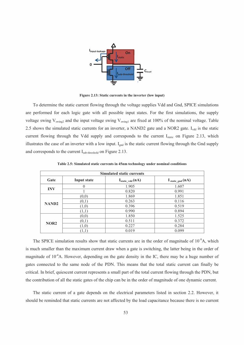
53
Isub-threshold
0
Cload
Istatic
Iinput-leakage On
Off
Figure 2.13: Static currents in the inverter (low input)
To determine the static current flowing through the voltage supplies Vdd and Gnd, SPICE simulations
are performed for each logic gate with all possible input states. For the first simulations, the supply
voltage swing Vswing2 and the input voltage swing Vswing1 are fixed at 100% of the nominal voltage. Table
2.5 shows the simulated static currents for an inverter, a NAND2 gate and a NOR2 gate. Ivdd is the static
current flowing through the Vdd supply and corresponds to the current Istatic on Figure 2.13, which
illustrates the case of an inverter with a low input. Ignd is the static current flowing through the Gnd supply
and corresponds to the current Isub-threshold on Figure 2.13.
Table 2.5: Simulated static currents in 45nm technology under nominal conditions
Simulated static currents
Gate Input state Istatic_vdd (nA) I static_gnd (nA)
INV 0 1.905 1.607
1 0.820 0.991
NAND2
(0,0) 1.869 1.851
(0,1) 0.263 0.116
(1,0) 0.396 0.519
(1,1) 0.990 0.894
NOR2
(0,0) 1.850 1.525
(0,1) 0.511 0.372
(1,0) 0.227 0.284
(1,1) 0.019 0.099
The SPICE simulation results show that static currents are in the order of magnitude of 10-9
A, which
is much smaller than the maximum current draw when a gate is switching, the latter being in the order of
magnitude of 10-4
A. However, depending on the gate density in the IC, there may be a huge number of
gates connected to the same node of the PDN. This means that the total static current can finally be
critical. In brief, quiescent current represents a small part of the total current flowing through the PDN, but
the contribution of all the static gates of the chip can be in the order of magnitude of one dynamic current.
The static current of a gate depends on the electrical parameters listed in section 2.2. However, it
should be reminded that static currents are not affected by the load capacitance because there is no current

54
spread from the gate to the output terminal in a non-switching gate. On the contrary, the static current
appears when the input state is stable and so this current depends on the input swing Vswing1. Naturally, the
amount of static current flowing from Vdd to Gnd also depends on the power swing Vswing2.
Figure 2.14 shows the static current evolution for an inverter gate depending on the input voltage Vinput
and the supply voltage swing Vswing2. Note that the supply voltage swing is applied symmetrically in the
pre-characterization schematic. As the nominal supply voltage for 45nm technology is 1V, when the input
voltage swing is 80% of the nominal supply voltage, Vinput is 0.1V if the logic input is 0, and 0.9V if the
logic input is 1. As far as static currents in Vdd have a very similar behavior when the voltage swings
vary, we focus only on the current in Vdd in the next paragraph. Of course, similar projections are
observed for the current in Gnd.
Figure 2.14: Static current of an inverter in function of Vinput and Vswing2
The obtained static current values are plotted in Figure 2.15 for different combinations of Vinput and
Vswing2. Regarding the static current dependency on supply voltage, it can be concluded that:
· The static current of a gate exponentially decreases with the gate supply voltage swing Vswing2.
In other words, the higher the IR-drop effect on the supply of the gate, the smaller its static

55
current. Indeed, when the supply swing is smaller, the difference of potential is smaller and
therefore the current flowing from the power supply to the ground is smaller.
· The static current of a gate exponentially increases when the gate input voltage swing Vswing1
decreases. This means that the static current of an inverter with a low input increases when
Vinput increased and the static current of an inverter with a high input increases when Vinput
decreases. Indeed, when the input voltage swing is smaller, the input voltage level approach to
the noise margins of the gate and thus, transistor in the cut-off operating region (NMOS for a
low input and PMOS for a high input) allows to conduct more current.
Figure 2.15: Static current in Vdd of an inverter in function of Vinput and Vswing2
Concerning the IR-Drop simulation, we consider that a large number of gates are connected to the
same node in the PDN model. All the gates connected to the same node are affected by the same supply
voltage drop and therefore the output voltage of these gates is affected by the same voltage drop. Because
of the physical connectivity most of the gates are connected to the same node as their upstream gates.

56
Therefore, generally the input voltage swing Vswing1 and the supply voltage swing Vswing2 are equal for the
static current computed by the simulator. This enables a simplification of the static current model using
Vswing1=Vswing2. Figure 2.16 shows the static current function using this simplified model for an inverter.
Figure 2.16: Static current of an inverter when Vswing1 = Vswing2
2.4 Pre-characterization constraints
The pre-characterization procedure for the gate delay and current draw provides a model that is valid
for a wide range of combinations of the electrical parameters. Indeed, SPICE pre-characterization
simulations are performed under all the conditions that are likely to exist in a realistic environment. But of
course, there are some limitations concerning the accuracy of this model.
During the pre-characterization, dynamic currents, static currents and delays are derived from SPICE
simulations for different values of input voltage swing Vswing1, supply voltage swing Vswing2 and load
capacitance Cload. When a gate switches, the input voltage swing and the supply voltage swing of the gate
evolve in the time, changing their levels during the commutation time due to the switching activity of the
neighboring gates. Therefore, there is an infinity of different possibilities that pre-characterization
procedure cannot take into account for the modeling. For this reason, the pre-characterization procedure
considers only stable levels of input voltage swing and the supply voltage swing.
Another limitation of the model refers to the considered fanout. The discretization of the load
capacitance to Cmin multiples is necessary to define the current draw models. Obviously, the input
capacitance of a gate is Cmin only for the inverters. For rest of the standard gates the input capacitance is

57
higher than Cmin. It means that the computed load capacitor is always smaller than or equal to the real load
capacitance.
The pre-characterization simulations for each logic gate only include single input switching
conditions, not simultaneous switchings of different inputs of the same gate. In the case of simultaneous
switchings of a gate inputs, the current draw and the delay of the gate depend on both input transitions.
The actual resulting current draw and delay is not a simple combination of both transitions considered
independently. A similar observation can be made when different inputs of the same gate switch
successively in a small slice of time (typically smaller than the gate delay). In these cases, the exhaustive
characterization of the delay and the current draw is not feasible because there is an infinity of possible
combinations of input events during a gate commutation delay. In brief, the electrical model provided by
the pre-characterization library is imprecise in these cases. Fortunately, the probability of simultaneous
switching events is small and in addition their impact is limited due to the modest impact of a single
current draw generated by a switching gate in comparison with the global current that flows through the
whole chip.
2.5 Self IR-Drop
In the pre-characterization procedure, SPICE simulations are performed for different supply voltage
swings Vswing2 but the pre-characterization procedure does not take into account the supply voltage
variation generated by the switching gate itself. We call this phenomenon self-IR-Drop. Although self-IR-
Drop is an electrical effect at the gate level, it also depends on the resistive elements of the PDN.
The aim of this section is to evaluate the impact of self-IR-Drop on the current draw and delay of the
gate. To do so, a new electrical schematic is simulated with SPICE; this schematic must include a resistive
PDN model between the voltage supply Vdd and the power bia connection and other one between the
ground supply Gnd and the ground bia connection. As the current distribution through the PDN is
irrelevant, an equivalent resistance of the resistive grid can be used (Rg_vdd_eq for the power grid and
Rg_gnd_eq for the ground grid). Resistive grid and its equivalent resistance are explained with more details in
section 3.1. The equivalent grid resistance is connected between the power supply Vdd (resp. ground
supply Gnd) and the power bia connection nvdd_supply (resp. ground bia connection ngnd_supply) of the gate as
illustrated in Figure 2.17.

58
G
Cload
Rg_vdd_eq
Rg_gnd_eq
ngnd_supply
nvdd_supply
Figure 2.17: Schematic for self-IR-Drop simulation
Our expectation is that self-IR-Drop is negligible because the current draw generated by a gate is
approximately 10-4
A. Therefore, using a realistic value for the equivalent grid resistance around 1Ω, the
self-IR-Drop voltage drop at the supply voltage connection of the gate will be negligible. To confirm this
hypothesis a simulation with an inverter is performed. The supply voltage swing Vswing2 and the input
voltage swing Vswing1 of the inverter are fixed at 100% of the nominal voltage. To create a realistic
environment, equivalent grid resistance values between 0Ω and 1Ω are simulated (see 3.1.2.4).
Once the electrical parameters have been defined, the impact of the self-IR-Drop is evaluated. The
current draws and gate delays gotten from the SPICE simulations with and without the equivalent grid
resistance in Vdd and Gnd are compared. Figure 2.18 shows the SPICE results when the inverter input
switches from low to high. In the plotted results, the equivalent grid resistor used to model the Vdd PDN
and the equivalent grid resistor used to model the Gnd PND have the same value R_eq which varies from
0Ω to 1Ω. We observe for example the current and voltage in the Gnd node ngnd_supply: the current draw
variation is slight. In addition, the voltage drop in Gnd node is approximately 10-4
V for the worst case
corresponding to Rg_eq = 1Ω.

59
Figure 2.18: Self IR-Drop simulation of an inverter
In conclusion, when the self-IR-Drop effect is omitted in the pre-characterization procedure, the
maximal error in delay estimation is 0.018%. For the current draw, the maximal error is 0.020%.
Therefore, self-IR-Drop impact is negligible due to the low voltage drop generated by the characterized
gate switching itself and can indeed be neglected during the pre-characterization procedure.

60

61
3 Electrical model of the PDN current distribution
As described in the first chapter, an IR-Drop simulation requires by definition a model for the current
‘I’ and a model for the resistance ‘R’. In the previous chapter, an electrical model has been defined for
dynamic and static currents in the frame of the pre-characterization procedure. In this chapter, the current
distribution through the PDN needs to be analyzed as a function of the resistance ‘R’ of the PDN, i.e. an
electrical model for the PDN must be proposed in order to determine the current distribution through the
PDN.
As explained in section 1.1, IR-Drop is an electrical phenomenon that dissipates in space. Hence, the
current distribution through the PDN generated by a current draw causes a voltage drop in the area
neighboring the switching gate. Far from the switching gate, the impact of the current draw is negligible.
Consequently, in order to reduce the simulation time, the simulator only computes the current distribution
in the neighborhood of the gate. This area is called the current window and the main objective of this
chapter is to accurately determine the current into the considered current window.
It is important to note that the current distribution through the PDN is closely related to the electrical
model used for the PDN. For this reason, the electrical model of the PDN must be carefully determined.
We consider two different electrical models for the PDN and this chapter is consequently structured into
two main sections:
· In the first section, the current distribution is analyzed using a purely resistive model for PDN
grid.
· In the second one, the presence of capacitive elements in the PDN is studied and an electrical
model of the PDN including capacitive elements is suggested.

62
3.1 Electrical model for the current distribution in a resistive grid
3.1.1 PDN resistive model
As explained in section 1.4, on-chip parasitic elements of the PDN imply that the PDN can be
modeled as a conductive grid with resistive, inductive and capacitive parasitic elements. This electrical
model of the PDN is used by the simulator to compute the current distribution and calculate the voltage
drop in every node. Consequently, it is necessary to use an accurate PDN model in order to implement an
IR-Drop induced delay simulator.
IR-Drop is defined as an electrical phenomenon that mainly concerns the resistive elements of the
PDN and the current that flows through these resistive elements. Naturally, the current distribution also
depends on the capacitive and inductive elements, but these ones have a low impact in comparison with
the resistive ones. Indeed, the resistance is the dominant on-chip parasitic element of the PDN. In this first
approach of the IR-Drop phenomenon, the capacitive and inductive elements of the PDN are not
considered and so, the electrical model exclusively tackles the resistive elements and their impact on the
current distribution.
Therefore, the PDN is modeled as a two-dimensional resistive grid NgxMg as described in section 1.4.
The value of each resistor depends on the PDN topology, the technology and the types of metal in the
PDN. For the high metal levels the PDN topology is regular. For the low metal level, wires and vias are
placed irregularly, but these wires are used for short local connections. For this reason, the parasitic
resistance at the low metal level is negligible. Consequently, only the high metal levels with a regular grid
structure are taken into account for the electrical model. In addition, it is usual to simplify the PDN model
by assuming that horizontal resistors are all equal to each other and vertical resistors are also all identical
to each other.
These horizontal and vertical resistor values are computed using design commercial tools based on the
extracted resistance values from the PDN metal levels. Hence, a resistive grid with an elementary
horizontal resistance rh and an elementary vertical resistance rv is suggested as an electrical model for the
PDN as illustrated in Figure 3.1.a for a 4x4 grid example.

63
Figure 3.1: PDN resistive model
For the sake of simplicity, the resistive grid is illustrated in the rest of this document by a simple grid
where segments implicitly represent the different resistances as shown in Figure 3.1.b. The nodes through
the symbolic resistive grid are illustrated in Figure 3.2.a. Every resistor of the PDN grid is associated to a
current and thus, currents across the different segments of the symbolic grid represent currents across the
resistive elements. The currents across vertical resistors Iv(i,j) and the currents across horizontal resistors
Ih(i,j) with their corresponding names are illustrated in Figure 3.2.b.
Figure 3.2: Currents and nodes in the symbolic grid
a) Resistive grid b) Symbolic grid
Rh(1,1) Rh(1,2) Rh(1,3) Rh(1,4)
Rh(2,1) Rh(2,2) Rh(2,3) Rh(2,4)
Rh(3,1) Rh(3,2) Rh(3,3) Rh(3,4)
Rh(4,1) Rh(4,2) Rh(4,3) Rh(4,4)
Rh(5,1) Rh(5,2) Rh(5,3) Rh(5,4)
Rh(1,1) Rh(1,2) Rh(1,3) Rh(1,4)
Rh(2,1) Rh(2,2) Rh(2,3) Rh(2,4)
Rh(3,1) Rh(3,2) Rh(3,3) Rh(3,4)
Rh(4,1) Rh(4,2) Rh(4,3) Rh(4,4)
Rh(5,1) Rh(5,2) Rh(5,3) Rh(5,4)
Rv(1
,1)
Rv(2
,1)
Rv(3
,1)
Rv(4
,1)
(1,1)
Rv(1
,2)
(2,1)
Rv(2
,2)
(3,1)
Rv(3
,2)
(4,1)
Rv(4
,2)
(1,2)
Rv(1
,3)
(2,2)
Rv(2
,3)
(3,2)
Rv(3
,3)
(4,2)
Rv(4
,3)
(1,3)
Rv(1
,4)
(2,3)
Rv(2
,4)
(3,3)
Rv(3
,4)
(4,3)
Rv(4
,4)
(1,4)
Rv(1
,5)
(2,4)
Rv(2
,5)
(3,4)
Rv(3
,5)
(4,4)
Rv(4
,5)
Rv(1
,1)
Rv(2
,1)
Rv(3
,1)
Rv(4
,1)
1) R
Rv(1
,2)
(2,1) R
Rv(2
,2)
(3,1) R
Rv(3
,2)
1) R
Rv(4
,2)
(1,2) R
Rv(1
,3)
(2,2) R
Rv(2
,3)
(3,2) R
Rv(3
,3)
(4,2) R
Rv(4
,3)
(1,3) R
Rv(1
,4)
(2,3)
Rv(2
,4)
(3,3) R
Rv(3
,4)
(4,3) R
Rv(4
,4)
(1,4)
Rv(1
,5)
(2,4)
Rv(2
,5)
(3,4)
Rv(3
,5)
(4,4)
Rv(4
,5)
n(2,2)
n(3,2)
n(1,2)
n(2,1)
n(n(1,1)
n(3,1)
n(1,3)
n(2,3)
n(3,3)
a) Nodes in the symbolic grid b) Currents in the symbolic grid
n(4,1) n(4,2) n(4,3)
n(1,4)
n(2,4)
n(3,4)
n(4,4)
n(1,5)
n(2,5)
n(3,5)
n(4,5)
n(5,1) n(5,2) n(5,3) n(5,5) n(n(5,4)
Ih(1,1) Ih(1,2) Ih(1,3) Ih(1,4)
Ih(2,1) Ih(2,2) Ih(2,3) Ih(2,4)
Ih(3,1) Ih(3,2) Ih(3,3) Ih(3,4)
Ih(4,1) Ih(4,2) Ih(4,3) Ih(4,4)
Ih(5,1) Ih(5,2) Ih(5,3) Ih(5,4)
I v(1
,1)
I v(2
,1)
I v(3
,1)
I v(4
,1)
1)
I v(1
,2)
1)
I v(2
,2)
1)
I v(3
,2)
1)
I v(4
,2)
2) I
I v(1
,3)
2)
I v(2
,3)
2)
I v(3
,3)
2)
I v(4
,3)
3) I
I v(1
,4)
,3)
I v(2
,4)
3) I
I v(3
,4)
3) I
I v(4
,4)
4)I v
(1,5
)
4)
I v(2
,5)
4)
I v(3
,5)
4)
I v(4
,5)

64
3.1.2 The distribution factor
During simulation, the current drawn by a gate is first obtained from the pre-characterized library and
then needs to be propagated through the whole PDN. In other words, different fractions of this ‘original’
current flow through the different resistors of the PDN. It is therefore necessary to determine the fraction
of current in each resistance of the PDN. Although the ideal method would be to mathematically compute
the current fractions, the grid topology makes it difficult to find a simple and efficient equation. For this
reason, mathematical computation is dismissed and the current fractions are determined from a simple pre-
characterization of the grid using SPICE.
The pre-characterization procedure consists in determining a distribution factor that corresponds to the
percentage of the current draw flowing in each branch of the PDN grid. We consider a gate connected to
the node n(i,j) of the resistive NgxMg grid whose edge is connected to the nominal supply voltage Vdd. As
explained in the previous section, the current draw I of the gate spreads through the PDN as illustrated in
Figure 3.3.a. Obviously, the current distribution through the PDN is a function of the current I drawn by
the gate and the values rv and rh. The pre-characterization procedure is illustrated hereafter in the case of
the power PDN. Obviously, the same approach can be conducted for the ground PDN with similar
conclusions. When both grids have the same characteristics in terms of rh and rv, the same distribution
factor can be used for both grids.
VDD
I(i,j)
VDD
VDD
VDD
VDD
VDD
VDD VDD
VDD
VD
VDD
VDD
VDD
VDD VDD
VDD
(i,j)VDD VDDVDD
VDD D
VDD
VDD
D
VDD
Iv(i,j) Ih(i,j) I (i,j,j)
n(i,j)
VDD
Is
VDD
VDD
VDD
VDD
VDD
VDD VDD
VDD
VD
VDD
VDD
VDD
VDD VDD
VDD
I
VDD VDD
VDD D
VDD
VDD
D
VDD
dfv(i,j) dfh(i,j
)
df (i(i,j
n(i,j)
a) Current distribution b) Distribution factor
Figure 3.3: Example of SPICE simulations to determine the distribution factor

65
Regarding the current distribution through the NgxMg grid, we can associate a ratio to every horizontal
and vertical resistor. This ratio determines the relation between the current draw and the current across the
resistor:
3.1
For a different current draw, the ratio is defined as:
3.2
The current across every resistive element is directly proportional to the current draw but as the
current spreads through a resistive grid, the ratio of every resistor is independent of the current draw and
constant. Therefore, the ratio associated to a resistor is equal even for different values of current draw.
3.3
Based on this property, if the current draw I is modeled as a unitary current source Is=I=1 connected to
the node n(i,j) (as illustrated in Figure 3.3.b), the current flowing in each branch of the resistive grid
corresponds directly to the ratio of the corresponding resistor.
3.4
Once known the ratio for every resistor, the current through every resistor of the grid can be estimated
whatever the current draw. The ratio is referred to as the distribution factor df(i,j) in the rest of the
document.

66
3.5
3.6
Figure 3.4 shows the current distribution generated by a unitary source of current connected to the
central node of a 4x4 resistive grid. These currents are therefore the distribution factors. The results are
stored in two matrixes: horizontal currents are stored in the horizontal distribution factor matrix DFh and
vertical currents in the vertical distribution factor matrix DFV, as illustrated in Figure 3.4.
I v(3
,3)
Ih(3,3)
I v(2
,3)
I v(1
,3)
I v(4
,3)
I v(3
,2)
I v(2
,2)
I v(1
,2)
I v(4
,2)
I v(3
,4)
I v(2
,4)
I v(1
,4)
I v(4
,4)
Ih(3,2) Ih(3,1) Ih(3,4)
Ih(2,3)
)
Ih(2,2) Ih(2,1) Ih(2,4)
Ih(4,3) Ih(4,2) Ih(4,1) Ih(4,4)
4x4 Grid
Ih(2,1)
Ih(3,1)
Ih(4,1)
Ih(2,2)
Ih(3,2)
Ih(4,2)
Ih(2,3)
Ih(3,3)
Ih(4,3)
Ih(2,4)
Ih(3,4)
Ih(4,4)
Iv(2,2)
Iv(3,2)
Iv(4,2)
Iv(2,3)
Iv(3,3)
Iv(4,3)
Iv(2,4)
Iv(3,4)
Iv(4,4)
Iv(1,4) Iv(1,3) Iv(1,2)
DFv : 4x3 matrix
DFh : 3x4 matrix VDD
Figure 3.4: Distribution factor matrixes
Note that the distribution factor matrixes have different sizes: for a NgXMg resistive grid, the
horizontal distribution factor matrix is a (Ng-1)xMg matrix while the vertical distribution factor matrix is a
Ngx(Mg-1) matrix.
The distribution factor depends on the position of the gate in the PDN grid. Computing the
distribution factors for every node of the PDN is not efficient and so, a simplification is proposed in the
following subsections. For this simplification it is important to remember that the goal is to compute the
voltage drop in every node of the PDN during simulation with an acceptable accuracy. Therefore, the
distribution factor must just guarantee an error in the simulated current of the PDN branches inferior to
1%. The suggested current window must also be large enough to contain all current fractions higher than
1%.

67
3.1.2.1 Central model
The aim of the first pre-characterization simulation is to determine the current distribution when the
gate is connected in the central area of the PDN. As explained in the previous section, a SPICE simulation
is performed with the current draw modeled by a unitary current source in the center of the grid. For
example, Figure 3.5 shows the current distribution using a 100x100 resistive grid with horizontal and
vertical resistors of 0.4Ω [28] and whose edge is connected to the nominal power supply. The unitary
source of current is connected to the central node n(50,50). We can observe that the current distribution is
highly localized, i.e. current amplitudes are high only in the close neighborhood of the central node.
Figure 3.5: Horizontal distribution factor in the 100x100 grid in the central area
In a simulation context, the voltage drop in every node of the PDN is computed from the current in
each branch of the grid using Ohm’s law. Although the current spreads through all the resistors in the grid,
its value is only significant through the resistors close to the current source as illustrated in Figure 3.5.
Computing current distribution in the whole PDN is the most accurate solution to determine the voltage
drop, but it is very difficult given the long computation time. There is therefore a clear trade-off to be
made between computation time and accuracy of the distribution model. For this reason, a current window
of size NcurxMcur is determined.
By disregarding currents inferior to 1% of the source, the current window can be defined as the area of
NcurxMcur around the central node outside of which all the currents are inferior to 1% of the source.

68
Consequently, the computation time of the voltage drop, which is then related to a sub-matrix of the
distribution factor of size NcurxMcur, decreases considerably when a current window is used.
In the previous example, the currents in the horizontal and vertical resistors are stored into two
matrixes (DFh and DFv) that define the distribution factor of the PDN for a central current draw. Figure
3.6 shows the horizontal and vertical distribution factors accompanied by their respective contour.
Looking at the contour we can observe the area where the current through the resistors is inferior to a
given value. For our example, the horizontal dispersion factor is inferior to 1% for all resistors that are
more than 16 resistors away from the current source in the horizontal direction and 7 resistors away from
the current source in the vertical direction. The area for the vertical distribution factor is similar to the
horizontal one, but with inverted axes, because the horizontal and vertical resistor values are equal in this
example. Disregarding currents inferior to 1% of the source, the two matrixes that define the distribution
factor for the central area can be reduced to two sub-matrixes DFh_15x32 and DFv_32x15. These two sub-
matrixes determine the current distribution in the current window NcurxMcur that includes all the currents
superior to 1% of the current draw.
Figure 3.6: Horizontal and vertical dispersion factors in the central area

69
Although current distribution depends on the position of the current draw in the grid, the same
distribution factor can be used for all the nodes located in the central area of the PDN. Therefore the
distribution factor obtained from the SPICE simulation with the unitary source in the central node is called
the central distribution factor. During the simulation, the central distribution factor is applied to all the
static or dynamic currents. For the application of the distribution factor, the center of the current window
NcurxMcur is placed on the node connected to the gate and the currents across the resistors within the
current window are computed in function of the central distribution factor.
3.1.2.2 Edge effect
Current distribution is highly dependent on the position of the current draw due to the edge effect.
When a gate switches in the edge area, the proximity of the ideal power supply Vdd at the border of the
grid creates significant dissymmetry in the current distribution. In order to determine the size of the central
area where the central distribution factor can be used with an error inferior to 1%, we estimate the error
made when the central distribution factor is applied in comparison with the actual current distribution
from SPICE simulations.
For every node of a 100x100 resistive grid, a SPICE simulation is performed with a unitary current
source connected to the concerned node in order to determine the effective current distribution. The
currents across the horizontal and vertical resistors from the SPICE simulations are compared with the
corresponding currents obtained applying the central distribution factor. The maximum relative error in
the current distribution over the grid is computed for every node of the 100x100 grid and Figure 3.7 gives
the error results.
Figure 3.7: Maximum relative error between the current distributions simulated with SPICE and computed with the
central distribution factor (horizontal resistors)
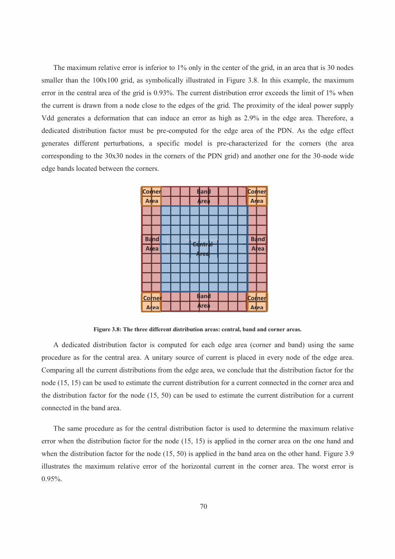
70
The maximum relative error is inferior to 1% only in the center of the grid, in an area that is 30 nodes
smaller than the 100x100 grid, as symbolically illustrated in Figure 3.8. In this example, the maximum
error in the central area of the grid is 0.93%. The current distribution error exceeds the limit of 1% when
the current is drawn from a node close to the edges of the grid. The proximity of the ideal power supply
Vdd generates a deformation that can induce an error as high as 2.9% in the edge area. Therefore, a
dedicated distribution factor must be pre-computed for the edge area of the PDN. As the edge effect
generates different perturbations, a specific model is pre-characterized for the corners (the area
corresponding to the 30x30 nodes in the corners of the PDN grid) and another one for the 30-node wide
edge bands located between the corners.
Figure 3.8: The three different distribution areas: central, band and corner areas.
A dedicated distribution factor is computed for each edge area (corner and band) using the same
procedure as for the central area. A unitary source of current is placed in every node of the edge area.
Comparing all the current distributions from the edge area, we conclude that the distribution factor for the
node (15, 15) can be used to estimate the current distribution for a current connected in the corner area and
the distribution factor for the node (15, 50) can be used to estimate the current distribution for a current
connected in the band area.
The same procedure as for the central distribution factor is used to determine the maximum relative
error when the distribution factor for the node (15, 15) is applied in the corner area on the one hand and
when the distribution factor for the node (15, 50) is applied in the band area on the other hand. Figure 3.9
illustrates the maximum relative error of the horizontal current in the corner area. The worst error is
0.95%.
Central
Area
Band
Area
Corner
Area
Corner
Area
Corner
Area
Corner
Area
Band
Area
Band
Area
Band
Area

71
Figure 3.9: Maximum relative error between the current distributions simulated with SPICE and computed with the
corner distribution factor (horizontal resistors)
Figure 3.10 illustrates the maximum relative error of the horizontal current in the band area. The worst
maximal error is inferior to 0.77%.
Figure 3.10: Maximum relative error between the current distributions simulated with SPICE and computed with the
band distribution factor (horizontal resistors)
In brief, using the appropriate distribution factor for each of the three distribution areas, it is possible
to guarantee an error in the propagation of a current draw that is inferior to 1%. Figure 3.11 and Figure
3.12 show the dedicated distribution factor in the horizontal resistors for the corner area and the band area.
The dissymmetry in the distribution factor is noticeable in comparison with the central distribution factor.
In order to reduce the simulation time, a current window must be determined for the dedicated distribution

72
factor of the corner and the band areas. The same procedure as for the central area is used to determine the
current window.
Figure 3.11: Horizontal dispersion factor in the corner area
Figure 3.12: Horizontal dispersion factor in the band area
3.1.2.3 Influence of the neighboring blocks
The current draw distribution in the PDN grid also depends on the effective power supply at the
extreme nodes of the grid border. During the pre-characterization of the dispersion factor, a grid
corresponding to the whole chip is used and consequently the power supply of the grid border is the
nominal supply voltage. Unfortunately, it is not possible to simulate the whole chip due to prohibitive
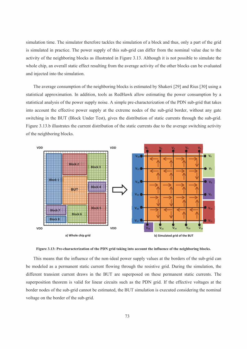
73
simulation time. The simulator therefore tackles the simulation of a block and thus, only a part of the grid
is simulated in practice. The power supply of this sub-grid can differ from the nominal value due to the
activity of the neighboring blocks as illustrated in Figure 3.13. Although it is not possible to simulate the
whole chip, an overall static effect resulting from the average activity of the other blocks can be evaluated
and injected into the simulation.
The average consumption of the neighboring blocks is estimated by Shakeri [29] and Rius [30] using a
statistical approximation. In addition, tools as RedHawk allow estimating the power consumption by a
statistical analysis of the power supply noise. A simple pre-characterization of the PDN sub-grid that takes
into account the effective power supply at the extreme nodes of the sub-grid border, without any gate
switching in the BUT (Block Under Test), gives the distribution of static currents through the sub-grid.
Figure 3.13.b illustrates the current distribution of the static currents due to the average switching activity
of the neighboring blocks.
Figure 3.13: Pre-characterization of the PDN grid taking into account the influence of the neighboring blocks.
This means that the influence of the non-ideal power supply values at the borders of the sub-grid can
be modeled as a permanent static current flowing through the resistive grid. During the simulation, the
different transient current draws in the BUT are superposed on these permanent static currents. The
superposition theorem is valid for linear circuits such as the PDN grid. If the effective voltages at the
border nodes of the sub-grid cannot be estimated, the BUT simulation is executed considering the nominal
voltage on the border of the sub-grid.
BUT
Block 1
Block 2 Block 3
Block 6
Block 8
Block 4
Block 7 Block 5
V1 V2 V3
V6
V5 V4
V16 V15 V14 V12 V13
V7
V8
V9
V10
V11
V17
V18
V19
V18
V17
V18
VDD VDD
VDD VDD
a) Whole chip grid b) Simulated grid of the BUT
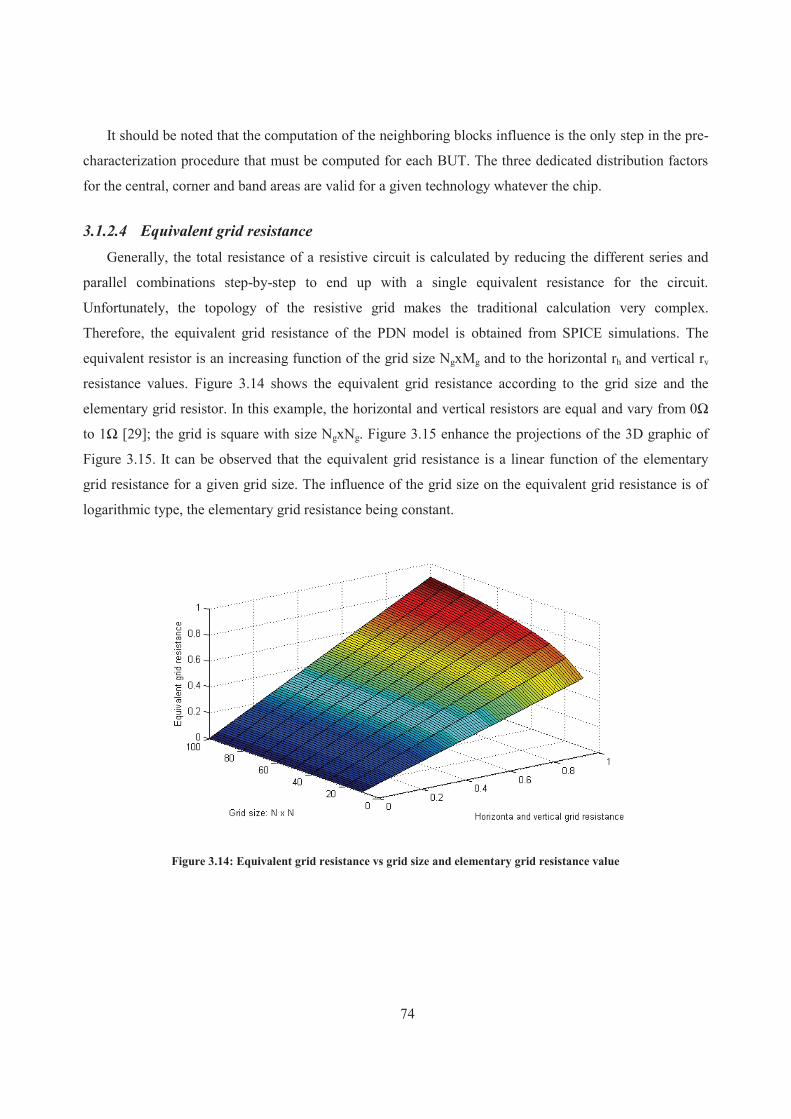
74
It should be noted that the computation of the neighboring blocks influence is the only step in the pre-
characterization procedure that must be computed for each BUT. The three dedicated distribution factors
for the central, corner and band areas are valid for a given technology whatever the chip.
3.1.2.4 Equivalent grid resistance
Generally, the total resistance of a resistive circuit is calculated by reducing the different series and
parallel combinations step-by-step to end up with a single equivalent resistance for the circuit.
Unfortunately, the topology of the resistive grid makes the traditional calculation very complex.
Therefore, the equivalent grid resistance of the PDN model is obtained from SPICE simulations. The
equivalent resistor is an increasing function of the grid size NgxMg and to the horizontal rh and vertical rv
resistance values. Figure 3.14 shows the equivalent grid resistance according to the grid size and the
elementary grid resistor. In this example, the horizontal and vertical resistors are equal and vary from 0Ω
to 1Ω [29]; the grid is square with size NgxNg. Figure 3.15 enhance the projections of the 3D graphic of
Figure 3.15. It can be observed that the equivalent grid resistance is a linear function of the elementary
grid resistance for a given grid size. The influence of the grid size on the equivalent grid resistance is of
logarithmic type, the elementary grid resistance being constant.
Figure 3.14: Equivalent grid resistance vs grid size and elementary grid resistance value

75
Figure 3.15: Equivalent grid resistance vs elementary grid resistance (left) and equivalent grid resistance vs grid size
(right)
For the equivalent grid resistance, it can be considered that the equivalent resistance will always be
lower than 1Ω for a 100x100 grid. The equivalent grid resistance is used in section 2.5 to determine the
self-IR-Drop.
3.2 Electrical model for the current distribution in a resistive and capacitive
grid
The previous section tackles the problem of IR-Drop taking into account only the parasitic resistive
elements of the PDN. Consequently, in this first approach a resistive grid is suggested to model the PDN.
The IR-Drop phenomenon is caused by the currents that flow through the PDN and generate supply
voltage drop due to the parasitic resistances. Although the resistive grid makes it possible to simulate the
distribution of IR-Drop through the IC, the current distribution is also affected by other parasitic elements
present in the PDN. Therefore parasitic inductive and capacitive elements must also be considered in the
PDN electrical model.
It is important to note that our work deals with delay fault simulation of logic circuits in the context of
IR-drop induced delay and thus, it is necessary to estimate the drop caused by the parasitic resistances.
This section is an extension of our work that analyses the presence of other parasitic elements.
The inductance of the on-chip PDN has traditionally been disregarded because the network inductance
is dominated by the parasitic inductance of the package pins and bonding wires and pads. Inductive
elements are omitted and only the presence of capacitive parasitic elements in the PDN is analyzed. This

76
section focuses on the study of the different parasitic capacitive elements and their impact on the current
distribution. Finally, a PDN resistive and capacitive model is suggested, which includes the most relevant
capacitive elements of the PDN.
3.2.1 Different types of capacitive elements
The first step is to analyze all the types of capacitive elements that could have an impact on the
current distribution behavior. Capacitive elements can be parasitic capacitors (due to the physical
superposition of electrical elements) or capacitors that are intentionally included during the design
process:
· Parasitic capacitors of the physical PDN. Parallel conductive wires of the PDN behave as
capacitive elements. The conventional way to model this parasitic capacitive element is to
include small capacitors regularly in the PDN resistive model. The size of these capacitors is
determined by the layout parameters of the PDN. These capacitors are connected to every
node of the resistive grid. An electrical analysis of the parasitic capacitors of the grid is
described in detail in section 3.2.4.1.
· Intentional decoupling capacitors. In the design phase, on-chip decoupling capacitors are
deliberately included in the PDN. Decoupling capacitors are an efficient way to reduce the
power supply noise created by the transient elements in the IC. Moreover, placing some
decoupling capacitors in the design reduces power supply fluctuations between different areas
of the IC. Consequently, decoupling capacitors reduce the IR-Drop impact.
Intentional decoupling capacitors are much larger than the parasitic capacitive elements of the
PDN and their placement is determined during the PDN design phase using commercial tools
(such as RedHawk, PrimeRail and HyperLynx). Therefore, value and placement of the
decoupling capacitors are known. Section 3.2.4.2 illustrates an electrical model for intentional
decoupling capacitors.
· Intrinsic decoupling capacitors due to non-switching gates. The CMOS transistors of the
logic gates have intrinsic decoupling capacitance elements due to their internal electrical
parameters and the interconnection capacitance [47]. The equivalent decoupling capacitor of a
gate is a function of the internal transistor capacitance and the interconnection capacitance. It
can be calculated using the layout information. In a single gate, the intrinsic decoupling
capacitor is negligible, but it becomes very significant when a large number of non-switching

77
gates are connected to the same node of the PDN. Section 3.2.4.3 shows an electrical model
that includes the intrinsic decoupling capacitors due to non-switching gates.
3.2.2 Analysis of the capacitive elements
The second step is to study the impact of the above listed capacitive elements on the current
distribution through the PDN. Computing the current distribution in a resistive grid is easier than in a
resistive-capacitive (RC) grid because in the first case the calculation involves only a system of linear
equations. In addition, this system of equations does not include integrals or derivatives. For this reason, a
predefined distribution factor can be used to predict the current distribution in the resistive grid. The
mathematical analysis of the current distribution through a resistive and capacitive grid involves integrals
and derivatives, making it more complicated to predict the current distribution. In addition, the RC grid
includes several capacitive elements with different values and each one is placed in a given node of the
PDN. Thus, simplifying the electrical schematic using the traditional calculation of equivalent impedance
is extremely difficult as the mathematical analysis involves solving a system of differential equations. In
brief, a simple system of differential equations could be solved, but in this case it is unfeasible due to the
topology complexity and the huge number of variables.
In order to evaluate the impact of the capacitive elements on the current distribution, didactic
examples are simulated using SPICE. These simple examples allow us to apprehend the behavior of the
complex set of capacitive elements. For the sake of clarity, a RC model with a limited number of
capacitors is used to make easier the analysis of the capacitors contribution to the distribution factor. For
the same purpose, instead of a two-dimensional grid, a resistive and capacitive one dimensional linear
PDN is used.
3.2.2.1 Example 1: Resistive PDN with a single capacitor
In the first simulation, the current distribution through a resistive line on the one hand and through a
resistive and capacitive line on the other hand are compared in the case of a current draw generated by a
switching gate. The first schematic includes two resistors R1 and R2 as shown in Figure 3.16.a. On the
right side of the schematic, at the terminal of the line that is opposite Vdd, an inverter gate is connected to
the resistive line at node n1. For the second schematic, the electrical structure is the same except that a
capacitor C1 is included between R1 and R2 as illustrated in Figure 3.16.b. In both simulations, the inverter
input switches from 0 to 1. Therefore, a current flowing from Vdd to the inverter appears across the
different elements of the PDN line.

78
Figure 3.16: Simulation of the resistive PDN with a single capacitor
In the first simulation with only resistive elements, the current across R1 and R2 is identical to the
current draw Idraw because Vdd is the only source that can provide current. Figure 3.17 shows the current
across R1 and R2 and the voltage in nodes n1 and n2 for the purely resistive simulation. As expected, the
voltage drop in node n1 is more pronounced than in node n2 but in both nodes the voltage returns to the
nominal voltage (Vdd) when the current draw finishes.
Figure 3.17: Currents and voltages in the simplified resistive PDN model
On the other hand, Figure 3.18 shows the results provided by SPICE for the second simulation. In this
case, although the current across R1 is equal to the current draw, the current in R2 is shifted in time and its
maximum peak is smaller with respect to the current draw. Vdd is no longer the only source able to
provide current. Current variation across R2 is due to the discharging and charging currents of the
capacitor C1.
VDD
0 1
Cload
Inv
R2 R1 n2 n1
VDD
0 1 C1
Cload
Inv
R2 R1 n1 n2
a) Resistive PDN b) Resistive PDN with a single capacitor
Idraw Idraw
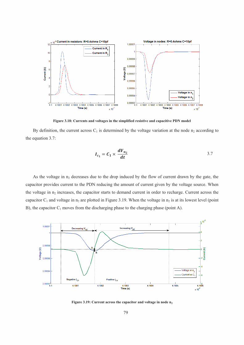
79
Figure 3.18: Currents and voltages in the simplified resistive and capacitive PDN model
By definition, the current across C1 is determined by the voltage variation at the node n2 according to
the equation 3.7:
3.7
As the voltage in n2 decreases due to the drop induced by the flow of current drawn by the gate, the
capacitor provides current to the PDN reducing the amount of current given by the voltage source. When
the voltage in n2 increases, the capacitor starts to demand current in order to recharge. Current across the
capacitor C1 and voltage in n2 are plotted in Figure 3.19. When the voltage in n2 is at its lowest level (point
B), the capacitor C1 moves from the discharging phase to the charging phase (point A).
Figure 3.19: Current across the capacitor and voltage in node n2

80
Regarding now the relation between the current provided by the capacitor and the current draw, all the
voltages and the currents of the simulation are plotted in Figure 3.20. Note that the current across the
resistor R1 is equal to the current draw of the inverter. We can observe that the current demanded by the
inverter IR1 is at its maximum at time t1. However, the current provided by the voltage source, IR2 in Figure
3.20, is at its maximum later, at time t3. It is because the capacitor provides a part of the demanded
current. The maximum of the current IR2 is correlated with the minimum voltage in the node n2 and the
capacitor transition between the charging and discharging phases. In brief, the transition between the
discharging phase and the recharging phase cannot be associated to the current draw peak. Regarding the
voltage in the node n1, we can observe that the minimum voltage in the node n1, at time t2, is not correlated
with the current draw peak, at time t1. Indeed, the voltage in the node n1 depends on the voltage drop in R1
and in R2. For the first simulation with a purely resistive PDN, currents across R1 and R2 are equal to the
current draw. Consequently, voltage in the node n1 is proportional to the current draw and thus, the
maximum current draw and the minimum voltage in node n1 are at the same time. For the second
example, the current across the resistor R1 is equal to the current draw but the current across R2 is
different. Consequently, voltage is node n1 is not correlated with the current draw. We can conclude that
all the currents and voltages are affected by the capacitor with the exception obviously of the current draw
of the invertor.
Figure 3.20: Current across each element and voltage in each node

81
VDD
0 1 0C1
Cload
Inv
R2 R1 n1 n2
VDD
0 1 C1
Cload
Inv
R2 R1 n1 n2
a) Phase 1:
Current draw active
Discharging capacitor
ΔVn2 < 0
IC1 < 0
IR1= IR2 + |IC1|
b) Phase 2:
Current draw active
Charging capacitor
ΔVn2 > 0
IC1 > 0
IR2= IR1 + IC1
VDD
1 C1
Cload
Inv
R2 R1 n1 n2
c) Phase 3:
Charging capacitor
ΔVn2 > 0
IC1 > 0
IR2= IC1
IR2
|IC1|
Idraw
Idraw
IC1
IC1
IR1= IR2+ |IC1|
IR1
IR2
IR2= IR1+ IC1
IR1= 0 Idraw= 0
Figure 3.21: Capacitor discharge and charge phases.
In summary, we can define different transition phases as illustrated in Figure 3.21:
· Phase 1: The gate switches and starts to demand current. The voltage in n2 decreases and the
capacitor starts to discharge. The capacitor provides part of the required current and the
voltage source provides the rest (IR1 = IR2 + |IC1|).
· Phase 2: The current draw of the gate starts to decrease and voltage in n2 begins to rise. The
capacitor starts to demand current, which is provided by the voltage source. At this moment,
the current draw of the gate and the current required by the capacitor are active and the
voltage source must supply both currents (IR2 = IR1 + IC1).

82
· Phase 3: When the current draw no longer demands current, there is a small period during
which the capacitor finishes to recharge. This means that the voltage source must furnish
some current only due to the capacitor effect (IR2 = IC1).
3.2.2.2 Example 2: Resistive PDN with several capacitors
In the real PDN grid, parasitic capacitive elements may be multiple and may be present in every node
of the grid. Although the previous example already analyzed the current distribution with a single
capacitor connected to the PDN, it is also important to analyze the impact of several capacitors on the
current distribution. For this reason, a new schematic as shown in Figure 3.22 including several capacitors
in the PDN line is simulated with SPICE.
Figure 3.22: Simplified resistive and capacitive PDN with five capacitors
Observing in Figure 3.23 the waveforms provided by SPICE, we conclude that the voltage drop in the
nodes gets obviously smaller when the nodes are further from the current draw. In addition, currents
provided by a capacitor quickly decrease when the distance between the capacitor and the node where the
inverter is connected increases.
VDD
0
1 C1
Cload
R2 R1 n1 n2 R3 R4 R5 R6 n3 n4 n5 n6
C2 C3 C4 C5
Idraw
Ic1 Ic2 Ic3 Ic4 Ic5

83
Figure 3.23: Simulation current and voltage waveforms for a multi-capacitor PDN.
In a simulation without capacitors, the current provided by the voltage source is equal to the current
drawn by the switching gate. In the present case, the maximum of current provided by the voltage source
decreases because the current contribution of all the capacitors fulfills part of the current draw as
illustrated in Figure 3.24. However, it must provide current over a longer period of time in order to
recharge the capacitors.

84
Figure 3.24: Current draw vs current provided by the voltage source with/without capacitive elements
When the voltage drop generated by the current draw, illustrated in Figure 3.23.c, starts to decrease,
the capacitors that have discharged must be recharged. Capacitors that are closer to the switching gate
require more current to recharge than the further ones because they have provided more current during the
discharging phase (phase 1). Consequently, the voltage source must provide the necessary current to
recharge the capacitors and concurrently satisfy the current draw, which is still active (phase 2).
Moreover, the current demand to recharge the capacitors lasts over time. In other words, the capacitors
start to demand current at different times with respect to each other: starting from the gate, the closest
capacitor starts to recharge just before its left neighbor and so and so forth for the rest of the capacitors. In
this way, the farthest capacitors keep supplying current and supporting the voltage source with their
current contribution for a while. Gradually, these capacitors start to demand current themselves and stop
supporting the voltage source. As already commented in the first example, the recharging phase continues
even after the current draw has finished (phase 3). When the last capacitor enters into the recharging
phase, the current draw has already finished and most of the capacitors are already recharged.
The amount of current demanded by a capacitor to the source for its recharge is the same as the
current it provided to the current draw. Therefore, the voltage supply must provide in the end the entire
current draw, however the capacitors discharging and charging process changes the timing. In other
words, the voltage supply provides the same amount of current but over a longer period of time. This
means that the area of the region bounded by the Idraw curve on the top and the x-axis on the bottom must
be equal to the area of the region bounded by the IVsource curve on the top and the x-axis on the bottom as

85
illustrated in Figure 3.25. Moreover, this equivalence is also true for the current across each resistor of the
PDN line because capacitors give and receive the same amount of current.
Figure 3.25: Signed area of the regions in the xy-plane bounded by Idraw and IVsource
Currents flowing across the resistors are impacted by the presence of capacitors. The further away
from the current draw they are, the smaller the magnitude of the current across the resistors and the longer
this current is active. Compared to the PDN model without capacitive elements, the voltage drop in a node
of the line generated by the current draw is consequently smaller in magnitude but longer in time.
In brief, the voltage source is responsible for providing the whole current requested by the gate current
draw. When the current starts to flow through the PDN, the capacitive elements connected to the PDN
start to provide some current. Capacitors close to the gate are more sensitive to the current demand and
their discharging rate is greater than the more distant ones. While the required current increases,
capacitances provide current; when the required current decreases these capacitances no longer provide
current but absorb it. They complete this process in an orderly manner: the first ones are the capacitors
that are close to the gate; the latter ones are more distant capacitors on the Vdd line.
3.2.2.3 Impact of capacitive elements on the current distribution
In conclusion, the presence of capacitances in the PDN model modifies the current distribution in
magnitude and time:
· The amount of current released by each capacitor increases when the capacitor value
increases.

86
· The amount of current released by each capacitor is a decreasing function of its distance to the
switching gate.
· The time during which a capacitor provides current increases with its distance to the switching
gate.
· The time after which a capacitor is completely recharged is an increasing function of its
distance to the switching gate.
· The active current distribution lasts longer than the duration of the current draw itself.
· The impact of the capacitive elements on the current distribution decreases when their
distance to the gate increases.
The further away from the switching gate they are, the smaller the amount of current first provided
and then demanded by the capacitor. This means that the impact of the capacitors may be negligible across
greater distances. These conclusions make it possible to suggest a model that includes only the capacitive
elements within a capacitance window around the switching gate.
3.2.3 Theoretical analysis and simplified model
Although SPICE simulations provide a descriptive idea of the impact of capacitive elements, a
mathematical analysis of the capacitances impact is necessary to understand the current contribution of the
capacitive elements in function of the electrical parameters of the PDN. In order to have a more precise
understanding of the current distribution variations due to the capacitive elements, a simple schematic is
suggested in Figure 3.26. In this schematic, the PDN model has been simplified to one dimension. RgL and
RgR represent the equivalent resistance of the PDN in the left and right branch respectively and Rg is the
grid resistor connected to both branches. For the sake of simplicity, the capacitive elements were modeled
as a simple capacitor in the previous SPICE examples. However the intrinsic decoupling capacitors due to
non-switching gates must be model as a resistor and a capacitor in series as we will see in the next section.
For this reason, in this schematic the capacitive element is modeled as a resistor Rs and a capacitor Cs
connected in series. This capacitive element is connected to the node n1. Finally, the current draw of the
switching gate is modeled as a current source I(t) and is connected to the node n2.

87
VDD
Cs
RgL Rg n1 n2
VDD
RgR
Rs IL IR IR
Ics RIg
Ics
I
nc
Figure 3.26: Generic schematic for the mathematical analysis
As explained in the previous section, the current across the capacitor is active even when the
switching gate does not demand current any longer. Therefore, the mathematical solution of the electrical
circuit must be tackled in two phases: when the current draw is active and when the current draw has
finished.
3.2.3.1 Phase 1: current draw active
Given I(t) the current draw, the relation between the currents can be determined using Kirchhoff's
circuit laws:
3.8
3.9
Applying the nodal analysis between the two nodes connected to Vdd, we deduce the equation 3.10:
3.10
By definition, the current across CS is determined by the voltage variation at the node nc according to
the equation 3.15:
3.11

88
Therefore, is defined by a first-order linear differential equation:
3.12
Considering that the capacitor is charged at t0=0, the initial condition is:
3.13
Therefore, is a function of all the resistive elements of the power grid and it also depends on the
capacitive elements and the current draw. The current draw of all the different gates is known and
described as an array of values in the pre-characterization library, but a function approximation is required
to solve the equation. In this case, a parabolic function approximation is used.
3.14
The current drawn from Vdd by a switching inverter and the corresponding approximated parabolic
function are plotted in Figure 3.27. Although the current draw is not exactly a parabola, the approximation
makes it possible to simplify the differential equation resolution with an acceptable accuracy.

89
Figure 3.27: Parabolic function approximation for the current draw
Once all the electrical elements are known, the differential equation can be solved. The general
solution to a linear equation can be written as , where is the solution to the
associated homogeneous differential equation and is a particular solution. The associated
homogeneous differential equation of the equation 3.12 is:
3.15
The solution of the associated homogeneous differential equation is an exponential function:
3.16
where the time constant τ is:
3.17
The time constant depends on the capacitor value and also on all the resistive elements of the
schematic. At the same time, the charging and discharging curve of the capacitor depends on the time

90
constant. Therefore, we conclude that the charging and discharging curve of the capacitor depends on the
resistive elements of the PDN.
To find a particular solution, the following solution is used:
3.18
where the constants A, B and D of the particular solution are computed applying the initial condition to
the differential equation 3.13. Once the particular solution has been computed, the general solution of the
differential equation is described in the following equations:
3.19
3.20
3.21
3.22
3.23

91
3.2.3.2 Phase 2: current draw non-active
To solve the differential equation once the current draw is finished, the functions are defined using the
same convention as in the previous section, but including the notation prime. When the current draw is
inactive, the differential equation deduced in the previous section is correct except that I(t) is 0.
Consequently is defined by the homogenous differential equation 3.24:
3.24
To maintain the continuity in the function, the voltage in the node connected to Rs and Cs must be
the same when the current draw finishes at t= -a/b.
3.25
Once the initial condition is defined, the differential equation can be solved. The general solution for
the homogenous differential equation 3.24 has the following form:
3.26
where τ’ is the time constant. Applying the initial condition, we deduce the general solution of the
differential equation.
3.27
3.28

92
3.29
3.30
3.2.3.3 Complete theoretical analysis
Therefore, the electrical behavior of a capacitive element composed of Rs and Cs can be determined by
solving the differential equation and applying a parabolic function approximation for the current draw.
The current across Cs calculated mathematically and obtained from SPICE are compared. Figure 3.28
shows the waveform simulated with SPICE and the waveform computed using the differential
equation. The computed waveform is very satisfactory given that the current draw is approximated as a
parabolic function.
Figure 3.28: Simulated and computed current across the capacitor CS
The simplified schematic helps to understand the impact of capacitive elements on the current
distribution. As described in section 3.2.2.3, the current across the capacitive elements depends on the
capacitor value and also on all the resistive elements of the PDN model. The current provided by the

93
voltage source lasts longer than the current draw due to the recharging process of the capacitive elements.
Finally, theoretical analysis confirms that the maximum current peaks are displaced in function of the time
constant.
For a schematic with several capacitors, the mathematical analysis requires to solve a system of
differential equations. Given the complexity of the resolution and the number of possible combinations for
the capacitive elements, mathematical solution for several capacitors is extremely complex. Fortunately,
the didactic SPICE simulation and the resolution of the simplified model have shown that a capacitor
connected far from the current draw provides a very small current in comparison to the current draw
amplitude. This means that it is not necessary to take into account all the grid capacitors. Only
neighboring capacitors have a real impact on the current distribution. We remember that a current window
was defined for the resistive grid. A capacitance window can also be defined to determine the area where
the current distribution is affected by the capacitive elements. Furthermore, the current across a capacitor
depends directly on the capacitance value. Therefore, the capacitance window depends on the resistive
elements of the grid and also on the size of the capacitors. The analysis and definition of the capacitance
window is presented in Chapter 4.
3.2.4 Electrical model for capacitive elements
As commented in section 3.2.1, there are different types of capacitive elements in the PDN. Their
characteristics and locations are different and, for this reason, different electrical models are required. In
this section, an electrical model for every type of capacitive element is proposed.
3.2.4.1 Model for the PDN parasitic capacitors
The conventional model for the capacitive elements of the PDN includes capacitors connected to
every node of the PDN. The capacitor size, which depends on the capacitance density (layout parameters)
of the PDN, is known. Therefore, the traditional resistive grid must include small capacitors connected to
every node of the grid. As these capacitors are very small, the first hypothesis is that the contribution of
the grid capacitors to the current distribution through the PDN will be limited.
In order to determine the impact of the grid capacitors, SPICE is used to compare the current
distribution through a resistive grid with parasitic capacitors in every node on the one hand and through a
purely resistive grid on the other hand. The current across the resistive elements of the power grid in both
cases is observed. In addition, the average normalized root mean square deviation of the currents across all
the resistors of the grid is computed. In Figure 3.29, the average NRMSD is plotted for different grid
resistor values (from 0.01 to 1Ω) and grid capacitor values (from 0pF to 1pF) [13].

94
Figure 3.29: Average NRMSD of PDN currents with and without grid capacitors
For the distribution factor, defined in chapter 3, a current window has been described and the fractions
of the current draw smaller than 1% were disregarded. The same convention is used for the average
NRMSD: if the average NRMSD is smaller than 1%, the parasitic capacitors of the physical PDN are
omitted. The contour function shown below makes it possible to determine if the capacitive effect of the
grid is negligible in function of the grid resistor and grid capacitor values (respectively Rg and Cg). Grid
capacitors Cg whose combination with Rg suppose an average deviation smaller than 1% are omitted from
the electrical PDN model. In brief, the parasitic capacitors of the physical PDN can be disregarded in most
cases.
Figure 3.30: NRMSD contour for PDN currents with and without grid capacitors

95
3.2.4.2 Model for decoupling capacitors
Decoupling capacitors are real physical capacitors connected to the PDN. The decoupling capacitor
value is significant in comparison with the grid capacitor value and must be taken into account in the
current distribution as the decoupling capacitors reduce the voltage drop propagation through the PDN.
The decoupling capacitors are not connected to all of the PDN nodes, their placement is determined during
the PDN design phase using commercial tools (such as RedHawk, PrimeRail and HyperLynx). As their
values are known, the decoupling capacitors are modeled as a single capacitor Cd connected to the
corresponding nodes.
3.2.4.3 Model for intrinsic decoupling capacitors due to non-switching gates
The CMOS transistors of the logic gates contain a number of internal parasitic capacitances.
Therefore, every logic gate connected to the Vdd PDN and the Gnd PDN behaves as a small decoupling
capacitor. These intrinsic decoupling capacitors depend on the transistor electrical parameters. Therefore,
their value can be calculated using the layout information. Note that interconnection capacitances may
also be considered as illustrated in Figure 3.31.
Figure 3.31: Gates input capacitances and interconnection capacitance connected to a node
The intrinsic decoupling capacitor of a single logic gate is negligible. However the high number of
logic gates connected to the same node makes this capacitive impact quite significant. Indeed they will
produce a determinant impact on the current behavior. Note that these intrinsic decoupling capacitors are
not connected directly to the PDN nodes but through conducting N or P transistors, which are modeled as
a single resistance Rs in the ‘on’ transistor side. The transistor resistance impedes the contribution of
current from the logic gate to the PDN preventing the current from being harmful to the IC integrity.
In brief, the non-switching gates connected to the PDN are modeled as a resistor Rs and a capacitor Cs
in series. The resistor value Rs is the on transistor resistance and the capacitor value Cs is the output
capacitance Cout of the gate. Rs and CS depend on the type of gate and on the input vector. Figure 3.32
illustrates the complete electrical model for a non-switching gate.

96
Cout
Vdd grid
Gnd grid
on
off Cs = Cout
Rs = Ron_PMOS
Vdd grid
Gnd grid
Rs = Ron_NMOS
Cs = Cout
Cout
Vdd grid
Gnd grid
on
off
a) PMOS transistor on b) NMOS transistor on
1 0
Figure 3.32: Electrical model for the non-switching gates
For all the non-switching gates connected to the power grid, the resistor Rs and capacitor Cs are
connected to the PDN in parallel. The question now is how to approximate a single resistor Req and
capacitor Ceq connected to the grid in order to get an equivalent to the whole bench of resistances Rs and
capacitances Cs. For identical non-switching gates, the equivalent resistor Req and capacitor Ceq are
defined by:
3.31
3.32
Assuming now different types of gates connected to the same node, it is necessary to make an
approximation because the mathematical computation is extremely complex. In this context, we have
considered that all the gates have the same Rs and Cs values for the sake of simplicity. Future works can be
dedicated to find a more accurate model.

97
4 Simulator implementation
In chapter 1, the IR-Drop phenomenon has been introduced in the view of implementing an IR-Drop
simulator that allows the prediction of the induced delay at the block level. IR-Drop depends on all the
currents generated by the logic gate switchings of the IC and also on the resistive elements of the PDN,
and consequently on the distribution of the currents through the PDN. In Chapter 2, an electrical model at
the gate level has been developed and the pre-characterization procedure to generate the gate library has
been explained in detail. The pre-characterized gate library contains the electrical models for the gate
delay, the dynamic currents and the static currents in function of the voltage drop of the PDN.
Furthermore, the electrical model for the PDN and the current distribution through it have been studied in
Chapter 3. Consequently, once defined an electrical model at the gate level and an electrical model for the
PDN, the voltage drop in every point of the PDN can be computed and we can estimate the induced delay
due to the IR-Drop phenomenon.
By definition, IR-Drop concerns the resistive elements of the PDN and the dynamics currents
generated when a gate switches and thus, both elements are determinant in the induced delay estimation.
Regarding the results of Chapter 2, dynamic currents are predominant in comparison with static currents.
In the same way, current distribution through the PDN is highly dependent on the resistive elements of the
PDN. For this reason, an implementation of the simulator is developed including the dynamic currents and
computing the voltage drops using a resistive grid. In the first sub-section of this chapter, the
implementation details and the validation results are presented.
On the other hand, including the static currents and the capacitive elements in the PDN model
improves the accuracy of the simulator because both elements generate variations in the current
distribution and thus, impacts the voltage drops. Whereas the static currents are injected in every node in
the same way as the dynamic currents, computing the current distribution in a RC grid involves some

98
problems. In the second sub-section of this chapter the problematic to develop a simulator that includes
capacitive elements in the PDN model is analyzed and a simplification method is suggested.
The software of the IR-Drop induced delay simulator (MIRID) has been developed by the department
of Informatics and Mathematics of the University Passau (GERMAY). This dedicated software employs
the electrical model developed at the LIRMM (FRANCE) in the context of a French-German
collaboration project.
4.1 Simulation principle and validation
In the implementation of the simulator a resistive PDN model is used to inject the current draws of
the gate library (defined in section 2.3). Regarding gate static currents (section 2.3.3), the static current
contribution is negligible as far as the number of gates connected to the same node is small. It means the
static currents must be evaluated only when a high number of gates is connected to the same node. In the
other case, these currents can be omitted reducing the simulation computation time. Note that
consideration of static current in further version will be straight forward knowing that the gate library
contains electrical models for the static and dynamic currents.
4.1.1 Simulator algorithm
Knowing, from the pre-characterization phase, the gate electrical parameters and the horizontal and
vertical distribution factors in function of the technology, the delay of a circuit induced by the IR-Drop
phenomenon can be predicted. As explained in section 1.3, an event-driven simulation designed for a logic
simulator and an electrical simulator is performed. The logic simulation determines the logic value
propagation at the block level. When a gate switches, the voltage drop at his power and ground nodes
must be predicted to determine the gate delay and current draws. The gate delay is computed as a function
of different electrical parameters (Vswing1, Vswing2 and Cload). In the same way, the current draws are derived
in function of the electrical parameters of the gate and then injected into the PDN grid. Therefore, the
logic and electrical simulations are performed concurrently.
Consequently, the data structure of the mixed-mode simulator is composed of both the logic structure
of the simulated block and the electrical structure of the PDN (one for Vdd and one for Gnd). Figure 4.1
illustrates the mixed-mode structure. In addition, given the logic structure of the circuit under test, the
connection between each gate and the PDN grid (Vdd and Gnd) is stored in the data structure. For this
reason, the logic structure of the circuit is closely connected to the electrical structure of the resistive grid
through power and ground connections. Moreover, the logic and the electrical simulations communicate
through the input switch events and the output switch events.

99
Therefore, given an input pattern, the simulation starts by applying the input pattern to the logic
structure. At each time step (in this case, for every picosecond), the logic simulation propagates the logic
values. If a gate switches, an input switching event is generated and sent from the logic simulation to the
electrical simulation. When the input switching event arrives to the electrical simulation, the voltage drop
in the node of the switching gate and the voltage drop in the node of the upstream gate are computed. The
delay and the current draw of the switching gate are calculated using the stored gate library as a function
of the electrical parameters. The corresponding current draw of the gate is injected into the PDN model. In
this context, injection of the current into the PDN means that for every input switching event the
computed current draw of the gate is stored in the current event queue and processed later.
VDD PDN model
Logic block
d
t
Ivdd
VDD1 VDD
2
GND1 GND
2
Gi
Nvdd(m,n)
Vswing2
t
Ignd
GND PDN model
Gi-1
Nvdd(i,j)
Ngnd(i’,j’)
Ngnd(m’,n’)
Vswing1
Input switching
events
Output switching
events
Output switching
events
Input switching
events
Rh(m,s)
Figure 4.1: Mixed-mode simulator
In order to explain in detail the electrical simulation, a didactical example illustrated in Figure 4.1 is
used. The gate Gi is connected to the PDN through node Nvdd(i,j) for the power supply and node Ngnd(i’,j’)
for the ground. It is important to note that logic gates are not connected necessarily to the same node, in
terms of coordinates, of Vdd and of Gnd. The upstream gate (Gi-1) is connected to the PDN through node
Nvdd(m,n) and node Ngnd(m’,n’). When the gate Gi switches at time t an input event is generated by the

100
logic simulation and the electrical simulation is activated. The electrical simulation of the PDN grid
consists of the following stages:
If gate Gi switches at time t
1. Computes the electrical parameters
1.1. Voltage swing of upstream gate Gi-1
Vswing1 (t) = V(Nvdd(m,n),t) - V(Ngnd(m’,n’),t)
1.2. Voltage swing of gate Gi
Vswing2 (t) = V(Nvdd(i,j),t) - V(Ngnd(i’,j’),t)
2. Deduces from the gate library the delay and current draws:
2.1. δ (gate,Vswing1,Vswing2,Cload)
2.2. Ivdd (gate,Vswing1,Vswing2,Cload)
2.3. Ignd (gate,Vswing1,Vswing2,Cload)
3. Stores deduced current draws in the current event queue
4. Generates output switching event at t+δ
In step 1, the simulator computes the electrical parameters related to the upstream gate and the
switching gate. Taking Vswing1(t) as an example of the computation procedure, Vswing1(t) is the difference
between the voltage in the node Nvdd(m,n) of the power PDN and the voltage in the node Ngnd(m,n) of the
ground PDN at time t, as written in equation 4.1. In other words, Vswing1(t) is the supply voltage swing of
the gate Gi-1 at time t.
4.1
Voltages in the nodes Nvdd(m,n) and Ngnd(m’,n’) are computed taking into account all the active current
draws in the PDN. These currents are stored by the electrical simulator in the current event queue. The
electrical simulator calculates the current through each horizontal resistor placed in the same line as the Gi-
1 connection node (in the Vdd and the Gnd grids). Current computation takes into account all the active
currents and their corresponding distribution factor depending on their position in the grid. Equation 4.2
describes the current across the horizontal resistors Rh(m,s).
4.2

101
The simulator computes the voltage in the node Nvdd(m,n) and in the node Ngnd(m’,n’). The voltage is
computed, as described in equations 4.3 and 4.4, calculating the voltage drop between the border of the
grid in the same line as and the Gi-1 connection node, considering only the direct horizontal line.
4.3
4.4
The same procedure for Vswing2 (t) calculation is used to compute the voltage swing of the gate Gi
at time t (equation 4.5).
4.5
In step 2, once known the electrical parameters Vswing1, Vswing2 and the load capacitance Cload, the
corresponding gate delay and dynamic currents drawn from Vdd and Gnd are deduced from the gate
library.
d 4.6
4.7
Vdd and Gnd current draws of the gate are stored in the current event queue and the simulator generates
the output switching event with the corresponding delay d(Gi). The logic simulation stores the estimated
delay of the gate and continues the logic simulation. Output gate commutation is effective when the logic
simulation arrives to the time “t+ d(Gi)”. Following the last algorithm for every switching gate of the

102
circuit, an output pattern is obtained at the end of the simulation as well as the estimated delay associated
to the output pattern.
4.1.2 Simulation validation
A first version of MIRID is developed using the suggested algorithm. The validation aims at
determining the accuracy of the electrical model and the resulting estimated delay. It should be noted that
although the proposed electrical models at the gate level (static and dynamic currents and delays) have
already been validated in Chapter 2, a further validation through realistic circuit simulation is worth being
performed. Indeed, in Chapter 2, the electrical model at the gate level and its validation are computed for
constant voltage swings. In a realistic environment, voltage swings (Vswing1 and Vswing2) evolve in time. In
addition, the possible load capacitance is quantified. It means that only Cmin multiples are taken into
account in the pre-characterization procedure while the real input capacitance of a gate may not be a Cmin
multiple. The goal of this further validation is to quantify the impact of these limitations from the gate
library pre-characterization on the MIRID results. To estimate the accuracy of the proposed electrical
models, the validation procedure is based on the comparison between results obtained from SPICE and
results obtained from MIRID. Unfortunately, the number of gates that can be simulated with SPICE is
limited. On the one hand, a large circuit cannot be simulated using SPICE. On the other hand, only a large
circuit would generate a relevant IR-Drop level in the PDN and thus, a large variation in the delay. Due to
this limitation, the validation procedure is divided into three steps:
· Comparison between MIRID and SPICE results using an inverter chain simulation in order to
validate the electrical model of the power grid and the electrical model of the current draw.
· Comparison between MIRID and SPICE results using small benchmark circuits in order to
validate the electrical model of the power grid and the electrical model of the current draw
with different values of fanout.
· Comparison between MIRID and SPICE results using a circuit dedicated to maximizing the
delay in order to validate the electrical model of the gate delay.
Note that a 100x100 grid for the PDN is used in the simulations with SPICE and MIRID. The values
of the horizontal and vertical resistances are 0.4Ω [29].

103
4.1.2.1 Validation with an inverter chain
The first experiment aim is to validate the electrical models, above all the PDN electrical model. A
simple electrical schematic is simulated using SPICE and MIRID. The schematic is made of a chain of
14 inverters connected to the Vdd and Gnd grids as illustrated in Figure 4.2. A test pattern pair (0,1) is
applied to the first inverter input (connected to node (40,47) in both Vdd and Gnd grids). Note in Figure
4.2 that half of the inverters are connected to line 40 and half to line 60. More precisely, the odd inverters
making a positive transition are connected to line 40 and the even inverters making a negative transition
are connected to line 60.
40
60
100 47 47 48 49 50 51 51 52 52 53
40
60
100 47 47 48 49 50 51 51 52 52 53
VDD grid
GND grid
Figure 4.2: Schematic of 14-inverter chain validation
Therefore, inverters with the same input transition are connected to the same horizontal line. As
justified in section 2.3.2, when a gate switches a current draw appears in the Vdd supply and another
appears in the Gnd supply. Depending on the input transition of the gate, one of the two current draws is
predominant on the other. The smaller one is more complex to model and more sensitive to the power
voltage supply. The main benefit to use this simple schematic is that all inverters connected to same line
have the same input transition and thus all their predominant current draws settle in the same supply line
(in Vdd or Gnd). Hence, the IR-Drop effect is maximized. In addition, the accuracy of the current model is

104
analyzed independently for the predominant current draw and for the weak current draw. Note that the
generated voltage drop has an imperceptible impact on the delay of a 14-inverter chain (the order of
magnitude of the additional delay is 10-6
ps, which is much smaller than the MIRID time resolution); as a
consequence, the induced delay validation is not possible using this schematic. What we want to validate
at this step is the electrical models of dynamic currents and current distribution by comparing the current
and the voltage waveforms.
Figure 4.3: Validation electrical waveforms in node and resistor (40,50) for a 14-inverter chain (ps precision)
Figure 4.4: Validation electrical waveforms in node and resistor (60,50) for a 14-inverter chain (ps precision)

105
Figure 4.3 and Figure 4.4 show some results obtained from SPICE (in blue) and MIRID (in red)
simulations. The figures exhibit the voltage waveforms of the node (40, 50) in Gnd and Vdd grids versus
time as well as the currents waveforms in the resistor (40, 50) in Gnd and Vdd grids versus time. Current
and voltage waveforms resulting from SPICE and MIRID simulations are very similar in shape and
amplitude. Obviously, some small differences appear due to the electrical model approximations. The
Normalized Root Mean Square Deviation (NRMSD) is calculated to estimate the error between MIRID
and SPICE for each electrical waveform (Table 4.1).
Table 4.1: NRMSD error for voltage and current estimation for a chain of 14 inverters (in the example nodes and
resistors)
NRMSD Vvdd NRMSD Vgnd NRMSD Ivdd NRMSD Ignd
(40,50) 4.33% 7.90% 2.02% 2.56%
(60,50) 4.03% 11.25% 1.53% 3.72%
In our first validation case, the maximal error over the entire PDN grids is 11.25% for the voltage
waveforms (at Vgnd(60,50) shown in Figure 4.4) and 3.72% for the current waveforms (at Ignd(60,50)).
Both errors correspond to the weak current draw in the Gnd supply at line 60. An inferior accuracy in the
weak current draw model was expected due to the noise sensibility. It does not mean a decrease in the
accuracy of the global electrical model because weak current draw amplitude is around 10 times smaller
than the predominant current draw and the impact of this weak current in the global voltage drop is
limited. In conclusion, we consider that the current model waveforms from MIRID are adequate and
accurate (as shown in Figure 4.3 and Figure 4.4 which are the worst cases).
4.1.2.2 Validation with a benchmark circuit
Another experiment is performed mainly to validate the current draw electrical model. In this case the
ISCAS circuit c17, which contains 2INV, 3 NAND2 and 4 NAND2, is simulated. All the gates are
connected to the center of the Vdd and Gnd grids, i.e. to node (50,50) for both supply PDN. This circuit
enables us to study the impact of the load capacitance Cload. In the previous validation, the load
capacitance of all the gates is the same: the input capacitance of an inverter (Cmin). In the current case,
different load capacitances must be taken into account during the MIRID simulation. Note that, as justified
in section 2.3.2, the gate library used in MIRID considers discrete values of the load capacitance
parameter Cload, which are multiples of Cmin.
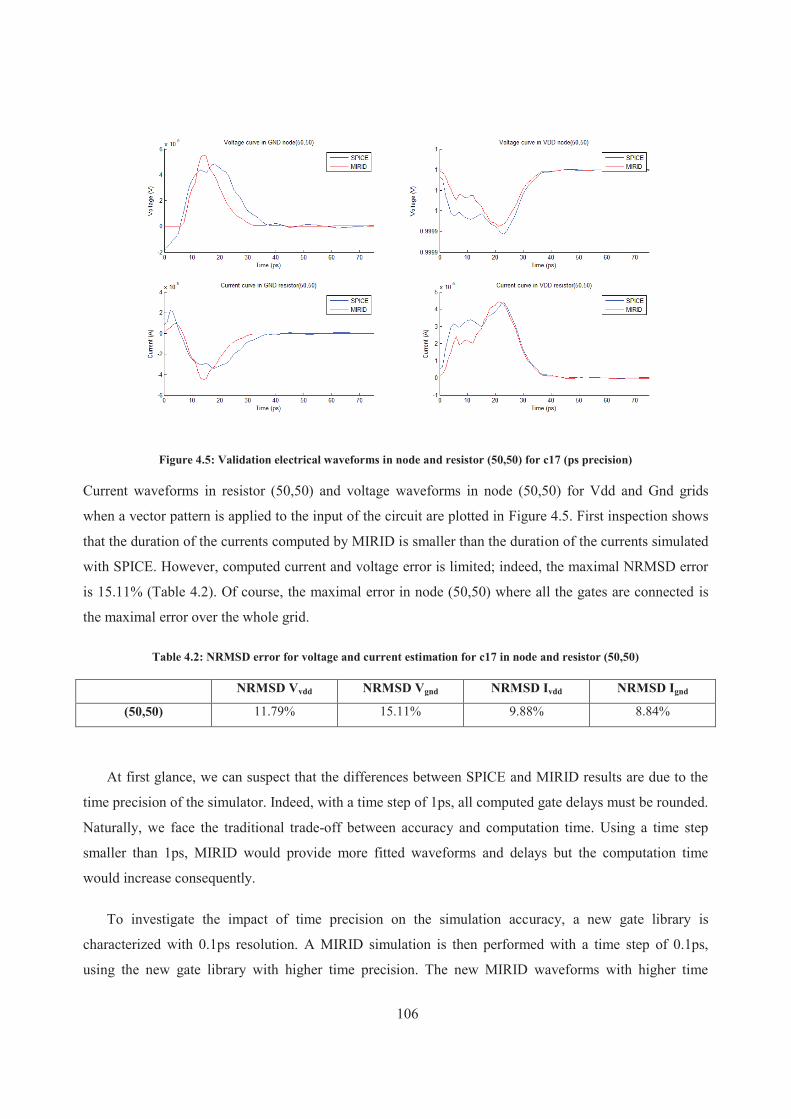
106
Figure 4.5: Validation electrical waveforms in node and resistor (50,50) for c17 (ps precision)
Current waveforms in resistor (50,50) and voltage waveforms in node (50,50) for Vdd and Gnd grids
when a vector pattern is applied to the input of the circuit are plotted in Figure 4.5. First inspection shows
that the duration of the currents computed by MIRID is smaller than the duration of the currents simulated
with SPICE. However, computed current and voltage error is limited; indeed, the maximal NRMSD error
is 15.11% (Table 4.2). Of course, the maximal error in node (50,50) where all the gates are connected is
the maximal error over the whole grid.
Table 4.2: NRMSD error for voltage and current estimation for c17 in node and resistor (50,50)
NRMSD Vvdd NRMSD Vgnd NRMSD Ivdd NRMSD Ignd
(50,50) 11.79% 15.11% 9.88% 8.84%
At first glance, we can suspect that the differences between SPICE and MIRID results are due to the
time precision of the simulator. Indeed, with a time step of 1ps, all computed gate delays must be rounded.
Naturally, we face the traditional trade-off between accuracy and computation time. Using a time step
smaller than 1ps, MIRID would provide more fitted waveforms and delays but the computation time
would increase consequently.
To investigate the impact of time precision on the simulation accuracy, a new gate library is
characterized with 0.1ps resolution. A MIRID simulation is then performed with a time step of 0.1ps,
using the new gate library with higher time precision. The new MIRID waveforms with higher time

107
precision are very similar to the waveforms with lower precision, as illustrated in Figure 4.6. The maximal
NRMSD error is 13.76% (Table 4.3). In conclusion, an increase of time precision does not improve
significantly the electrical model.
Figure 4.6: Validation electrical waveforms in node and resistor (50,50) for c17 (0.1ps precision)
Table 4.3: NRMSD error for voltage and current estimation for c17 in node and resistor (50,50) (with 0.1ps precision)
NRMSD Vvdd NRMSD Vgnd NRMSD Ivdd NRMSD Ignd
(50,50) 10.31% 13.76% 7.91% 8.98%
Although the waveforms from MIRID simulation fit slightly better with SPICE waveforms when a
gate library with 0.1ps precision is used, the error is far from being cancelled, which means that time
precision is not a key point to explain the differences between SPICE and MIRID results. An important
point is likely to be the fundamental reason of these differences: in this first version of the simulator, we
have simplified and considered that the input capacitance of the different standard gates was always the
equivalent input capacitance of an inverter Cmin (which is obviously not true for the other gates – NAND4
for example), as justified in section 2.4. As a result, the computed equivalent input capacitance of a gate is
always lower than or equal to its real value. Note that we have taken into account the fanout of the gates: a
gate connected to n downstream gates is therefore loaded by n times Cmin, but as far as each downstream

108
gate input capacitance is likely to be underestimated, the total load capacitance of a gate is necessarily
lower than or equal to the real load capacitor.
Figure 4.7: Variation of the current draw for the different output capacitance values
In Figure 4.7, the current draw reference models for different load capacitance values are plotted. The
amplitude and time duration of the current draw increase with the load capacitance value. Therefore, the
simplification related to the load capacitance, which consists in setting all the gate input capacitances to
Cmin, induces a reduction in the amplitude and time duration of the injected current draws. We can
therefore conclude that the underestimation of the load capacitance is the main cause of the variation
between MIRID and SPICE waveforms. Considering the worst case over the PDN grid, reported in Table
4.2, computed NRMSD errors are lower than 15%. These results are satisfactory especially taking into
account that the error can be reduced in future versions of MIRID considering different input capacitance
values in function of the type of gate rather than approximating it to a fixed input capacitance value.
4.1.3 Validation with a circuit designed to maximize the induced delay
IR-Drop is an electrical phenomenon due to small currents flowing through the PDN. A relevant
voltage drop in the PDN appears when there are a lot of current flows in a small area. As justified, the
estimated delay validation is complex due to the trade-off between the generation of significant voltage
drop and the number of gates that can be simulated with SPICE. Large circuits generate relevant voltage
drop in the PDN and therefore relevant induced delay. Unfortunately, such large circuits cannot be
simulated with SPICE. In this sub-section a simple logic circuit that can be simulated with SPICE is

109
proposed in order to maximize the voltage drop in the PDN and, consequently, to maximize the induced
delay.
As the global current flowing through the PDN is the addition of all the individual current draws, it is
mandatory that several gates switch simultaneously to draw a significant amount of current from the PDN.
Indeed voltage drop due the IR-Drop dissipates in time, so simultaneous switching is needed. In addition,
current distribution is very located and thus, voltage drop dissipates in space in a narrow neighborhood.
Consequently, it is necessary to find a circuit with a high density of gates gathered in a small area. To
summarize, voltage drop increases when there are several gates switching at same time in a small area. In
these conditions, currents that flow through the PDN generate a significant voltage drop.
An inverter chain is a simple circuit whose inverters switch consecutively after the input pattern
commutation. The duration of the switching activity in the chain depends on the number of inverters of the
chain and thus, the chain delay increases with the number of inverters. In addition, if the inverter chain is
connected to the PDN describing a “pseudo-circle” loop on itself, the voltage drop tackles the “pseudo-
circle” area. Moreover, if several inverter chains are connected in parallel with the same input pattern
applied at the same time, the corresponding inverters of each chain will switch at the same time and thus,
switching activity increases, enhancing consequently the induced voltage drop. In brief, using inverter
chains connected in parallel throughout the PDN generates high voltage drop. The number of chains in
parallel and the number of inverters in a chain are variable parameters that enable to regulate the level of
voltage drop.

110
n(i,j) n(i,j+1) n(i,j-1)
n(i-1,j)
n(i+1,j)
input output
a : Chain of n-inverters
c : Generic inverter-chain connection d : Specific inverter-chains connection to
maximize voltage drop in n(50,50)
nvdd(i,j+1) nvdd(i,j+1)
ngnd(i,j+1) ngnd(i,j+1)
) nvdd(i+1,j)
) ngnd(i+1,j)
+1) nvdd(i+1,j)
) ngnd(i+1,j)
,j) nvdd(i,j-1)
,j) ngnd(i,j-1)
,j) nvdd(i,j-1)
) ngnd(i,j-1)
) nvdd(i-1,j)
ngnd(i-1,j)
nvdd(i-1,j)
ngnd(i-1,j)
input
b : inverter-chains in parallel
m inverter-chains
in parallel
I3 I1 In-3 In-2 I2 In-1 In I4
input Symbol for m inverter-chains
in parallel
n-inverters
n(50,50)
Figure 4.8: Dedicated circuit to enhance the IR-Drop: logic schematic and PDN connection
In this sub-section a macro-cell composed for inverter chains is suggested to maximize the induced
delay. Figure 4.8 illustrates the structure of this macro-cell. There are three variable parameters in the
macro-cell structure.
· n inverters in each chain: A large number of inverters connected allows to generate a large
induced delay due to the IR-Drop (Figure 4.8.a).
· m chains in parallel: The more chains connected in parallel, the largest voltage drops. (Figure
4.8.b).

111
· Localization of the chain connections: Disjoint/joint/overlapping placements through the
resistive grid (Figure 4.8.d).
In our example, an inverter-chain composed of 8 inverters is our basic structure (Figure 4.8.a). When
there is no voltage drop, a chain of 8 inverters switches in 35.604ps (nominal δ0_1 is 4.903ps and nominal
δ1_0 is 3.998ps). The basic inverter chain is connected to the PDN describing a diamond (Figure 4.8.c).
This position optimizes the density of gates switching in the same area of the PDN. To induce
simultaneous switching activity, m basic inverter chains are connected in parallel at the same position (m
varying from 1 to 80). Finally, 9 groups of inverter chains in parallel are placed in the PDN (Figure 4.8.d)
generating the maximum voltage drop in the central node: 1 around the central node and 1 around each
immediate neighboring node.
Figure 4.9: IR-drop delay in function of the number of inverter chains in parallel for MIRID and SPICE
Figure 4.9 shows the delay estimated from MIRID (red curve) and obtained from SPICE (blue curve)
for one of the central chains. A curve is additionally plotted: the delay obtained for one of the central
chains when the macro cell structure is directly connected to nominal supply and ground voltages (black
curve). In this case, the delay does not change in function of the number of inverter chains connected in
parallel because there is no voltage drop. As expected, the macro-cell structure enhances the voltage drop.
As a consequence, the delay of the inverter chains increases linearly with the number of chains in parallel.
Taking as a reference the delays from the SPICE simulation, the maximum relative error is 1.17%. Note
that this result is very satisfactory, especially if we take into account that the macro-cell, which aims at
enhancing the voltage drop, also accumulates errors because the same electrical model is replicated at the
same nodes. In other cases, some errors could compensate each other; this is clearly the worst case in
terms of error accumulation.

112
4.2 Problematic of the simulation implementation using a RC grid
In a resistive PDN model, the current across every resistor at time t is a simple fraction of the global
current drawn in the PDN at time t by the switching gates. It means that calculating the current distribution
involves only linear functions. Figure 4.10.a illustrates the relationship between the current draw Ivdd and
the current Ir(i,j) across a resistor of the resistive grid. Equation 4.9 determines the fraction of the current
draw Ivdd(t) that flows across a resistor of the resistive grid, where k is a constant that depends on the
position (i,j) in the grid.
Ir(i,j)(t)= df(i,j) x Ivdd(t) 4.9
In conclusion, the distribution factor df is sufficient to exactly define the current in every element of the
resistive PDN.
VDD
A ≠ A’
t = t’
Ir(i,j) (t)= df(i,j).Ivdd
(t)
a) Resistive grid b) Resistive-capacitive grid
VDD
time
I
VDD
time
I
Ivdd
Ir(i,j)
time
I
Ivdd
Ir(i,j) A ≠ A’
t ≠ t’
0 1
Cload
Inv
VDD
t
A
A’
t t t’
A
A’
Ivdd
Figure 4.10: Current distribution through the R grid vs current distribution through RC grid
Considering a resistive and capacitive PDN model, capacitive elements imply transient phenomena
and thus, calculation of the current distribution requires complex integrals and derivatives that make the
simulation much more complex. As illustrated in Figure 4.10.b, the waveform of the current across a
resistor of the RC grid is completely different from the current draw. Indeed, not only is the maximum
value A’ different from A, but the time t’ corresponding to the maximal current in the resistor is not equal
to the time t of the maximal global current.

113
In addition, the electrical model for the intrinsic decoupling capacitor of the non-switching gates
involves the connection of capacitive elements in all the nodes of the PDN. As a result, an exact
mathematical analysis would imply to solve a system of complex differential equations. Obviously, the
simulator cannot tackle such computation due to the complexity and its prohibitive computation time. For
this reason, a simplified model is proposed in this section.
4.2.1 Capacitance window
As we have defined a time window and current window in order to reduce the simulation time, we can
also consider a capacitance window, because the capacitive elements located far away from the current
draw have a very limited effect on the global current behavior. Consequently, the model takes only into
account the capacitive elements that are close to the current draw. The other capacitive elements are
omitted for the global current behavior estimation. Obviously, the size of this capacitance window
depends on the values of resistive and capacitive elements of the RC grid.
As justified in section 3.2.4, there are three different types of capacitive elements:
· the parasitic capacitors of the physical PDN Cg, which are placed in every node of the PDN;
in most cases these capacitors are negligible (see 3.2.4.1),
· the decoupling capacitors Cd whose size and placement in the grid are known by design
(section 3.2.4.2),
· the intrinsic decoupling capacitors due to non-switching gates whose electrical model (RS and
CS) depends on the number and type of static gates connected to each node (section 3.2.4.3)
and also depends on the input vector.
In brief, the capacitive elements connected to every node of the grid are different and depend on the
simulated block as well as on the input vector. Therefore, exact prediction of the capacitance window is
unfeasible due to prohibitive computation time and high number of different variables. The first objective
here is to estimate a fix window size that could be used in any case.
For our analysis, a SPICE simulation is performed using the following simplifications for the
electrical parameters:
· The horizontal and vertical grid resistors are equal and called Rg.
· For every node, the resistors and capacitors in series representing the non-switching gates are
considered equal (Rs and Cs).
· The decoupling capacitors are omitted.

114
The resulting grid is given in Figure 4.11. For the sake of simplicity, the Rg resistances are not drawn
but are implicitly represented by the branches of the grid. Applying the above simplifications, there are
only three parameters to take into account for the simulation: Rg, Rs and Cs.
Rs
Cs
Rs
Cs
Rs
Cs
Rs
Cs
Rs
Cs
Rs
Cs
Rs
Cs
Rs
Cs Rs
Cs
Rs
Cs
Rs
Cs
Rs
Cs
Rs
Cs Rs
Cs
Rs
Cs
Rs
Cs
Rs
Cs
Rs
Cs
Rs
Cs
Rs
Cs
Rs
Cs
Rs
Cs
Rs
Cs
Rs
Cs
Rs
Cs
Rg
Figure 4.11: Standard resistive grid with parasitic resistive and capacitive elements (RC grid)
In order to determine the capacitance window, an inverter is connected to the center of the resistive
grid and the current across all the capacitors in series is reported when the inverter switches. The
amplitude of the current across each capacitor is compared to the amplitude of the inverter current draw.
Following the same criterion as for the current window calculation, only the currents across the capacitors
larger than 1% of the current draw are taken into account for the electrical model. In other words, the
capacitance window includes only the capacitive elements whose contribution to the current distribution is
significant.
Simplified schematic is simulated using realistic Rg, Rs and Cs values: The Rg values commonly
applied in SPICE simulations vary from 0.4Ω to 0.7Ω [29], the Rs values are in the range from 0 to 2Ω
and the Cs values are comprised between 0 and 10pF based on the intrinsic parasitic elements of the MOS
transistors in 45nm technology. Figure 4.12 and Figure 4.13 show the radius of the capacitive window,
given in number of nodes, in function of Rs and Cs for different values of Rg.

115
Figure 4.12: Radius of the capacitance window
Figure 4.13: Detail of the radius of the capacitance window

116
Regarding the results, we can determine the following relations:
· The area of influence of the capacitive elements decreases when the elementary grid
resistance Rg increases.
· The area of influence of the capacitive elements decreases with the series resistance Rs of the
capacitive elements.
· The area of influence of the capacitive elements decreases when the series capacitance Cs of
the capacitive elements increases.
By definition, the current across the resistive-capacitive element (Rs and Cs) is proportional to the
capacitance value (Cs). A bigger capacitor can provide more current. In addition, the current across the
capacitive element is inversely proportional to the resistor value Rs. We analyze the resistance effects:
· If the resistance Rs of the non-switching gates is high, the current will flow mainly from the
power supply to the switching gate.
· If the resistance Rg of the grid is high, the current will flow predominantly from the capacitor
Cs to the switching gate.
In any case, it clearly appears in Figure 4.12 that a window of 5 to 6 nodes around the switching gate
may be of interest whatever the values of Rs, Rg and Cs.
If we consider the case of decoupling capacitors that are added by design, these capacitors are not
connected to every node of the grid. Therefore, simulating a resistive and capacitive grid with large Cs in
every node is not realistic. Fortunately, the impact of a decoupling capacitor Cd may be predicted: a
decoupling capacitor reduces the capacitance window because it provides the most of the drawn current
due to its high value.
In summary, only the capacitor elements included in a fixed area (the capacitance window) of the
PDN must be considered to determine the current distribution. This capacitance window is centered in the
node where the current draw appears. Exact capacitance window size cannot be determined but being
conservative a radius of 6 or 5 nodes for the capacitance window is enough to include all the capacitive
elements that are relevant for the current distribution.

117
4.2.2 Simplified model
Although the capacitance window allows reducing the number of considered capacitors, the
computation of the current behavior is still very complex, implying to solve a system of differential
equations. The goal of the model simplification is to find a single couple of Req and Ceq serial elements
equivalent to all the resistive-capacitive elements in the capacitance window, as illustrated in Figure 3.14.
If all the resistive-capacitive elements inside the capacitance window are simplified as a single equivalent
resistive-capacitive element, the distribution current can be approximated resolving a simple differential
equation.
R1
C1
R4
C4
R7
C7
Req
Ceq
R2
C2
R5
C5
R8
C8
R3
C3
R6
C6
R9
C9
Capacitance
window
a) Resistive grid with intrisic
resistive-capacitive elements
b) Simplified model
Figure 4.14: Simplified model of the capacitive-resistive grid
As explained in section 3.2.3, to solve the differential equation the current draw is modeled as a
parabolic function. The current across the capacitor is a function of the electrical parameters of the RC-
grid and the current draw. If the capacitor is connected to the same node as the switching gate, the current
injected to the PDN model is the difference between the current draw and the current across the capacitor.
The computed current distribution through the PDN may be computed using the distribution factor of a
resistive grid because there are no capacitive elements connected into other nodes of the grid (the
capacitive elements inside in the capacitance window are included in the central equivalent capacitive
element and the ones outside the capacitance window are neglected as justified in the previous section).
Therefore, the goal is to simplify the electrical model of the PDN and reduce the number of resistive-
capacitive elements to only one equivalent resistive-capacitive element (as illustrated in Figure 3.14).
Obviously, the equivalent element must be tuned to provide the same current to the switching gate. The

118
next sub-section presents the procedure to simplify the electrical model, i.e. to calculate the equivalent
resistive-capacitive element and to compute the current distribution in the grid.
4.2.2.1 Simplification process principles
As explained in section 3.2.2, when a gate switches a current draw appears in the PDN and the
capacitive elements supply a part of this current. Therefore, the discharge of the capacitive elements
provides current to the switching gate at first, but later on a reverse situation appears and the capacitive
elements are re-charged by another current from the power supply. The different phases of charge-
discharge are described in section 3.2.2.1. Recapitulating, during phase 1 the capacitors provide current to
satisfy the current demand of the switching gate. In phase 2, the capacitors start to re-charge while the gate
still draws current. Finally, during phase 3, the gate does not demand any current, but the capacitors are
still recharging. Figure 4.15 illustrates the different phase current flows through the PDN model for a
single capacitor connected to the grid and a single switching gate.
Rg
C
Rg
C
a) Phase 1 b) Phase 2 and Phase 3
Figure 4.15: Contribution of a capacitive element in the current distribution (different phases in time)
Looking at the current distribution generated by a capacitive element, we observe the way the currents
spread through the grid .When the gate switches (as illustrated in Figure 4.15.a):
· The current provided by the capacitor (red current) is flowing from the capacitor to the
switching gate to satisfy the demand of current. The current dispersion is located in the area
between the capacitor and the switching gate.
· Additional current flows from the voltage supply to the gate.

119
When the capacitor starts to recharge in phase 2 and phase 3, the current that charges the capacitor is
provided by the power supply. Note that in phase 1, the current spread is centered on the node of the
switching gate and in phase 3, the current spread is centered on the node of the capacitor as illustrated in
Figure 4.15.b.
Consequently, if every resistive-capacitive element (Rs and Cs in series) has to be moved from his
original node to the switching gate node, the current distribution generated by the simplified model is not
exactly equal to the original current distribution. As we can observe in Figure 4.16.a, in the original
schematic there are currents flowing from the resistive-capacitive element to the switching gate. These
currents (in green) interfere with the current distribution inside the capacitance window (in blue). The
simplified model omits the current distribution in the capacitance window due to the discharge-charge of
the capacitive elements as illustrated in Figure 4.16.b.
Resistive-capacitive
element
a) Original schematic b) Simplified model
Capacitance
window
Capacitance
window
Switching gate
Switching gate and
equivalent resistive-
capacitive element
Figure 4.16: Contribution of a capacitive element in the current distribution (impact of the simplification)
In brief, the simplification process involves an error in the current distribution. This error is more
important in the area between the node where the capacitive element is actually connected and the node
where the switching gate is connected. In order to compensate this error in the current distribution for the
simplified model, a correction in the distribution factor must to be applied in this area.
As justified in this section, there are several capacitive elements inside the capacitance window. Every
capacitive element must be displaced to the node of the switching gate and adapted to be equivalent in

120
terms of current provided to the gate. Figure 4.17 gives an example of the simplification process for
several capacitive elements in a one-dimension PDN.
VDD
Rg Rg
Rs(i-2)
Rg Rg Rg ni ni-1 ni-2
Cs(i-2)
VDD
ni+2 ni+1
Cs(i-1) Cs(i) Cs(i+2) Cs(i+1)
Rs(i+2) Rs(i+1) Rs(i-1) Rs(i)
Req (i-2)
Ceq (i-2) Ceq (i-1) Cs(i) Ceq(i+2) Ceq (i+1)
Req (i+2) Req (i+1) Req (i-1) RRs(i)
Rg Rg ni-1 ni-2 ni+2 ni+1 ni Rg Rg
Gi
Gi
Figure 4.17: Simplification method for RC-PDN model
The simplification method must be applied for every capacitive element. Given a switching gate Gi
connected to the PDN at node n(i,j), the simplification algorithm:
· Determines which capacitive elements are not negligible as far as they are connected inside
the capacitance window centered on node n(i,j).
· Computes the equivalent capacitance Ceq and resistance Req of every capacitive element as a
function of the position in the grid and the grid resistance value.
· Connects all the equivalent resistive-capacitive elements to n(i,j).
· Computes the current provided by the whole set of resistive-capacitive elements connected
to node n(i,j).
· Applies the corrections in the distribution current due to the displacement of the capacitive
elements.
In the next sub-sections, the detailed computations of the different steps of the simplification
algorithm are described: the mathematical computation of the equivalent resistive-capacitive element is

121
explained, a validation example for the equivalent calculation is presented and finally the pre-
characterization of the correction distribution factor is described in details.
4.2.2.2 Equivalent capacitor calculation
As explained above, in order to use the simplified model, the resistive-capacitive elements within the
capacitance window must be displaced to the node of the switching gate and their capacitor value must be
adapted. The goal of the adaptation is to find an equivalent capacitor that provides the switching gate with
a current equivalent to the current given by the original capacitor.
VDD Rh
n(i,j)
Vc(i,j)
Cs(i,j)
Rs(i,j)
Rh Rh Rh
i(i,j)
hn(i-1,j)
hn(i-2,j) n(1,j)
Rh
i(i-1,j) i(1,j)
Ic(i,j)
Figure 4.18: Resistive-capacitive element connected to the node n(i,j)
Figure 4.18 illustrates a resistive-capacitive element connected to the node n(i,j) of the resistive grid.
When a gate connected to the resistive grid switches, the current draw spreads through the resistive grid
and a voltage drop appears in node n(i,j) where the resistive-capacitive element is connected. By
definition, the current through the capacitor Cs is:
4.10
where VC(i,j) is the voltage at the capacitor upper node. As justified in Chapter 3, the voltage in the node
n(i,j) (Vn(i,j)) is the device nominal supply voltage Vdd minus the voltage drop generated by all the
horizontal resistors on the line between the border of the grid and n(i,j):
4.11

122
The current I(k,j) across the resistors is determined by the current draw and the dispersion factor.
Therefore, Vn(i,j) can be described as:
4.12
where df is the corresponding distribution factor. As the aim is to find an equivalent capacitor that
provides a current equivalent to the current given by the original capacitor, the Rs element is omitted in a
first time for the capacitor calculation; consideration of the resistive element will be introduced in the next
sub-section to guaranty an equivalent time constant. Therefore, the voltage at the capacitor upper node
VC(i,j) is equal to Vn(i,j) and thus, the VC(i,j) derivative is a function of the current draw, the grid
elementary resistance rh and the distribution factor of the power grid:
4.13
In the last equation 4.13, Idraw derivative and the horizontal resistor rh are independent of the node
position. Only the dispersion factor summation depends on the resistive-capacitive element connection
location in the grid.
Equation 4.15 defines the current across a resistive-capacitive element connected to the node n(i,j).
4.14
Up to this point we have defined the current across a resistive-capacitive element. We now want to
calculate an adaptation factor that allows to displace the capacitive element to another node in the grid (in
practice, to the node of the considered switching gate). Figure 4.19 illustrates a particular example. Given
a resistive-capacitance element (Rs, Cs) connected to the node n(m,n) in the PDN and a gate G connected
to the node n(r,s), an adaptation factor must be defined to displace the capacitive element from n(m, n) to
n(r,s) with its equivalent value Ceq. The calculation of the equivalent resistive element Req is developed in
the next subsection.

123
n(r-1,s) n(r-2,s) n(r-3,s) n(1,s) n(r,s)
n(m+1,n) n(1,n) n(m-2,n) n(m-1,n) VDD n(Rh n(m,n)
Vc(m,n)
Cs(m,n)
Rs(m,n)
n(Rh
n(Rh
n(Rh
i(m,n)
n(Rh
i(m-1,n) i(1,n)
Ic(m,n)
VDD Rh Rh
n(Rh Rh
i(r-1,s)
Rh
i(r-2,s) i(1,s)
) Rh
Rh
Req(r,s)
Ceq(r,s)
Vc(r,s)
G
i(r,s)
Figure 4.19: Resistive-capacitive element connected to the node n(m,n) and its equivalent displaced to the node n(r,s)
To determine the adaptation factor in order to obtain the equivalent capacitive element Ceq, the basic
idea is that the current provided by the capacitor to the gate should be the same in both cases; this implies
that the current across the displaced equivalent capacitor must be equal to the one of the original capacitor.
Let ICs be the current across Cs connected to the node n(m,n) and ICeq the current across Ceq connected to
node n(r,s) (defined using the equation 4.10), both currents ICs and ICeq are equal:
4.15
The adaptation factor fc is defined as:
4.16
The adaption factor depends only on the distribution factor of the PDN and can be calculated for any
couple of nodes of the capacitance window using the equation 4.17:

124
4.17
To summarize, the adaptation factor to obtain the equivalent capacitance value once the capacitive
element is displaced depends only on the distribution factor and thus, on the switching gate and the
resistive-capacitive element positions.
4.2.2.3 Equivalent resistor calculation
The capacitive elements discharge and charge in function of their time constant. For RC circuits, the
time constant obviously depends on the capacitance and the resistance (section 3.2.3). For the parasitic
capacitors of the physical grid and the decoupling capacitors, there are no resistive elements in the
suggested electrical model. In this case, the time constant depends only, in addition to the capacitor itself,
on the grid resistors. For the intrinsic decoupling capacitors due to non-switching gates, the suggested
electrical model includes a resistive element. In this case, the time constant of the resistive-capacitive
element depends on the capacitor and resistor included in the model (transistor equivalent capacitance and
resistance) and on the grid resistors. In both cases (capacitive only or resistive-capacitive original
element), once moved to the node of the gate, the equivalent element contains both a resistive and a
capacitive component (Req and Ceq). The calculation of the equivalent element must lead to the same time
constant as the original one.
Let us first consider the displacement of purely capacitive elements (grid capacitive elements and
decoupling capacitors). The equivalent resistor Req of the displaced element depends on the grid resistors
on the path between the initial connection node and the target node where the gate is connected. It can be
computed according to either one of the following methods:
· First method: We know that the voltage in every node of the power grid is defined by the
equation 4.18
4.18
Considering that there are no more capacitive elements in the grid, the voltage difference
between two points is defined as:

125
4.19
where Req is the equivalent resistor value between the two points. Using the voltage definition
(equation 4.18) in the last formula, the voltage difference between the node n(m,n) and the
node n(r,s) is:
4.20
Therefore, the equivalent resistance between the node n(m,n) and the node n(r,s) is:
4.21
· Second method: Traditional way to determine the equivalent resistance is to compute the
voltage drop between two nodes of the PDN. The voltage drop is the same for all the paths
that connect the node n(m,n) to the node n(r,s) and is defined by the function:
4.22
From the last formula the equivalent resistance can be deduced:
4.23
Figure 4.20 shows an example of equivalent resistor calculation where horizontal and vertical
resistances are equal (rh=rv=rg). Taking the blue path or the red path, the computed voltage

126
drop between the two nodes is the same. In practice, the equivalent resistance can be
computed taking an arbitrary path.
4.24
4.25
0,25 0,113 0,066
9
0,068
3
0,068
3
0,053
7
0,038 0,038 0,023
0,2
5
0,1
13
0,0
68
3
0,0
68
3
0,0
23
0,0
1
0,0
22
0,0
38
C
Figure 4.20: Equivalent resistor calculation example
Both described methods are equivalent, because the voltage drop between the two considered nodes is
fixed and independent of the path used to compute it. In the second method, the path must be selected by
the simulator among all paths connecting both nodes. However, the first method is easy to implement in
the simulator because the path used to determine the voltage drop is strictly defined wherever the
switching gate and the resistive-capacitive element are connected.
Finally, for the capacitive elements that initially include a resistive element Rs (case of static gates
intrinsic capacitances), the path equivalent resistance previously computed must be added to Rs in order to
obtain the value of the equivalent resistance Req in the displaced resistive-capacitive element.
4.2.2.4 Validation of the equivalent resistor and capacitor calculation
The suggested method to calculate the equivalent resistor and capacitor in function of the distribution
factor and the position in the PDN is an approximation that allows the simulator to compute the current
provided (in a first time) and demanded (in a second time) by the capacitor. To evaluate the accuracy of
this simplification method, an example is simulated with SPICE. In the example, we assume 9000 static
inverters (input signal fixed to 0) connected to the node n(25,23) of the grid (illustrated in Figure 4.21.a).
There is a switching inverter connected to the node n(25,25).

127
c) Simplified schematic with the equivalent
resistor and capacitor connected to n(25,25)
a) Original schematic with 9000 non-switching
inverters connected to n(25,23)
n(25,25) n(25,23) n(25,25)
9000 non-
switching inverter
Req
Ceq
n(25,23) n(25,25)
Req
Ceq
n(25,23)
Rs
Cs
b) Simplification method
Figure 4.21: Example for the validation of the equivalent resistor and capacitor calculation
Appling the simplification method for the intrinsic decoupling capacitors due to the 9000 non-
switching gates, the non-switching gates connected to the n(25,23) are replaced by an equivalent resistor
and a capacitor connected in series. In the 45nm technology, for a static inverter (WPMOS = 200nm,
WNMOS=90nm and L=45nm) whose input signal is 0, the approximate transistor equivalent resistance is
1300Ω and its equivalent capacitance is 748aF. In our example, the equivalent resistor and capacitor for
9000 inverters in parallel are respectively:
4.26
4.27
When a rising input edge arrives at the switching inverter input, a current flow appears through the
PDN due to the inverter current draw. The current flow distribution in the PDN depends on the grid
resistances and on its capacitive elements. Following the simplification model proposed in the previous

128
sections, the capacitive elements included in the capacitance window in the neighborhood of the switching
gate are displaced to the node of the switching gate (node (25,23) in the example) and their equivalent
resistance Req and capacitance Ceq are computed. In the example, according to equations 4.17 and 4.23, the
adaption factor and the resistor equivalent are calculating as:
4.28
0.145Ω 4.29
Therefore, the resistor RS and capacitor CS in series that represent the 9000 static inverters must be
adapted to be connected to the node n(25,25) in the following way:
4.30
4.31
To validate the equivalent resistor and capacitor calculation, the original schematic with 9000 non-
switching inverters connected to the node (25,23) (illustrated in Figure 4.21.a) on the one hand and the
equivalent schematic with the equivalent resistor Req and capacitor Ceq connected to the node n(25,25)
(illustrated in Figure 4.21.b) on the other hand are simulated with SPICE. The current provided by the
intrinsic decoupling capacitors of the 9000 non-switching inverters and the current provided by the
equivalent capacitor are compared. Figure 4.22 shows the current provided by the original non-switching
gates (black curve) and the current provided by the equivalent capacitance of the model (blue curve). The
normalized root-mean-square deviation (NRMSD) is 4.23%. In this example, the electrical model for the
static gate intrinsic decoupling capacitors and the simplification method obviously constitute an accurate
procedure to compute the current provided by intrinsic decoupling capacitors within the capacitance
window. This conclusion can be generalized as far as the hypotheses for the approximations in the
calculation of Ceq and Req are valid ( small enough to approximate the derivative of Vn1 with the one of
in the calculation of Ceq on the one hand and negligible impact of the capacitive elements of the grid

129
on the voltage drop between the node of origin and the target node in the calculation of Req on the other
hand).
Figure 4.22: Validation of the equivalent resistor and capacitor calculation
4.2.2.5 Current distribution correction
As justified in the simplification process principles, moving a resistive-capacitive element from a grid
node to another implies not only the adaptation of the resistor and capacitor values but also the adaptation
of the current distribution in the area between the original placement of the resistive-capacitive element
and its new placement (Figure 4.16). Therefore, a correction in the original current distribution must be
implemented.
Let us consider a resistive-capacitive element (CS and RS) connected to the PDN in the node n(m,n)
and a gate connected to the PDN in the node n(r,s) as illustrated in Figure 4.23.a; when the gate switches,
the resistive-capacitive element will be displaced to the node n(r,s) and its resistive and capacitive values
are adapted (Ceq and Req). As explained in the previous sub-sections, the equivalent resistor and capacitor
behave as the original resistive-capacitive element with regard to the switching gate: the current flow
induced by the switching is provided and then demanded at the same time and with the same amplitude.
However, the simplification method described up to here does not yet include the distribution of current
that actually flows from the original resistive-capacitive element connected to the node n(m,n) to the gate
connected to n(r,s).
If the current provided by the resistive-capacitive element is known, this current can be spread through
the power grid using a distribution correction factor. Fortunately, the contribution in current of every
resistive-capacitive element can be estimated using the mathematical solution of the differential equation

130
for a simple schematic with only a capacitor (see 3.2.3). In addition, a current distribution correction is
necessary to compensate the displacement of the resistive-capacitive element. The current distribution
correction must spread properly the current provided by the resistive-capacitive element through the PDN
area between the original node where it was connected (n(m,n) in our example) and the switching gate
node (n(r,s)). A distribution correction factor must be defined to determine the fraction of current in every
resistor inside the capacitance window. Obviously, the current distribution of the resistive-capacitive
element depends on the resistive-capacitive element placement with respect to the switching gate node.
Therefore, a distribution correction factor must be defined for every node inside the capacitance window
during the pre-characterization procedure.
Rs
Cs
n(m,n)
n(r,s)
n(m,n)
VDD
n(r,s)
a b
Figure 4.23: Pre-characterization of the distribution correction factor
In order to determine the distribution correction factor, a procedure of pre-characterization similar to the
distribution factor pre-characterization in a resistive grid is executed. To determine the distribution
correction factor, a 100x100 node resistive grid is used. A unitary source of current is connected in the
central node n(50,50) to figure the current draw. A unitary source of current is connected in the central
node n(50,50) to figure the current draw. Until now, the schematic used to determine the distribution
correction factor is the same than the one used f or the distribution factor of a purely resistive grid
(proposed in the Chapter 3). In order to determine the current distribution from the resistive-capacitive
element to the gate node in the pre-characterization procedure, the nominal voltage Vdd is connected to
the node n(m,n) instead of being connected to the border of the resistive grid. Then, a SPICE simulation is
performed for every node of the capacitance window. Figure 4.23.b illustrates the electrical model for the
calculation of a distribution correction factor.

131
Figure 4.24: Distribution correction factor for the node n(50,48)
Figure 4.24 shows the distribution correction factor of a capacitive element connected to the node
n(50,48). Note that although the horizontal and vertical distribution correction factors obtained from
SPICE are respectively a 99x100 matrix and a 100x99 matrix, only the sub-matrixes inside the
capacitance window are required to correct the current distribution. Considering a 12x12 capacitance
window, the horizontal distribution correction factor is a 11x12 matrix while the vertical distribution
correction factor is a 12x11 matrix. As expected, the current flows from the n(50,48) to the node n(50,50),
mainly across the shorter paths between both nodes. Figure 4.25 shows another example of distribution
correction factor of a capacitive element connected to the node n(48,48).

132
Figure 4.25: Distribution correction factor for the node n(48,48)
4.2.3 RC model validation and conclusion
In the previous sections of this chapter, a simplification method has been proposed to take into
account the capacitive effects in the computation of the current distribution through the PDN. Obviously,
this simplification method implies some errors in the current distribution. Although the correction of the
distribution factor reduces the error magnitude, the adaptation of the displaced resistive-capacitive
elements on the one hand and the application of a mathematical approximation in the current draw of the
gate (see section 3.2.3) on the other hand still generate some errors in the computed currents.
To analyze the impact of the simplification method on the current distribution through the PDN, we
take back the example of section 4.2.2.4. In this example, there are 9000 non-switching inverters
connected to the node n(25,23) of the grid and there is a switching inverter connected to the node n(25,25)
as illustrated in Figure 4.26. A first SPICE simulation is performed and all the currents around the node
n(25,25) are noted. These currents are used as a reference for the validation of the simplification model.
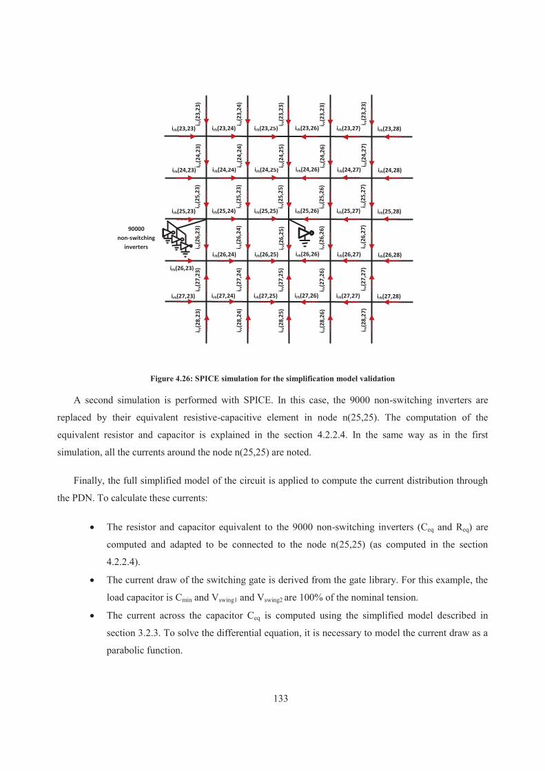
133
irh(26,25) irh(26,24)
irh(26,23)
irh(26,26) irh(26,27) irh(26,28)
irh(27,25) irh(27,24) irh(27,23) irh(27,26) irh(27,27) irh(27,28)
irh(25,25) irh(25,24) irh(25,23) irh(25,26) irh(25,27) irh(25,28)
irh(24,25) irh(24,24) irh(24,23) irh(24,26) irh(24,27) irh(24,28)
irh(23,25) irh(23,24) irh(23,23) irh(23,26) irh(23,27) irh(23,28)
i rv(2
3,2
3)
i rv(2
4,2
3)
i rv(2
5,2
3)
i rv(2
6,2
3)
i rv(2
8,2
3)
,23)
i rv(2
7,2
3)
)
i rv(2
3,2
4)
)
i rv(2
4,2
4)
i rv(2
5,2
3)
i rv(2
6,2
4)
i rv(2
8,2
4)
i rv(2
7,2
4)
,25)
i rv(2
3,2
3)
,25)
i rv(2
4,2
5)
)
i rv(2
5,2
5)
i rv(2
6,2
5)
i rv(2
8,2
5)
i rv(2
7,2
5)
,26)
i rv(2
3,2
3)
,26)
i rv(2
4,2
6)
,26)
i rv(2
5,2
6)
i rv(2
6,2
6)
i rv(2
8,2
6)
i rv(2
7,2
6)
i rv(2
3,2
3)
i rv(2
4,2
7)
i rv(2
5,2
7)
i rv(2
6,2
7)
i rv(2
8,2
7)
i rv(2
7,2
7)
90000
non-switching
inverters
Figure 4.26: SPICE simulation for the simplification model validation
A second simulation is performed with SPICE. In this case, the 9000 non-switching inverters are
replaced by their equivalent resistive-capacitive element in node n(25,25). The computation of the
equivalent resistor and capacitor is explained in the section 4.2.2.4. In the same way as in the first
simulation, all the currents around the node n(25,25) are noted.
Finally, the full simplified model of the circuit is applied to compute the current distribution through
the PDN. To calculate these currents:
· The resistor and capacitor equivalent to the 9000 non-switching inverters (Ceq and Req) are
computed and adapted to be connected to the node n(25,25) (as computed in the section
4.2.2.4).
· The current draw of the switching gate is derived from the gate library. For this example, the
load capacitor is Cmin and Vswing1 and Vswing2 are 100% of the nominal tension.
· The current across the capacitor Ceq is computed using the simplified model described in
section 3.2.3. To solve the differential equation, it is necessary to model the current draw as a
parabolic function.

134
· The current actually drawn from the PDN is the difference between the gate current draw of
the inverter and the current provided by the capacitor (as illustrated in Figure 4.27).
ICeq
time
Ivdd
time
ICeq
time
In(25,25)
n(25,25)
Req
Ceq
Ivdd
Gate library Computed
current across Ceq
Resulting current drawn
at n(25,25) : Ivdd - ICeq
Figure 4.27: Current drawn at node n(25,25)
· The resulting current drawn at the node n(25,25) is injected to the PDN using the distribution
factor. The distribution factor is centered on the node n(25,25) and applied only in the current
window (defined in section 3.1.2, as illustrated in Figure 4.28).
· The correction in the current distribution (computed as explained in section 4.2.2.5) is
applied. The current provided by the capacitor Ceq is used to compute the current distribution
between the original placement of the resistive-capacitive element and its new placement,
using the corresponding distribution correction factor that depends on the original position. In
this case, the 9000 non-switching inverters are connected to the node n(25,23). The
distribution correction factor for n(25,23) is applied in the capacitance window centered on
the node n(25,25) (as illustrated in Figure 4.28).
· The current in the current window is computed:
o Currents inside the capacitance window are computed as the addition of the
percentage of the current drawn from the node n(25,25) determined by the
distribution factor and the percentage of the current across the capacitor determined
by the distribution correction factor.
o Currents outside the capacitance window are the percentage of the current drawn from
the node n(25,25) determined by the distribution factor.

135
Current window
time
ICeq
time
In(25,25)
Computed
current across Ceq
Resulting current drawn
at n(25,25) : Ivdd - ICeq
Dispersion factor Dispersion correction factor
Capacitance
window
n(25,25) n(25,23)
Figure 4.28: Application of the distribution factor and the distribution correction factor for a resistive-capacitive grid.
To validate the simplified model, the first SPICE simulation with 9000 static inverters and the
computed distribution factor using the simplified model are compared. In addition, the currents when the
resistive-capacitive element equivalent to the static gates is connected to the node n(25,25), obtained in the
second SPICE simulation, are also compared to show that the correction in the distribution factor is
necessary.
The currents around the node n(25,25) given by the two SPICE simulations and the computed currents
using the simplified model are plotted in Figure 4.29 (horizontal currents) and Figure 4.30 (vertical
currents). The black curves represent the currents obtained with the first SPICE simulation containing the
9000 non-switching inverters in the node n(25,23), the blue curves correspond to the currents obtained
with the second SPICE simulation when the resistive-capacitive element equivalent to the static gates is
connected to the node n(25,25). Finally, the red curves show the currents computed with the simplified

136
model.
Figure 4.29: Horizontal current distribution
Figure 4.30: Vertical current distribution

137
The first conclusion is that the correction in the distribution factor is indispensable: the differences
between the blue curves and the black curves (taken as a reference) are significant especially in the area
between the node n(25,23) and the node n(25,25). To quantify the deviation generated by the displacement
of the capacitive-elements, the normalized root mean square deviation is calculated for every current
around the node n(25,25). The maximum error is 15.17% in the current across Rv(25,23).
On the other hand, the comparison between the original schematic and the simplified model is made.
As observed in Figure 4.29 and Figure 4.30, a deviation between the simulated and estimated currents is
perceptible in the currents close to the node n(25,23). To quantify the precision of the simplified model,
the normalized root mean square deviation is calculated for every current around the node n(25,25).
Table 4.4 and Table 4.5 contain the computed NRMSD for every horizontal and vertical current. The
maximum error on the estimated current is 6.84% in the current across Rh(25,23). The more significant
errors appear close to the node where the original static gates were connected. NRMSD of the currents
that flow through distant resistors are significantly smaller. In conclusion, the suggested simplified model
including the correction of the distribution factor allows an accurate computation of the current
distribution.
Table 4.4: NRMSD for the horizontal currents (%)
Ih(i,j) 23 24 25 26 27 28
23 4.61 1.82 2.63 2.56 1.16 1.01
24 1.76 2.16 2.16 1.01 0.84 0.86
25 6.84 2.91 1.62 0.85 0.79 0.80
26 1.76 2.16 2.16 1.01 0.84 0.86
27 4.61 1.82 2.63 2.56 1.16 1.01
Table 4.5: NRMSD for the vertical currents (%)
Iv(i,j) 23 24 25 26 27
23 2.83 1.30 0.81 0.78 0.78
24 5.64 1.30 0.81 0.82 0.80
25 6.06 1.30 0.99 0.94 0.87
26 6.06 1.30 0.99 0.94 0.87
27 5.64 1.30 0.81 0.82 0.80
28 2.83 1.30 0.81 0.78 0.78

138

139
5 General conclusion and future work
Continuous scaling in deep-submicron technologies has reduced progressively the supply voltage and
increased the number of transistors in the ICs. Consequently supply voltage noise has increased,
negatively impacting the performance and reliability of the chips. Power supply noise has therefore
become a critical concern, both for design and test aspects. One of the most important sources of supply
voltage drop is the IR-Drop; a phenomenon intrinsically related to the resistive elements of the PDN and
the switching activity. This work was concerned by the modeling and simulation of logic circuits in the
context of IR-drop induced delay.
This document has proposed an original algorithm for an event-driven mixed-mode simulation of the
IR-Drop. This algorithm takes into account the different characteristics of the IR-Drop. Indeed, the
simulation involves an electrical simulation and a logic simulation. For this reason, we have developed
accurate and efficient electrical models for the currents generated by the switching gates, the propagation
of these currents through the PDN and the gate delays.
Chapter 2 described the modeling procedure for all the electrical parameters of the logic gate that are
required in the simulator: static currents, dynamic currents and gate delays. The three elements are highly
dependent on the transistor electrical parameters and thus, a library pre-characterization is required for
every technology. There are also other variable parameters involved in the modeling process: the input
voltage swing Vswing1, the switching gate supply voltage swing Vswing2 and the output capacitance Cload.
SPICE simulations have been performed for all possible combinations of Vswing1, Vswing2 and Cload. As a
result, a model was derived to compute the static currents, the dynamic currents and the delays for any
electrical configuration. Since the current draw generated by a switching gate lasts a limited amount of
time, a time window of 100ps is used for the current draw model.

140
Current distribution is closely related to the PDN structure and thus, a model for the PDN has been
proposed to estimate the current distribution in Chapter 3. Because the IR-Drop involves the resistive
elements, the PDN is modelled as a resistive two-dimensional grid. Based on this model, different
distribution factors depending on the position in the grid are computed. These distribution factors allow to
estimate the fraction of current that flows through every resistance of the grid and then, to compute the
voltage in every node of the grid. In addition, a current window is determined in order to reduce the
simulation time: the simulation only takes into account fractions of current higher than 1% of the original
current draw. In addition, an electrical model to take into account the voltage drop generated by the
neighbouring block is proposed. As a result, the voltage drop is considered as a global phenomenon at the
chip level.
In Chapter 4 the proposed algorithm was explained in details. Logic and electrical simulations are
running concurrently and communicate through the switching events. The logic simulation sends input
switching events to the electrical simulation. The electrical simulation estimates the voltage drop in the
node of the resistive grid where the gate is connected, using the dispersion factor and taking into account
all the currents generated by the precedent switching gates. Then, the simulator derives the current draw
and the gate delay in function of the input voltage swing Vswing1, the supply voltage swing Vswing2 and the
output capacitance Cload. Finally, the estimated current draws at Vdd and Gnd are noted in the event queue
and a switching output event that considers the estimated gate delay is sent to the logic simulation.
Using the electrical models proposed in this work, the University of Passau has developed a Mixed-
mode IR-drop Induced Delay simulator (MIRID). In order to validate the electrical models, waveforms
and induced delay obtained from MIRID and from SPICE simulations have been compared for different
circuits. Note that large circuits cannot be simulated with SPICE but voltage drop generated by small
circuits is not enough to generate significant induced delay. For this reason, a macro-cell structure was
proposed to increase the voltage drop and consequently, validate the IR-Drop induced delay estimation.
Although this work originally tackles the IR-Drop phenomenon, Chapter 3 presented an extension that
includes capacitive elements of the PDN in the electrical model in order to analyze the impact of these
capacitive elements on the current distribution. An electrical model has been described for the three types
of capacitive elements present in the PDN: parasitic capacitors of the physical PDN, intentional
decoupling capacitors and intrinsic decoupling capacitors due to non-switching gates.
From the above analysis we have concluded that the presence of capacitive elements reduces the
voltage drop propagation in space and that the voltage drop dissipates slowly over time. In addition,
we have concluded that the impact of the capacitance elements on current distribution decreases when the

141
distance increases. The further away from the switching gate they are, the smaller the amount of current
provided and demanded by the capacitor. Thus, a capacitance window can be used to determine the
capacitive elements that are relevant in the current distribution.
A mathematical estimation of the current distribution through a resistive grid with capacitive elements
is very complex. Using simplifications, a method was proposed to compute the current distribution. It
allows to define a single lumped capacitive element connected to the node where the switching gate is
connected, which is equivalent to all the capacitive elements into the capacitance window. The
contribution of the single capacitance is calculated by a differential equation. As a result, the current
drawn at the node from the PDN is the difference between the current draw of the gate and the current
provided by the single capacitance. A maximal error of 3.4% in the current distribution estimation is
obtained in the preliminary simulations applying the simplified model.
Thanks to the electrical modelling, an extensive analysis of the electrical parameters involved in the
IR-Drop phenomenon has been presented in this document. In addition, the impact of the voltage drop due
to the IR-Drop and its propagation through the PDN has been also analysed. This knowledge may be very
useful in order to tackle the future works about the IR-Drop. In the short term, the future work must be
focused on improving the electrical models used in the simulation and developing a new simulator version
that includes the capacitive elements in the PDN model. In the long term, MIRID can be used as an
accurate tool to simulate test sequences and to determine the induced delay due to the IR-Drop. Note that
MIRID can simulate test sequences oriented to detect delay faults or other types of faults (stuck-at faults,
bridging faults, etc.). In the context of the IR-Drop, MIRID can be used as an analysis tool. The
information obtained can be used to develop new test pattern generation methods to test the timing faults
due to the IR-Drop or other types of faults.

142

143
Annex
Complete table of NRMSD of the dynamical current model, explained in section 2.3.2.
Table A.1: Compete table of the NRMSD of the current draw model
Gate Input vector Switching input Cload Current Vdd:
average NRMSD (%)
Current Gnd:
average NRMSD (%)
INV 0/ 1 In 1: Rising edge 1Cmin 0.3198 1.8845
INV 0/ 1 In 1: Rising edge 2Cmin 0.4026 2.6482
INV 0/ 1 In 1: Rising edge 3Cmin 0.2998 3.9139
INV 0/ 1 In 1: Rising edge 4Cmin 0.2394 4.5671
INV 0/ 1 In 1: Rising edge 5Cmin 0.2375 5.1877
INV 1/0 In 1: Falling edge 1Cmin 1.4209 0.4151
INV 1/0 In 1: Falling edge 2Cmin 2.0467 0.2045
INV 1/0 In 1: Falling edge 3Cmin 2.5305 0.1846
INV 1/0 In 1: Falling edge 4Cmin 2.9270 0.1672
INV 1/0 In 1: Falling edge 5Cmin 3.1532 0.1557
BUF 0/1 In 1: Rising edge 1Cmin 1.6808 1.2412
BUF 0/ 1 In 1: Rising edge 2Cmin 1.1576 1.2156
BUF 0/ 1 In 1: Rising edge 3Cmin 0.8535 0.7053
BUF 0/ 1 In 1: Rising edge 4Cmin 0.9773 0.6457
BUF 0/ 1 In 1: Rising edge 5Cmin 1.0635 0.5160
BUF 1/1 In 1: Falling edge 1Cmin 1.6808 1.2412
BUF 1/1 In 1: Falling edge 2Cmin 1.1576 1.2156
BUF 1/1 In 1: Falling edge 3Cmin 0.9734 1.2507
BUF 1/1 In 1: Falling edge 4Cmin 0.5781 1.2168
BUF 1/1 In 1: Falling edge 5Cmin 0.3871 1.1214
NAND4 0111/1111 In 1: Rising edge 1Cmin 0.3470 0.8040
NAND4 0111/1111 In 1: Rising edge 2Cmin 0.3437 1.0029
NAND4 0111/1111 In 1: Rising edge 3Cmin 0.3366 1.130
NAND4 0111/1111 In 1: Rising edge 4Cmin 0.3335 1.1576
NAND4 0111/1111 In 1: Rising edge 5Cmin 0.3332 1.1656
NAND3 011/111 In 1: Rising edge 1Cmin 0.3541 0.8537
NAND3 011/111 In 1: Rising edge 2Cmin 0.3291 0.8893
NAND3 011/111 In 1: Rising edge 3Cmin 0.3055 0.6658

144
NAND3 011/111 In 1: Rising edge 4Cmin 0.2835 0.7184
NAND3 011/111 In 1: Rising edge 5Cmin 0.2297 1.1442
NAND2 01/11 In 1: Rising edge 1Cmin 0.3761 0.8612
NAND2 01/11 In 1: Rising edge 2Cmin 0.3909 1.0194
NAND2 01/11 In 1: Rising edge 3Cmin 0.2494 1.1431
NAND2 01/11 In 1: Rising edge 4Cmin 0.2524 1.5815
NAND2 01/11 In 1: Rising edge 5Cmin 0.3493 1.8745
NAND4 1111/0111 In 1: Falling edge 1Cmin 0.7134 0.4428
NAND4 1111/0111 In 1: Falling edge 2Cmin 1.9991 0.3448
NAND4 1111/0111 In 1: Falling edge 3Cmin 1.4447 0.3385
NAND4 1111/0111 In 1: Falling edge 4Cmin 1.0174 0.3272
NAND4 1111/0111 In 1: Falling edge 5Cmin 0.8210 0.3152
NAND3 111/011 In 1: Falling edge 1Cmin 0.4730 0.3927
NAND3 111/011 In 1: Falling edge 2Cmin 0.7115 0.5136
NAND3 111/011 In 1: Falling edge 3Cmin 2.1552 0.4177
NAND3 111/011 In 1: Falling edge 4Cmin 2.3699 0.3614
NAND3 111/011 In 1: Falling edge 5Cmin 1.6668 0.3535
NAND2 11/01 In 1: Falling edge 1Cmin 0.6843 0.2186
NAND2 11/01 In 1: Falling edge 2Cmin 0.7256 0.2164
NAND2 11/01 In 1: Falling edge 3Cmin 1.0119 0.1953
NAND2 11/01 In 1: Falling edge 4Cmin 0.7918 0.1707
NAND2 11/01 In 1: Falling edge 5Cmin 2.5833 0.1969
NAND4 1011/1111 In 2: Rising edge 1Cmin 0.4879 1.2089
NAND4 1011/1111 In 2: Rising edge 2Cmin 0.4737 1.3986
NAND4 1011/1111 In 2: Rising edge 3Cmin 0.4624 1.4984
NAND4 1011/1111 In 2: Rising edge 4Cmin 0.4621 1.6078
NAND4 1011/1111 In 2: Rising edge 5Cmin 0.4626 1.7695
NAND3 101/111 In 2: Rising edge 1Cmin 0.4713 1.1208
NAND3 101/111 In 2: Rising edge 2Cmin 0.4619 1.4444
NAND3 101/111 In 2: Rising edge 3Cmin 0.4801 1.5536
NAND3 101/111 In 2: Rising edge 4Cmin 0.4858 1.6074
NAND3 101/111 In 2: Rising edge 5Cmin 0.5063 1.7128
NAND2 10/11 In 2: Rising edge 1Cmin 1.4158 2.0656
NAND2 10/11 In 2: Rising edge 2Cmin 1.1813 2.321
NAND2 10/11 In 2: Rising edge 3Cmin 1.0537 2.4875
NAND2 10/11 In 2: Rising edge 4Cmin 1.1476 3.1315
NAND2 10/11 In 2: Rising edge 5Cmin 1.2716 3.7823
NAND4 1111/1011 In 2: Falling edge 1Cmin 0.2239 0.3242
NAND4 1111/1011 In 2: Falling edge 2Cmin 0.2199 0.2713
NAND4 1111/1011 In 2: Falling edge 3Cmin 0.8490 0.2203
NAND4 1111/1011 In 2: Falling edge 4Cmin 0.9291 0.1920
NAND4 1111/1011 In 2: Falling edge 5Cmin 0.6561 0.1766
NAND3 111/101 In 2: Falling edge 1Cmin 0.3580 0.3395
NAND3 111/101 In 2: Falling edge 2Cmin 0.3305 0.2461
NAND3 111/101 In 2: Falling edge 3Cmin 0.3482 0.2031
NAND3 111/101 In 2: Falling edge 4Cmin 0.6310 0.1742
NAND3 111/101 In 2: Falling edge 5Cmin 0.8484 0.1547
NAND2 11/10 In 2: Falling edge 1Cmin 0.5155 0.3823
NAND2 11/10 In 2: Falling edge 2Cmin 0.5148 0.2265

145
NAND2 11/10 In 2: Falling edge 3Cmin 0.6493 0.1789
NAND2 11/10 In 2: Falling edge 4Cmin 1.2795 0.1563
NAND2 11/10 In 2: Falling edge 5Cmin 1.3052 0.1544
NAND4 1101/1111 In 3: Rising edge 1Cmin 2.3316 1.3808
NAND4 1101/1111 In 3: Rising edge 2Cmin 2.2684 1.7386
NAND4 1101/1111 In 3: Rising edge 3Cmin 2.2136 2.0173
NAND4 1101/1111 In 3: Rising edge 4Cmin 2.1679 2.2536
NAND4 1101/1111 In 3: Rising edge 5Cmin 2.1294 2.4641
NAND3 110/111 In 3: Rising edge 1Cmin 2.0135 1.9311
NAND3 110/111 In 3: Rising edge 2Cmin 2.0068 2.5634
NAND3 110/111 In 3: Rising edge 3Cmin 1.9904 3.0461
NAND3 110/111 In 3: Rising edge 4Cmin 1.9397 3.5036
NAND3 110/111 In 3: Rising edge 5Cmin 1.9255 4.0419
NAND4 1111/1101 In 3: Falling edge 1Cmin 0.4023 0.3691
NAND4 1111/1101 In 3: Falling edge 2Cmin 0.3917 0.1173
NAND4 1111/1101 In 3: Falling edge 3Cmin 0.2855 0.04960
NAND4 1111/1101 In 3: Falling edge 4Cmin 0.4618 0.08620
NAND4 1111/1101 In 3: Falling edge 5Cmin 0.2783 0.04400
NAND3 111/110 In 3: Falling edge 1Cmin 0.9346 0.2218
NAND3 111/110 In 3: Falling edge 2Cmin 0.6506 0.1567
NAND3 111/110 In 3: Falling edge 3Cmin 0.6847 0.1168
NAND3 111/110 In 3: Falling edge 4Cmin 0.9576 0.2192
NAND3 111/110 In 3: Falling edge 5Cmin 1.5883 0.4002
NAND4 1110/1111 In 4: Rising edge 1Cmin 2.7663 2.1682
NAND4 1110/1111 In 4: Rising edge 2Cmin 2.9087 2.7267
NAND4 1110/1111 In 4: Rising edge 3Cmin 2.9932 3.2404
NAND4 1110/1111 In 4: Rising edge 4Cmin 3.0476 3.8167
NAND4 1110/1111 In 4: Rising edge 5Cmin 3.0647 4.3224
NAND4 1111/1110 In 4: Falling edge 1Cmin 1.1331 0.4199
NAND4 1111/1110 In 4: Falling edge 2Cmin 1.5753 0.3529
NAND4 1111/1110 In 4: Falling edge 3Cmin 1.2951 0.2764
NAND4 1111/1110 In 4: Falling edge 4Cmin 0.9256 0.2404
NAND4 1111/1110 In 4: Falling edge 5Cmin 1.1751 0.3994
NOR4 0010/0000 In 3: Falling edge 1Cmin 0.5374 1.8113
NOR4 0010/0000 In 3: Falling edge 2Cmin 0.3639 2.0159
NOR4 0010/0000 In 3: Falling edge 3Cmin 0.4618 2.2004
NOR4 0010/0000 In 3: Falling edge 4Cmin 0.4727 3.6431
NOR4 0010/0000 In 3: Falling edge 5Cmin 0.4363 2.8243
NOR4 0000/0010 In 3: Rising edge 1Cmin 0.6859 0.2293
NOR4 0000/0010 In 3: Rising edge 2Cmin 0.9612 0.2080
NOR4 0000/0010 In 3: Rising edge 3Cmin 1.0353 0.2004
NOR4 0000/0010 In 3: Rising edge 4Cmin 1.2971 0.1897
NOR4 0000/0010 In 3: Rising edge 5Cmin 1.5188 0.1450
NOR4 0000/0001 In 4: Rising edge 1Cmin 0.5458 2.0979
NOR4 0000/0001 In 4: Rising edge 2Cmin 0.3573 2.208
NOR4 0000/0001 In 4: Rising edge 3Cmin 0.4779 1.7126
NOR4 0000/0001 In 4: Rising edge 4Cmin 0.4784 1.9594
NOR4 0000/0001 In 4: Rising edge 5Cmin 0.4500 2.1764
NOR4 0001/0000 In 4: Falling edge 1Cmin 0.8233 0.2106

146
NOR4 0001/0000 In 4: Falling edge 2Cmin 0.9897 0.1861
NOR4 0001/0000 In 4: Falling edge 3Cmin 1.4074 0.1727
NOR4 0001/0000 In 4: Falling edge 4Cmin 1.6072 0.1595
NOR4 0001/0000 In 4: Falling edge 5Cmin 1.7924 0.1654
NOR3 000/001 In 3: Rising edge 1Cmin 0.2551 0.7337
NOR3 000/001 In 3: Rising edge 2Cmin 0.1719 1.3203
NOR3 000/001 In 3: Rising edge 3Cmin 0.1455 0.9824
NOR3 000/001 In 3: Rising edge 4Cmin 0.1390 0.6844
NOR3 000/001 In 3: Rising edge 5Cmin 0.1344 0.5282
NOR3 001/000 In 3: Falling edge 1Cmin 0.6164 0.5246
NOR3 001/000 In 3: Falling edge 2Cmin 0.4089 1.5231
NOR3 001/000 In 3: Falling edge 3Cmin 0.4784 1.6886
NOR3 001/000 In 3: Falling edge 4Cmin 0.4744 1.6795
NOR3 001/000 In 3: Falling edge 5Cmin 0.4510 1.571
NOR4 0000/0100 In 2: Rising edge 1Cmin 0.5274 1.6216
NOR4 0000/0100 In 2: Rising edge 2Cmin 0.3316 2.3088
NOR4 0000/0100 In 2: Rising edge 3Cmin 0.4543 1.8965
NOR4 0000/0100 In 2: Rising edge 4Cmin 0.4746 2.0556
NOR4 0000/0100 In 2: Rising edge 5Cmin 0.4522 2.6831
NOR3 000/010 In 2: Rising edge 1Cmin 1.4558 1.6867
NOR3 000/010 In 2: Rising edge 2Cmin 1.6773 1.5655
NOR3 000/010 In 2: Rising edge 3Cmin 1.7796 1.6054
NOR3 000/010 In 2: Rising edge 4Cmin 1.7313 1.6271
NOR3 000/010 In 2: Rising edge 5Cmin 1.8161 1.6369
NOR2 00/01 In 2: Rising edge 1Cmin 2.3716 1.3795
NOR2 00/01 In 2: Rising edge 2Cmin 1.6713 1.527
NOR2 00/01 In 2: Rising edge 3Cmin 1.8547 1.5313
NOR2 00/01 In 2: Rising edge 4Cmin 2.2648 1.3398
NOR2 00/01 In 2: Rising edge 5Cmin 2.3932 1.1104
NOR4 0100/0000 In 2: Falling edge 1Cmin 1.0208 0.2088
NOR4 0100/0000 In 2: Falling edge 2Cmin 1.1781 0.1803
NOR4 0100/0000 In 2: Falling edge 3Cmin 1.9611 0.1634
NOR4 0100/0000 In 2: Falling edge 4Cmin 1.9979 0.1527
NOR4 0100/0000 In 2: Falling edge 5Cmin 2.119 0.1459
NOR3 010/000 In 2: Falling edge 1Cmin 0.1207 0.7596
NOR3 010/000 In 2: Falling edge 2Cmin 0.1536 0.7373
NOR3 010/000 In 2: Falling edge 3Cmin 0.2008 0.7838
NOR3 010/000 In 2: Falling edge 4Cmin 0.1608 0.8374
NOR3 010/000 In 2: Falling edge 5Cmin 0.1307 0.8870
NOR2 01/00 In 2: Falling edge 1Cmin 0.2323 1.1589
NOR2 01/00 In 2: Falling edge 2Cmin 0.1463 1.6658
NOR2 01/00 In 2: Falling edge 3Cmin 0.1602 1.3492
NOR2 01/00 In 2: Falling edge 4Cmin 0.1556 1.0585
NOR2 01/00 In 2: Falling edge 5Cmin 0.1486 0.9179
NOR4 0000/1000 In 1: Rising edge 1Cmin 0.2564 0.5000
NOR4 0000/1000 In 1: Rising edge 2Cmin 0.3944 1.9214
NOR4 0000/1000 In 1: Rising edge 3Cmin 0.5004 2.1723
NOR4 0000/1000 In 1: Rising edge 4Cmin 0.5057 2.2549
NOR4 0000/1000 In 1: Rising edge 5Cmin 0.4880 2.2015

147
NOR3 000/100 In 1: Rising edge 1Cmin 1.729 0.8017
NOR3 000/100 In 1: Rising edge 2Cmin 2.4428 0.7842
NOR3 000/100 In 1: Rising edge 3Cmin 3.3468 0.7776
NOR3 000/100 In 1: Rising edge 4Cmin 3.760 0.7675
NOR3 000/100 In 1: Rising edge 5Cmin 4.1451 0.7724
NOR2 00/10 In 1: Rising edge 1Cmin 2.0047 0.9736
NOR2 00/10 In 1: Rising edge 2Cmin 1.8563 1.421
NOR2 00/10 In 1: Rising edge 3Cmin 1.8607 1.6457
NOR2 00/10 In 1: Rising edge 4Cmin 1.9983 1.7171
NOR2 00/10 In 1: Rising edge 5Cmin 2.4373 1.7666
NOR4 1000/0000 In 1: Falling edge 1Cmin 2.1266 1.3187
NOR4 1000/0000 In 1: Falling edge 2Cmin 3.0438 1.2187
NOR4 1000/0000 In 1: Falling edge 3Cmin 3.0057 0.8174
NOR4 1000/0000 In 1: Falling edge 4Cmin 3.1374 0.5565
NOR4 1000/0000 In 1: Falling edge 5Cmin 3.2600 0.4003
NOR3 100/000 In 1: Falling edge 1Cmin 0.5417 0.5445
NOR3 100/000 In 1: Falling edge 2Cmin 0.3858 1.1446
NOR3 100/000 In 1: Falling edge 3Cmin 0.4326 1.3286
NOR3 100/000 In 1: Falling edge 4Cmin 0.4114 1.4539
NOR3 100/000 In 1: Falling edge 5Cmin 0.4087 1.6681
NOR2 10/00 In 1: Falling edge 1Cmin 1.5765 1.2808
NOR2 10/00 In 1: Falling edge 2Cmin 1.4248 0.7475
NOR2 10/00 In 1: Falling edge 3Cmin 2.0625 0.4822
NOR2 10/00 In 1: Falling edge 4Cmin 2.6643 0.3801
NOR2 10/00 In 1: Falling edge 5Cmin 2.8578 0.3560

148

149
TABLE OF FIGURES
Figure 1.1: A current draw injected into a power grid dissipates quickly in time (a) and
space (b) [7]. ...................................................................................................................... 17
Figure 1.2: General structure of the simulator ...................................................................................... 28
Figure 1.3: Functional view of the simulation algorithm ...................................................................... 29
Figure 1.4: Didactic view of the mixed-mode simulation .................................................................... 30
Figure 1.5: PDN topology ..................................................................................................................... 33
Figure 2.1: Inverter transfer curve ........................................................................................................ 36
Figure 2.2: Transistor operating regions of an inverter (down transition) ............................................ 37
Figure 2.3: Dynamic currents in the inverter ........................................................................................ 38
Figure 2.4: Static currents in the inverter .............................................................................................. 39
Figure 2.5: Inverter transfer curve and noise margins. ......................................................................... 40
Figure 2.6: Library variable parameters definition ............................................................................... 42
Figure 2.7: Pre-characterization electrical schematic for an inverter ................................................... 43
Figure 2.8: Library electrical parameters definition ............................................................................. 45
Figure 2.9: Inverter delay variations in function of voltage swings and load capacitance ................... 46
Figure 2.10: Variation of the delay as a function of Vswing1 and Vswing2 with Cmin load obtained
from Spice simulation (left) and computed from MLR function (right). ........................ 47
Figure 2.11: Dynamic current model arrays ......................................................................................... 49
Figure 2.12: Variation of the transient current draw for different values of a)the power swing;
b) the input swing; c) the load capacitance ..................................................................... 50
Figure 2.13: Static currents in the inverter (low input) ......................................................................... 53
Figure 2.14: Static current of an inverter in function of Vinput and Vswing2 ............................................ 54
Figure 2.15: Static current in Vdd of an inverter in function of Vinput and Vswing2 ................................ 55
Figure 2.16: Static current of an inverter when Vswing1 = Vswing2 ........................................................... 56
Figure 2.17: Schematic for self-IR-Drop simulation ............................................................................ 58
Figure 2.18: Self IR-Drop simulation of an inverter ............................................................................. 59
Figure 3.1: PDN resistive model ........................................................................................................... 63
Figure 3.2: Currents and nodes in the symbolic grid ............................................................................ 63
Figure 3.3: Example of SPICE simulations to determine the distribution factor .................................. 64

150
Figure 3.4: Distribution factor matrixes ................................................................................................ 66
Figure 3.5: Horizontal distribution factor in the 100x100 grid in the central area ............................... 67
Figure 3.6: Horizontal and vertical dispersion factors in the central area ............................................ 68
Figure 3.7: Maximum relative error between the current distributions simulated with SPICE
and computed with the central distribution factor (horizontal resistors) ........................... 69
Figure 3.8: The three different distribution areas: central, band and corner areas. ............................... 70
Figure 3.9: Maximum relative error between the current distributions simulated with SPICE
and computed with the corner distribution factor (horizontal resistors) ............................ 71
Figure 3.10: Maximum relative error between the current distributions simulated with SPICE
and computed with the band distribution factor (horizontal resistors) ............................ 71
Figure 3.11: Horizontal dispersion factor in the corner area ................................................................ 72
Figure 3.12: Horizontal dispersion factor in the band area ................................................................... 72
Figure 3.13: Pre-characterization of the PDN grid taking into account the influence of the
neighboring blocks. ......................................................................................................... 73
Figure 3.14: Equivalent grid resistance vs grid size and elementary grid resistance value .................. 74
Figure 3.15: Equivalent grid resistance vs elementary grid resistance (left) and equivalent grid
resistance vs grid size (right)........................................................................................... 75
Figure 3.16: Simulation of the resistive PDN with a single capacitor .................................................. 78
Figure 3.17: Currents and voltages in the simplified resistive PDN model .......................................... 78
Figure 3.18: Currents and voltages in the simplified resistive and capacitive PDN model .................. 79
Figure 3.19: Current across the capacitor and voltage in node n2 ......................................................... 79
Figure 3.20: Current across each element and voltage in each node .................................................... 80
Figure 3.21: Capacitor discharge and charge phases. ........................................................................... 81
Figure 3.22: Simplified resistive and capacitive PDN with five capacitors ......................................... 82
Figure 3.23: Simulation current and voltage waveforms for a multi-capacitor PDN. .......................... 83
Figure 3.24: Current draw vs current provided by the voltage source with/without capacitive
elements .......................................................................................................................... 84
Figure 3.25: Signed area of the regions in the xy-plane bounded by Idraw and IVsource ........................... 85
Figure 3.26: Generic schematic for the mathematical analysis............................................................. 87
Figure 3.27: Parabolic function approximation for the current draw.................................................... 89
Figure 3.28: Simulated and computed current across the capacitor CS ................................................ 92
Figure 3.29: Average NRMSD of PDN currents with and without grid capacitors.............................. 94
Figure 3.30: NRMSD contour for PDN currents with and without grid capacitors.............................. 94
Figure 3.31: Gates input capacitances and interconnection capacitance connected to a node .............. 95

151
Figure 3.32: Electrical model for the non-switching gates ................................................................... 96
Figure 4.1: Mixed-mode simulator ....................................................................................................... 99
Figure 4.2: Schematic of 14-inverter chain validation ........................................................................ 103
Figure 4.3: Validation electrical waveforms in node and resistor (40,50) for a 14-inverter
chain (ps precision) .......................................................................................................... 104
Figure 4.4: Validation electrical waveforms in node and resistor (60,50) for a 14-inverter
chain (ps precision) .......................................................................................................... 104
Figure 4.5: Validation electrical waveforms in node and resistor (50,50) for c17 (ps precision) ....... 106
Figure 4.6: Validation electrical waveforms in node and resistor (50,50) for c17 (0.1ps precision) .. 107
Figure 4.7: Variation of the current draw for the different output capacitance values ....................... 108
Figure 4.8: Dedicated circuit to enhance the IR-Drop: logic schematic and PDN connection ........... 110
Figure 4.9: IR-drop delay in function of the number of inverter chains in parallel for MIRID
and SPICE........................................................................................................................ 111
Figure 4.10: Current distribution through the R grid vs current distribution through RC grid ........... 112
Figure 4.11: Standard resistive grid with parasitic resistive and capacitive elements (RC grid) ........ 114
Figure 4.12: Radius of the capacitance window ................................................................................. 115
Figure 4.13: Detail of the radius of the capacitance window .............................................................. 115
Figure 4.14: Simplified model of the capacitive-resistive grid ........................................................... 117
Figure 4.15: Contribution of a capacitive element in the current distribution (different phases
in time) .......................................................................................................................... 118
Figure 4.16: Contribution of a capacitive element in the current distribution (impact of the
simplification) ............................................................................................................... 119
Figure 4.17: Simplification method for RC-PDN model .................................................................... 120
Figure 4.18: Resistive-capacitive element connected to the node n(i,j) ............................................. 121
Figure 4.19: Resistive-capacitive element connected to the node n(m,n) and its equivalent
displaced to the node n(r,s) ........................................................................................... 123
Figure 4.20: Equivalent resistor calculation example ......................................................................... 126
Figure 4.21: Example for the validation of the equivalent resistor and capacitor calculation ............ 127
Figure 4.22: Validation of the equivalent resistor and capacitor calculation ...................................... 129
Figure 4.23: Pre-characterization of the distribution correction factor ............................................... 130
Figure 4.24: Distribution correction factor for the node n(50,48) ...................................................... 131
Figure 4.25: Distribution correction factor for the node n(48,48) ...................................................... 132
Figure 4.26: SPICE simulation for the simplification model validation ............................................. 133
Figure 4.27: Current drawn at node n(25,25)...................................................................................... 134

152
Figure 4.28: Application of the distribution factor and the distribution correction factor for a
resistive-capacitive grid. ............................................................................................... 135
Figure 4.29: Horizontal current distribution ....................................................................................... 136
Figure 4.30: Vertical current distribution ........................................................................................... 136

153
LIST OF TABLES
Table 2.1: Regions of operation of transistors in a symmetrical CMOS inverter ................................. 37
Table 2.2: Regression coefficients for the delay computation of an inverter. ...................................... 47
Table 2.3: Delay model error. ............................................................................................................... 48
Table 2.4: NRMSD of the current draw model (extract). ..................................................................... 51
Table 2.5: Simulated static currents in 45nm technology under nominal conditions ........................... 53
Table 4.1: NRMSD error for voltage and current estimation for a chain of 14 inverters (in the
example nodes and resistors) ........................................................................................... 105
Table 4.2: NRMSD error for voltage and current estimation for c17 in node and resistor (50,50) .... 106
Table 4.3: NRMSD error for voltage and current estimation for c17 in node and resistor (50,50)
(with 0.1ps precision) ...................................................................................................... 107
Table 4.4: NRMSD for the horizontal currents (%) ............................................................................ 137
Table 4.5: NRMSD for the vertical currents (%) ................................................................................ 137
Table A.1: Compete table of the NRMSD of the current draw model ............................................... 143

154

155
REFERENCES
[1] K.L. Shepard and V. Narayanan, “Noise in Deep Submicrom Digital Design”, Computer-Aided Design,
Proceedings of ICCAD/IEEE, pp.524-531, San Jose, CA, USA, 1996.
[2] H.H. Chen and D.D. Ling, “Power Supply Noise Analysis Methodology for Deep Submicron VLSI
Design”, Design Automation Conference, Proceedings of the 34th ACM/IEEE, pp.638-643, Anaheim,
CA, USA, 1997.
[3] Y.M. Jiang and K.T. Cheng, “Analysis of Performance Impact Caused by Power Supply Noise in Deep
Submicron Devices”, Design Automation Conference, Proceedings of the 36th ACM/IEEE, pp.760-
765, New Orleans, LA ,USA, 1999.
[4] R. Saleh, S. Z. Hussain, S. Rochel, and D. Overhauser, “Clock skew verification in the presence of IR-
Drop in the power distribution network”, Computer-Aided Design of Integrated Circuits and Systems,
vol. 19, No. 6, pp.635-644, 2000.
[5] S. Pant, D. Blaauw, V. Zolotov, S. Sundareswaran, and R. Panda, “Vectorless Analysis of Supply
Noise Induced Delay Variation”, Proceedings of IEEE International Conference on Computer-Aided
Design, pp 184-191, 2003.
[6] C. Tirumurti, S. Kundu, S. K. Susmita, and Y. S. Change, “A Modeling Approach for Addressing
Power Supply Switching Noise Related Failures of Integrated Circuits” Proceedings of Design,
Automation and Test in Europe Conference, pp. 1078-1083, 2004.
[7] S. Pant, E. Chiprout ;”Power grid physics and implications for CAD”, Design Automation Conference,
San Francisco, Proceedings of 43rd Design Automation Conference ACM/IEEE, LA, USA 2006
[8] P. Guptaa and A.B. Kahng; “Efficient Design and Analysis of Robust Power Distribution
Meshes”, 19th International Conference on VLSI Design, Pages 337-342, 2006
[9] L.H. Chen, M. Marek-Sadowska, and F. Brewer; “Coping with Buffer Delay change due to Power ans
Ground Noise,” In Proceeding of Design Automation Conference, pp. 860 – 865, New Orleans, LA,
USA, 2002.
156
[10] A. Todri, A. Bosio, L. Dilillo, P. Girard, S. Pravossoudovitch, A. Virazel,” A Study of the Path Delay
variations in the presence of Uncorrelated Power and Ground Supply Noise”, Design and diagnostics of
electronic circuits & systems (DDECS), pp. 189 - 194 , Cottbus , Germany, 2011
[11] R. Panda, D. Blaauw, R. Chaudhry, V. Zolotov, B. Young, R. Ramaraju; ”Model and Analysis for
Combined Package and on-chip Power Grid Simulation”, Low Power Electronics and Design, pp. 179
– 184, 2000
[12] Jing-Jia Liou; Krstic, A.; Yi-Min Jiang; Kwang-Ting Cheng; “Path selection and pattern generation for
dynamic timing analysis considering power supply noise effects” International conference Computer
Aided Design, Pages 493 – 496, San Jose, CA, USA 2000
[13] Yi-Min Jiang; Kwang-Ting Cheng; An-Chang Deng; “Estimation of maximum Power supply noise for
deep sub-micron design” Low Power Electronics and Design6 , Pages 233 - 238 , Monterey, CA, USA
,1998
[14] Krstic, A.; Yi-Min Jiang; Kwang-Ting Cheng; “Pattern Generation for delay testing and dynamic
timing analysis considering power supply noise effects” Computer-Aided Design of Integrated Circuits
and Systems, Pages 416 - 425, 2001
[15] Shiyou Zhao , Kaushik Roy , Cheng-kok Koh, “Estimation of inductive and resistive switching noise
on power supply network in deep sub-micron CMOS circuits ” , International Conference on Computer
Design,Pages 65 - 72 ,Austin, TX,USA ,2000
[16] G. Bai, S. Bodda and I. N. Hajj, “Static Timing Analysis Including Power Supply Noise Effect on
Propagation Delay in VLSI Circuits,” ACM/IEEE Design Automation Conf. , pp. 295-300, Las Vegas,
NV, USA, June 2001.
[17] H. Kriplani, F. N. Najm, and I. N. Hajj; “Pattern Independent Maximum Current Estimation in Power
and Ground Buses of CMOS VLSI Circuits: Algorithms, Signal Correlations, and Their
Resolution,”TCAD, pp. 998-1012, August 1995.
[18] L.-C. Wang, Qiu Wangqi, S.Fancler, D.M.H. Walker; ”Static compaction of delay tests considering
power supply noise”, VLSI Test Symposium, pp: 235-240, May 2005
[19] P. Larsson; “Power Supply Noise in Future IC’s: A Cristal Ball Reading,” in Proc. IEEE Custom
Integr. Circuits Conf., pp. 467-474, San Diego, CA, USA, 1999
[20] S. Zhao, K. Roy and K. K. Cheng; “Decoupling capacitance allocation and its application to power-
supply noise-aware floorplanning” IEEE Trans. Comput.- Aided Design Integr. Circuits Syst., vol. 21,
no. 1, pp. 81-92, Jan. 2002.

157
[21] H. M. Chen, L. D. Huang, I. M. Liu, M. Lai and D. F. Wong; “Floorplanning with Power Supply Noise
Avoidance” in Proc. Design Autom. Conf. Asia and South Pacific (ASP-DAC), pp. 427-430, Jan. 2003
[22] S. A. Moghaddam, N. Masoumi and C. Lucas; “A Stochastic Power-supply Noise Reduction Technique
Using Max-flow Algorithm and Decoupling Capacitance” in Proc. Int. Workshop System-on-Chip
Real-Time Applications, pp. 265-269 , July 2005
[23] J. Gu, R. Harjani and C. Kim; “Distributed Active Decoupling Capacitors for On-Chip Supply Noise
Cancellation in Digital VLSI Circuits” in Proc. Symp. Very Large Scale Integr. (VLSI) Circuits, pp.
216-217, Honolulu, HI ,USA, 2006
[24] A. Mukherjee, K. Wang, L.H. Chen and M. Marek-Sadowska; “Sizing Power/Ground Meshes for
Clocking and Computing Circuit Components”, Proc. IEEE/ACM Design Automation and Test in
Europe, pp.176-183, Paris, France, March 2002
[25] D.A. Andersson, L.J. Svensson, P. Larsson-Edefors; "Noise-Aware On-Chip Power Grid
Considerations Using a Statistical Approach" International Symposium on Quality Electronic Design,
pp.663-669, San Jose, CA, USA , March 2008
[26] Rishi Bhooshan; “Novel and Efficient IR-Drop Models for Designing Power Distribution Network for
Sub-100nm Integrated Circuits”. International Symposium Quality Electronic Design ISQED, pp: 287-
292, San Jose, CA, USA, March 2007
[27] Rishi Bhooshan, Bindu P. Rao; “Optimum IR drop models for estimation of metal resource
requirements for power distribution network” Very Large Scale Integration VLSI-SoC 2007, pp:292-
295, Atlanta, GA, USA, Oct. 2007
[28] K. Shakeri, R. Savari and J. D. Meindl; “Compact Physical IR-drop Models for GSI Power Distribution
Networks”, Proceedings of IEEE International Interconnect Technology Conference, pp.54-56, June
2003.
[29] K. Shakeri and J. D. Meindl; “Compact Physical IRDrop Models for Chip/Package Co-Design of
Gigascale Integration (GSI)”, IEEE Transactions on Electron Devices, vol. 52, no. 6, pp.1087-1096,
Reno, NV, USA, May 2005.
[30] J. Rius; “IR-Drop in On-Chip Power Distribution Networks of ICs with Nonuniform Power
Consumption”. IEEE Trans. VLSI Syst. Vol. 21, no 3, pp. 512-522 ,March 2013
[31] http://www.apache-da.com/products/redhawk
[32] http://www.synopsys.com/Tools/Implementation/SignOff/Pages/PrimeRail.aspx

158
[33] http://www.mentor.com/pcb/hyperlynx/
[34] Y.Min Jiang; Kwang-Ting Cheng; “Exact and approximated estimated for maximum instantaneos
current of CMOS circuits” Design, Automation and Test in Europe, pp. 698-702, Paris, France,
Feb.1998)
[35] S. Bhowmick, O. Tiwari, S. Sur-Kolay and B. B. Bhattacharya; "Test pattern generation for Multi-cycle
Power Droop using SAT solver" European Test Symposium 2011, pp. 23-27, Trondheim, Norway,
May 2011.
[36] I. Polian , A.Czutro, S. Kundu and B. Becker; ”Power Droop Testing”, International Conference
Computer Design, ICCD, pp. 243 – 250, San Jose, CA, USA, Oct. 2006.
[37] J. Saxena, K.M. Butler, V. B. Jayaram, S. Kundu, N. V. Arvind, P. Sreeprakash; M. Hachinger; “A
Case Study of IR-Drop in structure at-speed testing” In Proceeding International Test Conference ITC,
pp. 1098-1104, Oct. 2003
[38] N. Ahmed, M. Tehranipoor, V. Jayaram; “Transition Delay Fault Test Pattern Generation Considering
Supply Voltage Noise in a SOC Design” Design Automation Conference, pp. 533-538, San Diego, CA,
USA, June 2007
[39] N. Ahmed, M. Tehranipoor, V. Jayaram; “Supply Voltage Noise Aware ATPG for Transition Delay
Faults” VLSI Test Symposium, pp. 179 -186, Berkeley, CA, USA, May 2007
[40] J. Lee, S. Narayan, M. Kapralos, M. Tehranipoor; “Layout-Aware, IR-Drop Tolerant Transition Fault
Pattern Generation” Design, Automation and Test in Europe, pp. 1172–1177, Munich, Germany, March
2008
[41] X. Wen, Y. Yamashita, S. Morishima, S. Kajihara, L. T. Wang, K.K. Saluja, and K. Kinoshita, ”Low-
Capture-Power Test Generation for Scan-Based At- Speed Testing” in Proceedings of the International
Test Conference, Austin, TX, USA, November 2005.
[42] X. Wen, K. Miyase, T. Suzuki, Y. Yamato, S. Kajihara, L.-T. Wang, and K. K. Saluja, ”A Highly-
Guided X-Filling Method for Effective Low- Capture-Power Scan Test Generation” in Proceedings of
the International Conference on Computer Design, pp. 251-258, San Jose, LA , USA, October 2006.
[43] X. Wen, K. Miyase, T. Suzuki, S. Kajihara, Y. Ohsumi, and K. K. Saluja;”Critical-Path-Aware X-
Filling for Effective IR-Drop Reduction in At-Speed Scan Testing,” in Proceedings of the Design
Automation Conference, pp. 527-532, San Diego, USA, June 2007.

159
[44] J. Li, Q. Xu, Y. Xu and X. Li, ”iFill: an Impact-Oriented X-filling Method for shift-and capture-Power
Reduction in At-Speed Scan-Based Testing” in Proceedings of the Design, Automation, and Test in
Europe Conference and Exhibition, pp. 1184-1189, Munich, Germany, March 2008.
[45] Wen-Wen Hsieh, Shih-Liang Chen, I-Sheng Lin, TingTing Hwang, ”A Physical-Location-Aware X-
filling Method for IR-Drop Reduction in At-Speed Test” IEEE Trans. on CAD of Integrated Circuits
and Systems 29(2), pp. 289-298, Feb. 2010.
[46] K. Roy, S. Mukhopadhyay, H. Mahmoodi-Meimand; “Leakage current mechanisms and leakage
reduction techniques in deep-submicrometer CMOS circuits”, Proceedings of the IEEE, Vol. 91 , no.
2, pp: 305 – 327, Feb. 2003
[47] M. Popovich, A. V. Mezhiba, S. Koseeby; “Power distribution networks with on-chip decoupling
capacitors”, FRIEDMAN, pp: 110, 2008.

160

161
LIST OF PUBLICATIONS RELATED TO THIS THESIS
[1] M. Aparicio, M. Comte, F. Azais, M. Renovell, J. Jiang, I. Polian, and B. Becker, “ An IR-Drop
Simulation Principle Oriented to Delay Testing ,” Conference on Design of Circuits and Integrated
Systems (DCIS'12), France, October, 2012.
[2] M. Aparicio, M. Comte, F. Azais, M. Renovell, J. Jiang, I. Polian, and B. Becker, “Pre-characterization
procedure for a mixed mode simulation of IR-drop induced delays,” Proceeding of IEEE LATW,
Argentina, April, 2013.
[3] J. Jiang, M. Aparicio, M. Comte, F. Azais, M. Renovell, and I. Polian, “MIRID: Mixed-Mode IR-Drop
Induced Delay Simulator” The 22th Asian Test Symposium, Taiwan, Novembre, 2013 (accepted)