module 1, 2, 3, 4, 5
TRANSCRIPT

Module 1, 2, 3, 4, 5
Prepared by Asha Rani Borah, CSE dept., NHCE Page 1
Module 1 -: Electronic devices and applications
Syllabus: BJT vs FET, MOSFETs, CMOS Device, Ideal vs practical OP-AMP, Comparator,
Active Filters, Relaxation Oscillator Optoelectronics devices: Photo-conductors, Photo-diodes, LED, LCD,CRT
BJT vs FET
BJT (Bipolar Junction Transistor) FET (Field Effect Transistor)
1. Current controlled device => input current
IB controls output current IC
Voltage controlled device => input
voltage VGS controls output current ID
2. Bipolar device => Current due to both
electrons and holes carriers
Unipolar device => Current due to
majority (either electrons and holes)
carriers
3. Output IC changes linearly with change in
input IB
Output ID changes non- linearly with
change in input VGS
4. Input resistance less than FET
In range of KΩ
Input resistance more than BJT
In range of MΩ
5. Construction size more than FET Construction size smaller than BJT
6. Poor thermal stability Better thermal stability
7. Highly sensitive to changes in the input
signal
Less sensitive to changes in the input
signal
8. Effected by radiation Not Effected by radiation
9. Noisy due to carriers crossing two junctions Less noisy since no junction
10. Better gain than FET Less gain
11. Only Two types=> PNP and NPN Many types => MOSFET, CMOS, FET
etc
N-Channel Depletion MOSFET (DE- MOSFET)
Construction:
It consists of a highly doped P-type substrate
Two blocks of heavily doped N+ material forming the source and drain.
An N-channel between the source(S) and drain (D).
A thin layer of SiO2 dielectric is grown over the entire surface
SiO2 layer results in an extremely high input impedance.
The P-substrate may have an additional terminal connection called SS
Gate not connected to the semiconductor material.

Module 1, 2, 3, 4, 5
Prepared by Asha Rani Borah, CSE dept., NHCE Page 2
Symbol (Draw the 3 terminal symbol)

Module 1, 2, 3, 4, 5
Prepared by Asha Rani Borah, CSE dept., NHCE Page 3
Characteristics :
In Depletion MOSFET operation:
When VGS = 0V, ID = IDSS
When VGS< 0V, ID< IDSS=> depletion mode
When VGS > 0V, ID> IDSS=>enhancement mode
The formula used to plot the Transfer Curve, is:
Transfer characteristics Output characteristics
2GS
D DSS
P
V I = I 1 -
V

Module 1, 2, 3, 4, 5
Prepared by Asha Rani Borah, CSE dept., NHCE Page 4
NOTE: P-Channel depletion MOSFET
Operation:
In P-channel DE-MOSFET operation:
When VGS = 0V, ID = IDSS
When VGS=+ve, ID< IDSS=> depletion mode
When VGS = -ve, ID> IDSS=>enhancement mode
N-channel Enhancement-MOSFET(E-MOSFET) Construction:
It consists of a highly doped P-type substrate
Two blocks of heavily doped N+ material forming the source and drain.
No channel between the source(S) and drain (D).
A thin layer of SiO2 dielectric is grown over the entire surface

Module 1, 2, 3, 4, 5
Prepared by Asha Rani Borah, CSE dept., NHCE Page 5
SiO2 layer results in an extremely high input impedance.
The P-substrate may have an additional terminal connection called SS
Operation:
E-MOSFET works only in enhancement mode
The minimum value of gate-to-source voltage VGS that is required to form the channel
is termed the gate-to-source threshold voltage VT.
VGS < VT, ID = 0 =>E-MOSFET is OFF
VGS >VT, ID flows =>E-MOSFET is ON

Module 1, 2, 3, 4, 5
Prepared by Asha Rani Borah, CSE dept., NHCE Page 6
Parameters:
The IDof E- MOSFET is given as:
where VT = threshold voltage or voltage at which the MOSFET turns on.
Characteristics:
P-channel E-MOSFET
Operation:
The working of P-channel Enhancement mode MOSFET is similar to the n-channel
except that the voltage polarities and current directions are reversed.
When VGS = 0V, ID = 0
When VGS=+ve, ID=0
When VGS = -ve, IDincreases =>enhancement mode
2D GS TI = k (V - V )
D(on)
2GS(ON) T
Ik =
(V - V )

Module 1, 2, 3, 4, 5
Prepared by Asha Rani Borah, CSE dept., NHCE Page 7
VGS > VT, ID = 0 =>E-MOSFET is OFF
VGS <VT, ID flows =>E-MOSFET is ON
CMOS- Complementary MOSFET
It has complementary pair of P-channel and N-channel E-MOSFET
Advantages: high input impedance,
low power consumption,
requires very less space compared to transistor
Used in designing Logic circuits
Construction:
N-channel induced on the right MOSFET: has P-well with N+ drain and N+ source
and P+ substrate
P-channel induced on the left MOSFET: has N-well with P+ drain and P+ source and
N+ substrate

Module 1, 2, 3, 4, 5
Prepared by Asha Rani Borah, CSE dept., NHCE Page 8
CMOS as Inverter:
1. When Vin = 0, logic LOW
P-channel VGS = -ve => Q2 ON
N-channel VGS = 0 => Q1 OFF
Q2 offers low impedance path for VDD and Q1 offers high impedance.
So, Vout = VDD => Logic High
2. When Vin = high voltage, logic HIGH
P-channel VGS = +ve => Q2 OFF
N-channel VGS = -ve => Q1 ON
Q1 offers low impedance path and Q2 offers high impedance.
So, Vout = 0=> Logic Low
Operational Amplifiers- Op-Amp:
• Usually Called Op Amps
• An amplifier is a device that accepts a varying input signal and produces a similar
output signal with larger amplitude.
• Usually connected so part of the output is fed back to the input. (Feedback Loop)
• Most Op Amps behave like voltage amplifiers.
• They are the basic components used to build analog circuits.
• The name “operational amplifier” comes from the fact that they were originally used
to perform mathematical operations such as integration and differentiation.
• Integrated circuit fabrication techniques have made high-performance operational
amplifiers very inexpensive in comparison to older discrete devices.
• Vo = A ( non-inverting input – inverting input)

Module 1, 2, 3, 4, 5
Prepared by Asha Rani Borah, CSE dept., NHCE Page 9
Thevenin’s equivalent circuit:
Op-amp has different stages internally
This stages can be represented as Thevenin’s equivalent model of Op-amp.
Represented by:
Ad = open loop differential voltage gain
vd = (v+-v-) = differential input signal voltage
Ri= amplifier input resistance
Ro= amplifier output resistance
Op-amp parameters:
1. Input impedance (Zi):
Impedance or resistance seen from the input terminals of the Op-Amp
Measured at either the inverting or non-inverting input terminal, with the other
terminal connected to the ground.
For inverting amplifier,
Zi = Ri connected between input signal and inverting input terminal
For non- inverting amplifier,
Zi = Loop gain * specified Zi
Ideal value = ∞
Practical value = 100 KΩ to 109 Ω
2. Output impedance (Zo):
Impedance between output terminal of the Op-Amp and ground.
Zo effected by load
Load can be resistive or capcitive.
For Resistive load,

Module 1, 2, 3, 4, 5
Prepared by Asha Rani Borah, CSE dept., NHCE Page 10
Ideal value = 0
Practical value = 10Ω to 100 Ω
3. Open loop voltage gain (AOL):
Ratio of output to differential input.
Loop gain= ratio of open loop gain to closed loop gain
Loop gain ∝ open loop gain at a frequency
Ideal value = ∞
Practical value = 10K to 100K
AOL VS Frequency
4. Bandwidth (BW):
It is the range of frequencies that Op-Amp can amplify for a given amplifier gain.
After cut off or before cut off frequencies, Op-Amp gain falls at a rate of 20 dB /
decade due to capacitor effect.
Bandwidth ∝ gain bandwidth product
Ideal value = ∞
Practical value = MHz toGHz
5. Slew rate (SR):
It is the rate of change of output voltage with time.
Important parameter as it informs how well output follows the change in input.
Expressed as volt per micro second(V/μ sec)

Module 1, 2, 3, 4, 5
Prepared by Asha Rani Borah, CSE dept., NHCE Page 11
Ideal value = 0
Practical value = 1 to 10V/μs.
High-speed op-amps have SR= 100 to 1000V/μs. The incapability of op-amp to follow rapid change in input can be solved by
1. Fully internally compensated Op-Amp:
This Op-amp has capacitor connected internally across output. The charging
and discharging of C helps output to follow any rapid change in input.
2. Uncompensated Op-Amp:
This Op-amp doesn’t have any internal capacitor. So, external capacitor in
connected to compensate.
Bandwidth = Slew Rate / (π * V(p-p) )
6. Common mode rejection ratio (CMRR):
When the same voltage is applied to both the input terminals the voltage is called a
common mode voltage Vcm
The op-amp is said to be operating in the common mode configuration
CMRR is defined as the ratio of the differential voltage gain to common mode gain.
CMRR = Ad/Ac
In dB,
CMRR = 20 log10 (Ad/Ac)
Where Ad = desired differential gain Ac = undesired common mode gain
Any change in common mode input will change bias of differential amplifier and
output voltage gain.
Also given as
CMRR = change in common mode input / change in output offset voltage
Ideal value = ∞
Practical value = 60 to 120 dB. 7. Power Source Rejection Ratio (PSRR):
It is the ration of change in the power supply voltage to corresponding change in
output voltage.
Change is PSRR value changes bias point of differential amplifier of Op-Amp which
changes offset voltage and output voltage
PSRR = change in one of the power supply voltage
changein input offset voltage
Ideal value = 0
Practical value = 150 μV/V

Module 1, 2, 3, 4, 5
Prepared by Asha Rani Borah, CSE dept., NHCE Page 12
8. Settling Time:
It is the time taken by the op-amp output to settle within a specified percentage of the
final value in response to a step change in input.
Usually specified for high speed op-amp or high gain bandwidth product op-amp.
9. Offsets and offset Drifts:
When differential input of an Op-amp is zero, output should be zero, but it doesn’t
happen. This is due offset.
To get Zero output, this DC differential voltage is applied externally.
1. Input offset voltage:
It is the voltage that must be applied between the two input terminals of
an op-amp to nullify output.
Usually expressed in terms of PSRR
Ideal value = 0
Practical value = 200 μV to 5mV
2. Output offset voltage:
It is the voltage at the output when both the inputs are grounded.
3. Input Offset current: The algebraic difference between the currents into the inverting and non-
inverting terminals is referred to as input offset current Iio.
Ideal value = 0
Practical value =100 nA 4.Input Bias current:
This is the average of the currents that flow into the inverting and non-inverting input terminals of the op-amp
Ideal value = 0
Practical value =500 nA

Module 1, 2, 3, 4, 5
Prepared by Asha Rani Borah, CSE dept., NHCE Page 13
Table 1.2. Operational Amplifier Parameters—(Ideal and Typical Values)
S. No. Parameter Symbol Ideal Value Typical Value Units
1. Input offset voltage Vio 0 100 μV
2. Input offset current Iio 0 100 nA
3. Input bias current Io 0 500 nA
4. Input resistance Ri ∞ 2 MΩ
5. Output resistance Ro 0 100 Ω
6. Common Mode Rejection Ratio CMRR ∞ 90 dB
7. Power Supply Rejection Ratio PSRR 0 150 μV/V
8. Slew Rate SR 0 0.01 V/μ sec
9. Voltage Gain Av ∞ 104 to 106 No unit
Op-Amp as comparator works as:
1. When +ve terminal >-ve terminal=> Op-Amp has output as + Vsat
2. When +ve terminal <-ve terminal=> Op-Amp has output as - Vsat
OP-AMP applications
OP-AMP as Comparators:
1. Zero crossing detectors
Zero-crossing detector: (non – inverting type since input to +ve terminal)
When Vi = +ve
since +ve input > -ve input , => Vo = +Vsat
When Vi = -ve or Zero ,
since -ve input > +ve input , => Vo = - Vsat
As soon as input crosses zero ( it becomes less than zero or greater than zero)
=>output changes
Also used to convert sine wave to square wave.

Module 1, 2, 3, 4, 5
Prepared by Asha Rani Borah, CSE dept., NHCE Page 14
Zero-crossing detector: (inverting type since input to - ve terminal)
When Vi = +ve
since -ve input > + ve input , => Vo = - Vsat
When Vi = -ve or Zero ,
since + ve input > - ve input , => Vo = + Vsat
As soon as input crosses zero ( it becomes less than zero or greater than zero)
=>output changes

Module 1, 2, 3, 4, 5
Prepared by Asha Rani Borah, CSE dept., NHCE Page 15
Schmitt trigger / Comparator with hysteresis When V0 = +Vsat, Vx = Vsat R1
R1 + R2
When Vin <Vx, Vo = + Vsat
This Vx is known as UTP
Upper Trip Point: ( Upper Trigger Point / Upper Threshold point)
VUTP = 2 Vsat R1
R2 Till Vin < UTP , Vo = + Vsat
When Vin > UTP , V0 => - Vsat
When Vo = - Vsat, Vx = - Vsat R1
R1 + R2
Till Vin >Vx, Vo = - Vsat
This Vx is knwom as LTP
Lower Trip Point: ( Lower Trigger Point / Lower Threshold point)
VLTP = - 2 Vsat R1
R2 When Vin < LTP , Vo again jumps to + Vsat
So, the Vo changes as soon as Vin crosses UTP or LTP values
This circuit offers hysteresis.
Inverting type:

Module 1, 2, 3, 4, 5
Prepared by Asha Rani Borah, CSE dept., NHCE Page 16
OPAMP as window comparator Has 2 reference voltages : Lower trip point(LTP) & Upper trip point(UTP)
Active filters
Filters: circuits which passes only a specified range of signal frequencies and cut-off or
attenuate frequencies outside this range. Two types: passive filters and active filters.
Passive filters: uses only passive elements such as resistors, capacitors and inductors.
Active filters: uses active elements such as transistors, Op-Amp with resistors, capacitors and
inductors.

Module 1, 2, 3, 4, 5
Prepared by Asha Rani Borah, CSE dept., NHCE Page 17
Active Filters Passive Filters
1. Due to gain, input is not attenuated Input usually attenuated
2. Can be easily tuned since cut off
frequencies can be adjusted easily
Difficult to tune to required frequency
3. Provides excellent isolation due to
high input impedance and low output
impedance.
Isolation cannot be provided
4. Economically better Becomes costly to provide better efficiency
5. Better response Not good response
6. Design procedure simpler Complex design procedure
Active filters can be of different order depending upon number of capacitors used:
First Order Filters - 1 capacitor used
Second Order filters – 2 capacitors used
First order low pass and high pass filters
1. Low Pass filter:
Since Xc = 1
2π f C
At low frequencies, Xc> R
Vo = Vi
At high frequencies, Xc< R
Vo = Zero
2. High Pass filter:
Since Xc = 1
2π f C
At low frequencies, Xc> R
Vo = Zero
At high frequencies, Xc< R
Vo = Vi
fc = 1
2π RC

Module 1, 2, 3, 4, 5
Prepared by Asha Rani Borah, CSE dept., NHCE Page 18
Second order active filters
1. Butterworth filter:
Also called maximally flat filter.
When Z1 = Z2 = R and Z3 = Z4 = C =>second order low pass filter
When Z1 = Z2 = C and Z3 = Z4 = R =>second order high pass filter
2. Band pass
Consists of high and low pas filters in series
Has multiple feedback.
Working:
At low frequencies:
Xc is high, so C1 & C2 reactance is high
Due to this, input doesn’t reach output,
Vo = 0
At high frequencies:
Xc is low, so C1 & C2 reactance is low
Due to this, output is shorted to inverting input
Op-Amp acts as zero gain output
Vo = 0
At intermediate frequencies:
Vo depends upon the gain
So intermediate frequencies gives Vo =>Band pass
Resonant frequency, f R = 2Q

Module 1, 2, 3, 4, 5
Prepared by Asha Rani Borah, CSE dept., NHCE Page 19
2 πR2 C
3. Band Reject Filter: (Stop band)
Consists of high and low pas filters in parallel
Forms twin T section.
C1, C2 , R3 => forms high pass
R1, R2, C3 => forms low pass
Working:
At low frequencies:
Xc is high,
C1, C2 , R3 => high pass => doesn’t work
R1, R2, C3 => low pass => works
Vo = Vi
At high frequencies:
Xc is low,
C1, C2 , R3 => high pass => works
R1, R2, C3 => low pass => doesn’t work
Vo = Vi
At intermediate frequencies:
C1, C2 , R3 => high pass and R1, R2, C3 => low pass => both works
But due to phase shift, they cancel each other.
Vo = Zero => no output during intermediate frequencies
=>band reject filter
Resonant frequency, f R = 2Q
2 πR2 C

Module 1, 2, 3, 4, 5
Prepared by Asha Rani Borah, CSE dept., NHCE Page 20
Relaxation Oscillator: (Same as LAB experiment)
Used to generate non-sinusoidal output
Output time period depends upon charging of C (RC value)
Working:
Let initially output is at +Vsat
V1 = Vsat R1
R1 + R2
V1 > V2, Vo = +Vsat
C starts charging towards +Vsat
As C starts charging, V2 starts increasing
When V2 > V1, V0 = -Vsat
V1 = - Vsat R1
R1 + R2
C starts discharging
As C is discharging, V2 decreasing
When V1> V2, Vo = +Vsat
Cycle repeats
Time period of output waveform,
T= 2 RC ln 1+β
1- β
β = R2 / (R1 + R2)

Module 1, 2, 3, 4, 5
Prepared by Asha Rani Borah, CSE dept., NHCE Page 21
NOTE: Relaxation oscillator can be made to generate triangular waveform if cascades in
series with an Integrator circuit.
Q. Explain the classification of optoelectronic devices.
Opto -electronic devices
It is the study and application of electronic devices that emit, detect and control light in
wavelength from Ultraviolet to Infrared.
It includes devices which can convert electrical to light or light to electrical
energy conversion.
Basically 3 types:
1. Photoemitters: converts electricity to emitting light
i. Displays :
a. LED – light emitting diodes
b. CRT – cathode ray tube
c. Others – LCD, Plasma, OLED, etc.
ii. Lasers

Module 1, 2, 3, 4, 5
Prepared by Asha Rani Borah, CSE dept., NHCE Page 22
2. Photosensors: senses light and converts to electricity
i. Thermal sensors: senses light and results in rise of temperature. Its
Response depends only on the absorption characteristics of the device
surface.
ii. Photoelectric Sensors: where electrons are emitted from any surface when
light of a sufficiently high-frequency shines on that surface
3. Opto-couplers: It is a device that uses a short optical transmission path to transfer
signals between the elements of a circuit.
Applications of Opto electronic devices:
1. Military systems 2. Target trackers
3. Laser range finders 4.Remote sensing systems
5. Space based weather forecasting 6.Fiber optic communication
7. Laser based communication. 8. Photometry applications
Q. With a neat diagram, explain the working of a photo conductor. Show how resistance
varies with illuminance. Draw any two application circuits.
Photoconductor
Also called photoresistors, LDR(light dependent resistors), photocell
This semiconductor’s resistance decreases with increase in incident light
intensity => Negative light intensity coefficient of resistance
It is a bulk devices, No PN junction
Common material used Lead sulphide (PbS), cadmium sulphide (CdS), lead
selenide(PbSe)
CdS used in Camera light meters, security alarms, street lights
Ge:Cu used in infrared astronomy applications

Module 1, 2, 3, 4, 5
Prepared by Asha Rani Borah, CSE dept., NHCE Page 23
Working:
When light falls on the material, electrons of valence band get energy from the
light and jumps to the conduction band.
This provides more electrons in the conduction band, decreasing resistance and
increasing the conduction
It drops resistance from MΩ(dark condition) to 100Ω(light condition)
Adv: Wide dynamic response, Spectral coverage from UV to IR, Low cost
Disadv: slow device having response time of 100msec range.
Photoconductor symbol
where
Ra = resistance at illuminance level Ea
Rb = resistance at illuminance level Eb
Ea = illuminance level when dark in Lux
Eb = illuminance level when bright in Lux
α = slope of resistance illuminance curve = 0.55 to 0.9
Q. Explain with neat diagrams, the principle of operation, characteristic, advantages,
disadvantages and applications of a photodiode.
Photodiodes
PN junction semiconductor, reverse bias junction for working
Light sensors which generate current or voltage when light falls on the PN
junction.
Constructed using Silicon, germanium, Lead sulphide
Bandgap energy decides => spectral response
λc = upper cut off wavelength(nm), Eg = bandgap energy(eV)

Module 1, 2, 3, 4, 5
Prepared by Asha Rani Borah, CSE dept., NHCE Page 24
Photodiode Symbol
Photodiode types:
1. PN junction photodiodes
2. PIN photodiodes
3. Schottky photodiodes
4. Avalanche photodiodes
PN Photodiodes
Has PN junction.
Works in reverse bias condition
Working:
when light falls on the photodiode, minority carriers are generated(known as photo-
induced carriers) => electrons in P and holes in N
Due to reverse bias, electrons will move from P to N and Holes will move from N to
P
This will add to form current flow from N to P
As intensity of light increase, current also increases
Shorter wavelength absorbed at surface
Longer wavelength penetrate deep into diode
Used in medical, analytical and industrial instruments

Module 1, 2, 3, 4, 5
Prepared by Asha Rani Borah, CSE dept., NHCE Page 25
PIN photodiodes
Consists of a high resistance intrinsic layer between P & N junction
This layer decreases transit time or diffusion time of photo induced carriers
Since the light falls middle of the intrinsic silicon layer, photo induced carriers
generated has to travel for less distance and light falling on one side of the layer as in
normal PN photodiode.
This increases the response time of photodiode to nanoseconds.
Increase in bandwidth
Used in high speed photometry and optical communication such as detecting laser
pulses, ultrafast switching logic
Schottky photodiodes
It has thin gold coating on the N material to form Schottky effect PN junction.
It will enhance Ultraviolet response.
Avalanche Photodiodes (APD)
Operated at high reverse bias voltage such that avalanche multiplication takes place.
Working:
Reverse bias of 30 to 200V is applied
When light falls, e-hole pairs are generated
Due to high electric field, electrons are moved from valence to conduction band
Since high electric field, carriers moves with high acceleration which creates more e-
hole pairs
Creates multiplication effect of 50 to 100 times
APD has better response time and excellent signal to noise ratio
Used in high sensitive long distance optical communication and optical distance
measurements

Module 1, 2, 3, 4, 5
Prepared by Asha Rani Borah, CSE dept., NHCE Page 26
Operating modes of photodiodes:
S.
No.
Photovoltaic Mode Photoconductor Mode
1 No bias voltage required Reverse bias voltage required
2 Conduction due to incident light Conduction is fast when light falls
3 All applications less than 10Khz All applications above than 10Khz
4 No dark current Dark current of 1-10 ηA when no light falls
5 No noise current More noise
6 Output voltage less linear to input
light
Better linearity in output to input light
7 Used for low speed operation or
detecting low light level
Dark current = 1 to 10 ηA
8 Response time less than
photoconductor
Better response time since wide depletion
region due to reverse bias voltage
Solar Cells
It is photodiode conducting in photo-voltaic mode
A Single solar cell can generate 500mV of voltage or 150 mA of current
Multiple cells can be connected in series or parallel for better voltage or current
Series for better voltage and parallel for better current
Solar cell efficiency: ratio of max electrical output power generated by the solar cell
to the incident solar radiant power on the cell
Commonly used material: silicon
Gallium Arsenide can be also used
Working:
When solar light falls on PN junction, electron-hole pairs are generated
The e-hole pair recombines and vanishes or drifts in opposite direction due to reverse
bias
Electrons moves towards N-region and holes towards P-region+. This makes N-region
more negative and P-region more positive
An open circuit voltage is developed across the junction

Module 1, 2, 3, 4, 5
Prepared by Asha Rani Borah, CSE dept., NHCE Page 27
When load resistance(RL) is connected across the junction, current flows through the
load resistance
IO α light intensity
Q. Briefly discuss with necessary diagrams, the basic operation and construction of
LED.
Q. Briefly discuss with necessary diagrams the working, operation, characteristics and
parameters of LED.
LIGHT EMITTING DIODE(LED)(also known as optical source)
It is a photo emissive sensors:
LED is a semiconductor PN junction diode designed to emit light when forward-
biased.
It is one of the most popular optoelectronic source. LEDs consume very little power
and are inexpensive.
Energy is released as heat in Si & Ge diodes. So cannot be used as LED material
Gallium Phosphide (GaP), Gallium Arsenide (GaAs) diodes ,energy is released in the
form of light
Materials used: Gallium Phosphide (GaP), Gallium Arsenide (GaAs) and Gallium
arsenide Phosphide (GaAsP)
Operation:
When no voltage is applied, the N-type material contains electrons & P-type material
contains holes.
When the diode is forward-biased, the concentration of electrons in the conduction
band and that of holes in valance band increases.
The electrons and holes combine near the junction to release energy in the form of
photons. The process of light emission in LED is spontaneous.
The energy of the photon resulting from this recombination is equal to the bandgap
energy of the semiconductor material.
Wavelength of the material λ = 1240
Eg
whereEg is the bandgap energy (eV).

Module 1, 2, 3, 4, 5
Prepared by Asha Rani Borah, CSE dept., NHCE Page 28
Q. Explain the different modes of operation of an LCD display.
Q. Explain the construction of an LCD.
Liquid Crystal Display(LCD):
Liquid Crystals are materials that exhibit properties of both solids and liquids.
Types: nematic, sematic and cholesteric
Construction:
Fig shows the construction of commonly used twisted nematic display.
Consists of liquid-crystal fluid, conductive electrodes, a set of polarizers and a glass
casing.
The outermost layers are the polarizers which are housed on the outer surface of the
glass casing.
The polarizer polarizes the light in one plane.
front polarizer polarizer attached to the front glass
rear polarizer polarizer attached to the rear glass
On the inner surface of the glass casing, transparent electrodes are placed in the shape
of desired image.
Segment electrode electrode attached to the front glass
Backplane or the common electrode electrode attached to the rear glass.
The liquid crystal is sandwiched between the two electrodes.

Module 1, 2, 3, 4, 5
Prepared by Asha Rani Borah, CSE dept., NHCE Page 29
Liquid Crystal Display Types:
Depending upon the mode of transmission of light in an LCD, they are classified:
1.Reflective LCD displays:
It have a reflector attached to the rear polarizer which reflects incoming light evenly
back into the display. The front and the rear polarizers are perpendicular to each other.
Do not work in the dark conditions. Produces only positive images.
Commonly used in calculators and digital wrist watches.
2.Transmissive LCD displays:
The back light is used as the light source. Works in negative mode, the text will be
displayed in light colour and the background is dark colour.
It’s good for very low light level conditions. Very poor contrast in direct sunlight.
Used in medical devices, electronic test and measuring equipment and in laptops.
Positive Transmissive display – polarizers are perpendicular & negative displays-
parallel

Module 1, 2, 3, 4, 5
Prepared by Asha Rani Borah, CSE dept., NHCE Page 30
3.Transreflective LCD displays:
Combination of reflective and Transmissive displays.
A white or silver translucent material, which reflects some of the ambient light back
to the observer.
They are good for displays operating in varying light conditions.
Advantages and Disadvantages:
Not active sources of light, Very low power consumption, low operating voltages and
good flexibility.
Response time is too slow for many applications. Limited viewing angle and are
temperature sensitive.
Q. Explain the working of cathode ray tube with a neat diagram. What are the
advantages and disadvantages of CRT?
CATHODE RAY TUBE (CRT) DISPLAYS:
Specialized vacuum tube in which the images are produced when the electron beam
strikes the fluorescent screen.
2 types- monochrome displays & coloured displays.
Monochrome CRT displays comprise a single electron gun, a fluorescent screen and
an internal or external mechanism to accelerate and deflect the electron beam.
The electron gun produces a narrow beam of electrons that are accelerated by the
anodes. There are two sets of deflecting coils, namely, the horizontal coil and the
vertical coil.
These coils produce an electromagnetic field used to adjust the direction of the
electron beam. Intensity of the electron beam can be varied.

Module 1, 2, 3, 4, 5
Prepared by Asha Rani Borah, CSE dept., NHCE Page 31
To produce moving pictures in natural colours, complex signals are applied to the
deflecting coils and to the intensity controlling circuit. This results in movement of
the spot from right to left and from top to bottom of the screen. The speed of the spot
movement is so fast that the person viewing the screen sees a constant image on the
entire screen.
Colour CRT displays comprises three electron guns, one each for red, blue and green.
The CRT produces three overlapping images, one in red, one in green and one in blue.
This is referred to as the RGB colour model.
Applications:
television, computer monitors, measuring instruments, oscilloscopes, military
systems, radar
Advantages
It offers very high resolution
These displays emit their own light
They have very high value of peak luminance
It offer wide viewing angles of the order of 180o.
Disadvantages
It bulky and consume significant power.
Require high voltages to operate.
Cause fatigue and strain to the human eye.

Module 1, 2, 3, 4, 5
Prepared by Asha Rani Borah, CSE dept., NHCE Page 32
Module 2 -: Wave Shaping Circuit RC as Low pass and High pass, RC as Integrator and Differentiator, Diode as Clipper
and Clamper, Bistable Multivibrators, IC Multivibrators: Astable and Monostable,
Clock Waveforms
Q. With a circuit diagram, explain the working of RC low pass and RC high pass
circuits.
ANS:RC Low Pass
(for you to remember: low pass has output across capacitor and high pass has output
across resistor)
Single RC section with input to R and output across capacitor
V0= Xc Vi
√𝑹𝟐 + 𝑿𝒄𝟐
Where Xc = 1
2 πf C
So, V0∝ 𝑿𝒄 , Xc ∝ 1 / f
At low frequency:
As f is low, Xc is more, V0 is more => better output
At high frequency:
As f is high, Xc is less, V0is less => output decreases
Since the circuit gives max output at low frequency, it is called low pass circuit.

Module 1, 2, 3, 4, 5
Prepared by Asha Rani Borah, CSE dept., NHCE Page 33
Upper cut-off frequency:
fUC = 1
2 π R C
At 3 db cut-off, V0 / Vi = .707 and R = Xc
RC High Pass
Single RC section with input to C and output across R
V0= R Vi
√𝑹𝟐 + 𝑿𝒄𝟐
Where Xc = 1
2 πf C
So, V0∝ 𝟏/ 𝑿𝒄 , Xc ∝ 1 / f
At low frequency:
As f is low, Xc is more, V0 is less=> output decreases
At high frequency:
As f is high, Xc is less, V0 is more => better output
Since the circuit gives max output at high frequency, it is called high pass circuit.
Lower cut-off frequency:
fLC = 1
2 π R C
At 3 db cut-off, V0 / Vi = .707 and R = Xc

Module 1, 2, 3, 4, 5
Prepared by Asha Rani Borah, CSE dept., NHCE Page 34
Q. Explain low pass RC circuit response to a) step input b) pulse input.
ANS:
Step Input:
When input V is applied, C capacitor starts charging exponentially towards V, so
Vo given as
Vo = V(1- e –t/RC)
If C capacitor is already charged to Vo and again Vi is applied, C starts charging
towards V as
Vo = V- ( V – Vo) e –t/RC
Pulse Input:
When input V is applied at t=0, C capacitor starts charging exponentially towards
V, so Vp given as
Vp = V(1- e –t/RC)
When input V goes low at t=tp, C capacitor starts discharging exponentially from
Vp towards 0, so Vo during discharging is given as
Vo = Vp (e – (t-tp)/RC)

Module 1, 2, 3, 4, 5
Prepared by Asha Rani Borah, CSE dept., NHCE Page 35
High pass circuit response to pulse input:
When RC << T:
o Since T is high, C gets time to discharged to 0 and to – V
When RC = T:
o Since T is equal, C doesn’t get enough time to discharge.
o C starts charging towards –ve Vi
When RC >> T:
o Since T is small, C gets very less time to discharge.
o C starts charging towards –ve Vi
Module 1, 2, 3, 4, 5
Prepared by Asha Rani Borah, CSE dept., NHCE Page 36
Q. Prove how low pass can be used as integrator and high pass used as differentiator.
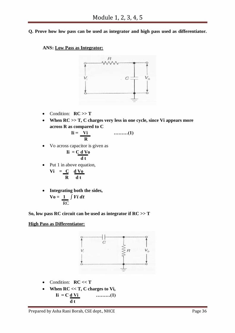
ANS: Low Pass as Integrator:
Condition: RC >> T
When RC >> T, C charges very less in one cycle, since Vi appears more
across R as compared to C
Ii = Vi ………(1)
R
Vo across capacitor is given as
Ii = C d Vo
d t
Put 1 in above equation,
Vi = C d Vo
R d t
Integrating both the sides,
Vo = 1 ∫ 𝑽𝒊 𝒅𝒕
RC
So, low pass RC circuit can be used as integrator if RC >> T
High Pass as Differentiator:
Condition: RC << T
When RC << T, C charges to Vi,
Ii = C d Vi ………(1)
d t

Module 1, 2, 3, 4, 5
Prepared by Asha Rani Borah, CSE dept., NHCE Page 37
Vo across capacitor is given as
Ii = Vo
R
Put 1 in above equation,
Vo = C d Vi
R d t
Vo = RC d Vi
d t
So, high pass RC circuit can be used as differentiator if RC << T
Diode as clipper
Used to clip or remove whole or part input signal
Examples of wave shaping circuits
Also known as non linear circuit, slicers, amplitude selectors
Two types: series and shunt clippers
Series Clipper: (for your reference only, for exam study shunt clippers)
Positive Series clipper:
Diode is series with input signal
During +ve input cycle, D = OFF, so no current in circuit => No output
During -ve input cycle, D = ON, so current in circuit flowing through resistor,
Output voltage α Input voltage
Negative Series clipper:
Diode is series with input signal
During +ve input cycle, D = ON, so current in circuit flowing through resistor,
Output voltage α Input voltage
During -ve input cycle, D = OFF, so no current in circuit => No output

Module 1, 2, 3, 4, 5
Prepared by Asha Rani Borah, CSE dept., NHCE Page 38
Shunt Clippers:
Positive Clipper with Bias
Diode parallel to input signal
During +ve input cycle,
0 <Vin <V => D = OFF, so current in circuit flowing to output,
Output voltage α Input voltage
V <Vin <Vm => D = ON, so current in circuit flowing gnd,
Output = V
During -ve input cycle, D = OFF, so current in circuit flowing to output,
Output voltage α Input voltage
Negative Clipper with Bias
Diode parallel to input signal
During +ve input cycle, D = OFF, so currnt in circuit flowing to output,
Output voltage α Input voltage
During -ve input cycle,
0 <Vin < - V => D = OFF, so current in circuit flowing to output,
Output voltage α Input voltage
- V <Vin < -Vm => D = ON, so current in circuit flowing to gnd,
Output = -V

Module 1, 2, 3, 4, 5
Prepared by Asha Rani Borah, CSE dept., NHCE Page 39
Diode as Clamper
Negative Clamper:
During +ve input cycle, D = ON, so current flows through the diode giving a path for
C to charge. Capacitor charges to positive peak of Input (Vm). The output across
diode is zero.
During -ve input cycle,
D = OFF, so no current through diode. So the Input flows to output. Since
input potential has changed, capacitor starts discharging from (Vm).
Output voltage α Input voltage + voltage discharged by capacitor
Vo= - Vm + ( - Vm) = -2 Vm
During next +ve input cycle, D = ON,
Since RC >>> t of input signal, capacitor will discharge slowly and stay at peak
value for long time.
So, at positive peak of input => output will be 0
At negative peak of input => output is – 2Vm

Module 1, 2, 3, 4, 5
Prepared by Asha Rani Borah, CSE dept., NHCE Page 40
Positive Clamper:
During -ve input cycle, D = ON, so current flows through the diode giving a path for
C to charge. Capacitor charges to negative peak of Input ( -Vm). The output across
diode is zero.
During +ve input cycle,
D = OFF, so no current through diode. So the Input flows to output. Since
input potential has changed, capacitor starts discharging from (Vm).
Output voltage α Input voltage + voltage discharged by capacitor
Vo = Vm + Vm = 2 Vm
During next -ve input cycle, D = ON,
Since RC >>> t of input signal, capacitor will discharge slowly and stay at peak
value for long time.
So, at negative peak of input => output will be 0
At positive peak of input => output is 2Vm
Q. What is Multivibrators? Mention the types of Multivibrators.
Q.Explain the various types of multivibrator. Also mention the applications.
Ans:
A multivibrator is an electronic circuit that switches between two states due to
regenerative feedback. It is used to implement a variety of simple two-state systems such
as oscillators, timers and flip-flops. It is characterized by two amplifying devices cross-
coupled by resistors or capacitors. There are three types of multivibrator circuit depending on
the circuit operation:
ASTABLE, in which the circuit is not stable in either state —it continually
switches from one state to the other. It does not require an external trigger pulse.
Also known as free running multivibrator.
MONOSTABLE, in which one of the states is stable, but the other state is quasi
(unstable). A trigger causes the circuit to enter the quasi state. After entering the
quasi state, the circuit will return to the stable state after a set time. Such a circuit is

Module 1, 2, 3, 4, 5
Prepared by Asha Rani Borah, CSE dept., NHCE Page 41
useful for creating a timing period of fixed duration in response to some external
event. This circuit is also known as a one shot or mono shot.
BISTABLE, in which the circuit has two stable states. The circuit can be flipped
from one state to the other by an external trigger. Also known as flip-flop.
Q. With a circuit diagram, and waveform explain the working of transistor based
Bistable multivibrator circuits.
ANS:
Bistable Multivibrators have TWO stable states and maintain a given output state
indefinitely unless an external trigger is applied.
Switches from one stable state to the other by the application of an external trigger
pulse thus, it requires two external trigger pulses.
Since has two stable states they are more commonly known as Latches and Flip-
flops for use in sequential type circuits.( it "flips" into one logic state, remains there
and then changes or "flops" back into its first original state)
Construction:
Has two NPN transistors Q1 and Q2.
Collector of Q1 coupled to base of Q2 through R1.
Collector of Q2 coupled to base of Q1 through R2.
2. C1 and C2 capacitors are known as speed up capacitors. Their function is to increase the
speed of the circuit in making transition from one stable state to another stable state faster.
The base resistors R3 and R4 of both the transistors are connected to a common source
(-VBB) to ensure one of the transistor remains in cut off region.
Waveform:

Module 1, 2, 3, 4, 5
Prepared by Asha Rani Borah, CSE dept., NHCE Page 42
Uses:
1. In timing circuits as frequency divider
2. In counting circuits
3. In computer memory circuits
Q. Explain the internal block diagram of 555 timer IC.
Ans:
Pin 1: Grounded Terminal: All the voltages are measured with respect to this terminal.
Pin 2: Trigger Terminal: This pin is an inverting input to a comparator that is responsible
for transition of flip-flop from set to reset. The output of the timer depends on the amplitude
of the external trigger pulse applied to this pin. When a negative going pulse of amplitude
greater than 1/3 VCC is applied to this pin, the output of the timer high. The output remains
high as long as the trigger terminal is held at a low voltage.
Pin 3: Output Terminal: Output of the timer is available at this pin.
Pin 4: Reset Terminal: To disable or reset the timer a negative pulse is applied to this pin
due to which it is referred to as reset terminal. When this pin is not to be used for reset
purpose, it should be connected to + VCC.
Pin 5: Control Voltage Terminal: The function of this terminal is to control the threshold
and trigger levels. When this pin is not used, it should be connected to ground through a 0.01
μF capacitor to avoid any noise problem.
Pin 6: Threshold Terminal: This is the non-inverting input terminal of comparator 1, which
compares the voltage applied to the terminal with a reference voltage of 2/3 VCC. When the
voltage at this pin is greater than or equal to the threshold voltage 2/3 VCC, the output of the
timer low.

Module 1, 2, 3, 4, 5
Prepared by Asha Rani Borah, CSE dept., NHCE Page 43
Pin 7: Discharge Terminal: This pin is connected internally to the collector of transistor and
mostly a capacitor is connected between this terminal and ground. It is called discharge
terminal because when transistor saturates, capacitor discharges through the transistor. When
the transistor is cut-off, the capacitor charges at a rate determined by the external resistor and
capacitor.
Pin 8: Supply Terminal: A supply voltage of + 5 V is applied to this terminal with respect
to ground (pin 1).
Q. Discuss briefly the working operation of Astable multivibrator using IC 555 timer.
Q. With neat figure and relevant wave forms explain the operation of astable
multivibrator using IC 555 timer.
Q. With the aid of circuit pin diagram and waveforms, explain the operation of 555
timer as an ASTABLE multi vibrator to get 50% duty cycle.
Ans:

Module 1, 2, 3, 4, 5
Prepared by Asha Rani Borah, CSE dept., NHCE Page 44
Since Q = high, the discharge transistor saturates and pin 7 grounds so that the
capacitor C discharges through resistance RB.
The discharging time constant,
td or TL0W = 0.693 RB C
With the discharging of capacitor, trigger voltage at inverting input of comparator 2
decreases.
When it drops below 1/3VCC, the output of comparator 2 goes high and this reset the
flip-flop, so Q = low and Q = 1.
VOUT = high.
Since Q=0, the discharging transistor is cut-off and the capacitor C begins charging.
Thus the cycle repeats.
Formula derivation:
Voltage across the capacitor at any instant during charging period is given as,

Module 1, 2, 3, 4, 5
Prepared by Asha Rani Borah, CSE dept., NHCE Page 45
VC=VCC(1-et/RC) The time taken by the capacitor to charge from 0 to +1/3 VCC
1/3 VCC = VCC (1-et/RC
)
t1 = 0.405 RC
Similarly, the time taken by the capacitor to charge from 0 to +2/3 VCC
2/3 VCC = VCC (1-et/RC
)
t2 = 1.0986 RC
So the time taken by the capacitor to charge from +1/3 VCC to +2/3 VCC
tC = (t2 – t1) = (10986 – 0.405) RC = 0.693 RC
Since capacitor C charges through resistances RA and RB, the charging time constant is (RA +
RB) C. Substituting R = (RA + RB) in above equation we have
THIGH = tc = 0.693 (RA + RB) C
Voltage across the capacitor at any instant during discharging period is given as
vc = 2/3 VCC e- td/ RBC
The time taken by the capacitor to charge from +2/3 VCC to +1/3 VCC
1/3 VCC = 2/3 VCC e- td/ RBC
td = 0.693 RBC
Overall period of oscillations, T = THIGH + TLOW = 0.693 (RA+ 2RB) C.
The duty cycle, the ratio of the time tc during which the output is high to the total time
period T is given as % duty cycle, D = THIGH / T * 100
NOTE:
From the above equation it is obvious that square wave (50 % duty cycle) output
cannot be obtained.
However, a symmetrical square wave can be obtained if a diode is connected across
resistor RB.
The capacitor C charges through RA and diode D to approximately + 2/3VCC and
discharges through resistor RB and terminal 7 (transistor) until the capacitor voltage
drops to 1/3 VCC. Then the cycle is repeated.
THIGH = 0.693 RA C
TL0W = 0.693 RB C

Module 1, 2, 3, 4, 5
Prepared by Asha Rani Borah, CSE dept., NHCE Page 46
Q. Explain working of Monostable multivibrator using 555 timer IC.
Ans:
Waveforms:

Module 1, 2, 3, 4, 5
Prepared by Asha Rani Borah, CSE dept., NHCE Page 47
Module 3 -: Combinational Logic Circuits
Syllabus : Karnaugh maps, Quine-Mc Clusky method, Half adder, Full adder, Subtractor, Multiplexers and De-multiplexers, Magnitude comparators(1 and 2 bit ), Design of multiple output circuits using PLDs. Introduction to HDL, Verilog Implementation of Data Processing Circuits
Digital Electronics circuits or Logic Circuits are categorized into 2 types: 1. Combinational Logic Circuits: Circuits without memory 2. Sequential Logic Circuits: Circuits with memory
Combinational Logic Circuits The output of combinational logic circuit depends only on the current inputs. There are two fundamental approaches in logic design:
The Sum-of-Products (SOP) – Solution results in an AND -OR or NAND-NAND network
The Product-of-Sums (POS) Method – Solution results in an OR-AND or NOR-NOR network
SOP SUM OF PRODUCTS METHOD
• The fundamental products are also called minterms.
Sum-of-Products (SOP) Equation
The SOP equation can be represented by an expression that is a sum of minterms, where each
minterm is ANDed with the value of Y for the corresponding valuation of input
variables.Consider the following Truth table:
Here, we have to locate output 1 in the truth table and write down the minterm.

Module 1, 2, 3, 4, 5
Prepared by Asha Rani Borah, CSE dept., NHCE Page 48
For instance, the second output 1 appears for an input A=0, B=1. The corresponding
minterm is A'B.
The next output 1 appears for A=1, B=0. The corresponding minterm is AB'.
Y = m1 + m2 + m3
= A’ . B + A . B’ + A . B
Compact form
Y = f(A, B) = Σ m(1, 2, 3)
Logic circuit: using AND –OR gate
Using NAND gate
Example:
Truth table
Y=A'BC+AB'C+ABC'+ABC
Y=F(A,B,C)=∑m(3,5,6,7)

Module 1, 2, 3, 4, 5
Prepared by Asha Rani Borah, CSE dept., NHCE Page 49
POS
PRODUCT OF SUMS METHOD
• Given a truth table, identify the fundamental sums needed for a logic design.
• Then by ANDing these sums, we get the product-of-sums equation corresponding to the
truth table.
• The fundamental sum produces an output 0 for the corresponding input condition.
In POS, each sum term is called maxterm and is designated by M.
Locate each output 0 in the truth table and write down its fundamental sum.
To get the product-of-sums equation, AND the fundamental sums.
Y= (A+B+C)(A+B'+C')(A'+B'+C)
Y= ∏M (0,3,6)
K-MAP (Karnaugh maps)

Module 1, 2, 3, 4, 5
Prepared by Asha Rani Borah, CSE dept., NHCE Page 50
Karnaugh map (K-map) is a visual display of the fundamental products foa a
SOP equation f
Developed by Maurice Karnaugh, an American Physicist KMAP METHOD FOR SIMPLIFYING BOOLEAN EQUATIONS
1. Enter a 1 on map for each fundamental product that produces a 1 output in truth table. Enter 0s elsewhere.
2. Encircle the octets. (Octet is a group of eight 1s. It eliminates three variables and their complements.)
3. Encircle the quads. (A quad is a group of four 1s that are horizontally or Vertically adjacent. It eliminates 2 variables and their complements.) 4. Encircle the pairs.(A pair is a group of two 1s that are horizontally or vertically adjacent. It eliminates one variable and its complement.) 5. If any isolated 1s remain, encircle each.
6. Eliminate any redundant group.
7. Write boolean equation by ORing the products corresponding to the encircled group. This gives SOP terms.
Two variable K Map
Cell numbering K map for the given truth table Y= A Three variables K MAP

Module 1, 2, 3, 4, 5
Prepared by Asha Rani Borah, CSE dept., NHCE Page 51
Y= ∑m (2, 6, 7)
B C BC BC BC
A 0 1 3 2
A 4 5 7 6
Y = AB + BC Four Variables K Map
Y=F(A,B,C,D)=∑m(2,6,7,14)
B C BC BC BC
A 0 0 0 1
A 0 0 1 1
1
1 1 1

Module 1, 2, 3, 4, 5
Prepared by Asha Rani Borah, CSE dept., NHCE Page 52
Y = ABC + BCD + A BCD DON’T CARE CONDITIONS • In some logic circuits, certain input conditions never occur; therefore the corresponding output never appears. • In such cases, the output level is not defined; it can be either HIGH or LOW. These output levels are indicated by'X' in the truth tables and are called don't care conditions
Y= f (A, B, C, D) = ∑ m (9) + dc ( 10, 11, 12, 13, 14, 15)
Y = AC

Module 1, 2, 3, 4, 5
Prepared by Asha Rani Borah, CSE dept., NHCE Page 53
POS Simplification
A B C D Y
0 0 0 0 0
0 0 0 1 1
0 0 1 0 0
0 0 1 1 1
0 1 0 0 0
0 1 0 1 1
0 1 1 0 1
0 1 1 1 1
1 0 0 0 1
1 0 0 1 1
1 0 1 0 0
1 0 1 1 0
1 1 0 0 1
1 1 0 1 1
1 1 1 0 0
1 1 1 1 0
f(A, B, C, D) = πM(0, 2, 4, 10, 11, 14, 15)
C + D C + D C + D C + D
A + B 0 1 3 2
A + B 4 5 7 6
A + B 12 13 15 14
A + B 8 9 11 10

Module 1, 2, 3, 4, 5
Prepared by Asha Rani Borah, CSE dept., NHCE Page 54
Y = (A + B + D) ( A + C + D) ( A + C)
EXAMPLE 1: Y = f(A, B, C) = Σ m (2, 3, 4, 6) = A’BC’ + A’BC + AB’C’ + ABC’
The simplified expression Y = A’B + AC’ EXAMPLE 2: Simplify Y = f(A, B, C) =Σ m (1, 2, 3, 5, 6, 7)

Module 1, 2, 3, 4, 5
Prepared by Asha Rani Borah, CSE dept., NHCE Page 55
The simplified expression Y= B + C.
EXAMPLE 3: Simplify Y = Σ m (0, 1, 2, 4, 5, 6, 8, 9, 10, 12, 13).
The simplified equation is Y = C’ + A’D’ + B’D’.
EXAMPLE 4: Simplify Y = Σ m ( 2, 3, 6, 7, 8, 9) + dc (10, 11, 12, 13, 14, 15)

Module 1, 2, 3, 4, 5
Prepared by Asha Rani Borah, CSE dept., NHCE Page 56
The simplified equation is Y = A + C
Conversion between SOP and POS
SOP and POS occupy complementary locations in a truth table. One representation can be obtained by the other by 1. Identifying complementary locations 2. Changing minterm to maxterm or reverse 3. Changing summation by product or reverse Example:
1. Consider Y = f(A, B, C) = πM(0, 3, 6). The SOP equivalent is Y= Σm(1, 2, 4, 5, 7). 2. Consider Y = f(A, B, C, D) = Σm(0, 3, 5, 6, 12, 14). The SOP equivalent is Y= πM (1, 2, 4, 7, 8, 9, 10, 11, 13, 15). 3. Consider Y = f(A, B, C, D) = Σm (0, 3, 6, 9,11,13,15) + dc (2, 10, 14) The SOP equivalent is Y= πM (1, 4, 5, 7, 8, 12)+ dc (2, 10, 14) LIMITATIONS OF KMAP • The map method depends on the user's ability to identify patterns that gives largest size. • The map method becomes difficult to adapt for simplification of 5 or more variables.
SIMPLIFICATION BY QUINE Mc-CLUSKEY METHOD
• Quine McCluskey method is a systematic approach for logic simplification that does not have the limitations of K Map and also can easily be implemented in a digital computer.
• Quine McCluskey method involves preparation of 2 tables:

Module 1, 2, 3, 4, 5
Prepared by Asha Rani Borah, CSE dept., NHCE Page 57
→ one determines prime implicants and
→ other selects essential prince implicants to get minimal expression.
• Prime implicants are expressions with least number of literals that represents all the terms given in a truth table.
• Prime implicants are examined to get essential prime implicants for a particular expression that avoids any type of duplication.
PROCEDURE USED FOR DETERMINING ESSENTIAL PRIME IMPLICANTS
• In stage 1 of the process, find out all the terms that gives output 1 from truth table and put them in different groups depending on how many 1 input variable combinations have.
For example, first group has no 1 in input combination, second group has only one 1,third two1s,fourth three 1s and fifth four 1s. We also write decimal equivalent of each combination to their right for convenience.
• In stage 2, try to combine first and second group of stage 1,on a member to member basis.
• The rule is to see if only one binary digit is differing between two members and mark that position by '-'. This means corresponding variable is not required to represent those members.
• In stage 3, combine members of different groups of stage 2 in a similar way. Now it will have two '-'elements in each combination. This means each combination requires 2 literals to represent it.
• Repeat stage 4 as stage 3 if required. It will have three '-'elements in each combination. This means each combination requires 1 literal to represent it.
• Next step is to select essential prime implicants and remove redundancy or duplication among them. For this, prepare a table, along with the row lists all the prime implicants and along columns lists all minterms.
• The cross-point of a row and column is ticked if the term is covered by corresponding prime implicants.

Module 1, 2, 3, 4, 5
Prepared by Asha Rani Borah, CSE dept., NHCE Page 58

Module 1, 2, 3, 4, 5
Prepared by Asha Rani Borah, CSE dept., NHCE Page 59
Y=A'B'+B'C+AB'+AC
Y=A'B'+B'C+AB or Y=A'B'+AC+AB
Example 2:
Simplify the following function: Y = f(A, B, C, D) = Σ m(0, 1, 2, 3, 10, 11, 12, 13, 14, 15)

Module 1, 2, 3, 4, 5
Prepared by Asha Rani Borah, CSE dept., NHCE Page 60
Prime implicants: Y = A’B’ + AB + AC + B’ C
Y = A’B’ + AB + AC
Arithmetic Circuits
Half adder:
Addition rules:
1.0+0 = 00 2. 0+1 = 01 3.1+0 = 01 4.1+1 = 10
INPUTS OUTPUTS
A B S CARRY
0 0 0 0
0 1 1 0
1 0 1 0
1 1 0 1
Sum = A B’ + A’ B = A XOR B Carry = AB

Module 1, 2, 3, 4, 5
Prepared by Asha Rani Borah, CSE dept., NHCE Page 61
FULL ADDER:
SUM = A XOR B XOR Cin
Cout = AB + Cin (A XOR B)

Module 1, 2, 3, 4, 5
Prepared by Asha Rani Borah, CSE dept., NHCE Page 62
Half Subtractor:
Subtraction rules:
1.0-0 = 00 2. 0-1 = 11 3.1-0 = 01 4.1-1 = 00
INPUTS OUTPUTS
A B D Borrow
0 0 0 0
0 1 1 1
1 0 1 0
1 1 0 0
Difference = A B’ + A’ B = A XOR B Borrow= AB
FULL SUBTRACTOR:

Module 1, 2, 3, 4, 5
Prepared by Asha Rani Borah, CSE dept., NHCE Page 63
Difference = A XOR B XOR C Bout = AB + C (A X-NOR B)
Parallel Adder Parallel Adder is a digital circuit capable of finding the arithmetic sum of two
binary numbers by operating on corresponding pairs of bits in parallel.
It consists of full adders connected in a chain where the output carry from
each full adder is connected to the carry input of the next higher order full
adder in the chain.

Module 1, 2, 3, 4, 5
Prepared by Asha Rani Borah, CSE dept., NHCE Page 64
A n bit parallel adder requires n full adders to perform the operation.
The given figure is 4 bit parallel adder
Working of parallel Adder –
1. As shown in the figure, firstly the full adder FA0 adds A0 and B0 along with the carry C0 to generate the sum S0 (the first bit of the output sum) and the carry C1 which is connected to the next adder in chain.
2. Next, the full adder FA1 uses this carry bit C1 to add with the input bits A1 and B1 to generate the sum S1(the second bit of the output sum) and the carry C2 which is again further connected to the next adder in chain and so on.
3. The process continues till the last full adder.
Parallel Adder/Subtractor
The addition and subtraction operations can be done using an Adder-Subtractor circuit. The figure shows the logic diagram of a 4-bit Adder-Subtractor circuit.
When M = 0, the output of XOR gate will be Bi ⊕ 0 = B
i.
If the full adders receive the value of B, and the input carry C0
is 0, the circuit
performs A plus B.
When M = 1, the output of XOR gate will be Bi ⊕ 1 = B
i
’
.
If the full adders receive the value of B’, and the input carry C0 is 1, the circuit
performs A plus 1’s complement of B plus 1, which is equal to A minus B.

Module 1, 2, 3, 4, 5
Prepared by Asha Rani Borah, CSE dept., NHCE Page 65
DATA PROCESSING CIRCUITS
Data-processing circuits are logic circuits that process binary data. Such circuits may be multiplexers, demultiplexer, encoder, decoder.
Multiplexer
Multiplex means many into one.
In digital computer networks, multiplexing is a method by which multiple digital data streams are combined into one signal over a shared medium.
A digital circuit that performs the multiplexing of digital signals is called a multiplexer (or MUX in short).
Multiplexer is a combinational logic circuit that can select one of many inputs.
Multiplexer is also called a data selector.
General multiplexer block diagram
4:1 MUX
Selection Lines Output

Module 1, 2, 3, 4, 5
Prepared by Asha Rani Borah, CSE dept., NHCE Page 66
Y = S1’ S0’D0 + S1’ S0 D1 + S1 S0’D2 + S1 S0 D
Multiplexer Logic
Multiplexer can be used to realize a given Boolean equation. Multiplexer is called universal logic circuit because a 2n-to-1 multiplexer can be used to design solution for any n-variable truth table.
S1 S0 Y
0 0 D0
0 1 D1
1 0 D2
1 1 D3

Module 1, 2, 3, 4, 5
Prepared by Asha Rani Borah, CSE dept., NHCE Page 67
Y = ∑ m ( 0, 2, 3, 4, 5, 8, 9, 10, 11, 12, 13, 14, 15)
Multiplexer Trees Design a 4-to-1 multiplexer 2 to 1 multiplexer.
8:1
MUX

Module 1, 2, 3, 4, 5
Prepared by Asha Rani Borah, CSE dept., NHCE Page 68
Solve:Design a 32-to-1 multiplexer using two 16:1 and one 2:1 MUX. DEMULTIPLEXER
Demultiplex means one into many.
It is a digital circuit with 1 input and many outputs
By applying control signals, the input signal is send to one of the output lines.
1-to-2 Demultiplexer

Module 1, 2, 3, 4, 5
Prepared by Asha Rani Borah, CSE dept., NHCE Page 69
Y0 = D A’ , Y1 = D A
De-multiplexer Tree Design 1:32 De-Mux using 1:16 De-Mux.
De-Mux application:

Module 1, 2, 3, 4, 5
Prepared by Asha Rani Borah, CSE dept., NHCE Page 70
Q) Implement a full adder using a 1 to 8 demux.
Truth table for full adder
A B C Sum Carry
0 0 0 0 0
0 0 1 1 0
0 1 0 1 0
0 1 1 0 1
1 0 0 1 0
1 0 1 0 1
1 1 0 0 1
1 1 1 1 1
MAGNITUDE COMPARATOR • It compares two n-bit binary numbers, say X and Y and activates one of these 3 outputs: X=Y, >Yand X<Y • The logic equations for the outputs can be written as follows, where G, L, E stand for greater than, less than andequal to respectively.
(X>Y): G=XY' (X<Y): L=X'Y (X=Y): E=X'Y'+XY =(XY'+X'Y)'=(G+L)'

Module 1, 2, 3, 4, 5
Prepared by Asha Rani Borah, CSE dept., NHCE Page 71
1-bit Magnitude Comparator
INPUTS OUTPUTS
X Y X >Y X=Y X< Y
0 0 0 1 0
0 1 0 0 1
1 0 1 0 0
1 1 0 1 0
Design two bit magnitude comparator. (solve)
n- bit magnitude comparator: For a 2-bit magnitude comparator:

Module 1, 2, 3, 4, 5
Prepared by Asha Rani Borah, CSE dept., NHCE Page 72
Similarly, for n-bit magnitude comparator will be:
Programmable Array Logic(PAL) This is a programmable array of logic gates on a single chip.
This is different from a PROM because it has a programmable AND array and a fixed OR array.
With a PROM programmer, we can burn in the desired fundamental products, which are then ORed by the fixedoutput connections.

Module 1, 2, 3, 4, 5
Prepared by Asha Rani Borah, CSE dept., NHCE Page 73
Realize a full adder using PAL
S = Σ m(1, 2, 4, 7) Co = Σ m(3, 5, 6, 7)

Module 1, 2, 3, 4, 5
Prepared by Asha Rani Borah, CSE dept., NHCE Page 74
PROGRAMMABLE LOGIC ARRAYS (PLA)
In this, the input signals are presented to an array of AND gates while the outputs are taken from an array of OR gates.
In a PROM, the input AND gate array is fixed and cannot be altered, while the output OR gate array is fusible linked, and can thus be programmed.
In PAL, the output OR gate array is fixed while the input AND gate array is fusible linked and thus programmable.
The PLA is much more versatile than the PROM or the PAL, since both its AND gate array and its OR gate are fusible linked and programmable.
PLA is also more complicated to utilize since the number of fusible links are doubled.
1.Show how we can program a PLA. f(a,b,c) = a’b’ + abc g(a,b,c) = a’b’c’ + ab + bc h(a,b,c) = c

Module 1, 2, 3, 4, 5
Prepared by Asha Rani Borah, CSE dept., NHCE Page 75
2. Realise BCD to seven segment display using PLA.

Module 1, 2, 3, 4, 5
Prepared by Asha Rani Borah, CSE dept., NHCE Page 76
Module 4 -: Sequential Circuit Elements Syllabus: Latches, types of Flip-flops, Flip-flop excitation tables, Registers, type of Shift Registers, Universal shift Registers, Applications of Shift Registers –Ring Counter, Johnson Counter, Sequence generator, Verilog implementation of Flip-flops and Registers. Comparison between combinational and sequential logic circuits
Combinational circuits Sequential circuits
1. The output variables depends upon on the
combination of inputs variables
The output variables depends upon on the
present inputs variables and also on
previous history of these input variables.
2. Memory unit not required Memory unit is required to store the past
history of input variables
3. It does not require any feedback. It simply
outputs the input according to the logic
designed.
It involves feedback from output to input
that is stored in the memory for the next
operation.
4. Faster in speed because the delay in only
due to propagation delay of gates used
between input and output stages.
Slower in speed as delay is because of
propagation delay and also due to input
dependent on previous output.
5. Easy to design Complex than combinational to design
6. Logic gates are building block Flip Flops are building blocks
7. No clock required Clock required of operation
8. Used mainly for Arithmetic and Boolean
operations.
Used for storing data
9. e.g. parallel adder, decoder, MUX e.g. Serial adder, flip flops, counters
Latch:
SR NOR gate latch
R(reset) and S(set) are the inputs.
Q and Q’ are the outputs where Q’ is complement of Q always
(NOTE: for ur reference only, NOR gate truth table)

Module 1, 2, 3, 4, 5
Prepared by Asha Rani Borah, CSE dept., NHCE Page 77
A B Y
0 0 1
0 1 0
1 0 0
1 1 0
Working:
1. R=S=0,
Assuming previous Q=0, Q’=1,
first NOR gate, input R=0, Q’ =1 => output Q =0
second NOR gate, input S=0, Q =0 => output Q’=1
Assuming previous Q=1, Q’=0, NO change in state
first NOR gate, input R=0, Q’ =0 => output Q = 1
second NOR gate, input S=0, Q =1 => output Q’=0
2. R=0, S=1,
Since, Second NOR gate, input S=1 => output Q’=0
First NOR gate, input R=0, Q’ =0 => output Q =1 Q=1, Q’= 0
Set condition
3. R=1, S=0,
Since, first NOR gate, input R=1 => output Q =0
second NOR gate, input S=0, Q =0 => output Q’=1 Q=0, Q’= 1
Reset condition
4. R=S=1,
Assuming previous Q=0, Q’=1,
first NOR gate, input R=1, Q’ =1 => output Q =0
second NOR gate, input S=1, Q =0 => output Q’=0
both Q = Q’=0 not possible
Assuming previous Q=1, Q’=0,
first NOR gate, input R=1, Q’ =0 => output Q = 0 Illegal or forbidden state
second NOR gate, input S=1, Q =1 => output Q’=0
Flip flop:
A flip-flop is a bistable electronic circuit that has two stable states. The first electronic flip-
flop was invented by British physicists William Eccles and F. W. Jordan in 1918. It was
initially called the Eccles- Jordan trigger circuit.
Types: SR, JK, D, T
Clocked SR Flip flop

Module 1, 2, 3, 4, 5
Prepared by Asha Rani Borah, CSE dept., NHCE Page 78
Construction:
Two NAND gate added to inputs R & S to make RS latch as Flip flop.
Clock is added as input to enable or disable the latch.
Clock can be level or edge triggered
Working:
1. Clk =1, R=S=0,
Since Clk =1, Both Input NAND gate output depends upon S & R inputs
Assuming previous Q=0, Q’=1,
input S=0, X=1, Q’ =1 => output Q =0
input R=0, Y=1, Q =0 => output Q’=1
Assuming previous Q=1, Q’=0, NO change in state
input S=0, X=1, Q’ =0 => output Q =1
input R=0, Y=1, Q =1 => output Q’=0
2. Clk = 1, S=0, R=1,
Since Clk =1, Both Input NAND gate output depends upon S & R inputs
Since, input R=1, Y=0 => output Q’=1
input S=0, X=1,Q’ =1 => output Q =0 Q=0, Q’= 1
Reset condition
3. Clk =1, S=1, R=0,

Module 1, 2, 3, 4, 5
Prepared by Asha Rani Borah, CSE dept., NHCE Page 79
Since Clk =1, Both Input NAND gate output depends upon S & R inputs
Since, input S=1, X=0 => output Q =1
input R=0, Y=1, Q =1 => output Q’ =0 Q=1, Q’= 0
Set condition
4. Clk = 1, S=R=1,
Assuming previous Q=0, Q’=1,
inputS=1, X= 0, Q’ =1 => output Q =1
input R=1, Y=0, Q =0 => output Q’=1 both Q = Q’=1 not possible
Assuming previous Q=1, Q’=0,
inputS=1, X=0, Q’ =0 => output Q = 1 Illegal or forbidden state
input R=1, Y=0, Q =1 => output Q’=1
5. Clk = 0,
Since Clk =0, Both Input NAND gate output = 0
Input S & R has no control on the latch => S =R =don’t care
Since X=Y=0, SR latch stays in NO change condition
(NOTE: for ur reference only, NAND gate truth table)
A B Y
0 0 1
0 1 1
1 0 1
1 1 0
Excitation Table of SR flip flop
Qn Qn+1 S R
0 0 0 X
0 1 1 0
1 0 0 1
1 1 X 0
Characteristics Equation

Module 1, 2, 3, 4, 5
Prepared by Asha Rani Borah, CSE dept., NHCE Page 80
S R Qn Qn+1
0 0 0 0
0 0 1 1
0 1 0 0
0 1 1 0
1 0 0 1
1 0 1 1
1 1 0 X
1 1 1 X SR FLIP FLOP TRUTH TABLE
K MAP OF Qn+1
Qn+1 =S+RQn
Edge Triggered JK flip flop
Construction:
To avoid the forbidden state of the SR flip flop =>Two AND gate added to inputs SR
Flip flop => this makes JK flip flop
Enable is connected to positive edge triggered clock. Enable can be connected to
negative edge triggered clock also.
Working:
1. At positive edge triggered, J=K=0,
Both Input AND gate output depends upon J&K inputs

Module 1, 2, 3, 4, 5
Prepared by Asha Rani Borah, CSE dept., NHCE Page 81
input J=0, AND gate output =>S=0
input K=0, AND gate output =>R=0
Since S=0, R =0, according to SR flip flop=>NO change in state
2.At positive edge triggered, J=0, K=1,
Both Input AND gate output depends upon J & K inputs
Assuming previous Q=0, Q’=1,
input J=0& Q’=1,AND gate output => S=0 Q=0, Q’=1
input K=1& Q=0, AND gate output => R=0
Q =0, Q’ =1
Assuming previous Q=1, Q’=0, Reset condition
input J=0 & Q’= 0, AND gate output => S=0 Q=0, Q’=1
input K=1 & Q=1, AND gate output => R=1
3. At positive edge triggered, J=1, K=0,
Both Input AND gate output depends upon J & K inputs
Assuming previous Q=0, Q’=1,
input J=1 & Q’=1, AND gate output => S=1 Q=1, Q’=0
input K=0 & Q=0, AND gate output => R=0
Q =1, Q’ =0
Assuming previous Q=1, Q’=0, Set condition
input J=1 & Q’= 0, AND gate output => S=0 Q=1, Q’=0
input K=0 & Q=1, AND gate output => R=0
4. At positive edge triggered, J=1, K=1,
Both Input AND gate output depends upon J & K inputs
Assuming previous Q=0, Q’=1,
input J=1 & Q’=1, AND gate output => S=1 Q=1, Q’=0
input K=1 & Q=0, AND gate output => R=0
Q = Q’
Assuming previous Q=1, Q’=0, Toggle condition
input J=1 & Q’= 0, AND gate output => S=0 Q=0, Q’=1
input K=1 & Q=1, AND gate output => R=1
Excitation Table:
Qn Qn+1 J K

Module 1, 2, 3, 4, 5
Prepared by Asha Rani Borah, CSE dept., NHCE Page 82
0 0 0 X
0 1 1 X
1 0 X 1
1 1 X 0
Characteristics Equation
J K Qn Qn+1
0 0 0 0
0 0 1 1
0 1 0 0
0 1 1 0
1 0 0 1
1 0 1 1
1 1 0 1
1 1 1 0 JK FLIP FLOP TRUTH TABLE
K MAP OF Qn+1
Qn+1 = JQn + KQn
Edge triggered D flip flop

Module 1, 2, 3, 4, 5
Prepared by Asha Rani Borah, CSE dept., NHCE Page 83
Construction:
NOT gate added from J to K input.
Enable is connected to positive edge triggered clock.
Enable can be connected to negative edge triggered clock also.
Working:
1. At positive edge triggered, D=0,
Since D=0,
J=0 and K =1=> Reset state of JK flip flop =>Q= 0, Q’ = 1
2.At positive edge triggered, D=1,
Since D=1,
J=1 and K =0=> Set state of JK flip flop =>Q= 1, Q’ = 0
3. No positive trigger, flip flop is disabled, Output remains as previous state
Excitation Table:
Qn Qn+1 D
0 0 0
0 1 1
1 0 0
1 1 1
Characteristics Equation

Module 1, 2, 3, 4, 5
Prepared by Asha Rani Borah, CSE dept., NHCE Page 84
D Qn Qn+1
0 0 0
0 1 0
1 0 1
1 1 1 D FLIP FLOP TRUTH TABLE
K MAP OF Qn+1
Qn+1 = D
Edge triggered T flip flop
Construction:
J connected to K input.
Clock
T
Q(n+1)
0 X Qn
0 Qn
1 Qn

Module 1, 2, 3, 4, 5
Prepared by Asha Rani Borah, CSE dept., NHCE Page 85
Enable is connected to positive edge triggered clock. Enable can be connected to
negative edge triggered clock also.
Working: 1. At positive edge triggered, T=0,
Since T=0,
J=0 and K =0=>No change state of JK flip flop =>Q= Q, Q’=Q’
2. At positive edge triggered, T=1,
Since T=1,
J=1 and K =1=>Toggle state of JK flip flop =>Q= Q’
3. No positive trigger, flip flop is disabled, Output remains as previous state
Excitation Table:
Qn Qn+1 T
0 0 0
0 1 1
1 0 1
1 1 0
Characteristics Equation
T Qn Qn+1
0 0 0
0 1 1
1 0 1
1 1 0 T FLIP FLOP TRUTH TABLE
K MAP OF Qn+1
T’ T
Qn’ 0 1
Qn 1 0
Qn+1 = Qn T + Qn T= T XOR Qn
Racing Problem in JK Flip Flop

Module 1, 2, 3, 4, 5
Prepared by Asha Rani Borah, CSE dept., NHCE Page 86
Consider the JK flip flop diagram, when clock is high and J&K=11 then two upper
and lower AND gates are only triggered by the complementary outputs Q and Q’.
In this condition, according to the propagation delay one gate will be enabled and
another gate is disabled.
If upper gate is disabled then it sets the output and in the next lower gate will be
enabled which resets the flip flop output.
This condition is called race around condition.
Steps to avoid racing condition in JK Flip flop:
1. If the clock high level time is less than the propagation delay of the flip flop then
racing can be avoided. This is done by using edge triggering rather than level
triggering.
2. If the flip flop is made to toggle over one clock period then racing can be avoided. This
is done by Master Slave JK flip flop.
Master Slave J K Flip flop
Master-slave flip flop is designed using two separate flip flops. Out of these, one acts
as the master and the other as a slave.
The output of the master J-K flip flop is fed to the input of the slave J-K flip flop.
The output of the slave J-K flip flop is given as a feedback to the input of the master
J-K flip flop.
The clock pulse [Clk] is given to the master J-K flip flop and it is sent through a NOT
Gate and thus inverted before passing it to the slave J-K flip flop.
Working:
When Clk is positive edge, the master J-K flip flop gets enabled and Slave is disabled.
When Clk is negative edge, Master is disabled.
As Slave is enabled at negative edge. the output of Master reaches to the slave.
So the next Slave output as input to the Master reaches only at next positive edge.
The output changes only after one full cycle which eliminates race around condition.
Conversion of flip flops

Module 1, 2, 3, 4, 5
Prepared by Asha Rani Borah, CSE dept., NHCE Page 87
1. SR Flip Flop to D Flip Flop
Input Preset
State
Next State Flip Flop Inputs
D Qn Qn+1 S R
0 0 0 0 X
0 1 0 0 1
1 0 1 1 0
1 1 1 X 0
. SR Flip Flop to JK Flip Flop
Input Preset Next State Flip Flop Inputs

Module 1, 2, 3, 4, 5
Prepared by Asha Rani Borah, CSE dept., NHCE Page 88
State
J K Qn Qn+1 S R
0 0 0 0 0 X
0 0 1 1 X 0
0 1 0 0 0 X
0 1 1 0 0 1
1 0 0 1 1 0
1 0 1 1 X 0
1 1 0 1 1 0
1 1 1 0 0 1
JK Flip Flop to T Flip Flop
Input Preset
State
Next State Flip Flop Inputs

Module 1, 2, 3, 4, 5
Prepared by Asha Rani Borah, CSE dept., NHCE Page 89
T Qn Qn+1 J K
0 0 0 0 X
0 1 1 X 0
1 0 1 1 X
1 1 0 X 1
D Flip Flop to SR Flip Flop
Input Preset
State
Next State Flip Flop
Input
S R Qn Qn+1 D
0 0 0 0 0
0 0 1 1 1

Module 1, 2, 3, 4, 5
Prepared by Asha Rani Borah, CSE dept., NHCE Page 90
0 1 0 0 0
0 1 1 0 0
1 0 0 1 1
1 0 1 1 1
1 1 0 X X
1 1 1 X X
T Flip Flop to JKFlip Flop
Input Preset
State
Next State Flip Flop
Input
J K Qn Qn+1 T
0 0 0 0 0
0 0 1 1 0

Module 1, 2, 3, 4, 5
Prepared by Asha Rani Borah, CSE dept., NHCE Page 91
0 1 0 0 0
0 1 1 0 1
1 0 0 1 1
1 0 1 1 0
1 1 0 1 1
1 1 1 0 1
K – map simplification
T = J Qn’ + K Qn
REGISTERS • A register is a group of flip-flops used to momentarily store binary-information.
• Each flip-flop can store either 0 or 1.
• The flip-flops used to construct registers are usually edge-triggered JK, SR or D types.
• The register can also be used
→ to accept input-data from an alphanumeric keyboard and then present this data at the
input of a microprocessor-chip.
→ to momentarily store binary-data at the output of a decoder.
→ to perform various arithmetic operations. For ex: multiplication & division.
→ to count number of pulses entering into a system as up-counter, down-counter, ring-
counter or Johnson-counter.
→ as serial-adder, sequence-generator and sequence-detector.
TYPES OF REGISTERS

Module 1, 2, 3, 4, 5
Prepared by Asha Rani Borah, CSE dept., NHCE Page 92
• Shift-register is a group of flip-flops connected in such a way that a binary-number can be
shifted into or out of the flip-flops.
• The bits in a binary-number can be moved from one place to another in following 2 ways:
1. Serial shifting: Data-bits are shifted one after the other in a serial fashion with one bit
shifted at each clock transition
2. Parallel shifting: Data-bits are shifted simultaneously with a single clock transition.
SHIFTING SERIAL BINARY-DATA INTO THE REGISTER
A common clock provides trigger at its negative edge to all the flip-flops
The output of one D flip-flop is connected to input of the next.
At every clock trigger, data stored in one flip-flop is transferred to the next flip-flop.
Serial input ->d input -> Q -> R -> S->T
Let the input be 0100
At clock A, d input =0 , QRST = 0000
At clock B, d input=0, QRST=0000.
At clock C, d input=1, QRST=1000.
At clock D, d input=0, QRST=0100.
SHIFTING BINARY-DATA OUT SERIALLY OF THE REGISTER
Before Time A: The register holds QRST=1010
At Time A: QRST=0101 and serial output =0
At Time B: QRST=0010 and serial output =1
At Time C: QRST=0001 and serial output =0

Module 1, 2, 3, 4, 5
Prepared by Asha Rani Borah, CSE dept., NHCE Page 93
At Time D: QRST=0000and serial output =1.
Thus, the binary-data stored is shifted out of the right-end of the register in a serial
fashion and lost after 4 clock cycles.
Types of shift registers
→ Serial in-Serial out - SISO
→ Serial in-Parallel out - SIPO
→ Parallel in-Serial out - PISO
→ Parallel in-Parallel out – PIPO
1. SISO- SERIAL IN SERIAL OUT
In this shift register, when the clock signal is applied and the serial data is given; only
one bit will be available at output at a time in the order of the input data.
The use of SISO shift register is to act as temporary data storage device.
The main use of a SISO is to act as a delay element.
CLK Serial
Input
Q3 Q2 Q1 Q0 Serial
Output
0 0 0 0 0 0
1 1 0 0 0 0
2 0 1 0 0 0
3 1 0 1 0 0
4 1 0 1 0
5 0 1 0 1 0
6 0 0 1 0 1
7 0 0 0 1 0
8 0 0 0 0 1
2.PIPO – PARALLEL INPUT PARALLEL OUTPUT

Module 1, 2, 3, 4, 5
Prepared by Asha Rani Borah, CSE dept., NHCE Page 94
There are no interconnections between any of the four flip flops.
In one clock, parallel data goes in and parallel output is out.
A Parallel in Parallel out (PIPO) shift register is used as a temporary storage device
and also as a delay element similar to a SISO shift register.
CLK Parallel
Input
Q3 Q2 Q1 Q0
0 0 1 0 1 0 0 0 0
1 0 1 0 1
Parallel output
3. SIPO- SERIAL INPUT PARALLEL OUTPUT
The output of Serial in Parallel out (SIPO) shift register is collected at each flip flop.
The main application of Serial in Parallel out shift register is to convert serial data
into parallel data. Hence they are used in communication lines where demultiplexing
of a data line into several parallel line is required.
CLK Serial
Input
Q3 Q2 Q1 Q0 Serial
Output
0 0 0 0 0 0

Module 1, 2, 3, 4, 5
Prepared by Asha Rani Borah, CSE dept., NHCE Page 95
1 1 0 0 0 0
2 0 1 0 0 0
3 1 0 1 0 0
4 1 0 1 0
Parallel output
4. PISO- PARALLEL INPUT SERIAL OUTPUT
The output of the previous flip flop and parallel data input are connected to the input
of the MUX and the output of MUX is connected to the next flip flop.
A Parallel in Serial out (PISO) shift register converts parallel data to serial data.
Hence they are used in communication lines where a number of data lines are
multiplexed into single serial data line.
CLK Parallel
Input
Q3 Q2 Q1 Q0 Serial
Output
0 0 1 0 1 0 0 0 0
1 0 1 0 1
2 0 0 1 0 1
3 0 0 0 1 0
4 0 0 0 0 1
5 0 0 0 0 0

Module 1, 2, 3, 4, 5
Prepared by Asha Rani Borah, CSE dept., NHCE Page 96
For parallel input, Shift/ load’ input = LOW
This makes G2,G4,G6 AND active, inputs A B C D enters the registers parallel
For serial shifting, Shift/ load’ input = HIGH
This makes G1, G3, G5 AND active, output previous Q enters next stage D input
allowing serial shifting.
Bidirectional shift register
A bidirectional, or reversible, shift register is one in which the data can
be shift either left or right.
For right shift, control line right/ left’ = High
G1, G3, G5, G7 AND gates are active
Serial input (right) -> D3, Q3 -> D2, Q2 -> D1,Q1 -> D0
Serial output available at Q0
For left shift, control line right/ left’ = LOW
G2, G4, G6, G8 AND gates are active
Serial input (left) -> D0, Q0 -> D1, Q1 -> D2, Q2 -> D3
Serial output available at Q3

Module 1, 2, 3, 4, 5
Prepared by Asha Rani Borah, CSE dept., NHCE Page 97
Universal shift register
Can perform SISO, SIPO, PIPO, PISO
Also can do right and left shift
MUX control the operation depending upon S0,S1
When S1 S0 = 01, Right shift
Serial input (right) -> D3, A3-> D2, A2 ->D1, A2 -> D0
(Indicated by green lines)
When S1 S0 = 10, Left shift
Serial input (left) -> D0, A0-> D1, A1 ->D2, A2 -> D3
(indicated by blue lines)
When S1 S0 = 11, parallel loading
Parallel inputs, I0 loads as A0, I1 loads as A1, I2 loads as A1, I3
loads as A3
(Indicated by orange lines)
When S1 S0 = 00, holding or locking data
Previous state output is feedback as input to get same output
A0 fed back to D0, A1 fed back to D1,A2 fed back to D2,A3 fed
back to D3
(Indicated by Red lines)

Module 1, 2, 3, 4, 5
Prepared by Asha Rani Borah, CSE dept., NHCE Page 98
APPLICATIONS OF SHIFT REGISTER
1. RING COUNTER It is a basic shift registers with direct feedback such that the contents of the register
simply circulate around the register when the clock is running.
The output of the most significant stage is fed back to the input of the least significant
stage.
The following is a 4-bit ring counter constructed from D flip-flops. The output of each
stage is shifted into the next stage on the positive edge of a clock pulse.
If the CLEAR signal is high, all the flip flops except the first one FF0 are reset to 0.
FF0 is preset to 1 instead.

Module 1, 2, 3, 4, 5
Prepared by Asha Rani Borah, CSE dept., NHCE Page 99
2. Johnson Counters
Johnson counters are a variation of standard ring counters, with the inverted output of
the last stage fed back to the input of the first stage.
They are also known as twisted ring counters or switched tail counter.
An n-stage Johnson counter yields a count sequence of length 2n, so it may be
considered to be a mod-2n counter.

Module 1, 2, 3, 4, 5
Prepared by Asha Rani Borah, CSE dept., NHCE Page 100
SEQUENCE GENERATOR
• This is used to generate a prescribed-sequence repetitively.
• Shift register can be represented as pipe full of data and each flip-flop represents one
compartment of it.
• The leftmost flip-flop is connected to serial data-in and rightmost provides serial data-out.
• When clock trigger occurs, data-transfer takes place.
• The shift-register is connected like a ring-counter and with triggering of clock; the binary-
word stored in the register comes out sequentially from serial out but does not get lost as it is
fed back as serial-in to fill the register.

Module 1, 2, 3, 4, 5
Prepared by Asha Rani Borah, CSE dept., NHCE Page 101
Module 5 -: Analysis of Sequential Circuit Syllabus: Counters-Asynchronous and synchronous, Design of counters, Counter Design as synthesis problem, Design of Synchronous Sequential Circuits: Moore model, Mealy model, State Reduction Techniques, Verilog implementation of counters.
Counter:
• This is a digital-circuit designed → to keep track of a number of events or → to count number of clock cycles (Figure 1.21). • This can be constructed using → number of flip-flops (e.g. JK, SR, D and T) & → additional electronic circuits. • This is similar to a register, since it is also capable of storing a binary number (e.g. 1011). • The input to the counter is rectangular waveform CLOCK. • Each time the clock signal changes state from low to high (0->1), the counter will add one (1) to the number stored in its flip-flops. In other words, the counter will count the number of clock-transitions from low to high. Types of counters: 1) Asynchronous Counter (Serial Counter)
Each flip-flop is driven by the output of the previous flip-flop i.e. the output of a flip-flop isused as the clock-input for the next flip-flop
Advantage: It requires less hardware.
Disadvantage: It operates at low speed. 2) Synchronous Counter (Parallel Counter)
All flip-flops change states simultaneously since all clock inputs are driven by the same clock.i.e. all the flip-flops change states in synchronism.
Advantage: It operates at high speed.
Disadvantage: It requires more hardware. Counters can also be classified as: 1) Up Counter
It can be used to count upward from a 0 to maximum-count 0 ->1 ->2 ->3 -> 4(MOD-5)
With each clock-transition, the content of the counter is increased by 1. 2) Down Counter:
It can be used to count downward from a maximum-count to 0. 3 ->2 ->1->0.(MOD-4)
With each clock-transition, the content of the counter is decreased by 1. 3) Up-down Counter:
It is capable of counting in either an upward or a downward direction.
Mod 4 = COUNT 0 TO 3 (11 in binary)=> requires 22 => 2 flip flop
Mod 8 = COUNT 0 TO 7(111 in binary) => requires 23=> 3 flip flop

Module 1, 2, 3, 4, 5
Prepared by Asha Rani Borah, CSE dept., NHCE Page 102
Mod 14 = COUNT 0 TO 13(1101 in binary)=> requires 24=> 4 flip flop
Mod 128 = COUNT 0 TO 127(111 1111 in binary) => requires 27 => 7 flip flop
Q1. Explain a 3-bit binary Ripple UP counter. Also write the block diagram,
truth table and waveform.
ANS:
ASYNCHRONOUS 3-BIT UP-COUNTER (RIPPLE-COUNTER)
• Each flip-flop is driven by the output of the previous flip-flop i.e. the output of a flip-flop is used as the clock-input for the next flip-flop. Up-Counter:
It can be used to count upward from a 0 to maximum-count. i.e. it counts in an upward direction. 0 ->1 ->2 ->3->4->5->6->7
With each clock-transition, the content of the counter is increased by 1.
A 3-bit counter can be used to count a maximum of 7 clock-transitions
This can be constructed using clocked JK flip-flops.
All J and K inputs of flip-flops are tied to +Vcc. This means, with each clock-transition, the flip-flop will change its state (toggle
Working:
The counter outputs are A, B, and C.
The system-clock is used to drive(or trigger) flip-flop A.
The output of flip-flop A is used to drive flip-flop B.
Likewise, the output of flip-flop B is used to drive flip-flop C.
The triggers move through flip-flops like a ripple in water. Hence, it is called ripple counter.
Flip-flop A toggles with each clock-transition.
Flip-flop B will toggle each time A goes LOW (1 to 0).
Likewise, flip-flop C will toggle each time B goes LOW (1 to 0).
The overall propagation delay time is the sum of the individual delays.

Module 1, 2, 3, 4, 5
Prepared by Asha Rani Borah, CSE dept., NHCE Page 103

Module 1, 2, 3, 4, 5
Prepared by Asha Rani Borah, CSE dept., NHCE Page 104
Q2) Explain a 3-bit binary Ripple Down counter. Also write the block diagram,
truth table and waveform.
ASYNCHRONOUS 3-BIT DOWN-COUNTER
Each flip-flop is driven by the output of the previous flip-flop i.e. the output of a flip-flop is used as the clock-input for the next flip-flop.
Down Counter:
It can be used to count downward from a maximum-count to 0 it counts in an downward direction ( 7->6->5->4-> 3 ->2 ->1-> 0).
With each clock-transition, the content of the counter is decreased by 1.
A 3-bit counter can be used to count a maximum of 7 clock-transitions.
This can be constructed using clocked JK flip-flops.
All J and K inputs of flip-flops are tied to +Vcc. This means, with each clock-transition, the flip-flop will change its state (toggle).
Working:
The counter outputs are A, B, and C.
The system-clock is used to drive(or trigger) flip-flop A.,
But, the complement of A (i.e. A') is used to drive flip-flop B,
Likewise B' is used to drive flip-flop C.
The triggers move through flip-flops like a ripple in water. Hence, it is called ripple counter.
Flip-flop A toggles with each clock-transition.
But flip-flop B will toggle each time A goes HIGH (0 to 1).
Likewise, flip-flop C will toggle each time B goes HIGH (0 to 1).
The overall propagation delay time is the sum of the individual delays.

Module 1, 2, 3, 4, 5
Prepared by Asha Rani Borah, CSE dept., NHCE Page 105
Q3. Explain a 3-bit binary Ripple Up-down counter. Also write the
block diagram, truth table and waveform.
ASYNCHRONOUS 3-BIT UP-DOWN-COUNTER
Up-down Counter:
It is capable of counting in either an upward or a downward direction.
It is simply a combination of the up counter & down counter.
A 3-bit counter can be used to count a maximum of 7 clock-transitions.
This can be constructed using clocked JK flip-flops.
All J and K inputs of flip-flops are tied to +Vcc. This means, with each clock-transition, the flip-flop will change its state (toggle).
Working: 1) To operate in the Count-up Mode

Module 1, 2, 3, 4, 5
Prepared by Asha Rani Borah, CSE dept., NHCE Page 106
If Count-up = high and the Count-down = low, the lower AND gates Y1 and Y2 are disabled.
The clock applied to flip-flop A will be steered into the other flip-flops by AND gates X1 and X2.
2) To operate in the Count-down Mode
If Count-up = low and the Count-down =high, the upper AND gates X1 and X2 are disabled.
The clock applied to flip-flop A will be steered into the other flip-
flops by AND gates Y1 and Y2. Drawbacks: The additional gates (AND & OR) introduce additional
delays.
Q4. Differentiate synchronous and asynchronous counter.
Asynchronous Counter Synchronous Counter
1. Flip flops are connected such that output of first drives the clock for the next flip flop
No connection between output from first to next flip flop clock.
2. All flip flops are not clocked simultaneously
All the flip flops are clocked simultaneously
3. Simple logic circuit Complex logic circuit
4. Propagation delay is more as clock is propagated through number of flip flops
No propagation delay as simultaneous clock given to all flip flops
5 Difficult to design Can be designed
Q 5) Explain a 3-bit binary synchronous up counter. Also write the block
diagram, truth table and waveform.

Module 1, 2, 3, 4, 5
Prepared by Asha Rani Borah, CSE dept., NHCE Page 107
SYNCHRONOUS 3 BIT UP-COUNTER (PARALLEL BINARY COUNTER)
All flip-flops change states simultaneously since all clock inputs are driven by the same clock i.e. all the flip-flops change states in synchronism
Up Counter:
It can be used to count upward from a 0 to maximum-count. it counts in an upward direction (e.g. 0 ->1 ->2 ->3->4->5->6->7->0).
With each clock-transition, the content of the counter is increased by 1.
A 3-bit counter can be used to count a maximum of 7 clock-transitions
This can be constructed using clocked JK flip-flops.
All J and K inputs of flip-flops are tied to +Vcc. This means, with each clock-transition, the flip-flop will change its state (toggle).
Working:
The clock is applied directly to the flip-flop A. As result, with each clock-transition, flip-flop A will change its state (toggle).
When A is high, AND gate-X is enabled and hence it transmits clock-pulse to flip-flop B.
When A & B are high, AND gate-Y is enabled & hence it transmits clock-pulse to flip-flop C
.
MOD-3 COUNTER
A mod-3 counter can count in sequence from 00 to 11(00->01->10)
requires 2 flip-flops. Working

Module 1, 2, 3, 4, 5
Prepared by Asha Rani Borah, CSE dept., NHCE Page 108
Prior to point 'a' on the time-line, A=0 and B=0. A clock-transition at 'a' will cause: 'A' to toggle to a 1, since it's inputs J=HIGH & K=HIGH.
'B' to reset to 0, since it's inputs J=LOW & K=HIGH.
Prior to point 'b' on the time-line, A=1 and B=0. A clock-transition at 'b' will cause:
'A' to toggle to a 0, since it's inputs J=HIGH & K=HIGH. 'B' to toggle to a 1, since it's inputs J=HIGH & K=HIGH.
Prior to point 'c' on the time-line, A=0 and B=1. A clock-transition at 'c' will cause:
'A' to reset to 0, since it's inputs J=LOW & K=HIGH. 'B' to reset to 0 since it's inputs J=LOW and K=HIGH.
The counter has now progressed through all three of its states, advancing one count with each clock-transition.
It can be considered as a divide-by-3 block, since the output waveform at B has a period equal to three times that of the clock. In other words, this counter divides the clock frequency by 3.
This is a synchronous counter since both flip-flops change state in synchronism with the clock.
MOD-6 COUNTER
This counter can be constructed by using
Mod-3 counter &one flip-flop.
This logic circuit can no longer be considered a synchronous counter since flip-flop C is driven by flipflop B

Module 1, 2, 3, 4, 5
Prepared by Asha Rani Borah, CSE dept., NHCE Page 109
all flip-flops do not change status in synchronism with the clock.
MOD-5 COUNTER
This counter has a natural count of 8, but it will skip over 3 states i.e. 101,110 & 111.
While constructing a mod-5 counter, the omitted states need to be examined to ensure that the counter get into invalid states 101, 110, or 111
Working
The counter can be in 3 invalid states: 1) CBA=101 2) CBA=110 3) CBA=111 Case 1: Invalid State CBA=101.
Assuming that the counter is in valid state 5 (CBA=101).
On the next clock-transition, the following events occur:
Since C' is low, flip-flop A is reset. Thus A changes from a 1 to a 0.
When A goes from a 1 to a 0, flip-flop B triggers and B changes from a 0 to a 1
Since J input to flip-flop C is low, flip-flop C is reset and C changes from a 1 to a 0.
Thus, the counter progresses from the illegal state 5 to the legal state 2(CBA=010).
Case 2: Invalid State CBA=110.
Assume that the counter is in state 6 (CBA=110).
On the next clock-transition, the following events occur:
Since C’ is low, flip-flop A is reset. Since A is already a 0, it just remains a 0.
Since A does not change, flip-flop B does not change and B remains a 1.
Since J input to flip-flop C is low, flip-flop C is reset and C changes from a 1 to a 0.
Thus, the counter progresses from the illegal state 6 to the legal state 2 (CBA=010).

Module 1, 2, 3, 4, 5
Prepared by Asha Rani Borah, CSE dept., NHCE Page 110
DECADE COUNTER (MOD-10 COUNTER)
This counter can be constructed by using
mod-5 counter & one flip-flop a 2x5 or a 5x2 will form a mod-10 counter or decade counter
.

Module 1, 2, 3, 4, 5
Prepared by Asha Rani Borah, CSE dept., NHCE Page 111
COUNTER DESIGN AS A SYNTHESIS PROBLEM Design a modulo-6 counter. Solution:
In mod-6 counter, there are 6 states. So, we need 3 flip-flops to design mod-6 counter.
Let the three JK flip-flops be FF-A, FF-B and FF-C
With 3 flip-flops, 8 different states are possible but states 110 & 111 are not used.
Excitation table of all flip flops
0 -> 1-> 2 -> 3-> 4->5 ->0
State diagram of Mod -6 counter

Module 1, 2, 3, 4, 5
Prepared by Asha Rani Borah, CSE dept., NHCE Page 112
STEP 1: State table for Mod -6
STEP 1: K-MAP

Module 1, 2, 3, 4, 5
Prepared by Asha Rani Borah, CSE dept., NHCE Page 113
STEP 3: Circuit diagram for Mod-6 synchronous counter
SELF-CORRECTING COUNTER
Lock out of a counter means counter getting locked into unused states. Solution: Use self-correcting counter
Unused states 110 and 111 can no longer be considered as don't
care. This type of design is called self-correcting as the circuit comes out
on its own from an invalid state to a valid state.

Module 1, 2, 3, 4, 5
Prepared by Asha Rani Borah, CSE dept., NHCE Page 114

Module 1, 2, 3, 4, 5
Prepared by Asha Rani Borah, CSE dept., NHCE Page 115
Q6. Design a modulo-4 irregular counter with following counting sequence using D flip-flop. 00 10 11 01

Module 1, 2, 3, 4, 5
Prepared by Asha Rani Borah, CSE dept., NHCE Page 116
DESIGN OF SYNCHRONOUS SEQUENTIAL CIRCUIT
The first step in a sequential logic synthesis problem is to convert word description or problem description to State transition diagram or Algorithm State Machine (ASM) Chart.
State Transition Diagram is done using two type of model: Moore Model or Mealy Model.
Moore Model:
The output is generated only from the current state variables.
Design sequence detector to detect a serial input sequence of110.
State Transition Diagram using Moore Model for sequence detector 011

Module 1, 2, 3, 4, 5
Prepared by Asha Rani Borah, CSE dept., NHCE Page 117
State Synthesis Table

Module 1, 2, 3, 4, 5
Prepared by Asha Rani Borah, CSE dept., NHCE Page 118
Circuit Diagram
Mealy Model
The output depends upon previous state as well as current input
State Transition Diagram using Mealy Model for sequence detector 011

Module 1, 2, 3, 4, 5
Prepared by Asha Rani Borah, CSE dept., NHCE Page 119
State Synthesis Table

Module 1, 2, 3, 4, 5
Prepared by Asha Rani Borah, CSE dept., NHCE Page 120
STATE REDUCTION TECHNIQUE Two methods: 1, Row Elimination Method 2. Implication method
Row Elimination Method:
In this method, we first prepare a state table where at any given state the next state and present output(s) are written for each combination of input(s).
In the present problem there are only two possible values of input X = 0 and X = I.
For 2 input circuits there will be 22 = 4 such combinations in this table.
Now, two states are considered equivalent if they move to same or equivalent state for every input combination and also generate same output.

Module 1, 2, 3, 4, 5
Prepared by Asha Rani Borah, CSE dept., NHCE Page 121
Implication Table Method
Implication table provides a more systematic approach towards solution of a complex state reduction problem.
For n states in the initial description we have n-l rows in implication table and as many number of columns.
The cross-point in an implication table is the location where a row and a column meet.
The conditions for equivalence between the states crossing each other are tested.
In Step 1, identify the states, which cannot be equivalent, as their outputs do not match. This is denoted by putting a double-cross in respective cross points.
In Step 2, for other cross points, we write necessary conditions for equivalence of intersecting states.
In Step 3, we use relationships obtained in Steps 1 and 2, especially the ones represented by double cross and double tick mark and check if any other cross points can be crossed or ticked.

Module 1, 2, 3, 4, 5
Prepared by Asha Rani Borah, CSE dept., NHCE Page 122
In Step 4, we keep repeating Step 3 and cross or tick (if possible) as many cross points in the implication table as possible.
In Step 5, we check pair-wise equivalence starting from rightmost column e of implication table.
Numerical to solve:
I. Design counter which counts:
MOD- 5 up counter using SR.
MOD- 12 up counter using D.
MOD – 7 down counter using T.
Decade counter (MOD-10) using J K.
MOD-5 self correcting using D.
II. Design MOORE model for:
To detect 11011 using D
To detect 1011 using JK
To detect 10110 using T
To detect 101 using D
To detect 11010101 using D
III. Design MEALY model for:
To detect 10111 using D
To detect 1101 using JK
To detect 11011 using SR
To detect 101 using D
To detect 11010 using D

Module 1, 2, 3, 4, 5
Prepared by Asha Rani Borah, CSE dept., NHCE Page 123
IV. Reduce state using both the methods:
a)
b)
c)
d)

Module 1, 2, 3, 4, 5
Prepared by Asha Rani Borah, CSE dept., NHCE Page 124