module interconnection of both sides-contacted silicon ... · module interconnection of both...
TRANSCRIPT

Module interconnection of both sides-contacted silicon solar cells byscreen-printing
Jan H. Petermann, Henning Schulte-Huxel, Verena Steckenreiter, Ralf Gogolin, Stefan Eidelloth,Thorsten Dullweber, Sarah Kajari-Schroder and Rolf Brendel
Institute for Solar Energy Research Hamelin (ISFH), Am Ohrberg 1, D-31860 Emmerthal, Germany
Abstract—We demonstrate the module interconnection bymeans of screen printing. The metallization paste is printed overthe edge of five heterojunction solar cells. This connects the front-side of a cell to an underlying Al-patterned rear-side contact ofthe neighboring cell. All cell interconnections are realized in asingle printing step. Encapsulated modules reach open circuitvoltages up to 683 mV per cell and designated area conversionefficiencies up to 17.0 %. The designated module area is 82 cm2.We eliminate shunts that originate from laser scribing to reachthis efficiency. Quantitative dark lock in thermography imagesand I-V curve modeling of the shunting losses lead the way.
Index Terms—Hybrid silicon, module level processing, screen-printing, module interconnection, heterojunction.
I. INTRODUCTION
In recent years, the prices of photovoltaic modules havebeen decreasing very fast. In order to continue this trend intothe future it was proposed to combine the advantages of largearea processing from the Si thin-film world with the advantageof high module efficiencies from the crystalline silicon world[1]–[4]. We suggest to term this the “thin-film wafer hybridsilicon” (HySi) approach [1]. The HySi technologies apply atleast one process step to the full module that is conventionallyapplied to each cell individually. Therefore HySi technologiesinclude simultaneous cell and module processing. It may be asingle step on module level or many. HySi technologies maysignificantly contribute to further cost reductions [5].
We recently suggested to use full area-deposited and laser-structured transparent conductive oxides (TCO) for the inter-connection of crystalline silicon (c-Si) heterojunction cells [1].However, the moderate conductivity of indium tin oxide (ITO)or aluminum doped zinc oxide (ZnO:Al) is only sufficient forcurrent transport over distances of a few millimeters. Here wereport on a new interconnection method by screen printing thatallows for cells stripes that are wider than a centimeter.
Figure 2 illustrates this interconnection. A borosilicate glasswith an Al pattern serves as the carrier for all cells ofthe module. The heterojunction solar cells have a hydro-genated amorphous silicon emitter (a-Si:H) and a passivatedrear side with laser contact openings (LCO) and evaporatedAl metallization [6]. We use the AMELI (aluminum basedmechanical and electrical laser interconnection) technique forlaser welding the cells to the substrate [7]. Screen-printing ofa low temperature Ag paste forms the interconnecting contactgrid that strongly supports that lateral conductivity of the TCOand thereby allows for wider cell stripes. We print over thecell edge to connect the front side of one cell to the rear-side
of the neighboring cell. We name this interconnection methodMIPrint which stands for module interconnection printing. Fora better understanding of our finished modules we analyzethem by their I-V characteristics, dark lock-in thermography[8] and electroluminescence [9].
II. EXPERIMENT
A. Cell Processing
Figure 1 shows a photograph of one of the finished modules.The c-Si base material is a 120 µm-thick, p-type float zonewafer with a resistivity of 0.56 Ωcm and an area of 100 ×82 mm2 (laser scribed to this area). We clean the wafers by awet chemical RCA cleaning just before passivating the rear-side by 20 nm of Al2O3. We deposit the Al2O3 in an atomiclayer deposition reactor (FlexAlTM, Oxford Instruments). Apost process temperature treatment at 425 C under nitrogenatmosphere activates the Al2O3 passivation. The passivationlayer then receives a 100 nm-thick PECVD-SiNx cappinglayer which we deposit in a Plasmalab 80+ parallel-platereactor (Oxford Instruments) at 400 C. The capping layerprotects the Al2O3 against the following front-side texturingdone in a KOH/isopropyl solution.
For the rear-side Si-Al contacts we define line-shaped lasercontact openings (LCOs) with a pitch of 2.5 mm and anopened area fraction of 4 %. The lines are 100 µm-wide. Forthis, we use a frequency doubled Nd:YVO4 laser (SuperRapid,
Figure 1. Photograph of one of the finished modules.

Figure 2. Cell interconnection scheme. This type of interconnection with one passivated/isolated edge is applied for the modules M1outer and M2outer ofthis work. At the modules M1inner and M2inner both edges are neither isolated nor passivated.
Lumera Laser GmbH) with a wavelength of 532 nm and pulseduration of 9 ps. An RCA cleaning sequence removes anynative oxide in the LCOs, followed by thermal evaporationof 10 µm of Al (BAK EVO, Balzers) onto the rear-side. Weapply a shadow mask that protects the edges of the cell stripesfrom being evaporated as indicated in Fig. 2.
Directly after the evaporation the front-sides receive a 5 nm-thick intrinsic a-Si:H layer for passivation followed by a12.5 nm-thick n+-type a-Si:H layer serving as the emitter(CS 400P PECVD-cluster-system, von Ardenne). The processparameters as well as the geometry data of the system werereported elsewhere [10].
Sputtering 100 nm-thick indium tin oxide finishes cell pro-cess. The ITO acts as anti-reflection coating and provides lat-eral conductivity. The sputter process decreases the passivationquality of the a-Si:H stack. Annealing the samples on a hotplate at 300 C for 2 minutes restores the passivation quality.Finally, we laser scribe all the wafers into five stripes that areeach 16.4 mm wide and 100 mm long.
B. Cell interconnection by Screen-printing
A 156 × 156 mm2 large and 1.1 mm-thick borosilicateglass (Borofloat R©, Schott) serves as the module carrier onwhich we interconnect the solar cells. We thermally evaporate10 µm Al onto the glass (ATON 500, Applied Materials).The Al-layer is laser-structured with a Nd:YAG fiber laser(ITG YLP-c-2-1500-15-30) into five zones which are isolatedagainst each other. We then place the solar cell stripes ontothese Al coated zones in a way that the cell edge coincideswith the edge of the neighboring Al zone.
Figure 3 illustrates two types of modules which we fabri-cate. The first module type consists of cell stripes from theinner part of the initial wafer. Both long cell edges of thesestripes are laser-scribed after cell processing so that both longcell edges are neither passivated nor isolated (marked in red).We make two modules of this type that we name M1inner andM2inner. This means that we print over non-isolated edges.
The second module type consists of cell stripes from theouter sides of the initial wafers. Therefore, at this module typeeach cell stripe has one 100 mm-long edge which is passivatedand isolated (marked in green). This type is shown in Fig.
Figure 3. Schematic module type setting. a) The solar cells are processed onwafer level just before the front metallization step. The wafers are than laserscribed into five cell stripes. As a result there are two different types of cellstripes. One having two laser scribed edges (marked in red) and one havingonly one laser scribed edge and one passivated edge (marked in green). b)These two different stripe types define the two types of modules Minner andMouter.

Figure 4. Detailed photograph of the screen printed interconnection prior tolamination.
2. We use this passivated edge for the MIPrint process. Wefabricate two modules of this type and term then modulesM1outer and M2outer.
We then laser weld the cell stripes to the glass. The weldingconnects the Al on the glass carrier to the Al on the cell. Thelaser welding was described in detail in Ref. [7]. We use afiber laser with a wavelength of 1064 nm, a pulse durationof 1.2 µs, a repetition rate of 15 kHz with a pulse energy of1 mJ and a 1/e2 spot diameter of 44 µm. We also laser weldAl-cladded contact bands (copper) to the Al coated substrateto enable a later contacting of the module.
We screen print (Ekra X5 STS, Asys) metallization pasteover one edge of the cell stripes connecting the cells to theAl-metallized carrier. The screen is designed to interconnectall cells with a single print. Figure 4 shows a photograph of theMIPrint interconnection. The finger spacing is 2.5 mm. Thescreen opening is 80 µm for the fingers and is enlarged to600 µm near the edges of the cells. The enlargement enablesa good contact to the underlying Al on the glass substrate sincemore paste is pressed through the screen. The additional pastefills the gap between the cell‘s front-side and the substrate.
We use an Ag-based low temperature paste which is curedat temperatures of 200 C. This temperature is compatiblewith the a-Si:H passivation that would degrade at temperaturesexceeding 300 C. A critical property of the applied paste isits viscosity. If it is too low, the paste does not stick to thewafer edge but flows away and interrupts the interconnection.According to the manufacturers data our paste has a viscosityof 94 Pas. We use a rake force of 50 N, an off-contact distanceof 0.4 mm (to the wafer surface) and a rake speed of 50 mm/s.
After applying MIPrint the modules are encapsulated with asilicone-based encapsulant film (Tectosil R©, Wacker-Chemie).This results in a stack of glass/cell/encapsulant/front-sheet. Wefabricate the four modules (M1inner, M2inner, M1outer andM2outer) with the encapsulant on the sunny side.
III. RESULTS AND DISCUSSION
We measure the illuminated and dark current-voltage (I-V ) characteristics as well as the Jsc-Voc curve of all modulesat 25 C. In addition we take electroluminescence (EL) [9]and scaled dark lock-in thermography (DLIT) [8] images. For
the I-V characteristics as well as for DLIT imaging we usea LOANA measurement system (PV-Tools) which combinesthese techniques in one system [11]. Electroluminescence im-ages are taken with a home-built system described in reference[12]. We contact the terminals of the modules by crocodileclips.
A. Performance Parameters
Table I lists the results of the illuminated and dark I-V and Jsc-Voc curves, the series resistance Rs (extractedwith pseudo fill factor method [13]), and shunt resistanceRsh (extracted from the dark I-V curve at −0.5 V). ModuleM1outer reaches a designated area efficiency of 14.8 %. Thedesignated area is defined by the total area of the silicon stripes(5 × 16.4 cm2 = 82 cm2). The open circuit voltage is 3.379 Vwhich corresponds to 675.8 mV per cell. The low short circuitcurrent density Jsc of up to 35.5 mA/cm2 per cell is a resultof a not yet optimized a-Si:H emitter stack. The module‘s I-Vcurve (black dots) is shown in Fig. 5. It suffers from the lowfill factor FF of 61.3 %.
The extracted Rs values (calculated as module averagefor one cell) of the modules are between 0.5 Ωcm2 and1.3 Ωcm2. The highest Rs value of 2.1 Ωcm2 of the moduleM2inner is due to the breakage of the glass substrate duringthe lamination process. Figure 6 shows the EL image ofmodule M1inner under a forward bias of 3.4 V. The EL signalshows no interruptions of the interconnections along the singlecell stripes. The other three modules exhibit a maximum offive interrupted finger interconnections out of 200 fingers permodule.
B. Shunt analysis
The shunt resistances of the modules with two non-passivated cell edges (M1inner and M2inner) are lower than the
Figure 5. Comparison of the illuminated I-V characteristics of M1outer(shunted edges) and the module coming from the shunt free process.

Table ICHARACTERISTICS OF THE FABRICATED MODULES. THE SHUNT RESISTANCES Rsh(−0.5 V) AS WELL AS THE SERIES RESISTANCES Rs ARE
NORMALIZED TO SINGLE CELLS SINCE THESE VALUES ARE PROBABLY MORE FAMILIAR.
Module Voc [mV] Voc/cell [mV] Isc [ mA] FF [%] η [%] PFF [%] Rsh [ Ωcm2] Rs [ Ωcm2]M1inner 3347 669 577.8 59.6 14.0 61.3 115 0.5M2inner 3335 667 566.3 56.7 13.1 63.5 118 2.1M1outer 3379 676 584.8 61.3 14.8 65.4 160 1.2M2outer 3347 670 587.1 65.0 14.5 65.0 148 1.3
shunt resistances of the modules with one passivated cell edge(M1outer and M2outer). This indicates that the edges contributeto the shunting problem.
In order to verify this we take lock-in thermography images.Figure 7 shows the scaled 90 phase thermography imageof the module M1inner at a reverse bias of −4 V and alock-in frequency of 10 Hz. This frequency corresponds to athermal diffusion length in silicon of 1.7 mm [14]. We extracta thermal diffusion length of 2 mm from the DLIT imagewhich corresponds to the point where the highest signal isdropped by a factor of 1/e. This is in agreement with thetheoretical value and confirms that the observed signal is reallyan increased temperature and is not caused by an optical effectat the edges. Thus, the cell stripe edges do cause shunts.
It is interesting to observe that the outer edge of therightmost cell stripe in Fig. 7 does not show a shunt. This non-shunted edge is a cleaved one since about 1 mm of that cellbroke off after laser scribing. This unintended breakage pointsto the laser damage as a likely origin of the shunt. Steingrubeet al. explained laser-induced shunts [15] by coupled defectstates. We will therefore try to reduce the laser damage byreducing the laser power.
Please note that one shunted edge of the rightmost stripe inFig. 7 shows a thermography signal that is about four timeslarger than for the other stripes that have two shunted edges.The same amount of current that flows through two parallelshunts (two edges) in the other stripes flows through one shunt(two times larger current) of the rightmost cell stripe. Thisresults in a four times larger heat dissipation.
From the reverse characteristic of the dark I-V curve wecalculate the shunt resistance per edge for M1inner to be11.7 Ω. For this calculation we assume two shunted edges forthe first four stripes and one shunted edge for the rightmoststripe as it is the case for M1inner (see Fig. 7). Using theone-diode model with an ideality factor of two we estimatethe shunt induced power loss to be 2.5 % absolute. The shuntinduced power loss for our so far best module M1outer is about1.8 % absolute. For this simple estimation we just change theshunt resistance from the measured value to infinity and takethe difference in efficiency.
C. Shunt free cell process and results
We fabricate additional modules with the process describedabove. However, we lower the laser power for cell scribing bya factor of five and subsequently cleave the cell stripes. Thereduced laser power has the consequence that the cells are notfully scribed but just scratched as a predetermined breaking
Figure 6. Electroluminescence image at 3.4 V forward bias of moduleM1inner after encapsulation. No finger interruptions can be observed reveal-ing a good reliability of the MIPrint process.
Figure 7. Scaled DLIT image at −4 V reverse bias showing the shunt inducedheat dissipation at the cell edges of the module M1inner.
point. We also improve the a-Si:H stack by changing thethickness of the i-a-Si:H from 5 nm to 8.5 nm and by reducingthe n+-type a-Si:H layer thickness from 12.5 nm to 10 nm.The thicker i-a-Si:H layer improves the passivation whereasthe thinner n+-type a-Si:H reduces the optical absorption at alocation of poor collection. We implement contacts bands toeach cell in order to measure them individually. With thesechanges we demonstrate a module efficiency of 17.0 %. This
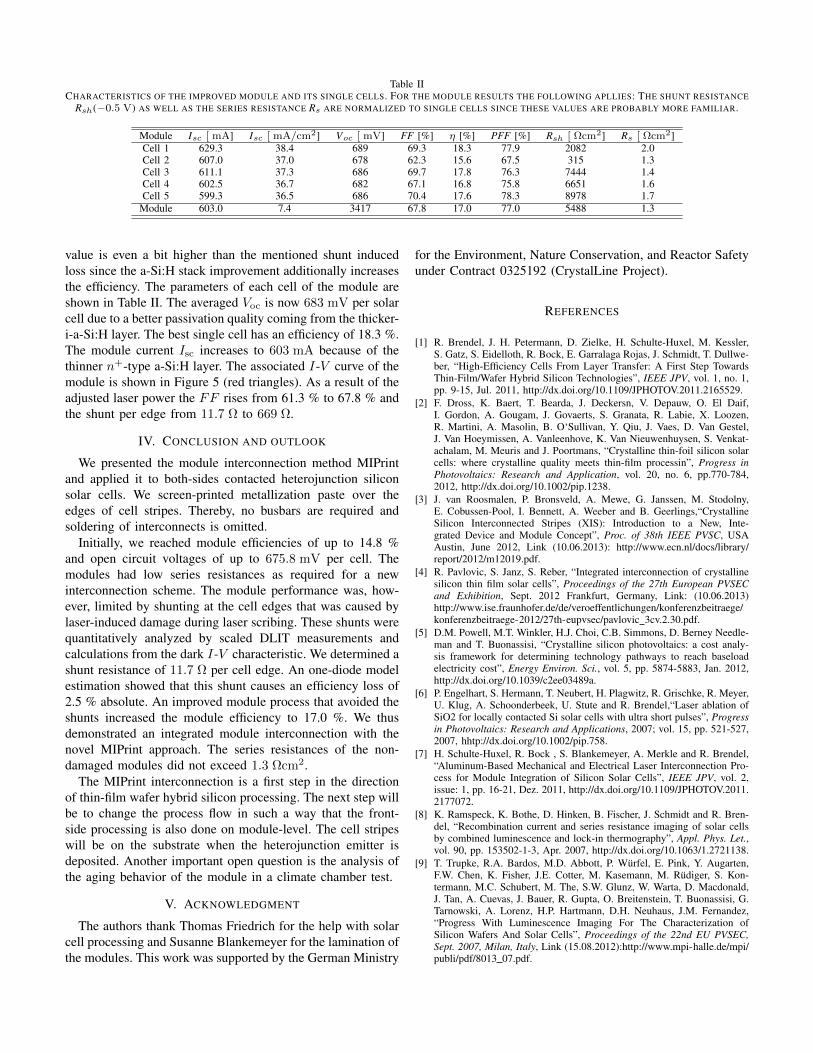
Table IICHARACTERISTICS OF THE IMPROVED MODULE AND ITS SINGLE CELLS. FOR THE MODULE RESULTS THE FOLLOWING APLLIES: THE SHUNT RESISTANCE
Rsh(−0.5 V) AS WELL AS THE SERIES RESISTANCE Rs ARE NORMALIZED TO SINGLE CELLS SINCE THESE VALUES ARE PROBABLY MORE FAMILIAR.
Module Isc [ mA] Isc [ mA/cm2] Voc [ mV] FF [%] η [%] PFF [%] Rsh [ Ωcm2] Rs [ Ωcm2]Cell 1 629.3 38.4 689 69.3 18.3 77.9 2082 2.0Cell 2 607.0 37.0 678 62.3 15.6 67.5 315 1.3Cell 3 611.1 37.3 686 69.7 17.8 76.3 7444 1.4Cell 4 602.5 36.7 682 67.1 16.8 75.8 6651 1.6Cell 5 599.3 36.5 686 70.4 17.6 78.3 8978 1.7
Module 603.0 7.4 3417 67.8 17.0 77.0 5488 1.3
value is even a bit higher than the mentioned shunt inducedloss since the a-Si:H stack improvement additionally increasesthe efficiency. The parameters of each cell of the module areshown in Table II. The averaged Voc is now 683 mV per solarcell due to a better passivation quality coming from the thicker-i-a-Si:H layer. The best single cell has an efficiency of 18.3 %.The module current Isc increases to 603 mA because of thethinner n+-type a-Si:H layer. The associated I-V curve of themodule is shown in Figure 5 (red triangles). As a result of theadjusted laser power the FF rises from 61.3 % to 67.8 % andthe shunt per edge from 11.7 Ω to 669 Ω.
IV. CONCLUSION AND OUTLOOK
We presented the module interconnection method MIPrintand applied it to both-sides contacted heterojunction siliconsolar cells. We screen-printed metallization paste over theedges of cell stripes. Thereby, no busbars are required andsoldering of interconnects is omitted.
Initially, we reached module efficiencies of up to 14.8 %and open circuit voltages of up to 675.8 mV per cell. Themodules had low series resistances as required for a newinterconnection scheme. The module performance was, how-ever, limited by shunting at the cell edges that was caused bylaser-induced damage during laser scribing. These shunts werequantitatively analyzed by scaled DLIT measurements andcalculations from the dark I-V characteristic. We determined ashunt resistance of 11.7 Ω per cell edge. An one-diode modelestimation showed that this shunt causes an efficiency loss of2.5 % absolute. An improved module process that avoided theshunts increased the module efficiency to 17.0 %. We thusdemonstrated an integrated module interconnection with thenovel MIPrint approach. The series resistances of the non-damaged modules did not exceed 1.3 Ωcm2.
The MIPrint interconnection is a first step in the directionof thin-film wafer hybrid silicon processing. The next step willbe to change the process flow in such a way that the front-side processing is also done on module-level. The cell stripeswill be on the substrate when the heterojunction emitter isdeposited. Another important open question is the analysis ofthe aging behavior of the module in a climate chamber test.
V. ACKNOWLEDGMENT
The authors thank Thomas Friedrich for the help with solarcell processing and Susanne Blankemeyer for the lamination ofthe modules. This work was supported by the German Ministry
for the Environment, Nature Conservation, and Reactor Safetyunder Contract 0325192 (CrystalLine Project).
REFERENCES
[1] R. Brendel, J. H. Petermann, D. Zielke, H. Schulte-Huxel, M. Kessler,S. Gatz, S. Eidelloth, R. Bock, E. Garralaga Rojas, J. Schmidt, T. Dullwe-ber, “High-Efficiency Cells From Layer Transfer: A First Step TowardsThin-Film/Wafer Hybrid Silicon Technologies”, IEEE JPV, vol. 1, no. 1,pp. 9-15, Jul. 2011, http://dx.doi.org/10.1109/JPHOTOV.2011.2165529.
[2] F. Dross, K. Baert, T. Bearda, J. Deckersn, V. Depauw, O. El Daif,I. Gordon, A. Gougam, J. Govaerts, S. Granata, R. Labie, X. Loozen,R. Martini, A. Masolin, B. O‘Sullivan, Y. Qiu, J. Vaes, D. Van Gestel,J. Van Hoeymissen, A. Vanleenhove, K. Van Nieuwenhuysen, S. Venkat-achalam, M. Meuris and J. Poortmans, “Crystalline thin-foil silicon solarcells: where crystalline quality meets thin-film processin”, Progress inPhotovoltaics: Research and Application, vol. 20, no. 6, pp.770-784,2012, http://dx.doi.org/10.1002/pip.1238.
[3] J. van Roosmalen, P. Bronsveld, A. Mewe, G. Janssen, M. Stodolny,E. Cobussen-Pool, I. Bennett, A. Weeber and B. Geerlings,“CrystallineSilicon Interconnected Stripes (XIS): Introduction to a New, Inte-grated Device and Module Concept”, Proc. of 38th IEEE PVSC, USAAustin, June 2012, Link (10.06.2013): http://www.ecn.nl/docs/library/report/2012/m12019.pdf.
[4] R. Pavlovic, S. Janz, S. Reber, “Integrated interconnection of crystallinesilicon thin film solar cells”, Proceedings of the 27th European PVSECand Exhibition, Sept. 2012 Frankfurt, Germany, Link: (10.06.2013)http://www.ise.fraunhofer.de/de/veroeffentlichungen/konferenzbeitraege/konferenzbeitraege-2012/27th-eupvsec/pavlovic 3cv.2.30.pdf.
[5] D.M. Powell, M.T. Winkler, H.J. Choi, C.B. Simmons, D. Berney Needle-man and T. Buonassisi, “Crystalline silicon photovoltaics: a cost analy-sis framework for determining technology pathways to reach baseloadelectricity cost”, Energy Environ. Sci., vol. 5, pp. 5874-5883, Jan. 2012,http://dx.doi.org/10.1039/c2ee03489a.
[6] P. Engelhart, S. Hermann, T. Neubert, H. Plagwitz, R. Grischke, R. Meyer,U. Klug, A. Schoonderbeek, U. Stute and R. Brendel,“Laser ablation ofSiO2 for locally contacted Si solar cells with ultra short pulses”, Progressin Photovoltaics: Research and Applications, 2007; vol. 15, pp. 521-527,2007, hhtp://dx.doi.org/10.1002/pip.758.
[7] H. Schulte-Huxel, R. Bock , S. Blankemeyer, A. Merkle and R. Brendel,“Aluminum-Based Mechanical and Electrical Laser Interconnection Pro-cess for Module Integration of Silicon Solar Cells”, IEEE JPV, vol. 2,issue: 1, pp. 16-21, Dez. 2011, http://dx.doi.org/10.1109/JPHOTOV.2011.2177072.
[8] K. Ramspeck, K. Bothe, D. Hinken, B. Fischer, J. Schmidt and R. Bren-del, “Recombination current and series resistance imaging of solar cellsby combined luminescence and lock-in thermography”, Appl. Phys. Let.,vol. 90, pp. 153502-1-3, Apr. 2007, http://dx.doi.org/10.1063/1.2721138.
[9] T. Trupke, R.A. Bardos, M.D. Abbott, P. Wurfel, E. Pink, Y. Augarten,F.W. Chen, K. Fisher, J.E. Cotter, M. Kasemann, M. Rudiger, S. Kon-termann, M.C. Schubert, M. The, S.W. Glunz, W. Warta, D. Macdonald,J. Tan, A. Cuevas, J. Bauer, R. Gupta, O. Breitenstein, T. Buonassisi, G.Tarnowski, A. Lorenz, H.P. Hartmann, D.H. Neuhaus, J.M. Fernandez,“Progress With Luminescence Imaging For The Characterization ofSilicon Wafers And Solar Cells”, Proceedings of the 22nd EU PVSEC,Sept. 2007, Milan, Italy, Link (15.08.2012):http://www.mpi-halle.de/mpi/publi/pdf/8013 07.pdf.

[10] R. Gogolin, R. Ferre, M. Turcu, N.-P. Harder, “Silicon heterojunctionsolar cells: Influence of H2-dilution on cell performance”, Solar EnergyMaterials and Solar Cells, vol. 106, pp. 47-50, Nov. 2012, http://dx.doi.org/10.1016/j.solmat.2012.06.001.
[11] More information under: http://www.pv-tools.de/, (Jun. 2013).[12] D. Hinken, S. Schinke, S. Herlufsen, A. Schmidt, K. Bothe and
R. Brendel, “Experimental setup for camera-based measurements ofelectrically and optically stimulated luminescence of silicon solar cellsand wafers”, Rev. Sci. Instrum., vol. 82, pp. 033706-1-9, 2011, http://dx.doi.org/10.1063/1.3541766.
[13] D. Pysch, A. Mette; S.W.Glunz, “A review and comparison of differentmethods to determine the series resistance of solar cells”, Solar EnergyMaterials & Solar Cells, vol 91, pp. 1698-1706, Jul. 2007, http://dx.doi.org/10.1016/j.solmat.2007.05.026.
[14] O. Breitenstein, W. Warta and M. Langenkamp, Lock-in Thermography,2nd edition, Springer, 2010, pp. 181.
[15] S. Steingrube, O. Breitenstein, K. Ramspeck, S. Glunz, A. Schenk and P.P. Altermatt, “Explanation of commenly observed shunt currents in c-Sisolar cells by means of recombination statistics beyond the Shockley-Read-Hall approximation”, Journal of Apllied Physics, vol. 110, pp.014515-1-10, 2011.