modules for controlled power distribution in an electric
TRANSCRIPT

Modules for Controlled Power Distribution in an Electric Vehicle
ECE 445 Final Report Spring 2019
Team 11: Siye Cen, Amalia Dungey, Richa Vijayvergiya
TA: Christopher Horn
2 May 2019

Abstract This paper details the process and results of a project to design a monitored and regulated low voltage (LV) bus board for the solar cars of the Illini Solar Car (ISC) team. Illini Solar Car designs and builds a new car every two years and the competitions they attend require the car’s electronics to be reliable and efficient over thousands of miles on the road. The LV bus board provides power to over ten printed circuit boards (PCBs) on the car, and the new design is able to monitor and switch up to ten connections on the LV bus independently. The board uses many automotive standard components, and multiple copies of the board can run on one solar car, which facilitates the distributed system of a road-legal car.
2

Table of Contents
1. Introduction 5 1.1 Purpose 5 1.2 Background 5 1.3 Functionality 5 1.4 Subsystem Overview 6
2. Design 7 2.1 Power Module 7
2.1.1 Power Protection 7 2.1.2 USB Power Input 8 2.1.3 Voltage Reference and Conversion 8
2.2 Microcontroller Unit 9 2.3 The 12V Outputs 10 2.4 Switching Module 10 2.5 Current Sense 11 2.5 Voltage Monitoring Module 12 2.6 Debug Status LED 13 2.7 CAN Transceiver 13 2.8 Firmware 13
3. Design Verification 15 3.1 Power Protection & Conversion 15
3.1.1 Power Protection 15 3.1.2 USB Power Input 15 3.1.3 Voltage Reference and Conversion 15
3.2 Microcontroller Unit 15 3.3 The 12V Outputs 15 3.4 Switching Module 16 3.5 Current Sense 16
3.5.1 Calibration and Verification 16 3.5.1 Source of Uncertainties 17
3.6 Voltage Monitor 17 3.7 Debug Status LED 18 3.8 CAN Transceiver 18 3.9 Firmware 18
4. Cost and Schedule 19 4.1 Labor 19 4.2 Parts 19
3

4.3 Schedule 19
5. Conclusion 21 5.1 Accomplishments 21 5.2 Uncertainties 21 5.3 Future Work/Alternatives 21
5.3.1 PCB Layout 21 5.3.2 Switching Module 21
5.4 Ethical Considerations 21
6. References 23
7. Appendix A - Full Schematic and PCB 24
8. Appendix B - Requirements and Verification Tables 26 9. Debug/Status LEDs 30
9. Appendix C - Parts 31
4

1. Introduction
1.1 Purpose The objective of this project is to improve efficiency by increasing the down-time of printed circuit boards (PCBs) powered by a low voltage bus; thus decreasing power consumption of the Illini Solar Car (ISC) team’s solar electric vehicles. It will allow the power distribution system (PDS) to individually monitor and control connections to the 12V bus of the solar cars. The existing 12V bus, from which most of the vehicle’s PCBs are powered, is just 12 connectors in parallel, with no protection circuitry, power monitoring, or switching. The implementation of our project will allow for specific control of the boards that are powered, which we estimated can improve our efficiency by 1.81%. After updating and redesigning our LV bus board, we were able to control the connections to the bus independently, each with current and voltage sensing, however we are still working on testing and calculating the efficiency this will provide.
1.2 Background The low voltage (LV) system of ISC’s solar electric vehicles includes the dashboard, steering wheel, power distribution system control, lights, and telematics and data logging. All of these systems are necessary for a road-legal vehicle but not all are required by the competitions in which the team competes. Additionally, certain systems are not required at all during the competitions’ allotted charging and checkpoint times, during which the solar car may not be driven and the team has an opportunity to simply store energy for the next round of driving. For these reasons, we first need a protected and regulated LV bus in order to ensure low power consumption. We also need a LV bus board that is capable of switching its connections on and off depending on the needs of the car. For instance, if we can switch the driver displays off when there is no driver in the car, we will save approximately 360 mW of energy (30mA approximate current draw measured by multimeter at 12V). This can add up over the race.
1.3 Functionality Project functionality must include switching power to ten connections, sensing current on each of the switched connections, and sensing the voltage on the LV bus. The ability to sense this data is crucial to finding out which systems will save the most power when we turn them off. It must also have communication with the Controller Area Network (CAN) on the car, so other systems such as telemetry can collect data about the performance of the LV bus. All of the switched and monitored connections must default on in order to ensure that all electrical subsystems have power at startup.
5

1.4 Subsystem Overview There are three major parts to the LV system that we developed as can be seen in our block diagram in Figure 1. The first is the power protection and conversion circuitry. It is meant to ensure that the 12V that is delivered via the PCB is reliable, and can be converted to power lower voltage components such as the microcontroller unit (MCU), which is the second major subsystem. The MCU takes care of voltage and current monitoring and communicating with the rest of the car over CAN. The third subsystem is our switched connections. Each connection should be able to send requested data like the voltage and current to the MCU, as well as turn on and off on command.
Figure 1: Block Diagram
6

2. Design The project contains extensive upgrades to the current 12V bus for Illini Solar Car electrical system. The new low voltage (LV) bus has a microcontroller unit (MCU) that is used to control power to all the other subsystems that run on the LV bus of the car. Subsystems include, but are not limited to, steering wheel, lights, power distribution, displays, and telemetry. Our main objective is to improve efficiency of our car. It is accomplished by being able to turn each output connection “on” or “off” on the 12V bus independently. This is done by implementing a high side driver to each of the switched connections on the low voltage bus and having the MCU communicate with each one separately (Infineon). The MCU receives signals from the rest of the car and the person driving it via Controller Area Network (CAN), and it controls each high side driver accordingly. Aside from switching ability, we also have current and voltage monitors on the low voltage bus. There is a current sense on each of the power switches in order to track which LV part of the car is consuming the most power. By monitoring and gathering this data the team can then move to design those specific areas of the car more efficiently. We have voltage sensing on the 12V bus after the power protection circuit in order to monitor what voltage the bus is normally operating at so we can accurately calculate power consumption. The main purpose of our 12V board is to control which parts of the car receive power in order to ration energy during tests and competitions, and to reveal what low voltage systems consume significant power. The block diagram on Figure 1 gives an overview of the system and shows how each component of the low voltage bus board communicate with each other using signal and how power flows in the system. Each block will be analyzed in more detail in the following sections of this report. Appendix A includes the top view of the schematic and the front and back view of the low voltage bus board PCB. They give the electrical and physical layout of the system.
2.1 Power Module There are four parts within the power module: power protection circuit, USB power input, voltage reference, and voltage conversion. The low voltage bus 12V input is from the DC/DC converter inside the battery box, which is outside the scope of our project. We are mindful of the fact that the existing DC/DC converter current limit is 8.5 A, which means all of the input circuitry and protection should be able to handle that current, but the design may change. We have designed our board being careful to limit the current to the boards to which it supplies power and not being concerned with the main DC/DC converter, which has its own overcurrent protection.
2.1.1 Power Protection The range of possible voltages we could get on 12V bus based on DC/DC converter output range from 9 to 18V (vicorpower, 2019). The power protection circuit we have on the low voltage bus board has several functions. It protects against overvoltage beyond 18V, overcurrent beyond 10A, and reverse voltage from 0 to -8V. The input connector on the board is a 4-pin KK396 with two pins on the side connected to ground and two middle pins connect to DC/DC converter with 12V output. This structure guarantees that no matter which way the connector is plugged in, there will not be a reverse negative voltage input.
7
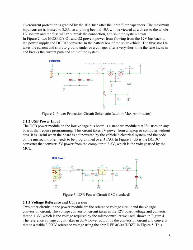
Overcurrent protection is granted by the 10A fuse after the input filter capacitors. The maximum input current is limited to 8.3A, so anything beyond 10A will be viewed as a threat to the whole LV system and the fuse will trip, break the connection, and shut the system down. In Figure 2, two MOSFETs Q1 and Q2 prevent power from flowing from the 12V bus back to the power supply and DC/DC converter in the battery box of the solar vehicle. The thyristor D4 takes the current and short to ground under overvoltage, after a very short time the fuse kicks in and breaks the current path and shut of the system.
Figure 2: Power Protection Circuit Schematic (author: Max Armbruster)
2.1.2 USB Power Input The USB power module on the low voltage bus board is a standard module that ISC uses on any boards that require programming. This circuit takes 5V power from a laptop or computer without data. It is useful when the board is not powered by the vehicle’s electrical system and the code on the microcontroller needs to be programmed over JTAG. In Figure 3, U5 is the DC/DC converter that converts 5V power from the computer to 3.3V, which is the voltage used by the MCU.
Figure 3: USB Power Circuit (ISC standard)
2.1.3 Voltage Reference and Conversion Two other circuits in the power module are the reference voltage circuit and the voltage conversion circuit. The voltage conversion circuit takes in the 12V board voltage and converts that to 3.3V, which is the voltage required by the microcontroller we used, shown in Figure 4. The reference voltage circuit takes in 3.3V power output by the conversion circuit and converts that to a stable 3.000V reference voltage using the chip REF3030AIDBZR in Figure 5. This
8

series reference voltage IC output has 0.2% accuracy, which is required by the microcontroller (Series Voltage Reference IC datasheet).
Figure 4: DC/DC 12V to 3.3V Conversion Circuit (ISC standard)
Figure 5: 3.000V Reference Voltage Circuit (ISC standard)
2.2 Microcontroller Unit The microcontroller reads messages from the CAN bus transceiver and controls outputs, such as LED indicators and switch controls, based on those messages. The microcontroller we used for our design is a LPC1517, which is a 32-bit ARM Cortex-M microcontroller from the LPC15xx family and it complies with the ISC code base (wiki.illinisolarcar, 2019). It is a 64 pin microcontroller with enough general purpose input/output (GPIO) pins and analog-digital converters (ADC). It also supports CAN communication, which is what we need in order for the board to talk with the rest of the vehicle. For the low voltage bus board, we used 14 GPIO pins for ten high side drivers and four debugging LEDs. In addition, we used 11 ADC pins for ten current senses and one voltage sense. The MCU is attached to a reset button to restart the firmware and communication with CAN. More details are shown on the schematic in the figure below. The schematic we used for MCU unit is based on an ISC standard circuit for LPC15xx family. In order to use it for our project, the schematic was modified for the 64 pin MCU on the low voltage bus board. The advantages of the LPC15xx family include low power consumption and capability of running mbed, an operating system for internet-connected devices based on 32-bit ARM Cortex-M microcontrollers. The mbed application programming interface (API) is very useful when handling the ADC and GPIO pins on the microcontroller.
9

Figure 6: Microcontroller Unit Schematic
2.3 The 12V Outputs The low voltage bus board is designed to have a sufficient number of connections on the 12V bus for all boards on the car, as well as extra ones for jump start and other debugging purposes. As shown in Figure 10, it has four unswitched and unmonitored connectors directly on the 12V bus. They are used for critical subsystems that need to stay on any time the car is on, such as the telematics system. Two of them are KK396 and two of them are KK254. In addition, there are ten switched and current monitored connector outputs on the low voltage bus, five of which are KK254 and five of which are KK396. These ten connectors are individually controlled by the MCU. They are also labeled with numbers for clear identification. Molex’s KK254 and KK396 families are two types of connectors with slightly different current capabilities. They are useful since some of the subsystems on the car such as the boards controlling lights draw higher current than boards like the dashboard control. Similar to the 4-pin input connector, which has two +12V pins in the middle and two ground pins on the outside, all the connectors for the outputs have a 3-pin structure with two sides connected to ground and the middle connected to +12V. This prevents accidental reverse polarity from a backwards connection, so it will protect the boards that it is powered.
2.4 Switching Module There are various choices when designing the switch module such as P channel MOSFET, N-Channel MOSFET, etc. However, there are many drawbacks to using simple MOSFETs on a board that needs to go on an electric vehicle for a race. A PMOS usually has higher turn-on resistance and relatively low efficiency. An NMOS requires supporting circuitry and an external voltage source to turn on. Often times the supporting circuitries are bulky and expensive. Therefore, instead of a simple MOSFET, we chose a high side driver for the low voltage bus board. BTS5010-1EKB is an automotive-grade high side power switch, also known as high side
10

driver. It is a single channel power switch with an N channel power MOSFET with a charge pump and supporting circuitry. This makes controlling the output very simple for us, as we can connect one pin to 3.3V. In addition to simplicity and compact size, this chip has high efficiency due to a low Rds on (approximately 10mΩ). It has a nominal load current of 10A and an operating voltage range of 5-28V. It is an ideal fit for our board, which has an operating voltage from 9-18V. To turn the power switch on, we simply set the IN (input) and DEN (diagnostic enable) pin high (in this case 3.3V from MCU GPIO pins). Setting the diagnostic enable pin high enables the current sensing output, which we discuss in the next section.
Figure 7: Switching Module Schematic
2.5 Current Sense The high-side power switch BTS5010-1EKB has a built-in current sense. Pin 6 on the BTS5010 outputs a small sense current that is proportional to the actual load current on its output. Pin 6’s output connects to an external sense resistor of 1.2kΩ and a filtering capacitor of 100pF. These values are recommended in the application notes for the chip. The sense resistor helps to convert the current to a voltage value that is well within the range of the ADC’s capability of the microcontroller. The MCU API will read a floating point number between 0 and 1 that represents the input voltage as a percentage of the reference voltage; our reference voltage on the board is 3.000V +/- 0.2%. Calculations are shown in the following equations. is a coefficient thatK ILIS relates sense and load current. For a BTS3010-1EKB chip, this value is typically 3000. Discrepancies exist between the typical value and empirical value, based on the load current. As shown in the Figure 9, the K value has a trumpet shape with respect to the load current. As current increases, the sensor is more accurate. For a low current value below 0.5A, the coefficient deviates from the nominal value. The current sense on the high side driver works, and we will discuss the calibration and verification of it in Section 3. The sensed current reading is in mA for easier manipulation of the data in firmware code.
(1) (A)Isensed = Rsense
ADC ×Vf loat ref = 1.2kADC × 3.00Vf loat
11

(2) (mA) I load = 1000 × K ILIS × Isensed
Figure 8: Built-in Current Sense on High Side Driver
Figure 9: K value trumpet for the Built-in current sense
2.5 Voltage Monitoring Module To monitor the voltage on the 12V bus, we used a voltage divider with a 33kΩ resistor and a 6.8kΩ resistor. In order to reach the desired tolerance of 12V +/- 0.01V, we chose resistor ERA-6ARW333V and ERA-6ARW682V with low tolerance of +/-0.05%. This method of voltage monitoring has low losses since the resistance is very high and very little current runs through the resistors. The equations below show how to calculate the voltage on the 12V bus. Similar to current sense, the is a value from 0 to 1 that represents the input voltage as a percentage of theADC f loat reference voltage 3.000V. This voltage can be used to calculate the actual bus voltage. The output of the voltage sense is an integer in mV. The change of units here is useful for easier manipulation of the number in the code.
(3)×1000 (mV )V LV Bus = ADC f loat × V ref × R18
R + R15 18
12

(4) × 3.000V × ×1000 (mV )V LV Bus = ADC f loat 6.8k
33k + 6.8k
Figure 10: Voltage Monitor and Debugging LEDs
2.6 Debug Status LED There are four debugging LEDs on the board. They are connected to four GPIO pins on microcontroller. They are useful during the development stage. By changing the LED pattern whenever we flash the code onto the board, it helps ensure that we are running the version of the code we want. In addition, one of the LEDs blinks whenever the CAN heartbeat is sent, making sure that we are communicating with the CAN and the rest of the car successfully and that the code is not stuck in any loop.
2.7 CAN Transceiver The low voltage bus board communicates with the rest of the vehicle system via Controller Area Network (CAN). Therefore, a CAN transceiver with galvanic isolation is implemented on the board. The CAN transceiver module is a standard circuit for ISC. CAN is an automotive standard communication and it is used on all electrical systems on the solar car. There are also existing mbed APIs supporting the CAN communication.
Figure 11: CAN Transceiver Schematic
2.8 Firmware We wrote the firmware for the MCU in C++. The firmware has simple timers to trigger sensing the currents and voltage and then sending the data to the CAN bus. It also has a function run every time it runs the main loop to check for any new CAN message received with the ID for the
13

switch change request. If one of these requests is sent, it will change the status of the digital I/O pins connected to the enable pins on the high side drivers, and it will report the new status of the connections. The sensing firmware has some calibration from the initial values we read from the ADCs, since they were consistently offset from the actual values read by a multimeter. Equations 1-4 from previous sections showing the calculations we used. We used these calculations to convert the ADC readings accessed through the mbed API to unsigned integers that are related to the actual voltage and currents on the board by powers of 10. The unsigned integer format is easy to work with and 16-bit unsigned integers are plenty of space to encode the information about up to 18V in mV and up to 5A in mA.
14

3. Design Verification
3.1 Power Protection & Conversion
3.1.1 Power Protection The overvoltage and reverse voltage tests were performed on power protection circuitry. The board successfully turns on starting at 9V. In order to test for overvoltage, we have to start from above the maximum voltage that it will normally see. Starting from 12V, increase the voltage 1V at a time and observe the current reading with all output connectors at open load. After we reach a voltage limit of 17V, increase by 0.1V. At 18.7V (the voltage limit), the current rises to 0.1A (current limit) and the voltage from the power supply drops to 0.088V. This indicates we have a short from the input to the ground through thyristor D4 (Figure 2) in the schematic. On an operating car, without the power supply’s current limit, this will trip the fuse and shut down the system. In short, overvoltage test is successful, and it is activated at any input voltage above 18.7V. For the reverse voltage test, connect the input to a power supply with a current limit of 100mA. The ground of the board is connected to the positive end and the input power in is connected to the ground of the power supply. Start from the voltage limit of 0V and increase by 1V increments, observe, and record current data. For positive voltages below 8V, the current input measured is 0.00A, which is expected behavior of the power protection circuit under reverse polarity. When the voltage limit is increased to 9V, we observe a current draw of 0.100A and a voltage input of 0.7V. This indicates that the reverse polarity protection works for any reverse voltage magnitude under 9V. A reverse voltage greater than 9V will cause the fuse to trip and the low voltage bus will be disconnected from the DC/DC converter inside the vehicle battery box.
3.1.2 USB Power Input Plug a USB-A to micro USB-B cable into the computer and the board. The board debug lights should turn on. If you measure voltage across ground and any pad at 3.3V, it should read around 3.3V.
3.1.3 Voltage Reference and Conversion Measure the voltage reference chip output when powering the board with 12V input. It should be 3.000V. Measuring it when the board is powered through the USB connection, only 5V, will result in only 2.88V, but if the board is powered through USB there are no 12V connections that are useful to measure, so the inaccuracy at that point is immaterial.
3.2 Microcontroller Unit After assembling the hardware, plug in the JTAG connection and USB and attempt to program the board with a blinking LED program. If successful, move on to testing each switch output and ADC input separately to verify the hardware functions.
3.3 The 12V Outputs Apply 12V at the input of the PCB power and measure the voltage at the unswitched outputs. Verify that the voltage at the unswitched outputs is within 0.5V of the input, to account for any protection diode voltage drops.
15

3.4 Switching Module Before performing the system test of controlling all the switches by the MCU, modular testing was done on each power switch chip separately. Here are the steps:
1) Assemble a set of BTS5010-1EKB chip, adding one input filter, one output filter, one output resistor, one current sense filter, and one current sense resistor at a time.
2) Power the 12V plane on the board, keep all output connectors with an open load. Probe the power pin on the corresponding output connector.
3) Attach the Switch control (SW_CTRL) pin to a 3.3V power supply by attaching it to a bulge wire. Keep power supply off until manually toggling the control input signal makes it on.
a. See whether the output (SW_Out) successfully follows the control signal. 4) Repeat the test for all 10 switches on the board and run the test for two boards. 5) If all of the previous test cases performed correctly, connect output connectors to high
power LEDs and current limit the power supply 0.100A. a. See whether the chip functions with a load.
Soldering issue came up when testing the first chip because of improper soldering of the pad on the bottom of the chip. It was resolved by carefully applying hot air and enough solder on the pad. Once we verify the chips worked individually, we test them together by hard-coding the MCU. Set each of the switches to alternate between on and off states, and repeat this test for both version for the board we built. These were our test results the first time:
1. Connectors 1, 2, 3, 5, 6, 9, 10 work 2. Connector 4: no matter what the code does, the pin is constantly at 2.24V instead of 3.3V
or 0V. unable to turn the switch off. 3. Connectors 7 and 8: no matter what the code tells it to do, it is constantly at 0V. unable to
turn the switch on. To resolve the problem:
1. Connector 4: wrong pin label when creating the schematic, change #define in the code solved the problem. Wrong pin label at PIO1_10 on MCU, changed to be PIO1_9.
2. Connector 7 and 8: I2C pins on the MCU (PIO0_22/23) were unable to pull the output high→ added external pull up resistors on both pin (10kΩ) to solve the problem.
3.5 Current Sense Current sensing is a requirement on each of our connectors in order to monitor which subsystems of the LV bus are consuming the most power. In order to improve efficiency for the LV bus system, we need to know what systems we need to turn off during a low-power state for the car. We used the built-in current sense from the high side drivers we used and compared it to the actual values we measured using a multimeter.
3.5.1 Calibration and Verification The purpose of calibration and verification was to compare the current sensor with the actual values that we saw from a multimeter. If the sensor was working properly, both the current read through code and the current read through the multimeter should have given the same values.
16
However, this was not the case and we had to adjust for this difference in our code. Figure 12 compares the values we read before and after calibration. Use equation from section 2.5 and code in firmware using ADC API. To test current sense:
1. Limit power supply to 12V and 0.100A, and power the board 2. Set the connector to be constantly on in the code 3. Plug the output connector to a high-power LED 4. Increase the current limit and watch the LED become brighter and record the current
reading from the code and the actual current input by the power supply. 5. Subtract quiescent current (0.071A( from the power supply current and compare the
resulting current with the code current output. 6. Plot actual-load current against sensed-load current 7. Adjust the scale factor in the code
a. Initial equation: 1000 * (30/4) * (ADCfloat) (5) b. After calibration: 1000 * (30/4) * (ADCfloat) + 120 (6)
8. Use the new code, repeat step 1-7.
Figure 12: Current Sense before and after Calibration
3.5.1 Source of Uncertainties There are many sources of inaccuracy of the theoretical current sense calculation. Two of
the major ones are the manufacturing defects of the sense resistors and K value of the high side drivers.
1. Sense resistor has 0.1% tolerance, too high for the accuracy we want to achieve 2. K value of the high side driver has a trumpet shape and changes more under low current.
To improve: pick resistors with lower tolerance level; test more and find the K value under several load current and make the code to handle different current level.
3.6 Voltage Monitor Similar to the current sense, we also did calibration for the voltage sense.
Initial equation: ADCfloat* 3.00 * [(33k+6.8k) ÷ 6.8k] * (1000+0.5) (7) After calibration: ADCfloat * 3.00 * [(33k+6.8k) ÷ 6.8k] * (1000+120) (8)
17

(9)rror due to tolerance ×100% .08% .05%e = 0.01V12.00V = 0 > 0
3.7 Debug Status LED Debug LEDs are multi-purpose LEDs that we use to help debug our code. All of them were able to blink at rates up to four times a second, which is sufficient for the time intervals that we set the functions for the sense readings and CAN heartbeat to run.
3.8 CAN Transceiver The CAN transceiver was simple to verify on the test bench. We plugged in the board to the CAN bus on the bench, which had the dashboard and PDS control also connected, and plugged in the CAN bus analyzer. Figure 13 is a screenshot of the CAN bus analyzer interface software. The top window displays the last message from each CAN ID, and our board’s CAN IDs fo 0x502-0x506, 0x50F, 0x500, and 0x49 can be seen received by the CAN bus analyzer at the 2Hz and 1Hz (for 0x49) rates we set them to be in firmware. The message 0x500 is the last message that it received to command the high side drivers’ statuses, and we can see that it sent the message 0x501 in acknowledgement after it received message 0x500.
Figure 13: CAN Transceiver Interface
3.9 Firmware The firmware verification took place at the same time as the CAN transceiver verification. Because the code runs on the MCU without getting stuck in any loops and sent and received the correct CAN messages, as well as the correct data from the current and voltage sense (after calibration), it is a success.
18

4. Cost and Schedule
4.1 Labor The hourly rate was determined using the average salary for an electrical engineer that graduated from UIUC from the ECE Illinois website (Engineering Services, 2019). The average salary for a someone with a BS in Electrical Engineering from UIUC between 2014-2015 was $67,000.
(5)32.21/hour$6700052 weeks * 1 week
40 hours = $
Name Hourly Rate Total Hours Total Total * 2.5
Siye Lynn Cen $32.21 150 $4831.5 $12078.75
Amalia Dungey $32.21 150 $4831.5 $12078.75
Richa Vijayvergiya $32.21 150 $4831.5 $12078.75
Total $36236.25
Table 1: Labor Cost
4.2 Parts The total cost of all the parts we ordered, which include the PCBs and the components was $83.48. For a full break down, look at Appendix C. The main parts cost for the project is the PCB itself, which was sponsored for us by one of Illini Solar Car’s sponsors, Bay Area Circuits. For production runs, the cost of components would decrease by at least 33%, since buying parts in reels is much less expensive. For some discrete parts, the cost can decrease by 90% per part.
4.3 Schedule We started this schedule from Week 6 because that is when we started working on our own project instead of the presentations for projects that happened at the beginning of the semester.
Week # Lynn Amalia Richa
Week 6 (2/18) Design Document Design Document Design Document
Week 7 (2/25) Single & combined switch module schematic
Firmware process diagram finalized
Current sensing schematic for high-side driver
Week 8 (3/4) Schematic for switch & current monitor unit
Code outline, including CAN message structure
Power protection schematic for +12V bus
19

Week 9 (3/11) Combined bus board schematic
Finalize firmware code Voltage sensor schematic, send out all designs for review
Week 10 (3/18) Bus board layout with CAN & USB & MCU & LED
Review schematic, test CAN communication
Verify bill of materials
Week 11 (3/25) Layout review & Order boards
Order parts Order current and voltage sensing devices
Week 12 (4/1) Assemble 3 PCBs Test board communication: switch
Test the power protection and both sensors
Week 13 (4/8) Testing and validating switch default
Test board communication: sensors
Test high-side drivers with the current and voltage sensors, put it all together
Week 14 (4/15) Testing and validating switch independence
Test code stability Test current sense
Week 15 (4/22) LEDs to attach to all the connectors
CAN communication Test discrete current sense Final Paper
Week 16 (4/29) Final Presentation Final Paper
Final Presentation Final Paper
Final Presentation Final Paper
20

5. Conclusion
5.1 Accomplishments We were successful in meeting all of the requirements we set for this project except for stability. The current and voltage sense capabilities were both extremely precise, which means we can verify our data more easily. Lack of stability testing at this point means that we will not be able to put the system onto the solar car, but it can still run on the test bench.
5.2 Uncertainties The built-in current sense had the greatest uncertainties in the project. We were not able to compare it to a discrete current sense module as we had originally planned.There are many sources of inaccuracy of the theoretical current sense calculation. Two of the major ones are the manufacturing defects of the sense resistors and K values of the high side drivers.
1. Sense resistor has 0.1% tolerance which is too high for the accuracy we want to achieve 2. K value of the high side driver has a trumpet shape and changes more under low current.
To improve on our calculations, we could pick resistors with lower tolerance level, test more and find the K values under several load currents and adjust the code to handle different current levels.
5.3 Future Work/Alternatives
5.3.1 PCB Layout The layout of this board is a relatively simple design, which means that we placed all of the components on the front side of the board and routed them with debugging in mind and not compact size. This means that the board is much larger than can fit on the solar car, and would be more expensive to manufacture, since the PCB cost is a significant portion of the bill for parts
5.3.2 Switching Module The switch modules we chose performed with all loads we tested. The firmware we wrote set all of the connections to high by default but the hardware does not, so adding pull-up resistors would increase reliability in case of a code failure.
5.4 Ethical Considerations The IEEE Code of Ethics 7.8.1 (IEEE.org, 2019) that lays out the rules regarding health, safety, and public welfare will be the code of ethics we intend to follow. Building a solar electric vehicle from scratch is a very challenging task that comes with a lot of safety risks. From designing the proper PCBs with correct connections to machining all of the parts that will come together to make the car, a lot of problems have, and will, occur. Should there be injuries, we intend to take them seriously.
21

In our project we used some circuits that are part of ISC’s standard. These include the USB Power, Power Protection, and Conversion circuit. To give credit where credit is due, we always have a section for names on the full schematic, in accordance with IEEE standard 7.8.7. That way not only can people claim their work but should anyone have questions about a specific circuit, we know who to go to. We only worked with low voltages (+12V, logic levels) and nothing that would require more than 50V. By working with low voltage modules, we had an inherent level of safety. Within our project, we have current sensing on each of the connectors on our +12V bus in order to monitor the power that will be delivered. We also have power protection for each power input to mitigate the chance of damage to sensitive components, like the microcontroller. This was to be proactive and prevent problems before they materialize. Despite the relative safety in +12V power, we implemented a switching system that normally closed and failed closed instead of open.
22

6. References [1] Ieee.org. (2019). IEEE Code of Ethics. [online] Available at: https://www.ieee.org/about/corporate/governance/p7-8.html [Accessed 21 February 2019]. [2] Nxp.com, 2019. [Online]. Available: https://www.nxp.com/docs/en/data-sheet/LPC15XX.pdf. [Accessed: 09 March 2019]. [3] Recom-power.com, 2019. [Online]. Available: https://recom-power.com/pdf/Innoline/R-78E-0.5.pdf. [Accessed: 18 March 2019]. [4] Infineon.com, 2019. [Online]. Available: https://www.infineon.com/dgdl/Infineon-BTS5010-1EKB-DS-v02_00-EN.pdf?fileId=5546d4625a888733015aa42c62c7113e&fbclid=IwAR0kNreRk6W5R7K3Ju-enAaX7UXt-CN05_ZmIxJuOpWGkbUt-YnSxI9ajLs. [Accessed: 14 March 2019]. [5] Texas Instruments. 2019. [Online]. Available: http://www.ti.com/general/docs/suppproductinfo.tsp?distId=10&gotoUrl=http%3A%2F%2Fwww.ti.com%2Flit%2Fgpn%2Fref3012. [Accessed: 3 March 2019]. [6] Cdn.vicorpower.com. (2019). DC-DC Converter Module. [online] Available at: http://cdn.vicorpower.com/documents/datasheets/ds_110vin-micro-family.pdf [Accessed 21 Feb. 2019]. [7] Engineering Services, E. (2019). Salary Averages :: ECE ILLINOIS. [online] Ece.illinois.edu. Available at: https://ece.illinois.edu/admissions/why-ece/salary-averages.asp [Accessed 21 Feb. 2019]. [8] wiki.illinisolarcar. (2019). MCUXpresso Appendix & Notes. [online] Available at: https://wiki.illinisolarcar.com/wiki/tiki-index.php?page=MCUXpresso&highlight=reset [Accessed 21 Feb. 2019].
23

7. Appendix A - Full Schematic and PCB
Figure 14: Top Level Schematic for LVBusBoard_v2
Figure 15: PCB Layout – Front
24
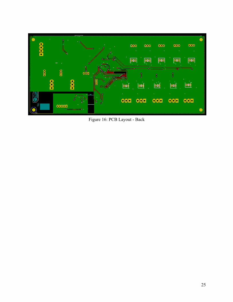
Figure 16: PCB Layout - Back
25

8. Appendix B - Requirements and Verification Tables 1. Input Protection and Conversion
Requirement Verification Completeness
Voltage after protection should not exceed 14V(+/-0.1V) for inputs from 9-18V.
1. Sweep voltage at the input connector from 9-18V using an oscilloscope
2. Voltmeter at the output of the protection circuitry should not read more than 14V(+/-0.1V).
Yes
This module should convert 12V for the LV bus to 3.3V(+/-0.02V) for IC power.
1. Voltmeter at the output of the conversion circuitry should read value 3.3V(+/-0.02V).
Yes
2. Voltage Monitoring Module
Requirement Verification Completeness
This module should have LV bus voltage sensing ability and can report to MCU when queried.
1. Request bus voltage data using the MCU.
Yes
The reported voltage sensing data should have +/-0.01V precision.
1. Connect external oscilloscope at testing point on PCB.
2. Compare voltage reading of the monitoring module with external oscilloscope reading.
Yes
3. Microcontroller Unit
Requirement Verification Completeness
26

MCU is able to send and receive messages
1. Ensure no other processes are happening
2. Send a message to a specific module 3. Verify that the receiver then acts as it
was instructed
Yes
MCU has >10 GPIO pins
1. Confirm existence on datasheet Yes
MCU can be programmed over JTAG SWD
1. Verify with the datasheet 2. Upload a hello world or blinking
lights program to the MCU through the JTAG connection
3. Verify the Debug LEDs flash in the programmed sequence as the code runs
Yes
When pressed, the Reset button should restart the firmware on the MCU.
1. Press the button 2. The on-board debug LEDs will
indicate beginning of the code.
Yes
4. Switching Module
Requirement Verification Completeness
While the 12V input is powered, the default state of the switch connections is that they are connected/on.
1. Connect the 12V input while the communication circuitry is disconnected.
2. Verify that each module connection has 12V power.
3. Connect the communication circuitry but do not send any commands to the switching chip.
4. Verify that each module connection has 12V power.
5. Command the chip to switch off the power to all modules.
6. Disconnect the communication circuitry and verify that each connection has 12V power after 5 seconds.
Yes
27

FET in each module should be able to turn on and off individually within 0.25 seconds in response to signals and driver input processed by MCU
1. Connection should be enabled if the CAN message signals MOSFETs to do so within 0.25 second. Output voltage should be tested under following conditions (various test cases):
i. Command the chip to stop power to all 10 connections.
ii. Toggle firmware through 10 states: one connection powered at a time.
iii. Cycle firmware through five other possible combination of 10 connections off and on. Check that the outputs are at 12V when they are supposed to be on.
Yes
5. Current Sense
Requirement Verification Completeness
Each of ten current monitoring modules connected should be able to report current information to the MCU when queried.
1. Request each module’s data using the MCU.
Yes
At normal voltage (+12V) current monitoring on each output connection should be within +/-10mA accuracy ranging from 0.4A to 5A.
1. Test module with different loads within range: low point and upper bound
2. Verify loads can draw constant 500 mA and 5 A at 12V.
3. Connect loads and external oscilloscope at each output.
4. Compare current reading of the monitoring module with external meter reading.
No
6. 12V Outputs
28

Requirement Verification Completeness
Use two types of standardized connectors compatible with current car: 10 switched output connectors (5+5) on the board to handle different currents and wire types on subsystem PCBs.
1. Check the PCB design and schematic to verify correct number of connections
2. Plug into the existing electrical system test bench to verify compatibility.
Yes
One KK396 input connector (easily identifiable) and 4 unswitched connectors.
1. Check the PCB design schematic and layout.
Yes
7. Firmware
Requirement Verification Completeness
Latch the switching state until a new signal is received or the board loses power.
1. Send command to switch every other module on, every other module off.
2. Wait for 2 hours 3. Meter the module connections to
verify they are the same as when the command was initially set
No
Switch the power on each of 10 connectors independently
1. Connection should be enabled if the CAN message signals MOSFETs to do so. Output voltage should be tested when toggle firmware through 10 states: one connection powered at a time.
Yes
8. CAN Transceiver
Requirement Verification Completeness
29

Should be able to withstand +/- 18V spikes on the CAN_HIGH and CAN_LOW pins.
1. Use oscilloscope to send +/- 18V on the CAN bus pins
2. Measure the voltage at the receiving end to monitor what is received at the pins
3. Use a CAN bus analyzer to verify the chip can still send and receive messages
Yes
9. Debug/Status LEDs
Requirement Verification Completeness
On-board LEDs should be able to turn on and off based on firmware for debugging and status indication.
1. Test MCU can turn on and off LEDs with GPIO.
2. Test LED can indicate fault state.
Yes
10. USB Power Input
Requirement Verification Completeness
The 3.3V connections on the PCB should have power.
1. Connect the board to a computer via USB.
2. Check that the 3.3V indicator LED is on.
Yes
30

9. Appendix C - Parts
31