mohammed m. albannay - qut · mohammed m. albannay b.eng (hons.), queensland university of...
TRANSCRIPT

Array of antenna arrays
by
Mohammed M. Albannay
B.Eng (Hons.), Queensland University of Technology
A thesis submitted in fulfillment for the degree of
Masters of Engineering (Research)
Science and Engineering Faculty
Queensland University of Technology
2014


Copyright © 2014 Mohammed M. Albannay
All rights reserved
Queensland University of Technology


Keywords
Antenna arrays
Array feed network
Beam forming
Mutual coupling
Decoupling and matching networks
Passive microwave circuits
Printed circuit board fabrication
v


Abstract
Antenna array capabilities can be enhanced by increasing the number of elements employed.
This inevitably results in a physically larger array, as reducing interelement separation results
in mutual coupling between neighbouring radiation radiators which consequently degrades the
array’s performance. This thesis explores the concept of an array of subarrays, where conven-
tional array elements (part of a uniform circular array) are replaced with a compact uniform
circular array; thereby allowing for an additional degree of beam steerability and increase ar-
ray directivity. Subarray centers are separated 0.5λ0 apart with subarray elements having an
interelement spacing of 0.15λ.
Reactive decoupling networks were investigated to provide port isolation to closely spaced radi-
ators. A solution to achieve dual-band port isolation for two distinct radiators was found. Port
isolation was improved from −4.33 dB and− 6.25 dB to −22.6 dB and− 28.2 dB, respectively.
Similarly, port reflection improved from −12.8 dB and − 13.1 dB to −18.6 dB and − 22.4 dB,
respectively. In addition, A decoupling network that achieved isolated matched ports without
the use of a matching network for an identical 3-element uniform circular array was developed.
It improved port isolation from −8.0 dB to −29.5 dB and improved the reflection coefficient
from −7.5 dB to −10.4 dB . Both designs, to the author’s knowledge, are new and have not
been implemented before. Simulated results for an array of subarrays indicated an increase in
directivity by 2.0 − 3.0 dB for angle φ = 30 − 360. A consistent, quick and low-cost method
envolving a modified laminator and Ammonium Persulfate was used to fabricate all the required
PCBs.
vii


Statement of Original Authorship
The work contained in this thesis has not been previously submitted to meet requirements for
an award at this or any other higher education institution. To the best of my knowledge and
belief, the thesis contains no material previously published or written by another person except
where due reference is made.
Signed:
Date:
QUT Verified Signature


Acknowledgment
I would like to express my deepest gratitude to Dr.Jacob Coetzee who not only served as my
supervisor but also inspired and supported me throughout my academic program. His under-
standing and personal guidance were the keystone in the existence of this thesis. I appreciate
all his contributions of time and ideas to make my thesis productive. His enthusiasm towards
research was both contagious and motivational and helped me advance through difficult times
during my project.
I would like to acknowledge Dr.Dhammika Jayalath his time, advice and guidance during my
stay with the Netcom group. I would like to acknowledge the QUT tech. services team for their
advice and help.
Lastly I would like to thank my family for all their love and encouragement. For my parents who
raised me with a love of science and supported me through my academic career. I would also
like to thank my colleagues for supporting me through difficult nights and days whilst tackling
this project.
Queensland University of Technology Mohammed M. Albannay
2014
QUT Verified Signature


Table of Contents
Keywords v
Abstract vii
Statement of Original Authorship ix
Acknowledgment xi
List of Tables xvii
List of Figures xix
List of Abbreviations xxiii
Chapter 1 Introduction 1
1.1 Aim . . . . . . . . . . . . . . . . . . . . . . . . . . . . . . . . . . . . . . . . . 2
1.2 Organization of thesis . . . . . . . . . . . . . . . . . . . . . . . . . . . . . . . 3
Chapter 2 Analysis of antenna arrays 5
2.1 Introduction . . . . . . . . . . . . . . . . . . . . . . . . . . . . . . . . . . . . . 5
2.2 Array factor . . . . . . . . . . . . . . . . . . . . . . . . . . . . . . . . . . . . . 5
2.3 Arrays elements . . . . . . . . . . . . . . . . . . . . . . . . . . . . . . . . . . . 7
2.4 Array geometry . . . . . . . . . . . . . . . . . . . . . . . . . . . . . . . . . . . 9
2.4.1 Uniform linear arrays . . . . . . . . . . . . . . . . . . . . . . . . . . . 9
2.4.2 Uniform circular arrays . . . . . . . . . . . . . . . . . . . . . . . . . . 10
2.5 Beam steering techniques . . . . . . . . . . . . . . . . . . . . . . . . . . . . . 10
2.6 Array of subarrays . . . . . . . . . . . . . . . . . . . . . . . . . . . . . . . . . 12
2.7 Conclusion . . . . . . . . . . . . . . . . . . . . . . . . . . . . . . . . . . . . . 13
Chapter 3 Analysis of mutual coupling in antenna arrays 15
3.1 Introduction . . . . . . . . . . . . . . . . . . . . . . . . . . . . . . . . . . . . . 15
3.2 Coupling in a finite regular array . . . . . . . . . . . . . . . . . . . . . . . . . 16
3.3 Self and mutual impedance . . . . . . . . . . . . . . . . . . . . . . . . . . . . 17
3.4 Beamforming with mutual coupling . . . . . . . . . . . . . . . . . . . . . . . . 19
xiii

xiv CONTENTS
3.5 Radiation pattern . . . . . . . . . . . . . . . . . . . . . . . . . . . . . . . . . . 22
3.6 Conclusion . . . . . . . . . . . . . . . . . . . . . . . . . . . . . . . . . . . . . 23
Chapter 4 Investigation of decoupling techniques 25
4.1 Introduction . . . . . . . . . . . . . . . . . . . . . . . . . . . . . . . . . . . . . 25
4.2 Principles of a reactive decoupling network . . . . . . . . . . . . . . . . . . . 26
4.3 Design of dual-band decoupling network for distinct antennas . . . . . . . . . 30
4.4 Realising dual-band decoupling network . . . . . . . . . . . . . . . . . . . . . 37
4.5 Conclusion . . . . . . . . . . . . . . . . . . . . . . . . . . . . . . . . . . . . . 39
Chapter 5 Design of array of subarrays 41
5.1 Introduction . . . . . . . . . . . . . . . . . . . . . . . . . . . . . . . . . . . . . 41
5.2 Subarrays . . . . . . . . . . . . . . . . . . . . . . . . . . . . . . . . . . . . . . 42
5.3 Decoupling network . . . . . . . . . . . . . . . . . . . . . . . . . . . . . . . . 44
5.3.1 Impedance transforming network . . . . . . . . . . . . . . . . . . . . . 44
5.3.2 Decoupling network with feed ports inline to array elements . . . . . . 47
5.3.3 Decoupling network with feed ports between array elements . . . . . . 50
5.3.4 Implementation of decoupling network . . . . . . . . . . . . . . . . . . 52
5.4 Power division . . . . . . . . . . . . . . . . . . . . . . . . . . . . . . . . . . . 54
5.4.1 Design . . . . . . . . . . . . . . . . . . . . . . . . . . . . . . . . . . . . 54
5.4.2 Implementation . . . . . . . . . . . . . . . . . . . . . . . . . . . . . . . 56
5.5 Phase manipulation . . . . . . . . . . . . . . . . . . . . . . . . . . . . . . . . 58
5.5.1 Design . . . . . . . . . . . . . . . . . . . . . . . . . . . . . . . . . . . . 58
5.5.2 Implementation . . . . . . . . . . . . . . . . . . . . . . . . . . . . . . . 59
5.6 Conclusion . . . . . . . . . . . . . . . . . . . . . . . . . . . . . . . . . . . . . 64
Chapter 6 Operating an array of subarrays 65
6.1 Implementation . . . . . . . . . . . . . . . . . . . . . . . . . . . . . . . . . . . 65
6.2 Results . . . . . . . . . . . . . . . . . . . . . . . . . . . . . . . . . . . . . . . . 68
Chapter 7 Methodology of fabricating printed circuit boards 73
7.1 Objective . . . . . . . . . . . . . . . . . . . . . . . . . . . . . . . . . . . . . . 73
7.2 Artwork generation . . . . . . . . . . . . . . . . . . . . . . . . . . . . . . . . . 73
7.3 Milling . . . . . . . . . . . . . . . . . . . . . . . . . . . . . . . . . . . . . . . . 74
7.4 Laminate printing . . . . . . . . . . . . . . . . . . . . . . . . . . . . . . . . . 77
7.4.1 Photolithography . . . . . . . . . . . . . . . . . . . . . . . . . . . . . . 77
7.4.1.1 UV exposure equipment . . . . . . . . . . . . . . . . . . . . . 79
7.4.2 Toner transfer with laminator . . . . . . . . . . . . . . . . . . . . . . . 82
7.4.3 Three-dimensional printing . . . . . . . . . . . . . . . . . . . . . . . . 84
7.5 Etching . . . . . . . . . . . . . . . . . . . . . . . . . . . . . . . . . . . . . . . 85
7.6 Results . . . . . . . . . . . . . . . . . . . . . . . . . . . . . . . . . . . . . . . . 87

CONTENTS xv
7.6.1 Photolithography . . . . . . . . . . . . . . . . . . . . . . . . . . . . . . 87
7.6.2 Toner Transfer . . . . . . . . . . . . . . . . . . . . . . . . . . . . . . . 89
7.7 Conclusion . . . . . . . . . . . . . . . . . . . . . . . . . . . . . . . . . . . . . 91
Chapter 8 Summary and general conclusions 95
References 97


List of Tables
3.1 Reflection coefficients for steerable UCA at different element spacing. . . . . . 23
4.1 Design parameters for decoupling network. . . . . . . . . . . . . . . . . . . . . 38
4.2 Performance of decoupling and matching network. . . . . . . . . . . . . . . . 39
5.1 Design parameters for decoupling network realisation. . . . . . . . . . . . . . 53
5.2 Design parameters for miniturised transmission line section. . . . . . . . . . . 56
5.3 Performance of 3-way power divider. . . . . . . . . . . . . . . . . . . . . . . . 57
5.4 Electrical lengths contributed by subarray phase shifter for different bit
combinations . . . . . . . . . . . . . . . . . . . . . . . . . . . . . . . . . . . . 59
5.5 Electrical lengths contributed by array phase shifter for different bit
combinations . . . . . . . . . . . . . . . . . . . . . . . . . . . . . . . . . . . . 59
5.6 Phase response of subarray switched line phase shifter. . . . . . . . . . . . . . 63
5.7 Phase response of array switched line phase shifter. . . . . . . . . . . . . . . . 63
6.1 Phase shifts for steering subarray maximum to φ0 . . . . . . . . . . . . . . . . 68
6.2 Phase shifts for steering subarray maximum to φ0 . . . . . . . . . . . . . . . . 68
6.3 Maximum direcitivy for an array of 3-subarray at 30 increments in φ plane. 68
7.1 Comparison of milling and laminate printing methods . . . . . . . . . . . . . 93
7.2 Comparison of etchant solutions . . . . . . . . . . . . . . . . . . . . . . . . . 93
xvii


List of Figures
2.1 Two dimensional array. . . . . . . . . . . . . . . . . . . . . . . . . . . . . . . 6
2.2 Normalised radiation patterns for a 4-monopole circular array. Array factor
maximum steered to φ0 = 30 and 270. . . . . . . . . . . . . . . . . . . . . . 7
2.3 Simulated radiation patterns for a 4-Yagi-Uda circular array. Array factor
maximum steered to φ0 = 30 and 270. Blue line indicating direction of
maximum directivity. . . . . . . . . . . . . . . . . . . . . . . . . . . . . . . . . 8
2.4 Topology of a uniform linear array. . . . . . . . . . . . . . . . . . . . . . . . . 9
2.5 Topology for a unifrom circular array. . . . . . . . . . . . . . . . . . . . . . . 10
2.6 Network topology for weighted amplitude beam steering. . . . . . . . . . . . . 11
2.7 Network topology of phase beam steering. . . . . . . . . . . . . . . . . . . . 12
2.8 Planar array modulaized into subarrays. . . . . . . . . . . . . . . . . . . . . . 12
3.1 Effects of mutual coupling on antenna pair during a) transmission and b)
reception. . . . . . . . . . . . . . . . . . . . . . . . . . . . . . . . . . . . . . . 16
3.2 Antenna array represented as a N port network. (b) Single loaded dipole
antenna. . . . . . . . . . . . . . . . . . . . . . . . . . . . . . . . . . . . . . . . 17
3.3 UCA of six standing monopoles. Farfield pattern displayed for maximum at φ0. 19
3.4 Magnetic field distribution on Z–plane for six standing monopole array at
different time intervals. . . . . . . . . . . . . . . . . . . . . . . . . . . . . . . . 19
3.5 Magnetic field distribution on X–plane for six standing monopole array at
different time intervals. . . . . . . . . . . . . . . . . . . . . . . . . . . . . . . . 20
3.6 Complex impedance and reflection coefficient magnitude for element 4 whilst
beam steering for six monopole array with interelement spacing = 1 λ0. . . . 20
3.7 Complex impedance and reflection coefficient magnitude for element 4 whilst
beam steering for six monopole array with interelement spacing = 0.5 λ0. . . 21
3.8 Complex impedance and reflection coefficient magnitude for element 4 whilst
beam steering for six monopole array with interelement spacing = 0.25 λ0. . 21
xix

xx LIST OF FIGURES
3.9 Complex impedance and reflection coefficient magnitude for element 4 whilst
beam steering for six monopole array with interelement spacing = 0.15 λ0. . 21
3.10 Normalised radiation patterns for six standing monopole array . . . . . . . . 24
4.1 Realisations of impedance transforming circuit. . . . . . . . . . . . . . . . . . 27
4.2 Decoupling and matching networks using a shunt (a) reactive element or (b)
transmission line. . . . . . . . . . . . . . . . . . . . . . . . . . . . . . . . . . . 28
4.3 Single frequency DMN for distinct antenna pair. ITC realised using
transmission line topology. . . . . . . . . . . . . . . . . . . . . . . . . . . . . 30
4.4 Decoupling distinct antenna elements at two frequencies. . . . . . . . . . . . . 32
4.5 Tolopogy of CRLH TL. . . . . . . . . . . . . . . . . . . . . . . . . . . . . . . 33
4.6 (a) Implementation of ITC using RH TL and filter cascade. (b) Topology of
HPF and BPF. . . . . . . . . . . . . . . . . . . . . . . . . . . . . . . . . . . . 35
4.7 Measured scattering parameters for closely spaced antenna pair. . . . . . . . 37
4.8 Dual-band monopole antenna pair with proposed decoupling network and
single stub matching networks. . . . . . . . . . . . . . . . . . . . . . . . . . . 38
4.9 Measured scattering parameters of antenna pair with decoupling and
matching network. . . . . . . . . . . . . . . . . . . . . . . . . . . . . . . . . . 39
5.1 Array architecture for 3-element array of subarrays. . . . . . . . . . . . . . . 42
5.2 (a) Cross sectional view of standing monopole used in subarray. (b) Top view
of subarray with feed lines on bottom layer of substrate. . . . . . . . . . . . . 42
5.3 (a) Bottom layer of subarray, showing microstrip feed lines. (b) TRL
calibration kit used to de-embed subarray. . . . . . . . . . . . . . . . . . . . . 43
5.4 Measured scattering parameters for de-embedded subarray. . . . . . . . . . . 43
5.5 Impedance transforming network for three element uniform circular array. . . 44
5.6 Three element decoupling network with feed ports inline to array elements. . 47
5.7 Transmission line section. . . . . . . . . . . . . . . . . . . . . . . . . . . . . . 48
5.8 Three element decoupling network with feed ports placed between array
elements. . . . . . . . . . . . . . . . . . . . . . . . . . . . . . . . . . . . . . . 50
5.9 (a) Exploded view of subarray with the addition of decoupling network on the
bottom layer. (b) Top view of decoupling network. . . . . . . . . . . . . . . . 53
5.10 Measured scattering parameters for subarray with decoupling network. . . . . 54
5.11 3-way Bagley polygon power divider. . . . . . . . . . . . . . . . . . . . . . . . 54

LIST OF FIGURES xxi
5.12 (a) Representation of conventional transmission using LC cells. (b) Equivalent
circuits of loaded transmission line section using lumped and distributed
elements. . . . . . . . . . . . . . . . . . . . . . . . . . . . . . . . . . . . . . . 55
5.13 Equivalent miniaturised coupling network for λ/4 transmission line section. . 55
5.14 (a) Fabricated 3-way microstrip Bagley power divider. (b) Artwork for 3-way
Bagley power divider. . . . . . . . . . . . . . . . . . . . . . . . . . . . . . . . 57
5.15 Measured scattering parameters for 3-way miniaturised power divider. . . . . 57
5.16 Measured phase response for 3-way miniaturised power divider. . . . . . . . . 58
5.17 (a) SPDT 545E Hittite switch. (b) Control Boolean logic circuit using DIP
switches. . . . . . . . . . . . . . . . . . . . . . . . . . . . . . . . . . . . . . . . 61
5.18 Performance of SPDT 545E Hittite switch. . . . . . . . . . . . . . . . . . . . 61
5.19 Phase response of SPDT 545E Hittite switch. . . . . . . . . . . . . . . . . . . 61
5.20 Switched line subarray phase shifter with 3-way power divider. . . . . . . . . 62
5.21 Switched line array phase shifter with 3-way power divider. . . . . . . . . . . 62
5.22 Insertion loss for subarray switched lines phase shifter for different binary bit
combinations. . . . . . . . . . . . . . . . . . . . . . . . . . . . . . . . . . . . . 63
5.23 Insertion loss for array switched lines phase shifter for different binary bit
combinations. . . . . . . . . . . . . . . . . . . . . . . . . . . . . . . . . . . . . 63
6.1 Array of 3-subarrays . . . . . . . . . . . . . . . . . . . . . . . . . . . . . . . . 66
6.2 Array of 3-subarrays model represented in CST . . . . . . . . . . . . . . . . . 67
6.3 Normalised radiation pattern of 3-element subarray for maximum directivity
at angles φ0 = 0 to 150. . . . . . . . . . . . . . . . . . . . . . . . . . . . . . 69
6.4 Normalised radiation pattern of 3-element subarray for maximum directivity
at angles φ0 = 180 to 330. . . . . . . . . . . . . . . . . . . . . . . . . . . . . 70
6.5 Normalised radiation pattern of array of subarrays with maximum at angles
φ0 = 0 to 150. . . . . . . . . . . . . . . . . . . . . . . . . . . . . . . . . . . . 71
6.6 Normalised radiation pattern of array of subarrays with maximum at angles
φ0 = 180 to 330. . . . . . . . . . . . . . . . . . . . . . . . . . . . . . . . . . 72
7.1 (a) 3-D CAD drawing of branchline coupler and (b) equivalent Gerber
representation. . . . . . . . . . . . . . . . . . . . . . . . . . . . . . . . . . . . 74
7.2 Structure of a microstrip transmission line and a coplanar transmission line. . 75
7.3 Milling tool operating on a laminate. . . . . . . . . . . . . . . . . . . . . . . . 75

7.4 Printed circuits boards fabricated via milling. . . . . . . . . . . . . . . . . . . 76
7.5 Printing on laminates using photolithography. . . . . . . . . . . . . . . . . . . 78
7.6 Effects of developing duration using sodium hydroxide solution. . . . . . . . . 79
7.7 Exposure box with raised lighting platform and inductive ballasts. . . . . . . 80
7.8 Lighting schematic for a single UV florescent tube. . . . . . . . . . . . . . . . 80
7.9 (a) Inside cavity of exposure box. (b) Operating exposure box. . . . . . . . . 81
7.10 Operating temperature of modified laminator. . . . . . . . . . . . . . . . . . . 83
7.11 Cross-sectional diagram of laminator. . . . . . . . . . . . . . . . . . . . . . . . 83
7.12 3-D printing machine in operation. (b) Simple geometry printed on glass
using ABS. . . . . . . . . . . . . . . . . . . . . . . . . . . . . . . . . . . . . . 84
7.13 (a) Preparation of ammonium persulfate solution. (b) Etching apparatus. . . 86
7.14 Effects of etching with uneven etchant temperature. . . . . . . . . . . . . . . 86
7.15 (a) FR-4 laminates coated with photoresist layer and UV exposed. (b) Etched
FR-4 laminate. . . . . . . . . . . . . . . . . . . . . . . . . . . . . . . . . . . . 88
7.16 (a) Effects of pitting with varying of UV dosage. (b) Magnified image of
pitting. . . . . . . . . . . . . . . . . . . . . . . . . . . . . . . . . . . . . . . . 88
7.17 Printed design for (a) complementary split ring resonators and (b) DMN on
Rogers RT/duroid 5880 laminate. . . . . . . . . . . . . . . . . . . . . . . . . . 90
7.18 (a) Etched complementary split ring resonators and (b) DMN on Rogers
RT/duroid 5880. . . . . . . . . . . . . . . . . . . . . . . . . . . . . . . . . . . 90
7.19 (a) Arbitrary designs etched on FR-4 laminate (b) Magnified image of design. 91
7.20 Low-pass filter fabricated on a FR-4 laminate using toner transfer method. . 92
7.21 Performance of fabricated low-pass filter. . . . . . . . . . . . . . . . . . . . . . 92

List of Abbreviations
3-D three-dimensional
ABS acrylonitrile butadiene styrene
CAD computer-aided design
CRLH TL composite right/left handed trans-
mission line
CST Computer Simulation Technology
DMN decoupling and matching network
EM electromagnetic
FR-4 fibreglass-resin laminate
gsm grams per meter squared
ITC impedance transforming circuit
LH TL left handed transmission line
MDF medium-density fibreboard
PCB printed circuit board
RF radio frequency
RH TL right handed transmission line
SNR signal-to-noise ratio
SPDT single pole, double throw
UCA uniform circular array
ULA uniform linear array
UV ultraviolet
xxiii


CHAPTER
1
INTRODUCTION
1.1 Aim . . . . . . . . . . . . . . . . . . . . . . . . . . . . . . . . . . . . . . . . . 2
1.2 Organization of thesis . . . . . . . . . . . . . . . . . . . . . . . . . . . . . . . 3
An antenna is a device used to transmit and receive electromagnetic signals. Simplified, an
antenna can be considered as an impedance transformer between free space impedance and
the characteristic impedance of a system. Increasing the aperture of the antenna results in
more incoming signals from spatially diverse channels. Haupt analogises a single large aperture
antenna to a big bucket and electromagnetic waves to rain droplets [1]. By increasing the size
of the bucket more rain can be collected, including the faintest of rain drops. However having
to physical move the bucket requires a great deal of effort and reduces the efficiency of rain
drop collection. Alternatively several smaller buckets can be employed to collect an equivalent
amount of rain as a single large bucket. This conceptual analogy is the principle behind antenna
arrays. Antenna arrays traditionally consist of identical stationary elements that are spaced a
calculated distance apart. This allows the array to vary its direction of maximum directivity
in the direction of interest without physically moving any of the array elements, but by using
different excitation vectors. The development of the adaptive antenna array has ousts the use
of single mechanised antennas [2].
Adaptive antenna arrays are ubiquitous devices utilised in a significant number of applications.
End-user communication platforms have employed antenna arrays to improve the signal-to-noise-
ratio and mitigate the effects of multi-path loss [3]. They have also enabled the use of direction
finding techniques to track and geographically locate transmission sources, a capability useful
for emergency aid and rescue [4].
Antenna arrays have greatly improved since their use in the mid 1940s. Array elements have
seen a reduction in size with quarter-wave, planar and miniturised antennas replacing full-
wave antennas. Although some losses are associated with the process of miniturisation the
1

2 1.1 Aim
resultant physical size of array elements proves highly attractive [5]. Beam forming networks
have also experienced positive change with the majority of modern antenna arrays employing
digital beam steering techniques. The majority of antenna arrays are phased arrays, suggesting
the manipulation of phase rather than amplitude to steer the array’s directivity. Increasing the
number of array elements results in improved steering capabilities with higher overall directivity
at the cost of increasing the array’s complexity and physical size. Interelement separation can
not simply be reduced due to the degrading effects of mutual coupling between neighboring
radiators [1]. Literature exploring the effects of mutual coupling have noted that closely spaced
elements experience a change in characteristic impedance and radiation pattern [6]. The effects
of mutual coupling can be mitigated with the use of reactive decoupling networks, which provide
port isolation between neighboring antennas, essentially shrinking the overall size of the array at
the cost of a narrower operational bandwidth [7]. Considering the noted improvements, antenna
arrays observed today occupy a smaller spatial area than their primitive counterparts whilst
delivering improved steerability, directivity and resolution using the same number of elements.
1.1 Aim
The aim of this thesis is to prove the concept of an array of subarrays. Unlike a conventional
array, an array of subarrays will replace array elements with compact subarrays. Subarrays
are miniturised antenna arrays with reduced interelement separation. Additionally, an array of
N -subarrays will occupy the same area as a conventional N -element array but has the capability
to provide higher steering resolution and directivity, especially for low values of N .
Due to the spatial constraint introduced in realising an array of subarrays, a miniaturised de-
coupling network needed to provide port isolation for each subarray element. There already
exists some solutions to address mutual coupling between antennas, however a single sided
planner decoupling network needs to be designed, analysed and fabricated. In order to achieve
a tailored decoupling network, the effects of mutual coupling on the performance of a subarray
needs to be investigated. Just like conventional arrays, an array of subarrays requires complex
excitation and power division to obtain the required array performance. Therefore, a compact
microstrip N + 1 port power divider and two types of digital phase shifter are to be designed,
analysed and fabricated to allow for phase manipulation and equal power delivery, respectively.
A consistent, quick and low cost method of fabricating microstrip printed circuit boards is needed
to realise the subarrays and designed networks in this thesis. Thus multiple fabricating methods
are to be investigated to identify an efficient technique to fabricate the required printed circuit
boards to prove the concept of an array of subarrays.

Introduction 3
1.2 Organization of thesis
Chapter 2 explores the fundamentals of a conventional antenna array and its principles of oper-
ation in regards to the type of array elements employed, the array geometry and beam steering
techniques. The implications of selecting an element type, array geometry or/and beam steering
technique over another are also discussed. In addition the concept of array of subarrays is
introduced.
Chapter 3 analyses mutual coupling and its affect on the operation of an antenna array. The self
and mutual impedance of array elements were monitored and studied whilst varying interelement
separation for a uniform circular 6-element array. Correlation between interelement separation,
complex mutual impedance and the reflection coefficient has been identified. Similarly, the
radiation patterns for the 6-element array whilst identifying a value of interelement separation.
Chapter 4 discusses viable decoupling techniques, namely reactive decoupling networks, to
achieve port isolation between two closely spaced radiators and by extension a compact N -
element array. The principles behind the operation and design of the decoupling network is
revealed using several realisations. The analysis and design for decoupling two distinct antennas
at two different frequencies has also been discussed.
Chapter 5 tackles the design of the array of subarrays from both a hierarchical and modular
perspective. The antenna, subarrays, decoupling network, power divider and phase shifters are
all analysed, designed, fabricated and measured.
In Chapter 6 the array of subarrays was assembled and its steering performance monitored for
given excitation vectors that yield maximum directivity at a range of angles from φ = 0 to
360.
Chapter 7 illustrates the different fabricating techniques explored and tested to identify a con-
sistent printed circuit board fabricating methodology to realise designs used in this project.
Finally, an overview of the project is given in Chapter 8, with a general conclusion and recom-
mendations regarding future works.


CHAPTER
2
ANALYSIS OF ANTENNA ARRAYS
2.1 Introduction . . . . . . . . . . . . . . . . . . . . . . . . . . . . . . . . . . . . . 5
2.2 Array factor . . . . . . . . . . . . . . . . . . . . . . . . . . . . . . . . . . . . . 5
2.3 Arrays elements . . . . . . . . . . . . . . . . . . . . . . . . . . . . . . . . . . . 7
2.4 Array geometry . . . . . . . . . . . . . . . . . . . . . . . . . . . . . . . . . . . 9
2.5 Beam steering techniques . . . . . . . . . . . . . . . . . . . . . . . . . . . . . 10
2.6 Array of subarrays . . . . . . . . . . . . . . . . . . . . . . . . . . . . . . . . . 12
2.7 Conclusion . . . . . . . . . . . . . . . . . . . . . . . . . . . . . . . . . . . . . 13
2.1 Introduction
An antenna array comprises of N spatially separated antennas called array elements. The
structure and type of array element used is dictated by the application employing the antenna
array. By varying the amplitude and/or phase excitation of an array element, the resultant
radiation pattern can be tailored to specific needs (e.g. provide a maximum or/and null at
specific locations). Due to the complexity required to realise a varying amplitude excitation,
phase variation has emerged as the more practical option to achieve an adaptive performance.
Examples of antenna array applications include smart antennas, direction finding and commu-
nication diversity. This chapter explores the fundamental components of an antenna array.
2.2 Array factor
The array factor is a function of the array geometry, array elements and excitation vector.
Consider a two dimensional circular array of four isotropic radiators, as shown in Figure 2.1,
the array factor (assuming no mutual coupling) can be found by
5

6 2.2 Array factor
AF = I1ejk0r·r1 + I2e
jk0r·r2 + I3ejk0r·r3 + I4e
jk0r·r4 , (2.1)
where In is the excitation amplitude, r is the interelement separation and k0 = ω√µ0ε0 the free
space propagation constant.
d d
d
d0
Array
element1 2
3 4
x
y
r1
r2
r3
r4
Figure 2.1: Two dimensional array.
The use of phase variation rather than amplitude variation dictates that In = I1 = I2 = I3 = I4.
The separation between elements is parametrised such that
r = x sinθcosφ+ y sinθsinφ+ z cosθ. (2.2)
r1 = xd+ yd, r · r1 = d sinθ(cosφ+ sinφ),
r2 =− xd+ yd, r · r2 = d sinθ(−cosφ+ sinφ),
r3 = − xd− yd, r · r3 = d sinθ(−cosφ− sinφ),
r4 = xd− yd, r · r4 = d sinθ(cosφ− sinφ),
(2.3)
where θ represents the elevation angle and φ the azimuth angle in a spherical coordinate system.
Substituting equations (2.2) and (2.3) into equation (2.1) yields
AF = ejk0d sinθ(cosφ+sinφ)+ejk0d sinθ(cosφ−sinφ)+ejk0d sinθ(−cosφ−sinφ)+ejk0d sinθ(−cosφ+sinφ). (2.4)
Equation (2.4) can be further simplified to
AF = ejk0d sinθcosφ · 2cos(k0d sinθsinφ) + e−jk0d sinθcosφ · 2cos(k0d sinθsinφ),
= 2cos(k0d sinθsinφ)[ejk0d sinθcosφ + e−jk0d sinθcosφ],
AF = 4 cos(k0d sinθsinφ) cos(k0d sinθcosφ).
(2.5)
In its normalised form, the obtained array factor is written as
AFnorm = cos(k0d sinθsinφ) cos(k0d sinθcosφ). (2.6)

Analysis of antenna arrays 7
Generally a two dimensional array such as the one illustrated in Figure 2.1 has its array factor
given as
AF (θ, φ) =
M∑m=1
N∑n=1
Imn ej(k0r·rmn+αmn), (2.7)
where rmn is the location of the (mth, nth) element and αmn is the phase excitation required for
element (mth, nth) to obtain maximum directivity in the given direction (θ0, φ0) [8].
2.3 Arrays elements
The IEEE defines an array element as “a single radiating or a convenient grouping of radiating
elements that have fixed relative excitations” [9]. Omni-directional antennas are non-directive
antennas that radiate uniformly in a single plane. Unlike directive antennas, the use of omni-
directional antennas for array elements provides wide angle steering, making it possible to achieve
maximum directivity at any angle in the plane of operation. The radiation patterns from a
simulated 4-monopole circular array were captured and illustrated in Figure 2.2.
ϕ, θ = 90º
ϕ, θ = 90º ϕ, θ = 90º
ϕ, θ = 90ºϕ=30º, θ = 90º
Figure 2.2: Normalised radiation patterns for a 4-monopole circular array. Arrayfactor maximum steered to φ0 = 30 and 270. Blue line indicatingdirection of maximum directivity.

8 2.3 Arrays elements
Antennas that achieve high directivity in a specific direction are known as directional antennas.
Directional antennas obtain their distinct radiation patterns due to their physical geometric
design. Subsequently, highly directive antennas provide narrow angle steering when employed
in an antenna array. A 4-Yagi-Uda circular array was designed and simulated using Computer
Simulation Technology (CST). The radiation patterns of the array were recoreded and is shown
in Figure 2.3. Array elements were uniformly oriented such that maximum directivity was
achieved at an angle of φ = 270. A highly directive beam is obtained when the array factor
also adjusted to produce maximum radiation at φ0 = 270. Once the array factor is steered
towards a different direction, for example φ0 = 30 sidelobes appear in the resultant pattern,
causing loss in directivity.
ϕ, θ = 90º ϕ, θ = 90º
ϕ, θ = 90ºϕ=30º, θ = 90º
ϕ, θ = 90º
Figure 2.3: Simulated radiation patterns for a 4-Yagi-Uda circular array. Arrayfactor maximum steered to φ0 = 30 and 270. Blue line indicatingdirection of maximum directivity.

Analysis of antenna arrays 9
2.4 Array geometry
There exists an infinite number of array geometries that can be realised with N > 1 elements.
The choice of geometry is dependent on the array’s application. In order to simplify the design
procedure, uniformly spaced polygon geometries are adopted in this study.
2.4.1 Uniform linear arrays
Uniform linear arrays (ULAs) position its elements along a straight line with equal separation.
Arrays that adopt such a formation generally seek high direcitivity in a limited direction, such
as broadside or end-fire arrays. The ULA has one of the simplest geometries allowing it to be
easily analysed and designed. The array factor for a dipole ULA (Figure 2.4) is found by
AF = 1 + e+j(k0d cosθ+α) + e+j2(k0d cosθ+α) + · · ·+ +e+j(M−1)(k0d cosθ+α),
AF =M∑m=1
e+j(m−1)(kd cosθ+αm),
AF =sin(M2 k0d cosθ + αm)
sin(12k0d cosθ + αm)
ej12
(M−1)(k0d cosθ+αm).
(2.8)
1 2 3 4 5 6 7 M
Array
elementd
θ
Figure 2.4: Topology of a uniform linear array.
The maximum value for the array factor is achieved when
1
2(k0d cos θ + αm) = ±nπ, n = 0, 1, 2, . . .
with the maximum radiation direction (θ0) found by
θ0 = cos−1
(−αm ± 2nπ
k0d
).

10 2.5 Beam steering techniques
2.4.2 Uniform circular arrays
Elements in a uniform circular arrays (UCAs) are equally spaced along the circumference of the
circle. Arrays that adopt such a formation seek wide angle steering across a spatial plane. As
noted in Section 2.3, omni-directional elements are required. The array factor for a monopole
UCA (Figure 2.5) is found by,
AF = ej[k0d sinθcos(φ−φ1)+α1] + ej[k0d sinθcos(φ−φ2)+α2] + · · ·+ ej[k0d sinθcos(φ−φm )+αm ],
=M∑m=1
ej[k0d sinθcos(φ−φm )+αm ].(2.9)
ϕm
Array
elementd
d
x
y
x
y
z
θ
Figure 2.5: Topology for a unifrom circular array.
The maximum value for the array factor is achieved when
AF = k0d sinθ0cos(φ0 − 2π/M) + αm = ±2nπ n = 0, 1, 2, . . . (2.10)
2.5 Beam steering techniques
Beam steering can be realised via a number of techniques. As mentioned in previous sections,
one technique involves varying the amplitude or phase of the excitation signal. Another proven
method of steering is through the use of parasitic elements surrounding an array. This section
will explore the principles of all three mentioned beam steering techniques.
Amplitude variation
Amplitude weighting on array elements is used to control the directivity of the array factor.
Although this technique offers excellent design versatility, its realisation is difficult. As seen
in Figure 2.6, element weighting needs to dynamically vary in order realise an adaptive array.
Unfortunately this task has yet to be practically implemented using digital methods.

Analysis of antenna arrays 11
w1
w2 w
m
........
1m
I1
I2
Im
m ∑ Ik
m
k = 1
Excitation
signal
Weighting
Figure 2.6: Network topology for weighted amplitude beam steering.
Parasitic elements
Parasitic beam steering makes use of mutual coupling to direct and reflect switched parasitic
elements and was first introduced in 1978 [10]. A number of parasitic elements are placed in
close proximity to an active radiator and connected to resistive and/or reactive loads. This
technique requires the use of a single active element at any given time, rendering the use of an
array unnecessary. In addition, the use of such beam steering technique yields relatively low
directivity in the direction of interest [11,12].
Phase variation
Beam steering via phase manipulation is the most common technique used to achieve an adaptive
array. An excitation vector is computed to provide maximum directivity in a given direction.
A bank of phase shifters is usually employed to realise the excitation vector. Phased arrays
commonly have uniform amplitude weighting and therefore a power distribution network is
required to deliver equal power to each array element. An example of the described beam
steering network is displayed in Figure 2.7.

12 2.6 Array of subarrays
1 2 3 4 5 6 7
Array
elements
Equiphase
wave front
Phase
Shifters
17
7 ∑ Ik
7
k = 1
Excitation
signal
I1
I2
I3
I4
I5
I6
I7
Figure 2.7: Network topology of phase beam steering.
2.6 Array of subarrays
It is essential to introduce the concepts of arrays, subarrays and an array of subarrays and array
of subbarrays to fully comprehend the work presented in this thesis. Subarrays have emerged
as a solution to modularize large arrays (typically N > 100) during manufacturing. To reduce
fabricating costs, amplitude and phase weights to a subarray are kept uniform at each module.
The modular subarray then represents a single array element in a larger array. The spacing
between the centers of two neighbouring array elements is now greater, as demonstrated in
Figure 2.8. This in turn reduces the array performance due to the formation of grating lobes.
The problem can be rectified by permanently weighting each antenna in a given subarray. The
given weights render a subarray nonadaptive, but ensures that a null is present in the position
of a grating lobe. As a result, grating lobes do not get as large as those associated with large
interelement spacing when varying the array factor [1].
Planar
antenna
Subarray 1 Subarray 2
d1
d1 = Interelement
spacing
d2 = Subarray
spacing
d2
Figure 2.8: Planar array modulaized into subarrays.

Analysis of antenna arrays 13
The work presented in this thesis expands the concept of an array of subarrays via a different
perspective. Subarrays are miniaturised to allow for minimal spacing between the centers of
two neighbouring subarray clusters to avoid grating lobes. Weighting between subarrays and
subarray elements is uniform. Phase weighting is non uniform to enable array factor control
at the array level and subarray level. This results in an antenna array with adaptive array
elements.
2.7 Conclusion
There are many solutions to realise and operate an adaptive antenna array. The application of
the array dictates the most suitable array element, array geometry and beam steering technique
to be used. Directional antennas provide an excellent front-to-back ratio, but hinder the array’s
ability to steer over a large range of angles.
ULAs offer broadside and end-fire radiation patterns but results in side lobes when steering
towards angle in between the two modes of radiation. Alternatively, ULAs provide the ability
to steer 360 across a plane. Only some of the beam steering techniques were listed in Section
2.5, however phase variation is the most commonly used and easiest to realise. The term array
of subarrays is generally used to suggest the use of modularized subarrays. This thesis envisions
an array of subarrays as an array with adaptive array elements.


CHAPTER
3
ANALYSIS OF MUTUAL COUPLING IN
ANTENNA ARRAYS
3.1 Introduction . . . . . . . . . . . . . . . . . . . . . . . . . . . . . . . . . . . . . 15
3.2 Coupling in a finite regular array . . . . . . . . . . . . . . . . . . . . . . . . . 16
3.3 Self and mutual impedance . . . . . . . . . . . . . . . . . . . . . . . . . . . . 17
3.4 Beamforming with mutual coupling . . . . . . . . . . . . . . . . . . . . . . . . 19
3.5 Radiation pattern . . . . . . . . . . . . . . . . . . . . . . . . . . . . . . . . . . 22
3.6 Conclusion . . . . . . . . . . . . . . . . . . . . . . . . . . . . . . . . . . . . . 23
3.1 Introduction
An antenna is rarely deployed in an isolated free space environment. In its natural form, electro-
magnetic (EM) fields propagating from an antenna are absorbed, re-scattered and/or reflected.
Mutual coupling is the EM interaction between an antenna and its surrounding environment
and is commonly found in between closely spaced antenna array elements. Mutual coupling is
primarily attributed to [13] :
1. EM coupling between two closely spaced radiators,
2. interaction between an antenna and closely positioned objects,
3. coupling inside the feed network of an antenna array.
Consequently, compact antenna arrays notably suffer from :
1. increased reflection loss due to increased feed impedance,
2. disrupted EM field distributions along and around array elements,
3. distorted radiation patterns; most commonly loss of directivity,
15

16 3.2 Coupling in a finite regular array
4. low signal-to-noise ratio (SNR) causing transmission degradation [14,15].
This chapter studied the behaviour and performance of an antenna element in a closely spaced
antenna array. The feed impedance of array elements has been analysed, calculated and simu-
lated with regards to self and mutual impedance. Finally the radiation pattern of a simulated
antenna array is captured with varied interelement spacing.
3.2 Coupling in a finite regular array
Z Z
Antenna m Antenna n(a)
Z Z
Incidentwave front
Antenna m Antenna n(b)
Figure 3.1: Affects of mutual coupling on antenna pair during a) transmission andb) reception (Reprinted, source: mutual coupling in array antennas byJ. L. Allen and B. L. Diamond, MIT, Lincoln Lab. [16]).
Mutual coupling is exhibited differently when transmitting and receiving through radiating
elements. Figure 3.1(a) illustrates a scenario in which an antenna pair m and n are closely
spaced. Assuming antenna n is excited; the generated signal would travel along antenna n 0 ,
propagate into free space 1 and travel towards neighbouring antenna m 2 . The propagating
wave is rescattered upon arrival 3 with some of the wave’s energy inducing a current in antenna
m 4 . The current signal induced in antenna m observes an impedance mismatch due to mutual
coupling. The mismatch causes a reflection and therefore a standing wave along antenna m.
The reflect energy is then radiated into free space 3 towards antenna m 5 . This ping-pong
effect carries on indefinitely until the signals attenuate to a negligible amplitude.
Figure 3.1(b) illustrates the scenario of reception in a coupled antenna pair. An incident wave
0 strikes antenna m first, inducing a current signal 1 . Residual energy from the incident
wave is re-scattered into free space 2 and towards neighbouring antenna n 3 . Impedance
mismatch due to mutual coupling reflects the induced signal back along antenna m 4 , where
it radiates into free space and towards neighbouring antenna element n 3 .

Analysis of mutual coupling in antenna arrays 17
3.3 Self and mutual impedance
Self-impedance is the impedance of an isolated antenna. This intrinsic value dictates the effi-
ciency and radiation pattern of an antenna. The self-impedance of an antenna can be obtained
by Ohms law,
Z =V
I, (3.1)
where V is the voltage at the antenna terminal and I is the current induced at the antenna’s
terminals when excited. Upon analysing an antenna in a finite regular array the current distribu-
tion, radiated fields and consequently the impedance observed into the terminal of antenna n all
change. The antenna performance no longer exclusively depend on its own current distribution,
but also on the distribution of neighbouring elements. This section will explore two methods of
determining the impedance matrix of a closely spaced, finite regular array.
The open-circuit method is the earliest method proposed to analyse the effects of mutual coupling
in an antenna array [6] . Mutual coupling between elements is modelled as mutual impedance
using Z parameters obtained through network analysis. To simplify, an N−element antenna
array can be represented as an N + 1 port network. Referring to 3.2(a), each port is terminated
in a known impedance ZL and the network is driven with a source with an open circuit voltage
Vg and intrinsic impedance Zg. An example of a terminated but isolated dipole antenna is
illustrated in Figure 3.2(b).
zg
Vg
is
N PortNetwork .....
I1 zL
zL
zL
I2
IN
+
_V1
+
_V2
+
_VN
+
_VOC
Excitationsource
Antennaarray
zs
(a)
zg
zL Is
vg+ _
Excitationsource
(b)
Figure 3.2: Antenna array represented as a N+1 port network. (b) Single loadeddipole antenna. (Reprinted, source: effect of mutual coupling on theperformance of adaptive arrays by I. J. Gupta and A. A. Ksienski, IEEETrans. Antenna & Propoagat. [6]).

18 3.3 Self and mutual impedance
The generalised Kirchoff relation for a N port network can be expressed as [6]:
V1 = I1Z11 + · · · + I2Z12 + · · · + INZ1N + IsZ1s
V2 = I1Z21 + · · · + I2Z22 + · · · + INZ2N + IsZ2s
......
......
...
VN = I1ZN1 + · · · + I2ZN2 + · · · + INZNN + IsZNs
, (3.2)
where Zm,n represents self impedance (m = n) and mutual impedance (m 6= n) between array
elements m and n. Ohms law is used to compute the induced current through the antenna’s
terminal,
In = − VnZL
, n = 1, 2, · · · , N. (3.3)
This method utilises the Thevenin voltage (open-circuit) to determine the mutual impedance of
the array. Consequently, all antenna elements in the array are in open circuit condition. This
by extension forces
In = 0, n = 1, 2, · · · , N, (3.4)
and by analysing Equation 3.2 it can be determined that
Vn = VOCn = IsZns n = 1, 2, · · · , N. (3.5)
By substituting 3.3 and 3.5 into 3.2 the Thevenin voltage of the array is found to beVOC1
VOC2
...
VOCN
=
V1
V2
...
VN
1 + Z11ZL
Z12ZL
· · · Z1NZL
Z21ZL
1 + Z22ZL
· · · Z2NZL
......
. . ....
ZN1ZL
ZN2ZL
· · · 1 + ZNNZL
. (3.6)
The square impedance matrix in equation 3.6 can be simplified such that
Zm,n =
Z11 + ZL Z12 · · · Z1N
Z21 Z22 + ZL · · · Z2N
......
. . ....
ZN1 ZN2 · · · ZNN + ZL
. (3.7)
Furthermore, the feed impedance of an array element (accounting for self and mutual impedance)
is obtained by [2]
Zm =N∑n=1
Zm,n ·(InIm
), (3.8)
where In and Im represent the induced current in the m−th and n−th elements of the array and
Zm,n is the mutual impedance (and self-impedance of m−th element when m = m) between the
n−th and m−th elements.

Analysis of mutual coupling in antenna arrays 19
3.4 Beamforming with mutual coupling
The current distribution on the surface of an antenna array element experiences constant change
during the process of beam steering. One significant feature of antenna arrays is their ability to
beam steer by delaying excitations to respective array elements or via weighted excitation. This
inherently causes a distinct current distribution each time a different excitation vector is used
and by extension results in a changed mutual impedance as dictated by equation (3.8). To verify
this phenomenon. a 6-monopole UCA was designed and simulated in CST. The array elements
(illustrated in Figure 3.3) were matched to Z0 = 50 Ω at frequency f0 and individually excited
using microstrip transmission lines on the lower plane of the array structure. The magnetic field
distribution for the monopole UCA array were captured at different time intervals across the Z
and X planes. The distributions found in Figures 3.4 and 3.5 visually illustrate the excitation
vector used to achieve maximum directivity at φ0. A reduced interelement separation of 0.15 λ0
was used to emphasize coupling fields between array elements for representation purposes.
ϕx
y
z
θ
ϕ0
0º
Figure 3.3: UCA of six standing monopoles. Farfield pattern displayed for max-imum at φ0.
t = 2 nst = 0 ns t = 4 ns
ϕ0
12
3
4
5
6
Elements
Figure 3.4: Magnetic field distribution on Z–plane for six standing monopole arrayat different time intervals.

20 3.4 Beamforming with mutual coupling
t = 2 nst = 0 ns t = 4 ns
ϕ0
ϕ0
ϕ0
Figure 3.5: Magnetic field distribution on X–plane for six standing monopole arrayat different time intervals.
The feed impedance of array elements was recorded whilst steering the maximum radiation lobe
in +30 increments in the φ – plane. Interelement spacing between array elements was also varied
from 1 λ0 to 0.15 λ0. The complex feed impedance looking into an array element at different
interelement spacing is illustrated in Figures 3.6–3.9. The observed feed impedance transforms
from being a predominately real impedance to a complex impedance with a significant reactive
component. The reflection coefficient (|Γ|) was also computed for each recorded feed impedance
(with Z0 = 50 Ω) and is included in Figures 3.6–3.9. The mean (Γ) and variance (σr) of the
reflection coefficients were calculated and noted on each figure. As expected, the reflection
coefficient is proportional to mutual coupling. Furthermore, a decrease in interelement spacing
causes greater variance in feed impedance and, by extention, the reflection coefficient.
Real (left axis) Imaginary (left axis)
r
(right axis)
0 30 60 90 120 150 180 210 240 270 300 330
-10
0
10
20
30
40
50
60
Com
plex
impe
danc
e
Direction of maximum ( )
0.06
0.07
0.08
0.09
0.10
0.11
Figure 3.6: Complex impedance and reflection coefficient magnitude for element 4whilst beam steering for six monopole array with interelement spacing= 1 λ0.

Analysis of mutual coupling in antenna arrays 21
(right axis)
r
0 30 60 90 120 150 180 210 240 270 300 330
0
10
20
30
40
50
60 Real (left axis) Imaginary (left axis)
Direction of maximum ( )
Com
plex
impe
danc
e
0.05
0.10
0.15
0.20
Figure 3.7: Complex impedance and reflection coefficient magnitude for element 4whilst beam steering for six monopole array with interelement spacing= 0.5 λ0.
(right axis)
r
0 30 60 90 120 150 180 210 240 270 300 330-30-20-1001020304050607080
Com
plex
impe
danc
e
Direction of maximum ( )
Real (left axis) Imaginary (left axis)
0.0
0.2
0.4
0.6
Figure 3.8: Complex impedance and reflection coefficient magnitude for element 4whilst beam steering for six monopole array with interelement spacing= 0.25 λ0.
Real (left axis) Imaginary (left axis)
r
(right axis)
0 30 60 90 120 150 180 210 240 270 300 330-60
-40
-20
0
20
40
60
80
100
Com
plex
impe
danc
e
Direction of maximum ( )
0.2
0.4
0.6
Figure 3.9: Complex impedance and reflection coefficient magnitude for element 4whilst beam steering for six monopole array with interelement spacing= 0.15 λ0.

22 3.5 Radiation pattern
3.5 Radiation pattern
Adaptive antenna arrays are primarily utilised for their capability to manipulate radiation pat-
terns given an the excitation vector. Extending the concepts introduced in Section 3.3, the feed
impedance of an element in a closely spaced array is generally different than the characteristic
impedance of the system. The IEEE defines radiation efficiency as “The ratio of the total
power radiated by an antenna to the net power accepted by the antenna from the connected
transmitter” [9]. Given a lossless antenna, its efficiency is determined by
η =PradPinc
= 1 + |Γ|2, (3.9)
where Pinc is the incident power and Prad is the radiated power. The reflected power is then
computed by
Prefl = |Γ|2Pinc. (3.10)
The complex feed impedance of the m−th array element is given by the polynomial equation
(3.8). Therefore the the radiated power is found by
Prad = Pinc − Prefl,= Pinc − |Γ|2Pinc,= (1− |Γ|2)Pinc.
(3.11)
Any discrepancy between the supplied power and the radiated power by the antenna is hence
contributed by feed impedance mismatch. The array factor of an N element UCA is given by
AF (θ, φ) =
N∑n=1
an ejkr sinθ cos(φ0−φn), k =
2π
λ. (3.12)
It can be observed that
limk→0
AF (θ, φ) =N∑n=0
an. (3.13)
Provided that beam steering is achieved via phase manipulation (i.e. all excitations share the
same amplitude), the array factor to a closely spaced array approaches the summed amplitude
value of all excitations.
As discussed earlier interelement spacing within an array not only effects the reflection coefficient
during beamforming but also contributes to the directivity of radiation pattern. To investigate
an optimum compromise between the array dimension and performance, a six monopole UCA
was designed and simulated using CST. The radiation pattern of the array was captured and
illustrated at varied interelement spacing of 2 λ0 to 0.125 λ0. The excitation vector remained
constant through out the simulation and was selected to yield a maximum at θ = 90and φ = 60

Analysis of mutual coupling in antenna arrays 23
as seen in Figure 3.10. It was found that interelement spacing greater than 1λ results in grating
lobes, where as spacing smaller than λ/4 results in low directivity.
3.6 Conclusion
Mutual coupling is an intrinsic effect caused primarily by close spacing between array elements.
The close proximity of radiators cause current distributions along their surface to vary, which
in turn introduces mutual coupling between the respective radiator ports. Mutual impedance is
predominately imaginary (reactive) as opposed to the real resistance provided by the radiator’s
self impedance. Interelement spacing is inversely proportional to the reflection coefficient at an
element’s feed point. It has been verified in Section 3.4 that beam steering using a selected
excitation vector causes fluctuations in the reflection coefficient as observed at the terminals of
the UCA’s standing monopoles. Variation in the reflection coefficient increased with reduced
interelement separation. Results from the simulated UCA, for varying maximum directivity
direction and array spacing are tabulated in Table 3.1.
Table 3.1: Reflection coefficients for steerable UCA at different element spacing.
Interelement spacing Mean Std deviation Γmin Γmax
1 λ0 0.0883 0.0138 0.0675 0.1031
0.5 λ0 0.1252 0.0447 0.0594 0.2055
0.25 λ0 0.2324 0.1190 0.0669 0.4827
0.15 λ0 0.4313 0.1430 0.1434 0.5582
Mutual coupling between neighbouring array elements reduces antenna efficiency and directiviy
as explained in Section 3.5. It was observed that the radiation pattern produced by a compact
antenna array approaches that of an isotropic radiator with the reduction in interelement spacing.
Therefore the size of an antenna array and its directivity can be considered to be two opposing
design parameters to which a compromise is required. It was found that an interelement spacing
of 0.25 λ0 was an acceptable trade-off between directivity and array size.

24 3.6 Conclusion
-15
-10
-5
0
50
30
60
90
120
150
180
210
240
270
300
330
-15
-10
-5
0
5
-10
-5
0
0
30
60
90
120
150
180
210
240
270
300
330
-10
-5
0
-20
-15
-10
-5
0
0
30
60
90
120
150
180
210
240
270
300
330
-20
-15
-10
-5
0
-15
-10
-5
0
0
30
60
90
120
150
180
210
240
270
300
330
-15
-10
-5
0
-15
-10
-5
00
30
60
90
120
150
180
210
240
270
300
330
-15
-10
-5
0
-12
-10
-8
-6
-4
-2
0
0
30
60
90
120
150
180
210
240
270
300
330
-12
-10
-8
-6
-4
-2
0
Dir
ecti
vity
(dB
)
Dir
ecti
vity
(dB
)
Element spacing 1
Dir
ecti
vity
(dB
)
Element spacing 2
Element spacing 0.125
Element spacing 0.25 Element spacing 0.5 D
irec
tivi
ty (d
B)
Dir
ecti
vity
(dB
)
Element spacing 0.15
Dir
ecti
vity
(dB
)
Figure 3.10: Normalised radiation patterns (θ = 90) for six monopole UCA atvarying interelement spacing. Blue line indicating direction of max-imum theoretical directivity.

CHAPTER
4
INVESTIGATION OF DECOUPLING
TECHNIQUES
4.1 Introduction . . . . . . . . . . . . . . . . . . . . . . . . . . . . . . . . . . . . . 25
4.2 Principles of a reactive decoupling network . . . . . . . . . . . . . . . . . . . 26
4.3 Design of dual-band decoupling network for distinct antennas . . . . . . . . . 30
4.4 Realising dual-band decoupling network . . . . . . . . . . . . . . . . . . . . . 37
4.5 Conclusion . . . . . . . . . . . . . . . . . . . . . . . . . . . . . . . . . . . . . 39
4.1 Introduction
Demand for high performance, reliability and data rate communication has catalysed the evol-
ution of wireless standards in the past three decades [17] . Consequently, more antennas are
being employed in modern end-user platforms to service the latest standards whilst allowing
for backward compatibility. Unfortunately, user equipment manufacturers are constantly de-
creasing the physical dimensions of their platform to enhance aesthetics and utility. Although
manufactures have opted for miniaturised antennas to compensate for spatial availability, ag-
gravated mutual coupling between closely spaced antennas is inevitable. A number of solutions
to mitigate mutual coupling between closely spaced radiators have been proposed in the past
(they will be discussed in this chapter). Although the term “decoupled antennas or decoupled
ports” are generally used to describe the outcome of those solutions, the majority provide port
isolation rather than mitigate EM interaction between closely spaced radiators. Regardless of
the technique used, all solutions appear to suppress signal correlation between neighbouring
antenna ports. Elementary techniques used to achieve port isolation without the addition of
auxiliary circuits include
1. increasing spacing between radiators to a value greater than 1λ0,
2. rotating radiators’ orientation such that they sit on orthogonal spatial planes,
25

26 4.2 Principles of a reactive decoupling network
3. selecting highly directive antennas (provided array antenna elements are not in neighbour-
ing antennas’ radiation aperture),
4. selecting the operating frequency of neighbouring antennas to be as different as possible.
In most circumstances the mentioned techniques are not applicable as neighbouring antennas are
either part of a uniformly spaced array or are enclosed in a spatially limited volume. Advanced
decoupling techniques can be arranged into three catagorises; filtering artefacts, eigenmode feed
networks and reactive decoupling networks. Decoupling techniques employing filtering artefacts
between neighbouring radiators mitigate the propagation of EM fields between two neighbouring
antennas. Examples of electromagnetic band gap structures acheiving port isolation can be seen
in [18, 19]. Decoupling using eigenmode feed networks has been discussed in [20, 21]. The
technique makes use of orthogonality by exciting an antenna array’s eigenmodes with the use
hybrid couplers. The solutions proposed via this technique are simple but rapidly increases
in size and complexity when the number of array elements is odd or greater than four. This
chapter will explore the principles of achieving port isolation via reactive decoupling networks.
A decoupling network utilises passive elements connected between neighbouring radiators to
transform a mutual impedance to a non-significant value (typically 0 Ω). Matching networks are
commonly included alongside decoupling networks to match isolated ports to the characteristic
impedance of a system. The evolution and design of reactive networks will be discussed to
highlight some of the author’s contribution in the topic.
4.2 Principles of a reactive decoupling network
Antenna array parameters such as interelement spacing and array dimensions are strictly chosen
to cater for a desired performance. Given an antenna pair, the scattering matrix of the coupled
antennas can be denoted as
Sa =
[Sa11 Sa12
Sa12 Sa22
],
(4.1)
where Sa11 = Sa22 6= 0, indicating identical antennas and admittance input mismatch. The
corresponding impedance matrix can be calculated from
Za = Z0(I + Sa)(I− Sa)−1 =
[Za11 Za12
Za12 Za22
],
(4.2)
where I is an n × n identity matrix and Z0 is the characteristic impedance of the system. The
admittance matrix of the array is then
Ya = (Za)−1 =
[Y a
11 Y a12
Y a12 Y a
22
]=
[Ga11 + jBa
11 Ga12 + jBa12
Ga12 + jBa12 Ga22 + jBa
22
].
(4.3)

Investigation of decoupling techniques 27
Port isolation is thus achievable when Ga12 = 0. In its simplest form, a decoupling and matching
network (DMN) consists of reactive elements connected between symmetric array elements as
demonstrated in [22]. However this approach is only applicable if Y a12 is purely imaginary.
Mutual admittance between neighbouring antennas is typically a complex quantity. One the
earliest attempts to achieve port isolation using a decoupling network is found in [23]. The
proposed solution utilises λ/4 or 3λ/4 lengths of transmission line to contribute an equal but
negative reactance to neighbouring antennas. Similarly, [24] makes use of reactive lumped ele-
ments to force off-diagonal elements of the admittance matrix to zero in a symmetric antenna
array. The presented solutions owe their simplicity to the fact that interelement spacing and
lengths of the antennas were tuned such that the antennas’ self-impedance is exclusively real
and equal to Z0 and off-diagonal element of the admittance matrix are purely imaginary. The
versatility of a DMN is significantly reduced when only limited to antenna arrays which satisfy
a specific admittance matrix condition. The use of a reactive element to provide port isolation
between neighbouring array elements is effective, but can only be practical with the addition of
a impedance transforming circuit (ITC). There exists several solutions to realise an ITC, with
three popular topologies shown in Figure 4.1.
Z
(a)
Z1
Z2
Z3
(b)
Z0 , θ
(c)
Figure 4.1: Realisations of impedance transforming circuit.
The simplest ITC topology (Figure 4.1(a)) consists of a single element and has been implemented
in [24–26]. Due to the calculated element being purely reactive, this solution becomes impractical
if the antenna pair are not very closely spaced (i.e. > λ0/10). Alternatively, intermediate
transmission lengths are required to connect reactive elements to the antenna ports. Similarly,
a T-section topology can be employed to transform the input impedance of an antenna (Figure
4.1(b)). The circuit featured in [27] provides a flexible design due to the infinite sets of solutions
achievable by this topology. Solutions can be tailored to desired performances and/or available
lumped element values. However, intermediate transmission lengths between reactive elements
are still required for this topology to be considered practical. Finally, transmission lengths can
be exclusively used to realise an ITC (Figure(4.1(c)). The number of available solutions to this
topology are finite, ranging in both size and realisability as discussed in [28,29].

28 4.2 Principles of a reactive decoupling network
A pair of array elements can be decoupled and matched using the network shown in Figure 4.2.
The admittance matrix at port 1 and 2 can be calculated from equation 4.3. The addition of
an ITC modifies the admittance matrix such that
Y′ =
[Y ′11 Y ′12
Y ′12 Y ′22
]=
[G′11 + jB′11 0 + jB′12
0 + jB′12 G′22 + jB′22
],
(4.4)
is seen at port 1′ and 2′. With the addition of a shunt reactive component (jB), the admittance
matrix at port 1′′ and 2′′ becomes
Y′′ =
[G′11 + j(B′11 +B) 0− j(B′12 −B)
0 + j(B′12 −B) G′11 + j(B′22 +B)
].
(4.5)
By selecting a reactive lumped element value of B = B′12, equation 4.5 reduces to
Y′′ =
[G′11 + j(B′11 +B′12) 0
0 G′11 + j(B′22 +B′12)
].
(4.6)
MN MN
ITC ITC
jB
1 2
1ꞌ 2ꞌ
1ꞌꞌ 2ꞌꞌ
(a)
MN
ITC ITC
1 2
1ꞌ 2ꞌ
1ꞌꞌ 2ꞌꞌ
Zd , θ
d
i1
ꞌ, V1
ꞌ i2
ꞌ, V2
ꞌ
i1
d,
V1
ꞌꞌ
i2
d,
V2
ꞌꞌ MN
i1
ꞌꞌ i2
ꞌꞌ
(b)
Figure 4.2: Decoupling and matching networks using a shunt (a) reactive elementor (b) transmission line.
Alternatively, the use of a transmission line can be used in lieu of a shunt lumped element.
Given the network illustrated in Figure 4.2(b), the voltage (V ) and current (i) distributions are
given as
V ′′1 = V ′1 , (4.7a)
i′′1 = i′1 + id1, (4.7b)
V ′′2 = V ′2 , (4.7c)
i′′2 = i′2 + id2. (4.7d)

Investigation of decoupling techniques 29
For a transmission line section with a characteristic impedance Zd and electrical length θd, the
admittance matrix of that line is
YTransLine =
[0− j(Yd cot(θd)) 0 + j(Yd cosec(θd))
0 + j(Yd cosec(θd)) 0− j(Yd cot(θd))
].
(4.8)
From transmission line theory and Ohms law the current distribution at the line’s ports are
given by [id1id2
]=
[0− j(Yd cot(θd)) 0 + j(Yd cosec(θd))
0 + j(Yd cosec(θd)) 0− j(Yd cot(θd))
][V ′′1V ′′2
].
(4.9)
The current distributions at ports 1′′ and 2′′ are given by
[i′′1i′′2
]=
[Y ′11 Y ′12
Y ′12 Y ′11
]+
[0− j(Yd cot(θd)) 0 + j(Yd cosec(θd))
0 + j(Yd cosec(θd)) 0− j(Yd cot(θd))
][V ′′1V ′′2
].
(4.10)
By rearranging equation (4.10) the admittance matrix at port 1′′ and 2′′ is found to be
Y′′ =
[G′11 + j(B′11 − Yd cot(θd)) 0− j(B′12 − Yd cosec(θd))0 + j(B′12 − Yd cosec(θd)) G′11 + j(B′22 − Yd cot(θd))
],
(4.11)
where parameters Yd and θd are selected to equate off-diagonal elements to zero. At this stage
the feed networks are isolated but not matched, with the input impedance calculated by
Z ′′nn = [G′nn + j(B′nn +B′12)]−1, n = 1, 2. (4.12)
In order to mitigate mismatch the ITC parameters are optimised to minimise |Γ′′nn|, where
Γ′′nn =Z ′′nn − Z0
Z ′′nn + Z0, n = 1, 2. (4.13)
A matching network is added to ports 1′′ and 2′′ to mitigate reflection loss.
DMNs provides effective port isolation, but has a narrow operating bandwidth. An appropriately
designed antenna element greatly contributes to the success of realising a DMN. A range of
antenna parameters were explored in [24] to determine the efficiency and tolerance of using
DMNs. It was found that an array with interelement spacing of λ0/10 has a design tolerance of
1% [30] (i.e. physical design parameters must not deviate more ±1% of the theoretical design
value in order to achieve the desired performance). The design tolerance relaxes as element
spacing and antenna length increase. Miniturised arrays with reduced interelement spacing are
generally less efficient due to the array’s high quality factor. This intrinsic constraint is caused
by interfering current distributions along neighbouring array elements.

30 4.3 Design of dual-band decoupling network for distinct antennas
4.3 Design of dual-band decoupling network for distinct anten-
nas
Demand for higher performing communication systems have catalysed the evolution of wireless
standards [17]. Consequently, modern end-user platforms are equipped with miniaturized an-
tennas to operate with the latest standards whilst allowing for backward compatibility. It is
common practice in the wireless industry to allocate a distinct radiator for each operating band
cluster on board the end-user platform [31–33]. Antennas in a communication system are selec-
ted or designed to satisfy prescribed requirements. Solutions to decouple identical neighbouring
antennas operating at a single frequency were previously explored in [22–29]. Port isolation was
achieved in [34] for two identical antennas operating at two different frequencies. The literature
used a single element ITC (Figure 4.1(a)) to achieve dual-band isolation by following equations
(4.3)–(4.13) at two different frequencies. However the use of purely reactive elements to realise
the ITC would introduces difficulties when attempting to realise the rest of the DMN.
This section explores a solution to provide port isolation for two distinct neighbouring antennas
at a single frequency and by extension, dual frequencies. The process of decoupling two distinct
antennas at a single frequency is similar to that of two identical antennas. The antennas’ scatter-
ing parameters and admittance matrix can be obtained from equations (4.1)–(4.3). Figure 4.3
depicts an example of two distinct antennas isolated using a transmission line ITC, followed by
a shunt element and a matching network.
MN MN
jB
1 2
1ꞌ 2ꞌ
1ꞌꞌ 2ꞌꞌ
V1
i1
V2
i2
Z01
θ1
Z02
θ2
Figure 4.3: Single frequency DMN for distinct antenna pair. ITC realised usingtransmission line topology.
From transmission line theory and Ohm’s law, the voltage and current distributions at ports 1′
and 2′ are given by
V ′1 = V1 cos θ1 + j Z01 i1 sin θ1, (4.14a)
V ′2 = V2 cos θ2 + j Z02 i2 sin θ2, (4.14b)

Investigation of decoupling techniques 31
and
i′1 = i1 cos θ1 + j (V1/Z01) sin θ1, (4.15a)
i′2 = i2 cos θ2 + j (V2/Z02) sin θ2, (4.15b)
where θ1 and θ2 correspond to the electrical length of line 1 and 2, respectively. From the
definition of Y-parameters, it follows that
i1 = Y a11 V1 + Y a
12 V2, (4.16a)
i2 = Y a12 V1 + Y a
22 V2. (4.16b)
Substituting equation (4.16) into (4.15) and (4.14) yields
[V ′1
V ′2
]=
[cos θ1 + j Z01 Y
a11 sin θ1 j Z01 Y
a12 sin θ1
j Z02 Ya
12 sin θ2 cos θ2 + j Z02 Ya
22 sin θ2
][V1
V2
]= A
[V1
V2
],
(4.17)
and[I ′1
I ′2
]=
[Y a
11 cos θ1 + j sin θ1/Z01 Y a12 cos θ1
Y a12 cos θ2 Y a
22 cos θ2 + j sin θ2/Z02
][V1
V2
]= B
[V1
V2
].
(4.18)
Substituting equation (4.17) in equation (4.18) yields
[V ′1
V ′2
]= A
[V1
V2
]= AB−1
[I ′1
I ′2
].
(4.19)
The admittance matrix at ports 1′ and 2′ is thus defined by
Y′ = (AB−1)−1
= BA−1 =
[Y ′11 Y ′12
Y ′12 Y ′22
].
(4.20)

32 4.3 Design of dual-band decoupling network for distinct antennas
With the addition of the parallel admittance jB, the admittance matrix at ports
1′′ and 2′′ becomes
Y′′ =
[G′11 + j(B′11 +B) G′12 + j(B′12 −B)
G′12 + j(B′12 −B) G′22 + j(B′22 +B)
].
(4.21)
Consequently for any arbitrary choice of Z01, Z02 and θ1, the electrical length θ2 can be adjusted
so that G′12 = 0. By selecting B = B′12, equation (4.21) reduces to
Y′′ =
[G′11 + j(B′11 +B′12) 0
0 G′22 + j(B′22 +B′12)
].
(4.22)
With off-diagonal elements equated to zero the distinct antenna ports are decoupled. By prin-
ciple, dual-band port isolation can be acheived by calculating two sets of solutions at two diffrent
frqeuencies. The challenge arises in realising both solutions simultaneously via a single DMN.
Given two closely spaced distinct antennas opearting at f1 and f2, port isolation can be achieved
using the DMNs proposed in Figure 4.4(a) and 4.4(b), respectivly.
jB1
1 2
1ꞌ 2ꞌ
Z01
θ11
Z02
θ21
,
,
f1
1ꞌꞌ 2ꞌꞌ
(a)
jB2
1 2
1ꞌ 2ꞌ
Z01
θ12
Z02
θ22
,
,
f2
1ꞌꞌ 2ꞌꞌ
(b)
Figure 4.4: Decoupling distinct antenna elements at two frequencies.
Decoupling at two frequencies f1 and f2 can be accomplished by calculating the characteristic
impedance Z01 and Z02 as well as the required electrical lengths θ11, θ12, θ12 and θ22. The term
θmn refers to the length of line m at frequency n. The voltage reflection coefficient seen at ports
1′′ and 2′′ is given by
|Γ′′nn| =|Y0 − Y ′′nn||Y0 + Y ′′nn| .
, n = 1, 2. (4.23)

Investigation of decoupling techniques 33
An infinite number of solutions are available, however a cost function g = max[|Γ′′11(f1)|], [|Γ′′22(f2)|]is used to optimise parameters Z01, Z02, θ11, θ12, while θ21 and θ22 are computed by respectively
solving a set of nonlinear equations during each evaluation of g. . In order to realise a dual-band
DMN, a dispersive structure is required to provide two specific phase shifts at the two selected
frequencies. Composite right/left handed transmission lines (CRLH TLs) and cascaded filters
were explored as two methods of realising such a structure.
CRLH TLs are periodic artificial structures that are designed to exhibit specific EM proper-
ties not commonly found in naturally formed purely right handed structures. Right handed
transmission lines (RH TLs) have positive dispersion and could only operate at their designed
fundamental frequency (f1) and its odd harmonics (3f1, 5f1, 7f1 . . .). Conversely, left handed
transmission lines (LH TLs) contribute negative dispersion due to the structures negative per-
mittivity and permeability. Left handedness is achieved with the introduction of periodic LC
cells [35]. The rationale behind choosing CRLH TLs is the ability to induce an arbitrary phase
shift at any given two frequencies, provided that none of the unit cells contribute a phase shift
greater than |π/2| (as seen in Figure (4.5)).
CL
CL
LL
LL
ФR/2 , Z
0Ф
R/2 , Z
0
RH TL LH TL RH TL
Figure 4.5: Tolopogy of CRLH TL.
The dispersion provided by a RH or LH unit cell is given by [35]
θL,unit = − arctan
ω(CLZ0L + LL
Z0L− 1
4ω2CLZ0L
)1− 2ω2CLLL
> 0, (4.24a)
θR,unit = − arctan
ω(CRZ0R + LR
Z0R− ω2CRL
2R
4Z0R
)2− ω2CRLR
< 0, (4.24b)
where Z0L and Z0R refer to the characteristic impedance of a cell and are defined as
ZCRLH = Z0L = Z0R,
=
√LLCL
=
√LRCR .
(4.25)

34 4.3 Design of dual-band decoupling network for distinct antennas
Ultimately, the phase response of a CRLH TL is found to be
θC = N · θR,unit +N · θL,unit, (4.26)
with N being the number of cells in a transmission line section. Note that an ideal transmission
line consists of an infinite amount of unit cells, with each cell being of infinitesimal length. The
dispersion relation for a CRLH TL is found to be [36]
βCRLH (ω) = s (ω)
√ω2LRCR +
1
ω2LLCL−(LRLL
+CRCL
),
(4.27)
where βCRLH is the CRLH TL phase constant. At lower frequencies, the phase response of a
CRLH TL follows that of an ideal LH TL and that of an ideal RH TL at higher frequencies.
Left handed lumped element values for a given phase shift can be calculated by [37]
LL =NZCRLH
[1− (ω1/ω2)2
]ω1 [(ω1/θ2)φ2 − θ1] ,
(4.28a)
CL =N[1− (ω1/ω2)2
]ω1ZCRLH [(ω1/ω2)θ2 − θ1] .
(4.28b)
A CRLH TL is not always realisable, from equation (4.28) it can be deduced that realisable
values of LL and CL are only available if φ1 > ω1ω2φ2 is satisfied. Alternatively, a simplified
approach can be adopted using a conventional RH TL for one line of the ITC and a cascade of
filters for the other (Figure 4.6(a)). The RH TL would have a characteristic impedance Z01 and
an electrical length θ1(f1) for line 1. Subsequently the electrical length θ1(f2) is predetermined
by
θ1(f2) =f2
f1· θ1(f1). (4.29)
The parameter θ1(f2) is thus no longer available for minimisation in the cost function, leaving
only Z01, Z02 and θ1(f1) as variables for the optimisation procedure. A high-pass/band-pass
filter cascade is employed at line 2. The topologies of the two filters are shown in Figure 4.6(b).

Investigation of decoupling techniques 35
jB
HPF
BPF
Line 1
Line 2
(a)
C2
L2
C2
L2
C1
L1
BPF
C C
L
HPF
(b)
Figure 4.6: (a) Implementation of ITC using RH TL and filter cascade. (b) Topo-logy of HPF and BPF.
The required phase relation of the high-pass and band-pass filter is given by
φHPF (fn) + φBPF (fn) = −θ2(fn), n = 1, 2. (4.30)
The band-pass filter is designed at a center frequency of f0 =√f1f2 and produces an antisym-
metric phase response at frequencies f1 and f2, so that
φBPF (f1) = −φBPF (f2). (4.31)
From (4.30) and (4.31), it follows that
φHPF (f1) + φHPF (f2) = −θ2(f1)− θ2(f2), (4.32)
with φHPF (fn) defined as [38]
φHPF (fn) = tan−1
(4πCfnZ02
(2πCfnZ02)2 − 1
). (4.33)

36 4.3 Design of dual-band decoupling network for distinct antennas
The capacitance C can be found by solving the non-linear equation (4.32). Subsequently, L can
be calculated from [38] as
L =Z02
2πf1 sin (φHPF (f1)). (4.34)
From (4.30), the required phase shift of the band-pass filter is
φBPF (f1) = −φHPF (f1)− θ2(f1). (4.35)
The component values for the band-pass filter are given by [38]
L1 = rbZ02
2πf0L2 =
Z02
2πf0b
C1 =1
2πrbf0Z02C2 =
b
2πf0Z02, (4.36)
where
r =1 + tan |φBPF |2 +
√1 + tan |φBPF |2
1 + tan |φBPF |2(4.37)
and
b =fr√−1 + 2/r
1− f2r
, (4.38)
with fr = f1/f0 being the normalized frequency. The shunt susceptance B(f1) and B(f2) can
be realized as a parallel or series LC circuit. Element values can be calculated using relations
provided in [34]. Alternatively, a transmission line section can be used instead of the high-pass
filter. The physical length of the transmission line with characteristic impedance of Z02 can be
calculated by
lTL =θ2(f1) + θ2(f2)
2π(f1 + f2)vp, (4.39)
where vp is the phase velocity of the line. From (4.30), the required phase shift from the band-
pass filter would be
φBPF (f1) =2πf1lTLvp
− θ2(f1). (4.40)
Subsequently, the values of shunt elements are obtained as Bn = B′12 (fn) and in turn could be
realised as a parallel or series LC unit [34]. A parallel LC unit is expressed as
C =ω2B2 − ω1B1
ω 22 − ω 2
1
, (4.41a)
L =(ω 2
2 C − ω 21 B1
)−1
.(4.41b)

Investigation of decoupling techniques 37
4.4 Realising dual-band decoupling network
The proposed solution was tested using a pair of closely spaced monopole antennas with and
without a DMN. The lengths of the monopoles were chosen to be 36 mm and 23 mm from the
edge of the ground plane. Consequently, the antennas resonate at f1 = 1.8 GHz and f2 = 2.45
GHz. A prototype was fabricated on a Rogers RO4003 substrate with a relative permittivity
of εr = 3.55, dissipation factor tan δ = 0.0027 and a thickness of 0.81 mm. The antenna pair
was spaced 4.5 mm apart and characterized by the measured scattering parameters shown in
Figure 4.7. Port coupling |S21| is high, being −4.33 dB at f1 and −6.25 dB at f2. Note that
the resonance of the two antennas has shifted from the original design values due to the effects
of mutual coupling.
1.6 1.8 2.0 2.2 2.4 2.6
-40
-30
-20
-10
0
f2
f1
Mag
nitu
de (d
B)
Frequency (GHz)
S11
S21
S22
Figure 4.7: Measured scattering parameters for closely spaced antenna pair.
Using the procedure described in Sections 4.2 and 4.3, the design parameters for a DMN were
computed and are shown in Table 4.1. The prototype for a decoupled antenna pair was real-
ised using discrete inductors and capacitors from Murata’s LQW series and GJM series on the
same on a Rogers RO4003 substrate with similar specifications as the previous test. The final
prototype can be seen in Figure 4.8.
Conventional stub matching networks were used to match the decoupled ports (1′′ and 2′′) to the
system impedance of Z0 = 50 Ω, as seen in Figure 4.9. However this is achieved at the penalty
of reduced bandwidth, which is a common trait of decoupling circuits, as pointed out in [22]
and [24]. Matching ports 1′′ and 2′′ not only reduces port reflection but also improves port
isolation between the radiators as displayed in Figure 4.9. The performance of the decoupling
and matching network is summarized in Table 4.2. Note that the quoted values for efficiency
are simulated values which exclude metalization losses. The lower dissipation of the decoupling
and matching network at the higher frequency is due to differences in current distribution at
the two frequencies.
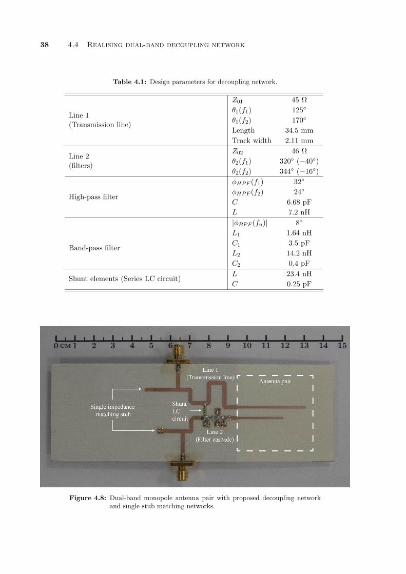
38 4.4 Realising dual-band decoupling network
Table 4.1: Design parameters for decoupling network.
Line 1(Transmission line)
Z01 45 Ω
θ1(f1) 125
θ1(f2) 170
Length 34.5 mm
Track width 2.11 mm
Line 2(filters)
Z02 46 Ω
θ2(f1) 320 (−40)
θ2(f2) 344 (−16)
High-pass filter
φHPF (f1) 32
φHPF (f2) 24
C 6.68 pF
L 7.2 nH
Band-pass filter
|φBPF (fn)| 8
L1 1.64 nH
C1 3.5 pF
L2 14.2 nH
C2 0.4 pF
Shunt elements (Series LC circuit)L 23.4 nH
C 0.25 pF
Figure 4.8: Dual-band monopole antenna pair with proposed decoupling networkand single stub matching networks.

Investigation of decoupling techniques 39
1.6 1.8 2.0 2.2 2.4 2.6
-30
-20
-10
0
f1
M
agni
tude
(dB
)
Frequency (GHz)
S11
S21
S22
f2
Figure 4.9: Measured scattering parameters of antenna pair with decoupling andmatching network.
Table 4.2: Performance of decoupling and matching network.
Without decoupling & matching networks
Return loss |S11(f1)| −12.8 dB
Return loss |S22(f2)| −13.1 dB
Port coupling |S21(f1)| −4.33 dB
Port coupling |S21(f2)| −6.25 dB
Antenna efficiency (f1) 57.3%
Antenna efficiency (f2) 71.2%
With decoupling & matching networks
Return loss |S11(f1)| −18.6 dB
Return loss |S22(f2)| −22.4 dB
Port coupling |S21(f1)| −22.6 dB
Port coupling |S21(f2)| −28.2 dB
Antenna efficiency (f1) 88.4%
Antenna efficiency (f2) 85.2%
4.5 Conclusion
Multiple techniques to reduce coupling between ports in a communication system were noted and
discussed. This chapter explores various forms of reactive decoupling networks to achieve port
isolation between identical antennas at a single frequency and dual frequencies. Furthermore, a
generalised reactive decoupling network to achieve port isolation between two distinct antennas
at two different frequencies was presented in Section 4.2. The proposed DMN was verified in
Section 4.3, with concluded findings published in [39].


CHAPTER
5
DESIGN OF ARRAY OF SUBARRAYS
5.1 Introduction . . . . . . . . . . . . . . . . . . . . . . . . . . . . . . . . . . . . . 41
5.2 Subarrays . . . . . . . . . . . . . . . . . . . . . . . . . . . . . . . . . . . . . . 42
5.3 Decoupling network . . . . . . . . . . . . . . . . . . . . . . . . . . . . . . . . 44
5.4 Power division . . . . . . . . . . . . . . . . . . . . . . . . . . . . . . . . . . . 54
5.5 Phase manipulation . . . . . . . . . . . . . . . . . . . . . . . . . . . . . . . . 58
5.6 Conclusion . . . . . . . . . . . . . . . . . . . . . . . . . . . . . . . . . . . . . 64
5.1 Introduction
This chapter reports the approach used to design an array of subarrays. To sufficiently verify
the concept, a minimum of three array element would be required. Each element in the array is
represented by a 3-element uniform circular subarray. The array of subarrays system consists of
multiple modular components that were designed and tested independently (except for decoup-
ling network). The architecture for an array of three subarrays is shown in Figure 5.1. Each
subarray employs three closely spaced vertical monopoles with a symmetric DMN to provide
port isolation between the element’s feed ports. Banks of independently controlled phase shifters
were utilised to individually control the radiation patterns of each subarray. Three-way power
dividers are employed to deliver equi-phase, equi-amplitude excitations to the phase shifter bank.
Finally, another bank of phase shifters and a power divider is used to provide control over the
array of subarrays factor.
The components of the system were manufactured on a number of substrates namely, Rogers
RT/duroid 5880 and Rogers RO4003C. The system was designed to operate at f0 = 2.7 GHz
and tested using a Rhode & Schwarz ZVL vector network analyser.
41

42 5.2 Subarrays
DM
ND
MN
DM
N
Subarray pattern control
Array of subarraysfactor control
SubarraysPhaseshifterPower
divider
Figure 5.1: Array architecture for 3-element array of subarrays.
5.2 Subarrays
Subarray centers were placed λ0/2 apart to minimise grating lobes and mutual coupling between
neighboring subarrays. To achieve λ/2 spacing, subarrays need to occupy and area less thanλ4 ×
λ4 . The employed subarrays were therefore miniturised to an interelement spacing of 0.15λ,
a distance significant enough to reduce the overall area of the subarray but retain enough dir-
ectivity. Standing monopoles were used as subarray elements due to their wide angle steering
capability and manufacturing simplicity. The monopoles were fabricated using 3 mm thick
cylindrical brass rods which were cut to the required length. The rods were tapered to a width
of 1.58 mm using a lathe to reduce the elements’ footprint and provide a consistent insertion
depth when fixing the monopoles to the substrate. Figure (5.2(a)) shows a cross sectional view
of a single standing monopole. A 1.6 mm hole is drilled through the substrate to mount the
monopole in the middle of an etched circle with a diameter of 4 mm on the ground plane to
prevent the antenna from shorting.
3 mm
23 mm
5 mm
Substrate
Ground
plane
Brass
monopole
1.58 mm
(a)
35 mm
Sub
stra
te b
ound
ry
18.23 mm
Feed ine
(b)
Figure 5.2: (a) Cross sectional view of standing monopole used in subarray. (b) Topview of subarray with feed lines on bottom layer of substrate.

Design of array of subarrays 43
The subarray was designed and fabricated on Rogers RT/duroid 5880 (t = 0.787mm, εr = 2.2
and tan δ = 0.0009). Subarray elements were excited using microstrip transmission lines etched
on the bottom of a hexagonal shaped substrate, as displayed in Figures 5.2(b). The measured
scattering parameters for the array displayed in Figure 5.3(a) include the effects of the feed
lines. Ensuring a true representation of the subarray scattering parameters becomes imperative
when designing a decoupling network. Due to the spatial constraint enforced on the subarray
size, the feed lines are eliminated to make room for a decoupling network. The removal of feed
lines in the scattering parameters was accomplished with the use of a TRL (thru, reflect, line)
de-embedding technique. A TRL calibration kit was fabricated (Figure 5.3(b)) and used to
de-embedded the subarray. The scattering parameters for a de-embedded subarray is illustrated
in Figure 5.4. There is strong coupling between subarray element with |S21| = |S31| = −8.0 dB
and |S11| = 7.5 dB at f0.
(a) (b)
Figure 5.3: (a) Bottom layer of subarray, showing microstrip feed lines. (b) TRLcalibration kit used to de-embed subarray.
1.4 1.6 1.8 2.0 2.2 2.4 2.6 2.8 3.0 3.2 3.4-20
-15
-10
-5
0
Mag
nitu
de (d
B)
Frequency (GHz)
S11
S21
S31
f0
Figure 5.4: Measured scattering parameters for de-embedded subarray.

44 5.3 Decoupling network
5.3 Decoupling network
A reactive decoupling network was used to create port isolation between the feed ports. The
design used to decouple the closely spaced subarray follows the principles discussed in Chapter 4.
Two variants of a decoupling network design which decouple and match a three element array
are discussed in this section. The decoupling network uses transmission line sections to trans-
form the impedance of the array elements and achieve port isolation. Variation in the network
topology will provide the option to position feed ports between array elements or inline with
array elements. Although both designs perform similarly, they are realised differently.
5.3.1 Impedance transforming network
The first segment of any decoupling network consists of an impedance transforming network as
noted in Chapter 4. A model of an ITC for a three element array is illustrated in Figure 5.5.
[Ya]
θ1 ,
Z01 θ
1 , Z
01
θ1 ,
Z01
i1′
i3′i
2 ′
1′V
1′
V2′ V
3′
2′ 3′
V1
V2
V3
1
2 3
Figure 5.5: Impedance transforming network for three element uniform circular ar-ray. [Ya] corresponds to the admittance matrix of the closely spacedsubarray elements.
The current distribution at the ports of a circularly symmetric 3-element array is given by
i1i2i3
=
Ya11 Ya
12 Ya12
Ya12 Ya
11 Ya12
Ya12 Ya
12 Ya11
V1
V2
V3
.
(5.1)

Design of array of subarrays 45
From transmission line theory, the voltage and current distributions at ports 1′, 2′ and 3′
coupled by transmission line section with a characteristic impedance Z01 and electrical length
θ1 are defined as
V′
1
V ′2V ′3
=
cos θ1 0 0
0 cos θ1 0
0 0 cos θ1
V1
V2
V3
+
j Z01 sin θ1 0 0
0 j Z01 sin θ1 0
0 0 j Z01 sin θ1
i1i2i3
,
(5.2)i′1
i′2i′3
=
cos θ1 0 0
0 cos θ1 0
0 0 cos θ1
i1i2i3
+
j Y01 sin θ1 0 0
0 j Y01 sin θ1 0
0 0 j Y01 sin θ1
V1
V2
V3
.
(5.3)
By substituting equation (5.1) into equation (5.2) and (5.3), the parameters at ports 1′, 2′ and 3′
are redefined as
V′
1
V ′2V ′3
=
cos θ1 0 0
0 cos θ1 0
0 0 cos θ1
V1
V2
V3
+
j Y01 sin θ1 0 0
0 j Y01 sin θ1 0
0 0 j Y01 sin θ1
Y′11 Y′12 Y′12
Y′12 Y′11 Y′12
Y′12 Y′12 Y′11
V1
V2
V3
,
(5.4)
i′1
i′2i′3
=
cos θ1 0 0
0 cos θ1 0
0 0 cos θ1
Ya
11 Ya12 Ya
12
Ya12 Ya
11 Ya12
Ya12 Ya
12 Ya11
V1
V2
V3
+
j Y01 sin θ1 0 0
0 j Y01 sin θ1 0
0 0 j Y01 sin θ1
V1
V2
V3
.
(5.5)

46 5.3 Decoupling network
Equations (5.4) and (5.5) can then be simplified to
V′
1
V ′2V ′3
=
cos θ1 + j Z01Ya11 sin θ1 Z01Ya
12 sin θ1 Z01Ya12 sin θ1
Z01Ya12 sin θ1 cos θ1 + j Z01Ya
11 sin θ1 Z01Ya12 sin θ1
Z01Ya12 sin θ1 Z01Ya
12 sin θ1 cos θ1 + j Z01Ya11 sin θ1
︸ ︷︷ ︸
A
V1
V2
V3
,
(5.6)i′1
i′2i′3
=
Ya11 cos θ1 + j Y01 sin θ1 Ya
12 cos θ1 Ya12 cos θ1
Z01Ya12 sin θ1 Ya
11 cos θ1 + j Y01 sin θ1 Ya12 cos θ1
Ya12 cos θ1 Ya
12 cos θ1 Ya11 cos θ1 + j Y01 sin θ1
︸ ︷︷ ︸
B
V1
V2
V3
.
(5.7)
Finally the admittance matrix at ports 1′, 2′ and 3′ is determined by
V1
V2
V3
= A−1
V′
1
V ′2V ′3
,
i′1
i′2i′3
= BA−1
V′
1
V ′2V ′3
,
Y′ = BA−1. (5.8)
Parameters Z01 and θ1 are calculated such that the real off-diagonal elements of Y′ equate to
zero.

Design of array of subarrays 47
5.3.2 Decoupling network with feed ports inline to array elements
The first variant of the decoupling network provides feed ports inline with array elements. A
model of this design can be seen in Figure 5.6.
[Ya]
i3′i
2 ′
2′
3′
θ 2 , Z 0
2
θ2 , Z
02
i1
a
i2
a
V2′′ V
3′′
i3
b
i1
b
2′′ 3′′i2′′ i
3′′
θ2 , Z02
θ1 , Z01
i1′
1′
V1′′i
1′′
θ 1 , Z 01
θ1 , Z01
i2
b i3
a
1′′
Figure 5.6: Three element decoupling network with feed ports inline to array ele-ments.
The current and voltage distributions at ports 1′′, 2′′ and 3′′ are defined by
V ′′1 = V ′1
V ′′2 = V ′2
V ′′3 = V ′3
(5.9)
i′′1 = i′1 + ia1 + ib1
i′′2 = i′2 + ia2 + ib2
i′′3 = i′3 + ia3 + ib3
(5.10)
Following the ITC network, the admittance matrix at ports 1′, 2′ and 3′ is found to be
i′1
i′2i′3
= Y′
V′
1
V ′2V ′3
,
(5.11)
With transmission line sections of a characteristic admittance Y02 and electrical length θ2 con-
nected between ports 1′, 2′ and 3′, the admittance matrix YTL of a transmission line section
(Figure 5.7) is defined as
YTL =
[−j Y02 cotθ j Y02 cosecθ
j Y02 cosecθ −j Y02 cotθ
].
(5.12)

48 5.3 Decoupling network
θ, Y0
i1
V2
V1
i2
1 2
Figure 5.7: Transmission line section.
For demonstration purposes, let
YTL =
[x y
y x
].
The current and voltage distribution at ports 1 and 2 of the transmission line are given by
[i1
i2
]=
[x y
y x
][V1
V2
].
(5.13)
From equations (5.12), (5.13) and (5.9) the current distributions between ports 1′, 2′ and 3′ is
determined by [ia1ia2
]=
[x y
y x
][V ′′1V ′′2
],[
ia2ia3
]=
[x y
y x
][V ′′2V ′′3
],[
ib3ib1
]=
[x y
y x
][V ′′3V ′′1
].
(5.14)
By substituting equations (5.11) and (5.14) into equation (5.10), the current distributions ob-
served at ports 1′′, 2′′ and 3′′ are determined by
i′′1
i′′2i′′3
=
Y′11 Y′12 Y′12
Y′12 Y′11 Y′12
Y′12 Y′12 Y′11
V′′
1
V ′′2V ′′3
+
x y 0
y x 0
0 y x
V′′
1
V ′′2V ′′3
,
+
x 0 y
0 x y
y 0 x
V′′
1
V ′′2V ′′3
,
=
Y′11 Y′12 Y′12
Y′12 Y′11 Y′12
Y′12 Y′12 Y′11
+
2x y y
y 2x y
y y 2x
V′′
1
V ′′2V ′′3
.
(5.15)

Design of array of subarrays 49
Thus the admittance matrix Y′′ at ports 1′′, 2′′ and 3′′ is provided by
Y′′ = Y′ +
2x y y
y 2x y
y y 2x
.
(5.16)
To achieve port isolation, the Y-parameters at ports 1′′, 2′′ and 3′′ need to satisfy the following
Y′′ =
G′11 + j(B′11 − Y02 cot(θ2)) 0 0
0 0 + j(B′12 − Y02 cosec(θ2)) 0
0 0 0 + j(B′12 − Y02 cosec(θ2))
.
(5.17)
The scattering parameters are then obtain using the following transformation
S′′ = (I− Z0Y′′) · (I + Z0Y
′′)−1. (5.18)
To decouple and match the subarray, parameters Z01, Z02, θ1 and θ2 are calculated such that
equation (5.31) is satisfied. There exists an infinite number of solutions to achieving port
isolation, therefore the best performing solution was obtained through the minimisation of a
cost function. The total power fed to a lossless closely spaced antenna array is the summation
of reflected power (|S′′11|2), coupled power (|S′′12|2) and radiated power (Prad). For a uniform
3-element UCA the input power is defined as
Pin = |S′′11|2 + |S′′12|2 + |S′′12|2 + Prad. (5.19)
Ideally, for an antenna array, Pin = Prad. From equation (5.19) the radiated power is given by
Prad = Pin − |S′′11|2 + 2|S′′12|2︸ ︷︷ ︸Cost function (f)
(5.20)
The cost function f is thus minimised via an optimisation routine to decouple and match the
closely spaced antenna array. Utilising this approach, a decoupling network that offers matched
ports without the use of a matching network can be computed. A DMN to the author’s know-
ledge not been implemented before.

50 5.3 Decoupling network
5.3.3 Decoupling network with feed ports between array elements
The second variant of the decoupling network places the feed ports between the antenna elements.
A model of this design is displayed in Figure 5.8.
i1′′
i2′′
i3′′
i1
a
i1
c
V1′′
i1
d i3
d
i3
c
i1
b
i2
b i2
a i2
ci2
d
i3
a
i3
b
V2′′
V3′′
i3′i
2 ′
2′
1′
3′θ2 /2
, Z02
θ2 /2
, Z02
θ 1 , Z 01
[Ya]θ1 , Z01
θ1 , Z
01
i1′
θ 2 /2, Z 0
2
θ 2 /2, Z 0
2
θ2 /2
, Z02
θ2 /2
, Z02
2′′
3′′1′′
Figure 5.8: Three element decoupling network with feed ports placed between arrayelements.
The current distribution at nodes 1′, 2′ and 3′ are considered to be
i′1 + id1 + id3 = 0,
i′2 + ib1 + ib2 = 0,
i′3 + id2 + ib3 = 0.
(5.21)
From equations (5.21) and (5.12) the current distribution for a transmission line section with
a characteristic admittance Y02 and electrical length θ/2 connected between nodes 1′′ and 2′ is
defined as,
[ia1ib2
]=
[−j Y02 cotθ2/2 j Y02 cosecθ2/2
j Y02 cosecθ2/2 −j Y02 cotθ2/2
][V ′′1V ′2
]=
[x y
y x
][V ′′1V ′2
],

Design of array of subarrays 51
Similarly, for other combinations between nodes 1′, 2′ and 3′ and 1′′, 2′′ and 3′′, respectively[ic1id1
]=
[x y
y x
][V ′′1V ′1
],[
ia2ib2
]=
[x y
y x
][V ′′2V ′2
],[
ic2id2
]=
[x y
y x
][V ′′2V ′3
],[
ia3ib3
]=
[x y
y x
][V ′′3V ′3
],[
ic3id3
]=
[x y
y x
][V ′′3V ′1
].
(5.22)
The current distributions at ports 1′′, 2′′, 3′′ are given by
i′′1 = ia1 + ic1,
i′′2 = ia2 + ic2,
i′′3 = ia3 + ic3.
(5.23)
From Ohm’s law the current distributions along nodes 1′, 2′, 3′ can also be defined asi′1
i′2i′3
=
Y′11 Y′12 Y′12
Y′12 Y′11 Y′12
Y′12 Y′12 Y′11
︸ ︷︷ ︸
Y′
V′
1
V ′2V ′3
.
(5.24)
Substituting equations (5.22) and (5.24) into (5.21) yields
Y′
V′
1
V ′2V ′3
+
2x 0 0
0 2x 0
0 0 2x
V′
1
V ′2V ′3
+
y 0 y
y y 0
0 y y
V′′
1
V ′′2V ′′3
=
0
0
0
.
(5.25)
This can be further simplified to
Y′ +
2x 0 0
0 2x 0
0 0 2x
︸ ︷︷ ︸
Y1
V′
1
V ′2V ′3
=
−y 0 −y−y −y 0
0 −y −y
︸ ︷︷ ︸
Y2
V′′
1
V ′′2V ′′3
.
(5.26)

52 5.3 Decoupling network
The voltage at nodes 1′, 2′ and 3′ relates to the voltages across feed ports 1′′, 2′′ and 3′′ through
the following
V′
1
V ′2V ′3
= Y2(Y′ + Y1)−1
V′′
1
V ′′2V ′′3
.
(5.27)
Similarly, substituting equation (5.22) into equation (5.23) yields
i′′1
i′′2i′′3
=
2x 0 0
0 2x 0
0 0 2x
︸ ︷︷ ︸
Y1
V′′
1
V ′′2V ′′3
+
y y 0
0 y y
y 0 y
︸ ︷︷ ︸
Y3
V′
1
V ′2V ′3
.
(5.28)
The current distributions at ports 1′′, 2′′ and 3′′ are obtained by substituting equation (5.27)
into equation (5.28)
i′′1
i′′2i′′3
=
Y1 + Y2 ×Y3(Y′ + Y1)−1︸ ︷︷ ︸Y′′
V′′
1
V ′′2V ′′3
.
(5.29)
The Y-parameters at the feed ports are thus defined by
Y′′ = Y1 + Y2 ×Y3(Y′ + Y1)−1. (5.30)
To achieve port isolation, parameters Z01, Z02, θ1 and θ2 are calculated such that the Y-
parameters at ports 1′′, 2′′ and 3′′ satisfy the following
Y′′ =
G′11 + j(B′11 − Y02 cot(θ2)) 0 0
0 0 + j(B′12 − Y02 cosec(θ2)) 0
0 0 0 + j(B′12 − Y02 cosec(θ2))
.
(5.31)
The cost function f = |S′′11 |2 + |S′′11 |2 is minimised through an optimisation routine to achieve
decoupled and matched ports.
5.3.4 Implementation of decoupling network
Two solutions were calculated for the three element UCA displayed in Section 5.2. The solutions
yielded the design parameters listed in Table 5.1

Design of array of subarrays 53
Table 5.1: Design parameters for decoupling network realisation.
Design from Section 5.3.2 Design from Section 5.3.3
Z01 = 33.261 Ω Z01 = 33.261 Ω
Z02 = 83.336 Ω Z02 = 57.256 Ω
θ1 = 97.27 θ1 = 65.927
θ2 = 65.927 θ2 = 118.187
Calculated |S21| = −26.3 dB Calculated |S21| = −23.3 dB
Calculated |S11| = −18.1 dB Calculated |S11| = −18.4 dB
Both designs result in isolated and matched ports without the need of a matching network.
Similarly the two solutions offered realisable design parameters, however given the array geo-
metry, the solutions’ electrical length θ2 was impractical to realise for both designs. Electrical
length θ2 can be easily extended with the addition of 360 (1λ), however the limited area of
the subarray rendered this option difficult but manageable. The design from Section 5.3.2 was
selected as the realisation of choice as it only requires θ2 = 425.927 of electrical length as oppose
to θ2 = 478.187.
A model of the subarray can be seen in Figure 5.9(a) where the decoupled antenna array was
fabricated on Rogers RT/duroid 5880. The design is displayed in Figure 5.9(b) and is etched
on the bottom side of the substrate. Furthermore the transmission line sections between the
subarray’s feed ports were meandered to fit in the available area. The decoupling network was
measured and its performance illustrated in Figure 5.10.
3-element
subarray
Decoupling
network
(a)
Sub
stra
te b
ound
ry
(b)
Figure 5.9: (a) Exploded view of subarray with the addition of decoupling networkon the bottom layer. (b) Top view of decoupling network.
The decoupling network provided excellent port isolation and satisfactory return loss for all three
ports. Note that the decoupling network provided port isolation without the use of a matching
network.

54 5.4 Power division
2.2 2.4 2.6 2.8 3.0 3.2 3.4-30
-25
-20
-15
-10
-5
0
Mag
nitu
de (d
B)
Frequency (GHz)
S11
S12
f0
Figure 5.10: Measured scattering parameters for subarray with decoupling network.
5.4 Power division
5.4.1 Design
A 3-way distributed, equi-phase, equi-amplitude power divider is required to deliver excitation
signals to each subarray element. The employed power divider adopts the design of a three
way Bagley polygon divider (Figure 5.11). As is, the Bangley power divider can produce equi-
amplitude but not equi-phase outputs (port 4 leads ports 2 and 3 by 90) and requires at least
a minimum footprint ofλ
2× λ
2to fabricate.
λ/2
λ/4
2
3Z0
1
2 3
4
Figure 5.11: 3-way Bagley polygon power divider.
Demonstrated in [40–42] are methods of miniaturising transmission line sections by periodically
loading shorter transmission line sections in shunt. A conventional transmission line can be
represented by an infinite number of LC cells (Figure 5.12(a)). The number of cells used dictate,

Design of array of subarrays 55
the characteristic impedance of a transmission line section and can be expressed in terms of the
following
Z0TL =
√L
C.
Furthermore, the phase velocity of the wave traveling through the line can be found by
vpTL =1√LC
.
θTL
Z0TL
,
C
L
(a)
=Z0TL
d
l
Z0TL
Z0Stub
Cp
d
(b)
Figure 5.12: (a) Representation of conventional transmission using LC cells. (b)Equivalent circuits of loaded transmission line section using lumpedand distributed elements.
λ/4Z0 ,
Zb ,θ
bZ
b ,θ
bZ
b ,θ
b
Za ,θ
aZ
a ,θ
a
Figure 5.13: Equivalent miniaturisedcoupling network for λ/4transmission line section.
In this section, the minaturisation of a transmission
line section through reactive loading is considered. An
example of such circuit can be seen in Figure (5.12(b)),
where a conventional transmission line section is loaded
using open circuited stubs or lumped capacitors. The
miniaturised transmission line is reduced in physical
length and is known as an artificial transmission line.
when the periodic shunt capacitance is spaced equally
at intervals, d m apart (d << λ0), the periodic struc-
ture acts like a conventional transmission line. The
characteristic impedance and phase velocity of the ar-
tificial transmission line are given by [40]

56 5.4 Power division
Z0ATL =
√L
C +Cp
d
,
vpATL =1√
L(C +
Cp
d
) .(5.32)
It can be deduced from equation (5.32) that capacitive loading of a conventional transmission
line lowers the effective characteristic impedance and phase velocity. Attaining a lower phase
velocity means that a physically shorter artificial transmission line section can be used to yield
a similar electrical length to a longer conventional transmission line. By extension, a Bangley
power divider [42] can be miniaturised by replacing its conventional transmission line sections
with artifical transmission lines which will provide the same electrical length and character-
istic impedance as conventional lines. An example of this configuration can be seen in Figure
5.13, where a conventional λ/4 transmission line section with the a characteristic impedance
Z0 provides the same input impedance and electrical length as a physically shorter (θa < λ/8),
capacitance loaded, transmission line structure. Note that neither the open-circuited stubs nor
the coupling transmission lines sections retains the characteristic impedance of Z0.
5.4.2 Implementation
Design parameters Za, Zb , θa and θb are determined from the following equations [42]
C2a + 3CaTbSaZaZbS
2a − S2
aT2b Za
2Z2b = 0, (5.33)
Z0 = SaZa(2Ca+ TbSaZaZb), (5.34)
where Ca = cos(θa), Sb = sin(θa) and Tb = tan (θb). The electrical lengths θa and θb are selected
to determine the degree of miniaturisation prior to calculating the required impedances from
equations (5.33) and (5.34). The design parameters for a 3-way power divider were calculated
and are listed in Table 5.2. Coupling transmission line sections with an electrical length of θa
were curved to improve the spatial efficiency of microstrip structure. Equi-phase outputs from
the power divider were achieved with the addition of 90 transmission line sections to ports 2
and 3.
Table 5.2: Design parameters for miniturised transmission line section.
Za Za θa θb139.3 Ω 44.5 Ω 22.5 32.7
The power divider was fabricated on Rogers RO4003C laminate (t = 0.813mm, εr = 3.38 and
tan δ = 0.0021), where it occupies an area of 49.4 mm × 44.8 mm (Figure 5.14). The measured
scattering parameters and phase response are illustrated in Figures 5.15 and 5.16, respectively.

Design of array of subarrays 57
(a)
1
2
3
4
49.4 mm
44.8 mm
(b)
Figure 5.14: (a) Fabricated 3-way microstrip Bagley power divider. (b) Artwork for3-way Bagley power divider.
The power divider performed as calculated with an insertion loss of −24.2 dB and equi-amplitude
and equi-phase outputs at ports 2, 3 and 4. The achieved average output was −5 dB with respect
to the input. This represents an error of 0.23 dB compared to the ideal output value of −4.77
dB, which ascribed to fabrication inaccuracy.
Table 5.3: Performance of 3-way power divider.
S11(port 1) S21(port 2) S31(port 3) S41(port 4)
Magnitude (dB) −24.2 −5.02 −5.04 −4.93
Phase (degrees) −137.6 −65.7 −65.7 −68.07
1.4 1.6 1.8 2.0 2.2 2.4 2.6 2.8 3.0 3.2 3.4-8
-7
-6
-5
-4
-3
f0
Mag
nitu
de (d
B)
Frequency (GHz)
S21
S41
S31
-4.77 dB
Figure 5.15: Measured scattering parameters for 3-way miniaturised power divider.

58 5.5 Phase manipulation
1.4 1.6 1.8 2.0 2.2 2.4 2.6 2.8 3.0 3.2 3.4
-180
-135
-90
-45
0
45
90
135
180
Phas
e (d
egre
es)
Frequency (GHz)
S31
S21
S41
f0
Figure 5.16: Measured phase response for 3-way miniaturised power divider.
5.5 Phase manipulation
The array factor for both array of subarrays and individual subarrays are manipulated using
phase shifters. Beam steering techniques utilise components that rely on varying a bias voltage
to achieve an infinite number of possible phase shifts within a given range. Examples of struc-
tures that could provide such a capability are reflective phase shifters [43] and analog packaged
integrated circuits such as [44]. A simplified approach to beam steering is beam switching via
components that rely on Boolean logic circuitry to provide preselected phase shift values. Beam
switching generally results in lower insertion loss than beam steering but results in phase errors
due to the finite bit resolution used to realise phase shifts. Examples of structure that could
provide such a capability include switched loaded or conventional transmission line sections [27],
Butler matrix networks [45] and digital packed integrated circuits [46].
5.5.1 Design
Switched transmission line sections were chosen to accomplish beam switching for individual
subarrays and array of subarrays to due to their simple implementation. The total range of
phase shifts provided by switched transmission lines do not require to be 360. Beam switching
can be successfully implemented by considering the relative phase shift between array elements.
By considering the excitations required to achieve maximum directivity at direction φ0, it was
determined that the switched line phase shifters required three bits to realise maximum directiv-
ity at −180 < φ0 < +180 at 30 increments. This was verified using EM simulating package
CST.
Figure ?? shows the layout for a switched line phase shifter used to control the subarray and
array factor alongside their respective reference lines. The reference line is used to excite a single
element while two switched line phase shifters vary the phase excitation fed to the remaining

Design of array of subarrays 59
two elements. The relative electrical length θR for each switched line in respect to the reference
line was considered to allow for the widest range of possible relative phase shifts.
5.5.2 Implementation
A radio frequency (RF) single pole, double throw (SPDT) switch HMC545E from Hittite was
employed to navigate the excitation signal between different transmission line sections. The
switch is controlled using +5.0 V and +0.2 V DC signals to represent the two Boolean input
states (0 and 1) required. The switch’s performance was individually tested using an evaluation
circuit displayed in platform Figure 5.17(a). A switching logic circuit was designed and fabricated
as seen in 5.17(b). The circuit makes use of a hex inverter integrated circuit (74HC04), DIP
switches and pull up resistors. The measured magnitude and phase response for the switch are
displayed alongside the manufacturer’s supplied results in Figures 5.18 and 5.19. Discrepancies
between the two sets are moderate, showing an increased insertion loss and 15 of phase error.
The 545E switch proved challenging to install, due to its sensitivity to heat with a reflow temper-
ature of 260C, much lower than the typical 340C offered by soldering irons. Ideally, the switch
should have been mounted on the board using solder paste and a heating oven or a fine-tipped,
low temperature soldering iron. The performance of the switch also suffers if its ground pin is
not soldered directly to a via or a ground pad. These errors were verified by fabricating and
testing multiple unique evaluation boards mounted with 545E switches, all to which resulted in
performance errors due to the noted reasons. Although it displayed inconsistent performance
the 545E switches were still installed on the switched line phase shifters due time constraints
associated with this project.
A combination of the possible relative phase shifts contributed by the subarray and array
switched line phase shifters are listed in Tables 5.4 and 5.5, respectively.
Table 5.4: Electrical lengths contributedby subarray phase shifter fordifferent bit combinations
Total θR Bit 3 Bit 2 Bit 1
60 0 0 0
90 0 0 1
150 0 1 0
180 0 1 1
210 1 0 0
240 1 0 1
300 1 1 0
330 1 1 1
Table 5.5: Electrical lengths contributedby array phase shifter for dif-ferent bit combinations
Total θR Bit 3 Bit 2 Bit 1
90 0 0 0
150 0 0 1
180 0 1 0
240 0 1 1
210 1 0 0
270 1 0 1
300 1 1 0
360 1 1 1

60 5.5 Phase manipulation
Ground
Logic input 1
Logic input 0
θR= 0º
Reference line θR= 60º
θR= 90º
θR= 30º
θR= 150º
SPDT
switch
Subarray
switched
line
phaseshifter
Array
switched
line
phaseshifter
θR= 90º
θR= 60º
θR= 120º
Reference line θR= 90º
64 .3 mm
28
.4 m
m

Design of array of subarrays 61
(a) (b)
Figure 5.17: (a) SPDT 545E Hittite switch. (b) Control Boolean logic circuit usingDIP switches.
1.4 1.6 1.8 2.0 2.2 2.4 2.6 2.8 3.0 3.2 3.4
-4
-3
-2
-1
0
Mag
nitu
de (d
B)
Frequency (GHz)
Manufactuer's S21
Measured S21
f0
Figure 5.18: Performance of SPDT 545E Hittite switch.
1.4 1.6 1.8 2.0 2.2 2.4 2.6 2.8 3.0 3.2 3.4
-180
-135
-90
-45
0
45
90
135
180
Phas
e (d
egre
es)
Frequency (GHz)
Manufactuer's S21
Measured S21
f0
Figure 5.19: Phase response of SPDT 545E Hittite switch.

62 5.5 Phase manipulation
The switched phase shifters were designed and manufactured on Rogers RO4003C substrate,
545E switches were mounted onto the boards via a variable temperature soldering iron set to
220C. Displayed in Figures 5.20 and 5.21 are subarray and array switched line phase shifters,
respectively. The measured phase response of the two phase shifters is listed in Tables 5.6
and 5.7, respectively. Furthermore, the insertion loss scattering parameters associated with the
different bit combinations for both subarray and array switched lines is shown in Figures 5.22 and
5.23. Note that the power divider has been de-embeded. There appears to be significant error
between the expected and measured phase shifts provided by the switched line phase shifters.
Inconsistency in the performance of the 545E switch is considered to be the prime source of this
error.
Figure 5.20: Switched line subarray phase shifter with 3-way power divider.
Figure 5.21: Switched line array phase shifter with 3-way power divider.

Design of array of subarrays 63
Table 5.6: Phase response of subarray switched line phase shifter.
Expected θR 60 90 150 180 210 240 300 330
Measured θR 67.0 101.8 170.4 203.8 225.0 261.9 330.2 364.5
Table 5.7: Phase response of array switched line phase shifter.
Expected θR 90 150 180 210 240 270 300 360
Measured θR 96.4 162.7 195.1 229.0 258.2 292.5 323.8 386.4
2.2 2.4 2.6 2.8 3.0 3.2 3.4-20
-15
-10
-5
0
S21
: 0 Bits HIGH S
21 : 1 Bits HIGH
S21
: 2 Bits HIGH S
21 : 3 Bits HIGH
Mag
nitu
de (d
B)
Frequency (GHz)
f0
Figure 5.22: Insertion loss for subarray switched lines phase shifter for differentbinary bit combinations.
2.2 2.4 2.6 2.8 3.0 3.2 3.4-25
-20
-15
-10
-5
0S
21 : 0 Bits HIGH
S21
: 1 Bits HIGH S
21 : 2 Bits HIGH
S21
: 3 Bits HIGH
Mag
nitu
de (d
B)
Frequency (GHz)
f0
Figure 5.23: Insertion loss for array switched lines phase shifter for different binarybit combinations.

64 5.6 Conclusion
5.6 Conclusion
The approach to designing an array of subarray requires the realisation of a compact subarray.
However reduction in interelement results in aggrevated mutual coupling between array elements.
This chapter described two variations of a decoupling networks for a 3-element uniform circular
array using only transmission lines sections. The two decoupling networks preform similarly, but
are realised differently. The networks provided matched ports without the need of a matching
network, an approach to the author’s best knowledge never implemented before.
A 3-way equi-phase, equi-amplitude power divider was designed and fabricated to ensure equal
power distribution to all array and subarray elements. Similarly, a bank of switched line phase
shifters was utilised to vary the phase excitation to array and subarray elements in order to
beam switch the maximum directivity to a given angle φ0.
There were moderate discrepancies between the expected and measured phase shifts from the
output of the switched line phase shifters. It was concluded that such errors were due to the
inconsistency of the 545E switch used in the proposed design.

CHAPTER
6
OPERATING AN ARRAY OF SUBARRAYS
6.1 Implementation . . . . . . . . . . . . . . . . . . . . . . . . . . . . . . . . . . . 65
6.2 Results . . . . . . . . . . . . . . . . . . . . . . . . . . . . . . . . . . . . . . . . 68
The feed excitation vector used in an antenna array relies exclusively on the desired outcome
of the array. There exists a diverse range of applications that utilise antenna arrays namely
to achieve beam steerability, higher directivity and/or higher beam resolution. Increasing the
number of array elements enhances the array’s capabilities but increases the complexity of the
feed network. The concept of array of subarrays offers a solution to said problem. Although
the number of feed networks needed for an N−subarray array are N − 1 folds more than a
conventional array.
6.1 Implementation
To ensure 0.5λ0 separation between the centers of subarrays a Perspex chassis was laser cut
with apertures underneath each subarray to ensure that the effective dielectric of microstrip
transmission lines remain unchanged (Figure 6.1(a)). Additional holes were cut out for nylon
bolts to secure the subarray board in place (Figure 6.1(b)). Rigid shielded coax cables were
soldered to decoupled and matched subarray ports and are passed through the bottom of the
chassis via an opening where they will be connected to a bank of phase shifters (Figure 6.1(d)).
The array of subarrays can be considered to be an array with adaptive array elements. Desiring a
maximum in direction φ0 is accomplished by steering subarray factors to φ0 followed by steering
the array factor to φ0. Conventional formulation used to calculate the excitation vector for
maximum directivity at φ0 can no longer be found via Section 2.4.2. This is due to the inclusion
of the decoupling network which alters the current distribution on the surface of the antennas.
65

66 6.1 Implementation
(a) (b)
(c) (d)
Figure 6.1: (a) Top view of array of 3-subarrays. (b) Side view of array of 3-subarrays. (c) Subarrays fed via rigid coax cable. (d) Coax cableconnected to decoupled and matched subarray ports.
The excitation vector for a maximum at φ0 was determined through the use of the EM simulating
package, CST. An optimisation procedure was executed to determine the required excitation
vector at increments of 30 across the φ−plane. Obtained values were quantised to the nearest
bit value available in the switched line phase shifter. A model representing the array of subarray
in CST can be seen in Figures 6.2. The excitation phase offsets (φ1 and φ2) required to achieve
maximum directivity are listed for array and subarrays in Tables 6.1 and 6.2, respectively. Note,
the tabulated results are obtained via simulation using CST.

Operating an array of subarrays 67
(a) (b)
(c) (d)
Figure 6.2: CST models for array of 3-subarray. (a) Bottom view (b) Top view. (c)Radiation pattern of subarray with maximum beam at φ0 (d) Radiationpattern of array of 3-subarrays with maximum beam at φ0.

68 6.2 Results
Table 6.1: Phase shifts for steeringsubarray maximum to φ0
φ0 φ1 φ2
30 300 60
60 90 180
90 90 150
120 90 60
150 60 330
180 240 330
210 330 240
240 330 240
270 300 240
300 240 330
330 240 330
360 300 60
Table 6.2: Phase shifts for steeringsubarray maximum to φ0
φ0 φ1 φ2
30 360 300
60 90 240
90 90 90
120 150 150
150 360 300
180 240 300
210 90 360
240 300 360
270 360 90
300 90 90
330 90 180
360 90 360
6.2 Results
The radiation pattern for omni-direction steerability of a subarray has been captured and illus-
trated in Figure 6.3 and 6.4. Similarly the radiation pattern for an array of subarrays has been
captured for maximum directivity at different increments of φ0. This was achieved by aligning
the maximum directivity of the subarray factor with that of the array factor (Figure 6.5 and
6.6).
A clear improvement in directivity is observed when steering the main beam of the array of
subarrays across the φ plane. A list of all the registered directivity are tabulated in Table 6.3.
Table 6.3: Maximum direcitivy for an array of 3-subarray at 30 increments in φplane.
Angle 30 60 90 120 150 180 210 240 270 300 330 360
Directivity (dB) 6.42 5.55 4.89 4.79 5.13 2.84 3.16 2.60 3.05 5.67 5.12 5.01
Angles 180, 210 and 240 provide negative or no improvements when compared with a conven-
tional 3-element monopole array which has a maximum directivity of 3 dB. Lack of perform-
ance at the mentioned angles is contributed by a quantisation error associated with digitally
controlling the phase shifters. Note, the tabulated results are obtained via simulation using
CST.

Operating an array of subarrays 69
ϕ, θ = 90º ϕ, θ = 90º
ϕ, θ = 90ºϕ, θ = 90º
ϕ, θ = 90ºϕ, θ = 90º
Dir
ecti
vit
y (
dB
)
Dir
ecti
vit
y (
dB
)D
irec
tiv
ity
(d
B)
Dir
ecti
vit
y (
dB
)
Dir
ecti
vit
y (
dB
)
Dir
ecti
vit
y (
dB
)
Figure 6.3: Normalised radiation pattern of 3-element subarray for maximum dir-ectivity at angles φ0 = 0 to 150. Blue line indicating direction ofmaximum directivity.

70 6.2 ResultsD
irec
tivit
y (
dB
)D
irec
tivit
y (
dB
)D
irec
tivit
y (
dB
)
Dir
ecti
vit
y (
dB
)D
irec
tivit
y (
dB
)D
irec
tivit
y (
dB
)
ϕ, θ = 90º
ϕ, θ = 90º
ϕ, θ = 90º
ϕ, θ = 90º
ϕ, θ = 90º
ϕ, θ = 90º
Figure 6.4: Normalised radiation pattern of 3-element subarray for maximum dir-ectivity at angles φ0 = 180 to 330. Blue line indicating direction ofmaximum directivity.

Operating an array of subarrays 71
Dir
ecti
vit
y (
dB
)D
irec
tiv
ity
(d
B)
Dir
ecti
vit
y (
dB
)
Dir
ecti
vit
y (
dB
)D
irec
tiv
ity
(d
B)
Dir
ecti
vit
y (
dB
)
ϕ, θ = 90º ϕ, θ = 90º
ϕ, θ = 90º
ϕ, θ = 90ºϕ, θ = 90º
ϕ, θ = 90º
Figure 6.5: Normalised radiation pattern of array of subarrays with maximum atangles φ0 = 0 to 150. Blue line indicating direction of maximumdirectivity.

72 6.2 ResultsD
irec
tivit
y (
dB
)D
irec
tivit
y (
dB
)D
irec
tivit
y (
dB
)
Dir
ecti
vit
y (
dB
)D
irec
tivit
y (
dB
)D
irec
tivit
y (
dB
)
ϕ, θ = 90º
ϕ, θ = 90º
ϕ, θ = 90º
ϕ, θ = 90º
ϕ, θ = 90º
ϕ, θ = 90º
Figure 6.6: Normalised radiation pattern of array of subarrays with maximum atangles φ0 = 180 to 330. Blue line indicating direction of maximumdirectivity.

CHAPTER
7
METHODOLOGY OF FABRICATING PRINTED
CIRCUIT BOARDS
7.1 Objective . . . . . . . . . . . . . . . . . . . . . . . . . . . . . . . . . . . . . . 73
7.2 Artwork generation . . . . . . . . . . . . . . . . . . . . . . . . . . . . . . . . . 73
7.3 Milling . . . . . . . . . . . . . . . . . . . . . . . . . . . . . . . . . . . . . . . . 74
7.4 Laminate printing . . . . . . . . . . . . . . . . . . . . . . . . . . . . . . . . . 77
7.5 Etching . . . . . . . . . . . . . . . . . . . . . . . . . . . . . . . . . . . . . . . 85
7.6 Results . . . . . . . . . . . . . . . . . . . . . . . . . . . . . . . . . . . . . . . . 87
7.7 Conclusion . . . . . . . . . . . . . . . . . . . . . . . . . . . . . . . . . . . . . 91
7.1 Objective
The process of fabricating high quality double-sided printed circuit boards (PCBs) is well known
and documented. Detailed literature [47] of the procedure can be found as early as 1983. The
development of more capable machinery has introduced alternative methods to the fabrication
process [48]. This chapter discusses the implementation of some of those methods using low-cost,
widely available equipment and materials. The aim is to establish the capability to fabricate
PCBs in-house at minimal cost while reducing turnover time. A series of experiments were
conducted to identify an efficient and consistent method of fabricating PCBs on a variety of
laminates. The designs used in this chapter are independent of the thesis topic and are selected
to demonstrate the respective techniques and/or method.
7.2 Artwork generation
Artwork refers to the visual pattern or design used to indicate the size of the board, position
of any conducting cladding and position of any required components. In the early stages of
73

74 7.3 Milling
PCB manufacturing, designers relied on hand drawn artwork. This was acceptable for DC/low
frequency applications but the performance of microwave circuits relied heavily on the designers
accuracy and consistency. Even with highly skilled freehand designers the lack of precision often
caused unwanted parasitic effects. Freehand PCBs quickly became obsolete with the advent of
computer-aided design (CAD) software. There are many PCB CAD software available in the
public domain, all of which use the de facto digital artwork format called Gerber.
Gerber files are based on a vector language which uses polygons to represent circuit designs.
The simplicity of the Gerber format encouraged cross software compatibility between PCB CAD
software and manufacturers. An example of Gerber representation can be seen in Figure 7.1.
(a) (b)
Figure 7.1: (a) 3-D CAD drawing of branchline coupler, modelled via CST. (b)Equivalent Gerber representation of branchline coupler via vector poly-gons.
7.3 Milling
Precision milling machines enabled a large portion of industry professionals and enthusiasts to
begin prototyping PCBs with turnover times of 5 to 30 minutes depending on the boards dimen-
sions. Control software reads in Gerber format files and consequently dictates the movement of
a milling tool (or more commonly the platform hosting the laminate) in order to fabricate the
user’s design. Coplanar circuit designs tend to be preferred due to the minimal effort required
to fabricate them. Unlike microstrip circuit designs, only an isolation gap is required between
the conducting transmission line and the ground plane. This milling approach reduces turnover
time and prolongs the milling tool’s life span. An illustration of this concept can be seen in
Figure 7.2.
The tool employed by the milling process is traditionally forged from tungsten carbide or steel
and comes in a variety of shapes. However, regardless of the milling tool’s physical characterist-
ics, the resultant material surface will often become non-uniform due to scalloping. Scalloping
occurs when a milling tool steps over in a single spatial axis and performs several orthogonal cuts
to the step. This results in small cusps in the material being operated on, as seen in Figure 7.3.

Methodology of fabricating printed circuit boards 75
Ground plane
Microstrip CoplanarConductor
MMB 2014
Figure 7.2: Structure of a microstrip transmission line and a coplanar transmissionline.
Reduction in step over distance will minimise the scallop height but will increase the number
of cusps found on the surface of the worked material. Furthermore milling increases the surface
roughness of the conductor in the proximity to a scalloped region. Models of transmission lines
with varying roughness have been analysed in [49,50]. An empirical formula was developed in [49]
to calculate the total attenuation coefficient with surface roughness. The total attenuation is
determined by
α′c = αc ·KSR, (7.1)
where α′c is total attenuation, and αc is the attenuation coefficient for a smooth conductor. The
effects of frequency dependent loss KSR is calculated by
KSR = 1 +2
πarctan[1.4(
∆
δ)2] (7.2)
where ∆ is the surface roughness and δ is the skin depth. The value of KSR is equal to 1 at DC.
Conversely KSR approaches 2 as frequency increases; suggesting transmission losses of up 3 dB
per meter.
ScallopHeight
ScallopDistance
Millingtool
Substrate
Conductor
Surface roughness
MMB 2014
Figure 7.3: Milling tool operating on a laminate. Included are the effects of scal-loping and conductor surface roughness.

76 7.3 Milling
(a) (b)
(c) (d)
Figure 7.4: (a) Image of ProtoMat S103 by LPKF Laser & Electronics. (b) Milledcoplanar design on FR-4 substrate. (c-d) Milled microstrip design onRogers RT/duroid 5880 & FR-4 substrates, respectively. Cusps visibleon the surface of both laminate.
The milling machine’s fabricating capabilities were put to the test by microstrip and coplanar
designs. The machine used was the ProtoMat S103 by LPKF Laser & Electronics (Figure
7.4(a)). Some notable specifications include an operating resolution of 0.5 µm in the XY–plane,
repeatability of ±1 µm and a front-to-back alignment precision of 20 µm. The ProtoMat S103
lacked resolution when operating in the Z–plane (depth) [51]. This often caused the milling of
significant amount of substrate from the laminate. The ProtoMat S103 met all specifications set
for coplanar designs fabricated on fibreglass-resin laminate (FR-4) laminates (Figure 7.4(b)).
Milling microstrip designs did not yield results as satisfactory as coplanar designs. Two mi-
crostrip designs were millied on Rogers RT/duroid 5880 and FR-4 laminates sized 30 × 65 mm
with a thickness of 1.575 mm (62 mil) and 35 µm of copper cladding. The extensive milling
required to realise the design populated the boards with the affects of scalloping on both PCBs,
albeit less on FR-4. Milled Rogers RT/duroid 5880 and FR-4 laminates can be seen in Figures
7.4(c) and 7.4(d), respectively.

Methodology of fabricating printed circuit boards 77
7.4 Laminate printing
An alternative method to fabricating PCBs is laminate printing followed by chemical etching.
The process of laminate printing introduces a protective layer on top of the conductor cladding
prior to submerging the laminate in an oxidising (etching) solution. Consequently the protected
cladding will remain, whilst exposed regions of conductor cladding displace into the solution.
Both coplanar and microstrip PCBs can be fabricated using this method, with the later being
vastly more popular. This section discusses three viable methods of printing on laminates.
7.4.1 Photolithography
Photolithography utilises ultraviolet (UV) light and a photosensitive polymer synthesised from
butyl ethanoate to print on laminates. The process is usually conducted in a “clean room” where
dust levels are minimal and ambient light levels are optimised to not pollute the photoresist.
Although clean rooms were not available at the time of experimentation, precautions were taken
to minimise the effects of dust and ambient light in the working environment. A visual repres-
entation of photolithography is shown in Figure 7.5.
The process begins by cleaning the cladding on the laminate with isopropyl alcohol or acetone
to eliminate dust or other forms of impurities. Once the laminate has dried the photosensitive
polymer is uniformly applied to the cladding. Ideally, layer uniformity is maintained by fixing
the laminate onto a centrifugal device while the the photosensitive polymer is sprayed on using
a compressed canister. The photoresist coated laminate is then cured at 60C for 20 minutes or
room temperature for 24 hours. Alternatively, a dry photosensitive film can be used to easily
obtain a uniform layer. The uniformity of the photoresist layer greatly dictates the quality of
the etched PCB. A centrifugal machine was not available during the experimentation process
nor was dry photoresist film which can be rolled on the laminate. Instead, the photoresist was
applied freehand using a compressed canister.
The photomask was prepared in accordance to the type of the photoresist used. The majority of
available photoresists are positive therefore the artwork used in the mask should represent the
conductor with black or filled rather than clear. Due to the involvement of UV light the mask
is produced on transparency paper to provide a greater margin of contrast. The photomask
was aligned over the cured laminate and together are exposed to UV light for a duration of 15
to 35 seconds (The UV light source will be discussed in further details in Section 7.4.1.1). It
was important to ensure the photomask sits flush against the laminate to avoid artifacts due
to shadowing. When exposed to UV light the photoresist polymer becomes soluble in alkaline
solutions (developing solutions) such as sodium hydroxide or sodium metasilicate pentahydrate.
The developer of choice was sodium hydroxide, a colourless solution which takes the colour of the
photoresist polymer when used. Four laminates were methodically cured, exposed and developed
whilst exclusively varying developing time. The laminates were submerged in developing solution

78 7.4 Laminate printing
Photoresist
Glass
Photomask
① Prepare laminate ② Apply photoresist
③ Align photomask ④ Expose to UV light
⑤ Develop/dissolve exposed photoresist
⑥ Inspect print for etching
ExposedPhotoresist
Developing Agent
MMB 2014
Figure 7.5: Printing on laminates using photolithography.

Methodology of fabricating printed circuit boards 79
Figure 7.6: Effects of developing duration using sodium hydroxide solution for dur-ations of 75, 60 and 45 seconds, respectively (left to right).
for intervals of 30, 45, 60 and 75 seconds. Upon inspection it appeared that 60 seconds yielded
the best contrast compared to other test samples. Figure 7.6 illustrates the effects of limited and
excessive development times. Developing repeatability using sodium hydroxide solution was very
poor. The solution’s performance varied greatly due to solution’s sensitivity to temperature and
aqueous concentration. Due to these inconsistencies, the use of sodium metasilicate pentahydrate
is preferred when developing durations printed designs.
The results obtained using photolithography printing followed by etching were not satisfactory.
The process is recognised as the de facto method for fabricating PCB and has been proven to
produce excellent results. Discrepancies between Gerber design and the in-house final product
can be accounted by the following :
1. The application of photoresist layer on the laminates was not uniform due to the lack of
a centrifugal machine or dry photoresist film.
2. The use of sodium hydroxide as the developing solution caused a large margin of uncer-
tainty to define a methodical process of development. In hindsight, sodium metasilicate
pentahydrate would have been a superior choice.
7.4.1.1 UV exposure equipment
A custom UV exposure box was built using medium-density fibreboard (MDF). Six 8W, T8
tubes alongside six 9W inductive ballasts were used to provide a source of UV light in the
exposure box (Figure 7.7). A lighting configuration for a single UV tube is illustrated in Figure
7.8.

80 7.4 Laminate printing
Figure 7.7: Exposure box with raised lighting platform. Inductive ballasts preparedto be installed beneath platform.
A 1.2 mm of clear glass was fixed at the aperture of the box to hold the laminate in place.
The tubes were spaced such that uniform illumination is provided at the box’s aperture. UV-A,
commonly refered to as black light is needed for the photoresist process. UV-A has a wavelength
range of 315–400 nm. The required UV dosage was not specified by the manufacturer, but an
estimation of 250–700 mJ/cm2 would suffice for the majority of butyl ethanoate photoresists [52].
The dosage of UV radiation delivered to a unit area is given by
Dosage = Intensity × Time, (7.3)
S
Inductiveballast240 V
60 Hz
Starter
Fluorescent tube
Figure 7.8: Lighting schematic for a single UV florescent tube.

Methodology of fabricating printed circuit boards 81
where
Intensity =Power
Area. (7.4)
A mirror was placed behind the tubes and reflective film was placed in the inner lining of the
box to increase exposure intensity in the direction of interest. The tubes were placed a distance
of 22 cm away from the box’s aperture, as seen in Figure 7.9. For simplicity, the tubes were
considered to be isotropic radiators, meaning they radiate equally in a sphere. The area of
radiation is defined as
Area of sphere = 4πR2,
where R = distance from illumination source.
Furthermore, the intensity at the aperture of the box can be estimated using equation 7.4. Power
in the direction of interest has been numerically doubled to account for reflective materials in
the box’s cavity. The intensity is thus estimated by
intensity =Power
Area=
2× 6× (8000 mW)
4π × (22 cm)2= 15.78 mW/cm2.
The time required to deliver the required dosage of UV-A radiation is therefore between
Maximum time =Maximum dosage
Intensity=
700 mJ
15.78 mW/cm2 = 44.35 seconds,
and
Minimum time =Minimum dosage
Intensity=
250 mJ
15.78 mW/cm2 = 15.84 seconds.
(a) (b)
Figure 7.9: (a) Inside cavity of exposure box. (b) Operating exposure box withraised lighting platform.

82 7.4 Laminate printing
The exposure box preformed well, taking ∼45 seconds to optimally expose coated laminates.
The implementation of a digital switching timer was not completed within the allocated time;
although an external timer and control of the main switch sufficed to deliver a consistent UV
dose. However MDF is heavy and with the inclusion of six inductive ballasts the final exposure
box weighted 18 kg.
7.4.2 Toner transfer with laminator
In retrospect, the results obtained through in-house photolithography were not satisfactory.
The process has the potential to deliver high quality PCBs, but too many variables reduces the
likelihood of consistency. An alternative method to laminate printing is to use the ink transfer
method. This technique is commonly associated with hobbyist rather than professional PCB
houses, due to inferior alignment precision on double-sided prints and complex artwork.
Domestic printing machines have evolved from ink jet printing to laser printing. Along with the
evolution, wet ink was replaced by plastic toner powder which is melted onto a piece of paper
by a heating element. Printing toner is insoluble in water and resistant to etching solutions,
making it an ideal candidate for laminate printing. It is not plausible to feed a laminate board
directly into a laser printer, but the artwork can be printed on a intermediate medium and then
transferred to the laminate via heat.
The choice of medium is crucial when using the toner transfer method. If the medium is
too porous, the toner will be absorbed into the medium when heated and will result in an
unsatisfactory toner transfer. A prime example of porous medium is regular, glossless printing
paper with a grams per meter squared (gsm) value greater than 80. Conversely, glossy magazine
paper or glossy photography paper provide better results due to minimal pores present . The
gloss layer prevents any toner from seeping into the medium, thereby ensuring that all of the
toner is transferred to its intended destination. Once the toner is heated and transferred onto
the laminate’s cladding, both laminate and transfer medium are soaked in lukewarm water. The
water is absorbed by the medium causing it to degradate and rub off the laminated leaving
behind a layer of deposited toner.
A laminator was utilised to provide consistent heat and pressure to melt the toner from the
intermediate medium to the laminate cladding. Off the shelf laminators have a maximum
operating temperature of ∼110C a value much lower than the temperature required to fuse
plastic print toner to paper. Plastic toner has a melting point of ∼120C depending on the
manufacturer. In order to increase the operating temperature of the laminator, the thermostat
was replaced to accommodate for a hotter operating temperature. The feed and output of
the laminator was also expanded to allow for thicker laminates (approximately 20 mm from
1.2 mm) [53]. Typically a temperature of ∼150C is required to perform a successful transfer.
Figure 7.10 illustrates the temperature between the rollers of a modified laminator.

Methodology of fabricating printed circuit boards 83
Figure 7.10: Operating temperature of modified laminator measured using a ther-mocouple.
MMB 2014
LaminatorcasingGlossy
mediumenvelope
Laminate Heatingelement
Rollers
160°C-180°CAdhesivetape
Figure 7.11: Cross-sectional diagram of laminator.
Single-sided printing does not require alignment, of the medium, provided that enough laminate
space is available. The desire for double sided printing on the other hand requires the develop-
ment of an envelope. The artwork for the design is printed on glossy medium, with one of the
designs mirrored across the y-axis. Alignment markers also known as fiducial marks are placed
on each corner of the artwork to align the two mediums together. The two artworks are secured
in position with adhesive tape and slid over the laminate to be fed into the laminator as seen in
Figure 7.11.

84 7.4 Laminate printing
7.4.3 Three-dimensional printing
The ability to print directly on laminates is highly desired and could be made a reality by the
emergence of three-dimensional (3-D) printers. Toner from laser printers is replaced with a new
material called acrylonitrile butadiene styrene (ABS). 3-D printers employ a technique called
fused deposition modelling, in which ABS is driven into a heated nozzle and deposited onto a
material. Once the cured ABS sets, it can only be removed by dislodging the layer with force or
chemically via acetone. Similar to other thermoplastics in its group, ABS is resistant to acids
and could provide the required protection for artwork designs when etching.
(a) (b)
Figure 7.12: (a) 3-D printing machine in operation. (b) Simple geometry printedon glass using ABS. The extruding body is a trace from the printingnozzle’s last point of contact.
In order for 3-D printers to “print” a model, they require a platform or foundation to build on.
Typically, a weaved ABS underlay is deposited by the printer prior to printing the design. This
provides enough structural stability to ensure the integrity of the design. Ideally when printing
on laminates, such underlay is undesired. A possible solution to the problem is to roughen the
surface of the laminate or utilise synthetic glue for a base. This would improve adhesion between
the deposited ABS and the surface of the laminate.
Although 3-D printing shows great potential as a method of printing on laminates, some issues
still need to be addressed. One example is the temperature of the laminate and thermal cooling
rate of the ABS material. Without a contestant warm laminate temperature and the availability
of an underlay, the printed design will deform due to uneven cooling. The contraction will
frequently cause colder parts of the a design to flex away from the laminate.

Methodology of fabricating printed circuit boards 85
7.5 Etching
Etching refers to the process of chemically removing conductor cladding from a laminate. Many
etchant solutions exist, with ammonium persulfate and ferric chloride being the most popu-
lar solution of choice. Assuming the laminate’s cladding is copper, equations (7.5) and (7.6)
chemically describe the etching process.
Cu + (NH4)2S2O8 → CuSO4 + (NH4)2SO4
Copper + Ammonium Persulfate→ Copper (II) Sulphate + Ammonium Sulphate(7.5)
FeCl3 + Cu→ FeCl2 + CuCl2
Iron (III) Chloride + Copper→ Iron (II) Chloride + Cupric Chloride(7.6)
At room temperature, ferric chloride oxidises (etches) copper faster than ammonium persulfate,
albeit both solutions require external heat to catalyse the process to practical reaction rates.
Ammonium persulfate solution changes from colourless to blue during the etching process while
maintaining its transparency throughout. Conversely, ferric chloride obstructs visibility with
its opaque rust coloured solution which remains unchanged throughout the reaction. Ferric
chloride solution has been known to develop an acidic cloud if exposed at room temperature for
a prolonged duration and has the ability to stain metal, plastic and glass.
Figure 7.13(a) shows the apparatus used in the etching process. A transparent 2400 ml plastic
tank hosts a 300W variable column heater which can raise the temperature of the enclosed
solution to 75C. A thermometer is mounted on the opposing side of the tank to measure the
temperature of the solution prior to etching. Finally, an air pump is used to agitate the solution.
The pump was elevated to avoid back flow of the etchant solution into the pump’s motor.
Ammonium persulfate was selected as the etchant. It is commercially available in crystal form
and requires a concentration of 100 g per 500 ml (Figure 7.13(b)). Approximately 1800 ml of
etchant solution is required to submerge the heating element of the heater. Once poured in the
tank the ammonium persulfate solution is heated to 65C – 70C with the agitator air pump
switched on maximum. Given the circumstance, a 15 × 15 mm, 35 µm copper cladded board
typically requires 8 to 12 minutes to fully etch.
To yield consistent results it is crucial for the etchant solution to be the same temperature
during the etching process. Once the solution is heated to 70C the heater is to be removed
from the etching tank before immersing the printed laminate into the etchant. An uneven
solution temperature would cause regions of a laminate to etch at higher rates than others.
The obtained results is an under/over etched laminate. Shown in Figure 7.14 is a 20 cm wide
laminate etched next to an active heater in an etchig tank. The laminate experienced under
and over etching in the indicated regions due to a difference of 9C recorded at either ends of
the laminate.

86 7.5 Etching
(a) (b)
Figure 7.13: (a) Preparation of ammonium persulfate crystals for aqueous solution.(b) Etching apparatus consisting of tank, heater, thermometer and airpump.
Figure 7.14: Effects of etching with uneven etchant temperature. Locations of underand over etching indicated.
Etching rates for etchant solutions are inversely proportional to saturation. The time required
to etch an arbitrary sized board could increase by 6 folds. In addition exposing the printed mask
to an aqueous solution like ammonium persulfate can be compromise the mask and inturn will
cause over etching.
Highly saturated etchant solutions also risks under and over etching a laminate. Etching rates for
over saturated etchants are significantly lower than fresh etchants and require an 8 fold increase
in etching time. Exposing the printed mask to a warm hydrous solution, for an extended period
of time will compromise the mask’s integrity. The mask will either dissolve or lose adhesion with
the laminate, causing over etching in some regions of the design.

Methodology of fabricating printed circuit boards 87
7.6 Results
A number of PCB designs were printed on using photolithography and the toner transfer method.
Printed laminates were suspended in an agitating ammonium persulfate solution at 70C in order
to etch.
7.6.1 Photolithography
Printing using photolithography is considered to be the industry standard for PCB fabrication.
The Gerber artwork to produce the photo mask was printed on transparency paper using a Fuji
Xerox:FX ApeosPort-IV C4470 laser printer. As an initial test a single sided FR-4 laminate
was coated with a photoresist layer and exposed to UV light using an arbitrary mask. The UV
laminate was then developed in sodium hydroxide solution to show the etching mask (Figure
7.15(a)). The photoresist coating was sprayed onto the laminates however lack of a centrifugal
machine the layer’s thickness lacked consistency. The effect of an inconsistent photoresist layer
on the final product can be seen in Figure 7.15(b).
A thicker layers of photoresist requires a higher dosage of UV light to break down. Neighboring
regions of photoresist will thus require longer exposure times to fully break down and ensure
solubility in the developing solution. Variable exposure times for spatial regions of a laminate is
not possible and as a result the etched laminate will not resemble the desired design. Increasing
the exposure time results in an etching mask that resembles the photo mask (Figure 7.16(a)).
However higher UV dosage results in pitting (early stages of over etching) as seen in Figure
7.16(b).
The results obtained with photolithography were not satisfactory. The available resources to
conduct the procedure were not sufficient to accommodate for repeatability and accuracy. Upon
revising the printing procedure, dry photoresist adhesive would have been a more consistent
option over the the wet spray. In addition sodium hydroxide would be replaced by sodium
metasilicate pentahydrate. In some instance the photoresist from a UV exposed laminate would
fully dissolve when developed 2–3 minutes longer than optimum.

88 7.6 Results
(a) (b)
Figure 7.15: (a) Three FR-4 laminates at different stages of fabrication (b) EtchedFR-4 laminates next to exposed and coated laminates.
(a) (b)
Figure 7.16: (a) Effects of pitting on with variation of UV dosage. (b) Magnifiedimage of pitting.

Methodology of fabricating printed circuit boards 89
7.6.2 Toner Transfer
The toner transfer printing method reduced human error due to automation. The Gerber artwork
was printed on glossy paper using a Fuji Xerox:FX ApeosPort-IV C4470 laser printer. The
printer’s contrast was set on maximum to ensure a greater deposit of toner powder on the
glossy paper. Plain photography paper and commercial magazine paper were used as the glossy
printing media to allow for varying gsm. Greater gsm values generally absorb more toner thus
do not allow for successful transfers. Conversely choosing a medium with a low gsm value would
cause printing malfunctions due to lack of traction between the medium and the printer’s feed
roll.
Glossy plain photography paper provided an was easily handled and printed on by the laser
printer. The low grams per meter squared (gsm) glossy magazine paper on the other hand
would commonly slip when feed in by the printer due to lack of traction. The occurrence of
paper jams in the printer’s internal mechanics is proportional to amount of toner deposited on
the magazine paper.
Arbitrary designs similar to those found in Section 7.6.1 were printed on glossy photography and
magazine paper. The designs were secured on to a single sided FR-4 laminate using double sided
adhesive tape and passed twice into a modified laminator operating at ∼ 170C. The printed
laminates were then soaked in water to remove the glossy medium. The glossy photography
paper provides a higher contrast print than the magazine paper but the heat from the laminator
not only transfers the toner but also infuses the gloss layer onto the laminate. This causes the
toner and nearby section of the laminate to be encapsulated by a thin transparent gloss film.
Unfortunately the thin gloss film is inert to the etching solution and protects the copper it is
covering from etching. Never the less, magazine paper provided consist toner transfer without
the infusion of a gloss film.
Glossy magazine paper was selected to manufacture the remainder of PCBs presented in this
literature. Figure 7.17 shows two printed designs on Rogers RT/duroid 5880 laminate for compli-
mentary split ring resonators and a DMN, respectively. The toner transfer method was capable
of providing the resolution to print an 8 mm wide complementary split ring resonator with 0.5
mm spacing between concentric rings. The printed laminate etched well and could be seen in
Figure 7.18(a). Similarly, the printed DMN design was etched with satisfactory results (Figure
7.18(b)). The toner transfer method yielded excellent results when printing high density designs.
An example of such etched designs can be seen in Figure 7.19 using single sided FR-4 laminates.

90 7.6 Results
(a) (b)
Figure 7.17: Printed design for (a) complementary split ring resonators and (b)DMN on Rogers RT/duroid 5880 laminate.
(a) (b)
Figure 7.18: (a) Etched complementary split ring resonators. Resonators have adiameter of 8 mm across with spacing of 0.5 mm between concentricrings. (b) Etched DMN. Both laminates are Rogers RT/duroid 5880.

Methodology of fabricating printed circuit boards 91
(a) (b)
Figure 7.19: (a) Arbitrary designs etched on FR-4 laminate. (b) Magnified imageof design.
7.7 Conclusion
This chapter discussed the decision and steps needed to design and fabricate double-sided PCBs.
Design artwork is almost exclusively handles in Gerber format, a vector language that preserves
a design’s integrity across multiple modelling platforms. Three laminate printing methods were
explored, and detailed comparison from obtained results are listed in Table 7.1. The two most
common etchants and possible etching apparatus were discussed. Table 7.2 outlines the merits
and disadvantages of each etchant solution. The toner transfer method was selected as the
printing method of choice. It is inexpensive to prepare and in the event of a mistake, the
transferred toner can easily be removed with acetone for a fresh start. An example of the
high contrast provided by the transfer toner method can be seen in Figure 7.20. The low-pass
filter was fabricated on a FR-4 laminate. The measured performance agreed with the simulated
design, as seen in Figure 7.21. Furthermore the small error between the two sets of results
further prove the viability and accuracy of using such a fabrication method.
The findings presented in this chapter are based on quantitative results. Printing methods
deemed inferior in terms of quality are due to the author’s implementation and not due to the
nature of the respective method. This is particularly true for photolithography printing as it is
well recognised method for laminate printing and fabricating.

92 7.7 Conclusion
Figure 7.20: Low-pass filter fabricated on a FR-4 laminate using toner transfermethod.
1.4 1.6 1.8 2.0 2.2 2.4 2.6 2.8 3.0 3.2 3.4
-50
-40
-30
-20
-10
0
Mag
nitu
de (d
B)
Frequency (GHz)
simulated S11
simulated S12
measured S11
measured S12
Figure 7.21: Performance of fabricated low-pass filter.

Methodology of fabricating printed circuit boards 93
Table
7.1:
Com
par
ison
ofm
illi
ng
and
lam
inate
pri
nti
ng
met
hod
s
Mil
lin
gP
hot
olit
hog
rap
hy
Ton
etr
ansf
er3-D
pri
nti
ng
Sp
eed
10–
20m
inu
tes
45–
70se
con
ds
20se
con
ds/
pas
s20
–30
min
ute
s
Op
erat
able
dim
ensi
ons
229
mm×
305
mm
Ap
ertu
reof
exp
osu
reb
ox29
7m
m×
420
mm
150
mm×
150
mm
Pro
cess
contr
olF
ull
yau
tom
atic
Sem
iau
tom
atic
Sem
iau
tom
atic
Fu
lly
au
tom
ati
c
Acc
ura
cy1
1(E
xcl
ud
ing
dep
th)
32
4
Cos
t22
34
1
Pos
sib
leer
ror
Eff
ect
ofsc
allo
pin
gA
pp
lica
tion
ofp
hot
ores
ist
and
ph
otom
ask
alig
nm
ent
Med
ium
mas
kal
ign
men
tT
her
mal
cooli
ng
rate
of
ther
mop
last
ic
1Accuracy
ranked
betweenoptions.
Most
accurate
=1,least
accurate
=4.
2Cost
ranked
betweenoptions.
Expen
sive=
1,cheap=
4.
Table
7.2:
Com
par
ison
ofet
chant
solu
tion
s
Etc
hin
gti
me1
Op
erat
ing
tem
per
atu
reV
isib
ilit
yS
hel
fli
feW
ast
e
Am
mon
ium
Per
sulf
ate
8–12
min
ute
s65 C
–70 C
Tra
nsp
aren
tb
lue
3–
4w
eeks
Does
not
stain
,ca
nb
e
cure
dfo
rw
ast
e
Fer
ric
Ch
lori
de
2–3
min
ute
s36 C
–40 C
Op
aqu
eru
stIn
defi
nit
e
Sta
ins
met
al,
pla
stic
an
d
gla
ss;
envir
on
men
tal
haz-
ard
1Etchingdurationdetermined
for15×
15mm
,35µm
copper
cladded
laminate.


CHAPTER
8
SUMMARY AND GENERAL CONCLUSIONS
Antenna arrays have been identified as ubiquitous devices used in many applications. To achieve
optimum performance, array properties such as the number of elements used, type of array ele-
ment, array geometry and the excitation vector need to be tailored to cater for the employing
application. Increasing the number of elements used enhances performance attributes such as
directivity and beam steering resolution at the cost of increasing complex feed network com-
plexity and physically array size.
Increasing the number of array element utilised by the antenna array without maintaining an
interelment spacing of 0.5λ0, results in mutual coupling. The close proximity of radiators
cause current distributions along their surface to vary, which in turn introduces tangible mutual
impedance between the respective radiators ports. The introduction of mutual impedance to
the antenna’s self impedance causes a highly varying reflection coefficient when beam steering
a compact antenna array.
To maximise radiated power and maintain a constant reflection coefficient while beam steering,
a reactive decoupling and matching network is required. A generalised model for a reactive
decoupling network was developed and proposed. In addition a solution to decouple and match
two closely spaced distinct antennas operating at two different frequencies was achieved and
verified. Having the capability to isolate and match closely spaced antenna arrays results in
a viable solution in which antenna elements can be spaced < 0.5λ0 apart. However compact
arrays lose directivity as they decrease in physical size.
A 3-element monopole UCA was used to illustrate the concept of an array of antenna arrays,
where array elements are replaced with a compact 3-element monopole UCA. A decoupling net-
work was developed to achieve isolated and matched ports without the use a matching network.
Two variations of such decoupling networks were developed providing a similar performance
whilst realised differently. A microstrip 3-way power divider was designed and miniturised to
achieve equi-phase and eqi-amplitude outputs. Similarly banks of 3-bit switched line phase
shifters were used to individually manipulate both array and subarray factors. The SPDT
switches utilised in the switched line phase shifters were sensitive to heat, causing them to
95

96
malfunction easily when installed. Significant discrepancies were found between the expected
and measured performance of the phase shifters due to the switches low reliability. All designs
were fabricated and measured to verify their performance.
Also explored in this thesis is a methodology to consistently fabricate PCBs. Given the explored
methods, the use of a modified laminator to print on laminates demonstrated to be the best
mask printing option. Similarly, ammonium persulfate solution proved more attractive to use
than ferric chloride. All displayed PCBs in this thesis were fabricated via this method unless
explicitly noted.

References
[1] R. L. Haupt, Antenna arrays: a computational approach. Hoboken, NJ: John Wiley &
Sons, 2010.
[2] C. A. Balanis, Antenna theory analysis and design, 3rd ed. Hoboken, NJ: John Wiley &
Sons, 2005.
[3] L. Godara, “Applications of antenna arrays to mobile communications. i. performance im-
provement, feasibility, and system considerations,” Proc. IEEE, vol. 85, no. 7, pp. 1031–
1060, Jul. 1997.
[4] S. E. Lipsky, Microwave Passive Direction Finding. Raleigh, NC: SciTech Publishing,
2004.
[5] R. Bancroft, Fundamental Dimension Limits of Antennas, Centurion Wireless Technologies,
Westminster, Colorado.
[6] I. Gupta and A. Ksienski, “Effect of mutual coupling on the performance of adaptive ar-
rays,” IEEE Trans. Antennas Propag., vol. 31, no. 5, pp. 785–791, Sept. 1983.
[7] J. Weber, C. Volmer, K. Blau, R. Stephan, and M. Hein, “Miniaturized antenna arrays
with an element separation down to lambda/10,” in IEEE Antennas Propagat. Soc. Int.
Symp., Honolulu, HI, Jun. 2007, pp. 5897–5900.
[8] W. T. Smith, EE522 NOTES (5): ANTENNA ARRAY, University of Kentucky : College
of Engineering Std., 2005. [Online]. Available: http://www.engr.uky.edu/∼cclu/EE522/
NTS522 f.pdf
[9] IEEE, “Ieee standard definitions of terms for antennas,” IEEE Std 145-1983, pp. 1–31,
June 1983.
[10] R. Harrington, “Reactively controlled directive arrays,” IEEE Trans. Antennas Propag.,
vol. 26, no. 3, pp. 390–395, May 1978.
[11] S. L. Preston, D. Thiel, J. Lu, S. O’Keefe, and T. Bird, “Electronic beam steering using
switched parasitic patch elements,” Electronics Letters, vol. 33, no. 1, pp. 7–8, Jan 1997.
[12] M. Mofolo, A. Lysko, T. Olwal, and W. Clarke, “Beam steering for circular switched para-
sitic arrays using a combinational approach,” in AFRICON, 2011, Livingstone, Zambia,
Sept 2011, pp. 1–6.
97

98 REFERENCES
[13] W. L. Stutzman and G. A. Thiele, Antenna Theory and Design. New York: John Wiley
& Sons, 2012.
[14] H.-S. Lui, H. T. Hui, and M. S. Leong, “A note on the mutual-coupling problems in trans-
mitting and receiving antenna arrays,” IEEE Antennas and Propagation Magazine, vol. 51,
no. 5, pp. 171–176, Oct 2009.
[15] J. Shi, Q. Luo, and H. Sun, “Channel reciprocity of compact antenna array and the cal-
ibration,” in IEEE 22nd Int. Symp. on Personal, Indoor Mobile Radio Commun., vol. 1,
Toronto, Ontario, 11–14 Sept 2011, pp. 1953–1957.
[16] J. Allen and B. Diamond, “Mutual coupling in array antennas,” Massachusetts Institute of
Technology, Lincoln Laboratory, Lexington : MA, Technical Report EDS-66–443, 4th Oct
1966.
[17] T. Rappaport, A. Annamalai, R. Buehrer, and W. Tranter, “Wireless communications:
past events and a future perspective,” IEEE Commun. Mag., vol. 40, no. 5, pp. 148–161,
May 2002.
[18] F. Yang and Y. Rahmat-Samii, “Microstrip antennas integrated with electromagnetic band-
gap (ebg) structures: a low mutual coupling design for array applications,” IEEE Trans.
Antennas Propag., vol. 51, no. 10, pp. 2936–2946, Oct 2003.
[19] D. Margaret, M. R. Subasree, S. Susithra, S. S. Keerthika, and B. Manimegalai, “Mutual
coupling reduction in mimo antenna system using ebg structures,” in Int. Conf. on Signal
Process. and Commun., vol. 1, Bangalore, India, 22 – 25 Jul. 2012, pp. 1–5.
[20] J. Coetzee and Y. Yu, “Port decoupling for small arrays by means of an eigenmode feed
network,” IEEE Trans. Antennas Propag., vol. 56, no. 6, pp. 1587–1593, June 2008.
[21] C. Volmer, J. Weber, R. Stephan, K. Blau, and M. Hein, “An eigen-analysis of compact
antenna arrays and its application to port decoupling,” IEEE Trans. Antennas Propag.,
vol. 56, no. 2, pp. 360–370, Feb 2008.
[22] H. Chaloupka, X. Wang, and J. Coetzee, “A superdirective 3-element array for adaptive
beamforming,” Microw. Optical Tech. Letters, vol. 36, no. 6, pp. 425–430, 2003.
[23] J. Andersen and H. Rasmussen, “Decoupling and descattering networks for antennas,”
IEEE Trans. Antennas Propag., vol. 24, no. 6, pp. 841–846, Nov 1976.
[24] J. Weber, C. Volmer, K. Blau, R. Stephan, and M. Hein, “Miniaturized antenna arrays
using decoupling networks with realistic elements,” IEEE Trans. Microw. Theory Tech.,
vol. 54, no. 6, pp. 2733–2740, June 2006.
[25] H. Chaloupka and X. Wang, “Novel approach for diversity and mimo antennas at small mo-
bile platforms,” in 15th IEEE Int. Symposium on Personal, Indoor Mobile Radio Commun.,
vol. 1, Barcelona, Spain, 5–8 Sept. 2004, pp. 637–642.
[26] J. Coetzee and Y. Yu, “Closed-form design equations for decoupling networks of small
arrays,” Electronics Letters, vol. 44, no. 25, pp. 1441–1442, Dec 2008.

REFERENCES 99
[27] X. Tang, K. Mouthaan, and J. Coetzee, “Flexible design of decoupling and matching net-
works for two strongly coupled antennas,” Electronics Letters, vol. 49, no. 8, pp. 521–522,
April 2013.
[28] P. T. Chua and J. C. Coetzee, “Microstrip decoupling networks for low-order multi-port
arrays with reduced element spacing,” Microw. Optical Tech. Letters, vol. 46, no. 6, pp.
592–597, 2005.
[29] S.-C. Chen, Y.-S. Wang, and S.-J. Chung, “A decoupling technique for increasing the port
isolation between two strongly coupled antennas,” IEEE Trans. Antennas Propag., vol. 56,
no. 12, pp. 3650–3658, Dec 2008.
[30] H. Chaloupka, X. Wang, and J. Coetzee, “Performance enhancement of smart antennas
with reduced element spacing,” in Wireless Commun. and Networking, vol. 1, New Orleans,
USA, 16–20 March 2003, pp. 425–430.
[31] P. Song and D. Barker, “Antennas, how many do we need?” IEEE Antennas Propag.
Society, 2010.
[32] A. Becker, “Sar compliance test report,” RIM testing service,
www.apps.fcc.gov/eas/GetApplicationAttachment.html?id=1871186, Tech. Rep., 2012.
[33] PCTEST, “Sar eveluation report,” Samsung Electronics Co. Ltd.,
www.apps.fcc.gov/eas/GetApplicationAttachment.html?id=2062001, Tech. Rep., 2013.
[34] J. C. Coetzee, “Dual-frequency decoupling networks for compact antenna arrays,” Int. J.
Microw. Sci. Technology, vol. 2011, pp. 3459–3466, 2011.
[35] I.-H. Lin, M. DeVincentis, C. Caloz, and T. Itoh, “Arbitrary dual-band components us-
ing composite right/left-handed transmission lines,” IEEE Trans. Microw. Theory Tech.,
vol. 52, no. 4, pp. 1142–1149, Apr 2004.
[36] A. Lai, T. Itoh, and C. Caloz, “Composite right/left-handed transmission line metamater-
ials,” IEEE Microw. Mag., vol. 3, no. 5, pp. 34–50, Sept 2004.
[37] C. Caloz and T. Itoh, Electromagnetic metamaterials: transmission line theory and mi-
crowave applications. New Jersey, USA: J.Wiley, 2006.
[38] X. Tang and K. Mouthaan, “Design considerations for octave-band phase shifters using
discrete components,” IEEE Trans. Microw. Theory Tech., vol. 58, no. 12, pp. 3459–3466,
Dec 2010.
[39] M. Albannay, J. Coetzee, X. Tang, and K. Mouthaan, “Dual-frequency decoupling for two
distinct antennas,” IEEE Antennas Wireless Propag. Lett., vol. 11, pp. 1315–1318, 2012.
[40] K. Eccleston and S. Ong, “Compact planar microstripline branch-line and rat-race
couplers,” IEEE Trans. Microw. Theory Tech., vol. 51, no. 10, pp. 2119–2125, Oct 2003.
[41] M. Mandal and S. Sanyal, “Reduced-length rat-race couplers,” IEEE Trans. Microw. Theory
Tech., vol. 55, no. 12, pp. 2593–2598, Dec 2007.

100 REFERENCES
[42] T. Wuren, K. Taniya, I. Sakagami, and M. Tahara, “Miniaturization of 3- and 5-way bagley
polygon power dividers,” in Proc. Asia-Pacific Microw. Conf., vol. 4, 4–7 Dec. 2005, p. 4.
[43] C.-S. Lin, S.-F. Chang, and W.-C. Hsiao, “A full-360 reflection-type phase shifter with
constant insertion loss,” IEEE Trans. Microw. Wireless Compon. Lett., vol. 18, no. 2, pp.
106–108, Feb 2008.
[44] Hittite, HMC928LP5E 450 degrees analog phase shifter, 2–4 GHz data sheet, Hittite
Microwave Corporation, 2014. [Online]. Available: http://www.hittite.com/content/
documents/data sheet/hmc928lp5.pdf
[45] C.-C. Chang, R.-H. Lee, and T.-Y. Shih, “Design of a beam switching/steering butler matrix
for phased array system,” IEEE Trans. Antennas Propag., vol. 58, no. 2, pp. 367–374, Feb
2010.
[46] Hittite, HMC648LP6E GaAs MMIC 6-bit digital phase shifter, 2.9–3.9 GHz data
sheet, Hittite Microwave Corporation, 2014. [Online]. Available: http://www.hittite.com/
content/documents/data sheet/hmc648lp6.pdf
[47] W. Bosshart, Printed circuit boards: design and technology. New Delhi: Tata McGraw-Hill,
1983.
[48] R. S. Khandpur, Printed circuit boards: design, fabrication, assembly and testing. Colum-
bus, NY: McGraw-Hill, 2006.
[49] E. Hammerstad and O. Jensen, “Accurate models for microstrip computer-aided design,”
in IEEE MTT-S Int. Microwave Symp. Digest, vol. 1, Washington, DC, USA, May 1980,
pp. 407–409.
[50] T. Liang, S. Hall, H. Heck, and G. Brist, “A practical method for modeling pcb transmission
lines with conductor surface roughness and wideband dielectric properties,” in IEEE MTT-
S Int. Microwave Symp. Digest, vol. 1, San Francisco, California, 11–16 Jun. 2006, pp.
1780–1783.
[51] In-House Rapid PCB Prototyping : Product Catalog, Laser & Electronics,
Garbsen, Germany, 2012. [Online]. Available: http://www.lpkf.com/ mediafiles/
1026-rapid-pcb-prototyping-2012.pdf
[52] (2013, Nov) Exposure of photoresists. MicroChemicals. Ulm : Germany. [Online]. Available:
http://www.microchemicals.com/technical information/exposure photoresist.pdf
[53] A. Tabbouch. (2011, Oct) PCB superfuser using a Lowell 280 laminator. Ultrakeet.
[Online]. Available: http://www.ultrakeet.com.au/write-ups/superFuserV2