monaural audio codec with touch panel...
TRANSCRIPT
Datasheet
〇Product structure : Silicon monolithic integrated circuit 〇This product has no designed protection against radioactive rays
. 1/86
TSZ02201-0V2V0E500110-1-2© 2014 ROHM Co., Ltd. All rights reserved. 26.Oct.2015 Rev.002TSZ22111 • 14 • 001
www.rohm.com
The 24bit Audio CODEC series
Monaural Audio CODEC with Touch Panel Interface BU26154MUV
General Description
BU26154 is a low-power compact audio CODEC. BU26154 also incorporates touch panel interface and Cap-Less headphones amplifier, speaker amplifier which is most suitable for digital still cameras, electronic dictionaries. BU26154 has built-in voltage regulator for the stability of CODEC characteristic that is sensitive to the outside noise. Speaker amplifier that can change AB / D Class. Therefore, when the interference including the FM radio influences it, BU26154 can prevent interference by operating AB grade. As digital code processing, it is equipped with the high-pass filter as the noise cut use of the specific frequency band, Notch filter and the Equalizer of 5 bands and P2Bass+, Noise gate, and flexible sound quality effect processing is possible.
Features
Various sound processing functions P2Bass+ Noise gate Fast release ALC 5-band Equalizer/Notch Filter
High PSRR is attained by built-in regulator Speaker amplifier can be switched to AB class and
D class. Touch panel interface.
Applications
Electronic Dictionary Digital Still Camera Digital Single-lens Reflex Camera Digital Mirror-less Camera Digital Video Camera, others
Key Specifications HVDD Power Supply: 2.7V to 3.6V SPVDD Power Supply: 2.7V to 5.5V CPDD Power Supply: 2.7V to 3.6V TVDD Power Supply: 2.7V to 3.6V MIC-ADC SNR: 92dB(Typ) DAC-SP SNR: 95dB (Typ) DAC-HP SNR: 93dB (Typ)
Package(s) W (Typ) x D (Typ) x H (Max)
VQFN040V6060 6.00mm x 6.00mm x 1.00mm
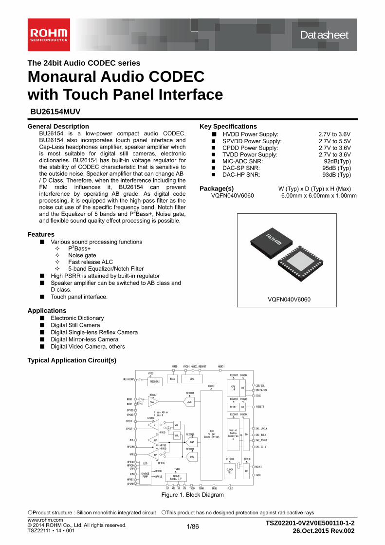
Typical Application Circuit(s)
Figure 1. Block Diagram
VQFN040V6060
ALCFilter
Sound Effect
SP
SPOUT+
SPOUT-
MICBIAS
CLOCKPLL
SerialAudio
InterFace
MCLKI
SAI_SDOUT
SAI_SDIN
SAI_BCLK
SAI_LRCLK
SDATA/SDA
SCLK
CSB/SCL
RESETB
CPUI/F
HVDD1 HGND2VMID
LDO
HPL
RESET
TSTO
REGOUT
REGOUT
HPVDD
SPVDD
REGOUT
HVDD
REGOUT
REGOUT
REGOUT
REGOUTREGOUT
ADC
REGOUT
HPR
HPVDD
MBIASCAP
MIN1
MIN2
HP
PGA
IO
IO
IO
IO
IOVDD
IOVDD
IOVDD
IOVDD
CPP
CPNHPVDD
HPVSS
HP
HPVSS
XP XN YP YN
TOUCHPANEL I/F
TVDD
TVDD
HPVSS
TGND
REGOUT
CPGND
Bias
Class AB orClass D
PLLC
DAC
DAC
IRQB
VOL
VOL
HPVSSCHARGEPUMP
CPVDD
HPVDDLDO
SPVDD
SPGND
HPCOM
HGND1

DatasheetDatasheet
2/86 TSZ02201-0V2V0E500110-1-2© 2014 ROHM Co., Ltd. All rights reserved.
26.Oct.2015 Rev.002
www.rohm.com
TSZ22111 • 15 • 001
BU26154MUV
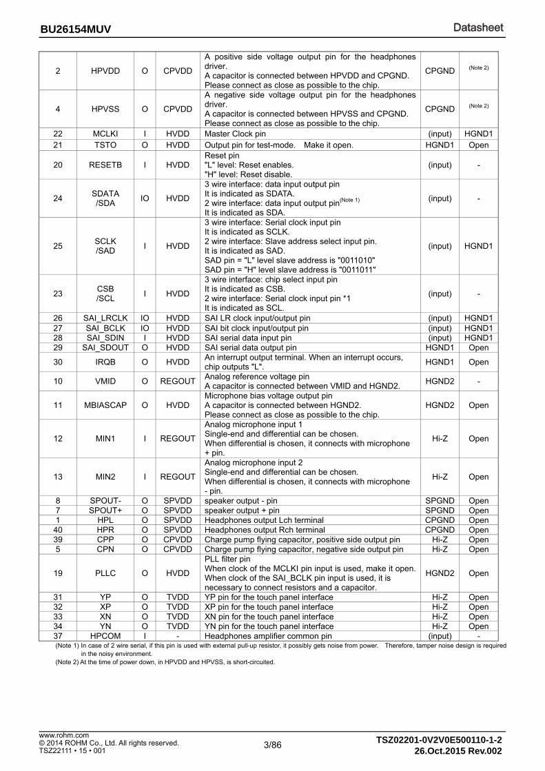
Pin Configuration(s)
Top view
Figure 2. Pin Configuration(s) Pin Description(s)
No Name I/O Power Function Reset
(Note1)No use(Note3)
17 HVDD P - High voltage power supply pin A capacitor is connected between HVDD and HGND1.
- -
6 SPVDD P - Speaker power supply pin A capacitor is connected between SPVDD and SPGND.
- -
38 CPVDD P - Voltage power supply pin for charge pump A capacitor is connected between CPVDD and CPGND.
- -
16 N.C - - A no connect pin. - -
36 TVDD P - Voltage power supply for the touch panel Please connect a capacitor between TVDD and TGND.
- -
15 HGND1 P - High voltage ground 1 It is used on the same voltage as HGND2, SPGND, CPGND, and TGND.
- -
14 HGND2 P - High voltage ground 2 It is used on the same voltage as HGND1, SPGND, CPGND, and TGND.
- -
9 SPGND P - Ground pin for Speaker It is used on the same voltage as HGND1, HGND2, CPGND, and TGND.
- -
3 CPGND P - Ground pin for charge pump It is used on the same voltage as HGND1, HGND2, SPGND, and TGND.
- -
35 TGND P - Ground pin for touch panel interface It is used on the same voltage as HGND1, HGND2, CPGND, and SPGND.
- -
18 REGOUT O HVDD Regulator output A capacitor is connected between REGOUT and HGND1. Please connect as close as possible to the chip.
HGND2 -
SD
AT
A/S
DA
SA
I_S
DO
UT
31
32
33
34
35
36
37
38
39
40
1 2 3 4 5 6 7 8 9 10
20
19
18
17
16
15
14
13
12
11
30 29 28 27 26 25 24 23 22 21
RESETB
SP
GN
D
SP
OU
T-
VM
ID
MBIASCAP
SP
VD
D
SP
OU
T+
XN
CPVDD
YN
CPP
TGND
HPR
TVDD
HPCOM
HP
L
HP
VS
S
REGOUT
SA
I_B
CL
K
SA
I_S
DIN
CS
B/S
CL
YP
IRQ
BXP
NC
SA
I_L
RC
LK
MC
LK
I
SC
LK
/SA
D
HVDD
HP
VD
D
HGND1
CP
GN
D
HGND2
TS
TO
MIN1
MIN2
CP
N
PLLC
DatasheetDatasheet
3/86 TSZ02201-0V2V0E500110-1-2© 2014 ROHM Co., Ltd. All rights reserved.
26.Oct.2015 Rev.002
www.rohm.com
TSZ22111 • 15 • 001
BU26154MUV
2 HPVDD O CPVDD
A positive side voltage output pin for the headphones driver. A capacitor is connected between HPVDD and CPGND. Please connect as close as possible to the chip.
CPGND (Note 2)
4 HPVSS O CPVDD
A negative side voltage output pin for the headphones driver. A capacitor is connected between HPVSS and CPGND. Please connect as close as possible to the chip.
CPGND (Note 2)
22 MCLKI I HVDD Master Clock pin (input) HGND121 TSTO O HVDD Output pin for test-mode. Make it open. HGND1 Open
20 RESETB I HVDD Reset pin "L" level: Reset enables. "H" level: Reset disable.
(input) -
24 SDATA /SDA
IO HVDD
3 wire interface: data input output pin It is indicated as SDATA. 2 wire interface: data input output pin(Note 1) It is indicated as SDA.
(input) -
25 SCLK /SAD
I HVDD
3 wire interface: Serial clock input pin It is indicated as SCLK. 2 wire interface: Slave address select input pin. It is indicated as SAD. SAD pin = "L" level slave address is "0011010" SAD pin = "H" level slave address is "0011011"
(input) HGND1
23 CSB /SCL
I HVDD
3 wire interface: chip select input pin It is indicated as CSB. 2 wire interface: Serial clock input pin *1 It is indicated as SCL.
(input) -
26 SAI_LRCLK IO HVDD SAI LR clock input/output pin (input) HGND127 SAI_BCLK IO HVDD SAI bit clock input/output pin (input) HGND128 SAI_SDIN I HVDD SAI serial data input pin (input) HGND129 SAI_SDOUT O HVDD SAI serial data output pin HGND1 Open
30 IRQB O HVDD An interrupt output terminal. When an interrupt occurs, chip outputs "L".
HGND1 Open
10 VMID O REGOUT Analog reference voltage pin A capacitor is connected between VMID and HGND2.
HGND2 -
11 MBIASCAP O HVDD Microphone bias voltage output pin A capacitor is connected between HGND2. Please connect as close as possible to the chip.
HGND2 Open
12 MIN1 I REGOUT
Analog microphone input 1 Single-end and differential can be chosen. When differential is chosen, it connects with microphone + pin.
Hi-Z Open
13 MIN2 I REGOUT
Analog microphone input 2 Single-end and differential can be chosen. When differential is chosen, it connects with microphone - pin.
Hi-Z Open
8 SPOUT- O SPVDD speaker output - pin SPGND Open 7 SPOUT+ O SPVDD speaker output + pin SPGND Open 1 HPL O SPVDD Headphones output Lch terminal CPGND Open
40 HPR O SPVDD Headphones output Rch terminal CPGND Open 39 CPP O CPVDD Charge pump flying capacitor, positive side output pin Hi-Z Open 5 CPN O CPVDD Charge pump flying capacitor, negative side output pin Hi-Z Open
19 PLLC O HVDD
PLL filter pin When clock of the MCLKI pin input is used, make it open. When clock of the SAI_BCLK pin input is used, it is necessary to connect resistors and a capacitor.
HGND2 Open
31 YP O TVDD YP pin for the touch panel interface Hi-Z Open 32 XP O TVDD XP pin for the touch panel interface Hi-Z Open 33 XN O TVDD XN pin for the touch panel interface Hi-Z Open 34 YN O TVDD YN pin for the touch panel interface Hi-Z Open 37 HPCOM I - Headphones amplifier common pin (input) - (Note 1) In case of 2 wire serial, if this pin is used with external pull-up resistor, it possibly gets noise from power. Therefore, tamper noise design is required
in the noisy environment. (Note 2) At the time of power down, in HPVDD and HPVSS, is short-circuited.

DatasheetDatasheet
4/86 TSZ02201-0V2V0E500110-1-2© 2014 ROHM Co., Ltd. All rights reserved.
26.Oct.2015 Rev.002
www.rohm.com
TSZ22111 • 15 • 001
BU26154MUV
Description of Block(s)
Figure 3. BU26154 Application circuit
SPOUT+
SPOUT- MCLKI
SAI_SDOUTSAI_SDIN
SAI_BCLK
SAI_LRCLK
SDATA/SDASCLK
CSB/SCL
RESETB
HVDD
HGND2
VMID
HPL
TSTO
HPR
MBIASCAP
CPP
CPN
XP
XN
YP
YN
TVDD
MIN1
HPVSS
TGND
REGOUT
CPGND
PLLC
IRQB
CPVDD
HPVDD
SPVDD
SPGND
CPUandDSP
TouchScreen
BU26154
MIN2
HPCOM HGND1
Open
1μF
2.2μF
2.2μF
1μF
2.2μF
2.2kohm 4.7μF
1μF 1μF 1μF 1μF
option
option
option
option
0.47μF
0.47μF
DatasheetDatasheet
5/86 TSZ02201-0V2V0E500110-1-2© 2014 ROHM Co., Ltd. All rights reserved.
26.Oct.2015 Rev.002
www.rohm.com
TSZ22111 • 15 • 001
BU26154MUV
Absolute Maximum Ratings (Ta = 25°C) (HGND1=HGND2=SPGND=CPGND=TGND=0V)
Parameter Symbol Condition Rating Unit
HVDD Supply Voltage HVDD - -0.3 to 4.5 V
SPVDD Supply Voltage SPVDD - -0.3 to 7.0 V
CPVDD Supply Voltage CPVDD - -0.3 to 4.5 V
Input Voltage VIN
MCLKI, SAI_LRCLK, SAI_BCLK, SAI_SDIN,
SDATA/SDA, SCLK. CSB/SCL pins
-0.3 to HVDD+0.3 V
MIN1, MIN2 pins -0.3 to REGOUT+0.3 V
Storage Temperature Tstg - -55 to +150
Power Dissipation(Note 1) Pd
Ta=25°C (Note 1) 0.80 W
Ta=25°C (Note 2) 3.01 W
Output Current 1 IOSP SPOUT+, SPOUT- pins -560 to +560 mA
Output Current 2 IOHP HPL, HPR pins -100 to +100 mA
Output Current 3 IOCP HPVSS,HPVDD,CP,CN
pin -500 to +500 mA
Output Current 4 IOREGO REGOUT pin -30 to 0 mA
Output Current 5 IOO
Except SPOUT+,SPOUT-,HPL,HPR,
REGOUT,HPVDD,HPVSS pins
-8 to +8 mA
Do not short the output pin to another output pin, power supply pin or GND pin.(Output pin includes an IO pin which is in output mode) (Note 1) 74.2mm×74.2mm×1.6tmm FR4 1Layer Glass epoxy base Surface Copper foil 0%)Mounting
Above Ta=25,reduced by 8.0mW/. Thermal beer is on a base. (Note 2) 74.2mm×74.2mm×1.6tmm FR4. 4 Layer Glass epoxy base(2,3layer Copper foil 100%)Mounting
Above Ta=25, reduced by 30.12mW/. Thermal beer is on a base. Caution: Operating the IC over the absolute maximum ratings may damage the IC. The damage can either be a short circuit between pins or an open circuit between pins and the internal circuitry. Therefore, it is important to consider circuit protection measures, such as adding a fuse, in case the IC is operated over the absolute maximum ratings.
Recommended Operating Conditions
(HGND1=HGND2=SPGND=CPGND=TGND=0V)
Parameter Symbol Condition Rating Unit
HVDD Supply Voltage HVDD HVDD=CPVDD=TVDD 2.7 to 3.6 V
SPVDD Supply Voltage SPVDD - 2.7 to 5.5 V
CPVDD Supply Voltage CPVDD HVDD=CPVDD=TVDD 2.7 to 3.6 V
TVDD Supply Voltage TVDD HVDD=CPVDD=TVDD 2.7 to 3.6 V
Operating Temperature Top - -20 to +85
(Note 1) The radiation-proof design is not carried out.

DatasheetDatasheet
6/86 TSZ02201-0V2V0E500110-1-2© 2014 ROHM Co., Ltd. All rights reserved.
26.Oct.2015 Rev.002
www.rohm.com
TSZ22111 • 15 • 001
BU26154MUV
Electrical Characteristics DC Characteristics (HGND1= HGND2=SPGND=CPGND=TGND=0V, HVDD=3.3V, SPVDD=3.3V, CPVDD=3.3V, TVDD=3.3V, Ta=25)
Parameter Symbol Conditions Min Typ Max Unit Related Pin
"H" Input Voltage1 VIH1 HGND1=0V HVDD *0.8 - HVDD+0.3 V All Digital
Input
"L" Input Voltage 1 VIL1 HGND1=0V -0.3 - HVDD *0.2 V All Digital
Input
"H" Input Voltage 2 VIH2 HGND1=0V HVDD-0.4 - HVDD+0.3 V All Digital
Input
"L" Input Voltage 2 VIL2 HGND1=0V -0.3 - 0.4 V All Digital
Input "H" output Voltage VOH IOH=-1mA HVDD *0.85 - - V Except SDA "L" output Voltage 1 VOL1 IOL=1mA - - HVDD *0.15 V Except SDA "L" output Voltage 2 VOL2 IOL=3mA - - 0.4 V SDA "H" Input Leakage Current
IIH VIH= HVDD - - 10 µ A All Digital
Input "L" Input Leakage Current
IIL VIL=HGND1 -10 - - µ A All Digital
Input "Z" output Leakage Current
IOZH VOH=HVDD - - 10 µ A SDA
"Z" output Leakage Current
IOZL VOL=HGND1 -10 - - µ A SDA
Operating Current1 IDDO1
Playback(fs48kHz) no Load, Hp-amp
use Sin1kHz-Full Scale
output
- 10 13 mA -
Operating Current2 IDDO2
Playback(fs48kHz) no Load, D-class,
Sp-amp use Sin1kHz-Full Scale
output
- 10.5 13.7 mA -
Operating Current3 IDDO3
Playback(fs48kHz) no Load, AB-class,
Sp-amp use Sin1kHz-Full Scale
output
- 12 15.6 mA -
Operating Current4 IDDO4 Record(fs48kHz)
Sin1kHz-Full Scale input
- 9.5 12.4 mA -
Operating Current5 IDDO5 Touch Panel
Interface Operate - 0.6 1 mA -
Operating Current6 (Note 3)
IDDO6
Touch Panel Interface Interrupt
Wait Ta = -40 to 55
- 220 320 uA -
Standby Current IDDS 25 - 0.5 5 µ A - (Note 1) Touch Panel Interface Interrupt electric current at the time of the wait. Please refer to a touch panel interface clause for the movement setting
condition. (Note 2) Standby current is total value for all power supply currents. (Note 3) Standby current's condition is power off state by RESETB=L

DatasheetDatasheet
7/86 TSZ02201-0V2V0E500110-1-2© 2014 ROHM Co., Ltd. All rights reserved.
26.Oct.2015 Rev.002
www.rohm.com
TSZ22111 • 15 • 001
BU26154MUV
AC Characteristics
Clock PLL not used (HGND1= HGND2=SPGND=CPGND=TGND=0V, HVDD=3.3V, SPVDD=3.3V, CPVDD=3.3V, TVDD=3.3V, Ta=25)
Parameter Symbol Min Max Unit
MCLKI Frequency fC 4.096 49.152 MHz
MCLKI Period tC 1/fC 1/fC ns
MCLKI “H” Length tCH tC*0.4 - ns
MCLKI “L” Length tCL tC*0.4 - ns
PLL used (HGND1= HGND2=SPGND=CPGND=TGND=0V, HVDD=3.3V, SPVDD=3.3V, CPVDD=3.3V, TVDD=3.3V,Ta=25)
Parameter Symbol Min Max Unit
MCLKI Frequency fC 6.75 54 MHz
MCLKI Period tC 1/fC 1/fC ns
MCLKI “H” Length tCH tC*0.4 - ns
MCLKI “L” Length tCL tC*0.4 - ns
When PLL is use, clock from SAI_BCLK pin other than MCLKI pin could be inputted. Please refer to SAI slave clause about the BCLK pin input frequency.
Figure 4
Reset (HGND1= HGND2=SPGND=CPGND=TGND=0V, HVDD=3.3V, SPVDD=3.3V, CPVDD=3.3V, TVDD=3.3V, Ta=25)
Parameter Symbol Min Max. Unit
RESETB pulse width tW_RST 5 - µ s
Figure 5
When Reset pin is made low-level, internal LDO goes to power mode. 1ms is necessary until REGOUT pin becomes low-level. The recommended tW_RST is over 1ms.
MCLKI
tC, fC
tCH tCL
RESETB
tW_RST

DatasheetDatasheet
8/86 TSZ02201-0V2V0E500110-1-2© 2014 ROHM Co., Ltd. All rights reserved.
26.Oct.2015 Rev.002
www.rohm.com
TSZ22111 • 15 • 001
BU26154MUV
2-Wire Serial Interface (HGND1= HGND2=SPGND=CPGND=TGND=0V, HVDD=3.3V, SPVDD=3.3V, CPVDD=3.3V, TVDD=3.3V, Ta=25, CL=30pF)
Parameter Symbol Standard Mode Fast Mode
Unit Min Max Min Max
SCL Frequency fSCL - 100 - 400 kHz
SCL "L" Length tLOW 4.7 - 1.3 - µs
SCL "H" Length tHIGH 4.0 - 0.6 - µs
Hold Time under Repeat [Start] Condition tHD:STA 4.0 - 0.6 - µs
Setup Time under Repeat [Start] Condition tSU:STA 4.0 - 0.6 - µs
Data Hold Time tHD:DAT 0 3.45 0 0.9 µs
Data Setup Time tSU:DAT 250 - 100 - ns
Setup Time under [Stop] Condition tSU:STO 4.0 - 0.6 - µs
Figure 6
SDA
tHD:STA tHD:DAT
tLOW
tHIGH
tSU:DAT
tSU:STO tSU:STA
SCL
tHD:STA

DatasheetDatasheet
9/86 TSZ02201-0V2V0E500110-1-2© 2014 ROHM Co., Ltd. All rights reserved.
26.Oct.2015 Rev.002
www.rohm.com
TSZ22111 • 15 • 001
BU26154MUV
3-Wire Serial Interface (HGND1= HGND2=SPGND=CPGND=TGND=0V, HVDD=3.3V, SPVDD=3.3V, CPVDD=3.3V, TVDD=3.3V, Ta=25, CL=30pF)
Parameter Symbol Min Max Unit
SCLK Low to Chip Select enable tSLCL 100 - ns
Chip Select Enable to SCLK Low tCLSL 100 - ns
Chip Select Enable to SCLK High tCLSH 100 - ns
CLK High to Chip Select enable tSHCL 100 - ns
SCLK High Pulse Width tSH 50 - ns
SCLK Low Pulse Width tSL 50 - ns
Input Data Setup time tIDS 30 - ns
Input Data Hold time tIDH 30 - ns
SCLK last edge to Chip Select disable tCHS2 100 - ns
Chip Select High Pulse Width tCH 100 - ns
Output Data Valid tODV - 40 ns
Chip Select High to Data Transition tCHDTS - 40 ns
Two kinds of timing are supported depending on the SCLK pin level at data transfer start. Read or Write is selected by LSB logic INDEX.
Figure 7

DatasheetDatasheet
10/86 TSZ02201-0V2V0E500110-1-2© 2014 ROHM Co., Ltd. All rights reserved.
26.Oct.2015 Rev.002
www.rohm.com
TSZ22111 • 15 • 001
BU26154MUV
Serial Audio Interface (Slave) (HGND1= HGND2=SPGND=CPGND=TGND=0V, HVDD=3.3V, SPVDD=3.3V, CPVDD=3.3V, VDD=3.3V, Ta=25, CL=30pF)
Parameter Symbol Min Max Unit
SAI_BCLK Period tC_BCLK 32fs 128fs Hz
SAI_BCLK "H" Length tHW_BCLK 73 - ns
SAI_BCLK "L" Length tLW_BCLK 73 - ns
SAI_LRCLK Hold Time tH_LRCLK 20 - ns
SAI_LRCLK Setup Time tSU_LRCLK 20 - ns
SAI_SDOUT Delay Time tD_SDO (Note 1) - 80 ns
SAI_SDIN Setup Time tSU_SDI 20 - ns
SAI_SDIN Hold Time tH_SDI 20 - ns
(Note 1) tD_SDO is the delay time from previous SAI_BCLK transition and SAI_LRCLK transition.
SAI Transmit
Figure 8
SAI Receive
Figure 9
SAI_LRCLK
SAI_BCLK
SAI_SDOUT
tC_BCLK tSU_LRCLK tH_LRCLK
tD_SDO
tHW_BCLK tLW_BCLK
SAI_LRCLK
SAI_BCLK
SAI_SDIN
tC_BCLK tSU_LRCLK tH_LRCLK
tSU_SDI tH_SDI
tHW_BCLK tLW_BCLK

DatasheetDatasheet
11/86 TSZ02201-0V2V0E500110-1-2© 2014 ROHM Co., Ltd. All rights reserved.
26.Oct.2015 Rev.002
www.rohm.com
TSZ22111 • 15 • 001
BU26154MUV
SAI (Master) - Serial Audio Interface (Master) (HGND1= HGND2=SPGND=CPGND=TGND=0V, HVDD=3.3V, SPVDD=3.3V, CPVDD=3.3V, TVDD=3.3V, Ta=25, CL=30pF)
Parameter Symbol Min Max Unit
SAI_BCLK Period tC_BCLK 32fs 64fs Hz
SAI_BCLK "H" Length tHW_BCLK 146 - ns
SAI_BCLK "L" Length tLW_BCLK 146 - ns
SAI_LRCLK Delay time tD_LRCLK - 20 ns
SAI_SDOUT Delay Time tD_SDO - 20 ns
SAI_SDIN Setup Time tSU_SDI 50 - ns
SAI_SDIN Hold Time tH_SDI 0 - ns
SAI Transmit
Figure 10
SAI Receive Figure 11
SAI_BCLK
SAI_SDOUT
tC_BCLK tD_LRCLK
tD_SDO
tHW_BCLK tLW_BCLK
SAI_LRCLK
SAI_LRCLK
SAI_BCLK
SAI_SDIN
tC_BCLK tD_LRCLK
tSU_SDI tH_SDI
tHW_BCLK tLW_BCLK

DatasheetDatasheet
12/86 TSZ02201-0V2V0E500110-1-2© 2014 ROHM Co., Ltd. All rights reserved.
26.Oct.2015 Rev.002
www.rohm.com
TSZ22111 • 15 • 001
BU26154MUV
Power Supply Sequence
Please power on/off the LSI with all kind of power at the same time. Each power supply should power up/down in 50ms. Also, keep all power supply in the ON state or the OFF state. Please avoid partial ON or partial OFF states. Please keep RESETB pin “L” level until all power supply become ON state. The CPU I/F become available when all power supply is powered on after tW_PURST and tW_REGU time exceeds. HVDD must be powered on first, but HVDD must be powered off last. About SPVDD, there is no limitation above.
Parameter Symbol Min Typ Max Unit
Power On Delay Time tVDD_ON 0 - 50 ms
Power Off Delay Time tVDD_OFF 0 - 50 ms
Reset Time after Power ON tw_PURST 1 - - μs
Wait Time for Regulator Starting after Reset Release
tw_REGU 1 - - ms
Figure 12
H VDD Power supply t VDD_ON
PowerSupply*0.9
PowerSupply*0.9 tVDD_OFF
not available available not available CPU I/F
RESETB
Other
Power
supply
VDD OFF Operation VDD OFF STATUS
PowerDown Wait Regulator
t W_REGU PowerSupply*0.1
PowerSupply*0.1
REGOUT
tW_ PURST

DatasheetDatasheet
13/86 TSZ02201-0V2V0E500110-1-2© 2014 ROHM Co., Ltd. All rights reserved.
26.Oct.2015 Rev.002
www.rohm.com
TSZ22111 • 15 • 001
BU26154MUV
Analog Characteristics (HGND1= HGND2=SPGND=CPGND=TGND=0V, HVDD=3.3V, SPVDD=3.3V, CPVDD=3.3V, TVDD=3.3V, Ta=25°C)
Parameter Symbol Condition Min Typ Max Unit
Regulator Output
REGOUT Output Level VREGOUT - 1.7 1.8 1.9 V
Mic Input (MIC Gain=18dB / Digital Volume=0.0dB / ALC=OFF)
Full Scale Input Signal Level VMINFS1 MIN1,MIN2 - -
0.124 Vp-p
Input Resistance RMIN1 MIN1,MIN2 20 30 40 kΩ
Mic Input (MIC Gain=9.0dB / Digital Volume=0.0dB / ALC=OFF)
Full Scale Input Signal Level VMINFS2 MIN1,MIN2 - - 0.454 Vp-p
Input Resistance RMIN2 MIN1,MIN2 20 30 40 kΩ
Analog Reference Level(VMID-pin)
Analog Reference Voltage VREF - 0.9x
REGOUT/21.0x
REGOUT/2 1.1x
REGOUT/2 V
Microphone Bias(MBIASCAP -pin)
Output Voltage where, VMIC<HVDD*0.85 VMIC
IMIC = -1mA, MICBCON=0
1.50x REGOUT/2
1.67x REGOUT/2
1.84x REGOUT/2
V
IMIC = -1mA, MICBCON=1
2.00x REGOUT/2
2.22x REGOUT/2
2.45x REGOUT/2
V
IMIC = -1mA, MICBCON=2
2.50x REGOUT/2
2.78x REGOUT/2
3.06x REGOUT/2
V
IMIC = -1mA, MICBCON=3
3.00x REGOUT/2
3.33x REGOUT/2
3.67x REGOUT/2
V
Output Current IMIC - - - 2 mA

DatasheetDatasheet
14/86 TSZ02201-0V2V0E500110-1-2© 2014 ROHM Co., Ltd. All rights reserved.
26.Oct.2015 Rev.002
www.rohm.com
TSZ22111 • 15 • 001
BU26154MUV
(HGND1=HGND2=SPGND=CPGND=TGND=0V, HVDD=3.3V, SPVDD=3.3V, CPVDD=3.3V, TVDD=3.3V, Ta=25) Parameter Symbol Conditions Min Typ Max Unit
Analog Inputs to ADC out (MIC Gain=18dB / Digital Volume=0.0dB / ALC=OFF)
S/(N+D) SND1 -1dBFS/ A-weighted - 78 - dB
S/N SNR1 A-weighted - 89 - dB
Power Supply Rejection Ratio PSRR1 HVDD on 100mVp-p, 1kHznoise, no signal input
- 90 - dB
Analog Inputs to ADC out (MIC Gain=9.0dB / Digital Volume=0.0dB / ALC=OFF)
S/(N+D) SND2 -1dBFS/ A-weighted - 80 - dB
S/N SNR2 A-weighted - 92 - dB
Power Supply Rejection Ratio PSRR2 HVDD on 100mVp-p, 1kHz noise, no signal input - 90 - dB
DAC to Headphone OUT(HPR/HPL, with 16Ω/50pF load)
Total Harmonic Distortion THD+N3 1kHz,input -12dBFS - 75 - dB
Signal to Noise Ratio SNR3 A-weighted - 93 - dB
Power Supply Rejection Ratio PSRR3
HVDD on100mVp-p,1kHz noise, no
signal input - 90 - dB
CPVDD on100mVp-p,1kHz noise, no
signal input - 90 - dB
Output Offset Voltage VOF No signal input - ±1 - mV
Charge Pump Oscillator Frequency CPOSC - - 500 - kHz
HPVDD Port Output Voltage HPVDO - - 1.8 - V
HPVSS Port Output Voltage HPVSO - - -1.8 - V
DAC to Speaker OUT D-class Mode (SPOUT+/-, with 8Ω/50pF load)
Output Power Po4 THD=10%, SPVOL=6dB - 700 - mW
Total Harmonic Distortion THD+N4 Po=310mW - 66 - dB
Signal to Noise Ratio SNR4 A-weighted, THD+N=1% - 95 - dB
Power Supply Rejection Ratio PSRR4
HVDD on100mVp-p,1kHz noise
- 90 - dB
SPVDD on100mVp-p,1kHz noise - 60 - dB
PWM frequency PWMF - - 370 - kHz
Efficiency EFF - - 90 - %
DAC to Speaker OUT AB-class Mode (SPOUT+/-, with 8Ω/50pF load)
Output Power Po5 THD=10%, SPVOL=6dB - 700 - mW
Total Harmonic Distortion THD+N5 Po=310mW - 62 - dB
Signal to Noise Ratio SNR5 A-weighted, THD+N=1% - 95 - dB
Power Supply Rejection Ratio PSRR5
HVDD on100mVp-p,1kHz noise
- 90 - dB
SPVDD on100mVp-p,1kHz noise - 60 - dB
Microphone Bias(MBIASCAP-pin) *1
Output Noise Voltage VMICN622Hz to 22kHz,MICBCON=1 - 5 - μV
Power Supply Rejection Ratio PSRR6
HVDD on100mVp-p,1kHz noise
Load=1mA MICBCON=1
- 70 - dB

DatasheetDatasheet
15/86 TSZ02201-0V2V0E500110-1-2© 2014 ROHM Co., Ltd. All rights reserved.
26.Oct.2015 Rev.002
www.rohm.com
TSZ22111 • 15 • 001
BU26154MUV
(HGND1=HGND2=SPGND=CPGND=TGND=0V, HVDD=3.3V, SPVDD=3.3V, CPVDD=3.3V, TVDD=3.3V,Ta=25) Parameter Symbol Conditions Min Typ Max Unit
Touch Panel Interface
ADC Resolution N - - - 12 Bit
Differential Non-Linearity Error DNL - -3 - 3 LSB
Integral Non-Linearity Error INL - -4 - 4 LSB
Offset Error OFTERR - - 1 - LSB
Gain Error GAERR - - 0.5 - LSB
Touch Panel Driver Switch SWONR - - 5 - Ω
Interrupt Pull-up Resistance IRQR1 RSEL=0 40 50 70 kΩ
IRQR2 RSEL=1 70 90 120 kΩ
ADC Conversion Timing Tw_ADC1 - - 35 μs
Tw_ADC2 - - 43 μs

DatasheetDatasheet
16/86 TSZ02201-0V2V0E500110-1-2© 2014 ROHM Co., Ltd. All rights reserved.
26.Oct.2015 Rev.002
www.rohm.com
TSZ22111 • 15 • 001
BU26154MUV
Function Description Clock Control Main modules that make sound path of the LSI inside operate with 1024fs Audio Clock. Audio Clock can be selected whether divided clock of 256fs/512fs/1024fs from MCLKI or generated clock from Audio PLL. When PLL is used, PLL generates internal clock. The input clock into PLL can be selected from either MCLKI port or SAI_BCLK port by setting Clock Input / Output Control register. PLL generates 256fs clock of sampling frequency. The registers about Audio Clock setting: Sampling Rate Setting Register, FPLLM, FPLLNL, FPLLNH, FPLLD, FPLLFL, FPLLFH, FPLLFDL, FPLLFDH, Clock Input / Output Control register, Clock Input Select Register ・The sequence of PLL setting 1. Stop PLL output by setting PLLOE bit to “0”. 2. Disable PLL by setting PLLEN bit to “0”. 3. Set PFLLM, FPPNL, FPLLNH, FPLLD, FPLLFL, FPLLFH, FPLLFDL, FPLLFDH. 4. Set input port by PLLISEL bit. 5. Set PLLEN bit to “1”. 6. Wait for the PLL stabilizing time as the table “PLL Stabilizing Time”. 7. Set PLLOE bit to “1”. 8. Start recording or playback.
PLL Stabilizing Time PLL stability time
10msec - Related Register Sampling Rate Setting Register PLLNL, PLLNH Register PLLML, PLLMH Register PLLDIV Register Clock Enable Register Clock Input / Output Control Register

DatasheetDatasheet
17/86 TSZ02201-0V2V0E500110-1-2© 2014 ROHM Co., Ltd. All rights reserved.
26.Oct.2015 Rev.002
www.rohm.com
TSZ22111 • 15 • 001
BU26154MUV
When PLL is Used. The LSI support audio PLL function that can generate precise audio clock from wide range of clock frequency. Then, it can be realize audio function without external clock generator for audio. The LSI supports following cases. The LSI generates audio clock with input clock provided from MCLKI port or BCLKI port. case1: PLLISEL (0x0e/0x0f)=0x1, MST(0x64/0x65)="0" Audio clock is generated by the PLL BU26154 with MCLKI clock. SAI_LRCLK and SAI_BCLK are provided by the CPU.
SAI_LRCLKSAI_BCLKSAI_SDINSAI_SDOUT
B26154
CPU
MCLKICLOCK
Figure 13
case2: PLLISEL (0x0e/0x0f)=0x1, MST(0x64/0x65)="1" Audio clock is generated by the PLL in BU26154 from MCLKI clock. SAI_LRCLK and SAI_BCLK are provided from the LSI.
Figure 14
case3: PLLISEL (0x0e/0x0f)=0x2, MST(0x64/0x65)="1" Audio clock is generated by PLL in BU26154 form SAI clock.
Figure 15

DatasheetDatasheet
18/86 TSZ02201-0V2V0E500110-1-2© 2014 ROHM Co., Ltd. All rights reserved.
26.Oct.2015 Rev.002
www.rohm.com
TSZ22111 • 15 • 001
BU26154MUV
When PLL is not Used. Audio clock is generated by the CPU and supplied to the LSI when PLL is not used. Then CPU and the LSI are synchronized. case 5: MST (0x64/0x65) ="0" Audio clock (256fs, 512fs, 1024fs) is generated by the CPU and supplied to MCLKI port of the LSI. LRCLK and BCLK are also provided from the CPU.
Figure 16
case6: MST (0x64/0x65)="1" Audio clock (256fs, 512fs, 1024fs) is generated by the CPU and supplied to MCLKI port of the LSI. SAI_LRCLK and SAI_BCLK are provided from the LSI.
Figure 17
Even when using the same sampling frequency, the setting condition is different depending on clock frequency. When changing MCLKI input frequency, PLLOE should be set to “0”, then PLLOE should be set to “1” back.
DatasheetDatasheet
19/86 TSZ02201-0V2V0E500110-1-2© 2014 ROHM Co., Ltd. All rights reserved.
26.Oct.2015 Rev.002
www.rohm.com
TSZ22111 • 15 • 001
BU26154MUV
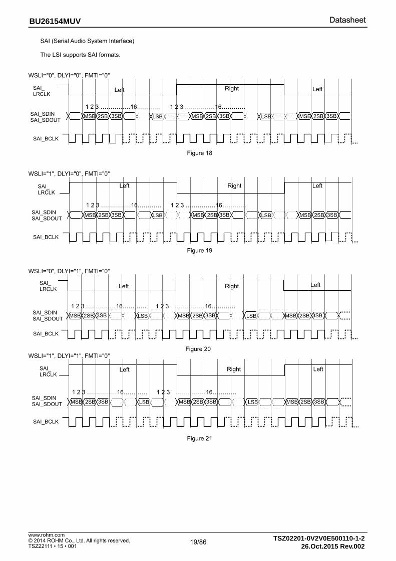
SAI (Serial Audio System Interface) The LSI supports SAI formats.
WSLI="0", DLYI="0", FMTI="0"
Figure 18 WSLI="1", DLYI="0", FMTI="0"
Figure 19 WSLI="0", DLYI="1", FMTI="0"
Figure 20
WSLI="1", DLYI="1", FMTI="0"
Figure 21
Left
MSB 2SB 3SB LSB
Right
1 2 3 ……………16………… 1 2 3 ……………16…………
Left
MSB 2SB 3SB LSB MSB 2SB 3SB
SAI_ LRCLK
SAI_SDIN SAI_SDOUT
SAI_BCLK
Right
1 2 3 ……………16………… 1 2 3 ……………16…………
Left Left
MSB 2SB 3SB LSB MSB 2SB 3SB LSB MSB 2SB 3SB
SAI_ LRCLK
SAI_SDIN SAI_SDOUT
SAI_BCLK
1 2 3 ……………16………… 1 2 3 ……………16…………
Left Left Right SAI_ LRCLK
SAI_SDIN SAI_SDOUT
SAI_BCLK
MSB 2SB 3SB LSB MSB 2SB 3SB LSB MSB 2SB 3SB
1 2 3 ……………16………… 1 2 3 ……………16…………
Left Right Left
MSB 2SB 3SB LSB MSB 2SB 3SB LSB MSB 2SB 3SB
SAI_ LRCLK
SAI_SDIN SAI_SDOUT
SAI_BCLK

DatasheetDatasheet
20/86 TSZ02201-0V2V0E500110-1-2© 2014 ROHM Co., Ltd. All rights reserved.
26.Oct.2015 Rev.002
www.rohm.com
TSZ22111 • 15 • 001
BU26154MUV
DLYI="0", FMTI="1" Flame synchronous transfer mode: R channel data is transferred right after L channel data.
Figure 22
DLYI="1", FMTI="1" Flame synchronous transfer mode: R channel data is transferred right after L channel data.
Figure 23
- Related Register SAI Transmitter Control Register SAI Receiver Control Register
Right
1 2 3 ……………16 1 2 3 ……………16…………
Left Left
MSB 2SB 3SB LSBMSB 2SB 3SB LSB MSB 2SB 3SB
SAI_ LRCLK
SAI_SDIN SAI_SDOUT
SAI_BCLK
1 2 3 ……………16 1 2 3 …………16…………
Left Right Left SAI_ LRCLK
SAI_SDIN SAI_SDOUT
SAI_BCLK
MSB 2SB 3SB LSBMSB 2SB 3SB LSB MSB 2SB 3SB

DatasheetDatasheet
21/86 TSZ02201-0V2V0E500110-1-2© 2014 ROHM Co., Ltd. All rights reserved.
26.Oct.2015 Rev.002
www.rohm.com
TSZ22111 • 15 • 001
BU26154MUV
2 wire serial interface
This LSI has 2 wire serial interfaces. The LSI operates as a slave device. The address is fixed at “0011010”. - Format The followings are the protocol of the LSI. Write (MSB first) Start Condition (Set SDA level from “H” to “L” during SCL=“H”) Slave Address (0011010) +W (0) (8bit) Write Address (8bit) Write Data (8bit) … Stop Condition (Set SDA level from “L” to “H” during SCL=“H”) Read (MSB first) Start Condition Slave Address (0011010) +W (0) (8bit) Read Address (8bit) (Stop Condition) Start Condition Slave Address (0011010) +R (1) (8bit) Read Data (8bit) The following shows the wave form of the LSI. The yellow gridding shows that slave device drives the bus. The symbol in the wave form means as following table.
Unit Description
W/R 0: It is Read Write 1
A 0: ACK(Acknowledge) 1: NAK(Not Acknowledge)
A[7-0] Address (8bit)
D[7-0] Data(8bit)
Write
A
SCL Start
SDA
1 2 3 4 5 6 7 8 0 1 2 3 4 5 6 7 80 1 2 3 4 5 6 7 80
Continued from the above
1 2 3 4 5 6 7 8 0 1 2 3 4 5 6 7 808 1 2 3 4 5 6 7 Stop0
slave address reception Access address reception Write data reception
Write data reception Write data reception Write data reception
0 W A7 A6 A5 A4 A3 A2 A1 A0A D7 D6 D5 D4 D3 D2 D1 D00 1 1 0 0 1 A
A A AA
Internal write
D7 D6 D5 D4 D3 D2 D1 D0D7 D6 D5 D4 D3 D2 D1 D0 D7 D6 D5 D4 D3 D2 D1 D0
Internal writeInternal write
Figure 24
In case there is no Stop or Start condition after internal register is written (Above figure: Internal Write), the slave device becomes continuous write mode and the next received 8 bits of data will be written into the internal register addressed by incremented by two to the current address.

DatasheetDatasheet
22/86 TSZ02201-0V2V0E500110-1-2© 2014 ROHM Co., Ltd. All rights reserved.
26.Oct.2015 Rev.002
www.rohm.com
TSZ22111 • 15 • 001
BU26154MUV
Read
Start
SCL
SDA
1 2 3 4 5 6 7 8 0 1 2 3 4 5 6 7 80
1 2 3 4 5 6 7 8 0 1 2 3 4 5 6 7 80Start
A
Internal read
1 2 3 4 5 6 7 80
slave address reception Access address reception
slave address reception Read data transmission Read data transmission
S
R
0 W A7 A6 A5 A4 A3 A2 A1 A0 A
A A
0 1 1 0
0 0 1 1
Continued from the above
0 1
0 1 0 A D7 D6 D5 D4 D3 D2 D1 D0D7 D6 D5 D4 D3 D2 D1 D0
Internal read
Figure 25
If the Master device returns ACK (acknowledge) after the 8 bit data transferred from the LSI becomes continuous read mode. The next received 8 bits of data will be read from the internal register addressed by incremented by two to the current address.

DatasheetDatasheet
23/86 TSZ02201-0V2V0E500110-1-2© 2014 ROHM Co., Ltd. All rights reserved.
26.Oct.2015 Rev.002
www.rohm.com
TSZ22111 • 15 • 001
BU26154MUV
State transition about sound control The following shows state transition about sound control. A change state is carried out by RECPLAY bit setup.
Figure 26
(1) Sound Stop STATE (RECPLAY=0x0)
Sound activity is stopped. (2) Rec STATE (RECPLAY =0x1)
Recording is enabled through microphone. (3) Play STATE (RECPLAY =0x2)
Playback is enabled from SAI. (4) Monitor STATE (RECPLAY =0x7)
Monitoring recording via microphone is enabled. ALC function is only effective in recording path. Only 2ch sound effects are available in Notch filter mode. In the time of transition Rec STATE to Monitor STATE, please set off the register bits of EQ2EN-EQ3EN.
(5) Rec and Play STATE (RECPLAY =0x3) Playback is enabled from SAI with recording via microphone. ALC function is only effective in recording path. Only 2ch sound effects are available in Notch filter mode. In the time of transition Rec STATE to Monitor STATE, please set off the register bits of EQ2EN-EQ3EN.
Sound Stop STATE
0x0
Rec STATE0x1
Play STATE0x2
Rec and PlaySTATE
0x3
Monitor STATE0x7
BU26154MUV is changed
status by setting RECPLAY
bit.

DatasheetDatasheet
24/86 TSZ02201-0V2V0E500110-1-2© 2014 ROHM Co., Ltd. All rights reserved.
26.Oct.2015 Rev.002
www.rohm.com
TSZ22111 • 15 • 001
BU26154MUV
Signal Flow It uses signal flow Case1 or Case2 at the time of recording (analog microphone). Case1:
RECDATT
FilterADCDigital
Interface
DVMUTE
ALC
AMICVOL
RECALCVOL
Recording
NoiseGate
RECLPF
HPF2HPF1
Filter Block
Case2:
RECDATT
FilterADCDigital
Interface
DVMUTE
ALC
AMICVOL
RECALCVOL
Recording
NoiseGate
RECLPF
HPF2HPF1
Filter Block
Figure 27
Name Function Related Register Setting
AMICVOL Analog Microphone volume Mic input volume control Volume setting 9dB to +35.25dB
HPF1 High path filter for record DC cut DSP Filter Function Enable HPF Enable/Disable
HPF2 High pass Filter for Record DSP Filter Function Enable
HPF Enable/Disable order setting
High Pass Filter2 Cut-off Control Cut-off frequency setting
Filter Notch filter is available
Sound Effect Mode Sound Effect mode setting DSP Filter Function Enable Each filters Enable/Disable settingEQ Band N Gain Setting Each filters gain setting Programmable EQ Band N Coeffeicient-a0/1
Each sound effects characteristics setting
RECLPF Low pass Filter for recording. Rec Programmable LPF Setting
LPF Enable/Disable setting order setting
Rec Programmable LPF Cutoff Coef
Cut-off frequency setting
REC ALCVOL
ALC use:ALC controls volume ALC not use: It’s available as Boost volume
refer to application note ALC
Auto Level Controller Function. ALC is processed to recording data
Noise Gate The purpose is for reducing a floor noise
RECDATT
Record Digital Attenuator. It’s available fader function for reducing a Pop-noise when changing volume.
Record Digital Attenuator Control Record Digital Attenuator Control Digital Volume Control Function Enable
Digital Volume Control Function Enable
Mixer & Volume Control Mixer & Volume Control
DVMUTE Record Digital Volume Mute Digital Volume Control Function Enable
Digital Volume Control Function Enable
* Please refer to the Sound Effect Mode register for Filter Block. When Filter Block is connected with the reproduction route, nothing is processed in the recording route.

DatasheetDatasheet
25/86 TSZ02201-0V2V0E500110-1-2© 2014 ROHM Co., Ltd. All rights reserved.
26.Oct.2015 Rev.002
www.rohm.com
TSZ22111 • 15 • 001
BU26154MUV
Signal flow at the time of the reproduction
LRMCON
PLAYALCVOL
PLAYDATT
FilterEffect
VolDigital
InterfaceDAC
ALCDV
MUTE
Playback
SPVOLPLAYLPF
Filter Block
SOFTCLIPAVOLAVOLVOL
To Speaker ampifier
To Headphone ampifier
HPF2 H-BASS
HPINSEL
AVOLSPINSEL
Figure 28
Name Function Related Register Setting
LRMCON Mixer of the Lch/Rch data input from SAI.
Mixer & Volume Control Mixer setting
Effect Vol It is digital before the sound is processed Volume.
Playback Effect Volume Volume setting -71.5dB to 0dB (0.5dBstep)
P2Bass+ Block for P2Bass + processing. P2Bass+ Enable P2Bass+ Parameter*
Setting of P2Bass+
Filter Notch filter is available
Sound Effect Mode Sound mode setting DSP Filter Function Enable Enable/Disable of each filter EQ Band N Gain Setting Gain setting of each filter Programmable EQ Band N Coeffeicient-a0/1
Characteristic setting of each filter and acoustic treatment
PLAYLPF It is programmable LPF for the reproduction.
Play Programmable LPF Setting Degree setting of LPF for Enable/Disable reproduction of LPF for reproduction
Play Programmable LPF Cutoff Coef
Characteristic setting of LPF for reproduction
PLAY ALCVOL
When ALC is used It functions as Volume that ALC controls. When ALC unused: It functions as Boost Volume. Please refer to the application note for the ALC function.
ALC It is an auto level controller. ALC is processed to the reproductiondata.
PLAYDATT
Digital Attenuator of the reproductionroute. Fader can be used for the noise reduction at the Volume setting change.
Playback Digital Attenuator Control
Volume setting -71.5dB to 0dB (0.5dBstep)
Digital Volume Control Function Enable
Fader ON/OFF setting (Synchronize with DVMUTE.)
Mixer & Volume Control Setting at Fade time (Synchronize with DVMUTE.)
DVMUTE
Reproduction route (PLAYDATT) is compulsorily put into the state of Mute. The value of PLAYDATT need not bechanged.
Digital Volume Control Function Enable
MUTE ON/ Turning off setting
SPVOL The Analog Boost Volume of Speaker amplifier setting.
Speaker Amplifier Input Control Volume setting 0dB/6dB/12dB/18dB
AVOL
The Analog Volume of reproduction route setting. Fader can be used for the Pop-noisereduction at the Volume setting change.
Analog volume control Volume setting -28dB to +18dB*At BTL
Amplifier Volume Fader Control Fader ON/OFF setting (Synchronize with AVMUTE.)
Amplifier Volume Control Function Enable
Setting at Fade time (Synchronize with AVMUTE.)
AVMUTE
Reproduction route (SPVOL) is compulsorily put into the state of Mute. The value of SPVOL need not be changed.
Amplifier Volume Control Function Enable
MUTE ON/OFF setting
SPINSEL It selects the input path to speaker amplifier.
Speaker Amplifier Input Control Selection of speaker amplifier playback path
HPINSEL It selects the input path to headphone amplifier.
Headphone Amplifier Input ControlSelection of headphone amplifier playback path
* Please refer to Sound Effect Mode Register for Filter Block. When Filter Block is connected with the recording route, nothing is processed in the reproduction route.

DatasheetDatasheet
26/86 TSZ02201-0V2V0E500110-1-2© 2014 ROHM Co., Ltd. All rights reserved.
26.Oct.2015 Rev.002
www.rohm.com
TSZ22111 • 15 • 001
BU26154MUV
Filter (5bands-Programmable IIR Filter)
A five bands equalizer features a second-order IIR type Band Pass Filter. Volume control of MUTE, -71.5dB to +12dB (0.5dB step) can be controlled at all paths. Each channels of the filter can be selected parallel connection or serial connection The followings are block diagrams at parallel connection and serial connection
Parallel connection Serial connection Figure 29 Figure 30
The filter coefficient is programmable. From required center frequency and band width, Programmable Equalizer Coefficient-a0 Control Register and Programmable Notch Filter Coefficient-a1 Control Register value is decided. Followings are the setting formula. a0 = (1 - tanπfb/fs) / (1 + tanπfb/fs) a1 = - 2cos2πf0/fs / (1 + tanπfb/fs) f0: Band center frequency [Hz] fb: -3dB band width [Hz] fs: Sampling frequency [Hz] * Actual setting value is an integral number that the result of above formula multiplied by 214 then round up numbers of five and above and round down anything under five to a integer. DSP filtering function: ON / OFF DSP Filter Function Enable register can set ON or OFF of each filter function. Please change this register when RECPLAY bit is 0x0. If this register is changed on playback or recording, the noise may be generated. ALC Auto Level Control Please refer the application note “AutoLevelControlApplicationNote”.
Band0-IIR
Input Output
Coefficient(a0, a1) X 5ch gain X 5ch
Band1-IIR
Band3-IIR
Band2-IIR
Band4-IIR
Input
Output
Coefficient(a0, a1) X 5ch gain X 5ch
Band0-IIR
Band1-IIR
Band2-IIR
Band4-IIR
Band2-IIR

DatasheetDatasheet
27/86 TSZ02201-0V2V0E500110-1-2© 2014 ROHM Co., Ltd. All rights reserved.
26.Oct.2015 Rev.002
www.rohm.com
TSZ22111 • 15 • 001
BU26154MUV
P2Bass+ (Perfect Pure Bass Plus) Please refer the application note.
Soft clip limiter Soft clip function is reduced power comsumption. If ALC cannot be responded to input waveform, soft clip function is reduced input waveform. In case of input waveform is overed threshold level, soft clip reduce output waveform.
OU
T
IN0x000000 0xFFFFFF
SCGAIN=1
SCGAIN=2
SCGAIN=1/2
SCGAIN=1/4
SCGAIN=1/64
Soft Clip Threshold(SCTHRH, SCHTRM, SCHTRL)
Soft Clip Gain(SCGAIN)
…O
UT
IN0x000000 0xFFFFFF
SCGAIN=1
SCGAIN=2
SCGAIN=1/2
SCGAIN=1/4
SCGAIN=1/64
Soft Clip Threshold(SCTHRH, SCHTRM, SCHTRL)
Soft Clip Gain(SCGAIN)
…
Figure 31

DatasheetDatasheet
28/86 TSZ02201-0V2V0E500110-1-2© 2014 ROHM Co., Ltd. All rights reserved.
26.Oct.2015 Rev.002
www.rohm.com
TSZ22111 • 15 • 001
BU26154MUV
Low Power Consumption Operation When PCM data is inputted into LSI consecutive "0" is detected, it will disable the output amplifier automatically and perform low power consumption mode operation by stopping the internal clock. When data except “0” are inputted, it will automatically return to original movement. When "0" is detected in both LCHRCH, this function is effective. When you use only LCH, please input "0" data into the RCH side. When you use only RCH, please input "0" data into the LCH side. This function is effective only at the time of the playback of the speaker amplifier. At the time of headphones amplifier playback and the recording, please set it to disable. In addition, set the enable function and "0" count level in Zero Detection Setting Register.
Figure 32 Change of the SP/HP playback When it changes of Speaker Amplifier and Headphone Amplifier, it prepares for COEFSEL bit because it does not perform the re-setting of filter coefficients. A side register is used when COEFSEL bit is "0". B side register is used when COEFSEL bit is "1". The target registers are as follows. Please be careful in setting addresses.
A side register B side register Register MAP INDEX(R) MAP INDEX(R) -
2 0x24/0x26/0x28 2 0x2a/0x2c/0x2e P2BASS+ Parameter0/1/2 0 0x46 2 0x46 Play HPF2 Setting 0 0x4c/0x4e 2 0x4c/0x4e Play Programmable HPF2L/H Coef 0 0x5c 2 0x5c Sound Effect Mode 0 0x66 2 0x66 DSP Filter Function Enable 0 0x70 2 0x70 Playback Effect Volume Control 0 0x3e 2 0x73 Playback Digital Attenuator Control 0 0x74 to 0x7c 2 0x74 to 0x7c EQ Band0/1/2/3/4 Gain Setting
0 0x80 to 0xa6 2 0x7e to 0xa4 Programmable Equalizer Band0/1/2/3/4 Coefficient-a0/a1 L/H
Normal operation Low power operation Normal operation

DatasheetDatasheet
29/86 TSZ02201-0V2V0E500110-1-2© 2014 ROHM Co., Ltd. All rights reserved.
26.Oct.2015 Rev.002
www.rohm.com
TSZ22111 • 15 • 001
BU26154MUV
Analog block VMID is used as analog circuit reference voltage for both recording path and playback path. Therefore, both case for recording and playback, VMID need to do power up. At the power up, the wait time in proportion to the capacitor value is needed to charge external capacitor connected with VMID pin. If recording and playback start before completion of charge, it may generate noise. The following is a sequence of recommendation. Refer to the Analog Reference Power Management Register for the function of VMIDCON.
. VMID Power UP/DOWN Sequence (External capacitor 1uF)
Power Up Power Down1/2 Regout Level
vmid ( 0V )
VMIDCON
Record or Playback Power DownPower Down Charge Time
Min 5ms
0x0 0x1 0x2 0x0
Min 5ms
Figure 33
Playback Path The LSI can be executed sound output from 4 paths bellow. The output can be selected by Speaker Amplifier Output Control Resister and Analog Reference Power Management Register. Digital Input (SAI) → DAC → D-class Speaker Amplifier Digital Input (SAI) → DAC → AB-class Speaker Amplifier Digital Input (SAI) → DAC → Headphone Amplifier Analog Microphone Input (MIN pin) → ADC → DAC → Headphone Amplifier <attention> No guaranty of record path sound quality during speaker amplifier active. Speaker amplifier The speaker amplifier of BU26154 can choose operation mode among one of D-class operation or the AB-class operation. It can prevent interference with FM radio influence by making AB-class operation. It performs the change of the enable / disable setting of the speaker amplifier and the AB-class/D-class operation in Speaker Amplifier Power Management Register. Headphones amplifier The headphones amplifier of BU26154 operates in a ground reference. Therefore the LSI can delete the condenser for the AC coupling to get outside. In addition, the LSI can suppress a POP noise when you want to suppress a POP noise by connecting the optional resistance of the chart below outside.
Figure 34
HPL
Left Headpphone Amplifier
BU26154 option
HPR
Right Headpphone Amplifier
option
DatasheetDatasheet
30/86 TSZ02201-0V2V0E500110-1-2© 2014 ROHM Co., Ltd. All rights reserved.
26.Oct.2015 Rev.002
www.rohm.com
TSZ22111 • 15 • 001
BU26154MUV
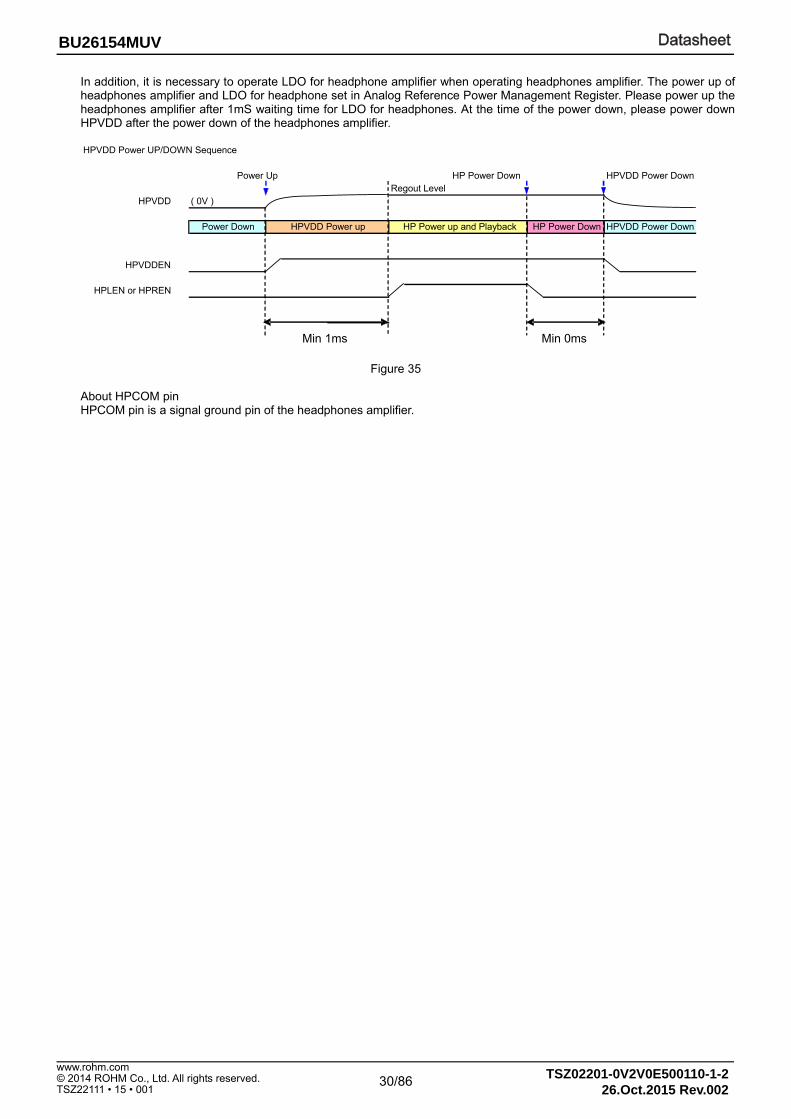
In addition, it is necessary to operate LDO for headphone amplifier when operating headphones amplifier. The power up of headphones amplifier and LDO for headphone set in Analog Reference Power Management Register. Please power up the headphones amplifier after 1mS waiting time for LDO for headphones. At the time of the power down, please power down HPVDD after the power down of the headphones amplifier.
Figure 35
About HPCOM pin HPCOM pin is a signal ground pin of the headphones amplifier.
HPVDD Power UP/DOWN Sequence
Power Up HP Power Down HPVDD Power DownRegout Level
HPVDD ( 0V )
HPVDD Power Down
HPVDDEN
HPLEN or HPREN
HP Power DownHPVDD Power upPower Down HP Power up and Playback
Min 1ms Min 0ms

DatasheetDatasheet
31/86 TSZ02201-0V2V0E500110-1-2© 2014 ROHM Co., Ltd. All rights reserved.
26.Oct.2015 Rev.002
www.rohm.com
TSZ22111 • 15 • 001
BU26154MUV
Microphone amplifier The microphone input can support two modes, a single-end and differential. When using it in single-end input, it writes "0" in the MINDIF bit of the MIC Interface Control register. When using differential input, it writes "1". In the case of single-end input, it can input from MINP pin or MINN pin. Please set of the input pin in MIC Select Control Register. Microphone bias The Case of using Microphone bias, it shows a recommended connection diagram. By all means, please connect a condenser (2.2uF at the minimum) to MBIASCAP outside pin. On this occasion, the LSI can improve noise characteristics by connecting the option resistance on the chart below (the optional resistance is up to 50 Ω).
Figure 36
In addition, according to the capacity of the outside condenser, it is necessary to wait until microphone bias is stable. In waiting time of MICBIAS, please set the value of the MICTIME bit at the MIC Input Charging Time register.
MBIASCAP
MicBiasAmplifierBU26154
option
2.2uF
DatasheetDatasheet
32/86 TSZ02201-0V2V0E500110-1-2© 2014 ROHM Co., Ltd. All rights reserved.
26.Oct.2015 Rev.002
www.rohm.com
TSZ22111 • 15 • 001
BU26154MUV
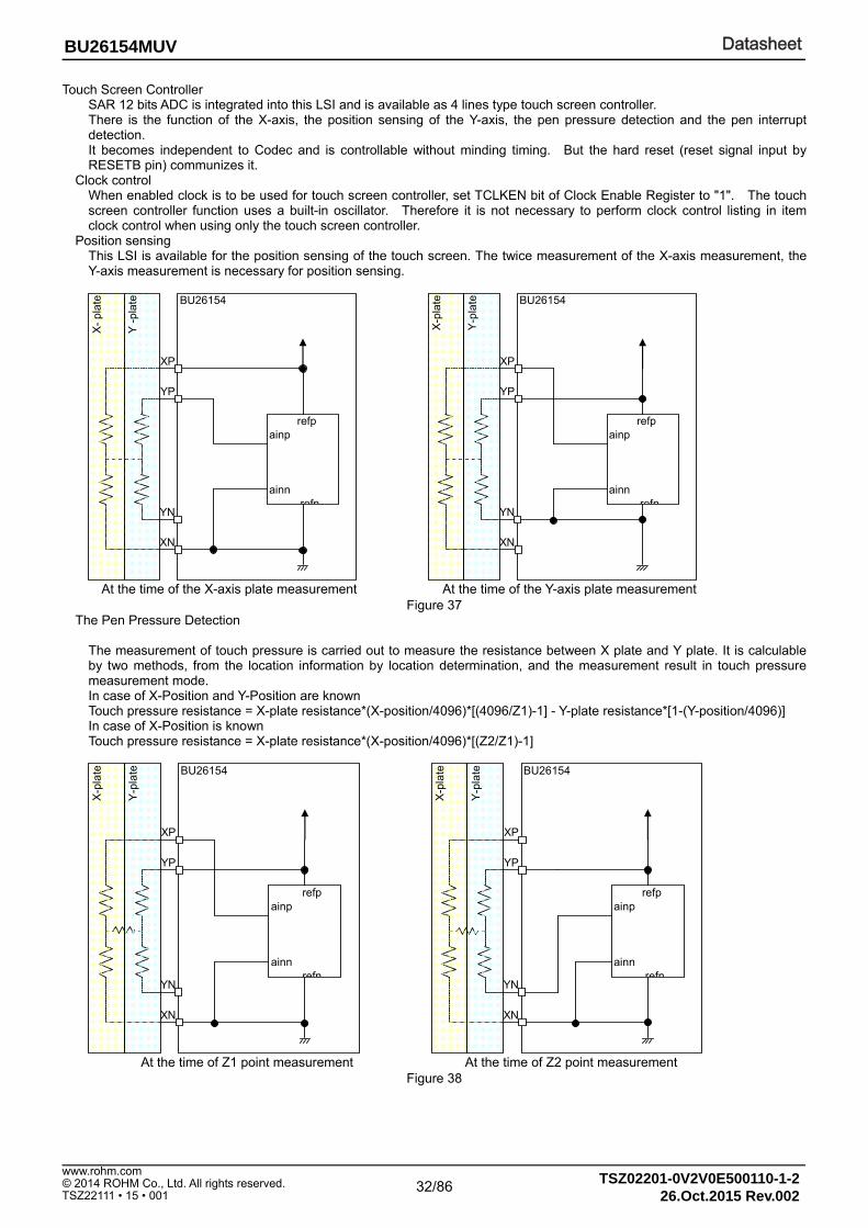
Touch Screen Controller SAR 12 bits ADC is integrated into this LSI and is available as 4 lines type touch screen controller. There is the function of the X-axis, the position sensing of the Y-axis, the pen pressure detection and the pen interrupt detection. It becomes independent to Codec and is controllable without minding timing. But the hard reset (reset signal input by RESETB pin) communizes it.
Clock control When enabled clock is to be used for touch screen controller, set TCLKEN bit of Clock Enable Register to "1". The touch screen controller function uses a built-in oscillator. Therefore it is not necessary to perform clock control listing in item clock control when using only the touch screen controller.
Position sensing This LSI is available for the position sensing of the touch screen. The twice measurement of the X-axis measurement, the Y-axis measurement is necessary for position sensing.
BU26154
refpainp
ainnrefn
YP
XP
YN
XN
X-
pla
te
Y -
pla
te BU26154
refpainp
ainnrefn
YP
XP
YN
XN
X-p
late
Y-p
late
At the time of the X-axis plate measurement At the time of the Y-axis plate measurement
Figure 37 The Pen Pressure Detection
The measurement of touch pressure is carried out to measure the resistance between X plate and Y plate. It is calculable by two methods, from the location information by location determination, and the measurement result in touch pressure measurement mode. In case of X-Position and Y-Position are known Touch pressure resistance = X-plate resistance*(X-position/4096)*[(4096/Z1)-1] - Y-plate resistance*[1-(Y-position/4096)] In case of X-Position is known Touch pressure resistance = X-plate resistance*(X-position/4096)*[(Z2/Z1)-1]
BU26154
refpainp
ainnrefn
YP
XP
YN
XN
X-p
late
Y-p
late BU26154
refpainp
ainnrefn
YP
XP
YN
XN
X-p
late
Y-p
late
At the time of Z1 point measurement At the time of Z2 point measurement
Figure 38
DatasheetDatasheet
33/86 TSZ02201-0V2V0E500110-1-2© 2014 ROHM Co., Ltd. All rights reserved.
26.Oct.2015 Rev.002
www.rohm.com
TSZ22111 • 15 • 001
BU26154MUV
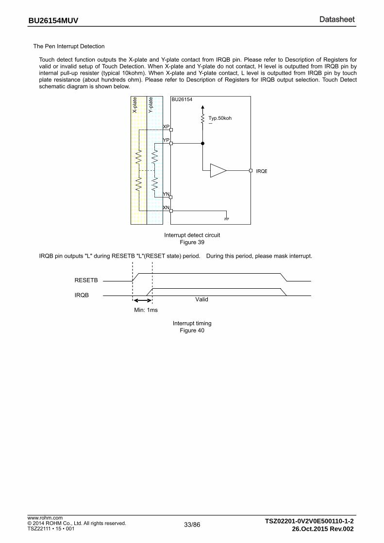
The Pen Interrupt Detection
Touch detect function outputs the X-plate and Y-plate contact from IRQB pin. Please refer to Description of Registers for valid or invalid setup of Touch Detection. When X-plate and Y-plate do not contact, H level is outputted from IRQB pin by internal pull-up resister (typical 10kohm). When X-plate and Y-plate contact, L level is outputted from IRQB pin by touch plate resistance (about hundreds ohm). Please refer to Description of Registers for IRQB output selection. Touch Detect schematic diagram is shown below.
BU26154
YP
XP
YN
XN
X-p
late
Y-p
late
IRQB
Typ.50kohm
Interrupt detect circuit Figure 39
IRQB pin outputs "L" during RESETB "L"(RESET state) period. During this period, please mask interrupt.
Interrupt timing
Figure 40
RESETB
IRQB Valid
Min: 1ms
DatasheetDatasheet
34/86 TSZ02201-0V2V0E500110-1-2© 2014 ROHM Co., Ltd. All rights reserved.
26.Oct.2015 Rev.002
www.rohm.com
TSZ22111 • 15 • 001
BU26154MUV
About Touch Panel Interface at Interrupt Wait Touch panel interface can switch to low power consumption by stopping the operation of unnecessary circuits at interrupt wait.
Setting of touch panel interface at interrupt wait 0x2d = 0x00, // Thermal detect circuit Disable 0x1d = 0x02, // MAPCON=2 0x05 = 0x22, // Level shifter for headphone OFF 0x13 = 0x00, // Reference current circuit for audio system OFF 0x1d = 0x00, // MAPCON=0 0x0d = 0x80, // Touch panel interface oscillation circuit Enable 0x1d = 0x01, // MAPCON=1 0x61 = 0x38, // Touch panel interface interrupt circuit Enable 0x1d = 0x00, // MAPCON=0 0x0d = 0x00, // Touch panel interface oscillation circuit Disable This state is interrupt wait mode. Please use a touch panel interface after interrupt, setting enable oscillation circuit. Please, set circuit from Disable to Enable in circuit when using of audio system function Setting at using of audio system function 0x2d = 0x01, // Thermal detect circuit Enable 0x1d = 0x02, // MAPCON=2 0x05 = 0x26, // Level shifter for headphone ON 0x13 = 0x01, // Reference current circuit for audio system ON 0x1d = 0x00, // MAPCON=0

DatasheetDatasheet
35/86 TSZ02201-0V2V0E500110-1-2© 2014 ROHM Co., Ltd. All rights reserved.
26.Oct.2015 Rev.002
www.rohm.com
TSZ22111 • 15 • 001
BU26154MUV
Operating Mode Normal operating mode It becomes Normal operating mode by setting Touch ADC Control registerTCHA2=0x1. Next AD conversion starts by reading register value of ADCR1 register (8Bit mode) or ADCR2 register (12Bit mode), at Normal operating mode.
TCLKEN Bit
Internal Clk
I2C Operation Write Data reception Slave address receptio Read Data reception
INDEX=0x61,TCHEN="1" INDEX=0x64
SCL
SDA D2 D1 D0 ACK 1 0 R ACK D7 D6 D5
Internal ADC Start Sync
ADC Status IDLE Data Hold AD Conversion1_1 AD Conversion1_2 IDLE Data Hold AD Conversion2_1 AD Conversion2_2 IDLE
ADCR1Register Data Valid1_1 Data Valid2_1
ADCR2 Register Data Valid1_2 Data Valid2_2
Tw_ADC1 Tw_ADC1
Tw_ADC2 Tw_ADC2 12Bit Normal Mode I2C Timing
TCLKEN Bit
Internal Clk
I2C Operation Write Data reception Slave address receptio Read Data reception
INDEX=0x61,TCHEN="1" INDEX=0x62
SCL
SDA D2 D1 D0 ACK 1 0 R ACK D7 D6 D5
Internal ADC Start Sync
ADC Status IDLE Data Hold AD Conversion1 IDLE Data Hold AD Conversion2 IDLE
ADCR1Register Data Valid1 Data Valid2
ADCR2 Register
Tw_ADC1 Tw_ADC1 8Bit Normal Mode I2C Timing
AD conversion starts by rising edge of CSB at using SPI. 12Bit timing mode chart is listed below. 8Bit mode start timing is similar it.
TCLKEN Bit
Internal Clk
SPI Operation Write Data Read Data
INDEX=0x61,TCHEN="1" INDEX = 0x64
SCLK
CSB
Internal ADC Start Sync
ADC Status IDLE Data Hold AD Conversion1_1 AD Conversion1_2 IDLE Data Hold AD Conversion2_1 AD Conversion2_2 Idle
ADCR1Register Data Valid1_1 Data Valid2_1
ADCR2 Register Data Valid1_2 Data Valid2_2
Tw_ADC1 Tw_ADC1
Tw_ADC2 Tw_ADC2 8Bit Normal Mode SPI Timing

DatasheetDatasheet
36/86 TSZ02201-0V2V0E500110-1-2© 2014 ROHM Co., Ltd. All rights reserved.
26.Oct.2015 Rev.002
www.rohm.com
TSZ22111 • 15 • 001
BU26154MUV
Auto Operation Mode When TCHA2 bit of Touch ADC Control register is set to "0", BU26154MUV is set to Auto Operation Mode. When is to set in Auto Mode Operation, BU 26154 MUV is Interrupt mode by reading to ADCR2 register in 12 bit mode and BU 26154 MUV is Interrupt mode by reading to ADCR1 register in 8 bit mode.
TCLKEN Bit
Internal Clk
I2C Operation Write Data reception Slave address receptio Read Data reception
INDEX=0x61,TCHEN="1" INDEX=0x64
SCL
SDA D2 D1 D0 ACK 1 0 R ACK D7 D6 D5
Internal ADC Start Sync
ADC Status IDLE Data Hold AD Conversion1_1 AD Conversion1_2 IDLE Interrupt Mode
ADCR1Register Data Valid1_1
ADCR2 Register Data Valid1_2
Tw_ADC1
Tw_ADC2 12Bit Auto Mode I2C Timing
TCLKEN Bit
Internal Clk
I2C Operation Write Data reception Slave address receptio Read Data reception
INDEX=0x61,TCHEN="1" INDEX=0x62
SCL
SDA D2 D1 D0 ACK 1 0 R ACK D7 D6 D5
Internal ADC Start Sync
ADC Status IDLE Data Hold AD Conversion1_1 IDLE Interrupt Mode
ADCR1Register Data Valid1_1
ADCR2 Register
Tw_ADC1 8Bit Auto Mode I2C Timing
TCLKEN Bit
Internal Clk
SPI Operation Write Data Read Data
INDEX=0x61,TCHEN="1" INDEX = 0x64
SCLK
CSB
Internal ADC Start Sync
ADC Status IDLE Data Hold AD Conversion1_1 AD Conversion1_2 IDLE Interrupt Mode
ADCR1Register Data Valid1_1
ADCR2 Register Data Valid1_2
Tw_ADC1
Tw_ADC2 12Bit Auto Mode SPI Timing
DatasheetDatasheet
37/86 TSZ02201-0V2V0E500110-1-2© 2014 ROHM Co., Ltd. All rights reserved.
26.Oct.2015 Rev.002
www.rohm.com
TSZ22111 • 15 • 001
BU26154MUV
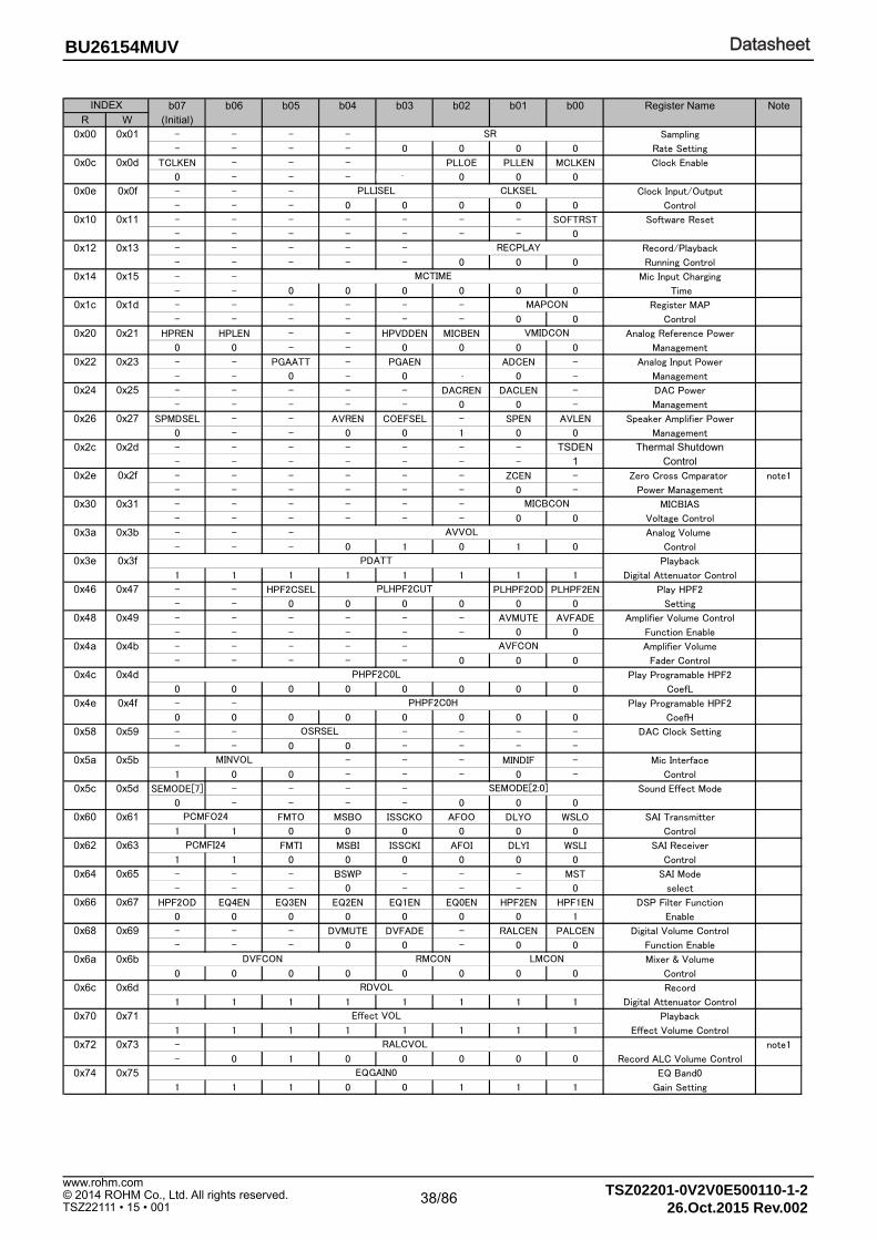
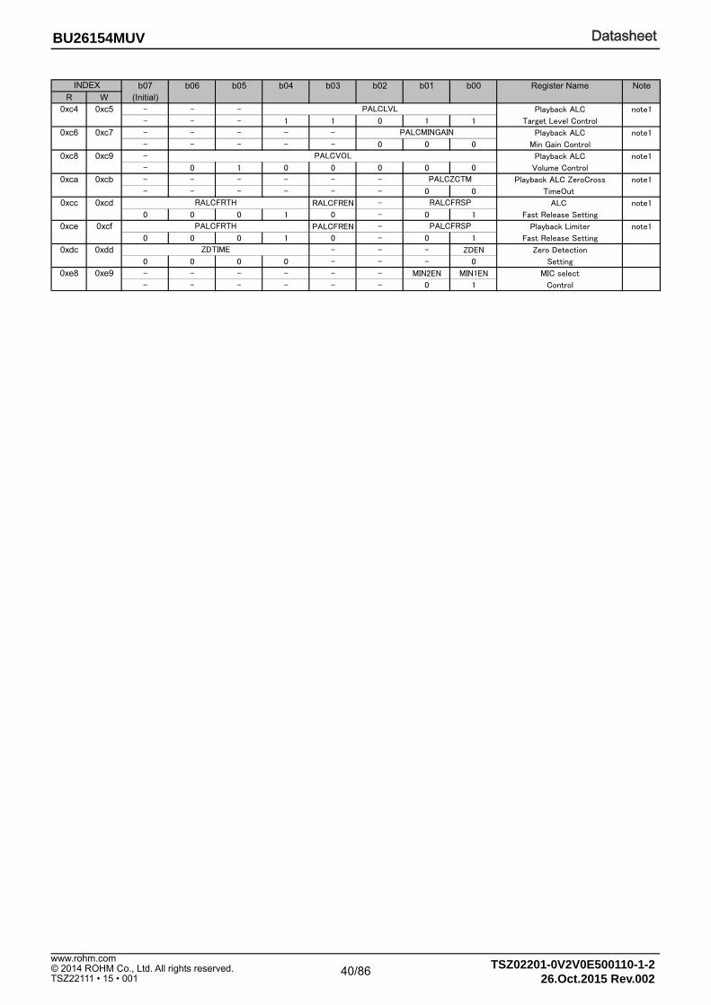
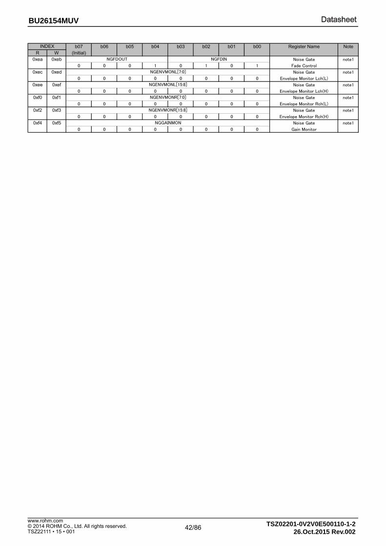
Register function explanation Register map Note: “-” indicates a reserved bit. They return “0” for read. Write “0” to the bit every time. If “1” is written to this bit, the operations cannot be guaranteed. Don’t write data to empty INDEX or register bit to guarantee normal operation. A function with (*)bit doesn’t need internal clock to change state.
The following registers are accessible at the time of MAPCON=0x0 of the Register Map Control register (0x1c/0x1d).
DatasheetDatasheet
38/86 TSZ02201-0V2V0E500110-1-2© 2014 ROHM Co., Ltd. All rights reserved.
26.Oct.2015 Rev.002
www.rohm.com
TSZ22111 • 15 • 001
BU26154MUV
b07 b06 b05 b04 b03 b02 b01 b00 Register Name Note
R W (Initial)0x00 0x01 - - - - Sampling
- - - - 0 0 0 0 Rate Setting
0x0c 0x0d TCLKEN - - - MCLKOE PLLOE PLLEN MCLKEN Clock Enable
0 - - - 0 0 0 0
0x0e 0x0f - - - Clock Input/Output
- - - 0 0 0 0 0 Control
0x10 0x11 - - - - - - - SOFTRST Software Reset
- - - - - - - 0
0x12 0x13 - - - - - Record/Playback
- - - - - 0 0 0 Running Control
0x14 0x15 - - Mic Input Charging
- - 0 0 0 0 0 0 Time
0x1c 0x1d - - - - - - Register MAP
- - - - - - 0 0 Control
0x20 0x21 HPREN HPLEN - - HPVDDEN MICBEN Analog Reference Power
0 0 - - 0 0 0 0 Management
0x22 0x23 - - PGAATT - PGAEN ADCREN ADCEN - Analog Input Power
- - 0 - 0 0 0 - Management
0x24 0x25 - - - - - DACREN DACLEN - DAC Power
- - - - - 0 0 - Management
0x26 0x27 SPMDSEL - - AVREN COEFSEL - SPEN AVLEN Speaker Amplifier Power
0 - - 0 0 1 0 0 Management
0x2c 0x2d - - - - - - - TSDEN Thermal Shutdown- - - - - - - 1 Control
0x2e 0x2f - - - - - - ZCEN - Zero Cross Cmparator note1
- - - - - - 0 - Power Management
0x30 0x31 - - - - - - MICBIAS
- - - - - - 0 0 Voltage Control
0x3a 0x3b - - - Analog Volume
- - - 0 1 0 1 0 Control
0x3e 0x3f Playback
1 1 1 1 1 1 1 1 Digital Attenuator Control
0x46 0x47 - - HPF2CSEL PLHPF2OD PLHPF2EN Play HPF2
- - 0 0 0 0 0 0 Setting
0x48 0x49 - - - - - - AVMUTE AVFADE Amplifier Volume Control
- - - - - - 0 0 Function Enable
0x4a 0x4b - - - - - Amplifier Volume
- - - - - 0 0 0 Fader Control
0x4c 0x4d Play Programable HPF2
0 0 0 0 0 0 0 0 CoefL
0x4e 0x4f - - Play Programable HPF2
0 0 0 0 0 0 0 0 CoefH
0x58 0x59 - - - - - - DAC Clock Setting
- - 0 0 - - - -
0x5a 0x5b - - - MINDIF - Mic Interface
1 0 0 - - - 0 - Control
0x5c 0x5d SEMODE[7] - - - - Sound Effect Mode
0 - - - - 0 0 0
0x60 0x61 FMTO MSBO ISSCKO AFOO DLYO WSLO SAI Transmitter
1 1 0 0 0 0 0 0 Control
0x62 0x63 FMTI MSBI ISSCKI AFOI DLYI WSLI SAI Receiver
1 1 0 0 0 0 0 0 Control
0x64 0x65 - - - BSWP - - - MST SAI Mode
- - - 0 - - - 0 select
0x66 0x67 HPF2OD EQ4EN EQ3EN EQ2EN EQ1EN EQ0EN HPF2EN HPF1EN DSP Filter Function
0 0 0 0 0 0 0 1 Enable
0x68 0x69 - - - DVMUTE DVFADE - RALCEN PALCEN Digital Volume Control
- - - 0 0 - 0 0 Function Enable
0x6a 0x6b Mixer & Volume
0 0 0 0 0 0 0 0 Control
0x6c 0x6d Record
1 1 1 1 1 1 1 1 Digital Attenuator Control
0x70 0x71 Playback
1 1 1 1 1 1 1 1 Effect Volume Control
0x72 0x73 - note1
- 0 1 0 0 0 0 0 Record ALC Volume Control
0x74 0x75 EQ Band0
1 1 1 0 0 1 1 1 Gain Setting
INDEX
SR
MCTIME
PLLISEL CLKSEL
RECPLAY
PDATT
MAPCON
VMIDCON
MICBCON
AVVOL
SEMODE[2:0]
PHPF2C0H
PHPF2C0L
PLHPF2CUT
AVFCON
PCMFO24
PCMFI24
DVFCON
OSRSEL
MINVOL
EQGAIN0
RALCVOL
Effect VOL
RMCON LMCON
RDVOL
-
-

DatasheetDatasheet
39/86 TSZ02201-0V2V0E500110-1-2© 2014 ROHM Co., Ltd. All rights reserved.
26.Oct.2015 Rev.002
www.rohm.com
TSZ22111 • 15 • 001
BU26154MUV
b07 b06 b05 b04 b03 b02 b01 b00 Register Name Note
R W (Initial)0x76 0x77 EQ Band1
1 1 1 0 0 1 1 1 Gain Setting
0x78 0x79 EQ Band2
1 1 1 0 0 1 1 1 Gain Setting
0x7a 0x7b EQ Band3
1 1 1 0 0 1 1 1 Gain Setting
0x7c 0x7d EQ Band4
1 1 1 0 0 1 1 1 Gain Setting
0x7e 0x7f - - - - - High Pass Filter2
- - - - - 0 0 0 Cut-off Control
0x80 0x81 Programable Equalizer Band0
0 0 0 0 0 0 0 0 Coefficient-a0 (L)
0x82 0x83 Programable Equalizer Band0
0 0 0 0 0 0 0 0 Coefficient-a0 (H)
0x84 0x85 Programable Equalizer Band0
0 0 0 0 0 0 0 0 Coefficient-a1 (L)
0x86 0x87 Programable Equalizer Band0
0 0 0 0 0 0 0 0 Coefficient-a1 (H)
0x88 0x89 Programable Equalizer Band1
0 0 0 0 0 0 0 0 Coefficient-a0 (L)
0x8a 0x8b Programable Equalizer Band1
0 0 0 0 0 0 0 0 Coefficient-a0 (H)
0x8c 0x8d Programable Equalizer Band1
0 0 0 0 0 0 0 0 Coefficient-a1 (L)
0x8e 0x8f Programable Equalizer Band1
0 0 0 0 0 0 0 0 Coefficient-a1 (H)
0x90 0x91 Programable Equalizer Band2
0 0 0 0 0 0 0 0 Coefficient-a0 (L)
0x92 0x93 Programable Equalizer Band2
0 0 0 0 0 0 0 0 Coefficient-a0 (H)
0x94 0x95 Programable Equalizer Band2
0 0 0 0 0 0 0 0 Coefficient-a1 (L)
0x96 0x97 Programable Equalizer Band2
0 0 0 0 0 0 0 0 Coefficient-a1 (H)
0x98 0x99 Programable Equalizer Band3
0 0 0 0 0 0 0 0 Coefficient-a0 (L)
0x9a 0x9b Programable Equalizer Band3
0 0 0 0 0 0 0 0 Coefficient-a0 (H)
0x9c 0x9d Programable Equalizer Band3
0 0 0 0 0 0 0 0 Coefficient-a1 (L)
0x9e 0x9f Programable Equalizer Band3
0 0 0 0 0 0 0 0 Coefficient-a1 (H)
0xa0 0xa1 Programable Equalizer Band4
0 0 0 0 0 0 0 0 Coefficient-a0 (L)
0xa2 0xa3 Programable Equalizer Band4
0 0 0 0 0 0 0 0 Coefficient-a0 (H)
0xa4 0xa5 Programable Equalizer Band4
0 0 0 0 0 0 0 0 Coefficient-a1 (L)
0xa6 0xa7 Programable Equalizer Band4
0 0 0 0 0 0 0 0 Coefficient-a1 (H)
0xb2 0xb3 - - - - Record ALC note1
- - - - 0 0 1 0 Attack Time Control
0xb4 0xb5 - - - - Record ALC note1
- - - - 0 0 1 1 Decay Time Control
0xb8 0xb9 - - - Record ALC note1
- - - 1 0 1 1 1 Target Level Control
0xba 0xbb - - - - - Record ALC note1
- - - - - 0 0 0 Min Gain Control
0xbc 0xbd RSATEN Record ALC
0 0 1 0 0 0 1 0 Satulation Detect Control
0xbe 0xbf - - - - - - Record ALC Zero Cross note1
- - - - - - 0 0 Time Out Control
0xc0 0xc1 - - - - Playback ALC note1
- - - - 0 1 0 0 Attack Time Control
0xc2 0xc3 - - - - Playback ALC note1
- - - - 0 1 0 1 Decay Time Control
EQGAIN4
EQGAIN3
EQGAIN2
INDEX
EQGAIN1
EQ0A1L
EQ0A0H
HPF2CUT
EQ0A0L
EQ1A1L
EQ1A0H
EQ1A0L
EQ0A1H
EQ2A1L
EQ2A0H
EQ2A0L
EQ1A1H
EQ3A1L
EQ3A0H
EQ3A0L
EQ2A1H
EQ4A1L
EQ4A0H
EQ4A0L
EQ3A1H
RALCLVL
RALCATK
RALCDCY
EQ4A1H
RALCZCTM
PALCATK
RALCMINGAIN
RSATMINGAIN
PALCDCY
DatasheetDatasheet
40/86 TSZ02201-0V2V0E500110-1-2© 2014 ROHM Co., Ltd. All rights reserved.
26.Oct.2015 Rev.002
www.rohm.com
TSZ22111 • 15 • 001
BU26154MUV
b07 b06 b05 b04 b03 b02 b01 b00 Register Name Note
R W (Initial)0xc4 0xc5 - - - Playback ALC note1
- - - 1 1 0 1 1 Target Level Control
0xc6 0xc7 - - - - - Playback ALC note1
- - - - - 0 0 0 Min Gain Control
0xc8 0xc9 - Playback ALC note1
- 0 1 0 0 0 0 0 Volume Control
0xca 0xcb - - - - - - Playback ALC ZeroCross note1
- - - - - - 0 0 TimeOut
0xcc 0xcd RALCFREN - ALC note1
0 0 0 1 0 - 0 1 Fast Release Setting
0xce 0xcf PALCFREN - Playback Limiter note1
0 0 0 1 0 - 0 1 Fast Release Setting
0xdc 0xdd - - - ZDEN Zero Detection
0 0 0 0 - - - 0 Setting
0xe8 0xe9 - - - - - - MIN2EN MIN1EN MIC select
- - - - - - 0 1 Control
INDEX
PALCMINGAIN
PALCVOL
PALCLVL
PALCFRTH PALCFRSP
PALCZCTM
RALCFRTH RALCFRSP
ZDTIME

DatasheetDatasheet
41/86 TSZ02201-0V2V0E500110-1-2© 2014 ROHM Co., Ltd. All rights reserved.
26.Oct.2015 Rev.002
www.rohm.com
TSZ22111 • 15 • 001
BU26154MUV
The following registers are accessible at the time of MAPCON=0x1 of the Register Map Control register (0x1c/0x1d). b07 b06 b05 b04 b03 b02 b01 b00 Register Name Note
R W (Initial)0x02 0x03 - - - - - FPLL M setting
- - - - - 0 0 0
0x04 0x05 FPLL N Setting(L)
0 0 0 0 0 0 0 0
0x06 0x07 - - - - - - - FPLLNH FPLL N Setting(H)
- - - - - - - 0
0x08 0x09 - - - FPLL D Setting
- - - 0 0 0 0 0
0x0a 0x0b FPLL F Setting(L)
0 0 0 0 0 0 0 0
0x0c 0x0d FPLL F Setting(H)
0 0 0 0 0 0 0 0
0x0e 0x0f FPLL F_D Setting(L)
0 0 0 0 0 0 0 0
0x10 0x11 FPLL F_D Setting(H)
0 0 0 0 0 0 0 0
0x12 0x13 - - - - FPLL V setting
- - - - 0 0 0 0
0x1c 0x1d - - - - - - RegisterMAP
- - - - - - 0 0 Control
0x20 0x21 - - - - - - - SCEN Soft Clip Enable
- - - - - - - 0
0x22 0x23 - Soft Clip Threshold H
- 0 0 0 0 0 0 0
0x24 0x25 Soft Clip Threshold M
0 0 0 0 0 0 0 0
0x26 0x27 Soft Clip Threshold L
0 0 0 0 0 0 0 0
0x28 0x29 - - - - - Soft Clip Gain
- - - - - 0 0 1
0x60 0x61 TCHSEN TCHA2 TCHA1 TCHA0 - TCHRSEL TCHMODE - Touch ADC Control
0 1 1 1 1 0 0 -
0x62 0x63 Touch ADC result1
0 0 0 0 0 0 0 0
0x64 0x65 - - - - Touch ADC result2
0 0 0 0 - - - -
0x82 0x83 - - HPRIN2EN HPRIN1EN - - - HPLIN1EN Headphone input
- - 0 0 - - - 0 Select Control
0x84 0x85 - - - - SPIN2EN SPIN1EN SPAMP input Control
- - - - 0 0 0 0
0xa0 0xa1 - - - - - - PLPFOD PLPFEN Play Programable LPF
- - - - - - 0 0 Setting
0xa2 0xa3 Play Programable LPF
0 0 0 0 0 0 0 0 Coef (L)
0xa4 0xa5 Play Programable LPF
0 0 0 0 0 0 0 0 Coef (H)
0xa6 0xa7 - - - - - - RLPFOD RLPFEN Rec Programable LPF
- - - - - - 0 0 Setting
0xa8 0xa9 Rec Programable LPF
0 0 0 0 0 0 0 0 Coef (L)
0xaa 0xab Rec Programable LPF
0 0 0 0 0 0 0 0 Coef (H)
0xda 0xdb - - - - - - - NGEN Noise Gate Setting note1
- - - - - - - 0
0xde 0xdf Noise Gate note1
1 1 0 1 0 0 1 1 Minimum Gain
0xe0 0xe1 - - Noise Gate note1
- - 0 1 0 0 1 0 Threshold
0xe2 0xe3 - - - - - Noise Gate note1
- - - - - 0 1 0 Threshold Hysteresis
0xe4 0xe5 - Noise Gate note1
- 0 0 1 0 1 0 0 Slope
0xe6 0xe7 - - - - - - Noise Gate note1
- - - - - - 1 0 Gain Step
0xe8 0xe9 - - Noise Gate note1
- 0 0 1 - 0 0 0 Time Setting
FPLLM
FPLLNL
INDEX
FPLLFDL
FPLLFH
FPLLFL
FPLLD
SCTHRH
FPLLV
MAPCON
FPLLFDH
SCGAIN
ADCR1
SCTHRL
SCTHRM
PLPFC0H
PLPFC0L
ADCR2
SPVOL
NGTH
NGMINGAIN
RLPFC0H
RLPFC0L
NGGAINSTEP
NGENVAVE NGZTIM
NGTHHYS
NGSLOPE
DatasheetDatasheet
42/86 TSZ02201-0V2V0E500110-1-2© 2014 ROHM Co., Ltd. All rights reserved.
26.Oct.2015 Rev.002
www.rohm.com
TSZ22111 • 15 • 001
BU26154MUV
b07 b06 b05 b04 b03 b02 b01 b00 Register Name Note
R W (Initial)0xea 0xeb Noise Gate note1
0 0 0 1 0 1 0 1 Fade Control
0xec 0xed Noise Gate note1
0 0 0 0 0 0 0 0 Envelope Monitor Lch(L)
0xee 0xef Noise Gate note1
0 0 0 0 0 0 0 0 Envelope Monitor Lch(H)
0xf0 0xf1 Noise Gate note1
0 0 0 0 0 0 0 0 Envelope Monitor Rch(L)
0xf2 0xf3 Noise Gate note1
0 0 0 0 0 0 0 0 Envelope Monitor Rch(H)
0xf4 0xf5 Noise Gate note1
0 0 0 0 0 0 0 0 Gain Monitor
NGFDIN
NGENVMONL[7:0]
INDEX
NGFDOUT
NGGAINMON
NGENVMONR[15:8]
NGENVMONR[7:0]
NGENVMONL[15:8]

DatasheetDatasheet
43/86 TSZ02201-0V2V0E500110-1-2© 2014 ROHM Co., Ltd. All rights reserved.
26.Oct.2015 Rev.002
www.rohm.com
TSZ22111 • 15 • 001
BU26154MUV
The following registers are accessible at the time of MAPCON=0x2 of the Register Map Control register (0x1c/0x1d). b07 b06 b05 b04 b03 b02 b01 b00 Register Name Note
R W (Initial)0x00 0x01 - - - - - - - EXMODE PLL External Components
- - - - - - - 1 Setting Register
0x04 0x05 - - - - - HPLSEN - - Audio Analog
- - 1 - - 1 1 - Control2
0x12 0x13 - - - - - - - AREFI1EN Audio Analog - - - - - - - 1 Contrl1
0x1c 0x1d - - - - - - RegisterMAP
- - - - - - 0 0 Control
0x24 0x25 P2 Bass+ Parameter0A0 0 0 0 0 0 0 0
0x26 0x27 - P2 Bass+ Parameter1A- 0 0 0 0 0 0 0
0x28 0x29 P2 Bass+ Parameter2A0 0 0 0 0 0 0 0
0x2a 0x2b P2 Bass+ Parameter0B0 0 0 0 0 0 0 0
0x2c 0x2d - P2 Bass+ Parameter1B- 0 0 0 0 0 0 0
0x2e 0x2f P2 Bass+ Parameter2B0 0 0 0 0 0 0 0
0x04 0x05 - - - - - HPLSEN - - Audio Analog
- - 1 - - 1 1 - Control2
0x12 0x13 - - - - - - - AREFI1EN Audio Analog - - - - - - - 1 Contrl1
0x1c 0x1d - - - - - - RegisterMAP
- - - - - - 0 0 Control
0x46 0x47 - - HPF2CSELB PLHPF2ODB PLHPF2ENB Play HPF2B
- - 0 0 0 0 0 0
0x4c 0x4d Play Programable HPF2
0 0 0 0 0 0 0 0 CoefL B
0x4e 0x4f - - Play Programable HPF2
0 0 0 0 0 0 0 0 CoefH B
0x5c 0x5d SEMODE[7] - - - - Sound Effect Mode B
0 - - - - 0 0 0
0x66 0x67 HPF2ODB EQ4ENB EQ3ENB EQ2ENB EQ1ENB EQ0ENB HPF2ENB HPF1ENB Filter Func
0 0 0 0 0 0 0 1 Enable B
0x70 0x71 Playback
1 1 1 1 1 1 1 1 Effect Volume Control B
0x72 0x73 Playback
1 1 1 1 1 1 1 1 Digital Attenuator Control B
0x74 0x75 EQ gain
1 1 1 0 0 1 1 1 Band0 B
0x76 0x77 EQ gain
1 1 1 0 0 1 1 1 Band1 B
0x78 0x79 EQ gain
1 1 1 0 0 1 1 1 Band2 B
0x7a 0x7b EQ gain
1 1 1 0 0 1 1 1 Band3 B
0x7c 0x7d EQ gain
1 1 1 0 0 1 1 1 Band4 B
0x7e 0x7f EQ Band0
0 0 0 0 0 0 0 0 Coef0L B
0x80 0x81 EQ Band0
0 0 0 0 0 0 0 0 Coef0H B
0x82 0x83 EQ Band0
0 0 0 0 0 0 0 0 Coef1L B
0x84 0x85 EQ Band0
0 0 0 0 0 0 0 0 Coef1H B
0x86 0x87 EQ Band1
0 0 0 0 0 0 0 0 Coef0L B
0x88 0x89 EQ Band1
0 0 0 0 0 0 0 0 Coef0H B
0x8a 0x8b EQ Band1
0 0 0 0 0 0 0 0 Coef1L B
0x8c 0x8d EQ Band1
0 0 0 0 0 0 0 0 Coef1H B
0x8e 0x8f EQ Band2
0 0 0 0 0 0 0 0 Coef0L B
0x90 0x91 EQ Band2
0 0 0 0 0 0 0 0 Coef0H B
0x92 0x93 EQ Band2
0 0 0 0 0 0 0 0 Coef1L B
0x94 0x95 EQ Band2
0 0 0 0 0 0 0 0 Coef1H B
0x96 0x97 EQ Band3
0 0 0 0 0 0 0 0 Coef0L B
MAPCON
P2BHPF1B
P2BGAINBSB P2BLPF2B
P2BGAINEVB P2BGAINODB
EQ3A0LB
EQ2A1HB
EQ2A1LB
EQ2A0HB
EQ2A0LB
EQ1A1HB
EQ1A1LB
EQ1A0HB
EQ1A0LB
EQ0A1HB
EQ0A1LB
EQ0A0HB
EQ0A0LB
EQGAIN4B
EQGAIN3B
EQGAIN2B
EQGAIN1B
EQGAIN0B
PDATTB
SEMODE[2:0]
Effect VOLB
PHPF2C0HB
PLHPF2CUTB
PHPF2C0LB
P2BLPF1A
INDEX
MAPCON
P2BHPF1A
P2BGAINBSA P2BLPF2A
P2BGAINEVA P2BGAINODA
P2BLPF1B

DatasheetDatasheet
44/86 TSZ02201-0V2V0E500110-1-2© 2014 ROHM Co., Ltd. All rights reserved.
26.Oct.2015 Rev.002
www.rohm.com
TSZ22111 • 15 • 001
BU26154MUV
b07 b06 b05 b04 b03 b02 b01 b00 Register Name NoteR W (Initial)
0x98 0x99 EQ Band3
0 0 0 0 0 0 0 0 Coef0H B
0x9a 0x9b EQ Band3
0 0 0 0 0 0 0 0 Coef1L B
0x9c 0x9d EQ Band3
0 0 0 0 0 0 0 0 Coef1H B
0x9e 0x9f EQ Band4
0 0 0 0 0 0 0 0 Coef0L B
0xa0 0xa1 EQ Band4
0 0 0 0 0 0 0 0 Coef0H B
0xa2 0xa3 EQ Band4
0 0 0 0 0 0 0 0 Coef1L B
0xa4 0xa5 EQ Band4
0 0 0 0 0 0 0 0 Coef1H B
EQ4A1HB
EQ4A1LB
EQ4A0HB
EQ4A0LB
EQ3A1HB
EQ3A1LB
INDEX
EQ3A0HB

DatasheetDatasheet
45/86 TSZ02201-0V2V0E500110-1-2© 2014 ROHM Co., Ltd. All rights reserved.
26.Oct.2015 Rev.002
www.rohm.com
TSZ22111 • 15 • 001
BU26154MUV
Register details explanation Note: “-” indicates a reserved bit. They return “0” for read. Write “0” to the bit every time. If “1” is written to this bit, the operations cannot be guaranteed. Don’t write data to empty INDEX or register bit to guarantee normal operation. A function with (*)bit doesn’t need internal clock to change state.
Sampling Rate Setting Register
MAPCON b07 b06 b05 b04 b03 b02 b01 b00R W (Initial)
0x0 0x00 0x01 - - - -
- - - - 0 0 0 0
INDEX
SR
This register sets the sampling rate of the recording/playback. Please perform the change of this register level in RECPLAY=0x0) at a recording/playback stop.
SR [3:0]
Setting Explanation 0x0 8kHz 0x1 11.025 kHz 0x2 12kHz 0x3 16kHz 0x4 22.05 kHz 0x5 24kHz 0x6 32kHz 0x7 44.1 kHz 0x8 48kHz
Clock Enable Register
MAPCON b07 b06 b05 b04 b03 b02 b01 b00R W (Initial)
0x0 0x0c 0x0d TCLKEN - - - - PLLOE PLLEN MCLKEN
0 - - - - 0 0 0
INDEX
This register is a register to control the operation of the clock.
MCLKEN
This bit sets permission / stop of the input of the MCLKI terminal. The input logic of the MCLKI terminal becomes invalid at the time of the stop and clock is not transmitted to the LSI inside.
Setting Explanation
0 MCLKI terminal input stop A clock stops at the input first grade of the terminal
1 MCLKI terminal input permission
PLLEN This bit sets movement / stop of PLL.
Setting Explanation 0 PLL stop 1 PLL movement
After setting the PLL Setting register, please set PLLEN bit to "1".
PLLOE This bit is to set the status of PLL output. Set this bit to “1” after PLL operation has stabilized. Also, this bit must be set to “1” if PLL is not used, otherwise internal clock cannot be provided.
Setting Explanation 0 The PLL output is put under ban 1 PLL output permission
TCLKEN
This bit sets the clock for the touch panel interface circuit. TCLKEN Explanation
0 Disable clock for the touch panel interface. 1 Enable clock for the touch panel interface.

DatasheetDatasheet
46/86 TSZ02201-0V2V0E500110-1-2© 2014 ROHM Co., Ltd. All rights reserved.
26.Oct.2015 Rev.002
www.rohm.com
TSZ22111 • 15 • 001
BU26154MUV
Clock Input / Output Control Register
MAPCON b07 b06 b05 b04 b03 b02 b01 b00
R W (Initial)
0x0 0x0e 0x0f - - -
- - - 0 0 0 0 0
INDEX
PLLISEL CLKSEL
This register is to select internal clock. It is to use or not use and to create MCLKI input or internal clock divided PLL.
CLKSEL[2:0] Choose a clock to be use
Setting Explanation
0x0 Using PLL lets you output 256fs clock from PLL. The PLL output is just used inside this LSI.
0x2 Using PLL lets you output 512fs clock from PLL. The clock that is divided by 1/2 the PLL output is used inside this LSI.
0x3 Using PLL lets you output 1024fs clock from PLL The clock that is divided by 1/4 the PLL output is used inside this LSI.
0x4 Input 256fs clock to MCLKI terminal and PLL is not used. MCLKI terminal input is just used in this LSI.
0x6 Input 512fs clock to MCLKI terminal and PLL is not used. The clock that is divided by ½ the MCLKI terminal input is used inside this LSI.
0x7 Input 1024fs clock than MCLKI terminal and use it without using PLL. The clock that is divided by 1/4 the MCLKI terminal input is used inside this LSI.
PLLISEL[1:0]
When this bit chooses to input clock into PLL and does not use PLL, please set register to 0x0. Setting Explanation
0x0 Prohibited from setting 0x1 Use MCLKI terminal input 0x2 Use BCLK terminal input
Software Reset Register
MAPCON b07 b06 b05 b04 b03 b02 b01 b00
R W (Initial)
0x0 0x10 0x11 - - - - - - - SOFTRST
- - - - - - - 0
INDEX
This register is for software reset. CPU interface and this register are reset by writing SOFTRST bit to “1”. And then, write “0” for releasing reset.
Record/Playback Running Control Register
MAPCON b07 b06 b05 b04 b03 b02 b01 b00
R W (Initial)
0x0 0x12 0x13 - - - - -
- - - - - 0 0 0
INDEX
RECPLAY
This register controls start / stop of the recording/playback operation of the LSI.
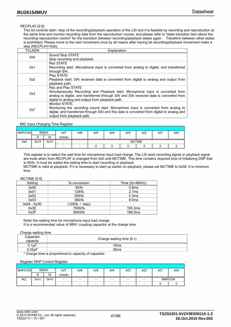
DatasheetDatasheet
47/86 TSZ02201-0V2V0E500110-1-2© 2014 ROHM Co., Ltd. All rights reserved.
26.Oct.2015 Rev.002
www.rohm.com
TSZ22111 • 15 • 001
BU26154MUV
RECPLAY [2:0] This bit controls start / stop of the recording/playback operation of the LSI and it is feasible by recording and reproduction at the same time and monitor recording data from the reproduction course, and please refer to "state transition item about the recording reproduction control" for the transition between recording/playback states again. Transition between other states is prohibited. Please move to the next movement once by all means after having let recording/playback movement make a stop (RECPLAY=0x0). TCLKEN Explanation
0x0 Sound Stop STATE Stop recording and playback.
0x1 Rec STATE Recording start. Microphone input is converted from analog to digital, and transferred through SAI.
0x2 Play STATE Playback start. SAI received data is converted from digital to analog and output from playback path.
0x3
Rec and Play STATE. Simultaneously Recording and Playback start. Microphone input is converted from analog to digital, and transferred through SAI and SAI received data is converted from digital to analog and output from playback path.
0x7
Monitor STATE. Monitoring the recording sound start. Microphone input is converted from analog to digital, and transferred through SAI and this data is converted from digital to analog and output from playback path.
MIC Input Charging Time Register
MAPCON b07 b06 b05 b04 b03 b02 b01 b00
R W (Initial)
0x0 0x14 0x15 - -
- - 0 0 0 0 0 0
INDEX
MCTIME
This register is to select the wait time for microphone input load charge. The LSI work recording signal or playback signal are mute when from RECPLAY is changed from 0x0 until MCTIME. This time contains required time of initializing DSP that is 40/fs. It must be waited the setting time to start recording or playback. MCTIME is valid at playback. If it is necessary to start up earlier on playback, please set MCTIME to 0x00. It is minimum time. .
MCTIME [5:0] Setting fs conversion Time (fs=48kHz) 0x00 40/fs 0.8ms 0x01 128/fs 2.7ms 0x02 256/fs 5.3ms 0x03 384/fs 8.0ms
0x04 - 0x3D (128/fs / step) : 0x3E 7936/fs 165.3ms 0x3F 8064/fs 168.0ms
Note) the waiting time for microphone input load charge It is a recommended value of MIN1 coupling capacitor at the charge time.
Charge waiting time
Capacitor capacity
Charge waiting time (6 τ)
0.1µF 16ms 0.22µF 36ms
* Charge time is proportional to capacity of capacitor.
Register MAP Control Register
MAPCON b07 b06 b05 b04 b03 b02 b01 b00
R W (Initial)
ALL 0x1c 0x1d - - - - - -
- - - - - - 0 0
INDEX
MAPCON
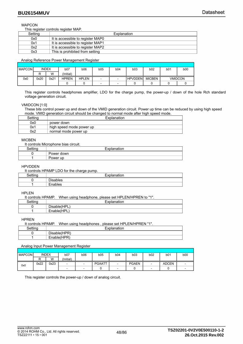
DatasheetDatasheet
48/86 TSZ02201-0V2V0E500110-1-2© 2014 ROHM Co., Ltd. All rights reserved.
26.Oct.2015 Rev.002
www.rohm.com
TSZ22111 • 15 • 001
BU26154MUV
MAPCON This register controls register MAP.
Setting Explanation 0x0 It is accessible to register MAP0 0x1 It is accessible to register MAP1 0x2 It is accessible to register MAP2 0x3 This is prohibited from setting
Analog Reference Power Management Register
MAPCON b07 b06 b05 b04 b03 b02 b01 b00
R W (Initial)
0x0 0x20 0x21 HPREN HPLEN - - HPVDDEN MICBEN
0 0 - - 0 0 0 0
INDEX
VMIDCON
This register controls headphones amplifier, LDO for the charge pump, the power-up / down of the hole Rch standard voltage generation circuit.
VMIDCON [1:0] These bits control power up and down of the VMID generation circuit. Power up time can be reduced by using high speed mode. VMID generation circuit should be changed to normal mode after high speed mode.
Setting Explanation 0x0 power down 0x1 high speed mode power up 0x2 normal mode power up
MICBEN
It controls Microphone bias circuit. Setting Explanation
0 Power down 1 Power up
HPVDDEN
It controls HPAMP LDO for the charge pump. Setting Explanation
0 Disables 1 Enables
HPLEN
It controls HPAMP. When using headphone, please set HPLEN/HPREN to "1". Setting Explanation
0 Disable(HPL) 1 Enable(HPL)
HPREN
It controls HPAMP. When using headphones , please set HPLEN/HPREN "1". Setting Explanation
0 Disable(HPR) 1 Enable(HPR)
Analog Input Power Management Register
MAPCON b07 b06 b05 b04 b03 b02 b01 b00R W (Initial)
0x22 0x23 - - PGAATT - PGAEN - ADCEN -
- - 0 - 0 - 0 -
INDEX
This register controls the power-up / down of analog circuit.
0x0

DatasheetDatasheet
49/86 TSZ02201-0V2V0E500110-1-2© 2014 ROHM Co., Ltd. All rights reserved.
26.Oct.2015 Rev.002
www.rohm.com
TSZ22111 • 15 • 001
BU26154MUV
ADCEN It controls power-up / down of the ADC.
Setting Explanation 0 ADC power down 1 ADC power up
PGAEN
It controls the power-up / down of the microphone amplifier. Setting Explanation
0 Microphone amplifier power down 1 Microphone amplifier power up
PGAATT
It controls the gain of the microphone amplifier. Setting Explanation
0 Normal mode (0dB) 1 Attenuation mode (-9dB)
DAC Power Management Register
MAPCON b07 b06 b05 b04 b03 b02 b01 b00
R W (Initial)
0x0 0x24 0x25 - - - - - DACREN DACLEN -
- - - - - 0 0 -
INDEX
This register controls power-up / down of the DAC.
DACLEN It controls the power-up / down of the DAC left.
Setting Explanation 0 power down 1 power up
DACREN
It controls the power-up / down of the DAC right. Setting Explanation
0 power down 1 power up
Speaker Amplifier Power Management Register
MAPCON b07 b06 b05 b04 b03 b02 b01 b00R W (Initial)
0x26 0x27 SPMDSEL - - AVREN COEFSEL - SPEN AVLEN
0 - - 0 0 1 0 0
INDEX
This register controls speaker amplifier volume’s power-up / down. b02 is H fix.
AVLEN It controls power-up / down of the Lch analog volume.
AVLEN Explanation 0x0 Lch analog volume power down 0x1 Lch analog volume power up
SPEN
I control the power-up / down of the speaker amplifier. SPEN Explanation 0x0 Speaker amplifier power down 0x1 Speaker amplifier power up
0x0

DatasheetDatasheet
50/86 TSZ02201-0V2V0E500110-1-2© 2014 ROHM Co., Ltd. All rights reserved.
26.Oct.2015 Rev.002
www.rohm.com
TSZ22111 • 15 • 001
BU26154MUV
COEFSEL In BU26154, an A side, a B side prepare filter setting at the time of the reproduction, a volume setting register. The register value of the A side, in the case of "1", I use a register level of the B side when this bit is "0". COEFSEL Explanation
0x0 It uses the register A side. 0x1 It uses the register B side.
AVREN
It controls power-up / down of the Rch analog volume. AVREN Explanation
0x0 Rch analog volume power down 0x1 Rch analog volume power up
SPMDSEL
It sets the speaker amplifier to D class or AB class. At the time of the change, set SPEN=0 before setting SPMDSEL. SPMDSEL Explanation
0x0 Set speaker amplifier to AB-class. 0x1 Set speaker amplifier to D-class.
Thermal Shutdown Control Register
TSDEN
It controls a thermal shut down function. Setting Explanation
0x0 disable 0x1 enable
Zero Cross Comparator Power Management Register
MAPCON b07 b06 b05 b04 b03 b02 b01 b00
R W (Initial)
0x0 0x2e 0x2f - - - - - - ZCEN -
- - - - - - 0 -
INDEX
This register sets ON/OFF of the zero cross function of the digital volume.
ZCEN This function is effective for EFFECT VOLUME and RDATT Setting Explanation
0 disable 1 enable
MICBIAS Voltage Control Register
MAPCON b07 b06 b05 b04 b03 b02 b01 b00
R W (Initial)
0x0 0x30 0x31 - - - - - -
- - - - - - 0 0
INDEX
MICBCON
This register sets the output voltage reading of the microphone bias.
MAPCON b07 b06 b05 b04 b03 b02 b01 b00R W (initial)
0x00 0x2c 0x2d - - - - - - - TSDEN- - - - - - - 1
INDEX
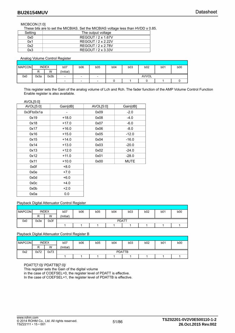
DatasheetDatasheet
51/86 TSZ02201-0V2V0E500110-1-2© 2014 ROHM Co., Ltd. All rights reserved.
26.Oct.2015 Rev.002
www.rohm.com
TSZ22111 • 15 • 001
BU26154MUV
MICBCON [1:0] These bits are to set the MICBIAS. Set the MICBIAS voltage less than HVDD x 0.85.
Setting The output voltage 0x0 REGOUT / 2 x 1.67V 0x1 REGOUT / 2 x 2.22V 0x2 REGOUT / 2 x 2.78V 0x3 REGOUT / 2 x 3.33V
Analog Volume Control Register
MAPCON b07 b06 b05 b04 b03 b02 b01 b00
R W (Initial)
0x0 0x3a 0x3b - - -
- - - 0 1 0 1 0
INDEX
AVVOL
This register sets the Gain of the analog volume of Lch and Rch. The fader function of the AMP Volume Control Function Enable register is also available. AVOL[5:0] AVOL[5:0] Gain[dB] AVOL[5:0] Gain[dB]
0x3Fto0x1a - 0x09 -2.0
0x19 +18.0 0x08 -4.0
0x18 +17.0 0x07 -6.0
0x17 +16.0 0x06 -8.0
0x16 +15.0 0x05 -12.0
0x15 +14.0 0x04 -16.0
0x14 +13.0 0x03 -20.0
0x13 +12.0 0x02 -24.0
0x12 +11.0 0x01 -28.0
0x11 +10.0 0x00 MUTE
0x0f +8.0
0x0e +7.0
0x0d +6.0
0x0c +4.0
0x0b +2.0
0x0a 0.0 Playback Digital Attenuator Control Register
MAPCON b07 b06 b05 b04 b03 b02 b01 b00
R W (Initial)
0x0 0x3e 0x3f
1 1 1 1 1 1 1 1
INDEX
PDATT
Playback Digital Attenuator Control Register B
MAPCON b07 b06 b05 b04 b03 b02 b01 b00
R W (Initial)
0x2 0x72 0x73
1 1 1 1 1 1 1 1
PDATTB
INDEX
PDATT[7:0]/ PDATTB[7:0]/ This register sets the Gain of the digital volume in the case of COEFSEL=0, the register level of PDATT is effective. In the case of COEFSEL=1, the register level of PDATTB is effective.
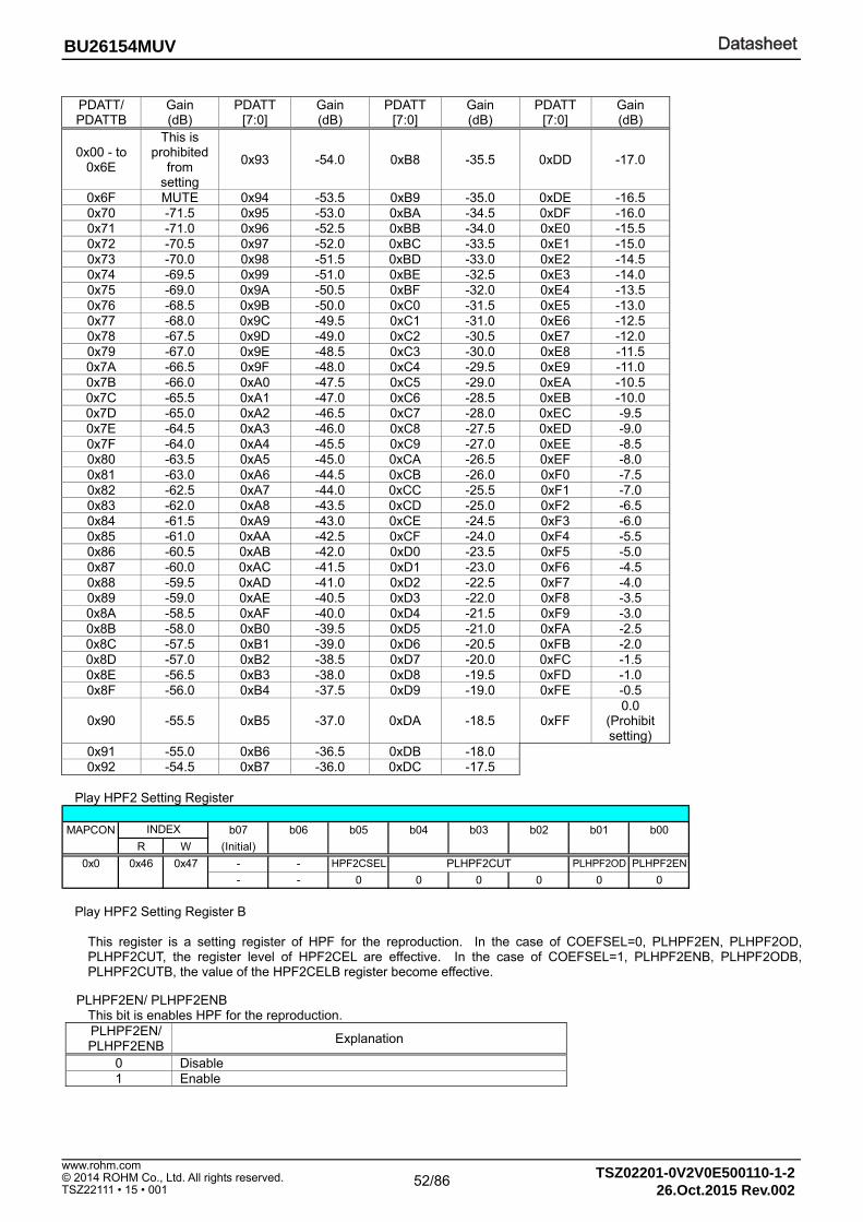
DatasheetDatasheet
52/86 TSZ02201-0V2V0E500110-1-2© 2014 ROHM Co., Ltd. All rights reserved.
26.Oct.2015 Rev.002
www.rohm.com
TSZ22111 • 15 • 001
BU26154MUV
PDATT/ PDATTB
Gain (dB)
PDATT [7:0]
Gain (dB)
PDATT [7:0]
Gain (dB)
PDATT [7:0]
Gain (dB)
0x00 - to 0x6E
This is prohibited
from setting
0x93 -54.0 0xB8 -35.5 0xDD -17.0
0x6F MUTE 0x94 -53.5 0xB9 -35.0 0xDE -16.5 0x70 -71.5 0x95 -53.0 0xBA -34.5 0xDF -16.0 0x71 -71.0 0x96 -52.5 0xBB -34.0 0xE0 -15.5 0x72 -70.5 0x97 -52.0 0xBC -33.5 0xE1 -15.0 0x73 -70.0 0x98 -51.5 0xBD -33.0 0xE2 -14.5 0x74 -69.5 0x99 -51.0 0xBE -32.5 0xE3 -14.0 0x75 -69.0 0x9A -50.5 0xBF -32.0 0xE4 -13.5 0x76 -68.5 0x9B -50.0 0xC0 -31.5 0xE5 -13.0 0x77 -68.0 0x9C -49.5 0xC1 -31.0 0xE6 -12.5 0x78 -67.5 0x9D -49.0 0xC2 -30.5 0xE7 -12.0 0x79 -67.0 0x9E -48.5 0xC3 -30.0 0xE8 -11.5 0x7A -66.5 0x9F -48.0 0xC4 -29.5 0xE9 -11.0 0x7B -66.0 0xA0 -47.5 0xC5 -29.0 0xEA -10.5 0x7C -65.5 0xA1 -47.0 0xC6 -28.5 0xEB -10.0 0x7D -65.0 0xA2 -46.5 0xC7 -28.0 0xEC -9.5 0x7E -64.5 0xA3 -46.0 0xC8 -27.5 0xED -9.0 0x7F -64.0 0xA4 -45.5 0xC9 -27.0 0xEE -8.5 0x80 -63.5 0xA5 -45.0 0xCA -26.5 0xEF -8.0 0x81 -63.0 0xA6 -44.5 0xCB -26.0 0xF0 -7.5 0x82 -62.5 0xA7 -44.0 0xCC -25.5 0xF1 -7.0 0x83 -62.0 0xA8 -43.5 0xCD -25.0 0xF2 -6.5 0x84 -61.5 0xA9 -43.0 0xCE -24.5 0xF3 -6.0 0x85 -61.0 0xAA -42.5 0xCF -24.0 0xF4 -5.5 0x86 -60.5 0xAB -42.0 0xD0 -23.5 0xF5 -5.0 0x87 -60.0 0xAC -41.5 0xD1 -23.0 0xF6 -4.5 0x88 -59.5 0xAD -41.0 0xD2 -22.5 0xF7 -4.0 0x89 -59.0 0xAE -40.5 0xD3 -22.0 0xF8 -3.5 0x8A -58.5 0xAF -40.0 0xD4 -21.5 0xF9 -3.0 0x8B -58.0 0xB0 -39.5 0xD5 -21.0 0xFA -2.5 0x8C -57.5 0xB1 -39.0 0xD6 -20.5 0xFB -2.0 0x8D -57.0 0xB2 -38.5 0xD7 -20.0 0xFC -1.5 0x8E -56.5 0xB3 -38.0 0xD8 -19.5 0xFD -1.0 0x8F -56.0 0xB4 -37.5 0xD9 -19.0 0xFE -0.5
0x90 -55.5 0xB5 -37.0 0xDA -18.5 0xFF 0.0
(Prohibit setting)
0x91 -55.0 0xB6 -36.5 0xDB -18.0 0x92 -54.5 0xB7 -36.0 0xDC -17.5
Play HPF2 Setting Register
MAPCON b07 b06 b05 b04 b03 b02 b01 b00
R W (Initial)
0x0 0x46 0x47 - - HPF2CSEL PLHPF2OD PLHPF2EN
- - 0 0 0 0 0 0
INDEX
PLHPF2CUT
Play HPF2 Setting Register B
This register is a setting register of HPF for the reproduction. In the case of COEFSEL=0, PLHPF2EN, PLHPF2OD, PLHPF2CUT, the register level of HPF2CEL are effective. In the case of COEFSEL=1, PLHPF2ENB, PLHPF2ODB, PLHPF2CUTB, the value of the HPF2CELB register become effective.
PLHPF2EN/ PLHPF2ENB
This bit is enables HPF for the reproduction. PLHPF2EN/ PLHPF2ENB
Explanation
0 Disable 1 Enable

DatasheetDatasheet
53/86 TSZ02201-0V2V0E500110-1-2© 2014 ROHM Co., Ltd. All rights reserved.
26.Oct.2015 Rev.002
www.rohm.com
TSZ22111 • 15 • 001
BU26154MUV
PLHPF2OD/ PLHPF2ODB This bit sets the degree of HPF for the reproduction.
PLHPF2OD/ PLHPF2ODB
Explanation
0 The second order 1 The first order
PLHPF2CUT/ PLHPF2CUTB This bit sets the cut-off frequency of HPF for reproduction. In the case of "0", HPF2CEL becomes effective for setting this bit.
PLHPF2CUT/ PLHPF2CUTB
Fs=8,16,32kHz
0x00 80Hz 0x01 100Hz 0x02 130Hz 0x03 160Hz 0x04 200Hz 0x05 260Hz 0x06 320Hz 0x07 400Hz
HPF2CEL/ HPF2CELB
I make HPF at the time of the reproduction programmable, or I make it parametric, or this bit sets it. HPF2CEL/ HPF2CELB
Explanation
0 PLHPF2CUT is effective. 1 PHPF2COEFL/H is effective.
Amplifier Volume Control Function Enable Register
MAPCON b07 b06 b05 b04 b03 b02 b01 b00
R W (Initial)
0x0 0x48 0x49 - - - - - - AVMUTE AVFADE
- - - - - - 0 0
INDEX
This register controls the fading function of the analog volume.
AVFADE
It sets the fading function of the analog volume to ON/OFF. AVFADE Explanation
0
Fading function OFF When a register set point of AVOL is just used for a real Volume price and wants to do it and changes a value, setting of the analog volume is updated immediately.
1
Fading function ON When a register set point of AVOL was updated, a gain of the analog volume changes by a +/-1 step towards a register set point after the update in step time for AVFCON register setting.
AVMUTE
When this is set, mute becomes effective for the analog volume at the time of reproduction. It can control fading for the mute shift by this bit by the analog volume forcibly by AVFADE. AVMUTE Explanation
0 As for the analog volume, a register set point of AVOL is effective.
1
At the time of re-start: The analog volume is set to MUTE. It comes back to the setting Volume in AVOL by canceling it because it writes it. This register level of AVOL cannot be replaced by the setting of this bit.

DatasheetDatasheet
54/86 TSZ02201-0V2V0E500110-1-2© 2014 ROHM Co., Ltd. All rights reserved.
26.Oct.2015 Rev.002
www.rohm.com
TSZ22111 • 15 • 001
BU26154MUV
Amplifier Volume Fader Control Register
MAPCON b07 b06 b05 b04 b03 b02 b01 b00
R W (Initial)
0x0 0x4a 0x4b - - - - -
- - - - - 0 0 0
INDEX
AVFCON
This register controls the amplifier volume fade function. AVFCON[2:0] These bits are to set the volume change step time of the amplifier volume fade function. The volume changes step by step with this setting period. Step time is in proportion to sampling frequency (fs) as following table.
AVFCON[2:0] fs conversion time(fs=48kHz)
0x0 1/fs 20.8µs 0x1 4/fs 83.3µs 0x2 16/fs 333µs 0x3 64/fs 1.33ms 0x4 256/fs 5.33ms 0x5 1024/fs 21.3ms 0x6 4096/fs 85.3ms 0x7 16384/fs 341.ms
Play Programmable HPF2 CoefL Register Play Programmable HPF2 CoefH Register
MAPCON b07 b06 b05 b04 b03 b02 b01 b00
R W (Initial)
0x0 0x4c 0x4d
0 0 0 0 0 0 0 0
0x0 0x4e 0x4f - -
0 0 0 0 0 0 0 0
PHPF2C0H
PHPF2C0L
INDEX
Play Programmable HPF2 CoefL Register B Play Programmable HPF2 CoefH Register B
MAPCON b07 b06 b05 b04 b03 b02 b01 b00
R W (Initial)
0x2 0x4c 0x4d
0 0 0 0 0 0 0 0
0x2 0x4e 0x4f - -
0 0 0 0 0 0 0 0
PHPF2C0LB
PHPF2C0HB
INDEX
It is the register settings of the programmable high path filter cut-off frequency for the reproduction. HPF2CSEL bit becomes effective when the register value is equal to "1". If COEFSEL=0, then the register level of PHPF2C0L, PHPF2C0H is effective. If COEFSEL=1, then the register level of PHPF2C0LB, PHPF2C0HB is effective. PHPF2C0L [7:0]/ PHPF2C0LB [7:0] PHPF2C0H [7:0]/ PHPF2C0HB [7:0] This sets the cut-off frequency of the programmable high path filter for the reproduction. Please refer for the setting method.

DatasheetDatasheet
55/86 TSZ02201-0V2V0E500110-1-2© 2014 ROHM Co., Ltd. All rights reserved.
26.Oct.2015 Rev.002
www.rohm.com
TSZ22111 • 15 • 001
BU26154MUV
DAC Clock Setting Register
MAPCON b07 b06 b05 b04 b03 b02 b01 b00
R W (Initial)
0x0 0x58 0x59 - - - - - -
- - 0 0 - - - -
INDEX
OSRSEL
This register sets the DAC clock movement to be used in this LSI.
OSRSEL [1:0] This register decides sampling frequency.
Setting Explanation 0x0 8k,11.025k,12kHz 0x1 16k,22.05k,24kHz 0x2 32k,44.1k,48kHz 0x3 This is prohibited from setting
Mic Interface Control Register
MAPCON b07 b06 b05 b04 b03 b02 b01 b00
R W (Initial)
0x0 0x5a 0x5b - - - MINDIF -
1 0 0 - - - 0 -
INDEX
MINVOL
This register controls the microphone input interface.
MINDIF
It sets the MIC movement mode. Setting Explanation
0 Single-end mode 1 Differential mode
MINVOL
This bit sets the Analog MIC volume. MINVOL Gain 0x00 6dB 0x01 9dB 0x02 12dB 0x03 15dB 0x04 18dB 0x05 21dB 0x06 24dB 0x07 27dB
Sound Effect Mode Register
MAPCON b07 b06 b05 b04 b03 b02 b01 b00
R W (Initial)
0x0 0x5c 0x5d SEMODE[7] - - - -
0 - - - - 0 0 0
INDEX
SEMODE[2:0]
Sound Effect Mode Register B
MAPCON b07 b06 b05 b04 b03 b02 b01 b00
R W (Initial)
0x2 0x5c 0x5d SEMODEB[7] - - - -
0 - - - - 0 0 0
INDEX
SEMODEB[2:0]
If COEFSEL=0, then the register level of SEMODE is effective. If COEFSEL=1, then the value of the SEMODEB register becomes effective.

DatasheetDatasheet
56/86 TSZ02201-0V2V0E500110-1-2© 2014 ROHM Co., Ltd. All rights reserved.
26.Oct.2015 Rev.002
www.rohm.com
TSZ22111 • 15 • 001
BU26154MUV
SEMODE [7]/SEMODEB [7] You choose a course putting Filter Block, and please refer to the clause of "the signal flow" of "the function explanation" for Filter Block.
SEMODE[7]/ SEMODEB [7]
Explanation
0 Use Filter Block on Recording path. 1 Use Filter Block on Playback path.
SEMODE [2:0]/ SEMODEB [2:0]
This sets distribution of EQ/Notch Filter. SEMODE[2:0]/ SEMODEB[2:0]
Explanation
0x0 Notch5 band / EQ0 band 0x1 Notch4 band / EQ1 band 0x2 Notch3 band / EQ2 band 0x3 Notch2 band / EQ3 band 0x4 Notch1 band / EQ4 band 0x5 Notch0 band / EQ5 band
When "0x01" is set, Band0 to Band3 filters Notch, and Band4 becomes the EQ.
SAI Transmitter Control Register
MAPCON b07 b06 b05 b04 b03 b02 b01 b00
R W (Initial)
0x0 0x60 0x61 FMTO MSBO ISSCKO AFOO DLYO WSLO
1 1 0 0 0 0 0 0
PCMFO24
INDEX
This register controls the SAI transmission format setting. The RECPLAY bit of the Record/Playback Running Control register, please change this register in recording stop state (0x0), and please use it by setting again same as the SAI reception side (SAI Receiver Control register).
WSLO
You appoint LRCLK polarity at the time of the transmission of this LSI, and please set this bit in "1" in (FMTO at the time of "1") in a transfer mode by all means in the frame same period.
Setting Explanation
0 Left channel transmission at SAI_LRCLK is “L” level; right channel transmission at SAI_LRCLK is “H” level.
1 Left channel transmission at SAI_LRCLK is “H” level; right channel transmission at SAI_LRCLK is “L” level.l
DLYO
This bit appoints 1 clock delay existence / nothing of transmission data. Setting Explanation
0 Serial data delay existence 1 Serial data delay nothing
AFOO
You appoint in front of filling / attacking the enemy from behind of transmission data, and, in the case of a slave mode, this bit is ignored, and it is in previous final stage is fixed, and please set this bit in "0" in (FMTO at the time of "1") in a transfer mode by all means in the frame same period.
Setting Explanation 0 Left-justify 1 Right-justify
ISSCKO
This bit sets BCLK terminal to 32fs/64fs. Setting Explanation
0 32fs 1 64fs
MSBO
This bit sets the MSB first /LSB first data transmission. Setting Explanation
0 MSB first 1 LSB first

DatasheetDatasheet
57/86 TSZ02201-0V2V0E500110-1-2© 2014 ROHM Co., Ltd. All rights reserved.
26.Oct.2015 Rev.002
www.rohm.com
TSZ22111 • 15 • 001
BU26154MUV
FMTO This bit sets the transmission mode.
Setting Explanation 0 LRCLK transfer mode 1 Frame synchronization transfer mode
PCMFO24
This bit sets PCM format of the SAI transmission. Setting Explanation
0x2 16bit PCM 0x3 24bit PCM
Other than the above
This is prohibited from setting
SAI Receiver Control Register
MAPCON b07 b06 b05 b04 b03 b02 b01 b00
R W (Initial)
0x0 0x62 0x63 FMTI MSBI ISSCKI AFOI DLYI WSLI
1 1 0 0 0 0 0 0
INDEX
PCMFI24
This register is a register controlling SAI reception format setting, and RECPLAY bit of the Record/Playback Running Control register, please change this register in recording stop state (0x0), and please use it by setting again same as the SAI transmission side (SAI Transmitter Control register).
WSLI This bit selects LRCLK polarity of the LSI. This bit must be set to “1” when at Flame synchronous transfer mode (FMTI is “1”).
Setting Explanation
0 Left channel is received when SAI_LRCLK is “L” level, right channel is received at SAI_LRCLK is “H” level.
1 Left channel is received when SAI_LRCLK is “H” level, right channel is received at SAI_LRCLK is “L” level.
DLYI This bit specifies the existence for serial input data one clock delay of master device.
Setting Explanation 0 Serial data delay existence 1 Serial data delay nothing
AFOI This bit sets the receiving data to be Left-justify or Right-justify. This bit must be set to “0” when at Flame synchronous
transfer mode (FMTI is “1”). Setting Explanation
0 Left-justify 1 Right-justify
ISSCKI
This bit sets the sampling frequency of SAI_BCLK pin. Setting Explanation
0 32fs 1 64fs
MSBI
This bit sets the SAI receiving data to be MSB-first or LSB-first. Setting Explanation
0 MSB first 1 LSB first
FMTI
This bit sets the receiving mode Setting Explanation
0 LRCLK transfer mode 1 Frame synchronization transfer mode

DatasheetDatasheet
58/86 TSZ02201-0V2V0E500110-1-2© 2014 ROHM Co., Ltd. All rights reserved.
26.Oct.2015 Rev.002
www.rohm.com
TSZ22111 • 15 • 001
BU26154MUV
PCMFI24 This bit sets the SAI PCM receiving format.
Setting Explanation 0x2 16bit PCM 0x3 24bit PCM
Other than the above
This is prohibited from setting
SAI Mode select Register
MAPCON b07 b06 b05 b04 b03 b02 b01 b00
R W (Initial)
0x0 0x64 0x65 - - - BSWP - - - MST
- - - 0 - - - 0
INDEX
This register is a register setting a movement mode of SAI, and RECPLAY bit of the Record/Playback Running Control register, please change this register in recording stop state (0x0).
MST It appoints whether this bit uses SAI with a master mode or a slave mode.
Setting Explanation 0 Slave mode 1 Master mode
BSWP
As for this bit, it is done byte swap I2S data with PCM format by 16bitPCM without depending on the setting of the I2S Receiver Control/I2S Transmitter Control register at the time of setting when I set byte swap having I2S or not on the same side of transmission and reception data and there is byte swap and sets it.
Setting Explanation
0 There is no byte swap (16bit data line up :15bit-8bit,7bit-0bit) (24bit data line up :23bit-16bit,15bit-8bit,7bit-0bit)
1 There is byte swap (16bit data line up :7bit-0bit,15bit-8bit) (24bit data line up :7bit-0bit,15bit-8bit 23bit-16bit)
DSP Filter Function Enable Register
MAPCON b07 b06 b05 b04 b03 b02 b01 b00
R W (Initial)
0x0 0x66 0x67 HPF2OD EQ4EN EQ3EN EQ2EN EQ1EN EQ0EN HPF2EN HPF1EN
0 0 0 0 0 0 0 1
INDEX
DSP Filter Function Enable Register
MAPCON b07 b06 b05 b04 b03 b02 b01 b00
R W (Initial)
0x0 0x66 0x67 HPF2OD EQ4EN EQ3EN EQ2EN EQ1EN EQ0EN HPF2EN HPF1EN
0 0 0 0 0 0 0 1
INDEX
DSP Filter Function Enable Register B
MAPCON b07 b06 b05 b04 b03 b02 b01 b00
R W (Initial)
0x2 0x66 0x67 HPF2ODB EQ4ENB EQ3ENB EQ2ENB EQ1ENB EQ0ENB HPF2ENB HPF1ENB
0 0 0 0 0 0 0 1
INDEX
This register sets the filter function of the digital code processing ON/OFF. If COEFSEL=0, then register level of HPF1/2EN, EQ0/1/2/3/4EN, HPF2OD is effective. If COEFSEL=1, then value of HPF1/2ENB, EQ0/1/2/3/4ENB, HPF2ODB register becomes effective.

DatasheetDatasheet
59/86 TSZ02201-0V2V0E500110-1-2© 2014 ROHM Co., Ltd. All rights reserved.
26.Oct.2015 Rev.002
www.rohm.com
TSZ22111 • 15 • 001
BU26154MUV
HPF1EN/ HPF1ENB This bit is to set ON or OFF of a first-order high pass filter for DC cut. Do not change this bit during operation of the recording (0x13/0x14: RECPLAY=0x1, 0x3, or 0x7). If this bit is changed, the noise may be generated. When this IC being operated the playing (RECPLAY=0x2), this bit operating don't have effective. HPF1EN/ HPF1ENB
Explanation
0 Primary high-pass filter OFF for the DC cut 1 Primary high-pass filter ON for the DC cut
HPF2EN/ HPF2ENB
This bit is to set ON or OFF of a second-order high pass filter for noise cut. Do not change this bit during operation of the recording (RECPLAY=0x1,0x3, or 0x7). If this bit is changed, the noise may be generated. The bit of HPF2EN is effective only when 0xA6/0xA7:RLPFEN is enable. HPF2EN/ HPF2ENB
Explanation
0 Second high-pass filter OFF for noise reduction 1 Second high-pass filter ON for noise reduction
EQ0EN/EQ0ENB
This bit is to set ON or OFF of equalizer band 0. In case of changing this bit during recording and playback operation (RECPLAY=0x1, 0x2, 0x3, or 0x7), enables digital volume fade function (0x68/0x69: DVFADE=1) and then change the gain to 0dB. EQ0EN/ EQ0ENB
Explanation
0 Equalizer band 0 OFF 1 Equalizer band 0 ON
EQ1EN/EQ1ENB
This bit is to set ON or OFF of equalizer band 1. In case of changing this bit during recording and playback operation (0x13/0x14: RECPLAY=0x1, 0x2, 0x3, or 0x7), enables digital volume fade function (0x68/0x69: DVFADE=1) and then change the gain to 0dB. EQ1EN/ EQ1ENB
Explanation
0 Equalizer band 1 OFF 1 Equalizer band 1 ON
EQ2EN/EQ2ENB
This bit is to set ON or OFF of equalizer band 2. In case of changing this bit during recording and playback operation (0x13/0x14: RECPLAY=0x1, 0x2, 0x3, or 0x7), enables digital volume fade function (0x68/0x69: DVFADE=1) and then change the gain to 0dB. EQ2EN/ EQ2ENB
Explanation
0 Equalizer band 2 OFF 1 Equalizer band 2 ON
EQ3EN/EQ3ENB
This bit is to set ON or OFF of equalizer band 3. In case of changing this bit during recording and playback operation (0x13/0x14: RECPLAY=0x1, 0x2, 0x3, or 0x7), enables digital volume fade function (0x68/0x69: DVFADE=1) and then change the gain to 0dB. EQ3EN/ EQ3ENB
Explanation
0 Equalizer band 3 OFF 1 Equalizer band 3 ON
EQ4EN/EQ4ENB
This bit is to set ON or OFF of equalizer band 4. In case of changing this bit during recording and playback operation (0x13/0x14: RECPLAY=0x1, 0x2, 0x3, or 0x7), enables digital volume fade function (0x68/0x69: DVFADE=1) and then change the gain to 0dB. EQ4EN/ EQ4ENB
Explanation
0 Equalizer band 4 OFF 1 Equalizer band 4 ON

DatasheetDatasheet
60/86 TSZ02201-0V2V0E500110-1-2© 2014 ROHM Co., Ltd. All rights reserved.
26.Oct.2015 Rev.002
www.rohm.com
TSZ22111 • 15 • 001
BU26154MUV
HPF2OD/HPFODB This bit is to set number of high pass filter order (HPF2EN bit) for noise cut. In recording or playback operation(0x13/0x14: RECPLAY≠0),do not change this bit. If this bit is changed, the noise may be generated. HPF2OD/ HPF2ODB
Explanation
0 The second filter 1 Primary filter
Digital Volume Control Function Enable Register
MAPCON b07 b06 b05 b04 b03 b02 b01 b00
R W (Initial)
0x0 0x68 0x69 - - - DVMUTE DVFADE - RALCEN PALCEN
- - - 0 0 - 0 0
INDEX
This register sets ON/OFF of digital, the Volume control function.
PALCEN This bit is to set ON or OFF of the playing ALC. It must not be wrote during recording and playback operation (0x13/0x14: RECPLAY=0x1, 0x3, or 0x7). If this bit was set as the operation, this IC cannot guarantee correct operating. PALCEN Explanation
0 Reproduction ALC OFF 1 Reproduction ALCON
RALCEN
This bit is to set ON or OFF of the recording ALC. It must not be wrote during recording and playback operation (0x13/0x14: RECPLAY=0x2). If this bit was set as the operation, this IC cannot guarantee correct operating. RALCEN Explanation
0 Recording ALC OFF 1 Recording ALC ON
DVFADE
This bit is to set ON or OFF of the digital volume fade function. The fade function is effective for recording/playback digital volume and equalizer gain. DVFADE Explanation
0
Fading Function OFF: The register setting value of RDATT, PDATT and EQGAIN0 to 3 is used actual volume value as it is. Therefore the value is effective immediate.
1
Fading Function ON: The volume is changing to the register setting value of RDATT, PDATT and EQGAIN0 to 3 with 1 step per DVFCON register step time.
DVMUTE
This bit is to set MUTE of the digital volume. This mute function is effective for the recording digital volume at recording and effective for playback digital volume at playback. The fade function by DVFADE is effective against the volume change by this bit. DVMUTE Explanation
0 Register value of RDVOL and PDATT is effective.
1
Digital volume is set to MUTE. Register value of RDVOL and PDATT cannot be changed by this bit, the volume is resumed by releasing this bit (DVMUTE=0) to the original setting value of RDVOL and PDVOL.

DatasheetDatasheet
61/86 TSZ02201-0V2V0E500110-1-2© 2014 ROHM Co., Ltd. All rights reserved.
26.Oct.2015 Rev.002
www.rohm.com
TSZ22111 • 15 • 001
BU26154MUV
Mixer & Volume Control Register
MAPCON b07 b06 b05 b04 b03 b02 b01 b00
R W (Initial)
0x0 0x6a 0x6b
0 0 0 0 0 0 0 0
RMCON LMCON
INDEX
DVFCON
This register controls L/R mixer processing at the time of the SAI reception and a fading function of the digital Volume.
LMCON[1:0] This bit sets the input channel of SAI reception data of the DAC (Lch).
Setting Explanation 0x0 I use L 0x1 I use R 0x2 I use (L+R) 0x3 I use (L+R)/2
RMCON[1:0]
This bit sets it about SAI reception data which channel you input into DAC (Rch). Setting Explanation
0x0 I use R 0x1 I use L 0x2 I use (L+R) 0x3 I use (L+R)/2
DVFCON[3:0]
These bits are to set the volume change step time of the digital volume fade function. The volume changes step by step (0.5dB) with this setting period. Step time is in proportion to sampling frequency (fs) as following table. Setting fs conversion Time(fs=48kHz)
0x0 1/fs 20.8µs 0x1 2/fs 41.7µs 0x2 4/fs 83.3µs 0x3 8/fs 167µs 0x4 16/fs 333µs 0x5 32/fs 667µs 0x6 64/fs 1.33ms 0x7 128/fs 2.67ms 0x8 256/fs 5.33ms 0x9 512/fs 10.7ms 0xA 1024/fs 21.3ms 0xB 2048/fs 42.7ms 0xC 4096/fs 85.3ms 0xD 8192/fs 171ms 0xE 16384/fs 341ms
Record Digital Attenuator Control Register
MAPCON b07 b06 b05 b04 b03 b02 b01 b00
R W (Initial)
0x0 0x6c 0x6d
1 1 1 1 1 1 1 1
INDEX
RDVOL
This register sets digital Volume Gain of the recording course. MUTE could be set from -71.5dB to 0.0dB by 0.5dB step.

DatasheetDatasheet
62/86 TSZ02201-0V2V0E500110-1-2© 2014 ROHM Co., Ltd. All rights reserved.
26.Oct.2015 Rev.002
www.rohm.com
TSZ22111 • 15 • 001
BU26154MUV
RDATT[7:0] Setting Gain(dB) Setting Gain(dB) Setting Gain(dB) Setting Gain(dB)
0x00 - 0x6E
This is prohibited
from setting
0x93 -54.0 0xB8 -35.5 0xDD -17.0
0x6F MUTE 0x94 -53.5 0xB9 -35.0 0xDE -16.5 0x70 -71.5 0x95 -53.0 0xBA -34.5 0xDF -16.0 0x71 -71.0 0x96 -52.5 0xBB -34.0 0xE0 -15.5 0x72 -70.5 0x97 -52.0 0xBC -33.5 0xE1 -15.0 0x73 -70.0 0x98 -51.5 0xBD -33.0 0xE2 -14.5 0x74 -69.5 0x99 -51.0 0xBE -32.5 0xE3 -14.0 0x75 -69.0 0x9A -50.5 0xBF -32.0 0xE4 -13.5 0x76 -68.5 0x9B -50.0 0xC0 -31.5 0xE5 -13.0 0x77 -68.0 0x9C -49.5 0xC1 -31.0 0xE6 -12.5 0x78 -67.5 0x9D -49.0 0xC2 -30.5 0xE7 -12.0 0x79 -67.0 0x9E -48.5 0xC3 -30.0 0xE8 -11.5 0x7A -66.5 0x9F -48.0 0xC4 -29.5 0xE9 -11.0 0x7B -66.0 0xA0 -47.5 0xC5 -29.0 0xEA -10.5 0x7C -65.5 0xA1 -47.0 0xC6 -28.5 0xEB -10.0 0x7D -65.0 0xA2 -46.5 0xC7 -28.0 0xEC -9.5 0x7E -64.5 0xA3 -46.0 0xC8 -27.5 0xED -9.0 0x7F -64.0 0xA4 -45.5 0xC9 -27.0 0xEE -8.5 0x80 -63.5 0xA5 -45.0 0xCA -26.5 0xEF -8.0 0x81 -63.0 0xA6 -44.5 0xCB -26.0 0xF0 -7.5 0x82 -62.5 0xA7 -44.0 0xCC -25.5 0xF1 -7.0 0x83 -62.0 0xA8 -43.5 0xCD -25.0 0xF2 -6.5 0x84 -61.5 0xA9 -43.0 0xCE -24.5 0xF3 -6.0 0x85 -61.0 0xAA -42.5 0xCF -24.0 0xF4 -5.5 0x86 -60.5 0xAB -42.0 0xD0 -23.5 0xF5 -5.0 0x87 -60.0 0xAC -41.5 0xD1 -23.0 0xF6 -4.5 0x88 -59.5 0xAD -41.0 0xD2 -22.5 0xF7 -4.0 0x89 -59.0 0xAE -40.5 0xD3 -22.0 0xF8 -3.5 0x8A -58.5 0xAF -40.0 0xD4 -21.5 0xF9 -3.0 0x8B -58.0 0xB0 -39.5 0xD5 -21.0 0xFA -2.5 0x8C -57.5 0xB1 -39.0 0xD6 -20.5 0xFB -2.0 0x8D -57.0 0xB2 -38.5 0xD7 -20.0 0xFC -1.5 0x8E -56.5 0xB3 -38.0 0xD8 -19.5 0xFD -1.0 0x8F -56.0 0xB4 -37.5 0xD9 -19.0 0xFE -0.5 0x90 -55.5 0xB5 -37.0 0xDA -18.5 0xFF 0.0 0x91 -55.0 0xB6 -36.5 0xDB -18.0 0x92 -54.5 0xB7 -36.0 0xDC -17.5
Playback Effect Volume Control Register
MAPCON b07 b06 b05 b04 b03 b02 b01 b00
R W (Initial)
0x0 0x70 0x71
1 1 1 1 1 1 1 1
INDEX
Effect VOL
Playback Effect Volume Control Register B
MAPCON b07 b06 b05 b04 b03 b02 b01 b00
R W (Initial)
0x2 0x70 0x71
1 1 1 1 1 1 1 1
Effect VOLB
INDEX
This register sets the digital Volume Gain of the reproduction course. If COEFSEL=0, then register level of Effect Vol is effective. If COEFSEL=1, then value of the Effect Vol B register becomes effective. MUTE could be set from -71.5dB to 0.0dB by 0.5dB step.

DatasheetDatasheet
63/86 TSZ02201-0V2V0E500110-1-2© 2014 ROHM Co., Ltd. All rights reserved.
26.Oct.2015 Rev.002
www.rohm.com
TSZ22111 • 15 • 001
BU26154MUV
Effect Vol[7:0]/ Effect Vol B[7:0 Sets the Digital Volume Gain.
Effect Vol/ Effect Vol B
Gain(dB) Setting Gain(dB) Setting Gain(dB) Setting Gain(dB)
0x00 - 0x6E
This is prohibited
from setting
0x93 -54.0 0xB8 -35.5 0xDD -17.0
0x6F MUTE 0x94 -53.5 0xB9 -35.0 0xDE -16.5 0x70 -71.5 0x95 -53.0 0xBA -34.5 0xDF -16.0 0x71 -71.0 0x96 -52.5 0xBB -34.0 0xE0 -15.5 0x72 -70.5 0x97 -52.0 0xBC -33.5 0xE1 -15.0 0x73 -70.0 0x98 -51.5 0xBD -33.0 0xE2 -14.5 0x74 -69.5 0x99 -51.0 0xBE -32.5 0xE3 -14.0 0x75 -69.0 0x9A -50.5 0xBF -32.0 0xE4 -13.5 0x76 -68.5 0x9B -50.0 0xC0 -31.5 0xE5 -13.0 0x77 -68.0 0x9C -49.5 0xC1 -31.0 0xE6 -12.5 0x78 -67.5 0x9D -49.0 0xC2 -30.5 0xE7 -12.0 0x79 -67.0 0x9E -48.5 0xC3 -30.0 0xE8 -11.5 0x7A -66.5 0x9F -48.0 0xC4 -29.5 0xE9 -11.0 0x7B -66.0 0xA0 -47.5 0xC5 -29.0 0xEA -10.5 0x7C -65.5 0xA1 -47.0 0xC6 -28.5 0xEB -10.0 0x7D -65.0 0xA2 -46.5 0xC7 -28.0 0xEC -9.5 0x7E -64.5 0xA3 -46.0 0xC8 -27.5 0xED -9.0 0x7F -64.0 0xA4 -45.5 0xC9 -27.0 0xEE -8.5 0x80 -63.5 0xA5 -45.0 0xCA -26.5 0xEF -8.0 0x81 -63.0 0xA6 -44.5 0xCB -26.0 0xF0 -7.5 0x82 -62.5 0xA7 -44.0 0xCC -25.5 0xF1 -7.0 0x83 -62.0 0xA8 -43.5 0xCD -25.0 0xF2 -6.5 0x84 -61.5 0xA9 -43.0 0xCE -24.5 0xF3 -6.0 0x85 -61.0 0xAA -42.5 0xCF -24.0 0xF4 -5.5 0x86 -60.5 0xAB -42.0 0xD0 -23.5 0xF5 -5.0 0x87 -60.0 0xAC -41.5 0xD1 -23.0 0xF6 -4.5 0x88 -59.5 0xAD -41.0 0xD2 -22.5 0xF7 -4.0 0x89 -59.0 0xAE -40.5 0xD3 -22.0 0xF8 -3.5 0x8A -58.5 0xAF -40.0 0xD4 -21.5 0xF9 -3.0 0x8B -58.0 0xB0 -39.5 0xD5 -21.0 0xFA -2.5 0x8C -57.5 0xB1 -39.0 0xD6 -20.5 0xFB -2.0 0x8D -57.0 0xB2 -38.5 0xD7 -20.0 0xFC -1.5 0x8E -56.5 0xB3 -38.0 0xD8 -19.5 0xFD -1.0 0x8F -56.0 0xB4 -37.5 0xD9 -19.0 0xFE -0.5 0x90 -55.5 0xB5 -37.0 0xDA -18.5 0xFF 0.0 0x91 -55.0 0xB6 -36.5 0xDB -18.0 0x92 -54.5 0xB7 -36.0 0xDC -17.5

DatasheetDatasheet
64/86 TSZ02201-0V2V0E500110-1-2© 2014 ROHM Co., Ltd. All rights reserved.
26.Oct.2015 Rev.002
www.rohm.com
TSZ22111 • 15 • 001
BU26154MUV
EQ Band0 Gain Setting Register EQ Band1 Gain Setting Register EQ Band2 Gain Setting Register EQ Band3 Gain Setting Register EQ Band4 Gain Setting Register
MAPCON b07 b06 b05 b04 b03 b02 b01 b00
R W (Initial)
0x0 0x74 0x75
1 1 1 0 0 1 1 1
0x0 0x76 0x77
1 1 1 0 0 1 1 1
0x0 0x78 0x79
1 1 1 0 0 1 1 1
0x0 0x7a 0x7b
1 1 1 0 0 1 1 1
0x0 0x7c 0x7d
1 1 1 0 0 1 1 1
EQGAIN4
EQGAIN3
EQGAIN2
EQGAIN1
INDEX
EQGAIN0
EQ Band0 Gain Setting Register B EQ Band1 Gain Setting Register B EQ Band2 Gain Setting Register B EQ Band3 Gain Setting Register B EQ Band4 Gain Setting Register B
MAPCON b07 b06 b05 b04 b03 b02 b01 b00
R W (Initial)
0x2 0x74 0x75
1 1 1 0 0 1 1 1
0x2 0x76 0x77
1 1 1 0 0 1 1 1
0x2 0x78 0x79
1 1 1 0 0 1 1 1
0x2 0x7a 0x7b
1 1 1 0 0 1 1 1
0x2 0x7c 0x7d
1 1 1 0 0 1 1 1
EQGAIN0B
EQGAIN1B
INDEX
EQGAIN2B
EQGAIN3B
EQGAIN4B
This register sets the gain of each band of the equalizer. If COEFSEL=0, then the register level of EQGAIN0 to 4 is effective. If COEFSEL=1, then value of the EQGAIN0B to EQGAIN4B register becomes effective. This register can set EQ gain from -71.5dB to 12.0dB(step by step 0.5dB). Also it can set MUTE. EQ can work as a notch filter by MUTE setting. EQGAIN/ EQGAINB
0 - to 4 [7:0]
Gain (0dB)
EQGAIN/ EQGAINB 0 - to4[7:0]
Gain (0dB)
EQGAIN/EQGAINB0 - to4[7:0]
Gain (dB)
EQGAIN/EQGAINB0 - to4[7:0]
Gain (dB)
0x00 - to 0x57 MUTE 0x82 -50.5 0xAD -29.0 0xD8 -7.5 0x58 -71.5 0x83 -50.0 0xAE -28.5 0xD9 -7.0 0x59 -71.0 0x84 -49.5 0xAF -28.0 0xDA -6.5 0x5A -70.5 0x85 -49.0 0xB0 -27.5 0xDB -6.0 0x5B -70.0 0x86 -48.5 0xB1 -27.0 0xDC -5.5 0x5C -69.5 0x87 -48.0 0xB2 -26.5 0xDD -5.0 0x5D -69.0 0x88 -47.5 0xB3 -26.0 0xDE -4.5 0x5E -68.5 0x89 -47.0 0xB4 -25.5 0xDF -4.0 0x5F -68.0 0x8A -46.5 0xB5 -25.0 0xE0 -3.5 0x60 -67.5 0x8B -46.0 0xB6 -24.5 0xE1 -3.0 0x61 -67.0 0x8C -45.5 0xB7 -24.0 0xE2 -2.5 0x62 -66.5 0x8D -45.0 0xB8 -23.5 0xE3 -2.0 0x63 -66.0 0x8E -44.5 0xB9 -23.0 0xE4 -1.5 0x64 -65.5 0x8F -44.0 0xBA -22.5 0xE5 -1.0 0x65 -65.0 0x90 -43.5 0xBB -22.0 0xE6 -0.5 0x66 -64.5 0x91 -43.0 0xBC -21.5 0xE7 0.0 0x67 -64.0 0x92 -42.5 0xBD -21.0 0xE8 0.5 0x68 -63.5 0x93 -42.0 0xBE -20.5 0xE9 1.0 0x69 -63.0 0x94 -41.5 0xBF -20.0 0xEA 1.5 0x6A -62.5 0x95 -41.0 0xC0 -19.5 0xEB 2.0

DatasheetDatasheet
65/86 TSZ02201-0V2V0E500110-1-2© 2014 ROHM Co., Ltd. All rights reserved.
26.Oct.2015 Rev.002
www.rohm.com
TSZ22111 • 15 • 001
BU26154MUV
0x6B -62.0 0x96 -40.5 0xC1 -19.0 0xEC 2.5 0x6C -61.5 0x97 -40.0 0xC2 -18.5 0xED 3.0 0x6D -61.0 0x98 -39.5 0xC3 -18.0 0xEE 3.5 0x6E -60.5 0x99 -39.0 0xC4 -17.5 0xEF 4.0 0x6F -60.0 0x9A -38.5 0xC5 -17.0 0xF0 4.5 0x70 -59.5 0x9B -38.0 0xC6 -16.5 0xF1 5.0 0x71 -59.0 0x9C -37.5 0xC7 -16.0 0xF2 5.5 0x72 -58.5 0x9D -37.0 0xC8 -15.5 0xF3 6.0 0x73 -58.0 0x9E -36.5 0xC9 -15.0 0xF4 6.5 0x74 -57.5 0x9F -36.0 0xCA -14.5 0xF5 7.0 0x75 -57.0 0xA0 -35.5 0xCB -14.0 0xF6 7.5 0x76 -56.5 0xA1 -35.0 0xCC -13.5 0xF7 8.0 0x77 -56.0 0xA2 -34.5 0xCD -13.0 0xF8 8.5 0x78 -55.5 0xA3 -34.0 0xCE -12.5 0xF9 9.0 0x79 -55.0 0xA4 -33.5 0xCF -12.0 0xFA 9.5 0x7A -54.5 0xA5 -33.0 0xD0 -11.5 0xFB 10.0 0x7B -54.0 0xA6 -32.5 0xD1 -11.0 0xFC 10.5 0x7C -53.5 0xA7 -32.0 0xD2 -10.5 0xFD 11.0 0x7D -53.0 0xA8 -31.5 0xD3 -10.0 0xFE 11.5 0x7E -52.5 0xA9 -31.0 0xD4 -9.5 0xFF 12.0 0x7F -52.0 0xAA -30.5 0xD5 -9.0 0x80 -51.5 0xAB -30.0 0xD6 -8.5 0x81 -51.0 0xAC -29.5 0xD7 -8.0
High Pass Filter2 Cut-off Control Register
MAPCON b07 b06 b05 b04 b03 b02 b01 b00
R W (Initial)
0x0 0x7e 0x7f - - - - -
- - - - - 0 0 0
INDEX
HPF2CUT
This register is to set the cut-off frequency of the high-pass filter for the noise reduction during recording. Don’t change the setting of this register under the filter processing concerned(HPF2EN="1" and RELPLAY=0x1,0x3 or 0x7).
HPF2CUT[2:0] These set the cut-off frequency of the noise reduction high-pass filter during recording and the numerical value of below list expresses 1.5dB damping and 3dB damping frequency in each second order filter(HPF2OD="1") and one order filter (HPF2OD="0").
HPF2CUT [2:0]
Cut-off Frequency(Hz) fs=8kHz, 16kHz, 32kHz
fs=11.025kHz, 22.05kHz, 44.1kHz
fs=12kHz, 24kHz, 48kHz
0x0 80 110 120 0x1 100 138 150 0x2 130 179 195 0x3 160 221 240 0x4 200 276 300 0x5 260 358 390 0x6 320 441 480 0x7 400 551 600

DatasheetDatasheet
66/86 TSZ02201-0V2V0E500110-1-2© 2014 ROHM Co., Ltd. All rights reserved.
26.Oct.2015 Rev.002
www.rohm.com
TSZ22111 • 15 • 001
BU26154MUV
Programmable Equalizer Band0 Coefficient-a0 (L) Register Programmable Equalizer Band0 Coefficient-a0 (H) Register Programmable Equalizer Band0 Coefficient-a1 (L) Register Programmable Equalizer Band0 Coefficient-a1 (H) Register Programmable Equalizer Band1 Coefficient-a0 (L) Register Programmable Equalizer Band1 Coefficient-a0 (H) Register Programmable Equalizer Band1 Coefficient-a1 (L) Register Programmable Equalizer Band1 Coefficient-a1 (H) Register Programmable Equalizer Band2 Coefficient-a0 (L) Register Programmable Equalizer Band2 Coefficient-a0 (H) Register Programmable Equalizer Band2 Coefficient-a1 (L) Register Programmable Equalizer Band2 Coefficient-a1 (H) Register Programmable Equalizer Band3 Coefficient-a0 (L) Register Programmable Equalizer Band3 Coefficient-a0 (H) Register Programmable Equalizer Band3 Coefficient-a1 (L) Register Programmable Equalizer Band3 Coefficient-a1 (H) Register Programmable Equalizer Band4 Coefficient-a0 (L) Register Programmable Equalizer Band4 Coefficient-a0 (H) Register Programmable Equalizer Band4 Coefficient-a1 (L) Register Programmable Equalizer Band4 Coefficient-a1 (H) Register
MAPCON b07 b06 b05 b04 b03 b02 b01 b00
R W (Initial)
0x0 0x80 0x81
0 0 0 0 0 0 0 0
0x0 0x82 0x83
0 0 0 0 0 0 0 0
0x0 0x84 0x85
0 0 0 0 0 0 0 0
0x0 0x86 0x87
0 0 0 0 0 0 0 0
0x0 0x88 0x89
0 0 0 0 0 0 0 0
0x0 0x8a 0x8b
0 0 0 0 0 0 0 0
0x0 0x8c 0x8d
0 0 0 0 0 0 0 0
0x0 0x8e 0x8f
0 0 0 0 0 0 0 0
0x0 0x90 0x91
0 0 0 0 0 0 0 0
0x0 0x92 0x93
0 0 0 0 0 0 0 0
0x0 0x94 0x95
0 0 0 0 0 0 0 0
0x0 0x96 0x97
0 0 0 0 0 0 0 0
0x0 0x98 0x99
0 0 0 0 0 0 0 0
0x0 0x9a 0x9b
0 0 0 0 0 0 0 0
0x0 0x9c 0x9d
0 0 0 0 0 0 0 0
0x0 0x9e 0x9f
0 0 0 0 0 0 0 0
0x0 0xa0 0xa1
0 0 0 0 0 0 0 0
0x0 0xa2 0xa3
0 0 0 0 0 0 0 0
0x0 0xa4 0xa5
0 0 0 0 0 0 0 0
0x0 0xa6 0xa7
0 0 0 0 0 0 0 0
EQ4A1H
EQ4A1L
EQ4A0H
EQ4A0L
EQ3A1H
EQ3A1L
EQ3A0H
EQ3A0L
EQ2A1H
EQ2A1L
EQ2A0H
EQ2A0L
EQ1A1H
EQ1A1L
EQ1A0H
EQ1A0L
EQ0A1H
EQ0A1L
EQ0A0H
EQ0A0L
INDEX

DatasheetDatasheet
67/86 TSZ02201-0V2V0E500110-1-2© 2014 ROHM Co., Ltd. All rights reserved.
26.Oct.2015 Rev.002
www.rohm.com
TSZ22111 • 15 • 001
BU26154MUV
MAPCON b07 b06 b05 b04 b03 b02 b01 b00
R W (Initial)
0x2 0x7e 0x7f
0 0 0 0 0 0 0 0
0x2 0x80 0x81
0 0 0 0 0 0 0 0
0x2 0x82 0x83
0 0 0 0 0 0 0 0
0x2 0x84 0x85
0 0 0 0 0 0 0 0
0x2 0x86 0x87
0 0 0 0 0 0 0 0
0x2 0x88 0x89
0 0 0 0 0 0 0 0
0x2 0x8a 0x8b
0 0 0 0 0 0 0 0
0x2 0x8c 0x8d
0 0 0 0 0 0 0 0
0x2 0x8e 0x8f
0 0 0 0 0 0 0 0
0x2 0x90 0x91
0 0 0 0 0 0 0 0
0x2 0x92 0x93
0 0 0 0 0 0 0 0
0x2 0x94 0x95
0 0 0 0 0 0 0 0
0x2 0x96 0x97
0 0 0 0 0 0 0 0
0x2 0x98 0x99
0 0 0 0 0 0 0 0
0x2 0x9a 0x9b
0 0 0 0 0 0 0 0
0x2 0x9c 0x9d
0 0 0 0 0 0 0 0
0x2 0x9e 0x9f
0 0 0 0 0 0 0 0
0x2 0xa0 0xa1
0 0 0 0 0 0 0 0
0x2 0xa2 0xa3
0 0 0 0 0 0 0 0
0x2 0xa4 0xa5
0 0 0 0 0 0 0 0
EQ0A0LB
EQ0A0HB
INDEX
EQ0A1LB
EQ0A1HB
EQ1A0LB
EQ1A0HB
EQ1A1LB
EQ1A1HB
EQ2A0LB
EQ2A0HB
EQ2A1LB
EQ2A1HB
EQ3A0LB
EQ3A0HB
EQ3A1LB
EQ3A1HB
EQ4A0LB
EQ4A0HB
EQ4A1LB
EQ4A1HB
These registers are to set the coefficients a0 and a1 of each five band programmable equalizer. One coefficients value is specified by two bytes data. The centre frequency and band width of the filter can be set by changing these register value. Please don’t change the register setting during corresponding filter operation
EQ0A0L to EQ4A1H are became effective at COEFSEL=0 and EQ0A0LB to EQ4A1HB are became effective at COEFSEL=1. The detailed setting value is described in the Filter function.

DatasheetDatasheet
68/86 TSZ02201-0V2V0E500110-1-2© 2014 ROHM Co., Ltd. All rights reserved.
26.Oct.2015 Rev.002
www.rohm.com
TSZ22111 • 15 • 001
BU26154MUV
Zero Detection Setting Register
MAPCON b07 b06 b05 b04 b03 b02 b01 b00
R W (Initial)
0x0 0xdc 0xdd - - - ZDEN
0 0 0 0 - - - 0
INDEX
ZDTIME
This register controls zero detection for low power consumption mode. When zero detection is enable and "0" data are inputted in succession, a part of internal clock and speaker amplifier goes to disable to operate under low power consumption. Controlling a zero detection function for low power consumption mode movement, and enabling this function, some internal clocks stop it, and a speaker amplifier is disabled. When data, not 0 data, is input, the disable block starts operation again. In addition, the zero detection is effective only speaker amplifier playing mode. In the other modes, please set ZDEN bit in "0".
ZDEN Enables/Disables the zero detection function.
ZDEN Explanation 0x0 A zero detection function is disabled. 0x1 A zero detection function is enabled.
ZEROTIM Sets "0" detection period. When "0" continues more than the following set points in succession with LCH/RCH, it becomes low power consumption mode. ZEROTIM Explanation
0x00 256/fs 0x01 512/fs 0x02 1024/fs 0x03 2048/fs 0x04 4096/fs 0x05 8192/fs 0x06 16384/fs 0x07 32768/fs 0x08 65536/fs 0x09 131072/fs 0x0a 262144/fs
0x0b to 0x0f This is prohibited
from setting
MIC select Control Register
MAPCON b07 b06 b05 b04 b03 b02 b01 b00
R W (Initial)
0x0 0xe8 0xe9 - - - - - - MIN2EN MIN1EN
- - - - - - 0 1
INDEX
This register sets microphone input.
MIN1EN Using MIN1 terminal in analog MIC.
Setting Explanation 0 Does not use MIN1 terminal. 1 Use MIN1 terminal.
MIN2EN
Using MIN2 terminal in analog MIC. Please set it in "0" when in the differential mode. Setting Explanation
0 Does not use MIN2 terminal. 1 Use MIN2 terminal.
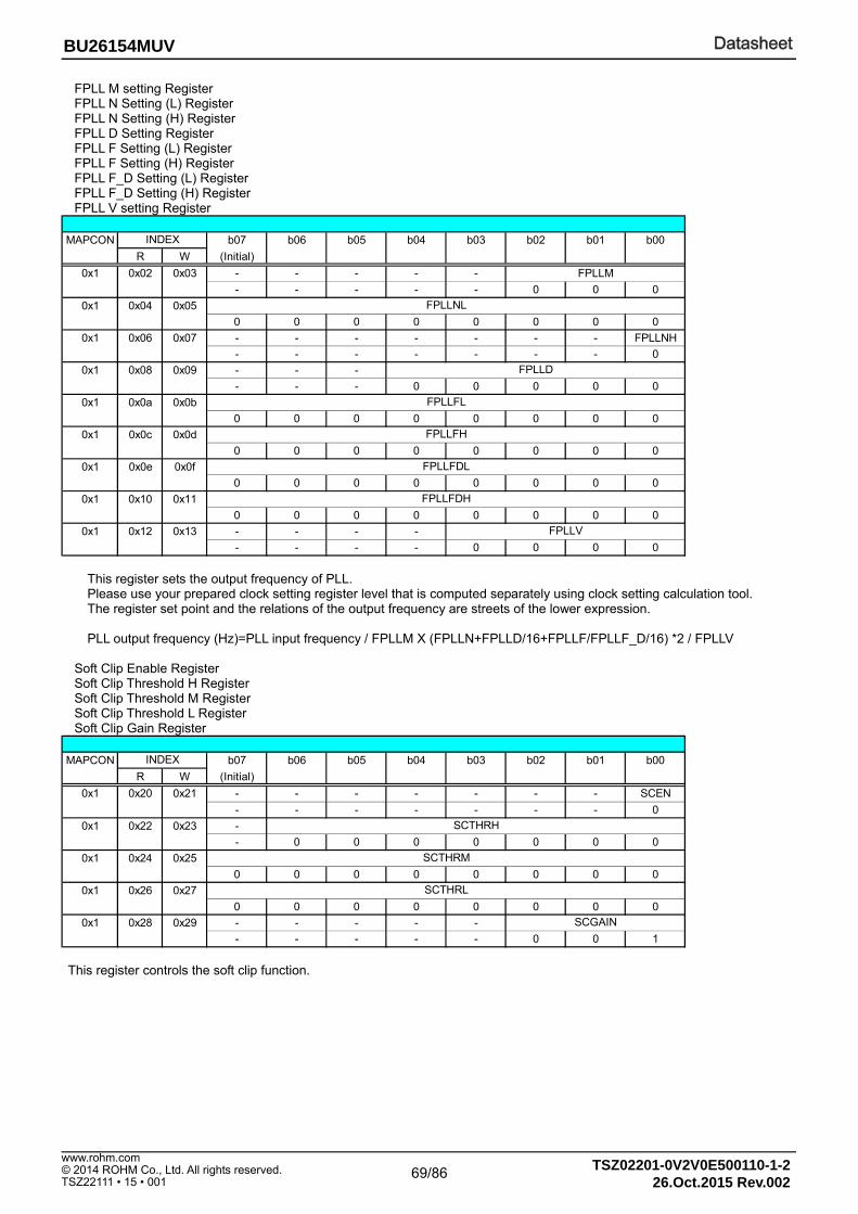
DatasheetDatasheet
69/86 TSZ02201-0V2V0E500110-1-2© 2014 ROHM Co., Ltd. All rights reserved.
26.Oct.2015 Rev.002
www.rohm.com
TSZ22111 • 15 • 001
BU26154MUV
FPLL M setting Register FPLL N Setting (L) Register FPLL N Setting (H) Register FPLL D Setting Register FPLL F Setting (L) Register FPLL F Setting (H) Register FPLL F_D Setting (L) Register FPLL F_D Setting (H) Register FPLL V setting Register
MAPCON b07 b06 b05 b04 b03 b02 b01 b00
R W (Initial)
0x1 0x02 0x03 - - - - -
- - - - - 0 0 0
0x1 0x04 0x05
0 0 0 0 0 0 0 0
0x1 0x06 0x07 - - - - - - - FPLLNH
- - - - - - - 0
0x1 0x08 0x09 - - -
- - - 0 0 0 0 0
0x1 0x0a 0x0b
0 0 0 0 0 0 0 0
0x1 0x0c 0x0d
0 0 0 0 0 0 0 0
0x1 0x0e 0x0f
0 0 0 0 0 0 0 0
0x1 0x10 0x11
0 0 0 0 0 0 0 0
0x1 0x12 0x13 - - - -
- - - - 0 0 0 0
FPLLV
FPLLFDH
FPLLFDL
FPLLFH
FPLLFL
FPLLD
FPLLNL
INDEX
FPLLM
This register sets the output frequency of PLL. Please use your prepared clock setting register level that is computed separately using clock setting calculation tool. The register set point and the relations of the output frequency are streets of the lower expression. PLL output frequency (Hz)=PLL input frequency / FPLLM X (FPLLN+FPLLD/16+FPLLF/FPLLF_D/16) *2 / FPLLV
Soft Clip Enable Register Soft Clip Threshold H Register Soft Clip Threshold M Register Soft Clip Threshold L Register Soft Clip Gain Register
MAPCON b07 b06 b05 b04 b03 b02 b01 b00
R W (Initial)
0x1 0x20 0x21 - - - - - - - SCEN
- - - - - - - 0
0x1 0x22 0x23 -
- 0 0 0 0 0 0 0
0x1 0x24 0x25
0 0 0 0 0 0 0 0
0x1 0x26 0x27
0 0 0 0 0 0 0 0
0x1 0x28 0x29 - - - - -
- - - - - 0 0 1
SCGAIN
SCTHRL
SCTHRM
INDEX
SCTHRH
This register controls the soft clip function.

DatasheetDatasheet
70/86 TSZ02201-0V2V0E500110-1-2© 2014 ROHM Co., Ltd. All rights reserved.
26.Oct.2015 Rev.002
www.rohm.com
TSZ22111 • 15 • 001
BU26154MUV
SCEN Sets the soft clip enable.
Setting Explanation 0 Disable 1 Enable
SCTHRH SCTHRM SCTHRL
This register sets the soft clip threshold level. When PCM signal with more than of this bit is input, the LSI clips it according to a value of SCGAIN and works. The value of threshold level is 23bit (SCTHRM [6:0], SCTHRM [7:0], and SCTHRL [7:0]) Please do not change the value of this bit during Soft Clip function movement. SCGAIN
This sets the magnification during soft clip. In addition, please do not change the value of this bit during movement. Setting Explanation
0x0 Double 0x1 1 time (default) 0x2 I double 1/2 0x3 I double 1/4 0x4 I double 1/8 0x5 I double 1/16 0x6 I double 1/32 0x7 I double 1/64
Touch ADC Control Register
MAPCON b07 b06 b05 b04 b03 b02 b01 b00
R W (Initial)
1 0x60 0x61 TCHEN TCHA2 TCHA1 TCHA0 - TCHRSEL TCHMODE -
0 1 1 1 1 0 0 -
INDEX
This register controls the touch panel interface, and a light, please do "1" in bit 3.
TCHEN This enables and disables the touch panel interface. In the case of "0", this bit is cleared after (an automatic mode in the case of enable), the lead of the AD conversion data of the touch panel interface TCHA2 bit by "0".
TCHEN Explanation 0x0 A touch panel interface is disabled. 0x1 A touch panel interface is enabled.
TCHA2
It controls the convert mode of the touch panel interface, and, in the case of "1", this bit interrupts it after the lead of the AD conversion data of the touch panel interface automatically and changes in a mode. The next conversion starts by an automatic mode leading AD conversion result in the case of disable.
TCHA2 Explanation 0x0 An automatic mode is enabled. 0x1 An automatic mode is disabled.
TCHA1, TCHA0
This controls the convert mode of the touch panel interface. TCHEN TCHA2 TCHA1, TCHA0 Explanation
TCHEN=1 * 0x0 It becomes the X-axis measurement mode. * 0x1 It becomes the Y-axis measurement mode. * 0x2 It becomes the Z1 axis measurement mode. * 0x3 It becomes the Z2 axis measurement mode.
TCHEN=0 0x0 0x3 It becomes the interrupt mode.

DatasheetDatasheet
71/86 TSZ02201-0V2V0E500110-1-2© 2014 ROHM Co., Ltd. All rights reserved.
26.Oct.2015 Rev.002
www.rohm.com
TSZ22111 • 15 • 001
BU26154MUV
TCHRSEL Choose interrupt pull up resistance using for one of a touch panel interface. TCHRSEL Explanation
0x0 I interrupt it, and pulling up resistance becomes 50kΩ. 0x1 I interrupt it, and pulling up resistance becomes 90kΩ.
TCHMODE
Choose touch panel interface mode. TCHMODE Explanation
0x0 12Bit Mode 0x1 8Bit Mode
Touch ADC result1 Register Touch ADC result2 Register
MAPCON b07 b06 b05 b04 b03 b02 b01 b00
R W (Initial)
0x1 0x62 0x63
0 0 0 0 0 0 0 0
0x1 0x64 0x65 - - - -
0 0 0 0 - - - -
ADCR2
ADCR1
INDEX
This register is to get analog-to-digital conversion data of the touch panel interface ADC. In the 12bit mode, please read register in order of ADCR1 ($62h), ADCR2 ($64h).
TOUTCHAD1 This register is to get analog-to-digital conversion data of the touch panel interface ADC. In the 8 bit mode, please read only this register. In the 12 bit mode, this register is higher 8 bits of the 12bit ADC output data.
TOUTCHAD2 This register is to get analog-to-digital conversion data of the touch panel interface ADC. In the 8 bit mode, this register value is "0". In the 12 bits mode, this register is lower 4 bits of the 12bit ADC output data.
Headphone Amplifier Input Control Register
MAPCON b07 b06 b05 b04 b03 b02 b01 b00
R W (Initial)
0x1 0x82 0x83 - - HPRIN2EN HPRIN1EN - - - HPLIN1EN
- - 0 0 - - - 0
INDEX
This register is to set the input path of the headphones amplifier. Please do not set HPRIN1EN bit and the HPRIN2EN bit to "1" simultaneously. Please set only either bit to " 1 ".
HPLIN1EN This bit is to set the input path of the Lch headphones amplifier. HPLIN1EN Explanation
0x0 Disconnect the output of Lch-DAC to Lch headphones amplifier. 0x1 Connect the output of Lch-DAC to Lch headphones amplifier.
HPRIN1EN
This bit is to set the input path of the Rch headphones amplifier. HPRIN1EN Explanation
0x0 Disconnect the output of Lch-DAC to Rch headphones amplifier. 0x1 Connect the output of Lch-DAC to Rch headphones amplifier.
HPRIN2EN
This bit is to set the input path of the Rch headphones amplifier. HPRIN2EN Explanation
0x0 Disconnect the output of Rch-DAC to Rch headphones amplifier. 0x1 Connect the output of Rch-DAC to Rch headphones amplifier.

DatasheetDatasheet
72/86 TSZ02201-0V2V0E500110-1-2© 2014 ROHM Co., Ltd. All rights reserved.
26.Oct.2015 Rev.002
www.rohm.com
TSZ22111 • 15 • 001
BU26154MUV
Speaker Amplifier Input Control Register
MAPCON b07 b06 b05 b04 b03 b02 b01 b00
R W (Initial)
0x1 0x84 0x85 - - - - SPIN2EN SPIN1EN
- - - - 0 0 0 0
INDEX
SPVOL
This register is to set the input path and the volume of the speaker amplifier.
SPVOL This register is to set the volume level of the speaker amplifier. SPVOL Explanation
0x0 0dB 0x1 6dB 0x2 12dB 0x3 18dB
SPIN1EN
This bit is to set the input path of the speaker amplifier. SPIN1EN Explanation
0x0 Disconnect the output of the Lch volume to a speaker amplifier. 0x1 Connect the output of the Lch volume to a speaker amplifier.
SPIN2EN
This bit is to set the input path of the speaker amplifier. SPIN2EN Explanation
0x0 Disconnect the output of the Rch volume to a speaker amplifier. 0x1 Connect the output of the Rch volume to a speaker amplifier.
Play Programmable LPF Setting Register
MAPCON b07 b06 b05 b04 b03 b02 b01 b00
R W (Initial)
0x1 0xa0 0xa1 - - - - - - PLPFOD PLPFEN
- - - - - - 0 0
INDEX
This register is to set “LPF” block for DAC-path (playback) in digital signal flow. This is to set Enable/Disable and filter order. This function is effective for DAC-path (playback) at “PLPFEN=1” and “SEMODE [7] =1”.
PLPFEN
This bit is to set Enable/Disable of low pass filter for DAC-path. PLPFEN Explanation
0 LPF for DAC-path is Disable 1 LPF for DAC-path is Enable
PLPFOD
This bit is to set number of low pass filter order for DAC-path. PLPFOD Explanation
0 LPF for DAC-path is second-order 1 LPF for DAC-path is first-order
Play Programmable LPF Coef (L) Register Play Programmable LPF Coef (H) Register
MAPCON b07 b06 b05 b04 b03 b02 b01 b00
R W (Initial)
0x1 0xa2 0xa3
0 0 0 0 0 0 0 0
0x1 0xa4 0xa5
0 0 0 0 0 0 0 0
PLPFC0H
PLPFC0L
INDEX
This register is to set “LPF” block for DAC-path (playback) in digital signal flow. This is to set Enable/Disable and filter order.

DatasheetDatasheet
73/86 TSZ02201-0V2V0E500110-1-2© 2014 ROHM Co., Ltd. All rights reserved.
26.Oct.2015 Rev.002
www.rohm.com
TSZ22111 • 15 • 001
BU26154MUV
PLPFC0L [7:0] / PLPFCOH [7:0] This bit is to set low pass filter cut off frequency for DAC-path. This value has to change by sampling frequency. Please use Filter Setting Calculation program for *PLPFC0L / PLPFC0H setting.
Rec Programmable LPF Setting Register
MAPCON b07 b06 b05 b04 b03 b02 b01 b00
R W (Initial)
0x1 0xa6 0xa7 - - - - - - RLPFOD RLPFEN
- - - - - - 0 0
INDEX
This register is to set “LPF” block for ADC-path (record) in digital signal flow. This is to set Enable/Disable and filter order. This function is exclusive to “HPF2” controlled by HPF2EN of DSP Filter Function Enable register. This function is effective for ADC-path (record) at “RLPFEN=1” and “SEMODE [7] =1”.
RLPFEN This bit is to set Enable/Disable of low pass filter for ADC-path. RLPFEN Explanation
0 LPF for DAC-path is Disable (HPF2 is available) 1 LPF for DAC-path is Enable (HPF2 is not available. HPF2EN-bit
is not valid) RLPFOD This bit is to set number of low pass filter order for ADC-path. RLPFOD Explanation
0 LPF for ADC-path is second-order 1 LPF for ADC-path is first-order
Rec Programmable LPF Coef (L) Register Rec Programmable LPF Coef (H) Register
MAPCON b07 b06 b05 b04 b03 b02 b01 b00
R W (Initial)
0x1 0xa8 0xa9
0 0 0 0 0 0 0 0
0x1 0xaa 0xab
0 0 0 0 0 0 0 0
RLPFC0H
INDEX
RLPFC0L
This register is to set “LPF” block for ADC-path (playback) in digital signal flow.
Audio Analog Control2 Register
HPLSEN
This bit controls the level shifter for headphone amplifier. Setting Explanation
0x0 Disable the level shifter for headphone amplifier 0x1 Enable the level shifter for headphone amplifier
Audio Analog Control1 Register
MAPCON b07 b06 b05 b04 b03 b02 b01 b00R W (initial)
0x02 0x12 0x13 - - - - - - - AREFI1EN- - - - - - - 1
INDEX
MAPCON b07 b06 b05 b04 b03 b02 b01 b00R W (initial)
0x02 0x04 0x05 - - - - HPLSEN - - -- - 1 - 1 1 - -
INDEX
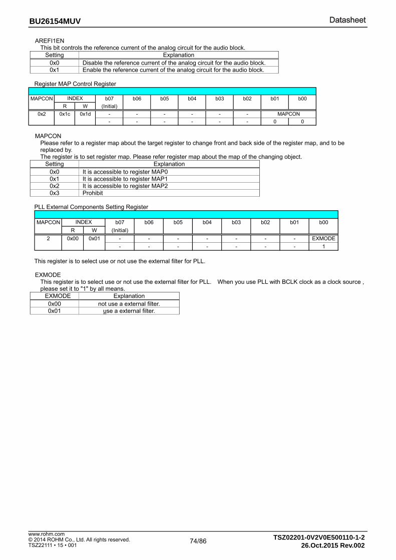
DatasheetDatasheet
74/86 TSZ02201-0V2V0E500110-1-2© 2014 ROHM Co., Ltd. All rights reserved.
26.Oct.2015 Rev.002
www.rohm.com
TSZ22111 • 15 • 001
BU26154MUV
AREFI1EN This bit controls the reference current of the analog circuit for the audio block.
Setting Explanation 0x0 Disable the reference current of the analog circuit for the audio block. 0x1 Enable the reference current of the analog circuit for the audio block.
Register MAP Control Register
MAPCON b07 b06 b05 b04 b03 b02 b01 b00
R W (Initial)
0x2 0x1c 0x1d - - - - - -
- - - - - - 0 0
INDEX
MAPCON
MAPCON Please refer to a register map about the target register to change front and back side of the register map, and to be replaced by. The register is to set register map. Please refer register map about the map of the changing object.
Setting Explanation 0x0 It is accessible to register MAP0 0x1 It is accessible to register MAP1 0x2 It is accessible to register MAP2 0x3 Prohibit
PLL External Components Setting Register
MAPCON b07 b06 b05 b04 b03 b02 b01 b00
R W (Initial)
2 0x00 0x01 - - - - - - - EXMODE
- - - - - - - 1
INDEX
This register is to select use or not use the external filter for PLL. EXMODE
This register is to select use or not use the external filter for PLL. When you use PLL with BCLK clock as a clock source , please set it to "1" by all means.
EXMODE Explanation 0x00 not use a external filter. 0x01 use a external filter.
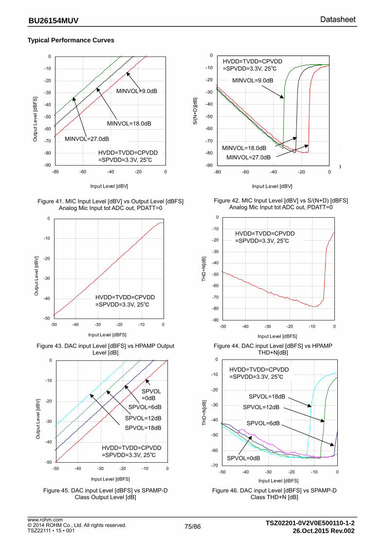
DatasheetDatasheet
75/86 TSZ02201-0V2V0E500110-1-2© 2014 ROHM Co., Ltd. All rights reserved.
26.Oct.2015 Rev.002
www.rohm.com
TSZ22111 • 15 • 001
BU26154MUV
Typical Performance Curves
-70
-60
-50
-40
-30
-20
-10
0
-50 -40 -30 -20 -10 0
Input Level [dBFS]
TH
D+
N[d
B]
-50
-40
-30
-20
-10
0
-50 -40 -30 -20 -10 0
Input Level [dBFS]
Ou
tpu
t Le
vel [
dB
V]
-90
-80
-70
-60
-50
-40
-30
-20
-10
0
-50 -40 -30 -20 -10 0
Input Level [dBFS]
TH
D+
N[d
B]
-50
-40
-30
-20
-10
0
-50 -40 -30 -20 -10 0
Input Level [dBFS]
Ou
tpu
t Le
vel [
dB
V]
-90
-80
-70
-60
-50
-40
-30
-20
-10
0
-80 -60 -40 -20 0
Input Level [dBV]
Ou
tpu
t Le
vel [
dB
FS
]
Figure 41. MIC Input Level [dBV] vs Output Level [dBFS]Analog Mic Input tot ADC out, PDATT=0
Figure 43. DAC input Level [dBFS] vs HPAMP Output Level [dB]
LALCMXGAIN=6.0dB
LALCMXGAIN=-9.0dB
HVDD1=IOVDD=SPLVDD =SPRVDD=3.3V, 25
MINVOL=27.0dB
MINVOL=18.0dB
MINVOL=9.0dB
-90
-80
-70
-60
-50
-40
-30
-20
-10
0
-80 -60 -40 -20 0
Input Level [dBV]
S/(N
+D
)[dB
]
HVDD=TVDD=CPVDD =SPVDD=3.3V, 25
MINVOL=27.0dB
MINVOL=18.0dB
MINVOL=9.0dB
HVDD=TVDD=CPVDD =SPVDD=3.3V, 25
HVDD=TVDD=CPVDD =SPVDD=3.3V, 25
Figure 42. MIC Input Level [dBV] vs S/(N+D) [dBFS] Analog Mic Input tot ADC out, PDATT=0
HVDD=TVDD=CPVDD =SPVDD=3.3V, 25
Figure 44. DAC input Level [dBFS] vs HPAMP THD+N[dB]
Figure 45. DAC input Level [dBFS] vs SPAMP-D Class Output Level [dB]
HVDD=TVDD=CPVDD=SPVDD=3.3V, 25
Figure 46. DAC input Level [dBFS] vs SPAMP-D Class THD+N [dB]
HVDD=TVDD=CPVDD =SPVDD=3.3V, 25
SPVOL=18dB
SPVOL=12dB
SPVOL=6dB
SPVOL=0dB
SPVOL=18dB
SPVOL=0dB
SPVOL=6dB
SPVOL=12dB

DatasheetDatasheet
76/86 TSZ02201-0V2V0E500110-1-2© 2014 ROHM Co., Ltd. All rights reserved.
26.Oct.2015 Rev.002
www.rohm.com
TSZ22111 • 15 • 001
BU26154MUV
-50
-40
-30
-20
-10
0
-50 -40 -30 -20 -10 0
Input Level [dBFS]
Ou
tpu
t Le
vel [
dB
V]
Figure 47. DAC input Level [dBFS] vs SPAMP-AB Class Output Level [dB]
SPVOL=18dB
SPVOL=12dB
SPVOL=6dB
SPVOL=0dB
-70
-60
-50
-40
-30
-20
-10
0
-50 -40 -30 -20 -10 0
Input Level [dBFS]
TH
D+
N[d
B]
Figure 48. DAC input Level [dBFS] vs SPAMP-AB Class THD+N [dB]
SPVOL=6dB
SPVOL=12dB
SPVOL=18dB
SPVOL=0dB
HVDD=TVDD=CPVDD =SPVDD=3.3V, 25
HVDD=TVDD=CPVDD =SPVDD=3.3V, 25

DatasheetDatasheet
77/86 TSZ02201-0V2V0E500110-1-2© 2014 ROHM Co., Ltd. All rights reserved.
26.Oct.2015 Rev.002
www.rohm.com
TSZ22111 • 15 • 001
BU26154MUV
Power dissipation
Measuring instrument: TH-156 (Kuwano Electrical) Measuring status: PCB mounting(Rohm) PCB size: 74.2mm × 74.2mm × 1.6mm (PCB with thermal via) The quarity of the material: FR4 The part of package bottom exposure heat sink connected PCB by solder. PCB (1): 1-layer board (Size of copper foil on bottom: 23.69mm2), θja = 125.0/W PCB (2): 4-layer board (Size of copper foil on top and bottom: 23.69mm2, 2nd and 3rd layer Size of copper foil on bottom: 5505mm2), θja = 33.2/W PCB (3): 4-layer board (Size of copper foil on bottom: 5505mm2), θja = 27.4/W
Please consider power dissipation by an actual using status, and perform the thermal design which has a margin enough. Although this product is exposing the frame on the bottom side of a package, heat dissipation processing is performed to this portion, and we assume raising and using heat dissipation efficiency. Please use not only PCB-top pattern but also PCB-bottom pattern, taking heat dissipation pattern as large as possible at it. Although D-class speaker amplifier have very high efficiency compared with the conventional analog-speaker amplifier and there is also little generation of heat, when continuous action is carried out by the maximum output power, actual power dissipation may exceed Pd. Please consider the thermal design enough so that power dissipation of averaging output power does not exceed Pd. (Tjmax : Maximum junction temperature=125, Ta :Ambient temperature[], θja :Package thermal registance[/W], Poav:Averaging output power[W], η:Efficiency) Package Power dissipation Pd (W) = (Tjmax - Ta)/ θja Circuit Power dissipation Pdiss(W) = Poav * (1 / η- 1)
Figure 49.VQFN040V6060 Package
0.00
0.50
1.00
1.50
2.00
2.50
3.00
3.50
4.00
0 20 40 60 80 100 120 140
ambient temperature : Ta()
pow
er
dis
sapation (
W)

DatasheetDatasheet
78/86 TSZ02201-0V2V0E500110-1-2© 2014 ROHM Co., Ltd. All rights reserved.
26.Oct.2015 Rev.002
www.rohm.com
TSZ22111 • 15 • 001
BU26154MUV
I/O equivalence circuit(s) Terminal
No. Terminal
Name Terminal
I/O Terminal Power
Equivalent Circuit
1 40
HPL HPR
O HPVDD
2 HPVDD O CPVDD
4 HPVSS O CPVDD
5 CPN O CPVDD
6 SPVDD - SPVDD
7 8
SDOUT+ SPOUT-
O SPVDD
HPVSS
HPVDD
CPGND
CPVDD
CPGND
CPGND CPN
HPVSS
CPGND
HPVSS
SPGND
SPVDD
SPGND

DatasheetDatasheet
79/86 TSZ02201-0V2V0E500110-1-2© 2014 ROHM Co., Ltd. All rights reserved.
26.Oct.2015 Rev.002
www.rohm.com
TSZ22111 • 15 • 001
BU26154MUV
Terminal
No. Terminal
Name Terminal
I/O Terminal Power
Equivalent Circuit
9 SPGND - -
10 VMID O REGOUT
11 MICBIAS CAP O HVDD
12 13
MIN1 MIN2
I REGOUT
14 HGND2 - -
15 HGND1 - -
16 N.C - -
SPVDD
REGOUT
REGOUT
HGND2
HGND2
HGND2 HGND2
HVDD
REGOUT
HGND1
REGOUT HVDD
REGOUT HVDD

DatasheetDatasheet
80/86 TSZ02201-0V2V0E500110-1-2© 2014 ROHM Co., Ltd. All rights reserved.
26.Oct.2015 Rev.002
www.rohm.com
TSZ22111 • 15 • 001
BU26154MUV
Terminal
No. Terminal
Name Terminal
I/O Terminal Power
Equivalent Circuit
17 HVDD - HVDD
18 REGOUT - HVDD
19 PLLC O REGOUT
20 RESETB I HVDD
21 30
TSTO IRQB
O HVDD
22 23 25 28
MCLKI CSB/SCL
SCLK/SAD SAI_SDIN
I HVDD
HGND1
HGND1
HVDD
HGND1
HGND1
HGND2
REGOUT
HVDD
HGND1
HVDD
HGND1HGND1
HVDD
HGND1HGND1
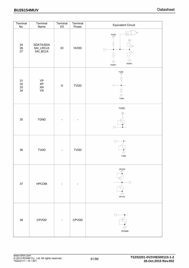
DatasheetDatasheet
81/86 TSZ02201-0V2V0E500110-1-2© 2014 ROHM Co., Ltd. All rights reserved.
26.Oct.2015 Rev.002
www.rohm.com
TSZ22111 • 15 • 001
BU26154MUV
Terminal
No. Terminal
Name Terminal
I/O Terminal Power
Equivalent Circuit
24 26 27
SDATA/SDA SAI_LRCLK SAI_BCLK
IO HVDD
31 32 33 34
YP XP XN YN
O TVDD
35 TGND - -
36 TVDD - TVDD
37 HPCOM - -
38 CPVDD - CPVDD
HVDD
HGND1HGND1
TVDD
TGND
TVDD
TGND
HPVDD
HPVSS
CPGND

DatasheetDatasheet
82/86 TSZ02201-0V2V0E500110-1-2© 2014 ROHM Co., Ltd. All rights reserved.
26.Oct.2015 Rev.002
www.rohm.com
TSZ22111 • 15 • 001
BU26154MUV
Terminal
No. Terminal
Name Terminal
I/O Terminal Power
Equivalent Circuit
39 CPP - CPVDD
CPVDD
CPGND
DatasheetDatasheet
83/86 TSZ02201-0V2V0E500110-1-2© 2014 ROHM Co., Ltd. All rights reserved.
26.Oct.2015 Rev.002
www.rohm.com
TSZ22111 • 15 • 001
BU26154MUV
Operational Notes
1) Absolute Maximum Ratings An excess in the absolute maximum ratings, such as supply voltage, temperature range of operating conditions, etc., can break down devices, thus don’t exceed the absolute maximum ratings of supply voltage, temperature. If any special mode exceeding the absolute maximum ratings is assumed, consideration should be given to take physical safety measures including the use of fuses, etc.
2) GND voltage Make setting of the potential of the GND terminal so that it will be maintained at the minimum in any operating state.
3) Short circuit between terminals and erroneous mounting In order to mount ICs on a set PCB, pay thorough attention to the direction and offset of the ICs. Erroneous mounting can break down the ICs. Furthermore, if a short circuit occurs due to foreign matters entering between terminals or between the terminal and the power supply or the GND terminal, the ICs can break down.
4) Operation in strong electromagnetic field Be noted that using ICs in the strong electromagnetic field can malfunction them.
5) Thermal design If use speaker amplifier function, please consider power dissipation by an actual using status, and perform the thermal design which have a margin enough. If an input signal is made excessive in the state with insufficient heat dissipation, desired output power may not only be securable, but the thermal shutdown may operate.
6) Thermal shutdown This IC has the thermal shutdown circuit. If the thermal shutdown operates, speaker output terminal and line output terminal will stop in the open state(high inpedance state).The thermal shutdown is only a function for suspending the output operation of IC to the last at the time of the thermal run-away under the abnormal condition in which chip temperature(Tjmax) exceeded 170 degrees. It is a circuit to protect IC, and the purpose is not offering protection and a guarantee of the set.
7) Short protection of output terminals This IC has the short protect function for output terminals. If the short protect function operates, output terminal will be latched and stop in the open state(high inpedance state).After a stop, even if a short state is removed, it does not return to normal operation automatically. Please once turn off a power supply or a shutdown signal to make it return, and let turn on again and reboot.
8) Operating condition Operating voltage and operating temperature are ranges which perform basic function. Electrical characteristics and absolute maximum rating are not guaranteed in full voltage range or full temperature range.
9) Electrical characteristics specification Each audio characteristic specification, such as limit output power, total harmonic distortion shows the standard performance of the device, and depends for it on board layout / use parts / power supply part greatly. Typical specification value is a value when a device and each parts are directly mounted in the board of Rohm's standard.
10) Power supply Large peak current rushes into a SPVDD power supply line at the time of ClassD speaker amplifier use. The audio characteristic is affected by the value of a power supply decoupling capacitor, and layout. The power supply decoupling capacitor should be layouted (1uF or more) with sufficiently low ESR (equivalent series resistance) to most close of IC terminal. Moreover, in the design of a board pattern, the wiring of a power supply / GND line should become low impedance. In that case, even if digital power supply and analog power supply are same potential, please devide the digital power pattern and the analog power pattern and reduce a surroundings lump of the digital noise to the analog power supply by the common impedance of a wiring pattern. Please take the same pattern design into consideration also about a GND line. Moreover, while inserting a capacitor between power supply-GND terminals about all the power supply terminals of LSI, and please determine the value of capacitor after sufficient confirmation that there is no problem in the characteristics of capacitors to be used (a capacity omission happens at low temperature) in the case of electrolytic capacitors use.
11) External capacitor
In order to use a ceramic capacitor as the external capacitor, determine the constant with consideration given to a degradation in the nominal capacitance due to DC bias and changes in the capacitance due to temperature, etc.
12) Status of this document

DatasheetDatasheet
84/86 TSZ02201-0V2V0E500110-1-2© 2014 ROHM Co., Ltd. All rights reserved.
26.Oct.2015 Rev.002
www.rohm.com
TSZ22111 • 15 • 001
BU26154MUV
The Japanese version of this document is formal specification. A customer may use this translation version only for a reference to help reading the formal version. If there are any differences in translation version of this document formal version takes priority.

DatasheetDatasheet
85/86 TSZ02201-0V2V0E500110-1-2© 2014 ROHM Co., Ltd. All rights reserved.
26.Oct.2015 Rev.002
www.rohm.com
TSZ22111 • 15 • 001
BU26154MUV
Ordering Information
B U 2 6 1 5 4 M U V - E 2
Part Number
Package MUV:VQFP040V6060
Packaging and forming specification E2: Embossed tape and reel
Physical Dimension, Tape and Reel Information
Package Name VQFN040V6060
Marking Diagrams
VQFN040V6060 (TOP VIEW)
BU26154
Part Number Marking
LOT Number
1PIN MARK
∗ Order quantity needs to be multiple of the minimum quantity.
<Tape and Reel information>
Embossed carrier tapeTape
Quantity
Direction of feed
The direction is the 1pin of product is at the upper left when you hold reel on the left hand and you pull out the tape on the right hand
2000pcs
E2
( )
Direction of feed
Reel1pin

DatasheetDatasheet
86/86 TSZ02201-0V2V0E500110-1-2© 2014 ROHM Co., Ltd. All rights reserved.
26.Oct.2015 Rev.002
www.rohm.com
TSZ22111 • 15 • 001
BU26154MUV
Revision History
Date Revision Changes
23.Jun.2014 001 Rev.001 First revision release26.Oct.2015 002 P1. Change the Height of Package
P4. Change the application circuit P13. Change the VMIC reference voltage (SPVDD=> HVDD) P38, P48,P49,P50,P51,P73 Register function explanation and register details explanation - Removed MCLKOE bit and ADCREN bit、 - Added Analog Input Power Management, Speaker Amplifier Power Management registers
MAPCON setting - Changed ZCEN explanation(PDATT => EFFECT VOLUME) - Added the explanation of Playback Digital Attenuator Control Register /B “FFh setting” - Changed HPLSEN bit of Audio analog contol2 register

DatasheetDatasheet
Notice-PGA-E Rev.002© 2015 ROHM Co., Ltd. All rights reserved.
Notice Precaution on using ROHM Products
1. Our Products are designed and manufactured for application in ordinary electronic equipments (such as AV equipment, OA equipment, telecommunication equipment, home electronic appliances, amusement equipment, etc.). If you intend to use our Products in devices requiring extremely high reliability (such as medical equipment (Note 1), transport equipment, traffic equipment, aircraft/spacecraft, nuclear power controllers, fuel controllers, car equipment including car accessories, safety devices, etc.) and whose malfunction or failure may cause loss of human life, bodily injury or serious damage to property (“Specific Applications”), please consult with the ROHM sales representative in advance. Unless otherwise agreed in writing by ROHM in advance, ROHM shall not be in any way responsible or liable for any damages, expenses or losses incurred by you or third parties arising from the use of any ROHM’s Products for Specific Applications.
(Note1) Medical Equipment Classification of the Specific Applications JAPAN USA EU CHINA
CLASSⅢ CLASSⅢ
CLASSⅡb CLASSⅢ
CLASSⅣ CLASSⅢ
2. ROHM designs and manufactures its Products subject to strict quality control system. However, semiconductor
products can fail or malfunction at a certain rate. Please be sure to implement, at your own responsibilities, adequate safety measures including but not limited to fail-safe design against the physical injury, damage to any property, which a failure or malfunction of our Products may cause. The following are examples of safety measures:
[a] Installation of protection circuits or other protective devices to improve system safety [b] Installation of redundant circuits to reduce the impact of single or multiple circuit failure
3. Our Products are designed and manufactured for use under standard conditions and not under any special or extraordinary environments or conditions, as exemplified below. Accordingly, ROHM shall not be in any way responsible or liable for any damages, expenses or losses arising from the use of any ROHM’s Products under any special or extraordinary environments or conditions. If you intend to use our Products under any special or extraordinary environments or conditions (as exemplified below), your independent verification and confirmation of product performance, reliability, etc, prior to use, must be necessary:
[a] Use of our Products in any types of liquid, including water, oils, chemicals, and organic solvents [b] Use of our Products outdoors or in places where the Products are exposed to direct sunlight or dust [c] Use of our Products in places where the Products are exposed to sea wind or corrosive gases, including Cl2,
H2S, NH3, SO2, and NO2
[d] Use of our Products in places where the Products are exposed to static electricity or electromagnetic waves [e] Use of our Products in proximity to heat-producing components, plastic cords, or other flammable items [f] Sealing or coating our Products with resin or other coating materials [g] Use of our Products without cleaning residue of flux (even if you use no-clean type fluxes, cleaning residue of
flux is recommended); or Washing our Products by using water or water-soluble cleaning agents for cleaning residue after soldering
[h] Use of the Products in places subject to dew condensation
4. The Products are not subject to radiation-proof design. 5. Please verify and confirm characteristics of the final or mounted products in using the Products. 6. In particular, if a transient load (a large amount of load applied in a short period of time, such as pulse. is applied,
confirmation of performance characteristics after on-board mounting is strongly recommended. Avoid applying power exceeding normal rated power; exceeding the power rating under steady-state loading condition may negatively affect product performance and reliability.
7. De-rate Power Dissipation depending on ambient temperature. When used in sealed area, confirm that it is the use in
the range that does not exceed the maximum junction temperature. 8. Confirm that operation temperature is within the specified range described in the product specification. 9. ROHM shall not be in any way responsible or liable for failure induced under deviant condition from what is defined in
this document.
Precaution for Mounting / Circuit board design 1. When a highly active halogenous (chlorine, bromine, etc.) flux is used, the residue of flux may negatively affect product
performance and reliability.
2. In principle, the reflow soldering method must be used on a surface-mount products, the flow soldering method must be used on a through hole mount products. If the flow soldering method is preferred on a surface-mount products, please consult with the ROHM representative in advance.
For details, please refer to ROHM Mounting specification

DatasheetDatasheet
Notice-PGA-E Rev.002© 2015 ROHM Co., Ltd. All rights reserved.
Precautions Regarding Application Examples and External Circuits 1. If change is made to the constant of an external circuit, please allow a sufficient margin considering variations of the
characteristics of the Products and external components, including transient characteristics, as well as static characteristics.
2. You agree that application notes, reference designs, and associated data and information contained in this document
are presented only as guidance for Products use. Therefore, in case you use such information, you are solely responsible for it and you must exercise your own independent verification and judgment in the use of such information contained in this document. ROHM shall not be in any way responsible or liable for any damages, expenses or losses incurred by you or third parties arising from the use of such information.
Precaution for Electrostatic
This Product is electrostatic sensitive product, which may be damaged due to electrostatic discharge. Please take proper caution in your manufacturing process and storage so that voltage exceeding the Products maximum rating will not be applied to Products. Please take special care under dry condition (e.g. Grounding of human body / equipment / solder iron, isolation from charged objects, setting of Ionizer, friction prevention and temperature / humidity control).
Precaution for Storage / Transportation 1. Product performance and soldered connections may deteriorate if the Products are stored in the places where:
[a] the Products are exposed to sea winds or corrosive gases, including Cl2, H2S, NH3, SO2, and NO2 [b] the temperature or humidity exceeds those recommended by ROHM [c] the Products are exposed to direct sunshine or condensation [d] the Products are exposed to high Electrostatic
2. Even under ROHM recommended storage condition, solderability of products out of recommended storage time period may be degraded. It is strongly recommended to confirm solderability before using Products of which storage time is exceeding the recommended storage time period.
3. Store / transport cartons in the correct direction, which is indicated on a carton with a symbol. Otherwise bent leads
may occur due to excessive stress applied when dropping of a carton. 4. Use Products within the specified time after opening a humidity barrier bag. Baking is required before using Products of
which storage time is exceeding the recommended storage time period.
Precaution for Product Label QR code printed on ROHM Products label is for ROHM’s internal use only.
Precaution for Disposition When disposing Products please dispose them properly using an authorized industry waste company.
Precaution for Foreign Exchange and Foreign Trade act Since concerned goods might be fallen under listed items of export control prescribed by Foreign exchange and Foreign trade act, please consult with ROHM in case of export.
Precaution Regarding Intellectual Property Rights 1. All information and data including but not limited to application example contained in this document is for reference
only. ROHM does not warrant that foregoing information or data will not infringe any intellectual property rights or any other rights of any third party regarding such information or data.
2. ROHM shall not have any obligations where the claims, actions or demands arising from the combination of the Products with other articles such as components, circuits, systems or external equipment (including software).
3. No license, expressly or implied, is granted hereby under any intellectual property rights or other rights of ROHM or any third parties with respect to the Products or the information contained in this document. Provided, however, that ROHM will not assert its intellectual property rights or other rights against you or your customers to the extent necessary to manufacture or sell products containing the Products, subject to the terms and conditions herein.
Other Precaution 1. This document may not be reprinted or reproduced, in whole or in part, without prior written consent of ROHM.
2. The Products may not be disassembled, converted, modified, reproduced or otherwise changed without prior written consent of ROHM.
3. In no event shall you use in any way whatsoever the Products and the related technical information contained in the Products or this document for any military purposes, including but not limited to, the development of mass-destruction weapons.
4. The proper names of companies or products described in this document are trademarks or registered trademarks of ROHM, its affiliated companies or third parties.

DatasheetDatasheet
Notice – WE Rev.001© 2015 ROHM Co., Ltd. All rights reserved.
General Precaution 1. Before you use our Pro ducts, you are requested to care fully read this document and fully understand its contents.
ROHM shall n ot be in an y way responsible or liabl e for fa ilure, malfunction or acci dent arising from the use of a ny ROHM’s Products against warning, caution or note contained in this document.
2. All information contained in this docume nt is current as of the issuing date and subj ect to change without any prior
notice. Before purchasing or using ROHM’s Products, please confirm the la test information with a ROHM sale s representative.
3. The information contained in this doc ument is provi ded on an “as is” basis and ROHM does not warrant that all
information contained in this document is accurate an d/or error-free. ROHM shall not be in an y way responsible or liable for any damages, expenses or losses incurred by you or third parties resulting from inaccuracy or errors of or concerning such information.