mono- and bimetallic nanoparticles in sensor and catalysis
TRANSCRIPT

Mono- and bimetallic nanoparticles in sensor and catalysis devices
Section: Nanomaterials for sensoristic applications
Sergey Dubkov, [email protected]
2020

Historical Note
Zelenograd foundation date – 1958
MIET foundation date - 1965
USSR Minister of Electronic Industry -Alexander Shokin
Historical Note
ADVANCED MATERIALS AND TECHNOLOGIES (AM&T)
1
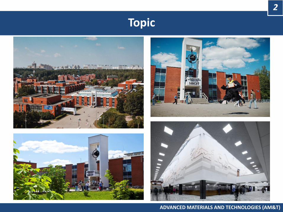
Historical NoteTopic
ADVANCED MATERIALS AND TECHNOLOGIES (AM&T)
2

Historical NoteZelenograd
ADVANCED MATERIALS AND TECHNOLOGIES (AM&T)
3
• literally “green town”• location: 20 km northwest of
Moscow• founded 1958• center of the microelectronics
industry • free economic zone• innovations-oriented
manufacturers
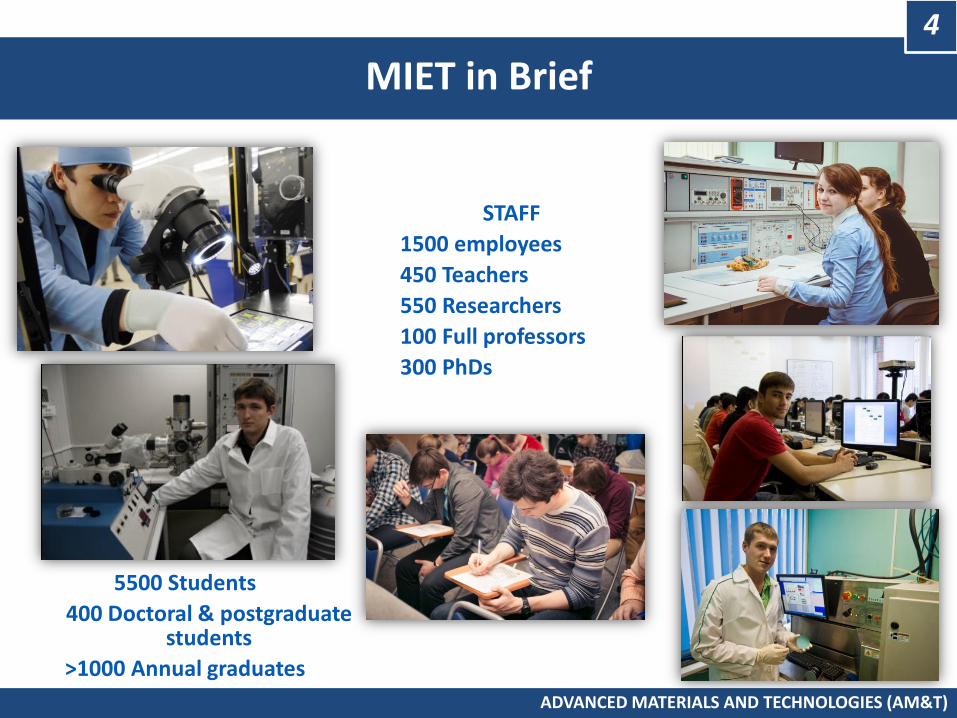
Historical NoteMIET in Brief
ADVANCED MATERIALS AND TECHNOLOGIES (AM&T)
4
STAFF
• 1500 employees
• 450 Teachers
• 550 Researchers
• 100 Full professors
• 300 PhDs
• 5500 Students
• 400 Doctoral & postgraduate students
• >1000 Annual graduates
Historical NoteMIET Research Activities
ADVANCED MATERIALS AND TECHNOLOGIES (AM&T)
5
Fundamental research in mathematics, physics, chemistry and electronics;
Information technologies and telecommunications;
Materials for micro-, nano- and optoelectronics;
Micro- and nanoelectronic devices;
Microsystem technology;
Devices of fiber and integrated optics;
Information control systems and complexes;
Microelectronic radio systems and devices;
Ecology and human life-support systems;
Economics, management and marketing;
Social and philosophical problems of science and engineering;
Problems of general and professional education.

Historical NoteSynthesis of new functional nanomaterials
ADVANCED MATERIALS AND TECHNOLOGIES (AM&T)
6
Nanoporous/nanotubularAnodic metal oxides and
semiconductors
Thin films andnanoclusters
Nanotubes, Nanorods,Nanowires

Historical Note
Application of metal nanoparticles
ADVANCED MATERIALS AND TECHNOLOGIES (AM&T)
7

Historical NoteSurface-enhanced Raman scattering (SERS)
ADVANCED MATERIALS AND TECHNOLOGIES (AM&T)
8
Schematic representation of the SERS effect (a) and comparison of the Raman spectra obtained in the presence and absence of gold nanoparticles (b)
(A) (B)

Historical NoteMethods of forming nanoparticle arrays
ADVANCED MATERIALS AND TECHNOLOGIES (AM&T)
9
Chemical liquid methods
TEM image of a cluster of Fe3O4 (a) nanoparticles obtained by deposition from a colloidal solution on a solid surface [1], SEM image of an array of gold disks (b) formed using electron beam lithography [2]
KSERS ≤ 104 KSERS ≤ 1012
Electron beam lithography• surface contamination of nanoparticles;• low reproducibility of arrays;• heterogeneity of the distribution of particles on the surface.
• high labor intensity and cost
(а) (b)
[1] Zhaoyang Tong, et al. Sensors. – 2016. – V. 16. – P. 308. [2] Madsen S., et al. Microscopy and Microanalysis. – 2013. – Vol. 19. – P. 1554-1555.
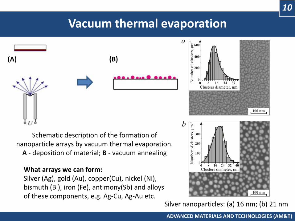
Historical NoteVacuum thermal evaporation
ADVANCED MATERIALS AND TECHNOLOGIES (AM&T)
10
(A) (B)
Schematic description of the formation of nanoparticle arrays by vacuum thermal evaporation.
A - deposition of material; B - vacuum annealing
Silver nanoparticles: (a) 16 nm; (b) 21 nm
What arrays we can form:Silver (Ag), gold (Au), copper(Cu), nickel (Ni), bismuth (Bi), iron (Fe), antimony(Sb) and alloys of these components, e.g. Ag-Cu, Ag-Au etc.

Historical NoteAu nanoparticle arrays of various average size
ADVANCED MATERIALS AND TECHNOLOGIES (AM&T)
11
TEM micrographs of gold nanoparticles with different geometrical parameters of arrays and corresponding histograms of particle size distribution
7 nm 12 nm 23 nm
Diameter NPs, nm Diameter NPs, nm Diameter NPs, nm
Nu
mb
er o
f p
arti
cles
, μm
2
Nu
mb
er
of
par
ticl
es
Nu
mb
er o
f p
arti
cles
, μm
2
Nu
mb
er o
f p
arti
cles
, μm
2

Historical NoteDepending position plasmon resonance on geometrical parameters
arrays Ag and Au
ADVANCED MATERIALS AND TECHNOLOGIES (AM&T)
12
Transmission spectra of arrays of Ag (a) and Au (b) nanoparticles formed on glass with different average particle sizes
Ag(а) (б)
Au
Wavelength, nm Wavelength, nm
Tran
smis
sio
n
Tran
smis
sio
n
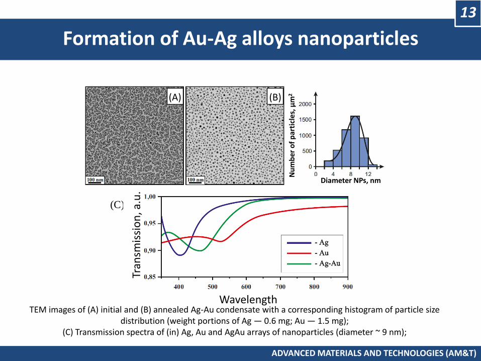
Historical NoteFormation of Au-Ag alloys nanoparticles
ADVANCED MATERIALS AND TECHNOLOGIES (AM&T)
13
TEM images of (A) initial and (B) annealed Ag-Au condensate with a corresponding histogram of particle size distribution (weight portions of Ag — 0.6 mg; Au — 1.5 mg);
(C) Transmission spectra of (in) Ag, Au and AgAu arrays of nanoparticles (diameter ~ 9 nm);
(A) (B)
(C)
Wavelength
Tran
smis
sio
n, a
.u.
Diameter NPs, nm
Nu
mb
er o
f p
arti
cles
, μm
2

Historical NotePlanar SERS substrate. The object of study is
amorphous carbon (a-C)
ADVANCED MATERIALS AND TECHNOLOGIES (AM&T)
14
SEM images of the surface of the SERS substratebefore (A) and after (B) the deposition of a layer of amorphous carbon
Raman spectra of amorphous carbon films (~ 25 nm) on glass and on a SERS substrate
at λL = 488 nm
SERS substrate design scheme
Raman shift, cm-1In
ten
sity
, a.u
.
Active layer
Reflective layer
Si-substrate
Thin layer SiO2
a-C on the glass
a-C on SERS
(A) (B)

Historical Note
Ag-Cu composite nanoparticles
ADVANCED MATERIALS AND TECHNOLOGIES (AM&T)
15
Fig.1. TEM images and particles size distribution histograms of silver (a) and Ag-Cu (b) nanoparticles arrays.
Fig.2. Selected area diffraction patterns of silver (a) and Ag-Cu (b) nanoparticles arrays.
Fig.3. Fragmented STEM image of the studied array of nanoparticles (a); EDX elemental maps of this fragment (b),
where copper is shown in red and silver in blue.
Fig.4. Dark field TEM image of Ag-Cu particle. To build this image the diffracted beam corresponding to (200) planes of copper lattice was
used. (b) Bright field image of the same particle
Historical Note
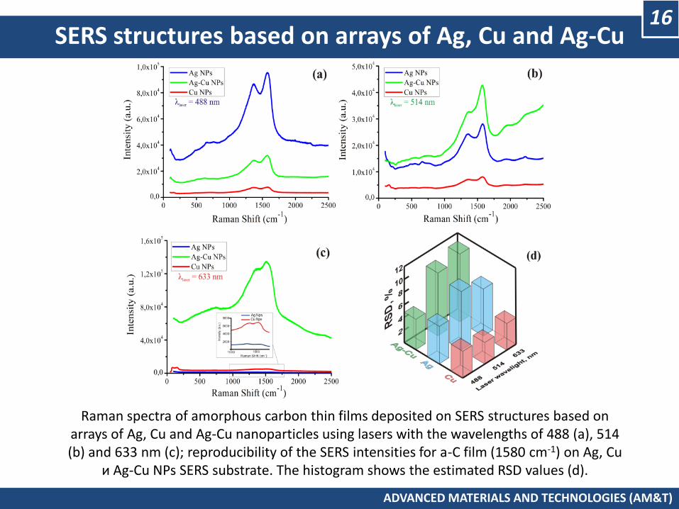
SERS structures based on arrays of Ag, Cu and Ag-Cu
ADVANCED MATERIALS AND TECHNOLOGIES (AM&T)
16
Raman spectra of amorphous carbon thin films deposited on SERS structures based on arrays of Ag, Cu and Ag-Cu nanoparticles using lasers with the wavelengths of 488 (a), 514 (b) and 633 nm (c); reproducibility of the SERS intensities for a-C film (1580 cm-1) on Ag, Cu
и Ag-Cu NPs SERS substrate. The histogram shows the estimated RSD values (d).

Historical Note
Detection of μM Trimethylamine N-oxide
ADVANCED MATERIALS AND TECHNOLOGIES (AM&T)
17
Raman spectra of 0.5 μM, 0.5 mM and 0.5 M of TMAO at wavelength of 514 nm on the structure of Si \Ag\SiO2\Ag
Scheme of TMAO formation in the body
SERS SchemeSERS substrate lifetime

Detection of TMAO in human blood and plasma
ADVANCED MATERIALS AND TECHNOLOGIES (AM&T)
18
Comparison of the literature peaks of TMAO and the corresponding experimental peaks
Raman spectra of human blood and plasma at wavelength of 514 nm on the structure of Si \Ag\SiO2\Ag
band
type
Munro
e et al.
TMA
O μM
TMAO
mM
TMAO
MPlasma Blood
CH3
torsion225 220 220 -
220 219
CH3
torsion293 295 295 -
300 296
CNC
bend386 - - 390
400
N-O
stretch489 480 465 490
487 490
C-N
stretch764 755 760 760
760 750
N-O
stretch945 930 960 950
- -
C-N
stretch945 930 960 950
- -
CH3
def1000 1005 1010 -
1005 996
CH3
rock1136 1130 1155 -
1150 1126
CH3
rock
1231-
12681280 1250 1270
1250 1226
CH3
def
1400-
14651430 1460 1450
1450 1467
C-H
stretch
2931-
29522930 2930 2955
2935 2927
C-H
stretch3036 3060 - 3040
3066 3060

Historical NotePhotosynthesis
ADVANCED MATERIALS AND TECHNOLOGIES (AM&T)
19
СO2 + 3H2 = CH3OH + H2OСO2 + H2 = СО + H2OСО + 2H2 = CH3OH
The use of plasmonic nanoparticles in the composition of the catalyst may allow the use of "free" solar energy for:- Water purification- Processing of co2 into methanol, methane-Decomposition of water into oxygen and hydrogen- Decomposition of exhaust gases of an internal combustion engine

Historical NoteCatalytic systems
ADVANCED MATERIALS AND TECHNOLOGIES (AM&T)
20
TiO2+Au(NPs) TiO2+MWCNT+Au(NPs)
MWCNT+Ag(NPs)
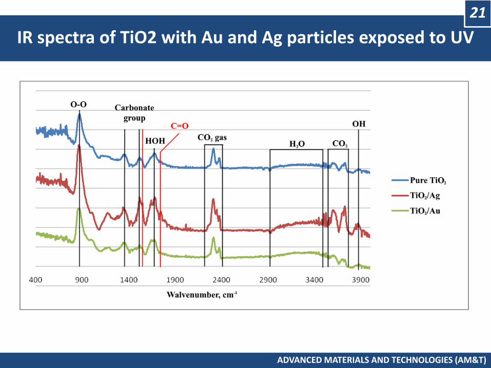
Historical NoteIR spectra of TiO2 with Au and Ag particles exposed to UV
ADVANCED MATERIALS AND TECHNOLOGIES (AM&T)
21

Historical NoteThe photocatalytic activity of TiO2-based catalyst
ADVANCED MATERIALS AND TECHNOLOGIES (AM&T)
22
0
0,05
0,1
0,15
0,2
0,25
0,3
0,35
Me
OH
Yie
ld *
µm
ol/
g*h
+

Historical NoteArticles used for presentation
ADVANCED MATERIALS AND TECHNOLOGIES (AM&T)
23
[1] S.V. Dubkov, A.I. Savitskiy, A.Y. Trifonov, G.S. Yeritsyan, Y.P. Shaman, E.P. Kitsyuk, A. Tarasov, O. Shtyka, R. Ciesielski, D.G. Gromov, SERS in red spectrum region through array of Ag–Cu composite nanoparticles formed by vacuum-thermal evaporation, Optical Materials: X. 7 (2020). https://doi.org/10.1016/j.omx.2020.100055. (IF=2.77, Q1)
[2] S. Dubkov, D. Gromov, A. Savitskiy, A. Trifonov, S. Gavrilov, Alloying effects at bicomponent Au-Cu and In-Sn particle arrays formation by vacuum-thermal evaporation, Materials Research Bulletin. 112 (2019) 438–444. https://doi.org/10.1016/j.materresbull.2018.10.003. (IF=4.019, Q1)
[3] D.G. Gromov, S.V. Dubkov, A.I. Savitskiy, Y.P. Shaman, A.A. Polokhin, I.A. Belogorokhov, A.Y. Trifonov, Optimization of nanostructures based on Au, Ag, Au[sbnd]Ag nanoparticles formed by thermal evaporation in vacuum for SERS applications, Applied Surface Science. 489 (2019) 701–707. https://doi.org/10.1016/j.apsusc.2019.05.286. (IF=6.182, Q1)
[4] O. Shtyka, R. Ciesielski, A. Kedziora, W. Maniukiewicz, S. Dubkov, D. Gromov, T. Maniecki, Photocatalytic Reduction of CO2 Over Me (Pt, Pd, Ni, Cu)/TiO2 Catalysts, Topics in Catalysis. 63 (2020) 113–120. https://doi.org/10.1007/s11244-020-01241-y. (IF=2.406, Q1)
This work was financially supported by the grant of President of the Russian Federation(project MK-2222.2019.8) and by the Russian Science Foundation (Project No. 19-19-00595)

Thanks For Your Attention
ME IN
ADVANCED MATERIALS AND TECHNOLOGIES (AM&T)