monolithic linear ic la4440 - bucek.name · stereo 2 to 8 Ω bridge 4 to 8 Ω ... (g) in case of...
TRANSCRIPT

Any and all SANYO products described or contained herein do not have specifications that can handleapplications that require extremely high levels of reliability, such as life-support systems, aircraft’scontrol systems, or other applications whose failure can be reasonably expected to result in seriousphysical and/or material damage. Consult with your SANYO representative nearest you before usingany SANYO products described or contained herein in such applications.
SANYO assumes no responsibility for equipment failures that result from using products at values thatexceed, even momentarily, rated values (such as maximum ratings, operating condition ranges,or otherparameters) listed in products specifications of any and all SANYO products described or containedherein.
Monolithic Linear IC
6W 2-Channel, Bridge 19W typ Power Amplifier
Ordering number:ENN750F
LA4440
SANYO Electric Co.,Ltd. Semiconductor CompanyTOKYO OFFICE Tokyo Bldg., 1-10, 1 Chome, Ueno, Taito-ku, TOKYO, 110-8534 JAPAN
21500TH (KT)/90196RM/33194HO/8064KI/3233KI/O070KI, TS No.750–1/13
Package Dimensionsunit:mm
3023A-SIP14H
[LA4440]
SANYO : SIP14H
Features• Built-in 2 channels (dual) enabling use in stereo and bridge
amplifier applications.Dual : 6W×2 (typ.)Bridge : 19W (typ.)
• Minimun number of external parts required.• Small pop noise at the time of power supply ON/OFF and
good starting balance.• Good ripple rejection : 46dB (typ.)• Good channel separation.• Small residual noise (Rg=0).• Low distortion over a wide range from low frequencies to
high frequencies.• Easy to design radiator fin.• Built-in audio muting function.• Built-in protectors.
a. Thermal protectorb. Overvoltage, surge voltage protectorc. Pin-to-pin short protector
SpecificationsAbsolute Maximum Ratings at Ta = 25˚C
˚C
˚C
141
13.8
0.6
37.0
30.0
R1.
7
11.0
8.0
0.8m
in
6.0
15.0
max
1.99 2.54 1.40.4
4.5
2.25
retemaraP lobmyS snoitidnoC sgnitaR tinU
egatlovylppusmumixaMV CC 1xam )s03=t(tnecseiuQ 52 V
V CC 2xam gnitarepO 81 V
egatlovylppusegruS V CC )egrus( t≤ s2.0 05 V
noitapissidrewopelbawollA xamdP 51 W
ecnatsiserlamreT θ c-j esac-ot-noitcnuJ 3
erutarepmetgnitarepO rpoT 57+ot02–
erutarepmetegarotS gtsT 051+ot04–
˚C/W
Recommended Operating Conditions at Ta = 25˚C
Tc=75˚C, See Pd max – Ta characteristic
retemaraP lobmyS snoitidnoC sgnitaR tinU
egatlovylppuS V CC 2.31 V
ecnatsiserdaoL RLoeretS 8ot2 Ω
egdirB 8ot4 Ω

LA4440
No.750–2/13
Operating Characteristics at Ta = 25˚C, VCC=13.2V, RL=4Ω, f=1kHz, Rg=600Ω, with 100×100×1.5mm3 Al fin,
See specified Test Circuit.
retemaraP lobmyS snoitidnoCsgnitaR
tinUnim pyt xam
tnerructnecseiuQ occI 001 002 Am
niagegatloV GV 5.94 5.15 5.35 Bd
rewoptuptuO POoeretS,%01=DHT 0.5 0.6 W
egdirB,%01=DHT 91 W
noitrotsidcinomrahlatoT DHT PO W1= 1.0 0.1 %
ecnatsisertupnI ri k03 Ω
egatlovesiontuptuO V ON0=gR 6.0 0.1 Vm
k01=gR Ω 0.1 0.2 Vm
oitarnoitcejerelppiR Rr VR f,Vm002= R 0=gR,zH001= 64 Bd
noitarapeslennahC peshC VO k01=gR,mBd0= Ω 54 55 Bd
noitaunettagnituM TTA VO V,mBd0= M V9= 04 Bd
slennahcneewtebecnereffidniaG ∆ GV 2 Bd
Equivalent Circuit Block Diagram

LA4440
No.750–3/13
Sample Application Circuit 1. Stereo use
Sample Application Circuit 2. Bridge amplifier 1

LA4440
No.750–4/13
Sample Application Circuit 3. Bridge amplifier 2
Description of External PartsC1 (C2) · Feedback capacitor : The low cutoff frequency depends on this capacitor.
If the capacitance value is increased, the starting time is delayed.C3 (C4) · Bootstrap capacitor : If the capacitance value is decreased, the output at low frequencies goes lower.C5 (C6) · Oscillation preventing capacitor : Polyester film capacitor, being good in temperature characteristic,
frequency characteristic, is used.The capacitance value can be reduced to 0.047µF depending on the stability of the board.
C7 (C8) · Output capacitor : The low cutoff frequency depends on this capacitor.At the bridge amplifier mode, the output capacitor is generally connected.
C9 · Decoupling capacitor :Used for the ripple filter. Since the rejection effect is saturated at a certaincapacitance value, it is meaningless to increase the capacitance value more than required. This capaci-tor, being also used for the time constant of the muting circuit, affects the starting time.
R1 (R2) · Filter resistor for preventing oscillation.R3 (R4) · Resistor for making input signal of inverting amplifier in Voltage Gain Adjust at Bridge Amplifier
Mode (No. 1).R5 · Resistor for adjusting starting time in Voltage Gain Adjust at Bridge Amplifier Mode (No. 2)C10 · Capacitor for preventing oscillation in Voltage Gain Adjust at Bridge Amplifier Mode (No. 2)C11 · Power source capacitor.R6 (R7) · Used at bridge amplifier mode in order to increase discharge speed and to secure transient stability.
Feaures of IC System and Functions of Remaining Pins(a) Since the input circuit uses PNP transistors and the input potential is designed to be 0 bias, no input coupling
capacitor is required and direct coupling is available. However, when slider contact noise caused by the variableresistor presents a problem, connect an capacitor in series with the input.
(b) The open-loop voltage gain is lowered and the negative feedback amount is reduced for stabilization. An increasein distortion resulted from the reduced negative feedback amount is avoided by use of the built-in unique distor-tion reduction circuit, and thus distortion is kept at 0.1% (typ.).
(c) A capacitor for oscillation compensation is contained as a means of reducing the number of external parts. Thecapacitance value is 35pF which determines high cutoff frequency fH (–3dB point) of the amplifier (fH≈20kHz).
(d) For preventing the IC from being damaged by a surge applied on the power line, an overvoltage protector iscontained. Overvoltage setting is 25V. It is capable of withstanding up to 50V at giant pulse surge 200ms.
(e) No damege occurs even when power is applied at a state where pins 10, 11, and 12 are short-circuited with solderbridge, etc.
(f) To minimize the variations in voltage gain, feedback resistor RNF is contained and voltage gain (51.5dB) is fixed.
LA4440
No.750–5/13
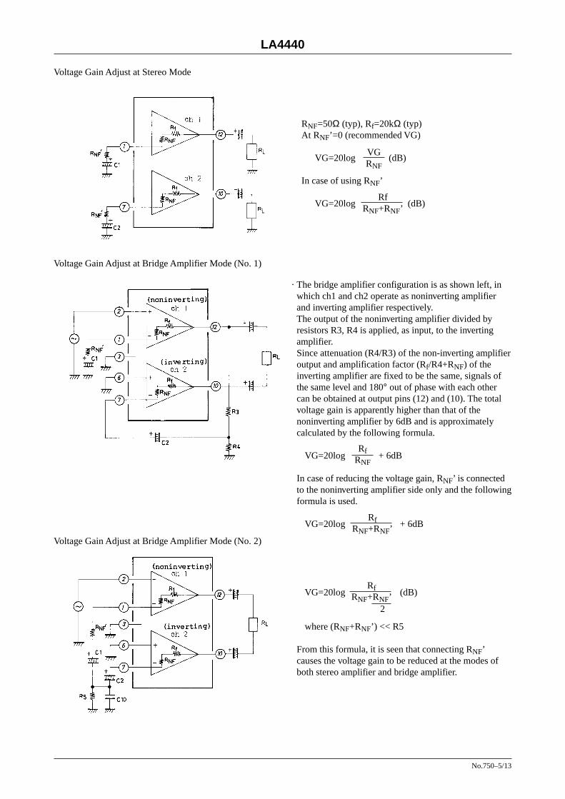
Voltage Gain Adjust at Stereo Mode
RNF=50Ω (typ), Rf=20kΩ (typ)At RNF’=0 (recommended VG)
VG=20log (dB)
In case of using RNF’
VG=20log (dB)
VGRNF
RfRNF+RNF’
Voltage Gain Adjust at Bridge Amplifier Mode (No. 1)
· The bridge amplifier configuration is as shown left, inwhich ch1 and ch2 operate as noninverting amplifierand inverting amplifier respectively.The output of the noninverting amplifier divided byresistors R3, R4 is applied, as input, to the invertingamplifier.Since attenuation (R4/R3) of the non-inverting amplifieroutput and amplification factor (Rf/R4+RNF) of theinverting amplifier are fixed to be the same, signals ofthe same level and 180° out of phase with each othercan be obtained at output pins (12) and (10). The totalvoltage gain is apparently higher than that of thenoninverting amplifier by 6dB and is approximatelycalculated by the following formula.
VG=20log + 6dB
In case of reducing the voltage gain, RNF’ is connectedto the noninverting amplifier side only and the followingformula is used.
VG=20log + 6dB
VG=20log (dB)
where (RNF+RNF’) << R5
From this formula, it is seen that connecting RNF’causes the voltage gain to be reduced at the modes ofboth stereo amplifier and bridge amplifier.
RfRNF
Voltage Gain Adjust at Bridge Amplifier Mode (No. 2)
RfRNF+RNF’
RfRNF+RNF’
2

LA4440
No.750–6/13
(g) In case of applying audio muting in each application circuit, the following circuit is used.
6V≤VM≤VCCRecommended VM=9VATT=40dB (Rg=600Ω)
Flow-in current IO is calculated by the following formula.
IO=
In case of increasing the muting attenuation, resistor 5.6kΩ is connected in series with the input, and then theattenuation is made to be 55dB. Be careful that connecting an input capacitor causes pop noise to be increased atthe time of application of AC muting. Increased RO, CO make it possible to reduce the noise. In case of com-pletely cutting off power IC, pin (5) is grounded, and then DC control is available and the attenuation is made tobe ∞.
VM – VBERO
Stereo : 20Ω≤R≤100ΩBridge No.1 : 20Ω≤R≤100ΩBridge No. 2 : 0Ω≤R≤50Ω
Pin Voltage (unit : V)
.oNniP 1 2 3 4 5 6 7 8 9 01 11 21 31 41
nipnoitcnuF 1HCFN
1HCFN
erPDNG
CAoiduAgnituM
CD 2HCNI
2HCFN
2HCrewoP
DNG
2HCSB
2HCTUO V CC
1HCTUO
1HCSB
1HCrewoP
DNG
taegatloVniPedomtnecseiuq 4.1 30.0 0 0 0.31 30.0 4.1 0 9.11 8.6 2.31 8.6 9.11 0
Proper Cares in Using IC· Maximum ratingsIf the IC is used in the vicinity of the maximum ratings, even a slight variation in conditions may cause the maximumratings to be exceeded, thereby leading to breakdown. Allow an ample margin of variation for supply voltage, etc. anduse the IC in the range where the maximum ratings are not exceeded.
· Printed circuit boardWhen making the board, refer to the sample printed circuit pattern and be careful that no feedback loop is formedbetween input and output.
· Oscillation preventing capacitorNormally, a polyester film capacitor is used for 0.1µF + 4.7Ω. The capacitance value can be reduced to 0.047µF depend-ing on the stability of the board.
· OthersConnect the radiator fin of the package to GND.

LA4440
No.750–7/13
Characteristics at stereo amplifier mode

LA4440
No.750–8/13

LA4440
No.750–9/13
Characteristics at bridge amplifier mode No. 1

LA4440
No.750–10/13

LA4440
No.750–11/13
Characteristics at bridge amplifier mode No. 2

LA4440
No.750–12/13
Proper Cares in Mounging Radiator Fin1. The mounting torque is in the range of 39 to 59N · cm.2. The distance between screw holes of the radiator fin must coincide with the distance between screw holes of the IC.
With case outline dimensions L and R referred to, the screws must be tightened with the distance between them asclose to each other as possible.
3. The screw to be used must have a head equivalent to the one of truss machine screw or binder machine screw definedby JIS. Washers must be also used to protect the IC case.
4. No foreign matter such as cutting particles shall exist between heat sink and radiator fin. When applying grease on thejunction surface, it must be applied uniformly on the whole surface.
5. IC lead pins are soldered to the printed circuit board after the radiator fin is mounted on the IC.

Specifications of any and all SANYO products described or contained herein stipulate the performance, characteristics, and functions of the described products in the independent state, and are not guaranteesof the performance, characteristics, and functions of the described products as mounted in the customer'sproducts or equipment. To verify symptoms and states that cannot be evaluated in an independent device, the customer should always evaluate and test devices mounted in the customer's products or equipment.
SANYO Electric Co., Ltd. strives to supply high-quality high-reliability products. However, any and allsemiconductor products fail with some probability. It is possible that these probabilistic failures could give rise to accidents or events that could endanger human lives, that could give rise to smoke or fire,or that could cause damage to other property. When designing equipment, adopt safety measures sothat these kinds of accidents or events cannot occur. Such measures include but are not limited to protectivecircuits and error prevention circuits for safe design, redundant design, and structural design.
In the event that any or al l SANYO products(including technical data,services) described or contained herein are controlled under any of applicable local export control laws and regulations,such products must not be expor ted without obtaining the expor t l icense from the authorit iesconcerned in accordance with the above law.
No part of this publication may be reproduced or transmitted in any form or by any means, electronic ormechanical, including photocopying and recording, or any information storage or retrieval system,or otherwise, without the prior written permission of SANYO Electric Co. , Ltd.
Any and all information described or contained herein are subject to change without notice due toproduct/technology improvement, etc. When designing equipment, refer to the "Delivery Specification"for the SANYO product that you intend to use.
Information (including circuit diagrams and circuit parameters) herein is for example only ; it is notguaranteed for volume production. SANYO believes information herein is accurate and reliable, butno guarantees are made or implied regarding its use or any infringements of intellectual property rightsor other rights of third parties.
This catalog provides information as of February, 2000. Specifications and information herein are subject
to change without notice.
LA4440
PS No.750–13/13