mosfet operation
DESCRIPTION
MOSFET operation. Animation of the MOSFET manufacturing process I encourage you to look at the website given below and use the button “animate to next” – the actual process is described for each step. http://jas.eng.buffalo.edu/education/fab/NMOS/nmos.html. Basic structure of the MOSFET. - PowerPoint PPT PresentationTRANSCRIPT


Animation of the MOSFET manufacturing process
I encourage you to look at the website given below and use the button
“animate to next” – the actual process is described for each step.
http://jas.eng.buffalo.edu/education/fab/NMOS/nmos.html
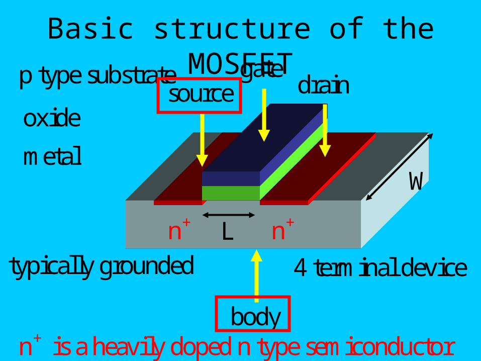
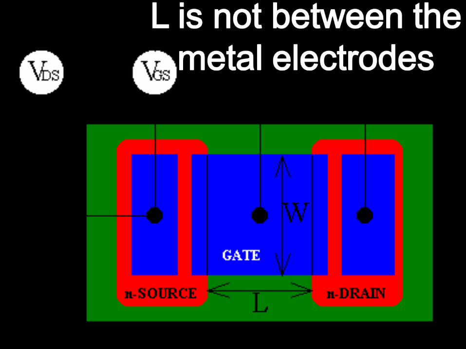
Basic structure of the MOSFETp type substrate
W
oxide
L
metal
+n
source draingate
+n
+n is a heavily doped n type semiconductorbody
4 terminal devicetypically grounded
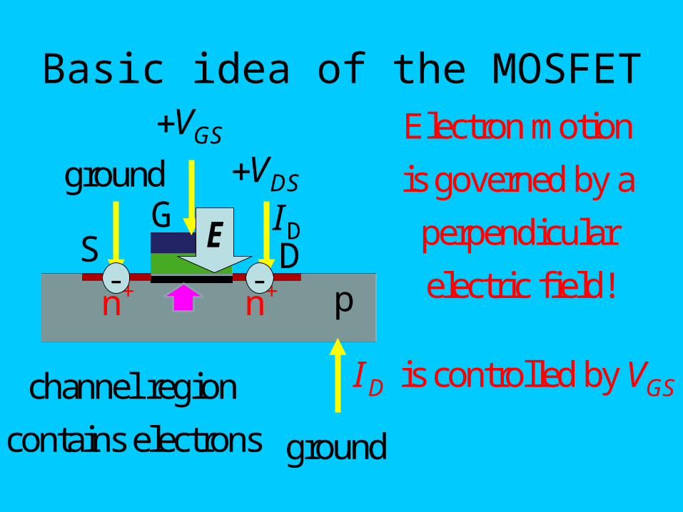
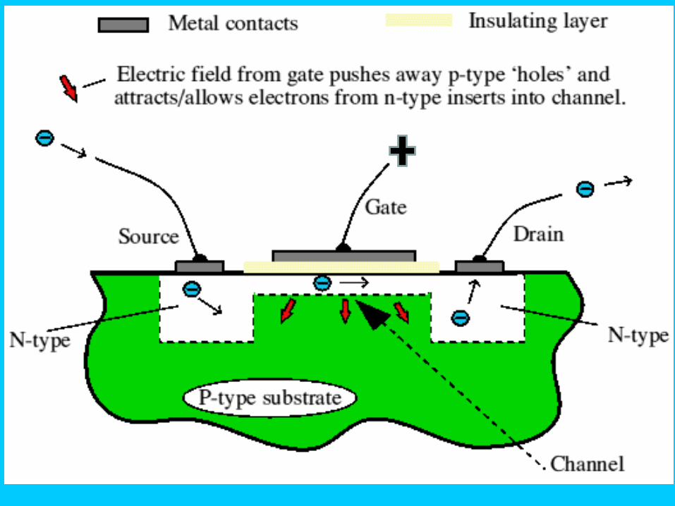
Basic idea of the MOSFET
p+n
S DG
+n
GSV
DI
channel region
contains electrons
DSV
ground
ground
- -
E
Electron motion
is governed by a
perpendicular
electric field!
is controlled by D GSI V
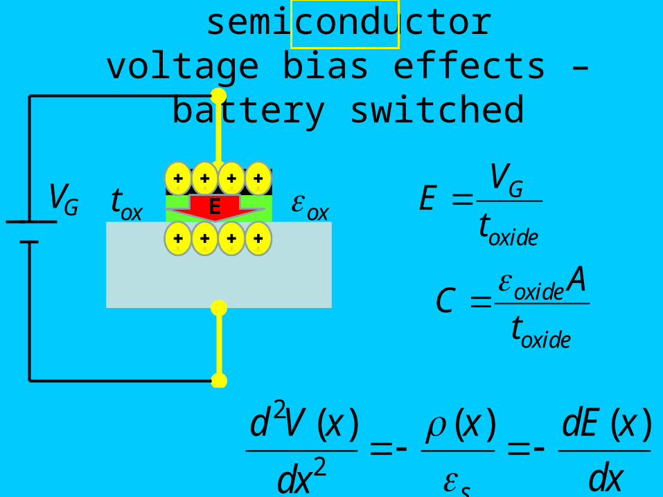
MOS capacitor p type semiconductorvoltage bias effects –battery switched
oxide
oxide
AC
t
G
oxide
VE
toxt oxGV E
2
2
( ) ( ) ( )
s
d V x x dE x
dxdx
GV
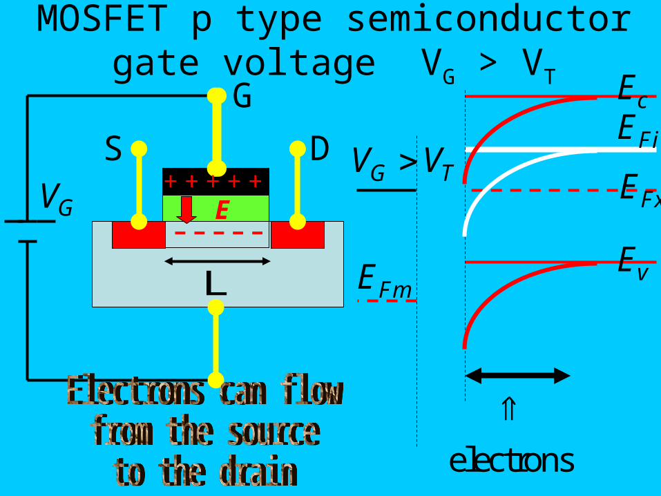
MOSFET p type semiconductor gate voltage VG > VT
cE
vE
FxE
FiE
FmE
G TV V
electrons
- - - - -
+ + + + +E
G
DS
L
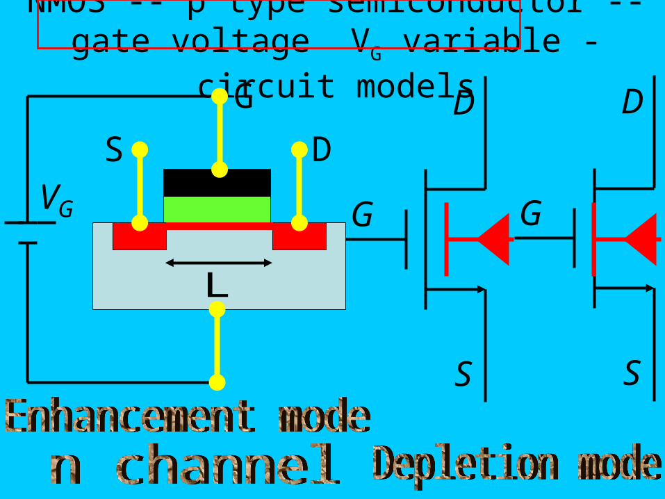
NMOS -- p type semiconductor -- gate voltage VG variable - circuit models
GV
S
G
DD
S
G
D
S
G
L
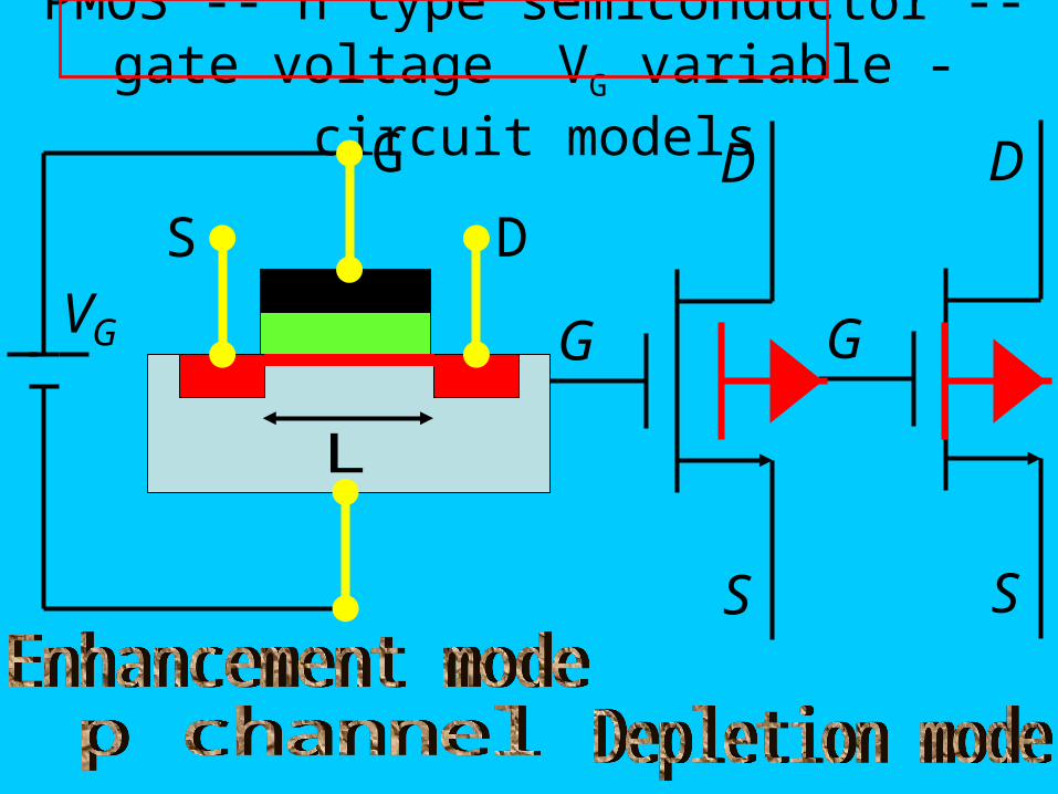
PMOS -- n type semiconductor -- gate voltage VG variable - circuit models
GV
S
G
DD
S
G
D
S
G
L
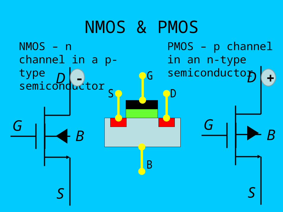
NMOS & PMOSNMOS – n channel in a p-type semiconductor
PMOS – p channel in an n-type semiconductor
D
S
GB
D
S
GB
S
G
D
B
- +
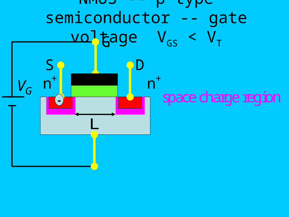
NMOS -- p type semiconductor -- gate voltage VGS < VT
GV
G
S D+n+nspace charge region-
L
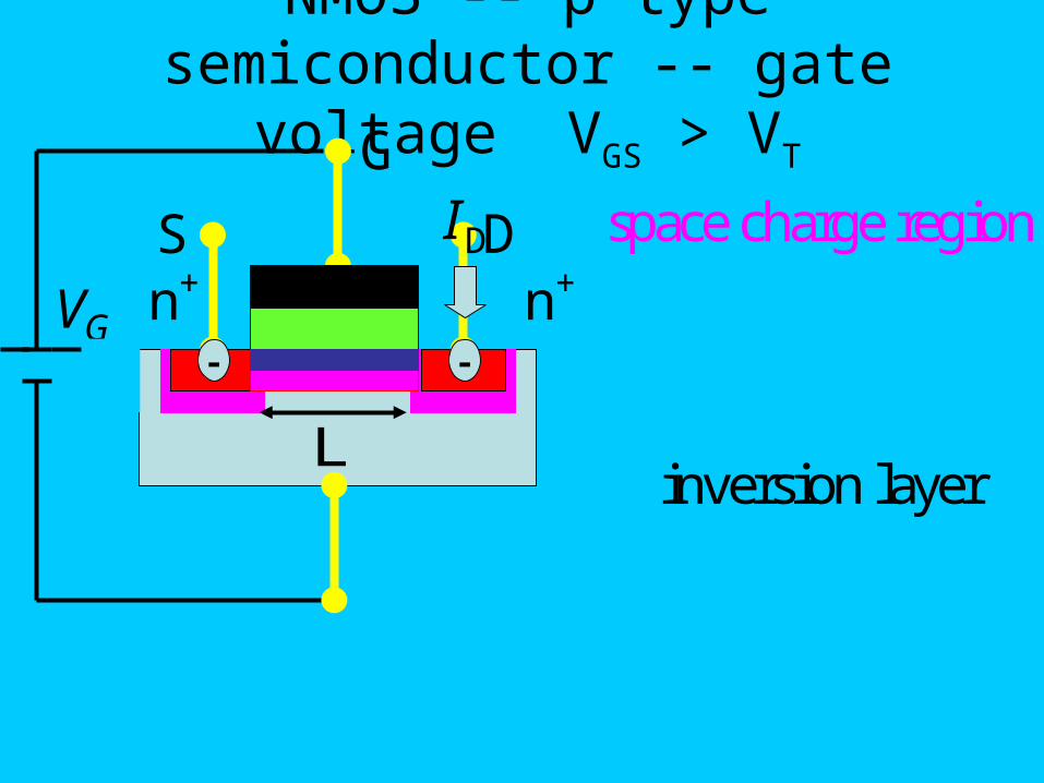
NMOS -- p type semiconductor -- gate voltage VGS > VT
space charge region
GV
G
S D+n+n
inversion layer
--
DI
L
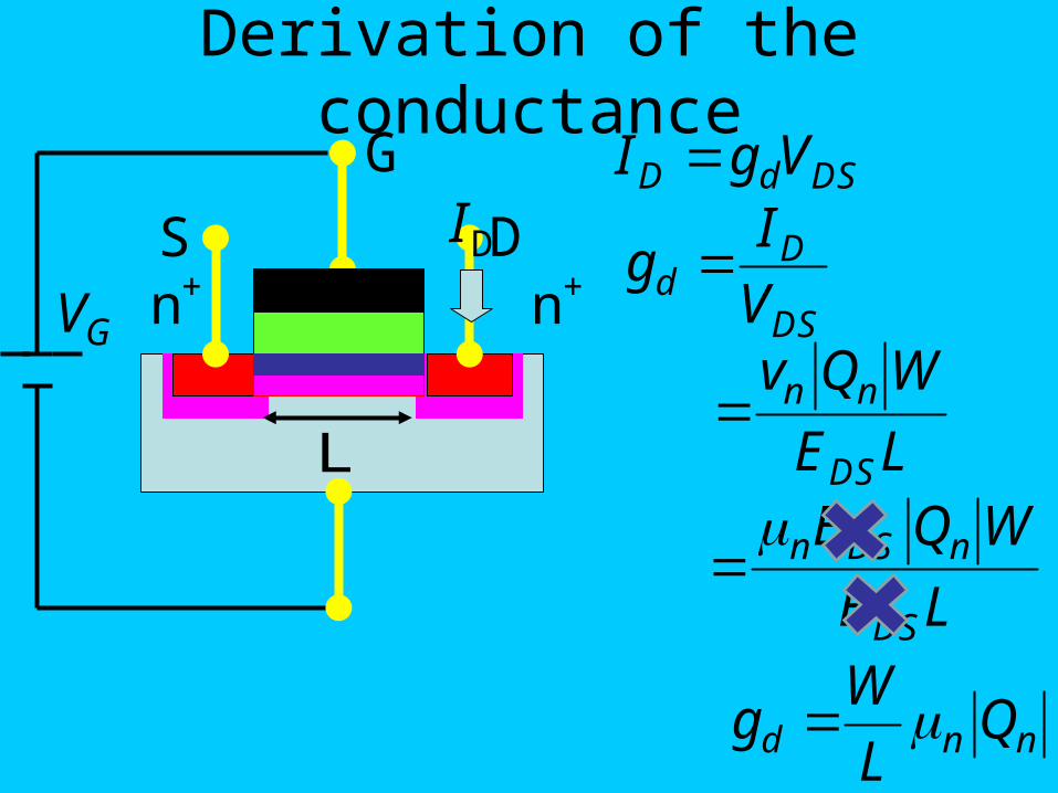
D d DSI g V
d n nW
g QL
Derivation of the conductance
Dd
DS
Ig
V
n n
DS
v Q W
E L
n DS n
DS
E Q W
E L
GV
G
S D+n+n
DI
L
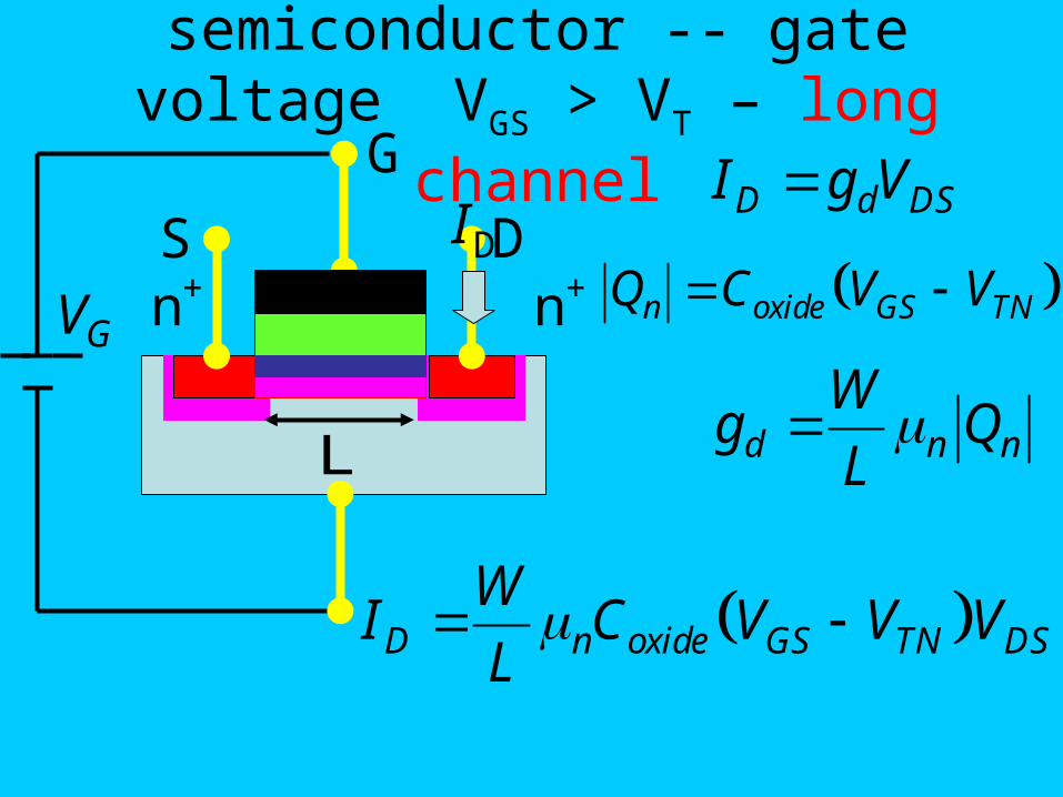
NMOS -- p type semiconductor -- gate voltage VGS > VT – long channel
GV
G
S D+n+n
D d DSI g VDI
d n nW
g QL
n oxide GS TNQ C V V
D n oxide GS TN DSW
I C V V VL
L
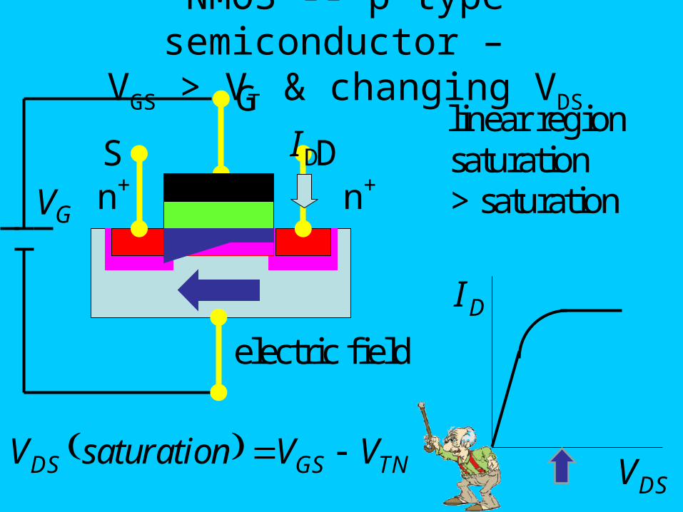
NMOS -- p type semiconductor – VGS > VT & changing VDS
GV
G
S D+n+n
linear regionDI saturation
> saturation
DI
DSV
DS GS TNV saturation V V
electric field
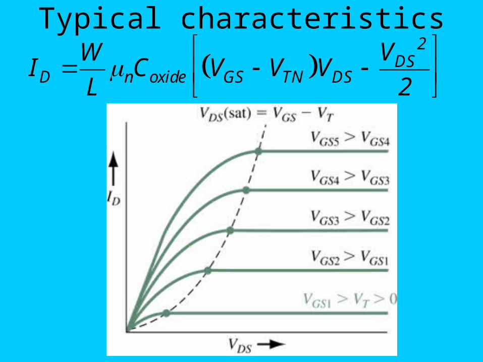
Typical characteristics
2
DSD n oxide GS TN DS
VWI C V V V
L 2
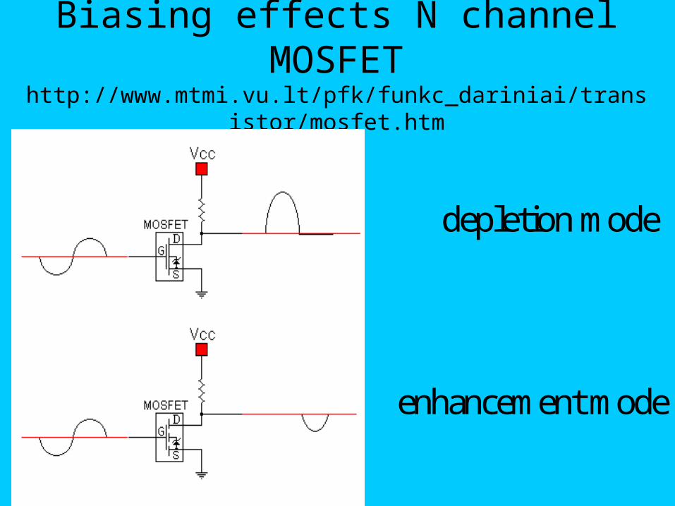
Biasing effects N channel MOSFEThttp://www.mtmi.vu.lt/pfk/funkc_dariniai/transistor/mosfet.htm
depletion mode
enhancement mode


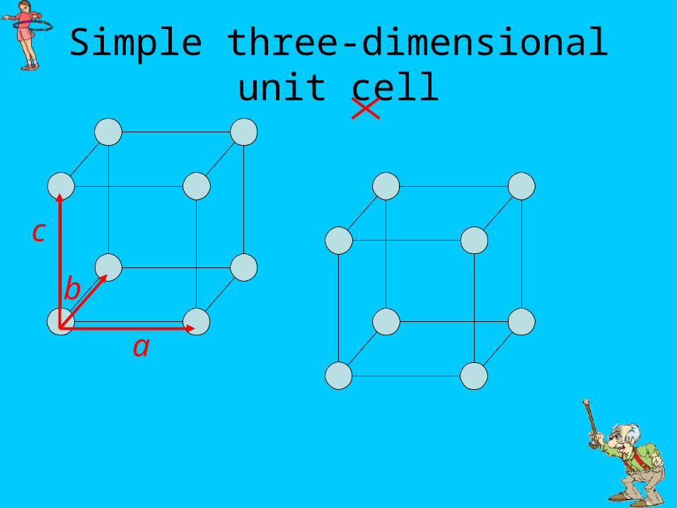
Simple three-dimensional unit cell
a
b
c