motor control shield with btn8982ta for arduino user manual
TRANSCRIPT

User Manual Revision 1.0
www.infineon.com 2016-06-30
Motor Control Shield for Arduino
Motor Control Shield with BTN8982TA for Arduino
About this document
Scope and purpose
This document describes how to use the Motor Control Shield with BTN8982TA for Arduino.
Intended audience
Engineers, hobbyists and students who want to add a powerful Motor Control to Arduino projects.
Related information
Table 1 Supplementary links and document references
Reference Description
BTN8982TA Reference Manuals Product page which contains reference information for the half-bridge BTN8982TA
Arduino Home Page All information on Arduino
Arduino Uno Product Page Arduino Uno R3 description
DAVE™ Development Platform All details on DAVE™ IDE
XMC1100 Boot Kit Product page which contains reference information
for the XMC1100 Boot Kit

User Manual 2 Revision 1.0
2016-06-30
Motor Control Shield with BTN8982TA For Arduino
Table of Contents
About this document ....................................................................................................................... 1
Table of Contents ........................................................................................................................... 2
1 Motor Control Shield introduction ................................................................................... 3
1.1 Motor Control Shield overview ............................................................................................................... 3 1.2 Key features ............................................................................................................................................. 3 1.3 Blockdiagram of a bi-directional Motor Control .................................................................................... 5
2 Motor Control Shield board description ........................................................................... 6
2.1 Schematics .............................................................................................................................................. 6 2.2 Layout ...................................................................................................................................................... 7 2.3 Important design and layout rules ......................................................................................................... 8
2.4 Pin assignment ........................................................................................................................................ 9 2.5 Pin definitions and functions ................................................................................................................ 10
3 BTN8982TA overview .................................................................................................... 11 3.1 Key features of the BTN8982TA Novalith IC™ ....................................................................................... 11
3.2 Block diagram ....................................................................................................................................... 12 3.3 Pin assignment ...................................................................................................................................... 13
3.4 13 3.5 Pin definitions and functions BTN8982TA ............................................................................................ 13
4 Getting started ............................................................................................................. 14 4.1 Target applications ............................................................................................................................... 14
4.2 Typical target application ..................................................................................................................... 14
4.2.1 Getting started: Shield ..................................................................................................................... 14
4.2.2 Getting started: Software ................................................................................................................ 15 4.2.3 Software hints .................................................................................................................................. 18
Revision History ............................................................................................................................ 20
No table of figures entries found.
User Manual 3 Revision 1.0
2016-06-30
Motor Control Shield with BTN8982TA For Arduino
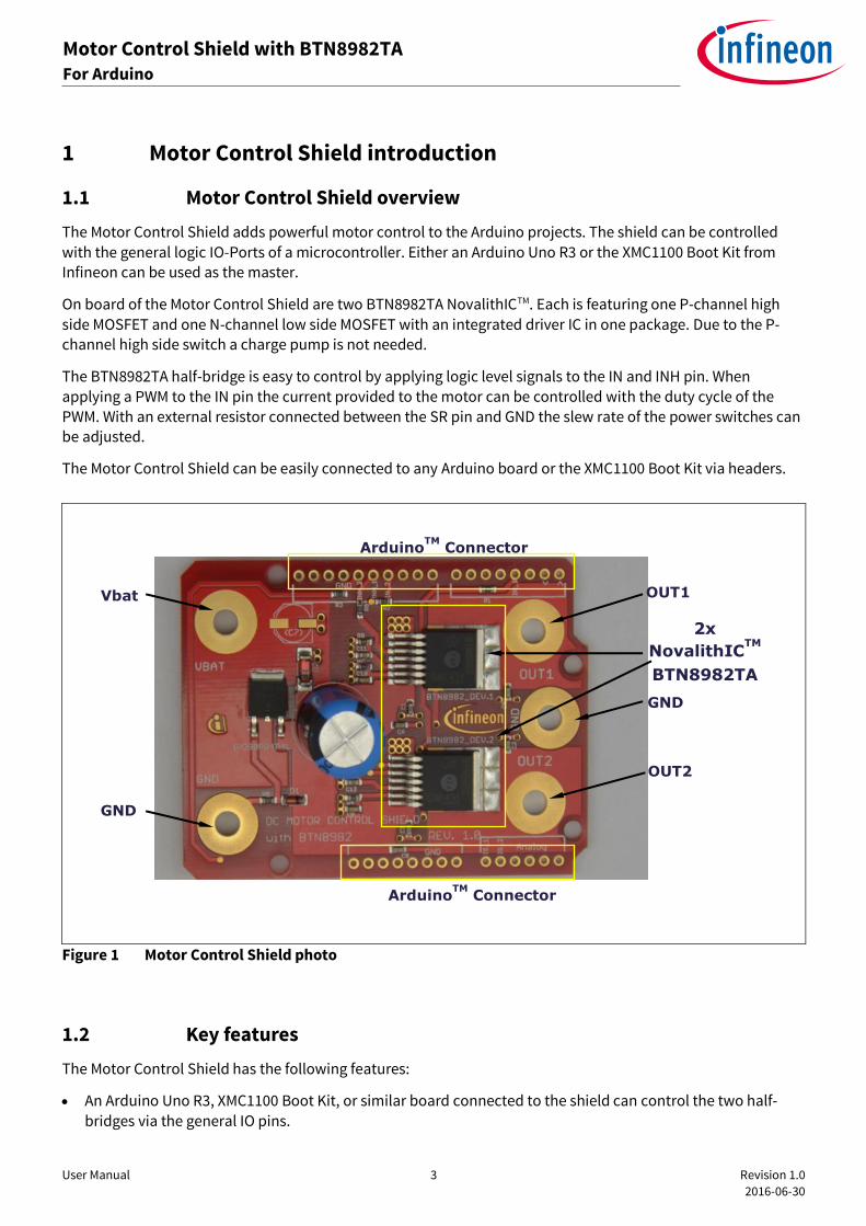
1 Motor Control Shield introduction
1.1 Motor Control Shield overview
The Motor Control Shield adds powerful motor control to the Arduino projects. The shield can be controlled
with the general logic IO-Ports of a microcontroller. Either an Arduino Uno R3 or the XMC1100 Boot Kit from Infineon can be used as the master.
On board of the Motor Control Shield are two BTN8982TA NovalithICTM. Each is featuring one P-channel high
side MOSFET and one N-channel low side MOSFET with an integrated driver IC in one package. Due to the P-channel high side switch a charge pump is not needed.
The BTN8982TA half-bridge is easy to control by applying logic level signals to the IN and INH pin. When
applying a PWM to the IN pin the current provided to the motor can be controlled with the duty cycle of the PWM. With an external resistor connected between the SR pin and GND the slew rate of the power switches can be adjusted.
The Motor Control Shield can be easily connected to any Arduino board or the XMC1100 Boot Kit via headers.
Figure 1 Motor Control Shield photo
1.2 Key features
The Motor Control Shield has the following features:
An Arduino Uno R3, XMC1100 Boot Kit, or similar board connected to the shield can control the two half-
bridges via the general IO pins.
Vbat
GND
OUT1
2x
NovalithICTM
BTN8982TA
GND
ArduinoTM
Connector
OUT2
ArduinoTM
Connector

User Manual 4 Revision 1.0
2016-06-30
Motor Control Shield with BTN8982TA For Arduino
Brushed DC Motor Control up to 250 W continuous load
o 8 – 18 V nominal input voltage (max. 6 – 40 V)
o Average motor current 30 A restricted due to the limited power dissipation of the PCB (BTN8982TA current limitation @ 55 A min.)
Drives either one brushed bi-directional DC motor or two uni-directional DC motors.
Capable of high frequency PWM, e.g. 30 kHz
Adjustable slew rates for optimized EMI by changing external resistor
Driver circuit with logic level inputs
Status flag diagnosis with current sense capability
Protection e.g. against overtemperature and overcurrent
Reverse polarity protection with IPD90P04P4L
Further comments:
o To keep the costs as low as possible the pin headers and connectors are not attached to the
shield. The user can solder them by himself. The pin headers are not expensive, but the through whole soldering is a not insignificant cost factor.
o The size of the DC-link capacity (C4 in the schematics and C10 in the application circuit.) with 1000µF is for most applications oversized. It is a worst case scenario if a 500W motor is
connected to the shield. The capacity can be replaced by smaller capacities when using less powerful motors. As described in the chapter “4.2.1 Calculation of the DC-link capacitor and Pi-
filter”, equation 4.9 in the BTN8960 /62 /80 /82 High Current PN Half Bridge NovalithICTM
Application Note (Rev. 0.4, 2015-07-02) should be used to calculate the value of the DC-link
capacity.
Figure 2 Motor Control Shield driving an engine cooling fan

User Manual 5 Revision 1.0
2016-06-30
Motor Control Shield with BTN8982TA For Arduino
1.3 Blockdiagram of a bi-directional Motor Control
As a starting point for the Motor Control Shield, the application block diagram shown in Figure 3 was used. For
simplicity reasons the conductivity L1 was removed in the Shield schematics. In the application block diagram the INH pins of both half-bridges are connected to one IO-port of the microcontroller. To be more flexible in the usage of the Motor Control Shield each INH of the two half-bridges is connected to a separate IO pin.
Figure 3 Application circuit for a bi-directional motor control with BTN8982TA
optional
M
XC866 TLE
4278G
I/O
Reset
Vdd
Vss
WO
RO
Q
D GND
I
Microcontroller Voltage Regulator
C19
100nF
CD
47nF
CQ
22µF
C10
1000µFR11
10k
R12
10k
R111
0..51k
R112
1k
I/OI/O
CI
470nF
C1O2V
220nF
C1OUT
220nF
C2O2V
220nF
C2OUT
220nF
C29
100nF
R211
0..51k
I/OA/D
R22
10k
R21
10k
R212
1k
A/D
INH
IN
IS
SR
BTN8982TA
VS
OUT
GND
INH
IN
IS
SR
BTN8982TA
VS
OUT
GND
VS
Reverse Polarity
Protection
(IPD90P03P4L-04)
R3
10k
DZ1
10V
C1
100nF
L1
C22
100nF
C2IS
1nF
C1IS
1nF
C12
100nF

User Manual 6 Revision 1.0
2016-06-30
Motor Control Shield with BTN8982TA For Arduino
2 Motor Control Shield board description
For a safe and sufficient motor control design, discrete components are needed. Some of them must be dedicated to the motor application and some to the NovalithIC™.
Figure 4, Figure 5 and Figure 6 show the schematics plus the corresponding layout of the Motor Control Shield.
Due to the possibility of using the Shield with loads which can draw a current of up to 55 A the connectors Vbat, GND, OUT1 and OUT2 are designed as solid 4mm through whole connectors. This provides the possibility to
connect plugs which are capable of such high currents. Nevertheless the thermal performance of the Shield
itself limits the possible current which should be applied to the Motor Control Shield to 30 A. To reach the best performance in terms of parasitic inductance and EMC a GND plane, with maximal size was designed.
2.1 Schematics
In Figure 4 the schematics of the Motor Control Shield is shown. The schematics are based on the application circuit in the BTN8982TA Data Sheet.
Figure 4 Schematics Motor Control Shield for Arduino with BTN8982TA

User Manual 7 Revision 1.0
2016-06-30
Motor Control Shield with BTN8982TA For Arduino
2.2 Layout
Figure 5 and Figure 6 show the layout of the Motor Control Shield. The layout follows the design rules in the BTN8960 /62 /80 /82 High Current PN Half Bridge NovalithICTM Application Note (also see Chapter 2.3).
Figure 5 Motor Control Shield – Bottom and top layers
Figure 6 Motor Control Shield for Arduino with BTN8982TA – Layout

User Manual 8 Revision 1.0
2016-06-30
Motor Control Shield with BTN8982TA For Arduino
Figure 7 Motor Control Shield for Arduino with BTN8982TA – Bill of Material (BOM)
2.3 Important design and layout rules
The basis for the following design and layout recommendations is the parasitic inductance of electrical wires
and design guidelines as described in Chapter three and four of the Application Note BTN8960 /62 /80 /82 High
Current PN Half Bridge NovalithICTM (Rev. 0.4, 2015-07-02).
C4, so called DC-link capacitor: This electrolytic capacitor is required to keep the voltage ripple at the Vs-pin
of the NovalithIC™ low during switching operation (the applied measurement procedure for the supply
voltage is described in Chapter 3.1 of the Application Note). It is strongly recommended that the voltage
ripple at the NovalithIC™ Vs-pin to the GND-pin is kept below 1 V peak to peak. The value of C4 must be aligned accordingly. See therefore Equation (4.9) in the Application Note. Most electrolytic capacitors are less effective at cold temperatures. It must be assured that C4 is also effective under the worst case conditions of the application. The layout is very important too. As shown in Figure 6, the capacitor C4 must
be positioned with very short wiring close to the NovalithIC™. This must be done to keep the parasitic
inductors of the PCB-wires as small as possible.
C1/C3: This ceramic capacitors support C4 to keep the supply voltage ripple low and cover the fast transients between the Vs-pin and the GND-pin. The value of these ceramic capacitors must be chosen so that fast Vs-ripples at the NovalithIC™ do not exceed 1V peak to peak. The layout wiring for C1/C3 must be
shorter than for C4 to the NovalithIC™ to keep the parasitic PCB-wire inductance as small as possible. In

User Manual 9 Revision 1.0
2016-06-30
Motor Control Shield with BTN8982TA For Arduino
addition the parasitic inductance could be kept low by placing at least two vias for the connection to the GND-layer.
C6/C8: These ceramic capacitors are important for EMI in order to avoid entering RF into the NovalithIC™ as much as possible. Good results have been achieved with a value of 220 nF. In terms of layout, it is important
to place these capacitors between “OUT” and “Vs” without significant additional wiring from C6/C8 to the Vs- and OUT-line.
C5/C2: These ceramic capacitor help to improve the EMC immunity and the ESD performance of the application. Good results have been achieved with a value of 220 nF. To keep the EMC and ESD out of the
board, the capacitor is most effective when positioned directly next to the board connector. In addition, the parasitic inductance could be kept low by placing at least two vias for the connection to the GND-layer.
Other components:
IC0, D1 and R8: Reverse polarity protection. See Chapter 4.4 of the Applikation Note.
R9/R6: Slew rate resistors according to data sheet.
C11/C12: Stabilization for slew rate resistors (R9/R6).
R7/R4: Resistors to generate a current sensing voltage from the IS current.
C10/C9: Ceramic capacitors for EMC immunity improvement. GND connection with at least two GND-vias. A
good value is 1nF. In case the current should be measured during the PWM-phase this capacitor must be adapted to the ON-time inside the PWM-phase.
R1, R2, R3 and R5: Device protection in case of microcontroller pins shorted to Vs.
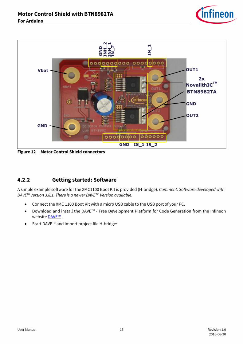
2.4 Pin assignment
To use the Motor Control Shield the necessary control signals can be applied directly at the ArduinoTM
connectors. There is no need to use an Arduino or XMC 1100 Boot Kit to get the Motor Control Shield into an
application. The control pins are logic level inputs which can be driven by any other microcontroller or with
logic level signals. Besides the supply voltage Vbat has to be provided to the Vbat connector. Figure 8 shows the pinout/connectors of the Motor Control Shield.
Figure 8 Motor Control Shield connectors
IN
H_
1
Vbat
GND
OUT1
2x
NovalithICTM
BTN8982TA
GND
OUT2
IS_1
IN
H_
2
IN
_2
IN
_1
IS_2
GND
GN
D

User Manual 10 Revision 1.0
2016-06-30
Motor Control Shield with BTN8982TA For Arduino
2.5 Pin definitions and functions
Pin Symbol I/O Function
GND GND - Ground
D3 IN_1 I Input bridge 1
Defines whether high- or low side switch is activated
D11 IN_2 I Input bridge 2
Defines whether high- or low side switch is activated
D12 INH_1 I Inhibit bridge 1
When set to low device goes in sleep mode
D13 INH_2 I Inhibit bridge 2
When set to low device goes in sleep mode
OUT_1 OUT_1 O Power output of the bridge 1
OUT_2 OUT_2 O Power output of the bridge 2
A0 IS_1 O Current Sense and Diagnostics of half-bridge 1
A1 IS_2 O Current Sense and Diagnostics of half-bridge 2
Vbat Vbat - Supply (Vs after the reverse polarity protection)

User Manual 11 Revision 1.0
2016-06-30
Motor Control Shield with BTN8982TA For Arduino
3 BTN8982TA overview
The BTN8982TA used in the Motor Control Shield is an integrated high current half-bridge for motor drive
applications. It is part of the NovalithIC™ family containing one p-channel high side MOSFET and one n-channel low side MOSFET with an integrated driver IC in one package. Due to the p-channel high side switch the need
for a charge pump is eliminated thus minimizing EMI. Interfacing to a microcontroller is made easy by the integrated driver IC which features logic level inputs, diagnosis with current sense, slew rate adjustment, dead time generation and protection against overtemperature, undervoltage, overcurrent and short circuit.
The BTN8982TA provides a cost optimized solution for protected high current PWM motor drives with very low board space consumption.
3.1 Key features of the BTN8982TA Novalith IC™
Path resistance of max. 20.4 mΩ @ 150 °C (typ. 10.0 mΩ @ 25 °C)
High side: max. 10.5 mΩ @ 150 °C (typ. 5.3 mΩ @ 25 °C)
Low side: max. 9.9 mΩ @ 150 °C (typ. 4.7 mΩ @ 25 °C)
Enhanced switching speed for reduced switching losses
Capable for high PWM frequency combined with active freewheeling
Low quiescent current of typ. 7 µA @ 25 °C
Switched mode current limitation for reduced power dissipation in overcurrent
Current limitation level of 55 A min.
Status flag diagnosis with current sense capability
Overtemperature shut down with latch behavior
Undervoltage shut down
Driver circuit with logic level inputs
Adjustable slew rates for optimized EMI
Operation up to 40 V
Green Product (RoHS compliant)
AEC Qualified in PG-TO263-7-1 package
Figure 9 PG-TO263-7-1

User Manual 12 Revision 1.0
2016-06-30
Motor Control Shield with BTN8982TA For Arduino
3.2 Block diagram
The BTN8982TA is part of the NovalithIC™ family containing three separate chips in one package: One p-channel high side MOSFET and one n-channel low side MOSFET together with a driver IC, forming an integrated high current half-bridge. All three chips are mounted on one common lead frame, using the chip on chip and chip by chip technology. The power switches utilize vertical MOS technologies to ensure optimum on state resistance.
Due to the p-channel high side switch the need for a charge pump is eliminated thus minimizing EMI.
Interfacing to a microcontroller is made easy by the integrated driver IC which features logic level inputs, diagnosis with current sense, slew rate adjustment, dead time generation and protection against
overtemperature, undervoltage, overcurrent and short circuit. The BTN8982TA can be combined with other BTN8982TA to form H-bridge and 3-phase drive configurations.
Figure 10 Block diagram BTN8982TA
IS
SR
INH
IN
GND
OUT
VS
Gate Driver
HS
Slewrate
Adjustment
Digital Logic
Undervolt.
detection
Overtemp.
detection
Current
Limitation
LS
Current
Limitation
HS
Current
Sense
Gate Driver
LS
LS off HS off

User Manual 13 Revision 1.0
2016-06-30
Motor Control Shield with BTN8982TA For Arduino
3.3 Pin assignment
Figure 11 Pin assignment BTN8982TA (top view)
3.4
3.5 Pin definitions and functions BTN8982TA
Table2
Pin Symbol I/O Function
1 GND - Ground
2 IN I Input
Defines whether high- or low side switch is activated
3 INH I Inhibit
When set to low device goes in sleep mode
4, 8 OUT O Power output of the bridge
5 SR I Slew Rate
The slew rate of the power switches can be adjusted by connecting a resistor between SR and GND
6 IS O Current Sense and Diagnostics
7 Vs - Supply (Vbat at the Shield connector)

User Manual 14 Revision 1.0
2016-06-30
Motor Control Shield with BTN8982TA For Arduino
4 Getting started
4.1 Target applications
The application targeted by the BTN89xx devices is brushed DC Motor Control. Besides Motor Control any other
inductive, resistive and capacitive load within the electrical characteristics of the NovalithICTM can be driven by
the BTN89xx. In the Motor Control Shield two BTN8982TA are used. Each is capable of driving up to 50 A. The limited thermal performance of the Shield PCB limits the recommended maximum current to 30 A.
4.2 Typical target application
With the Motor Control Shield either two mid power uni-directional DC-brushed motors or one bi-directional
brushed motor (with the two half-bridges used in H-bridge configuration) can be driven. The half-bridges are controlled via the IN (Input) and INH (Inhibit) pins. The slew rate of the high frequency PWM can be adjusted by
connecting an external resistor between the SR pin and GND. The BTM8982TA also provides a sense current at the IS pin. The Power Shield provides a fast and easy access to brushed DC motor solutions of up to 300 W.
4.2.1 Getting started: Shield
Choose a mid-power, brushed DC motor.
Choose a DC adapter. The nominal input of the Power Shield is 8 – 18 V DC. Maximum Voltage is 40 V
Select pin headers and connectors of your choice and solder to the Power Shield. Due to cost reduction, the pin headers and connectors are not attached.
Connect the Power Shield to Arduino Uno R3 or XMC 1100 Boot Kit.
Connect power supply (5 V) to the Arduino Uno R3 or XMC 1100 Boot Kit (Micro USB). For the XMC Boot Kit a standard mobile phone charger can be used.
Program the controller board with the motor control software (see Error! Reference source not found.).
Connect the motor to OUT1 and OUT2 (H-bridge). For bi-directional applications connect the motor to
OUT1 and OUT2 (H-bridge). For uni-directional use, the motor can be placed between an output
OUT1/OUT2 and either GND or Vbat (half-bridge).
Connect the DC adapter to the Power Shield (Vbat, GND).
Turn on the power.
User Manual 15 Revision 1.0
2016-06-30
Motor Control Shield with BTN8982TA For Arduino
Figure 12 Motor Control Shield connectors
4.2.2 Getting started: Software
A simple example software for the XMC1100 Boot Kit is provided (H-bridge). Comment: Software developed with
DAVE™ Version 3.8.1. There is a newer DAVE™ Version available.
Connect the XMC 1100 Boot Kit with a micro USB cable to the USB port of your PC.
Download and install the DAVETM - Free Development Platform for Code Generation from the Infineon website DAVETM.
Start DAVETM and import project file H-bridge:
Vbat
GND
OUT1
2x
NovalithICTM
BTN8982TA
GND
OUT2
IS_1
IN
H_
2
IN
_2
IN
_1
IS_2
GND
GN
D
IN
H_
1

User Manual 16 Revision 1.0
2016-06-30
Motor Control Shield with BTN8982TA For Arduino
1: Select File Import
2: Choose Infineon DAVE project

User Manual 17 Revision 1.0
2016-06-30
Motor Control Shield with BTN8982TA For Arduino
3: Select archive file Browse for the file Select the project Click finish
4: Build the project:
5: Start the debugger:
6: Run the software the motor will spin

User Manual 18 Revision 1.0
2016-06-30
Motor Control Shield with BTN8982TA For Arduino
4.2.3 Software hints
For hints, tutorials, software examples, a quick introduction and further information around the DAVE™ – Free Development Platform for Code Generation, visit the DAVETM web site.
The DAVETM App structure of the software example H-bridge for the Motor Control Shield is shown in Figure
13. The output voltage is controlled by the two PWMSP001 Apps. The ramp time is controlled by a third PWMSP001 App via interrupts. The inhibit signals are software controlled by the IO004 App.
Figure 13 App structure of the example software H-bridge
To change the PWM frequency from 25 kHz to a different value the settings of both PWM App instances
PWMSP001/0 and PWMSP001/0 have to be modified. There, the PWM frequency can be easily set to different
values.

User Manual 19 Revision 1.0
2016-06-30
Motor Control Shield with BTN8982TA For Arduino
Figure 14 shows the ramp generator and the parameters which can be set in main.c. The parameter
“outputvoltage_max” and “outputvoltage_min” are controlled in the software by adapting the PWM duty cycle. With the duty cycle the motor speed and current consumption in controlled.
Figure 14 Ramp generator and its parameters

User Manual 20 Revision 1.0
2016-06-30
Motor Control Shield with BTN8982TA For Arduino
Revision History
Major changes since the last revision
Page or Reference Description of change
Revision 1.0, 2016-
06-30 Initial preliminary release
V1.0, 2016-06-30 Updated document links, insertion of comments, editorial changes

Trademarks of Infineon Technologies AG AURIX™, C166™, CanPAK™, CIPOS™, CoolGaN™, CoolMOS™, CoolSET™, CoolSiC™, CORECONTROL™, CROSSAVE™, DAVE™, DI-POL™, DrBlade™, EasyPIM™, EconoBRIDGE™, EconoDUAL™, EconoPACK™, EconoPIM™, EiceDRIVER™, eupec™, FCOS™, HITFET™, HybridPACK™, Infineon™, ISOFACE™, IsoPACK™, i-Wafer™, MIPAQ™, ModSTACK™, my-d™, NovalithIC™, OmniTune™, OPTIGA™, OptiMOS™, ORIGA™, POWERCODE™, PRIMARION™, PrimePACK™, PrimeSTACK™, PROFET™, PRO-SIL™, RASIC™, REAL3™, ReverSave™, SatRIC™, SIEGET™, SIPMOS™, SmartLEWIS™, SOLID FLASH™, SPOC™, TEMPFET™, thinQ!™, TRENCHSTOP™, TriCore™. Trademarks updated August 2015
Other Trademarks All referenced product or service names and trademarks are the property of their respective owners. ifx1owners.
Edition 2016-06-30
AppNote Number
Published by
Infineon Technologies AG
81726 Munich, Germany
© 2016 Infineon Technologies AG.
All Rights Reserved.
Do you have a question about this document?
Email: [email protected]
Document reference
IMPORTANT NOTICE The information contained in this application note is given as a hint for the implementation of the product only and shall in no event be regarded as a description or warranty of a certain functionality, condition or quality of the product. Before implementation of the product, the recipient of this application note must verify any function and other technical information given herein in the real application. Infineon Technologies hereby disclaims any and all warranties and liabilities of any kind (including without limitation warranties of non-infringement of intellectual property rights of any third party) with respect to any and all information given in this application note. The data contained in this document is exclusively intended for technically trained staff. It is the responsibility of customer’s technical departments to evaluate the suitability of the product for the intended application and the completeness of the product information given in this document with respect to such application.
For further information on the product, technology, delivery terms and conditions and prices please contact your nearest Infineon Technologies office (www.infineon.com).
WARNINGS Due to technical requirements products may contain dangerous substances. For information on the types in question please contact your nearest Infineon Technologies office. Except as otherwise explicitly approved by Infineon Technologies in a written document signed by authorized representatives of Infineon Technologies, Infineon Technologies’ products may not be used in any applications where a failure of the product or any consequences of the use thereof can reasonably be expected to result in personal injury.