motor drivers for digital still cameras 5 channel … rnf4 out4a vm out1a out1b b out4b index post...
TRANSCRIPT

○Product structure:Silicon monolithic integrated circuit ○This product has no designed protection against radioactive rays
.
1/32
TSZ02201-0H3H0B601350-1-2 © 2015 ROHM Co., Ltd. All rights reserved. TSZ22111・14・001
www.rohm.com
09.Dec.2015 Rev.001
Motor Drivers for Digital Still Cameras 5-Channel System Lens Driver for Digital Still Cameras BD6370GUL
General Description The BD6370GUL is a motor driver that integrates 3 Full-ON or Constant-Voltage type H-bridges, 1 Constant-Voltage or Linear Constant-Current or Full-ON type H-bridge and 1 Linear Constant-Current type H-bridge. The device can drive one stepping motor for auto focus, and DC motors for zoom and iris. It is therefore possible to drive another stepping motor for either zoom or iris, because it has the system to drive 6-channel H-bridges exclusively.
Features Low ON-Resistance Power CMOS Output Drive Mode Switch Function Serial Interface 3-line Bus Control Exclusive 6-Channel Drive Function 6-Bits D/A Converters for Constant-Voltage
and Constant-Current Control High-Precision (±5%) Constant-Voltage Driver High-Precision (±3%) Linear Constant-Current
Driver Both Constant-Voltage Drive Block and
Constant-Current Drive Block feature Phase Compensation Capacitor-Free Design
Under Voltage Locked Out Protection & Thermal Shut Down Circuit
Applications Mobile system Home appliance Amusement system, etc
Key Specifications Power Supply Voltage Range: 2.7V to 5.5V Motor Power Supply Voltage Range: 2.7V to 5.5V Circuit Current: 1.3mA(Typ) Stand-By Current: 3.0µA(Max) Control Input Voltage Range: 0V to VCCV H-Bridge Output Current: -0.4A/ch to +0.4A/ch Output ON-Resistance(Each Channel): 1.4Ω(Typ) Operating Temperature Range: -25°C to +85°C
Package W(Typ) x D(Typ) x H(Max) VCSP50L2 2.60mm x 2.60mm x 0.55mm
VCSP50L2
Datasheet
Datasheet
Not R
ecom
men
ded
for
New D
esig
ns

2/32
TSZ02201-0H3H0B601350-1-2 © 2015 ROHM Co., Ltd. All rights reserved. www.rohm.com
TSZ22111・15・001
BD6370GUL
09.Dec.2015 Rev.001
Typical Application Circuit
Level Shift
&
Pre Driver
6bit DAC3 VDAC3
OUT3A
OUT3B
H bridge
C.V./Full ON
PGND
PS
VCC
1µF to 100µF
OUT1A
OUT1B Level Shift
&
Pre Driver
OUT2A
OUT2B
H bridge
C.V./Full ON
H bridge
C.V./Full ON
M
RNF4
RRNFI4
VM
6bit DACI4 VDACI4
Level Shift
&
Pre Driver
RNF5
RRNF5 6bit DAC5
VDAC5
OUT4A
OUT4B
H bridge
C.V./C.C./Full ON
OUT5A
OUT5B
H bridge
Const. Current
GND
Level Shift
&
Pre Driver
6bit DAC12 VDAC12
SCLK
INPUT1
INPUT2
STROBE
INPUT34
INPUT45
Logic12
SDATA
Serial
Interface
Serial Interface
Serial Interface
Serial Interface
Serial Interface
Serial Interface
Serial Interface
Serial Interface
Serial Interface
Selector
Serial Interface
Logic3
Logic5
Logic4
Selector
M
BandGap TSD & UVLO
6bit DACV4 VDACV4
Serial Interface
C4
D4
B4
D2
C2
E2
B3
D3
C3
E3
A4
A5
B5
C5
E4
E5
A2
B1
A1
A3
C1
D1
E1
D5
Power Save & Serial Reset
Serial Interface
Bypass filter Capacitor for power supply
Bypass filter Capacitor for power supply
The output current is converted to a voltage with the RNF5 external resistor.
IOUT[A] = VDAC5[V]÷(RMETAL5[Ω]+RRNF5[Ω])
Power-saving
H : Active L : Standby
Motor control input
Serial control input
Motor control input
The output current is converted to a voltage with the RNF4 external resistor.
IOUT[A] = VDACI4[V]÷(RMETALI4[Ω]+RRNFI4[Ω])
In case of Const.-Voltage or Full-ON mode, there is no need to connect the RRNFI4.
RMETAL5
=22mΩ (Typ)
RMETALI4
=4mΩ (Typ)
Exclusive drive mode
1µF to100µF
Not R
ecom
men
ded
for
New D
esig
ns

3/32
TSZ02201-0H3H0B601350-1-2 © 2015 ROHM Co., Ltd. All rights reserved. www.rohm.com
TSZ22111・15・001
BD6370GUL
09.Dec.2015 Rev.001
Pin Configurations
1 2 3 4 5
A RNF4 OUT4A VM OUT1A OUT1B
B OUT4B
INDEX
POST
PS STROBE OUT2A
C OUT5A INPUT45 INPUT2 SDATA OUT2B
D OUT5B INPUT34 INPUT1 SCLK OUT3A
E RNF5 GND VCC OUT3B PGND
Pin Descriptions
Pin No. Pin Name Function Pin No. Pin Name Function
A1 RNF4 Current detect resistor ch.4 D1 OUT5B H-bridge output 5B
A2 OUT4A H-bridge output 4A D2 INPUT34 Control logic input 34
A3 VM Motor power supply D3 INPUT1 Control logic input 1
A4 OUT1A H-bridge output 1A D4 SCLK Serial clock input
A5 OUT1B H-bridge output 1B D5 OUT3A H-bridge output 3A
B1 OUT4B H-bridge output 4B E1 RNF5 Current detect resistor ch.5
B2 INDEX POST E2 GND Ground
B3 PS Power-saving E3 VCC Power supply
B4 STROBE Serial enable input E4 OUT3B H-bridge output 3B
B5 OUT2A H-bridge output 2A E5 PGND Motor ground ch.1 to ch.3
C1 OUT5A H-bridge output 5A
C2 INPUT45 Control logic input 45
C3 INPUT2 Control logic input 2
C4 SDATA Serial data input
C5 OUT2B H-bridge output 2B
(TOP VIEW)
Not R
ecom
men
ded
for
New D
esig
ns

4/32
TSZ02201-0H3H0B601350-1-2 © 2015 ROHM Co., Ltd. All rights reserved. www.rohm.com
TSZ22111・15・001
BD6370GUL
09.Dec.2015 Rev.001
Block Diagram
Description of Blocks
1. Power-Saving and Serial Reset A power-saving function is included, which allows the system to save power when not driving the motor. The voltage level on this pin should be set high so as to keep the operation mode. (See the Electrical Characteristics; p.7/32) Cancel power-saving mode after turning on power supply VCC and VM, because PS pin combines with power-saving function and serial reset function block. If PS pin is always short-circuited to the power supply VCC terminal, reset function may not work, and it may cause the device to malfunction. (See the Sequence of Serial Control Input; p.9/32)
2. Motor Control Input (INPUT1, INPUT2, INPUT34, INPUT45)
Logic level controls the output logic of H-Bridge. (See the Electrical Characteristics; p.7/32 and I/O Truth Table; p.19/32 to p.23/32) INPUT34 pin corresponds to channel 3 or channel 4, and INPUT45 pin to channel 4 or channel 5 respectively. These channels can be set via serial interface.
3. H-Bridge
Because the respective output transistors consist of power CMOS which consumes a motor power supply VM, the high and low-side ON-Resistance value is dependent upon VM voltage. Further, the application must be designed so that the maximum H-bridge current for each channel is 400mA or below. (See the Recommended Operating Conditions; p.6/32) The 3 H-bridges (channel 1 to channel 3) can be driven as the exclusive 4-channel. As long as two stepping motors don’t drive simultaneously, it is possible to drive them by channel 1 to channel 3.
Level Shift
&
Pre Driver
6bit DAC3 VDAC3
OUT3A
OUT3B
H bridge
C.V./Full ON
PGND
PS
VCC
OUT1A
OUT1B Level Shift
&
Pre Driver
OUT2A
OUT2B
H bridge
C.V./Full ON
H bridge
C.V./Full ON
RNF4
VM
6bit DACI4 VDACI4
Level Shift
&
Pre Driver
RNF5
6bit DAC5 VDAC5
OUT4A
OUT4B
H bridge
C.V./C.C./Full ON
OUT5A
OUT5B
H bridge
Const. Current
GND
Level Shift
&
Pre Driver
6bit DAC12 VDAC12
SCLK
INPUT1
INPUT2
STROBE
INPUT34
INPUT45
Logic12
SDATA
Serial Interface
Serial Interface
Serial Interface
Serial Interface
Serial Interface
Serial Interface
Serial Interface
Serial Interface
Serial Interface
Selector
Serial Interface
Logic3
Logic5
Logic4
Selector
BandGap TSD & UVLO
6bit DACV4 VDACV4
Serial Interface
C4
D4
B4
D2
C2
E2
B3
D3
C3
E3
A4
A5
B5
C5
E4
E5
A2
B1
A1
A3
C1
D1
E1
D5
Power Save & Serial Reset
Serial Interface
RMETAL5
=22mΩ (Typ)
RMETALI4
=4mΩ (Typ)
Not R
ecom
men
ded
for
New D
esig
ns

5/32
TSZ02201-0H3H0B601350-1-2 © 2015 ROHM Co., Ltd. All rights reserved. www.rohm.com
TSZ22111・15・001
BD6370GUL
09.Dec.2015 Rev.001
Description of Blocks – continued
4. The D/A Converter Settings for Each Channel
The three H-Bridges (channel 1 to 3) can drive motors as Constant-Voltage or Full-ON mode. The H-Bridge of channel 4 can drive it as Constant-Voltage or Constant-Current or Full-ON mode, while the H-Bridge of channel 5 is always set for Constant-Current mode. In case of driving each H-bridge as Full-ON mode, serial data of each D/A Converter (DAC12 and DAC3) for Constant-Voltage mode should be set all bits high. If channel 4 is set to Constant-Voltage mode, serial data of D/A Converter (DACI4) for Constant-Current mode should be set all bits high. In case of driving H-bridge as Constant-Current mode, serial data of D/A Converter (DACV4) for Constant-Voltage mode should be set all bits high, while driving as Full-ON mode, serial data of both D/A Converters should be set all bits high. In case of driving channel 4 as Constant-Voltage or Full-ON mode, it is not necessary to connect the external resistor for output current detection at RNF4 pin. When driving as Constant-Current mode, design the application in consideration of both internal metal impedance and external resistor for output current detection.
(a) Full-ON Mode (Channel 1 to Channel 4)
D/A Converter Setting Range VDACx: 6’b111111 Fixed (x = 12, 3, V4, and I4)
(b) Constant-Voltage Mode (Channel 1 to Channel 4)
Formula for Output High Voltage:
VVOHx[V] = 8 x VDACx[V] (8 x VDACx ≤ VM[V], x = 12, 3, and V4)
VVOHx[V] = VM[V] (8 x VDACx > VM[V], x = 12, 3, and V4)
D/A Converter Setting Range 8 x VDACx: 6’b010100 to 111111 (x = 12, 3, and V4)
(In case of setting channel 4, set VDACI4: 6’b111111, in addition to the above condition)
(c) Constant-Current Mode (Channel 4 & Channel 5)
Formula for Output Current: IOUTx[A] = VDACx[V] / (RMETALx[Ω] + RNFx[Ω]) (x = I4 and 5)
RMETALx; the internal metal impedance
(Channel 4; RMETALI4[Ω] = 0.004(Typ))
(Channel 5; RMETAL5[Ω] = 0.022(Typ))
RNFx; the resistor value for output current detection at RNFx pin
D/A Converter Setting Range
VDACx: 6’b001010 to 111111 (x = I4 and 5)
(In case of setting channel 4, set VDACV4: 6’b111111, in addition to the above condition)
Not R
ecom
men
ded
for
New D
esig
ns

6/32
TSZ02201-0H3H0B601350-1-2 © 2015 ROHM Co., Ltd. All rights reserved. www.rohm.com
TSZ22111・15・001
BD6370GUL
09.Dec.2015 Rev.001
Absolute Maximum Ratings (Ta=25°C)
Parameter Symbol Limit Unit
Power Supply Voltage VCC -0.3 to +6.5 V
Motor Power Supply Voltage VM -0.3 to +6.5 V
Control Input Voltage VIN -0.3 to +VCC+0.3 V
Power Dissipation Pd 0.83 (Note 1) W
H-bridge Output Current IOUT -0.5 to +0.5 (Note 2) A/ch
Storage Temperature Range Tstg -55 to +150 °C
Junction Temperature Tjmax 150 °C
(Note 1) Reduced by 6.64mW/°C over 25°C, when mounted on a glass epoxy board (50mm x 58mm x 1.75mm; 8layers) (Note 2) Must not exceed Pd, ASO, or Tjmax of 150°C Caution: Operating the IC over the absolute maximum ratings may damage the IC. The damage can either be a short circuit between pins or an open circuit
between pins and the internal circuitry. Therefore, it is important to consider circuit protection measures, such as adding a fuse, in case the IC is operated over the absolute maximum ratings.
Recommended Operating Conditions
Parameter Symbol Min Typ Max Unit
Power Supply Voltage VCC 2.7 - 5.5 V
Motor Power Supply Voltage VM 2.7 - 5.5 V
Control Input Voltage VIN 0 - VCC V
Control Input Frequency(Note 3) fIN 0 - 100 kHz
Serial Clock Input Frequency(Note 3) fSCLK 0 - 10 MHz
H-bridge Output Current(Note 4) IOUT -0.4 - +0.4 A/ch
Operating Temperature Range Topr -25 - +85 °C
(Note 3) ON duty=50% (Note 4) Must not exceed Pd, ASO, or Tjmax of 150°C
Not R
ecom
men
ded
for
New D
esig
ns

7/32
TSZ02201-0H3H0B601350-1-2 © 2015 ROHM Co., Ltd. All rights reserved. www.rohm.com
TSZ22111・15・001
BD6370GUL
09.Dec.2015 Rev.001
Electrical Characteristics (Unless otherwise specified VCC=3.0V, VM=5.0V, Ta=25°C, Serial=Binary Notation)
Parameter Symbol Min Typ Max Unit Conditions
All Circuits
Stand-by Current ICCST - 0 3.0 µA VPS=0V
Circuit Current ICC - 1.3 2.0 mA VPS=3V with no signal, no load
Control Input (IN=PS, INPUT1 to INPUT45, STROBE, SCLK, SDATA)
High Level Input Voltage VINH 2.0 - VCC V
Low Level Input Voltage VINL 0 - 0.7 V
High Level Input Current 1 IINH1 15 30 60 µA VINH1 (PS, INPUTx) =3V
High Level Input Current 2 IINH2 7.5 15 30 µA VINH2 (STROBE, SCLK, SDATA) =3V
Low Level Input Current IINL -1 0 - µA VINL=0V
Under Voltage Locked Out (UVLO)
UVLO Voltage VUVLO 1.6 - 2.4 V
Constant-Voltage Drive / Full-ON Drive Block (Channel 1 to Channel 3)
Output ON-Resistance RON - 1.40 1.75 Ω IOUT=±400mA, High & Low-side Total
Output High Voltage 1 VOH1 1.35 1.50 1.65 V DACx:010100, RL=20Ω
Output High Voltage 2 VOH2 2.85 3.00 3.15 V DACx:101000, RL=20Ω
Output High Voltage 3 VOH3 4.49 4.73 4.96 V DACx:111111, RL=20Ω
DAC Resolution DVRES - 6 - BITS 75mV/LSB
Differential Nonlinearity DVDNL -1 - +1 LSB
Integral Nonlinearity DVINL -2 - +2 LSB
Min Voltage of DAC Setting DVRNG 1.5 - - V DACx:010100
Constant-Voltage Drive / Constant-Current Drive / Full-ON Drive Block (Channel 4)
Output ON-Resistance RON - 1.40 1.75 Ω IOUT=±400mA, High & Low-side Total
Output High Voltage 1 VOH1 1.35 1.50 1.65 V DACV4:010100, RL=20Ω
Output High Voltage 2 VOH2 2.85 3.00 3.15 V DACV4:101000, RL=20Ω
Output High Voltage 3 VOH3 4.49 4.73 4.96 V DACV4:111111, RL=20Ω
DAC Resolution DVRES - 6 - BITS 75mV/LSB
Differential Nonlinearity DVDNL -1 - +1 LSB
Integral Nonlinearity DVINL -2 - +2 LSB
Min Voltage of DAC Setting DVRNG 1.5 - - V DACV4:010100
RNF Voltage 1 VRNF1 40 50 60 mV DACI4:001010, RNF=0.5Ω, RL=10Ω
RNF Voltage 2 VRNF2 94 99 104 mV DACI4:010100, RNF=0.5Ω, RL=10Ω
RNF Voltage 3 VRNF3 178 198 218 mV DACI4:101000, RNF=0.5Ω, RL=10Ω
DAC Resolution DIRES - 6 - BITS 5mV/LSB
Differential Nonlinearity DIDNL -1 - +1 LSB
Integral Nonlinearity DIINL -2 - +2 LSB
Min Voltage of DAC Setting DIRNG 50 - - mV DACI4:001010
Constant-Current Drive Block (Channel 5)
Output ON-Resistance RON - 1.40 1.75 Ω IOUT=±400mA, High & Low-side Total
RNF Voltage 1 VRNF1 38 48 58 mV DAC5:001010, RNF=0.5Ω, RL=10Ω
RNF Voltage 2 VRNF2 91 96 101 mV DAC5:010100, RNF=0.5Ω, RL=10Ω
RNF Voltage 3 VRNF3 172 192 212 mV DAC5:101000, RNF=0.5Ω, RL=10Ω
DAC Resolution DIRES - 6 - BITS 5mV/LSB
Differential Nonlinearity DIDNL -1 - +1 LSB
Integral Nonlinearity DIINL -2 - +2 LSB
Min Voltage of DAC Setting DIRNG 50 - - mV DAC5:001010
Not R
ecom
men
ded
for
New D
esig
ns

8/32
TSZ02201-0H3H0B601350-1-2 © 2015 ROHM Co., Ltd. All rights reserved. www.rohm.com
TSZ22111・15・001
BD6370GUL
09.Dec.2015 Rev.001
Typical Performance Curves (Reference Data)
Figure 1.
Circuit Current vs Power Supply Voltage
Figure 2.
Output ON-Resistance vs Motor Power Supply Voltage (Channel 1 to Channel 3)
Figure 3.
Output ON-Resistance vs Motor Power Supply Voltage (Channel 4 & Channel 5)
0.0
1.0
2.0
3.0
4.0
5.0
0.0 1.0 2.0 3.0 4.0 5.0 6.0 7.0Power Supply Voltage : VCC [V]
Cir
cu
it C
urr
en
t : I C
C [m
A]
Top 85°C Mid 25°C Low -25°C
Operating range
(2.7V to 5.5V)
0.0
1.0
2.0
3.0
4.0
5.0
0.0 1.0 2.0 3.0 4.0 5.0 6.0 7.0Motor Power Supply Voltage : VM [V]
Ou
tpu
t O
n R
esis
tan
ce
: R
ON [Ω
]
Top 85°C Mid 25°C Low -25°C
Operating range
(2.7V to 5.5V)
0.0
1.0
2.0
3.0
4.0
5.0
0.0 1.0 2.0 3.0 4.0 5.0 6.0 7.0Motor Power Supply Voltage : VM [V]
Ou
tpu
t O
n R
esis
tan
ce
: R
ON [Ω
]
Top 85°C Mid 25°C Low -25°C
Operating range
(2.7V to 5.5V)
Not R
ecom
men
ded
for
New D
esig
ns

9/32
TSZ02201-0H3H0B601350-1-2 © 2015 ROHM Co., Ltd. All rights reserved. www.rohm.com
TSZ22111・15・001
BD6370GUL
09.Dec.2015 Rev.001
Timing chart
Serial Input (STROBE, SCLK, and SDATA) The BD6370GUL provides the D/A converter and 3-line serial interface for setting output modes. SDATA is sent to the internal shift register during the STROBE low interval at the SCLK rising edge. Shift register data (Bit[B] to Bit[0]) is written to the internal 12-bit memory simultaneously with STROBE rising edge, according to the addresses stored in Bit[E], Bit[D], and Bit[C]. The input first serial data is Bit[E] and the last is Bit[0]. In case of the exclusive drive mode (MODE13=1 and/or MODE23=1), each serial bit of DAC12 and DAC3 should be input the same data. Cancel power-saving mode after turning on power supply VCC and VM. All serial data will be reset to 0 when the PS pin voltage changes to Low-level, because PS pin combines with power-saving function and serial data clear function block. These data will be also reset to 0 when the UVLO or TSD circuit operates.
STROBE
VCC
100%
0%
PS
SCLK
SDATA Bit[E] Bit[D] Bit[C] Bit[B] Bit[A] Bit[9] Bit[8] Bit[7] Bit[6] Bit[5] Bit[4] Bit[3] Bit[2] Bit[1] Bit[0]
100%
0%
100%
0%
100%
0%
100%
0%
ADDRESS BITS DATA BITS
Active mode Standby mode
Timing of register data
writing to internal memory
Timing of input serial data
writing to internal register
RESET period; 20μs
PROTECT period; 50μs
Against the malfunction, it makes delay time to enable serial input in the IC
Figure 4. Sequence of Serial Control Input
Not R
ecom
men
ded
for
New D
esig
ns
10/32
TSZ02201-0H3H0B601350-1-2 © 2015 ROHM Co., Ltd. All rights reserved. www.rohm.com
TSZ22111・15・001
BD6370GUL
09.Dec.2015 Rev.001
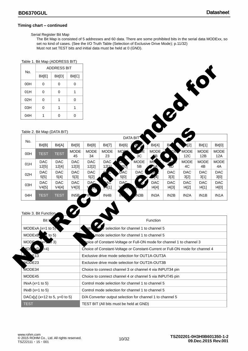
Timing chart – continued
Serial Register Bit Map
The Bit Map is consisted of 5 addresses and 60 data. There are some prohibited bits in the serial data MODExx, so
set no kind of cases. (See the I/O Truth Table (Selection of Exclusive Drive Mode); p.11/32)
Must not set TEST bits and initial data must be held at 0 (GND).
Table 1. Bit Map (ADDRESS BIT)
No. ADDRESS BIT
Bit[E] Bit[D] Bit[C]
00H 0 0 0
01H 0 0 1
02H 0 1 0
03H 0 1 1
04H 1 0 0
Table 2. Bit Map (DATA BIT)
No. DATA BIT
Bit[B] Bit[A] Bit[9] Bit[8] Bit[7] Bit[6] Bit[5] Bit[4] Bit[3] Bit[2] Bit[1] Bit[0]
00H TEST TEST MODE
45
MODE
34
MODE
23
MODE
13
MODE
3C
MODE
3B
MODE
3A
MODE
12C
MODE
12B
MODE
12A
01H DAC
12[5]
DAC
12[4]
DAC
12[3]
DAC
12[2]
DAC
12[1]
DAC
12[0]
MODE
5B
MODE
5A
MODE
4D
MODE
4C
MODE
4B
MODE
4A
02H DAC
5[5]
DAC
5[4]
DAC
5[3]
DAC
5[2]
DAC
5[1]
DAC
5[0]
DAC
3[5]
DAC
3[4]
DAC
3[3]
DAC
3[2]
DAC
3[1]
DAC
3[0]
03H DAC
V4[5]
DAC
V4[4]
DAC
V4[3]
DAC
V4[2]
DAC
V4[1]
DAC
V4[0]
DAC
I4[5]
DAC
I4[4]
DAC
I4[3]
DAC
I4[2]
DAC
I4[1]
DAC
I4[0]
04H TEST TEST IN5B IN5A IN4B IN4A IN3B IN3A IN2B IN2A IN1B IN1A
Table 3. Bit Function
Bit Name Function
MODExA (x=1 to 5) Control mode selection for channel 1 to channel 5
MODExB (x=1 to 5) Control mode selection for channel 1 to channel 5
MODExC (x=1 to 3) Choice of Constant-Voltage or Full-ON mode for channel 1 to channel 3
MODExD (x=4) Choice of Constant-Voltage or Constant-Current or Full-ON mode for channel 4
MODE13 Exclusive drive mode selection for OUT1A-OUT3A
MODE23 Exclusive drive mode selection for OUT2A-OUT3B
MODE34 Choice to connect channel 3 or channel 4 via INPUT34 pin
MODE45 Choice to connect channel 4 or channel 5 via INPUT45 pin
INxA (x=1 to 5) Control mode selection for channel 1 to channel 5
INxB (x=1 to 5) Control mode selection for channel 1 to channel 5
DACx[y] (x=12 to 5, y=0 to 5) D/A Converter output selection for channel 1 to channel 5
TEST TEST BIT (All bits must be held at GND)
Not R
ecom
men
ded
for
New D
esig
ns

11/32
TSZ02201-0H3H0B601350-1-2 © 2015 ROHM Co., Ltd. All rights reserved. www.rohm.com
TSZ22111・15・001
BD6370GUL
09.Dec.2015 Rev.001
Timing chart – continued
Table 4. DATA BIT MAP [000]
ADR. DATA BIT
Bit[B] Bit[A] Bit[9] Bit[8] Bit[7] Bit[6] Bit[5] Bit[4] Bit[3] Bit[2] Bit[1] Bit[0]
000 TEST (Note 5)
TEST (Note 5)
MODE
45
MODE
34
MODE
23
MODE
13
MODE
3C
MODE
3B
MODE
3A
MODE
12C
MODE
12B
MODE
12A (Note 5) Must be held at 0 (GND)
Refer to the p.19/32 to p.21/32 about MODE12A & MODE12B. Refer to the p.20/32 about MODE3A & MODE3B.
Table 5. I/O Truth Table for Drive Mode Selection (Channel 1 to Channel 3)
Bit[5] Bit[2] Drive Mode for Output Terminals Note
MODE3C MODE12C Channel 3 Channel 2 Channel 1
0 - Full-ON - - DAC3: 6’b111111
1 - Constant-Voltage - -
- 0 - Full-ON Full-ON DAC12: 6’b111111
- 1 - Constant-Voltage Constant-Voltage
Table 6. I/O Truth Table for Exclusive Drive Mode Selection
Bit[9] Bit[8] Bit[7] Bit[6] Input Pins Correspond to Outputs Note
MODE 45
MODE 34
MODE 23
MODE 13
INPUT 45
INPUT 34
INPUT 2
INPUT 1
Opened Output Terminals Ref No.
(Next)
0 0 0 0 OUT
4A-4B OUT
3A-3B OUT
2A-2B OUT
1A-1B OUT5A, 5B 1
0(Note 6) 0 0 1
0(Note 6) 0 1 0
0(Note 6) 0 1 1
0 1 0 0 OUT
5A-5B OUT
4A-4B OUT
2A-2B OUT
1A-1B OUT3A, 3B 2
0 1 0 1 OUT
5A-5B OUT
4A-4B OUT
2A-2B OUT
1A-3A OUT1B, 3B 3
0 1 1 0 OUT
5A-5B OUT
4A-4B OUT
2A-3B OUT
1A-1B OUT2B, 3A 4
0 1 1 1 OUT
5A-5B OUT
4A-4B OUT
2A-3B OUT
1A-3A OUT1B, 2B 5
1 0 0 0 OUT
5A-5B OUT
3A-3B OUT
2A-2B OUT
1A-1B OUT4A, 4B 6
1(Note 6) 0 0 1
1(Note 6) 0 1 0
1(Note 6) 0 1 1
1(Note 6) 1 0 0
1(Note 6) 1 0 1
1(Note 6) 1 1 0
1(Note 6) 1 1 1
(Note 6) Must not set data
Not R
ecom
men
ded
for
New D
esig
ns

12/32
TSZ02201-0H3H0B601350-1-2 © 2015 ROHM Co., Ltd. All rights reserved. www.rohm.com
TSZ22111・15・001
BD6370GUL
09.Dec.2015 Rev.001
Timing chart – continued
(Note 7) C.V.=Constant-Voltage drive mode Full ON=Full-ON drive mode C.C.=Constant-Current drive mode STM=Stepping Motor DCM=DC Motor VCM=Voice Coil Motor
(Note 7)
OUT3A
OUT3B
OUT1A
OUT1B
OUT2A
OUT2B
M
OUT4A
OUT4B
OUT5A
OUT5B
Auto
Focus (STM)
Zoom (DCM)
Iris (VCM)
Shutter
(VCM)
INPUT1
INPUT2
ch1
C.V./Full ON
ch2
C.V./Full ON
INPUT34
INPUT45
ch4
C.V./C.C./Full ON
ch3
C.V./Full ON
ch5
C.C.
Figure 5. Example of Standard Model
(Ref. No.1, 2, and 6)
(Note 7)
OUT3A
OUT3B
OUT1A
OUT1B
OUT2A
OUT2B
M
OUT4A
OUT4B
OUT5A
OUT5B
M Iris or Zoom (STM)
Shutter
(VCM)
INPUT1
INPUT2
ch1
C.V./Full ON
ch2
C.V./Full ON
INPUT34
INPUT45
ch4
C.V./C.C./Full ON
ch5
C.C.
ch3
C.V./Full ON
Auto Focus (STM)
Zoom or Iris (DCM, VCM)
Figure 6. Example of High Performance Model
(Ref. No.2 and 5)
(Note 7)
other actuator;
LED etc.
OUT3A
OUT3B
OUT1A
OUT1B
OUT2A
OUT2B
M
OUT4A
OUT4B
OUT5A
OUT5B
Zoom
(DCM)
Shutter (VCM)
INPUT1
INPUT2
ch1
C.V./Full ON
ch2
C.V./Full ON
INPUT34
INPUT45
ch4
C.V./C.C./Full ON
ch5
C.C.
ch3
C.V./Full ON
Iris (VCM)
Auto Focus (STM)
Figure 7. Example 1 of Standard Model and
another Actuator (Ref. No.3 and 6)
(Note 7)
other actuator;
LED etc.
OUT3A
OUT3B
OUT1A
OUT1B
OUT2A
OUT2B
M
OUT4A
OUT4B
OUT5A
OUT5B
Iris
(VCM)
Zoom (DCM)
Shutter
(VCM)
INPUT1
INPUT2
ch1
C.V./Full ON
ch2
C.V./Full ON
INPUT34
INPUT45
ch4
C.V./C.C./Full ON
ch5
C.C.
ch3
C.V./Full ON
Figure 8. Example 2 of Standard Model and
another Actuator (Ref. No.4 and 6)
Auto
Focus (STM)
Not R
ecom
men
ded
for
New D
esig
ns

13/32
TSZ02201-0H3H0B601350-1-2 © 2015 ROHM Co., Ltd. All rights reserved. www.rohm.com
TSZ22111・15・001
BD6370GUL
09.Dec.2015 Rev.001
Timing chart – continued
Table 7. DATA BIT MAP [001]
ADR. DATA BIT
Bit[B] Bit[A] Bit[9] Bit[8] Bit[7] Bit[6] Bit[5] Bit[4] Bit[3] Bit[2] Bit[1] Bit[0]
001 DAC 12[5]
DAC 12[4]
DAC 12[3]
DAC 12[2]
DAC 12[1]
DAC 12[0]
MODE 5B
MODE 5A
MODE 4D
MODE 4C
MODE 4B
MODE 4A
Refer to the p.22/32 about MODE4A & MODE4B. Refer to the p.23/32 about MODE5A & MODE5B.
Table 8. Function Table for Output Drive Mode Selection (Channel 4)
Bit[3] Bit[2] Drive Mode Note
MODE4D MODE4C
0 0 Full-ON DACV4=DACI4: 6’b111111,
RNF4 pin should be directly connected to ground
0 1 Full-ON DACV4=DACI4: 6’b111111,
RNF4 pin should be directly connected to ground
1 0 Constant Voltage DACI4: 6’b111111,
RNF4 pin should be directly connected to ground
1 1 Constant Current DACV4: 6’b111111,
RNF4 pin with resistor should be connected to ground
Not R
ecom
men
ded
for
New D
esig
ns

14/32
TSZ02201-0H3H0B601350-1-2 © 2015 ROHM Co., Ltd. All rights reserved. www.rohm.com
TSZ22111・15・001
BD6370GUL
09.Dec.2015 Rev.001
Timing chart – continued
Table 9. Function Table for Output Voltage in case of Constant Voltage Mode (Channel 1 & Channel 2)
Bit[B] Bit[A] Bit[9] Bit[8] Bit[7] Bit[6] DAC12 Voltage;
VDAC12 [V]
Output High
Voltage; VOH [V] DAC12[5] DAC12[4] DAC12[3] DAC12[2] DAC12[1] DAC12[0]
0 1 0 1 0 0 0.188 1.500
0 1 0 1 0 1 0.197 1.575
0 1 0 1 1 0 0.206 1.650
0 1 0 1 1 1 0.216 1.725
0 1 1 0 0 0 0.225 1.800
0 1 1 0 0 1 0.234 1.875
0 1 1 0 1 0 0.244 1.950
0 1 1 0 1 1 0.253 2.025
0 1 1 1 0 0 0.263 2.100
0 1 1 1 0 1 0.272 2.175
0 1 1 1 1 0 0.281 2.250
0 1 1 1 1 1 0.291 2.325
1 0 0 0 0 0 0.300 2.400
1 0 0 0 0 1 0.309 2.475
1 0 0 0 1 0 0.319 2.550
1 0 0 0 1 1 0.328 2.625
1 0 0 1 0 0 0.338 2.700
1 0 0 1 0 1 0.347 2.775
1 0 0 1 1 0 0.356 2.850
1 0 0 1 1 1 0.366 2.925
1 0 1 0 0 0 0.375 3.000
1 0 1 0 0 1 0.384 3.075
1 0 1 0 1 0 0.394 3.150
1 0 1 0 1 1 0.403 3.225
1 0 1 1 0 0 0.413 3.300
1 0 1 1 0 1 0.422 3.375
1 0 1 1 1 0 0.431 3.450
1 0 1 1 1 1 0.441 3.525
1 1 0 0 0 0 0.450 3.600
1 1 0 0 0 1 0.459 3.675
1 1 0 0 1 0 0.469 3.750
1 1 0 0 1 1 0.478 3.825
1 1 0 1 0 0 0.488 3.900
1 1 0 1 0 1 0.497 3.975
1 1 0 1 1 0 0.506 4.050
1 1 0 1 1 1 0.516 4.125
1 1 1 0 0 0 0.525 4.200
1 1 1 0 0 1 0.534 4.275
1 1 1 0 1 0 0.544 4.350
1 1 1 0 1 1 0.553 4.425
1 1 1 1 0 0 0.563 4.500
1 1 1 1 0 1 0.572 4.575
1 1 1 1 1 0 0.581 4.650
1 1 1 1 1 1 0.591 4.725
Not R
ecom
men
ded
for
New D
esig
ns

15/32
TSZ02201-0H3H0B601350-1-2 © 2015 ROHM Co., Ltd. All rights reserved. www.rohm.com
TSZ22111・15・001
BD6370GUL
09.Dec.2015 Rev.001
Timing chart – continued
Table 10. DATA BIT MAP [010]
ADR. DATA BIT
Bit[B] Bit[A] Bit[9] Bit[8] Bit[7] Bit[6] Bit[5] Bit[4] Bit[3] Bit[2] Bit[1] Bit[0]
010 DAC 5[5]
DAC 5[4]
DAC 5[3]
DAC 5[2]
DAC 5[1]
DAC 5[0]
DAC 3[5]
DAC 3[4]
DAC 3[3]
DAC 3[2]
DAC 3[1]
DAC 3[0]
Table 11. Function Table for Output Voltage in case of Constant Voltage Mode (Channel 3)
Bit[5] Bit[4] Bit[3] Bit[2] Bit[1] Bit[0] DAC3 Voltage;
VDAC3 [V]
Output High
Voltage; VOH [V] DAC3[5] DAC3[4] DAC3[3] DAC3[2] DAC3[1] DAC3[0]
0 1 0 1 0 0 0.188 1.500
0 1 0 1 0 1 0.197 1.575
0 1 0 1 1 0 0.206 1.650
0 1 0 1 1 1 0.216 1.725
0 1 1 0 0 0 0.225 1.800
0 1 1 0 0 1 0.234 1.875
0 1 1 0 1 0 0.244 1.950
0 1 1 0 1 1 0.253 2.025
0 1 1 1 0 0 0.263 2.100
0 1 1 1 0 1 0.272 2.175
0 1 1 1 1 0 0.281 2.250
0 1 1 1 1 1 0.291 2.325
1 0 0 0 0 0 0.300 2.400
1 0 0 0 0 1 0.309 2.475
1 0 0 0 1 0 0.319 2.550
1 0 0 0 1 1 0.328 2.625
1 0 0 1 0 0 0.338 2.700
1 0 0 1 0 1 0.347 2.775
1 0 0 1 1 0 0.356 2.850
1 0 0 1 1 1 0.366 2.925
1 0 1 0 0 0 0.375 3.000
1 0 1 0 0 1 0.384 3.075
1 0 1 0 1 0 0.394 3.150
1 0 1 0 1 1 0.403 3.225
1 0 1 1 0 0 0.413 3.300
1 0 1 1 0 1 0.422 3.375
1 0 1 1 1 0 0.431 3.450
1 0 1 1 1 1 0.441 3.525
1 1 0 0 0 0 0.450 3.600
1 1 0 0 0 1 0.459 3.675
1 1 0 0 1 0 0.469 3.750
1 1 0 0 1 1 0.478 3.825
1 1 0 1 0 0 0.488 3.900
1 1 0 1 0 1 0.497 3.975
1 1 0 1 1 0 0.506 4.050
1 1 0 1 1 1 0.516 4.125
1 1 1 0 0 0 0.525 4.200
1 1 1 0 0 1 0.534 4.275
1 1 1 0 1 0 0.544 4.350
1 1 1 0 1 1 0.553 4.425
1 1 1 1 0 0 0.563 4.500
1 1 1 1 0 1 0.572 4.575
1 1 1 1 1 0 0.581 4.650
1 1 1 1 1 1 0.591 4.725
Not R
ecom
men
ded
for
New D
esig
ns

16/32
TSZ02201-0H3H0B601350-1-2 © 2015 ROHM Co., Ltd. All rights reserved. www.rohm.com
TSZ22111・15・001
BD6370GUL
09.Dec.2015 Rev.001
Timing chart – continued
Table 12. Function Table for Output Current in case of Constant Current Mode (Channel 5)
Bit[B] Bit[A] Bit[9] Bit[8] Bit[7] Bit[6] DAC5 Voltage
VDAC5 [mV]
RRNF5=0.5Ω
Current [mA]
RRNF5=1.0Ω
Current [mA] DAC5[5] DAC5[4] DAC5[3] DAC5[2] DAC5[1] DAC5[0]
0 0 1 0 1 0 50 96 49
0 0 1 0 1 1 55 105 54
0 0 1 1 0 0 60 115 59
0 0 1 1 0 1 65 125 64
0 0 1 1 1 0 70 134 68
0 0 1 1 1 1 75 144 73
0 1 0 0 0 0 80 153 78
0 1 0 0 0 1 85 163 83
0 1 0 0 1 0 90 172 88
0 1 0 0 1 1 95 182 93
0 1 0 1 0 0 100 192 98
0 1 0 1 0 1 105 201 103
0 1 0 1 1 0 110 211 108
0 1 0 1 1 1 115 220 113
0 1 1 0 0 0 120 230 117
0 1 1 0 0 1 125 239 122
0 1 1 0 1 0 130 249 127
0 1 1 0 1 1 135 259 132
0 1 1 1 0 0 140 268 137
0 1 1 1 0 1 145 278 142
0 1 1 1 1 0 150 287 147
0 1 1 1 1 1 155 297 152
1 0 0 0 0 0 160 307 157
1 0 0 0 0 1 165 316 161
1 0 0 0 1 0 170 326 166
1 0 0 0 1 1 175 336 171
1 0 0 1 0 0 180 345 176
1 0 0 1 0 1 185 355 181
1 0 0 1 1 0 190 364 186
1 0 0 1 1 1 195 374 191
1 0 1 0 0 0 200 383 196
1 0 1 0 0 1 205 393 201
1 0 1 0 1 0 210
Over
Operating
Condition
205
1 0 1 0 1 1 215 210
1 0 1 1 0 0 220 216
1 0 1 1 0 1 225 220
1 0 1 1 1 0 230 225
1 0 1 1 1 1 235 230
1 1 0 0 0 0 240 235
1 1 0 0 0 1 245 240
1 1 0 0 1 0 250 245
1 1 0 0 1 1 255 250
1 1 0 1 0 0 260 254
1 1 0 1 0 1 265 259
1 1 0 1 1 0 270 264
1 1 0 1 1 1 275 269
1 1 1 0 0 0 280 274
1 1 1 0 0 1 285 279
1 1 1 0 1 0 290 284
1 1 1 0 1 1 295 289
1 1 1 1 0 0 300 294
1 1 1 1 0 1 305 298
1 1 1 1 1 0 310 303
1 1 1 1 1 1 315 308
Not R
ecom
men
ded
for
New D
esig
ns

17/32
TSZ02201-0H3H0B601350-1-2 © 2015 ROHM Co., Ltd. All rights reserved. www.rohm.com
TSZ22111・15・001
BD6370GUL
09.Dec.2015 Rev.001
Timing chart – continued
Table 13. DATA BIT MAP [011]
ADR. DATA BIT
Bit[B] Bit[A] Bit[9] Bit[8] Bit[7] Bit[6] Bit[5] Bit[4] Bit[3] Bit[2] Bit[1] Bit[0]
011 DAC V4[5]
DAC V4[4]
DAC V4[3]
DAC V4[2]
DAC V4[1]
DAC V4[0]
DAC I4[5]
DAC I4[4]
DAC I4[3]
DAC I4[2]
DAC I4[1]
DAC I4[0]
Table 14. Function Table for Output Voltage in case of Constant Voltage Mode (Channel 4)
Bit[B] Bit[A] Bit[9] Bit[8] Bit[7] Bit[6] DACV4 Voltage VDACV4 [V]
Output High Voltage; VOH [V] DACV4[5] DACV4[4] DACV4[3] DACV4[2] DACV4[1] DACV4[0]
0 1 0 1 0 0 0.188 1.500
0 1 0 1 0 1 0.197 1.575
0 1 0 1 1 0 0.206 1.650
0 1 0 1 1 1 0.216 1.725
0 1 1 0 0 0 0.225 1.800
0 1 1 0 0 1 0.234 1.875
0 1 1 0 1 0 0.244 1.950
0 1 1 0 1 1 0.253 2.025
0 1 1 1 0 0 0.263 2.100
0 1 1 1 0 1 0.272 2.175
0 1 1 1 1 0 0.281 2.250
0 1 1 1 1 1 0.291 2.325
1 0 0 0 0 0 0.300 2.400
1 0 0 0 0 1 0.309 2.475
1 0 0 0 1 0 0.319 2.550
1 0 0 0 1 1 0.328 2.625
1 0 0 1 0 0 0.338 2.700
1 0 0 1 0 1 0.347 2.775
1 0 0 1 1 0 0.356 2.850
1 0 0 1 1 1 0.366 2.925
1 0 1 0 0 0 0.375 3.000
1 0 1 0 0 1 0.384 3.075
1 0 1 0 1 0 0.394 3.150
1 0 1 0 1 1 0.403 3.225
1 0 1 1 0 0 0.413 3.300
1 0 1 1 0 1 0.422 3.375
1 0 1 1 1 0 0.431 3.450
1 0 1 1 1 1 0.441 3.525
1 1 0 0 0 0 0.450 3.600
1 1 0 0 0 1 0.459 3.675
1 1 0 0 1 0 0.469 3.750
1 1 0 0 1 1 0.478 3.825
1 1 0 1 0 0 0.488 3.900
1 1 0 1 0 1 0.497 3.975
1 1 0 1 1 0 0.506 4.050
1 1 0 1 1 1 0.516 4.125
1 1 1 0 0 0 0.525 4.200
1 1 1 0 0 1 0.534 4.275
1 1 1 0 1 0 0.544 4.350
1 1 1 0 1 1 0.553 4.425
1 1 1 1 0 0 0.563 4.500
1 1 1 1 0 1 0.572 4.575
1 1 1 1 1 0 0.581 4.650
1 1 1 1 1 1 0.591 4.725
Not R
ecom
men
ded
for
New D
esig
ns

18/32
TSZ02201-0H3H0B601350-1-2 © 2015 ROHM Co., Ltd. All rights reserved. www.rohm.com
TSZ22111・15・001
BD6370GUL
09.Dec.2015 Rev.001
Timing chart – continued
Table 15. Function Table for Output Current in case of Constant Current Mode (Channel 4)
Bit[5] Bit[4] Bit[3] Bit[2] Bit[1] Bit[0] DACI4 Voltage
VDACI4 [mV]
RRNFI4=0.5Ω
Current [mA]
RRNFI4=1.0Ω
Current [mA] DACI4[5] DACI4[4] DACI4[3] DACI4[2] DACI4[1] DACI4[0]
0 0 1 0 1 0 50 99 50
0 0 1 0 1 1 55 109 55
0 0 1 1 0 0 60 119 60
0 0 1 1 0 1 65 129 65
0 0 1 1 1 0 70 139 70
0 0 1 1 1 1 75 149 75
0 1 0 0 0 0 80 159 80
0 1 0 0 0 1 85 169 85
0 1 0 0 1 0 90 179 90
0 1 0 0 1 1 95 188 95
0 1 0 1 0 0 100 198 100
0 1 0 1 0 1 105 208 105
0 1 0 1 1 0 110 218 110
0 1 0 1 1 1 115 228 115
0 1 1 0 0 0 120 238 120
0 1 1 0 0 1 125 248 125
0 1 1 0 1 0 130 258 129
0 1 1 0 1 1 135 268 134
0 1 1 1 0 0 140 278 139
0 1 1 1 0 1 145 288 144
0 1 1 1 1 0 150 298 149
0 1 1 1 1 1 155 308 154
1 0 0 0 0 0 160 317 159
1 0 0 0 0 1 165 327 164
1 0 0 0 1 0 170 337 169
1 0 0 0 1 1 175 347 174
1 0 0 1 0 0 180 357 179
1 0 0 1 0 1 185 367 184
1 0 0 1 1 0 190 377 189
1 0 0 1 1 1 195 387 194
1 0 1 0 0 0 200 397 199
1 0 1 0 0 1 205
Over
Operating
Condition
204
1 0 1 0 1 0 210 209
1 0 1 0 1 1 215 214
1 0 1 1 0 0 220 219
1 0 1 1 0 1 225 224
1 0 1 1 1 0 230 229
1 0 1 1 1 1 235 234
1 1 0 0 0 0 240 239
1 1 0 0 0 1 245 244
1 1 0 0 1 0 250 249
1 1 0 0 1 1 255 254
1 1 0 1 0 0 260 259
1 1 0 1 0 1 265 264
1 1 0 1 1 0 270 269
1 1 0 1 1 1 275 274
1 1 1 0 0 0 280 279
1 1 1 0 0 1 285 284
1 1 1 0 1 0 290 289
1 1 1 0 1 1 295 294
1 1 1 1 0 0 300 299
1 1 1 1 0 1 305 304
1 1 1 1 1 0 310 309
1 1 1 1 1 1 315 314
Not R
ecom
men
ded
for
New D
esig
ns

19/32
TSZ02201-0H3H0B601350-1-2 © 2015 ROHM Co., Ltd. All rights reserved. www.rohm.com
TSZ22111・15・001
BD6370GUL
09.Dec.2015 Rev.001
Timing chart – continued
Table 16. DATA BIT MAP [100]
ADR. DATA BIT
Bit[B] Bit[A] Bit[9] Bit[8] Bit[7] Bit[6] Bit[5] Bit[4] Bit[3] Bit[2] Bit[1] Bit[0]
100 TEST (Note 8)
TEST (Note 8)
IN5B IN5A IN4B IN4A IN3B IN3A IN2B IN2A IN1B IN1A
(Note 8) Must be held at 0 (GND)
Table 17. I/O Truth Table (Channel 1)
Serial Interface Bit INPUT OUTPUT
MODE 23
MODE 13
MODE
12B
MODE
12A IN1B IN1A INPUT1 OUT1A OUT1B Output Mode (Note 9)
PWM Drive Mode via INPUT1 Pin
0 0 0 0 0 0 X Z Z Open
0 0 0 0 0 1 L L L Short Brake
0 0 0 0 0 1 H H L CW
0 0 0 0 1 0 L L L Short Brake
0 0 0 0 1 0 H L H CCW
0 0 0 0 1 1 X L L Short Brake
PWM Drive Mode via INPUT1 Pin
0 0 0 1 0 0 X Z Z Open
0 0 0 1 0 1 L H L CW
0 0 0 1 0 1 H L L Short Brake
0 0 0 1 1 0 L L H CCW
0 0 0 1 1 0 H L L Short Brake
0 0 0 1 1 1 X L L Short Brake
CW / CCW Drive Mode via INPUT1 Pin
0 0 1 0 X 0 X Z Z Open
0 0 1 0 0 1 L L H CCW
0 0 1 0 0 1 H H L CW
0 0 1 0 1 1 X L L Short Brake
CW / CCW Drive Mode via INPUT1 Pin
0 0 1 1 X 0 X Z Z Open
0 0 1 1 0 1 L H L CW
0 0 1 1 0 1 H L H CCW
0 0 1 1 1 1 X L L Short Brake L: Low, H: High, X: Don’t care, Z: Hi impedance
(Note 9) CW: Current flows from OUT1A to OUT1B, CCW: Current flows from OUT1B to OUT1A
Not R
ecom
men
ded
for
New D
esig
ns

20/32
TSZ02201-0H3H0B601350-1-2 © 2015 ROHM Co., Ltd. All rights reserved. www.rohm.com
TSZ22111・15・001
BD6370GUL
09.Dec.2015 Rev.001
Timing chart – continued
Table 18. I/O Truth Table (Channel 2)
Serial Interface Bit INPUT OUTPUT
MODE 23
MODE 13
MODE
12B
MODE
12A IN2B IN2A INPUT2 OUT2A OUT2B Output Mode (Note 10)
PWM Drive Mode via INPUT2 Pin
0 0 0 0 0 0 X Z Z Open
0 0 0 0 0 1 L L L Short Brake
0 0 0 0 0 1 H H L CW
0 0 0 0 1 0 L L L Short Brake
0 0 0 0 1 0 H L H CCW
0 0 0 0 1 1 X L L Short Brake
PWM Drive Mode via INPUT2 Pin
0 0 0 1 0 0 X Z Z Open
0 0 0 1 0 1 L H L CW
0 0 0 1 0 1 H L L Short Brake
0 0 0 1 1 0 L L H CCW
0 0 0 1 1 0 H L L Short Brake
0 0 0 1 1 1 X L L Short Brake
CW / CCW Drive Mode via INPUT2 Pin
0 0 1 0 X 0 X Z Z Open
0 0 1 0 0 1 L L H CCW
0 0 1 0 0 1 H H L CW
0 0 1 0 1 1 X L L Short Brake
CW / CCW Drive Mode via INPUT2 Pin
0 0 1 1 X 0 X Z Z Open
0 0 1 1 0 1 L H L CW
0 0 1 1 0 1 H L H CCW
0 0 1 1 1 1 X L L Short Brake L: Low, H: High, X: Don’t care, Z: Hi impedance
(Note 10) CW: Current flows from OUT2A to OUT2B, CCW: Current flows from OUT2B to OUT2A
Table 19. I/O Truth Table (Channel 3)
Serial Interface Bit INPUT OUTPUT
MODE 34
MODE 23
MODE
3B
MODE
3A IN3B IN3A INPUT34 OUT3A OUT3B Output Mode (Note 11)
PWM Drive Mode via INPUT34 Pin
0 0 0 0 0 0 X Z Z Open
0 0 0 0 0 1 L L L Short Brake
0 0 0 0 0 1 H H L CW
0 0 0 0 1 0 L L L Short Brake
0 0 0 0 1 0 H L H CCW
0 0 0 0 1 1 X L L Short Brake
PWM Drive Mode via INPUT34 Pin
0 0 0 1 0 0 X Z Z Open
0 0 0 1 0 1 L H L CW
0 0 0 1 0 1 H L L Short Brake
0 0 0 1 1 0 L L H CCW
0 0 0 1 1 0 H L L Short Brake
0 0 0 1 1 1 X L L Short Brake
CW / CCW Drive Mode via INPUT34 Pin
0 0 1 0 X 0 X Z Z Open
0 0 1 0 0 1 L L H CCW
0 0 1 0 0 1 H H L CW
0 0 1 0 1 1 X L L Short Brake
CW / CCW Drive Mode via INPUT34 Pin
0 0 1 1 X 0 X Z Z Open
0 0 1 1 0 1 L H L CW
0 0 1 1 0 1 H L H CCW
0 0 1 1 1 1 X L L Short Brake L: Low, H: High, X: Don’t care, Z: Hi impedance
(Note 11) CW: Current flows from OUT3A to OUT3B, CCW: Current flows from OUT3B to OUT3A
Not R
ecom
men
ded
for
New D
esig
ns

21/32
TSZ02201-0H3H0B601350-1-2 © 2015 ROHM Co., Ltd. All rights reserved. www.rohm.com
TSZ22111・15・001
BD6370GUL
09.Dec.2015 Rev.001
Timing chart – continued
Table 20. I/O Truth Table (Exclusive Drive Mode for OUT1A-OUT3A)
Serial Interface Bit INPUT OUTPUT
MODE 23
MODE 13
MODE
12B
MODE
12A IN1B IN1A INPUT1 OUT1A OUT3A Output Mode (Note 12)
PWM Drive Mode via INPUT1 Pin
ANY 1 0 0 0 0 X Z Z Open
ANY 1 0 0 0 1 L L L Short Brake
ANY 1 0 0 0 1 H H L CW
ANY 1 0 0 1 0 L L L Short Brake
ANY 1 0 0 1 0 H L H CCW
ANY 1 0 0 1 1 X L L Short Brake
PWM Drive Mode via INPUT1 Pin
ANY 1 0 1 0 0 X Z Z Open
ANY 1 0 1 0 1 L H L CW
ANY 1 0 1 0 1 H L L Short Brake
ANY 1 0 1 1 0 L L H CCW
ANY 1 0 1 1 0 H L L Short Brake
ANY 1 0 1 1 1 X L L Short Brake
CW / CCW Drive Mode via INPUT1 Pin
ANY 1 1 0 X 0 X Z Z Open
ANY 1 1 0 0 1 L L H CCW
ANY 1 1 0 0 1 H H L CW
ANY 1 1 0 1 1 X L L Short Brake
CW / CCW Drive Mode via INPUT1 Pin
ANY 1 1 1 X 0 X Z Z Open
ANY 1 1 1 0 1 L H L CW
ANY 1 1 1 0 1 H L H CCW
ANY 1 1 1 1 1 X L L Short Brake L: Low, H: High, X: Don’t care, Z: Hi impedance
(Note 12) CW: Current flows from OUT1A to OUT3A, CCW: Current flows from OUT3A to OUT1A
Table 21. I/O Truth Table (Exclusive Drive Mode for OUT2A-OUT3B)
Serial Interface Bit INPUT OUTPUT
MODE 23
MODE 13
MODE12B
MODE12A
IN2B IN2A INPUT2 OUT2A OUT3B Output Mode (Note 13)
PWM Drive Mode via INPUT2 Pin
1 ANY 0 0 0 0 X Z Z Open
1 ANY 0 0 0 1 L L L Short Brake
1 ANY 0 0 0 1 H H L CW
1 ANY 0 0 1 0 L L L Short Brake
1 ANY 0 0 1 0 H L H CCW
1 ANY 0 0 1 1 X L L Short Brake
PWM Drive Mode via INPUT2 Pin
1 ANY 0 1 0 0 X Z Z Open
1 ANY 0 1 0 1 L H L CW
1 ANY 0 1 0 1 H L L Short Brake
1 ANY 0 1 1 0 L L H CCW
1 ANY 0 1 1 0 H L L Short Brake
1 ANY 0 1 1 1 X L L Short Brake
CW / CCW Drive Mode via INPUT2 Pin
1 ANY 1 0 X 0 X Z Z Open
1 ANY 1 0 0 1 L L H CCW
1 ANY 1 0 0 1 H H L CW
1 ANY 1 0 1 1 X L L Short Brake
CW / CCW Drive Mode via INPUT2 Pin
1 ANY 1 1 X 0 X Z Z Open
1 ANY 1 1 0 1 L H L CW
1 ANY 1 1 0 1 H L H CCW
1 ANY 1 1 1 1 X L L Short Brake L: Low, H: High, X: Don’t care, Z: Hi impedance
(Note 13) CW: Current flows from OUT2A to OUT3B, CCW: Current flows from OUT3B to OUT2A
Not R
ecom
men
ded
for
New D
esig
ns

22/32
TSZ02201-0H3H0B601350-1-2 © 2015 ROHM Co., Ltd. All rights reserved. www.rohm.com
TSZ22111・15・001
BD6370GUL
09.Dec.2015 Rev.001
Timing chart – continued
Table 22. I/O Truth Table (Channel 4, Driving via INPUT34 pin)
Serial Interface Bit INPUT OUTPUT
MODE 45
MODE 34
MODE 4B
MODE 4A
IN4B IN4A INPUT34 OUT4A OUT4B Output Mode (Note 14)
PWM Drive Mode via INPUT34 Pin
0 1 0 0 0 0 X Z Z Open
0 1 0 0 0 1 L L L Short Brake
0 1 0 0 0 1 H H L CW
0 1 0 0 1 0 L L L Short Brake
0 1 0 0 1 0 H L H CCW
0 1 0 0 1 1 X L L Short Brake
PWM Drive Mode via INPUT34 Pin
0 1 0 1 0 0 X Z Z Open
0 1 0 1 0 1 L H L CW
0 1 0 1 0 1 H L L Short Brake
0 1 0 1 1 0 L L H CCW
0 1 0 1 1 0 H L L Short Brake
0 1 0 1 1 1 X L L Short Brake
CW / CCW Drive Mode via INPUT34 Pin
0 1 1 0 X 0 X Z Z Open
0 1 1 0 0 1 L L H CCW
0 1 1 0 0 1 H H L CW
0 1 1 0 1 1 X L L Short Brake
CW / CCW Drive Mode via INPUT34 Pin
0 1 1 1 X 0 X Z Z Open
0 1 1 1 0 1 L H L CW
0 1 1 1 0 1 H L H CCW
0 1 1 1 1 1 X L L Short Brake L: Low, H: High, X: Don’t care, Z: Hi impedance
(Note 14) CW: Current flows from OUT4A to OUT4B, CCW: Current flows from OUT4B to OUT4A
Table 23. I/O Truth Table (Channel 4, Driving via INPUT45 pin)
Serial Interface Bit INPUT OUTPUT
MODE 45
MODE 34
MODE 4B
MODE 4A
IN4B IN4A INPUT45 OUT4A OUT4B Output Mode (Note 15)
PWM Drive Mode via INPUT45 Pin
0 0 0 0 0 0 X Z Z Open
0 0 0 0 0 1 L L L Short Brake
0 0 0 0 0 1 H H L CW
0 0 0 0 1 0 L L L Short Brake
0 0 0 0 1 0 H L H CCW
0 0 0 0 1 1 X L L Short Brake
PWM Drive Mode via INPUT45 Pin
0 0 0 1 0 0 X Z Z Open
0 0 0 1 0 1 L H L CW
0 0 0 1 0 1 H L L Short Brake
0 0 0 1 1 0 L L H CCW
0 0 0 1 1 0 H L L Short Brake
0 0 0 1 1 1 X L L Short Brake
CW / CCW Drive Mode via INPUT45 Pin
0 0 1 0 X 0 X Z Z Open
0 0 1 0 0 1 L L H CCW
0 0 1 0 0 1 H H L CW
0 0 1 0 1 1 X L L Short Brake
CW / CCW Drive Mode via INPUT45 Pin
0 0 1 1 X 0 X Z Z Open
0 0 1 1 0 1 L H L CW
0 0 1 1 0 1 H L H CCW
0 0 1 1 1 1 X L L Short Brake L: Low, H: High, X: Don’t care, Z: Hi impedance
(Note 15) CW: Current flows from OUT4A to OUT4B, CCW: Current flows from OUT4B to OUT4A
Not R
ecom
men
ded
for
New D
esig
ns

23/32
TSZ02201-0H3H0B601350-1-2 © 2015 ROHM Co., Ltd. All rights reserved. www.rohm.com
TSZ22111・15・001
BD6370GUL
09.Dec.2015 Rev.001
Timing chart – continued
Table 24. I/O Truth Table (Channel 5)
Serial Interface Bit INPUT OUTPUT
MODE 45
MODE 34
MODE 5B
MODE 5A
IN5B IN5A INPUT45 OUT5A OUT5B Output Mode (Note 16)
PWM Drive Mode via INPUT45 Pin
0 1 0 0 0 0 X Z Z Open
0 1 0 0 0 1 L L L Short Brake
0 1 0 0 0 1 H H L CW
0 1 0 0 1 0 L L L Short Brake
0 1 0 0 1 0 H L H CCW
0 1 0 0 1 1 X L L Short Brake
PWM Drive Mode via INPUT45 Pin
0 1 0 1 0 0 X Z Z Open
0 1 0 1 0 1 L H L CW
0 1 0 1 0 1 H L L Short Brake
0 1 0 1 1 0 L L H CCW
0 1 0 1 1 0 H L L Short Brake
0 1 0 1 1 1 X L L Short Brake
CW / CCW Drive Mode via INPUT45 Pin
0 1 1 0 X 0 X Z Z Open
0 1 1 0 0 1 L L H CCW
0 1 1 0 0 1 H H L CW
0 1 1 0 1 1 X L L Short Brake
CW / CCW Drive Mode via INPUT45 Pin
0 1 1 1 X 0 X Z Z Open
0 1 1 1 0 1 L H L CW
0 1 1 1 0 1 H L H CCW
0 1 1 1 1 1 X L L Short Brake L: Low, H: High, X: Don’t care, Z: Hi impedance
(Note 16) CW: Current flows from OUT5A to OUT5B, CCW: Current flows from OUT5B to OUT5A
Table 25. I/O Truth Table (Channel 5)
Serial Interface Bit INPUT OUTPUT
MODE 45
MODE 34
MODE 5B
MODE 5A
IN5B IN5A INPUT45 OUT5A OUT5B Output Mode (Note 17)
PWM Drive Mode via INPUT45 Pin
1 0 0 0 0 0 X Z Z Open
1 0 0 0 0 1 L L L Short Brake
1 0 0 0 0 1 H H L CW
1 0 0 0 1 0 L L L Short Brake
1 0 0 0 1 0 H L H CCW
1 0 0 0 1 1 X L L Short Brake
PWM Drive Mode via INPUT45 Pin
1 0 0 1 0 0 X Z Z Open
1 0 0 1 0 1 L H L CW
1 0 0 1 0 1 H L L Short Brake
1 0 0 1 1 0 L L H CCW
1 0 0 1 1 0 H L L Short Brake
1 0 0 1 1 1 X L L Short Brake
CW / CCW Drive Mode via INPUT45 Pin
1 0 1 0 X 0 X Z Z Open
1 0 1 0 0 1 L L H CCW
1 0 1 0 0 1 H H L CW
1 0 1 0 1 1 X L L Short Brake
CW / CCW Drive Mode via INPUT45 Pin
1 0 1 1 X 0 X Z Z Open
1 0 1 1 0 1 L H L CW
1 0 1 1 0 1 H L H CCW
1 0 1 1 1 1 X L L Short Brake L: Low, H: High, X: Don’t care, Z: Hi impedance
(Note 17) CW: Current flows from OUT5A to OUT5B, CCW: Current flows from OUT5B to OUT5A
Not R
ecom
men
ded
for
New D
esig
ns

24/32
TSZ02201-0H3H0B601350-1-2 © 2015 ROHM Co., Ltd. All rights reserved. www.rohm.com
TSZ22111・15・001
BD6370GUL
09.Dec.2015 Rev.001
Timing chart – continued
Table 26. I/O Truth Table for Steeping Motor in Case of 2 Phase Mode
Serial Interface Bit INPUT OUTPUT
MODE
12B
MODE
12A IN2B IN2A IN1B IN1A
INPUT
1
INPUT
2
OUT
1A
OUT
1B
OUT
2A
OUT
2B
Output Mode (Note 18)
1 0 0 1 0 1 H H H L H L 1. CW / CW
1 0 0 1 0 1 H L H L L H 2. CCW / CW
1 0 0 1 0 1 L L L H L H 3. CCW / CCW
1 0 0 1 0 1 L H L H H L 4. CW / CCW L: Low, H: High, X: Don’t care, Z: Hi impedance
(Note 18) CW: Current flows from OUTxA to OUTxB, CCW: Current flows from OUTxB to OUTxA (x=1, 2)
3 2
VCC
100%
0%
PS
100%
0%
STROBE
100%
0%
SDATA
100%
0%
INPUT2
100%
0%
INPUT1
100%
0%
OUT1A [V]
OUT1B [V]
0%
100%
0%
100%
0%
OUT2A [V]
OUT2B [V]
100%
0%
100%
0%
OUT1A-1B [A]
100%
0%
-100%
OUT2A-2B [A]
100%
0%
-100%
SCLK
100%
0%
3 2 1 3 4 2 1 3 2 1
(i) (ii) (iii) (iv) (v) (vi) (vii)
1 1
Forward Reverse ; Hi impedance ; Don’t care
4 4 4
Figure 9. Timing Chart of Stepping Motor Drive Not
Rec
omm
ende
d fo
r
New D
esig
ns

25/32
TSZ02201-0H3H0B601350-1-2 © 2015 ROHM Co., Ltd. All rights reserved. www.rohm.com
TSZ22111・15・001
BD6370GUL
09.Dec.2015 Rev.001
Timing chart – continued
Table 27. An Example of Serial Control from Initial Set Up (i) to End Timing (vii) (SDATA image in Figure 9.)
ADR. DATA BIT
Bit[B] Bit[A] Bit[9] Bit[8] Bit[7] Bit[6] Bit[5] Bit[4] Bit[3] Bit[2] Bit[1] Bit[0]
Initial set up
(i) ADDRESS BIT [000]; Setup of channel 1 & channel 2 to drive Constant-Voltage mode
000
MODE
45
MODE
34
MODE
23
MODE
13
MODE
3C
MODE
3B
MODE
3A
MODE
12C
MODE
12B
MODE
12A
0 0 0 0 0 0 0 1 1 0
(ii) ADDRESS BIT [001]; Setup of output high voltage=3.0V for channel 1 & channel 2
001
DAC
12[5]
DAC
12[4]
DAC
12[3]
DAC
12[2]
DAC
12[1]
DAC
12[0]
MODE
5B
MODE
5A
MODE
4D
MODE
4C
MODE
4B
MODE
4A
1 0 1 0 0 0 0 0 0 0 0 0
(iii) ADDRESS BIT [010]; No need in this case
010
DAC
5[5]
DAC
5[4]
DAC
5[3]
DAC
5[2]
DAC
5[1]
DAC
5[0]
DAC
3[5]
DAC
3[4]
DAC
3[3]
DAC
3[2]
DAC
3[1]
DAC
3[0]
0 0 0 0 0 0 0 0 0 0 0 0
(iv) ADDRESS BIT [011]; No need in this case
011
DAC
V4[5]
DAC
V4[4]
DAC
V4[3]
DAC
V4[2]
DAC
V4[1]
DAC
V4[0]
DAC
I4[5]
DAC
I4[4]
DAC
I4[3]
DAC
I4[2]
DAC
I4[1]
DAC
I4[0]
0 0 0 0 0 0 0 0 0 0 0 0
(v) ADDRESS BIT [100]; Setup of stand-by mode
100
IN5B IN5A IN4B IN4A IN3B IN3A IN2B IN2A IN1B IN1A
0 0 0 0 0 0 0 0 0 0
Start timing
(vi) ADDRESS BIT [100]
100
IN5B IN5A IN4B IN4A IN3B IN3A IN2B IN2A IN1B IN1A
0 0 0 0 0 0 0 1 0 1
End timing
(vii) ADDRESS BIT [100]
100
IN5B IN5A IN4B IN4A IN3B IN3A IN2B IN2A IN1B IN1A
0 0 0 0 0 0 0 0 0 0
Not
Rec
omm
ende
d fo
r
New D
esig
ns

26/32
TSZ02201-0H3H0B601350-1-2 © 2015 ROHM Co., Ltd. All rights reserved. www.rohm.com
TSZ22111・15・001
BD6370GUL
09.Dec.2015 Rev.001
Application Example
Selection of Components Externally Connected
When using the circuit with changes to the external circuit constants, make sure to leave an adequate margin for external components including static and transitional characteristics as well as dispersion of the IC.
Level Shift
&
Pre Driver
6bit DAC3 VDAC3
OUT3A
OUT3B
H bridge
C.V./Full ON
PGND
PS
VCC
1µF to 100µF
OUT1A
OUT1B Level Shift
&
Pre Driver
OUT2A
OUT2B
H bridge
C.V./Full ON
H bridge
C.V./Full ON
M
RNF4
RRNFI4
VM
6bit DACI4 VDACI4
Level Shift
&
Pre Driver
RNF5
RRNF5 6bit DAC5
VDAC5
OUT4A
OUT4B
H bridge
C.V./C.C./Full ON
OUT5A
OUT5B
H bridge
Const. Current
GND
Level Shift
&
Pre Driver
6bit DAC12 VDAC12
SCLK
INPUT1
INPUT2
STROBE
INPUT34
INPUT45
Logic12
SDATA
Serial
Interface
Serial Interface
Serial Interface
Serial Interface
Serial Interface
Serial Interface
Serial Interface
Serial Interface
Serial Interface
Selector
Serial Interface
Logic3
Logic5
Logic4
Selector
M
BandGap TSD & UVLO
6bit DACV4 VDACV4
Serial Interface
C4
D4
B4
D2
C2
E2
B3
D3
C3
E3
A4
A5
B5
C5
E4
E5
A2
B1
A1
A3
C1
D1
E1
D5
Power Save & Serial Reset
Serial Interface
Bypass filter Capacitor for power supply
Bypass filter Capacitor for power supply
The output current is converted to a voltage with the RNF5 external resistor.
IOUT[A] = VDAC5[V]÷(RMETAL5[Ω]+RRNF5[Ω])
Power-saving
H : Active L : Standby
Motor control input
Serial control input
Motor control input
The output current is converted to a voltage with the RNF4 external resistor.
IOUT[A] = VDACI4[V]÷(RMETALI4[Ω]+RRNFI4[Ω])
In case of Const.-Voltage or Full-ON mode, there is no need to connect the RRNFI4.
RMETAL5
=22mΩ (Typ)
RMETALI4
=4mΩ (Typ)
Exclusive drive mode
1µF to100µF
Not R
ecom
men
ded
for
New D
esig
ns

27/32
TSZ02201-0H3H0B601350-1-2 © 2015 ROHM Co., Ltd. All rights reserved. www.rohm.com
TSZ22111・15・001
BD6370GUL
09.Dec.2015 Rev.001
Power Dissipation
Figure 10. Power Dissipation vs Ambient Temperature
I/O Equivalent Circuits
PS, INPUT1 to INPUT45, STROBE, SCLK, SDATA
VM, PGND, OUT1A to OUT3B
VM, RNF4, OUT4A, OUT4B
VM, RNF5, OUT5A, OUT5B
0.0
0.2
0.4
0.6
0.8
1.0
0 25 50 75 100 125 150Ambient Temperature : Ta [°C]
Po
we
r D
issip
atio
n : P
d [W
]
0.83W
0.43W
85°C
VCC
10kΩ
VCC
100kΩ
200kΩ
OUTxA OUTxB
PGND
VM
20kΩ 140kΩ OUT4A OUT4B
VM
20kΩ 140kΩ
4mΩ RNF4
OUT5A OUT5B
RNF5
VM
22mΩ
Not R
ecom
men
ded
for
New D
esig
ns

28/32
TSZ02201-0H3H0B601350-1-2 © 2015 ROHM Co., Ltd. All rights reserved. www.rohm.com
TSZ22111・15・001
BD6370GUL
09.Dec.2015 Rev.001
Operational Notes
1. Reverse Connection of Power Supply
Connecting the power supply in reverse polarity can damage the IC. Take precautions against reverse polarity when connecting the power supply, such as mounting an external diode between the power supply and the IC’s power supply pins.
2. Power Supply Lines
Design the PCB layout pattern to provide low impedance supply lines. Separate the ground and supply lines of the digital and analog blocks to prevent noise in the ground and supply lines of the digital block from affecting the analog block. Furthermore, connect a capacitor to ground at all power supply pins. Consider the effect of temperature and aging on the capacitance value when using electrolytic capacitors.
3. Ground Voltage
Ensure that no pins are at a voltage below that of the ground pin at any time, even during transient condition.
4. Ground Wiring Pattern
When using both small-signal(GND) and large-current ground(PGND) traces, the two ground traces should be routed separately but connected to a single ground at the reference point of the application board to avoid fluctuations in the small-signal ground caused by large currents. Also ensure that the ground traces of external components do not cause variations on the ground voltage. The ground lines must be as short and thick as possible to reduce line impedance.
5. Thermal Consideration
Should by any chance the power dissipation rating be exceeded the rise in temperature of the chip may result in deterioration of the properties of the chip. In case of exceeding this absolute maximum rating, increase the board size and copper area to prevent exceeding the Pd rating.
6. Recommended Operating Conditions
These conditions represent a range within which the expected characteristics of the IC can be approximately obtained. The electrical characteristics are guaranteed under the conditions of each parameter.
7. Inrush Current
When power is first supplied to the IC, it is possible that the internal logic may be unstable and inrush current may flow instantaneously due to the internal powering sequence and delays, especially if the IC has more than one power supply. Therefore, give special consideration to power coupling capacitance, power wiring, width of ground wiring, and routing of connections.
8. Operation Under Strong Electromagnetic Field
Operating the IC in the presence of a strong electromagnetic field may cause the IC to malfunction.
9. Testing on Application Boards
When testing the IC on an application board, connecting a capacitor directly to a low-impedance output pin may subject the IC to stress. Always discharge capacitors completely after each process or step. The IC’s power supply should always be turned off completely before connecting or removing it from the test setup during the inspection process. To prevent damage from static discharge, ground the IC during assembly and use similar precautions during transport and storage.
10. Inter-pin Short and Mounting Errors
Ensure that the direction and position are correct when mounting the IC on the PCB. Incorrect mounting may result in damaging the IC. Avoid nearby pins being shorted to each other especially to ground, power supply and output pin. Inter-pin shorts could be due to many reasons such as metal particles, water droplets (in very humid environment) and unintentional solder bridge deposited in between pins during assembly to name a few.
11. Unused Input Pins
Input pins of an IC are often connected to the gate of a MOS transistor. The gate has extremely high impedance and extremely low capacitance. If left unconnected, the electric field from the outside can easily charge it. The small charge acquired in this way is enough to produce a significant effect on the conduction through the transistor and cause unexpected operation of the IC. So unless otherwise specified, unused input pins should be connected to the power supply or ground line.
Not R
ecom
men
ded
for
New D
esig
ns

29/32
TSZ02201-0H3H0B601350-1-2 © 2015 ROHM Co., Ltd. All rights reserved. www.rohm.com
TSZ22111・15・001
BD6370GUL
09.Dec.2015 Rev.001
Operational Notes – continued
12. Regarding the Input Pin of the IC
This monolithic IC contains P+ isolation and P substrate layers between adjacent elements in order to keep them isolated. P-N junctions are formed at the intersection of the P layers with the N layers of other elements, creating a parasitic diode or transistor. For example (refer to figure below):
When GND > Pin A and GND > Pin B, the P-N junction operates as a parasitic diode. When GND > Pin B, the P-N junction operates as a parasitic transistor.
Parasitic diodes inevitably occur in the structure of the IC. The operation of parasitic diodes can result in mutual interference among circuits, operational faults, or physical damage. Therefore, conditions that cause these diodes to operate, such as applying a voltage lower than the GND voltage to an input pin (and thus to the P substrate) should be avoided.
Figure 11. Example of monolithic IC structure
13. Ceramic Capacitor
When using a ceramic capacitor, determine the dielectric constant considering the change of capacitance with temperature and the decrease in nominal capacitance due to DC bias and others.
14. Area of Safe Operation (ASO)
Operate the IC such that the output voltage, output current, and power dissipation are all within the Area of Safe Operation (ASO).
15. Thermal Shutdown Circuit(TSD)
This IC has a built-in thermal shutdown circuit that prevents heat damage to the IC. Normal operation should always be within the IC’s power dissipation rating. If however the rating is exceeded for a continued period, the junction temperature (Tj) will rise which will activate the TSD circuit that will turn OFF all output pins. When the Tj falls below the TSD threshold, the circuits are automatically restored to normal operation. Note that the TSD circuit operates in a situation that exceeds the absolute maximum ratings and therefore, under no circumstances, should the TSD circuit be used in a set design or for any purpose other than protecting the IC from heat damage.
16. Disturbance light
In a device where a portion of silicon is exposed to light such as in a WL-CSP, IC characteristics may be affected due to photoelectric effect. For this reason, it is recommended to come up with countermeasures that will prevent the chip from being exposed to light.
N NP
+ P
N NP
+
P Substrate
GND
NP
+
N NP
+N P
P Substrate
GND GND
Parasitic
Elements
Pin A
Pin A
Pin B Pin B
B C
E
Parasitic
Elements
GNDParasitic
Elements
CB
E
Transistor (NPN)Resistor
N Region
close-by
Parasitic
Elements
Not R
ecom
men
ded
for
New D
esig
ns

30/32
TSZ02201-0H3H0B601350-1-2 © 2015 ROHM Co., Ltd. All rights reserved. www.rohm.com
TSZ22111・15・001
BD6370GUL
09.Dec.2015 Rev.001
Ordering Information
B D 6 3 7 0 G U L - E 2
Part Number
Package GUL : VCSP50L2
Packaging and forming specification E2: Embossed tape and reel
Marking Diagram
Part Number Marking Package Orderable Part Number
D6370 VCSP50L2 BD6370GUL-E2
VCSP50L2 (TOP VIEW)
D 6 3 7 0
Part Number Marking
LOT Number
1PIN MARK
Not R
ecom
men
ded
for
New D
esig
ns

31/32
TSZ02201-0H3H0B601350-1-2 © 2015 ROHM Co., Ltd. All rights reserved. www.rohm.com
TSZ22111・15・001
BD6370GUL
09.Dec.2015 Rev.001
Physical Dimension, Tape and Reel Information
Package Name VCSP50L2
Not R
ecom
men
ded
for
New D
esig
ns

32/32
TSZ02201-0H3H0B601350-1-2 © 2015 ROHM Co., Ltd. All rights reserved. www.rohm.com
TSZ22111・15・001
BD6370GUL
09.Dec.2015 Rev.001
Revision History
Date Revision Changes
09.Dec.2015 001 New Release
Not R
ecom
men
ded
for
New D
esig
ns

DatasheetDatasheet
Notice-PGA-E Rev.002© 2015 ROHM Co., Ltd. All rights reserved.
Notice Precaution on using ROHM Products
1. Our Products are designed and manufactured for application in ordinary electronic equipments (such as AV equipment, OA equipment, telecommunication equipment, home electronic appliances, amusement equipment, etc.). If you intend to use our Products in devices requiring extremely high reliability (such as medical equipment (Note 1), transport equipment, traffic equipment, aircraft/spacecraft, nuclear power controllers, fuel controllers, car equipment including car accessories, safety devices, etc.) and whose malfunction or failure may cause loss of human life, bodily injury or serious damage to property (“Specific Applications”), please consult with the ROHM sales representative in advance. Unless otherwise agreed in writing by ROHM in advance, ROHM shall not be in any way responsible or liable for any damages, expenses or losses incurred by you or third parties arising from the use of any ROHM’s Products for Specific Applications.
(Note1) Medical Equipment Classification of the Specific Applications JAPAN USA EU CHINA
CLASSⅢ CLASSⅢ
CLASSⅡb CLASSⅢ
CLASSⅣ CLASSⅢ
2. ROHM designs and manufactures its Products subject to strict quality control system. However, semiconductor
products can fail or malfunction at a certain rate. Please be sure to implement, at your own responsibilities, adequate safety measures including but not limited to fail-safe design against the physical injury, damage to any property, which a failure or malfunction of our Products may cause. The following are examples of safety measures:
[a] Installation of protection circuits or other protective devices to improve system safety [b] Installation of redundant circuits to reduce the impact of single or multiple circuit failure
3. Our Products are designed and manufactured for use under standard conditions and not under any special or extraordinary environments or conditions, as exemplified below. Accordingly, ROHM shall not be in any way responsible or liable for any damages, expenses or losses arising from the use of any ROHM’s Products under any special or extraordinary environments or conditions. If you intend to use our Products under any special or extraordinary environments or conditions (as exemplified below), your independent verification and confirmation of product performance, reliability, etc, prior to use, must be necessary:
[a] Use of our Products in any types of liquid, including water, oils, chemicals, and organic solvents [b] Use of our Products outdoors or in places where the Products are exposed to direct sunlight or dust [c] Use of our Products in places where the Products are exposed to sea wind or corrosive gases, including Cl2,
H2S, NH3, SO2, and NO2
[d] Use of our Products in places where the Products are exposed to static electricity or electromagnetic waves [e] Use of our Products in proximity to heat-producing components, plastic cords, or other flammable items [f] Sealing or coating our Products with resin or other coating materials [g] Use of our Products without cleaning residue of flux (even if you use no-clean type fluxes, cleaning residue of
flux is recommended); or Washing our Products by using water or water-soluble cleaning agents for cleaning residue after soldering
[h] Use of the Products in places subject to dew condensation
4. The Products are not subject to radiation-proof design. 5. Please verify and confirm characteristics of the final or mounted products in using the Products. 6. In particular, if a transient load (a large amount of load applied in a short period of time, such as pulse. is applied,
confirmation of performance characteristics after on-board mounting is strongly recommended. Avoid applying power exceeding normal rated power; exceeding the power rating under steady-state loading condition may negatively affect product performance and reliability.
7. De-rate Power Dissipation depending on ambient temperature. When used in sealed area, confirm that it is the use in
the range that does not exceed the maximum junction temperature. 8. Confirm that operation temperature is within the specified range described in the product specification. 9. ROHM shall not be in any way responsible or liable for failure induced under deviant condition from what is defined in
this document.
Precaution for Mounting / Circuit board design 1. When a highly active halogenous (chlorine, bromine, etc.) flux is used, the residue of flux may negatively affect product
performance and reliability.
2. In principle, the reflow soldering method must be used on a surface-mount products, the flow soldering method must be used on a through hole mount products. If the flow soldering method is preferred on a surface-mount products, please consult with the ROHM representative in advance.
For details, please refer to ROHM Mounting specification
Not R
ecom
men
ded
for
New D
esig
ns

DatasheetDatasheet
Notice-PGA-E Rev.002© 2015 ROHM Co., Ltd. All rights reserved.
Precautions Regarding Application Examples and External Circuits 1. If change is made to the constant of an external circuit, please allow a sufficient margin considering variations of the
characteristics of the Products and external components, including transient characteristics, as well as static characteristics.
2. You agree that application notes, reference designs, and associated data and information contained in this document
are presented only as guidance for Products use. Therefore, in case you use such information, you are solely responsible for it and you must exercise your own independent verification and judgment in the use of such information contained in this document. ROHM shall not be in any way responsible or liable for any damages, expenses or losses incurred by you or third parties arising from the use of such information.
Precaution for Electrostatic
This Product is electrostatic sensitive product, which may be damaged due to electrostatic discharge. Please take proper caution in your manufacturing process and storage so that voltage exceeding the Products maximum rating will not be applied to Products. Please take special care under dry condition (e.g. Grounding of human body / equipment / solder iron, isolation from charged objects, setting of Ionizer, friction prevention and temperature / humidity control).
Precaution for Storage / Transportation 1. Product performance and soldered connections may deteriorate if the Products are stored in the places where:
[a] the Products are exposed to sea winds or corrosive gases, including Cl2, H2S, NH3, SO2, and NO2 [b] the temperature or humidity exceeds those recommended by ROHM [c] the Products are exposed to direct sunshine or condensation [d] the Products are exposed to high Electrostatic
2. Even under ROHM recommended storage condition, solderability of products out of recommended storage time period may be degraded. It is strongly recommended to confirm solderability before using Products of which storage time is exceeding the recommended storage time period.
3. Store / transport cartons in the correct direction, which is indicated on a carton with a symbol. Otherwise bent leads
may occur due to excessive stress applied when dropping of a carton. 4. Use Products within the specified time after opening a humidity barrier bag. Baking is required before using Products of
which storage time is exceeding the recommended storage time period.
Precaution for Product Label QR code printed on ROHM Products label is for ROHM’s internal use only.
Precaution for Disposition When disposing Products please dispose them properly using an authorized industry waste company.
Precaution for Foreign Exchange and Foreign Trade act Since concerned goods might be fallen under listed items of export control prescribed by Foreign exchange and Foreign trade act, please consult with ROHM in case of export.
Precaution Regarding Intellectual Property Rights 1. All information and data including but not limited to application example contained in this document is for reference
only. ROHM does not warrant that foregoing information or data will not infringe any intellectual property rights or any other rights of any third party regarding such information or data.
2. ROHM shall not have any obligations where the claims, actions or demands arising from the combination of the Products with other articles such as components, circuits, systems or external equipment (including software).
3. No license, expressly or implied, is granted hereby under any intellectual property rights or other rights of ROHM or any third parties with respect to the Products or the information contained in this document. Provided, however, that ROHM will not assert its intellectual property rights or other rights against you or your customers to the extent necessary to manufacture or sell products containing the Products, subject to the terms and conditions herein.
Other Precaution 1. This document may not be reprinted or reproduced, in whole or in part, without prior written consent of ROHM.
2. The Products may not be disassembled, converted, modified, reproduced or otherwise changed without prior written consent of ROHM.
3. In no event shall you use in any way whatsoever the Products and the related technical information contained in the Products or this document for any military purposes, including but not limited to, the development of mass-destruction weapons.
4. The proper names of companies or products described in this document are trademarks or registered trademarks of ROHM, its affiliated companies or third parties.
Not R
ecom
men
ded
for
New D
esig
ns

DatasheetDatasheet
Notice – WE Rev.001© 2015 ROHM Co., Ltd. All rights reserved.
General Precaution 1. Before you use our Pro ducts, you are requested to care fully read this document and fully understand its contents.
ROHM shall n ot be in an y way responsible or liabl e for fa ilure, malfunction or acci dent arising from the use of a ny ROHM’s Products against warning, caution or note contained in this document.
2. All information contained in this docume nt is current as of the issuing date and subj ect to change without any prior
notice. Before purchasing or using ROHM’s Products, please confirm the la test information with a ROHM sale s representative.
3. The information contained in this doc ument is provi ded on an “as is” basis and ROHM does not warrant that all
information contained in this document is accurate an d/or error-free. ROHM shall not be in an y way responsible or liable for any damages, expenses or losses incurred by you or third parties resulting from inaccuracy or errors of or concerning such information.
Not R
ecom
men
ded
for
New D
esig
ns

Mouser Electronics
Authorized Distributor
Click to View Pricing, Inventory, Delivery & Lifecycle Information: ROHM Semiconductor:
BD6370GUL-E2