motor s for digital still cameras 6 hannel system … out3b h-bridge output 3b 39 rnf4 current...
TRANSCRIPT

○Product structure:Silicon monolithic integrated circuit ○This product has no designed protection against radioactive rays
.
1/16
TSZ02201-0H3H0B601380-1-2 © 2015 ROHM Co., Ltd. All rights reserved. TSZ22111・14・001
www.rohm.com
09.Dec.2015 Rev.001
Motor Drivers for Digital Still Cameras 6-Channel System Lens Driver for Digital Still Cameras BD6753KV
General Description The BD6753KV is a motor driver that integrates 4 Full-ON type H-Bridges and 2 PWM Constant-Current type H-bridges. The device is intended to drive two stepping motors for auto focus system, either zoom or iris. It is also available for the new system like a lens barrier.
Features Low ON-Resistance Power DMOS Output Charge Pump for the High-Side DMOS Gate Drive Mode Switch Function Three wire serial Interface Peak Current Control for
PWM Constant-Current Driver Under Voltage Locked Out Protection
& Thermal Shut Down Circuit
Applications Mobile system Home appliance Amusement system, etc
Key Specifications Power Supply Voltage Range: 2.7V to 5.5V Motor Power Supply Voltage Range
(VM1): 4.5V to 10.5V Motor Power Supply Voltage Range
(VM2 to VM4): 2.0V to 10.5V Circuit Current: 2.2mA(Typ) Stand-By Current: 10μA(Max) Control Input Voltage Range: 0V to VCCV H-Bridge Output Current: -0.5A/ch to +0.5A/ch Output ON-Resistance (Each Channel): 1.2Ω(Typ) Operating Temperature Range: -25°C to +75°C
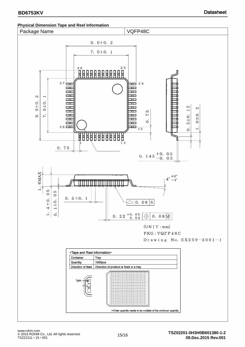
Package W(Typ) x D(Typ) x H(Max) VQFP48C 9.00mm x 9.00mm x 1.60mm
VQFP48C
Datasheet
Datasheet
2/16
TSZ02201-0H3H0B601380-1-2 © 2015 ROHM Co., Ltd. All rights reserved. www.rohm.com
TSZ22111・15・001
BD6753KV
09.Dec.2015 Rev.001
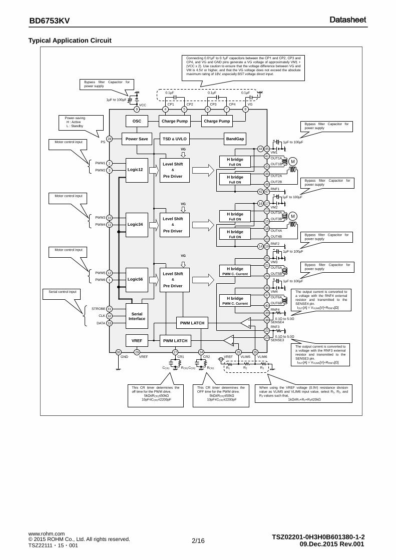
Typical Application Circuit
Bypass filter Capacitor for
power supply
Bypass filter Capacitor for
power supply
Bypass filter Capacitor for
power supply
Bypass filter Capacitor for
power supply
Bypass filter Capacitor for
power supply
Power-saving
H : Active
L : Standby
Motor control input
Motor control input
Motor control input
Serial control input The output current is converted to
a voltage with the RNF4 external
resistor and transmitted to the
SENSE4 pin. IOUT[A] = VVLIM6[V]÷RRNF4[Ω]
When using the VREF voltage (0.9V) resistance division
value as VLIM5 and VLIM6 input value, select R1, R2, and
R3 values such that, 1kΩ≤R1+R2+R3≤20kΩ
This CR timer determines the
OFF time for the PWM drive.
5kΩ≤RCR2≤50kΩ 10pF≤CCR2≤2200pF
This CR timer determines the
off time for the PWM drive.
5kΩ≤RCR1≤50kΩ 10pF≤CCR1≤2200pF
Connecting 0.01μF to 0.1μF capacitors between the CP1 and CP2, CP3 and
CP4, and VG and GND pins generate a VG voltage of approximately VM1 +
(VCC x 2). Use caution to ensure that the voltage difference between VG and
VM is 4.5V or higher, and that the VG voltage does not exceed the absolute maximum rating of 18V, especially BST voltage direct input.
The output current is converted to
a voltage with the RNF3 external
resistor and transmitted to the
SENSE3 pin. IOUT[A] = VVLIM5[V]÷RRNF3[Ω]
VCC
1µF to 100µF
OUT1A
OUT1B Level Shift
&
Pre Driver
OUT2A
OUT2B
H bridge
Full ON
H bridge
Full ON
M
CLK
STROBE
DATA
BandGap TSD & UVLO
33
32
31
9
41
43
46
48
1µF to 100µF
VM1 45
RNF1 47
OUT3A
OUT3B Level Shift
&
Pre Driver
OUT4A
OUT4B
H bridge
Full ON
H bridge
Full ON
M
13
15
18
20
17
RNF2 19
VM2
Charge Pump Charge Pump
CP1
4
CP2
5
CP3
6
CP4
7
VG
8
OUT5A
OUT5B
21
24
1µF to 100µF
25
RNF4
0.1Ω to 5.0Ω
OUT6B
H bridge
PWM C. Current
37
40
39
VM3
Level Shift
&
Pre Driver 36
VM4
OUT6A
SENSE4 38
RNF3
0.1Ω to 5.0Ω
22
SENSE3 23
H bridge
PWM C. Current
C.
VREF PWM LATCH
PWM LATCH
0.1μF 0.1μF
VG
VG
VG
Lo
gic
45
PS
PWM1
28 Power Save
PWM2
2
3
PWM4
10
11
PWM3
PWM6
12
1
PWM5
Logic56
Logic12
Logic34
Serial Interface
44
42
16
14
30 29 34
R2 R3 R1
VLIM5 VLIM6
26 35 27
RCR2 CCR2 RCR1 CCR1
VREF CR2 CR1 GND VREF
0.1μF
OSC
1µF to 100µF
1µF to 100µF

3/16
TSZ02201-0H3H0B601380-1-2 © 2015 ROHM Co., Ltd. All rights reserved. www.rohm.com
TSZ22111・15・001
BD6753KV
09.Dec.2015 Rev.001
Pin Configurations
Pin Descriptions
Pin No. Pin Name Function Pin No. Pin Name Function
1 PWM6 PWM control logic input 6 25 VM3 Motor power supply ch.5
2 PWM1 PWM control logic input 1 26 VLIM5 Output current setting ch.5
3 PWM2 PWM control logic input 2 27 CR1 CR timer setting ch.5
4 CP1 1st Bucket stage with capacitor 1 28 PS Power-saving
5 CP2 1st Bucket stage with capacitor 2 29 VREF Reference voltage output
6 CP3 2nd Bucket stage with capacitor 3 30 GND Ground
7 CP4 2nd Bucket stage with capacitor 4 31 STROBE Serial enable input
8 VG Charge pump output with capacitor 32 CLK Serial clock input
9 VCC Power supply 33 DATA Serial data input
10 PWM3 PWM control logic input 3 34 CR2 CR timer setting ch.6
11 PWM4 PWM control logic input 4 35 VLIM6 Output current setting ch.6
12 PWM5 PWM control logic input 5 36 VM4 Motor power supply ch.6
13 OUT3A H-bridge output 3A 37 OUT6A H-bridge output 6A
14 RNF2 Motor ground ch.3, ch.4 38 SENSE4 Output current detection ch.6
15 OUT3B H-bridge output 3B 39 RNF4 Current detect resistor ch.6
16 VM2 Motor power supply ch.3, ch.4 40 OUT6B H-bridge output 6B
17 VM2 Motor power supply ch.3, ch.4 41 OUT1A H-bridge output 1A
18 OUT4A H-bridge output 4A 42 RNF1 Motor ground ch.1, ch.2
19 RNF2 Motor ground ch.3, ch.4 43 OUT1B H-bridge output 1B
20 OUT4B H-bridge output 4B 44 VM1 Motor power supply ch.1, ch.2
21 OUT5A H-bridge output 5A 45 VM1 Motor power supply ch.1, ch.2
22 RNF3 Current detect resistor ch.5 46 OUT2A H-bridge output 2A
23 SENSE3 Output current detection ch.5 47 RNF1 Motor ground ch.1, ch.2
24 OUT5B H-bridge output 5B 48 OUT2B H-bridge output 2B
BD6753KV
48
36
12
24 OUT6A
SENSE4
RNF4
OUT6B
OUT1A
RNF1
OUT1B
VM1
VM1
OUT2A
RNF1
OUT2B
OUT5B
SENSE3
RNF3
OUT5A
OUT4B
RNF2
OUT4A
VM2
VM2
OUT3B
RNF2
OUT3A
VM
4
VLIM
6
CR
2
DA
TA
CLK
ST
RO
BE
GN
D
VR
EF
PS
CR
1
VLIM
5
VM
3
PW
M6
PW
M1
PW
M2
CP
1
CP
2
CP
3
CP
4
VG
VC
C
PW
M3
PW
M4
PW
M5
(TOP VIEW)

4/16
TSZ02201-0H3H0B601380-1-2 © 2015 ROHM Co., Ltd. All rights reserved. www.rohm.com
TSZ22111・15・001
BD6753KV
09.Dec.2015 Rev.001
Block Diagram
Description of Blocks
1. Power-Saving Function A power-saving function is included, which allows the system to save power when not driving the motor. The voltage level on this pin should be set high so as to keep the operation mode. (See the Electrical Characteristics; p.7/16)
2. Motor Control Input
(a) PWM1 to PWM6 Pins Logic level controls the output logic of H-Bridge. (See the Electrical Characteristics; p.7/16, and I/O Truth Table; p.9/16)
(b) Serial Interface
It is possible to set the logic as EN/IN mode or IN/IN via serial interface.
(See the Electrical Characteristics; p.7/16 and I/O Truth Table; p.9/16)
3. H-bridge Each H-bridge can be controlled independently. It is therefore possible to drive the H-bridges simultaneously, as long as the package thermal tolerances are not exceeded. Because the output transistors consist of power DMOS that can be controlled the charge pump output VG, the total ON-Resistance of high and low-side transistor is dependent on VG voltage VG. Further, the whole application must be designed so that the maximum current of each channel may be 500mA or below. (See the Recommended Operating Conditions; p.6/16)
VCC
OUT1A
OUT1B Level Shift
&
Pre Driver
OUT2A
OUT2B
H bridge
Full ON
H bridge
Full ON
CLK
STROBE
DATA
BandGap TSD & UVLO
33
32
31
9
41
43
46
48
VM1 45
RNF1 47
OUT3A
OUT3B Level Shift
&
Pre Driver
OUT4A
OUT4B
H bridge
Full ON
H bridge
Full ON
13
15
18
20
17
RNF2 19
VM2
Charge Pump Charge Pump
CP1
4
CP2
5
CP3
6
CP4
7
VG
8
OUT5A
OUT5B
21
24
25
RNF4
OUT6B
H bridge
PWM C. Current
37
40
39
VM3
Level Shift
&
Pre Driver 36 VM4
OUT6A
SENSE4 38
RNF3 22
SENSE3 23
H bridge
PWM C. Current
C.
VREF PWM LATCH
PWM LATCH
VG
VG
VG
Lo
gic
45
PS
PWM1
28 Power Save
PWM2
2
3
PWM4
10
11
PWM3
PWM6
12
1
PWM5
Logic56
Logic12
Logic34
Serial Interface
44
42
16
14
30 29 34
VLIM5 VLIM6
26 35 27
CR2 CR1 GND VREF
OSC

5/16
TSZ02201-0H3H0B601380-1-2 © 2015 ROHM Co., Ltd. All rights reserved. www.rohm.com
TSZ22111・15・001
BD6753KV
09.Dec.2015 Rev.001
Description of Blocks – continued
4. Drive System of PWM Constant-Current H-bridge (Channel 5, Channel 6)
(a) Output Current Detection & Current Settings
A low-value (0.1Ω to 5.0Ω) resistor can be placed between the RNF3 or RNF4 pins and ground to detect the
motor winding current. When making the RNF3 and SENSE3 pins or RNF4 and SENSE4 short-circuit, the internal
circuits can output the accurate constant current by comparing the external voltage of VLIM5 or VLIM6 pin with
detecting voltage. The internal reference voltage (VREF pin: 0.9V±10%) can be divided using external resistors
(1kΩ to 20kΩ). The resulting value can be input as the set voltage. It is also necessary to connect a resistor and
capacitor to the CR1 and CR2 pins in order to determine the PWM drive OFF time.
(b) PWM Constant-Current Control Operation
The motor current rises through the winding at a rate dependent upon the voltage and inductance of the winding. If the RNF3 or RNF4 voltage reaches the threshold voltage set with the VLIM5 or VLIM6 voltage, the internal current limiting comparator changes the logic of H-Bridges into short brake mode. Because both of low-side DMOS transistors are on, the motor’s inductance causes the current to freewheel through them. During this freewheeling time, the current decreases until the CR timer reaches constant OFF time (tOFF). After this sequence, the high-side DMOS transistor is enabled to increase the winding current again. For repeating this cycle, the motor winding current will be regulated by the motor’s inductance.
(c) Noise Cancellation Function The device has a noise cancellation time (Tn) to blank detection of the motor winding current. A noise cancellation time blanks the output of the current limiting comparator when the output transistors are switched. The noise cancellation time defines the minimum on time for PWM constant current, and it depends on the internal resistor, external resistor and capacitor of CR pin.
(d) CR Timer
The moment output logic are switched to short brake mode, the voltage of CR pin is clamped at approximately
0.9V. Because the external capacitor discharges toward ground through the external resistor during the short
brake mode, the voltage of CR pin decreases until approximately 0.4V. That time defines the OFF time (tOFF). As
soon as the voltage of CR pin reaches 0.4V, the external capacitor charges toward VCC voltage. That cycle
continues to repeat with the capacitor alternately charging and discharging. The interval over which the capacitor
charges from 0.4V to approximately 0.8V defines the noise cancellation time (Tn). The tOFF and Tn depend upon
the external resistor and capacitor values connected to the CR pin. Because a low-value resistor will prevent the
voltage of CR pin from reaching the clamp voltage, select within the range of 5kΩ to 50kΩ. The capacitor values
should be set within the range of 10pF to 2200pF. The use of a capacitor in excess of 2200pF will lengthen the
noise cancellation time and control the output current unstably. Setting a longer OFF time may reduce both the
average current and the motor rotational efficiency to increase the ripple of motor winding current.
Output Current Value IOUT[A] = VVLIM5[V] / RRNF3[Ω] or VVLIM6[V] / RRNF4[Ω]
Figure 1. Peak Current Control PWM Constant-Current Drive with the CR Timer
Output current: IOUT[A]
RNF voltage: VRNF[V]
CR voltage: VCR[V]
PWM Constant-Current
setting value
0V
VLIM pin setting voltage
0.9V
0.8V
0.4V
Noise cancellation time: Tn[sec]
Charge period
Discharge period
Off time: tOFF[sec]
Spike noise 0A

6/16
TSZ02201-0H3H0B601380-1-2 © 2015 ROHM Co., Ltd. All rights reserved. www.rohm.com
TSZ22111・15・001
BD6753KV
09.Dec.2015 Rev.001
Description of Blocks – continued
If the VLIM5 or VLIM6 pin is shorted to the VCC pin (or the same voltage as the VCC is set) and the SENSE3 pin or SENSE4 and RNF3 pin or RNF4 are shorted to the ground, these channels can drive as a Full-ON type H-bridge like other channels.
5. Charge Pump
Because the respective output transistors consist of power N-channel DMOS, the gate voltage VG should be higher than the VM voltage to drive the high-side N-channel DMOS. The device includes the charge pump circuit that generates VG voltage by connecting three external capacitors. The approximately (VM1 + (VCC x 2)) voltage is output on the VG pin in the state with which a capacitor (0.1μF) is connected respectively between CP1 pin and CP2, CP3 and CP4, VG and GND. The charge pump's output voltage is approximately (VM1 + VCC) voltage when connecting a capacitor (0.1μF) respectively between CP1 and CP2 pin, VG and GND pin, in addition to be shorted CP4 pin and VG, and to be open CP3 pin. It is possible to set the different voltages to each VM pin (VM1 to VM4). In order to provide better performance, the voltage difference between VG and VM must be 4.5V or above, and the VG voltage must not exceed the absolute maximum rating of 18V.
Absolute Maximum Ratings (Ta=25°C)
Parameter Symbol Limit Unit
Power Supply Voltage VCC -0.5 to +7.0 V
Motor Power Supply Voltage VM -0.5 to +12.5 V
Charge Pump Voltage VG 18.0 V
Control Input Voltage VIN -0.5 to +VCC+0.5 V
Power Dissipation Pd 1.12 (Note 1) W
H-bridge Output Current IOUT -0.8 to +0.8 (Note 2) A/ch
Storage Temperature Range Tstg -55 to +150 °C
Junction Temperature Tjmax 150 °C
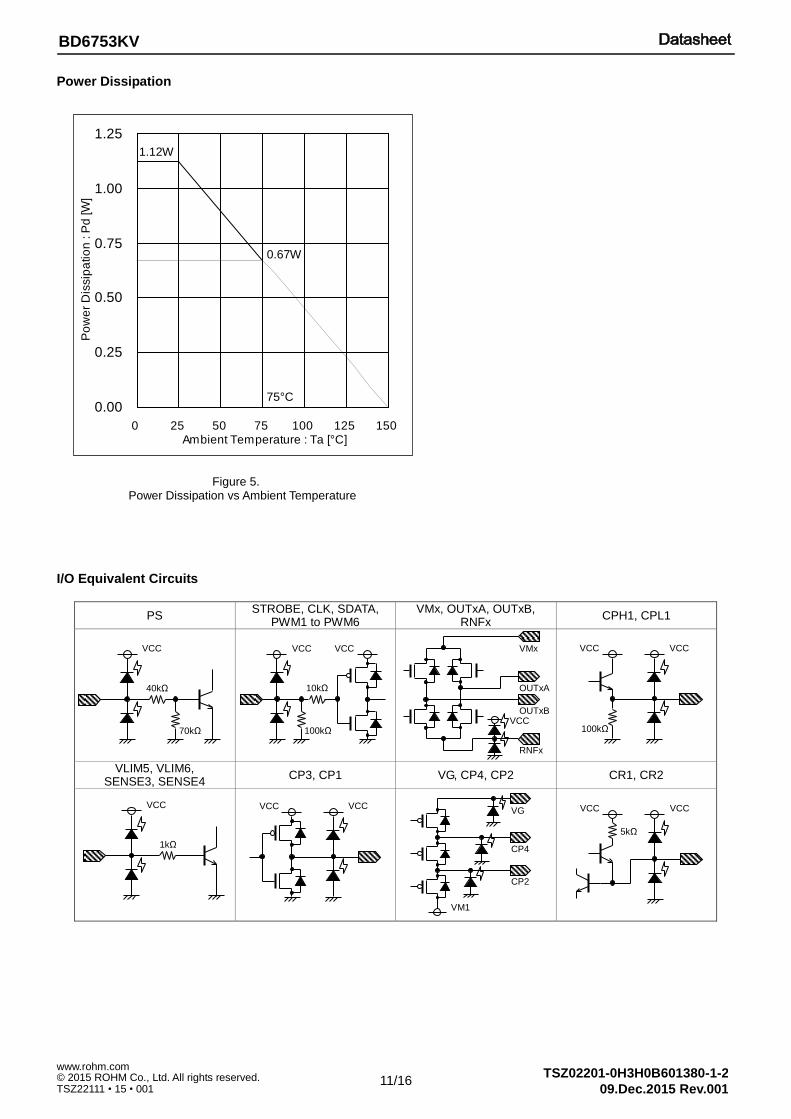
(Note 1) Reduced by 9.0mW/°C over 25°C, when mounted on a glass epoxy board (70mm x 70mm x 1.6mm) (Note 2) Must not exceed Pd, ASO, or Tjmax of 150°C Caution: Operating the IC over the absolute maximum ratings may damage the IC. The damage can either be a short circuit between pins or an open circuit between pins and the internal circuitry. Therefore, it is important to consider circuit protection measures, such as adding a fuse, in case the IC is operated over the absolute maximum ratings.
Recommended Operating Conditions
Parameter Symbol Min Typ Max Unit
Power Supply Voltage VCC 2.7 - 5.5 V
Motor Power Supply Voltage(VM1) VM1 4.5 - 10.5 V
Motor Power Supply Voltage(VM2 to VM4) VM2 to VM4 2.0 - 10.5 V
Control Input Voltage VIN 0 - VCC V
H-bridge Output Current(Note 3) IOUT -0.5 - +0.5 A/ch
Output Current Control Voltage Range VLIM 0 - 0.5 V
PWM Signal Input Frequency fPWM 0 - 0.1 MHz
Operating Temperature Range Topr -25 - +75 °C
(Note 3) Must not exceed Pd, ASO, or Tjmax of 150°C

7/16
TSZ02201-0H3H0B601380-1-2 © 2015 ROHM Co., Ltd. All rights reserved. www.rohm.com
TSZ22111・15・001
BD6753KV
09.Dec.2015 Rev.001
Electrical Characteristics (Unless otherwise specified VCC=3.3V, VM=10.5V, Ta=25°C)
Parameter Symbol Min Typ Max Unit Conditions
All Circuits
Stand-By Current ICCST - 0 10 μA VPS=0V
Circuit Current ICC - 2.2 3.0 mA VPS=3.3V with no signal, CRx open
Power-Saving (PS)
High-Level Input Voltage VPSH 2.0 - VCC V
Low-Level Input Voltage VPSL 0 - 0.7 V
High-Level Input Current IPSH 25 50 100 μA VPS=3.3V
Low-Level Input Current IPSL -1 0 - μA VPS=0V
Control Input (IN=STROBE, CLK, DATA, PWM1 to PWM6)
High-Level Input Voltage VINH 2.0 - VCC V
Low-Level Input Voltage VINL 0 - 0.7 V
High-Level Input Current IINH 16.5 33 66 μA VIN=3.3V
Low-Level Input Current IINL -1 0 - μA VIN=0V
Pull-down Resistor RIN 50 100 200 kΩ
Charge Pump
Charge Pump Voltage VCP 16 16.5 - V
Under Voltage Locked Out (UVLO)
UVLO Voltage VUVLO 1.6 - 2.5 V
Full-ON Drive Block (Channel 1 to Channel 4)
Output ON-Resistance RON - 1.2 1.5 Ω IOUT=±400mA, VG=16.5V, total
PWM Linear Constant-Current Drive Block (Channel 5, Channel 6)
Output ON-Resistance RON - 1.2 1.5 Ω IOUT=±400mA, VG=16.5V, total
VLIM Input Current IVLIM -1 -0.2 - μA VLIMx=0V, VSENSEx=0.5V
SENSE Input Current ISENSE -1 -0.2 - μA VLIMx=0.5V, VSENSEx=0V
Output Limit Voltage VOL 485 500 515 mV VLIMx=500mV
CR Clamp Voltage VCR 0.8 0.9 1.0 V R=10kΩ
CR Switching High Voltage VCRH 0.72 0.80 0.88 V
CR Switching Low Voltage VCRL 0.36 0.40 0.44 V
Minimum ON Time tMINON 0.1 0.5 1.0 μs C=470pF, R=10kΩ
Constant Voltage Power Supply
VREF Output Voltage VREF 0.81 0.90 0.99 V IOUT=0mA to 1mA

8/16
TSZ02201-0H3H0B601380-1-2 © 2015 ROHM Co., Ltd. All rights reserved. 09.Dec.2015 Rev.001
www.rohm.com
TSZ22111 • 15 • 001
BD6753KV
Typical Performance Curves
Figure 2.
Circuit Current vs Supply Voltage
Figure 3.
Output ON-Resistance vs Charge Pump Voltage (VM=10.5V)
0.0
1.0
2.0
3.0
4.0
5.0
0.0 1.0 2.0 3.0 4.0 5.0 6.0 7.0Power Supply Voltage : VCC [V]
Cir
cu
it C
urr
en
t : I C
C [m
A]
Top 75°C Mid 25°C Low -25°C
Operating range
(2.7V to 5.5V)
0.0
1.0
2.0
3.0
4.0
5.0
13.0 14.0 15.0 16.0 17.0 18.0Charge Pump Voltage : VG [V]
Ou
tpu
t O
n R
esis
tan
ce
: R
ON [Ω
]
Top 75°C Mid 25°C Low -25°C

9/16
TSZ02201-0H3H0B601380-1-2 © 2015 ROHM Co., Ltd. All rights reserved. 09.Dec.2015 Rev.001
www.rohm.com
TSZ22111 • 15 • 001
BD6753KV
Timing chart
Table 1. I/O Truth Table
Input Mode
INPUT OUTPUT
Serial data Pin
modx pxa pxb PWMx OUTxA OUTxB Output Mode(Note 4)
IN/IN L
L L X Z Z OPEN
L H L L H CCW
L H H L L Short Brake
H L L H L CW
H L H L L Short Brake
H H X L L Short Brake
EN/IN H
L X X Z Z OPEN
H L L H L CW
H L H L H CCW
H H X L L Short Brake L: Low, H: High, X: Don’t care, Z: Hi impedance
(Note 4) CW: Current flows from OUTxA to OUTxB, CCW: Current flows from OUTxB to OUTxA (x=1 to 6)
Table 2. Serial Resistor Bit Map
No. ADDRESS BIT DATA BIT
Bit[7] Bit[6] Bit[5] Bit[4] Bit[3] Bit[2] Bit[1] Bit[0]
00H 0 0 mod2 mod1 p2a p2b p1a p1b
01H 0 1 mod4 mod3 p4a p4b p3a p3b
02H 1 0 mod6 mod5 p6a p6b p5a p5b
The device provides 8-bit and 3-line serial interface in order to set output logic modes. The DATA is sent to the internal shift register during the STROBE logic low interval at the CLK rising edge. Shift register data is written to the internal 6-bit memory simultaneously with STROBE rising edge, according to the addresses stored in Bit[7] and Bit[6]. The serial data input order is Bit[0] to Bit[7]. The stand-by condition is cleared all serial data, and also the UVLO fault condition.
Figure 4. Serial Input Sequence
STROBE
CLK
DATA Bit[0] Bit[1] Bit[2] Bit[3] Bit[4] Bit[5] Bit[6] Bit[7] Bit[0] Bit[1] Bit[5] Bit[6] Bit[7]
100%
0%
100%
0%
100%
0%
DATA BITS ADDRESS BITS
Timing of input serial data writing to internal register
ADDRESS BITS
Timing of register data writing
to internal memory
DATA BITS
10/16
TSZ02201-0H3H0B601380-1-2 © 2015 ROHM Co., Ltd. All rights reserved. 09.Dec.2015 Rev.001
www.rohm.com
TSZ22111 • 15 • 001
BD6753KV
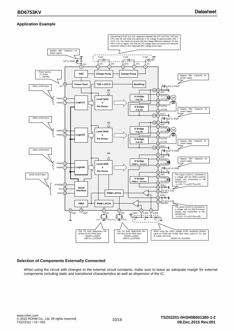
Application Example
Selection of Components Externally Connected
When using the circuit with changes to the external circuit constants, make sure to leave an adequate margin for external components including static and transitional characteristics as well as dispersion of the IC.
Bypass filter Capacitor for
power supply
Bypass filter Capacitor for
power supply
Bypass filter Capacitor for
power supply
Bypass filter Capacitor for
power supply
Bypass filter Capacitor for
power supply
Power-saving
H : Active
L : Standby
Motor control input
Motor control input
Motor control input
Serial control input The output current is converted to
a voltage with the RNF4 external
resistor and transmitted to the
SENSE4 pin. IOUT[A] = VVLIM6[V]÷RRNF4[Ω]
When using the VREF voltage (0.9V) resistance division
value as VLIM5 and VLIM6 input value, select R1, R2, and
R3 values such that, 1kΩ≤R1+R2+R3≤20kΩ
This CR timer determines the
OFF time for the PWM drive.
5kΩ≤RCR2≤50kΩ 10pF≤CCR2≤2200pF
This CR timer determines the
off time for the PWM drive.
5kΩ≤RCR1≤50kΩ 10pF≤CCR1≤2200pF
Connecting 0.01μF to 0.1μF capacitors between the CP1 and CP2, CP3 and
CP4, and VG and GND pins generate a VG voltage of approximately VM1 +
(VCC x 2). Use caution to ensure that the voltage difference between VG and
VM is 4.5V or higher, and that the VG voltage does not exceed the absolute maximum rating of 18V, especially BST voltage direct input.
The output current is converted to
a voltage with the RNF3 external
resistor and transmitted to the
SENSE3 pin. IOUT[A] = VVLIM5[V]÷RRNF3[Ω]
VCC
1µF to 100µF
OUT1A
OUT1B Level Shift
&
Pre Driver
OUT2A
OUT2B
H bridge
Full ON
H bridge
Full ON
M
CLK
STROBE
DATA
BandGap TSD & UVLO
33
32
31
9
41
43
46
48
1µF to 100µF
VM1 45
RNF1 47
OUT3A
OUT3B Level Shift
&
Pre Driver
OUT4A
OUT4B
H bridge
Full ON
H bridge
Full ON
M
13
15
18
20
17
RNF2 19
VM2
Charge Pump Charge Pump
CP1
4
CP2
5
CP3
6
CP4
7
VG
8
OUT5A
OUT5B
21
24
1µF to 100µF
25
RNF4
0.1Ω to 5.0Ω
OUT6B
H bridge
PWM C. Current
37
40
39
VM3
Level Shift
&
Pre Driver 36
VM4
OUT6A
SENSE4 38
RNF3
0.1Ω to 5.0Ω
22
SENSE3 23
H bridge
PWM C. Current
C.
VREF PWM LATCH
PWM LATCH
0.1μF 0.1μF
VG
VG
VG
Lo
gic
45
PS
PWM1
28 Power Save
PWM2
2
3
PWM4
10
11
PWM3
PWM6
12
1
PWM5
Logic56
Logic12
Logic34
Serial Interface
44
42
16
14
30 29 34
R2 R3 R1
VLIM5 VLIM6
26 35 27
RCR2 CCR2 RCR1 CCR1
VREF CR2 CR1 GND VREF
0.1μF
OSC
1µF to 100µF
1µF to 100µF
11/16
TSZ02201-0H3H0B601380-1-2 © 2015 ROHM Co., Ltd. All rights reserved. 09.Dec.2015 Rev.001
www.rohm.com
TSZ22111 • 15 • 001
BD6753KV
Power Dissipation
Figure 5. Power Dissipation vs Ambient Temperature
I/O Equivalent Circuits
PS STROBE, CLK, SDATA,
PWM1 to PWM6 VMx, OUTxA, OUTxB,
RNFx CPH1, CPL1
VLIM5, VLIM6, SENSE3, SENSE4
CP3, CP1 VG, CP4, CP2 CR1, CR2
0.00
0.25
0.50
0.75
1.00
1.25
0 25 50 75 100 125 150Ambient Temperature : Ta [°C]
Po
we
r D
issip
atio
n : P
d [W
]
1.12W
0.67W
75°C
VCC
70kΩ
40kΩ
VCC
10kΩ
VCC
100kΩ
OUTxA
RNFx
VMx
OUTxB VCC
VCC VCC
100kΩ
VCC
1kΩ
VCC VCC
CP4
CP2
VG
VM1
VCC VCC
5kΩ

12/16
TSZ02201-0H3H0B601380-1-2 © 2015 ROHM Co., Ltd. All rights reserved. 09.Dec.2015 Rev.001
www.rohm.com
TSZ22111 • 15 • 001
BD6753KV
Operational Notes
1. Reverse Connection of Power Supply
Connecting the power supply in reverse polarity can damage the IC. Take precautions against reverse polarity when connecting the power supply, such as mounting an external diode between the power supply and the IC’s power supply pins.
2. Power Supply Lines
Design the PCB layout pattern to provide low impedance supply lines. Separate the ground and supply lines of the digital and analog blocks to prevent noise in the ground and supply lines of the digital block from affecting the analog block. Furthermore, connect a capacitor to ground at all power supply pins. Consider the effect of temperature and aging on the capacitance value when using electrolytic capacitors.
3. Ground Voltage
Ensure that no pins are at a voltage below that of the ground pin at any time, even during transient condition.
4. Ground Wiring Pattern
When using both small-signal(GND) and large-current ground(RNF) traces, the two ground traces should be routed separately but connected to a single ground at the reference point of the application board to avoid fluctuations in the small-signal ground caused by large currents. Also ensure that the ground traces of external components do not cause variations on the ground voltage. The ground lines must be as short and thick as possible to reduce line impedance.
5. Thermal Consideration
Should by any chance the power dissipation rating be exceeded the rise in temperature of the chip may result in deterioration of the properties of the chip. In case of exceeding this absolute maximum rating, increase the board size and copper area to prevent exceeding the Pd rating.
6. Recommended Operating Conditions
These conditions represent a range within which the expected characteristics of the IC can be approximately obtained. The electrical characteristics are guaranteed under the conditions of each parameter.
7. Inrush Current
When power is first supplied to the IC, it is possible that the internal logic may be unstable and inrush current may flow instantaneously due to the internal powering sequence and delays, especially if the IC has more than one power supply. Therefore, give special consideration to power coupling capacitance, power wiring, width of ground wiring, and routing of connections.
8. Operation Under Strong Electromagnetic Field
Operating the IC in the presence of a strong electromagnetic field may cause the IC to malfunction.
9. Testing on Application Boards
When testing the IC on an application board, connecting a capacitor directly to a low-impedance output pin may subject the IC to stress. Always discharge capacitors completely after each process or step. The IC’s power supply should always be turned off completely before connecting or removing it from the test setup during the inspection process. To prevent damage from static discharge, ground the IC during assembly and use similar precautions during transport and storage.
10. Inter-pin Short and Mounting Errors
Ensure that the direction and position are correct when mounting the IC on the PCB. Incorrect mounting may result in damaging the IC. Avoid nearby pins being shorted to each other especially to ground, power supply and output pin. Inter-pin shorts could be due to many reasons such as metal particles, water droplets (in very humid environment) and unintentional solder bridge deposited in between pins during assembly to name a few.
11. Unused Input Pins
Input pins of an IC are often connected to the gate of a MOS transistor. The gate has extremely high impedance and extremely low capacitance. If left unconnected, the electric field from the outside can easily charge it. The small charge acquired in this way is enough to produce a significant effect on the conduction through the transistor and cause unexpected operation of the IC. So unless otherwise specified, unused input pins should be connected to the power supply or ground line.
13/16
TSZ02201-0H3H0B601380-1-2 © 2015 ROHM Co., Ltd. All rights reserved. 09.Dec.2015 Rev.001
www.rohm.com
TSZ22111 • 15 • 001
BD6753KV
Operational Notes – continued
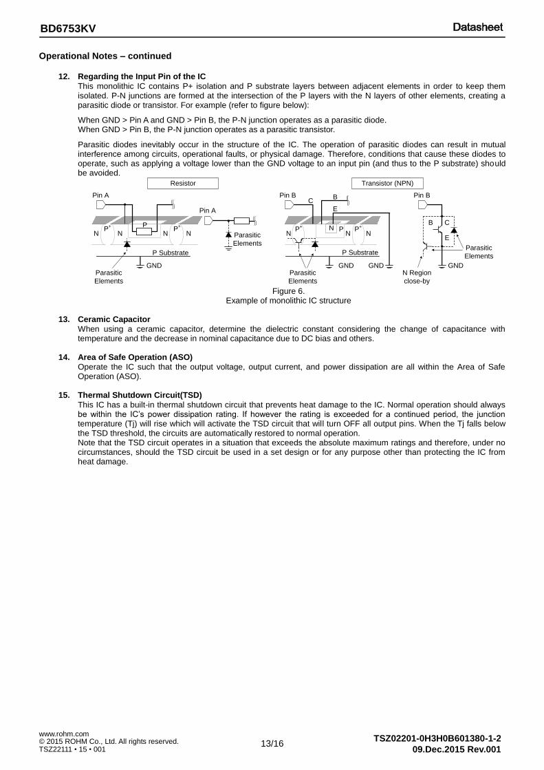
12. Regarding the Input Pin of the IC
This monolithic IC contains P+ isolation and P substrate layers between adjacent elements in order to keep them isolated. P-N junctions are formed at the intersection of the P layers with the N layers of other elements, creating a parasitic diode or transistor. For example (refer to figure below):
When GND > Pin A and GND > Pin B, the P-N junction operates as a parasitic diode. When GND > Pin B, the P-N junction operates as a parasitic transistor.
Parasitic diodes inevitably occur in the structure of the IC. The operation of parasitic diodes can result in mutual interference among circuits, operational faults, or physical damage. Therefore, conditions that cause these diodes to operate, such as applying a voltage lower than the GND voltage to an input pin (and thus to the P substrate) should be avoided.
Figure 6. Example of monolithic IC structure
13. Ceramic Capacitor
When using a ceramic capacitor, determine the dielectric constant considering the change of capacitance with temperature and the decrease in nominal capacitance due to DC bias and others.
14. Area of Safe Operation (ASO)
Operate the IC such that the output voltage, output current, and power dissipation are all within the Area of Safe Operation (ASO).
15. Thermal Shutdown Circuit(TSD)
This IC has a built-in thermal shutdown circuit that prevents heat damage to the IC. Normal operation should always be within the IC’s power dissipation rating. If however the rating is exceeded for a continued period, the junction temperature (Tj) will rise which will activate the TSD circuit that will turn OFF all output pins. When the Tj falls below the TSD threshold, the circuits are automatically restored to normal operation. Note that the TSD circuit operates in a situation that exceeds the absolute maximum ratings and therefore, under no circumstances, should the TSD circuit be used in a set design or for any purpose other than protecting the IC from heat damage.
N NP
+ P
N NP
+
P Substrate
GND
NP
+
N NP
+N P
P Substrate
GND GND
Parasitic
Elements
Pin A
Pin A
Pin B Pin B
B C
E
Parasitic
Elements
GNDParasitic
Elements
CB
E
Transistor (NPN)Resistor
N Region
close-by
Parasitic
Elements

14/16
TSZ02201-0H3H0B601380-1-2 © 2015 ROHM Co., Ltd. All rights reserved. 09.Dec.2015 Rev.001
www.rohm.com
TSZ22111 • 15 • 001
BD6753KV
Ordering Information
B D 6 7 5 3 K V -
Part Number
Package KV : VQFP48C
Packaging and forming specification None: Tray
Marking Diagram
Part Number Marking Package Orderable Part Number
BD6753KV VQFP48C BD6753KV
VQFP48C (TOP VIEW)
BD6753KV
Part Number Marking
LOT Number
1PIN MARK
15/16
TSZ02201-0H3H0B601380-1-2 © 2015 ROHM Co., Ltd. All rights reserved. 09.Dec.2015 Rev.001
www.rohm.com
TSZ22111 • 15 • 001
BD6753KV
Physical Dimension Tape and Reel Information
Package Name VQFP48C

16/16
TSZ02201-0H3H0B601380-1-2 © 2015 ROHM Co., Ltd. All rights reserved. 09.Dec.2015 Rev.001
www.rohm.com
TSZ22111 • 15 • 001
BD6753KV
Revision History
Date Revision Changes
09.Dec.2015 001 New Release
DatasheetDatasheet
Notice-PGA-E Rev.002© 2015 ROHM Co., Ltd. All rights reserved.
Notice Precaution on using ROHM Products
1. Our Products are designed and manufactured for application in ordinary electronic equipments (such as AV equipment, OA equipment, telecommunication equipment, home electronic appliances, amusement equipment, etc.). If you intend to use our Products in devices requiring extremely high reliability (such as medical equipment (Note 1), transport equipment, traffic equipment, aircraft/spacecraft, nuclear power controllers, fuel controllers, car equipment including car accessories, safety devices, etc.) and whose malfunction or failure may cause loss of human life, bodily injury or serious damage to property (“Specific Applications”), please consult with the ROHM sales representative in advance. Unless otherwise agreed in writing by ROHM in advance, ROHM shall not be in any way responsible or liable for any damages, expenses or losses incurred by you or third parties arising from the use of any ROHM’s Products for Specific Applications.
(Note1) Medical Equipment Classification of the Specific Applications JAPAN USA EU CHINA
CLASSⅢ CLASSⅢ
CLASSⅡb CLASSⅢ
CLASSⅣ CLASSⅢ
2. ROHM designs and manufactures its Products subject to strict quality control system. However, semiconductor
products can fail or malfunction at a certain rate. Please be sure to implement, at your own responsibilities, adequate safety measures including but not limited to fail-safe design against the physical injury, damage to any property, which a failure or malfunction of our Products may cause. The following are examples of safety measures:
[a] Installation of protection circuits or other protective devices to improve system safety [b] Installation of redundant circuits to reduce the impact of single or multiple circuit failure
3. Our Products are designed and manufactured for use under standard conditions and not under any special or extraordinary environments or conditions, as exemplified below. Accordingly, ROHM shall not be in any way responsible or liable for any damages, expenses or losses arising from the use of any ROHM’s Products under any special or extraordinary environments or conditions. If you intend to use our Products under any special or extraordinary environments or conditions (as exemplified below), your independent verification and confirmation of product performance, reliability, etc, prior to use, must be necessary:
[a] Use of our Products in any types of liquid, including water, oils, chemicals, and organic solvents [b] Use of our Products outdoors or in places where the Products are exposed to direct sunlight or dust [c] Use of our Products in places where the Products are exposed to sea wind or corrosive gases, including Cl2,
H2S, NH3, SO2, and NO2
[d] Use of our Products in places where the Products are exposed to static electricity or electromagnetic waves [e] Use of our Products in proximity to heat-producing components, plastic cords, or other flammable items [f] Sealing or coating our Products with resin or other coating materials [g] Use of our Products without cleaning residue of flux (even if you use no-clean type fluxes, cleaning residue of
flux is recommended); or Washing our Products by using water or water-soluble cleaning agents for cleaning residue after soldering
[h] Use of the Products in places subject to dew condensation
4. The Products are not subject to radiation-proof design. 5. Please verify and confirm characteristics of the final or mounted products in using the Products. 6. In particular, if a transient load (a large amount of load applied in a short period of time, such as pulse. is applied,
confirmation of performance characteristics after on-board mounting is strongly recommended. Avoid applying power exceeding normal rated power; exceeding the power rating under steady-state loading condition may negatively affect product performance and reliability.
7. De-rate Power Dissipation depending on ambient temperature. When used in sealed area, confirm that it is the use in
the range that does not exceed the maximum junction temperature. 8. Confirm that operation temperature is within the specified range described in the product specification. 9. ROHM shall not be in any way responsible or liable for failure induced under deviant condition from what is defined in
this document.
Precaution for Mounting / Circuit board design 1. When a highly active halogenous (chlorine, bromine, etc.) flux is used, the residue of flux may negatively affect product
performance and reliability.
2. In principle, the reflow soldering method must be used on a surface-mount products, the flow soldering method must be used on a through hole mount products. If the flow soldering method is preferred on a surface-mount products, please consult with the ROHM representative in advance.
For details, please refer to ROHM Mounting specification

DatasheetDatasheet
Notice-PGA-E Rev.002© 2015 ROHM Co., Ltd. All rights reserved.
Precautions Regarding Application Examples and External Circuits 1. If change is made to the constant of an external circuit, please allow a sufficient margin considering variations of the
characteristics of the Products and external components, including transient characteristics, as well as static characteristics.
2. You agree that application notes, reference designs, and associated data and information contained in this document
are presented only as guidance for Products use. Therefore, in case you use such information, you are solely responsible for it and you must exercise your own independent verification and judgment in the use of such information contained in this document. ROHM shall not be in any way responsible or liable for any damages, expenses or losses incurred by you or third parties arising from the use of such information.
Precaution for Electrostatic
This Product is electrostatic sensitive product, which may be damaged due to electrostatic discharge. Please take proper caution in your manufacturing process and storage so that voltage exceeding the Products maximum rating will not be applied to Products. Please take special care under dry condition (e.g. Grounding of human body / equipment / solder iron, isolation from charged objects, setting of Ionizer, friction prevention and temperature / humidity control).
Precaution for Storage / Transportation 1. Product performance and soldered connections may deteriorate if the Products are stored in the places where:
[a] the Products are exposed to sea winds or corrosive gases, including Cl2, H2S, NH3, SO2, and NO2 [b] the temperature or humidity exceeds those recommended by ROHM [c] the Products are exposed to direct sunshine or condensation [d] the Products are exposed to high Electrostatic
2. Even under ROHM recommended storage condition, solderability of products out of recommended storage time period may be degraded. It is strongly recommended to confirm solderability before using Products of which storage time is exceeding the recommended storage time period.
3. Store / transport cartons in the correct direction, which is indicated on a carton with a symbol. Otherwise bent leads
may occur due to excessive stress applied when dropping of a carton. 4. Use Products within the specified time after opening a humidity barrier bag. Baking is required before using Products of
which storage time is exceeding the recommended storage time period.
Precaution for Product Label QR code printed on ROHM Products label is for ROHM’s internal use only.
Precaution for Disposition When disposing Products please dispose them properly using an authorized industry waste company.
Precaution for Foreign Exchange and Foreign Trade act Since concerned goods might be fallen under listed items of export control prescribed by Foreign exchange and Foreign trade act, please consult with ROHM in case of export.
Precaution Regarding Intellectual Property Rights 1. All information and data including but not limited to application example contained in this document is for reference
only. ROHM does not warrant that foregoing information or data will not infringe any intellectual property rights or any other rights of any third party regarding such information or data.
2. ROHM shall not have any obligations where the claims, actions or demands arising from the combination of the Products with other articles such as components, circuits, systems or external equipment (including software).
3. No license, expressly or implied, is granted hereby under any intellectual property rights or other rights of ROHM or any third parties with respect to the Products or the information contained in this document. Provided, however, that ROHM will not assert its intellectual property rights or other rights against you or your customers to the extent necessary to manufacture or sell products containing the Products, subject to the terms and conditions herein.
Other Precaution 1. This document may not be reprinted or reproduced, in whole or in part, without prior written consent of ROHM.
2. The Products may not be disassembled, converted, modified, reproduced or otherwise changed without prior written consent of ROHM.
3. In no event shall you use in any way whatsoever the Products and the related technical information contained in the Products or this document for any military purposes, including but not limited to, the development of mass-destruction weapons.
4. The proper names of companies or products described in this document are trademarks or registered trademarks of ROHM, its affiliated companies or third parties.

DatasheetDatasheet
Notice – WE Rev.001© 2015 ROHM Co., Ltd. All rights reserved.
General Precaution 1. Before you use our Pro ducts, you are requested to care fully read this document and fully understand its contents.
ROHM shall n ot be in an y way responsible or liabl e for fa ilure, malfunction or acci dent arising from the use of a ny ROHM’s Products against warning, caution or note contained in this document.
2. All information contained in this docume nt is current as of the issuing date and subj ect to change without any prior
notice. Before purchasing or using ROHM’s Products, please confirm the la test information with a ROHM sale s representative.
3. The information contained in this doc ument is provi ded on an “as is” basis and ROHM does not warrant that all
information contained in this document is accurate an d/or error-free. ROHM shall not be in an y way responsible or liable for any damages, expenses or losses incurred by you or third parties resulting from inaccuracy or errors of or concerning such information.

Mouser Electronics
Authorized Distributor
Click to View Pricing, Inventory, Delivery & Lifecycle Information: ROHM Semiconductor:
BD6753KV