mpc18730, power management ic with five … · 41 vo2_sense_in input voltage input power switch 2...
TRANSCRIPT

Document Number: MPC18730Rev. 4.0, 8/2006
Freescale Semiconductor Advance Information
Power Management IC with Five Regulated Outputs Programmed Through 3-Wire Serial Interface
The MPC18730 Power Management IC (PMIC) regulates five independent output voltages from either a single cell Li-Ion (2.7 V to 4.2 V input range) or from a single cell Ni-MH or dry cell (0.9 V to 2.2 V input range).
The PMIC includes 2 DC-DC converters and 3 low drop out (LDO) linear regulators. The output voltage for each of the 5 output voltages is set independently through a 3-wire serial interface. The serial interface also configures the PMIC's versatile start-up control system, which includes multiple wakeup, sleep, standby, and reset modes to minimize power consumption for portable equipment.
In single cell Li-Ion applications two DC-DC converters are configured as buck (step-down) regulators. In single cell Ni-MH or dry cell applications, one DC-DC converter is configured as a boost (step-up) regulator, and the other as buck-boost regulator. The DC-DC converters' output voltages have set ranges 1.613 V to 3.2 V at up to 120 mA, and 0.805 V to 1.5 V up to 100 mA.
Features• Operates from single cell Li-Ion, Ni-MH, or Alkaline• 2 DC-DC Converters• 3 Low Drop Regulators• Serial Interface Sets Output Voltages• 4 Wake Inputs• Low Current Standby Mode• Pb-Free Packaging Designated by Suffix Code EP
Figure 1. MPC18730 Simplified Application Diagram
POWER MANAGEMENT IC
EP SUFFIX (PB-FREE)98ARL10571D
64-PIN QFN
18730
ORDERING INFORMATION
Device Temperature Range (TA) Package
MPC18730EP/R2 -10°C to 65°C 64 QFN
MPC18730
VBATT
VREF
VB
VO
PGOOD1
CONTROL
LOGIC
INPUTS
GND
GNDGATE
VOUT1
SW1
VOUT2
VO2_SENSE
SW2
SREGO1
SREGO2
SREGO3
VGATE
SWGATE
VB
SREGI1
SREGI2
SREGI3
VGATE_EXT
1.613 V to 3.2 V
0.865 V to 2.8 V
0.011 V to 2.8 V
2.08 V to 2.8 V
Programmable
0.805 V to 1.5 VProgrammable
Programmable
Programmable
ProgrammableMCU
PGOOD2
VO
VO1_SENSE
* This document contains certain information on a new product. Specifications and information herein are subject to change without notice.
© Freescale Semiconductor, Inc., 2006. All rights reserved.

INTERNAL BLOCK DIAGRAM
INTERNAL BLOCK DIAGRAM
Figure 2. MPC18730 Simplified Internal Block Diagram
VGATE_EXT
VREF
EAIN1
EAOUT1
DMAX1
PGND1
VIN1
VOUT1
SW2
V_STDBY
LVB
HVB
EAOUT2
EAIN2
DMAX2
PGOOD2_DELAY
PGND2
VIN2
VOUT2
VO2_SENSE_IN
DATASTRB
VGATE
SREGO1SREGC1
SREGC2
SREGC3
GNDGATE
SREGI1
WATCHDOG
GND
SEQ_SELECT CH_PUMP
SREGO2
SREGO3
SREGI3
CLEAR
VO1_SENSE
BANDGAP
VO1_SENSE
VO1_SENSE
VBATT
VGATE
POWERSWITCH1
LVB
PGOOD1(Int)PGOOD1(Int)
PGOOD1(Int)
Driver
REFERENCE
VO1_SENSE
Step-UpDownDC/DC
VMODE
PGOOD1(Int)
VREF
POWERSWITCH2
REF2
PGOOD2(Int)VGATE
Step-UpDownDC/DC
PGOOD2(Int)
CONTROL
VO1_SENSEVBATT
Series Pass
VGATE
VGATEVBATT
VREF
Regulator1
Series Pass
VGATE
VBATT
REF3
REF4
REF5
SEQ_SELECT
EXT_CLOCK
REF1
REF2
REF3
REF4
REF5
REF DAC
VMODE
Series Pass
VGATE
Regulator3
Regulator2
CPoff
VGATE_DUTY
VG_SELECT
VGATE
HG
LG
SREGI2
SWGATE
OnEXT gate
On
EXT_CLOCK
CLEAR
SCKIN
WAKE1BWAKE2BWAKE3BWAKE4B
RESET1_TH
PGOOD1
LSWO
SLEEP
PGOOD1_DELAY
Buffer
SREG2G
ControlLogic
Step-UpDC/DC
Convertor
Converter
RESETBlock 2
VO1_SENSE
RESETBlock 1
PGOOD2
PGOOD1(Int)
CH1
ConverterCH2
V_STDBY
(Int)
VGATE
PGOOD2
SREGC1
VGATESEL1VGATESEL2
VBATT
VO2_SENSE
VO1_SENSE
SW1
VGATE
VO1_SENSE
REF1
Analog Integrated Circuit Device Data 2 Freescale Semiconductor
18730

PIN CONNECTIONS
PIN CONNECTIONS
Figure 3. MPC18730 Pin Connections
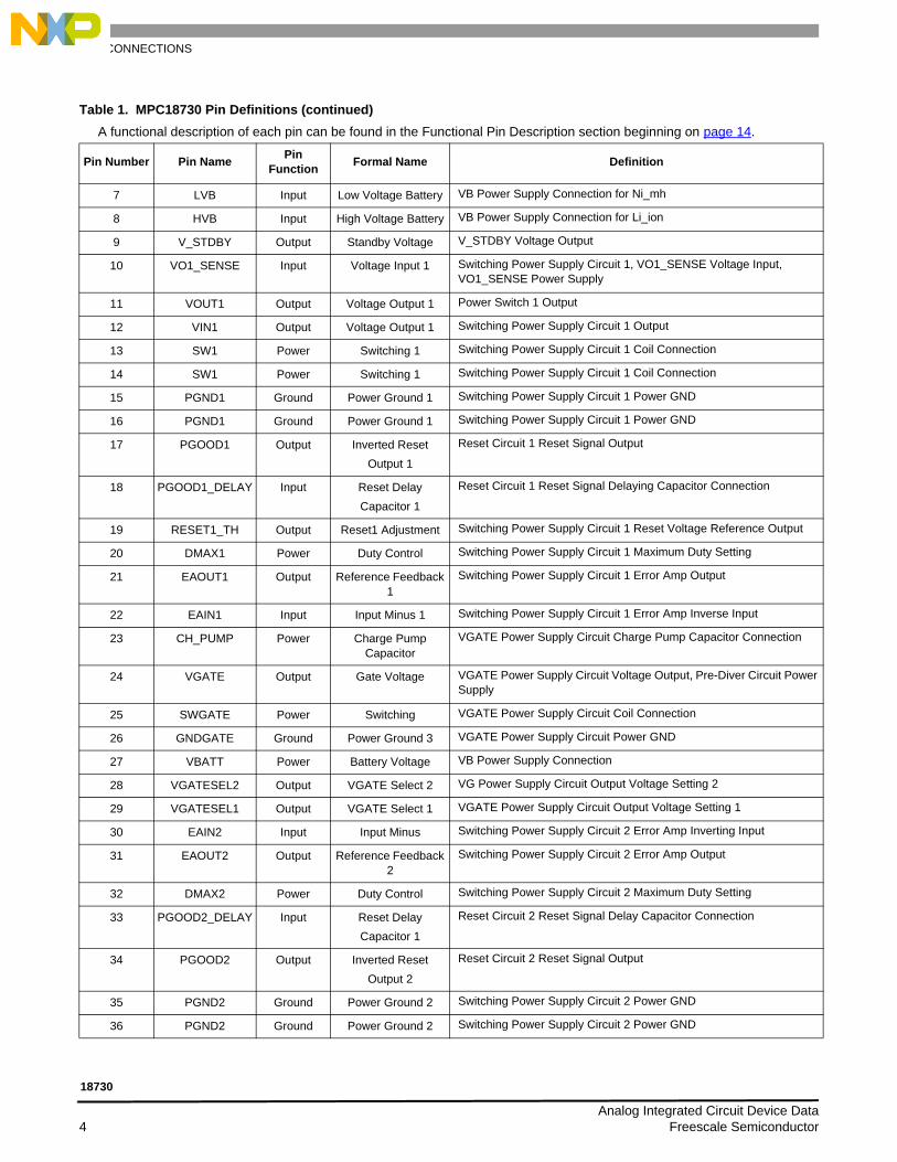
Table 1. MPC18730 Pin Definitions A functional description of each pin can be found in the Functional Pin Description section beginning on page 14.
Pin Number Pin Name Pin Function Formal Name Definition
1 CLEAR Input Clear Start-up Signal Input Latch/Clear
2 WAKE4B Input Wake Signal 4 Start-up Signal Input 4
3 WAKE3B Input Wake Signal 3 Start-up Signal Input 3
4 WAKE2B Input Wake Signal 2 Start-up Signal Input 2
5 WAKE1B Input Wake Signal 1 Start-up Signal Input 1
6 LSWO Output Low-Side Switch Output
Low-Side Switch Output Pin
2
3
4
5
6
7
8
9
10
11
12
13
14
15
1619 20 21 22 23 24 25 26 27 28 29 30 31 32
48
47
46
45
44
43
42
41
40
39
38
37
36
35
34
64 63 62 61 60 59 58 57 56 55 54 53 52 51 50
TOP VIEW
CLEAR
WAKE4B
WAKE3B
WAKE2B
WAKE1B
LSWO
LVB
HVB
V_STDBY
VO1_SENSE
VOUT1
VIN1
SW1
SW1
PGND1
PGND1
PG
OO
D1
PG
OO
D1_
DE
LAY
EA
OU
T1
EA
IN1
CH
_PU
MP
VG
ATE
GN
DG
ATE
VB
AT
T
EA
IN2
PGOOD2_DELAY
PGOOD2
PGND2
SW2
SW2
VIN2
VOUT2
VO2_SENSE_IN
SREGO3
SREGI3
SR
EG
O2
VO2_SENSE
SR
EG
O1
SR
EG
I1
SR
EG
C1
SREGC2
SREGC3
GN
D
SR
EG
2G
VG
AT
ES
EL2
LG
VR
EF
DM
AX
1
HGD
ATA
STR
B
SC
KIN
WA
TCH
DO
G
1 49
331718
VGATE_EXT
SR
EG
I2
PGND2
SE
Q_S
ELE
CT
VG
ATE
SE
L1
DM
AX
2
SWG
ATE
RE
SE
T1_T
H
SLE
EP
EX
T_C
LOC
K
EAO
UT2
Analog Integrated Circuit Device Data Freescale Semiconductor 3
18730
PIN CONNECTIONS
7 LVB Input Low Voltage Battery VB Power Supply Connection for Ni_mh
8 HVB Input High Voltage Battery VB Power Supply Connection for Li_ion
9 V_STDBY Output Standby Voltage V_STDBY Voltage Output
10 VO1_SENSE Input Voltage Input 1 Switching Power Supply Circuit 1, VO1_SENSE Voltage Input, VO1_SENSE Power Supply
11 VOUT1 Output Voltage Output 1 Power Switch 1 Output
12 VIN1 Output Voltage Output 1 Switching Power Supply Circuit 1 Output
13 SW1 Power Switching 1 Switching Power Supply Circuit 1 Coil Connection
14 SW1 Power Switching 1 Switching Power Supply Circuit 1 Coil Connection
15 PGND1 Ground Power Ground 1 Switching Power Supply Circuit 1 Power GND
16 PGND1 Ground Power Ground 1 Switching Power Supply Circuit 1 Power GND
17 PGOOD1 Output Inverted ResetOutput 1
Reset Circuit 1 Reset Signal Output
18 PGOOD1_DELAY Input Reset DelayCapacitor 1
Reset Circuit 1 Reset Signal Delaying Capacitor Connection
19 RESET1_TH Output Reset1 Adjustment Switching Power Supply Circuit 1 Reset Voltage Reference Output
20 DMAX1 Power Duty Control Switching Power Supply Circuit 1 Maximum Duty Setting
21 EAOUT1 Output Reference Feedback 1
Switching Power Supply Circuit 1 Error Amp Output
22 EAIN1 Input Input Minus 1 Switching Power Supply Circuit 1 Error Amp Inverse Input
23 CH_PUMP Power Charge Pump Capacitor
VGATE Power Supply Circuit Charge Pump Capacitor Connection
24 VGATE Output Gate Voltage VGATE Power Supply Circuit Voltage Output, Pre-Diver Circuit Power Supply
25 SWGATE Power Switching VGATE Power Supply Circuit Coil Connection
26 GNDGATE Ground Power Ground 3 VGATE Power Supply Circuit Power GND
27 VBATT Power Battery Voltage VB Power Supply Connection
28 VGATESEL2 Output VGATE Select 2 VG Power Supply Circuit Output Voltage Setting 2
29 VGATESEL1 Output VGATE Select 1 VGATE Power Supply Circuit Output Voltage Setting 1
30 EAIN2 Input Input Minus Switching Power Supply Circuit 2 Error Amp Inverting Input
31 EAOUT2 Output Reference Feedback 2
Switching Power Supply Circuit 2 Error Amp Output
32 DMAX2 Power Duty Control Switching Power Supply Circuit 2 Maximum Duty Setting
33 PGOOD2_DELAY Input Reset DelayCapacitor 1
Reset Circuit 2 Reset Signal Delay Capacitor Connection
34 PGOOD2 Output Inverted ResetOutput 2
Reset Circuit 2 Reset Signal Output
35 PGND2 Ground Power Ground 2 Switching Power Supply Circuit 2 Power GND
36 PGND2 Ground Power Ground 2 Switching Power Supply Circuit 2 Power GND
Table 1. MPC18730 Pin Definitions (continued)A functional description of each pin can be found in the Functional Pin Description section beginning on page 14.
Pin Number Pin Name Pin Function Formal Name Definition
Analog Integrated Circuit Device Data 4 Freescale Semiconductor
18730

PIN CONNECTIONS
37 SW2 Power Switching Switching Power Supply Circuit 2 Coil Connection
38 SW2 Power Switching Switching Power Supply Circuit 2 Coil Connection
39 VIN2 Output Voltage Output Switching Power Supply Circuit 2 Output
40 VOUT2 Output Voltage Output Power Switch 2 Output
41 VO2_SENSE_IN Input Voltage Input Power Switch 2 Voltage Input
42 VO2_SENSE Input Voltage Input Switching Power Supply Circuit 2 VO2_SENSE Voltage Input
43 HG Output Step Down Top FET 2 Switching Power Supply Circuit 2 Step down Top side FET Gate Output for Ni_mh
44 LG Output Step Down Bottom FET 2
Switching Power Supply Circuit 2 Step down Bottom side FRT Gate Output for Ni_mh
45 VGATE_EXT Output Gate Switch External Transistor Gate Signal Output
46 SREGC3 Power Regulator Capacitor 3 Series Pass Power Supply Circuit 3 External Feedback Connection
47 SREGO3 Output Regulator Output 3 Series Pass Power Supply Circuit 3 Output
48 SREGI3 Power Regulator Input 3 Series Pass Power Supply Circuit 3 Power Supply
49 SREGC2 Power Regulator Capacitor 2 Series Pass Power Supply Circuit 2 External Feedback Connection
50 SREG2G Output Regulator Gate Output 2
Series Pass Power Supply Circuit 2 External Transistor Gate Signal Output
51 SREGO2 Output Regulator Output 2 Series Pass Power Supply Circuit 2 Output
52 SREGI2 Power Regulator Input 2 Series Pass Power Supply Circuit 2 Power Supply
53 SREGC1 Power Regulator Capacitor 1 Series Pass Power Supply Circuit 1 External Feedback Connection
54 SREGO1 Output Regulator Output 1 Series Pass Power Supply Circuit 1 Output
55 SREGI1 Power Regulator Input 1 Series Pass Power Supply Circuit 1 Power Supply
56 GND Ground Ground GND
57 VREF Output Reference Voltage Reference Voltage Output
58 DATA Input Data Signal Serial Interface Data Signal Input
59 STRB Input Strobe Serial Interface Strobe Signal Input
60 SCKIN Input Serial Clock Serial Interface Clock Signal Input
61 WATCHDOG Input Watch Dog Timer Watchdog Timer Capacitor Connection
62 SEQ_SELECT Input Sequence Input Start-Up Sequence Setting Input
63 EXT_CLOCK Input Clock Input External Synchronous Clock Signal Input
64 SLEEP Input Sleep Signal Sleep Signal Input
Table 1. MPC18730 Pin Definitions (continued)A functional description of each pin can be found in the Functional Pin Description section beginning on page 14.
Pin Number Pin Name Pin Function Formal Name Definition
Analog Integrated Circuit Device Data Freescale Semiconductor 5
18730

ELECTRICAL CHARACTERISTICSMAXIMUM RATINGS
ELECTRICAL CHARACTERISTICS
MAXIMUM RATINGS
Table 2. Maximum Ratings
All voltages are with respect to ground unless otherwise noted. Exceeding these ratings may cause a malfunction or permanent damage to the device.
Ratings Symbol Value Unit
ELECTRICAL RATINGS
Power Supply Voltage VBATT -0.5 to 5.0 V
Analog Signal Input (1) VINAN -0.5 to VO1+0.5 V
Logic Signal InputWAKE1~4BCLEAR, SLEEP, EXT_CLOCK, SCKIN, DATA, STRBVGATESEL1,2
VILRSTB
VILGC
VILGSEL
-0.5 to V_STDBY+0.5-0.5 to VO1_SENSE+0.5
-0.5 to VBATT+0.5
V
Output Power Current
VOUT1 Power Supply Circuit (2)
VOUT2 Power Supply CircuitSREG1 Power Supply CircuitSREG2 Power Supply CircuitSREG3 Power Supply CircuitVGATE Power Supply CircuitPGOOD1 Power Supply Circuit
IOVO1
IOVO2
IOREG1
IOREG2
IOREG3
IOVG
IOPGOOD1
12010080
100808
-20
mA
Open-Drain Output Apply VoltagePGOOD1LSWO
VIODR
VIODV
-0.5 to 3.3-0.5 to 3.3
V
ESD Voltage (3)
Human Body Model (HBM)Machine Model (MM)Charge Device Model (CDM)
VESD1VESD2VCDM
± 1500± 200± 750
V
THERMAL RATINGS
Operating TemperatureAmbientJunction
TATJ
-10 to 65150
°C
Storage Temperature TSTG -50 to 150 °C
Thermal Resistance (4)
Junction to Ambient RθJA 69 °C/W
Lead Soldering Temperature(5) TSOLDER 260 °C
Notes1. VREF, DMAX1, DMAX2, SREGC1, SREGC2, SREGC3 and RESET1_TH.2. Includes the series pass power supply circuit output current3. ESD testing is performed in accordance with the Human Body Model (HBM) (CZAP = 100 pF, RZAP = 1500 Ω), the Machine Model (MM)
(CZAP = 200 pF, RZAP = 0 Ω), and the Charge Device Model (CDM), Robotic (CZAP = 4.0pF).4. Device mounted on a 2s2p test board, in accordance with JEDEC JESD51-6 and JESD51-7.5. Pin soldering temperature limit is for 10 seconds maximum duration. Not designed for immersion soldering. Exceeding these limits may
cause malfunction or permanent damage to the device.
Analog Integrated Circuit Device Data 6 Freescale Semiconductor
18730

ELECTRICAL CHARACTERISTICSSTATIC
STATIC
Table 3. Static Electrical Characteristics Characteristics noted under conditions VBATT = 1.2 V, VO1_SENSE = 2.4 V, VGATE= 6.0 V, fCLK = 176.4 kHz unless
otherwise noted. Typical values noted reflect the approximate parameter means at TA = 27°C under nominal conditions unless otherwise noted.
Characteristic Symbol Min Typ Max Unit
GENERAL
VB Power Supply VoltagePower Supply Voltage 1Power Supply Voltage 2
VLVB
VHVB
0.92.7
1.23.5
2.24.2
V
Series Regulator Input Voltage (6), (7) VSREGI VSREG+0.2(8) VSREG+0.3 VSREG+0.4 V
Start-Up Voltage VBST 0.9 - - V
Analog Signal Input (9) VIANA 0 - VO1_SENSE V
Logic Signal InputWAKE1~4BCLEAR, SLEEP, EXT_CLOCK, DATA, STRB and SCKINVGATESEL1, 2
VILRSTB
VILGC
VILGSEL
000
---
V_STDBYVO1_SENSE
VBATT
V
Output Power Current
VOUT1 Power Supply Circuit (10)
VOUT2 Power Supply Circuit (10)
SREG1 Power Supply CircuitSREG2 Power Supply CircuitSREG3 Power Supply CircuitVGATE Power Supply CircuitPGOOD
IOVOUT1
IOVOUT2
IOSREG1
IOSREG2
IOSREG3
IOVG
IOPGOOD
00
5.06.05.0-5.0
-
-------
100806080606.00
mA
Supply Current in Stand-by modeVB Supply Current (VB = 1.2 V for Ni_MH)(HVB = 3.5 V for Li-Ion)
IBSNi
IBSLi
--
5.08.0
1012
µA
Supply Current in Operating modeVB Supply Current (VB = 1.2 V for Ni_MH)(HVB = 3.5 V for Li-Ion)
IBNi
IBLi
--
9.07.0
1814
mA
Reference Power Supply CircuitOutput VoltageOutput Current
VREF
IOREF
1.255-0.3
1.275-
1.2950.3
VmA
Switching Power Supply 1VOUT1 Output Voltage (Io = 0~100 mA)
VOUT1 2.3 2.4 2.5 V
Notes6. When applying voltage from an external source.7. 0.3 V when VGATE is 4.5 V.8. Provide 2 V or higher for the voltage difference (VGATE - VO1_SENSE).9. VREF, DMAX1, DMAX2, SREGC1, SREGC2, SREGC3 and RESET1_TH.
10. Includes the series pass power supply circuit output current.
Analog Integrated Circuit Device Data Freescale Semiconductor 7
18730

ELECTRICAL CHARACTERISTICSSTATIC
Switching Power Supply 2VOUT2 Output Voltage (Io = 0~80 mA)
HG Output Voltage (11) (Isource = 400 µA)
(Isink = 400 µA)
LG Output Voltage (11) (Isource = 400 µA)
(Isink = 400 µA)
VOUT2
VDW2TH
VDW2TL
VDW2BH
VDW2BL
1.055.20
5.20
1.15----
1.25VGATE
0.3VGATE
0.3
V
Series Pass Power Supply Circuit
SREG1 Control Voltage (Io = 5~60 mA) (12)
SREG1-Error AMP Input offset voltage (13)
SREG2 Control Voltage (Io = 6~80 mA) (12)
SREG2-Error AMP Input offset voltage (14)
SREG3 Control Voltage (Io = 5~60 mA) (12)
SREG3-Error AMP Input offset voltage (15)
SREG2G Output Voltage (16) (Isource = 2.5 µA)
(Isink = 2.5 µA)
VSREG1
SR1OFSTVSREG2
SR2OFSTVSREG3
SR3OFSTSREG2GHSREG2GL
2.7-13.52.7-172.7-115.00
2.8-
2.8-
2.8---
2.924.52.9172.923
VGATE0.5
VmVV
mVV
mVVV
Power Switch On ResistanceVOUT1 CircuitVOUT2 Circuit
RVOUT1
RVOUT2
--
0.40.4
0.60.6
W
VGATE Power Supply Circuit
(Io = 0~6 mA) (17)
(Io = 0~6 mA) (18)
CH_PUMP Output Voltage (Isource = 2.5 mA)
(Isink = 2.5 mA)
VGH Voltage (Certified value)
VGATE_00
VGATE_10
VO1_SENSE1LH
VO1_SENSE_1LL
VGH
5.54.6
VB x 0.850-
6.05.0---
6.55.4VB0.4
10.5
V
V_STDBY Output Voltage for Li_ion (Io = 300 µA) (19) VLVB 1.75 - 2.45 V
Notes11. Connect a transistor with gate capacity of 200 pF or smaller to HG and LG12. If a capacitor with capacitance of 22 µF is connected to SREGO, use a phase compensation capacitor between SREGO and SREGC
when the load is 5 mA (6 mA for SREG2) or lower. The output voltage values shown in the table assume that external resistance is connected as follows: SREGI1 = 3.0 V to 3.3 V, 65.14KΩ between SREGO1 and SREGC1, 34.86KΩ between SREGC1 and GND. SREGI2 = 3.0 V to 3.3 V, 54.46KΩ between SREGO2 and SREGC2, 45.54KΩ between SREGC2 and GND. SREGI3 = 3.0 V to 3.3 V, 73.84KΩ between SREGO3 and SREGC3, 26.16KΩ between SREGC3 and GND.
13. Calculated by the right formula for input offset: SR1OFST = (Vref x 0.77) - (SREGO1 ÷ (100k ÷ 34.86k))14. Calculated by the right formula for input offset: SR2OFST = (Vref x 1) - (SREGO1 ÷ (100k ÷ 45.54k))15. Calculated by the right formula for input offset: SR3OFST = (Vref x 0.58) - (SREGO1 ÷ (100k ÷ 26.16k))16. Connect a transistor with gate capacity of 300 pF or smaller to REG2G.17. When VGATESEL1 is Low and VGATESEL2 is Low, I/O = 3 mA or higher is certified by specification.18. When VGATESEL1 is High and VGATESEL2 is Low, I/O = 3 mA or higher is certified by specification.19. When HVB is 4.2 V and the load from V_STDBY is 0.5 µA or higher.
Table 3. Static Electrical Characteristics (continued)Characteristics noted under conditions VBATT = 1.2 V, VO1_SENSE = 2.4 V, VGATE= 6.0 V, fCLK = 176.4 kHz unless
otherwise noted. Typical values noted reflect the approximate parameter means at TA = 27°C under nominal conditions unless otherwise noted.
Characteristic Symbol Min Typ Max Unit
Analog Integrated Circuit Device Data 8 Freescale Semiconductor
18730

ELECTRICAL CHARACTERISTICSSTATIC
Reset CircuitReset Voltage 1
Reset Voltage 2
Hysteresis Voltage 1 (@RST1)Hysteresis Voltage 2 (@RST2)PGOOD (VPGOOD = 2.4 V)
(Isink = 2 mA)
PGOOD_DELAY (Isink = 100 µA)
High Level Threshold VoltageLow Level Threshold VoltagePGOOD_DELAY Pull-Up Resistance
VRST1
VRST2
VHYRS1
VHYRS2
IPGOOD1,2
VPGOOD1,2
VOLCR1,2
VIHCR1,2
VILCR1,2
RPUPRC1,2
0.85 x VO1_SENSE
0.80 x VO1_SENSE
4050000
1.250.7550
0.88 x VO1_SENSE
0.85 x VO1_SENSE
7875---
1.421.00100
0.91 x VO1_SENSE
0.90 x VO1_SENSE
115100100.50.7
1.651.15150
V
V
mVmVµAVVVV
KΩ
V_STDBY Output ResistanceOutput Resistance (VO1_SENSE)Output Resistance (VBATT)
RVO1_SENSE
RVB
--
30200
45400
W
LSWO Output ResistanceOutput Resistance
RLSWO - 42 50 W
VGATE_EXTVGATE_EXT Output Voltage (Isource = 100 µA)
(Isink = 100 µA)VOHEXTG
VOLEXTG
VGATE x 0.90
--
VGATEVGATE x 0.1
V
Logic Input
"H" Level Input Voltage (20)
"L" Level Input Voltage (20)
"H" Level Input Voltage (21)
"L" Level Input Voltage (21)
"H" Level Input Voltage (22)
"L" Level Input Voltage (22)
"H" Level Input Current (20), (22)
"L" Level Input Current (22), (23)
Pull Up Resistance (24)
Pull Down Resistance (25)
VIHVS
VILVS
VIH
VIL
VIHVB
VILVB
IIHIIL
RPUP
RPDW
V_STDBY - 0.2-
1.5-
VB - 0.2-
-1.0-1.0410330
--------
590480
-0.2-
0.4-
0.21.01.0770625
VVVVVV
µAµAKΩ
KΩ
Notes20. Applied to WAKEB1 ~ 4 and SEQ_SELECT.21. Applied to CLEAR, SLEEP, EXT_CLOCK, DATA, STRB and SCKIN.22. Applied to VGATESEL1 and 2.23. Applied to WAKEB1 ~ 3, CLEAR, SLEEP, EXT_CLOCK, DATA, STRB, SCKIN and SEQ_SELECT.24. Applied to WAKEB4.25. Applied to CLEAR, SLEEP, EXT_CLOCK, DATA, STRB and SCKIN.
Table 3. Static Electrical Characteristics (continued)Characteristics noted under conditions VBATT = 1.2 V, VO1_SENSE = 2.4 V, VGATE= 6.0 V, fCLK = 176.4 kHz unless
otherwise noted. Typical values noted reflect the approximate parameter means at TA = 27°C under nominal conditions unless otherwise noted.
Characteristic Symbol Min Typ Max Unit
Analog Integrated Circuit Device Data Freescale Semiconductor 9
18730

ELECTRICAL CHARACTERISTICSDYNAMIC
DYNAMIC
Table 4. Dynamic Electrical Characteristics
Characteristics noted under conditions VBATT = 1.2 V, VO1_SENSE = 2.4 V, VGATE = 6.0 V, fCLK = 176.4 kHz unless otherwise noted. Typical values noted reflect the approximate parameter means at TA = 27°C under nominal conditions unless otherwise noted.
Characteristic Symbol Min Typ Max Unit
OSCILLATOR
Internal Oscillation Frequency fICK 150 200 250 kHz
MICRO CONTROLLER INTERFACE
Clock Signal Input (26) fCLK - 176.4 - kHz
Serial Interface (Refer to Figure 5, Serial Interface Timing Diagrams)DATA Set Up TimeDATA Hold TimeSCKIN Clock FrequencySCKIN 'H' Pulse WidthSCKIN 'L' Pulse WidthSCKIN Hold TimeSTRB Set Up TimeSTRB Pulse Width
tsth
fsck
twckh
twckl
thck
tssb
twsb
2020-
5050505050
--
6.0-----
--------
nsecnsecMHznsecnsecnsecnsecnsec
Notes26. Duty 50%.
Analog Integrated Circuit Device Data 10 Freescale Semiconductor
18730

ELECTRICAL CHARACTERISTICSTIMING DIAGRAMS
TIMING DIAGRAMS
Figure 4. Power Supply Start-Up Timing Diagram
WAKE1~4(int)
EXT_CLOCK
V_STDBY
VBATT
VGATE
PGOOD1(Int)
PGOOD1
VO1_SENSE
VOUT1
VO2_SENSE
VOUT2
SREG1~3
DATA
STRB
CLEAR
SLEEP
VBATT
VBATT
VBATTVO1_SENSE
VGATE
VBATT
VO1_SENSE
VO2_SENSE
VBATT
VBATT
INT EXT
VO1_SENSE
VO1_SENSE
VO2_SENSE
DATA
PGOOD1
VO1_SENSEPGOOD2(Int)
Standby Mode*1: When using Ni_mh. High-Z when using Li_ion.
Start-Up
(Serial setting)
PGOOD_DELAY set value
PGOOD_DELAY set value
SEQ_SELECT setting
SEQ_SELECT setting
Operation Mode Standby Mode
VO1_SENSE
VO1_SENSE
VBATT
Analog Integrated Circuit Device Data Freescale Semiconductor 11
18730

ELECTRICAL CHARACTERISTICSTIMING DIAGRAMS
Figure 5. Serial Interface Timing Diagrams
Twelve bits immediately before start-up of STRB are always effective. Upon power on, the internal power on reset works to initialize the registers. Serial data is fetched in the
order of Add_[3], Add_[2], ..., Add_[0], DATA1_[3], DATA1_[2], ...., DATA2_[0].
Table 5. Serial Interface Functions
Register Name Address DATA1 DATA2
0 CLEAR, SLEEP 1000 CLEAR SLEEP Reserved Reserved Reserved Reserved Reserved Reserved
1 Power Mode 0001 PSW1 PSW2 PGOOD1 VOUT2 SREG1 SREG2 SREG3 PGOOD2
2 Clock Select 0010 Ext / Int Half Freq RSTB sleep S_Off_VGATE VG_Duty[3] VG_Duty[2] VG_Duty[1] VG_Duty[0]
3 VO1_SENSE 0011 MSB VO1_SENSE Output Voltage LSB S_Off_VO1_SENSE
4 VO2_SENSE 0100 MSB VO2_SENSE Output Voltage LSB S_Off_VO2_SENSE
5 SREG1 0101 MSB SREG1 Output Voltage LSB Reserved
6 SREG2 0110 MSB SREG2 Output Voltage LSB
7 SREG3 0111 MSB SREG3 Output Voltage LSB CP Off EXTG On
SCKIN
DATA
STRB
tS tH
tSSB tWCKH tWCKL tHCK
A3 D0
tWSB
A2
Table 6. Block Operation
INPUT OUTPUT
WAKE(Int)
PGOOD1(Int) PGOOD1 PGOOD2(Int) SEQ_SELECT VGATE VO1_SENSE VO2_SENSE VOUT1,2 REG
1,2,3
L X X X X - - - - -
H L L L L O O - - -
H H L L L O O - - O
H H L L H O O - - -
H H H H L O O O O O
H H H H H O O O O O
O : Operation, - : Stop, X : Don’t care
Analog Integrated Circuit Device Data 12 Freescale Semiconductor
18730

ELECTRICAL CHARACTERISTICSTIMING DIAGRAMS
Table 7. Start-Up Sequence Settings
SEQ_SELECT
CLEAR/SLEEP Series Regulators
V_STDBY PGOOD2(Ext) PGOOD2(Int)
GND PGOOD1(Ext) PGOOD1(Int)
Analog Integrated Circuit Device Data Freescale Semiconductor 13
18730

FUNCTIONAL DESCRIPTIONINTRODUCTION
FUNCTIONAL DESCRIPTION
INTRODUCTION
The 18730 power management integrated circuit provides five independent output voltages for the micro controller from either a single cell Li-Ion or from a single cell Ni-MH or dry cell. The PMIC includes two DC to DC converters and three low drop out linear regulators. The output voltage for each of the five output voltages is set independently through a 3-wire serial interface. The PMIC has multiple wakeup, sleep, and
reset modes to minimize power consumption for portable equipment. In single cell Li-Ion applications two DC-DC converters are configured as buck regulators. In single cell Ni-MH or dry cell applications, one DC-DC converter is configured as a boost regulator, and the other as buck-boost regulator.
FUNCTIONAL PIN DESCRIPTION
CLEAR PIN (CLEAR)This Clear input signal makes clear internal latches for
WAKE signal holding. The WAKE control circuit can not receive another WAKE input until the latch is cleared by this Clear input.
WAKE SIGNAL PINS (WAKE1B, WAKE2B, WAKE3B, WAKE4B) ... ACTIVE LOW
Any one WAKE input signal of these four WAKE inputs awakes this device from sleep mode. The WAKE signals can be made with external low side mechanical switch and resistance that is pulled up to VSTB rail.
LOW-SIDE SWITCH OUTPUT PIN (LSWO)Low-Side switch output that is turned on with ‘CLEAR’
signal. It can be used for external key input latches clear.
LOW VOLTAGE BATTERY PIN (LVB)This input pin is used for temporarily power supply while
wake up for 1cell Ni-MH battery or 1 cell dry cell battery (= Low Voltage Battery) use. It has to be connected to VB rail. When Li-Ion battery is used, the pin has to be open.
HIGH VOLTAGE BATTERY PIN (HVB)This input pin is used for temporarily power supply while
wake up for Li-Ion battery (= High Voltage Battery) use. It has to be connected to the VB rail. When a Ni-MH battery is used, the pin has to be connected to ground level.
STANDBY VOLTAGE PIN (V_STDBY)Standby Voltage is made from LVB or HVB that depends
on which battery is used. This voltage is used for internal logic and analog circuit at standby (sleep) mode temporarily before ‘VO1_SENSE’ voltage is established.
VOLTAGE INPUT PINS (VO1_SENSE, VO2_SENSE)This power supply input pin named ‘VO1_SENS or
VO2_SENSE’ is for internal logic and analog circuits and for input of ‘VOUT1’ output via power switch. Input for ‘VOUT2’ is ‘VO2_SENSE_IN’ pin. It is supplied from the output of
Channel-1 or Channel-2 DC/DC converter as ‘VO1_SENSEor VO2_SENSE.
VOLTAGE OUTPUT PINS (VOUT1, VOUT2)Output ‘VO1_SENSE or ‘VO2_SENSE’ voltage controlled
internal power switch.
POWER INPUT PINS (VIN1, VIN2)The power input pins (VIN1, VIN2) are drain pins on the
top side FET of the DC/DC converter switcher. They are the power input for the buck converter and output for the boost converter.
SWITCHING PINS (SW1, SW2)Switching Pins (SW1, SW2) are the output of the half
bridge and connect to the external inductance.
POWER GROUND PINS (PGND1, PGND2, GNDGATE)
Ground level node for DC/DC converter and Charge Pump portion.
INVERTED RESET OUTPUT PINS (PGOOD1, PGOOD2)
Reset signal output for external MPU or the something controller. PGOOD1 keeps ‘Low’ level while the VO1_SENSE voltage is less than internal reference voltage. PGOOD2 follows to VO2_SENSE voltage.
RESET DELAY CAPACITOR PINS (PGOOD1_DELAY, PGOOD2_DELAY)
The capacitor connected to this pin decides delay time to negate the Reset signal from exceeding the reference voltage level.
RESET 1 ADJUSTMENT PIN (RESET1_TH)Used to adjust the reset level with external resistance
which is connected to VO1_SENSE for PGOOD1.
Analog Integrated Circuit Device Data 14 Freescale Semiconductor
18730
FUNCTIONAL DESCRIPTIONFUNCTIONAL PIN DESCRIPTION
DUTY CONTROL PINS (DMAX1, DMAX2)Connected external voltage to this pin via capacitance can
control the duty of DC/DC converter switching. Use of the pin for this is not recommended.
REFERENCE FEEDBACK PINS (EAOUT1, EAOUT2)Output node of internal error amp. for DC/DC converter 1
and 2. Used for phase compensation.
INPUT MINUS PINS (EAIN1, EAIN2)Minus input of internal error amp. for DC/DC converter 1
and 2. Used for phase compensation.
CHARGE PUMP CAPACITOR PIN (CH_PUMP)In case of use higher voltage than VGATE externally,
connect capacitance and diodes between VGATE. The charge pump structure can output VGATE + VB - 2 x VF voltage. There is no meaning for Ni-MH or dry cell battery, because the VB voltage is almost same as 2 x VF voltage. Recommend to use for Li-Ion battery use.
GATE VOLTAGE PIN (VGATE)Output pin of boost converter for gate drive voltage. The
output voltage is decided by VGSEL input.
SWITCHING FOR GATE VOLTAGE PIN (SWGATE)Switching pin for VGATE boost converter. Connect to
external inductance.
BATTERY VOLTAGE PIN (VBATT)Power supply input that connects to Ni-MH or Dry cell or
Li-Ion battery.
VGATE SELECT PINS (VGATESEL1, VGATESEL2)VGATE output voltage is decided with these two bits input.
VOLTAGE INPUT FOR POWER SWITCH 2 PIN (VO2_SENSE_IN)
Input of VOUT2 output via power switch. Connect to VO2_SENSE pin externally.
STEP DOWN FET GATE DRIVE PINS (HG, LG)Gate drive output pins for external FETs to use DC/DC
converter 2 as Buck / Boost converter.
GATE SWITCH PIN (VGATE_EXT)Gate drive output pin for external low side switch. It can be
used for power switch turning On/OFF for remote controller part.
REGULATOR CONTROL PINS (SREGC1, SREGC2, SREGC3)
Feed back pin for each series regulators. This pin voltage is compared with internal reference voltage. Input the feed back voltage that divided SREGO voltage by resistances.
REGULATOR OUTPUT PINS (SREGO1, SREGO2, SREGO3)
Series regulator output pins. All output voltages can be variable with internal DAC via serial I/F.
REGULATOR INPUT PINS (SREGI1, SREGI2, SREGI3)
Series regulator power input pins. To be connected to battery voltage in general.
GROUND PIN (GND)Ground pin for logic and analog circuit portion (not power
portion). Recommend to connect to clean ground which separated with power ground line.
REFERENCE VOLTAGE PIN (VREF)Output of internal reference voltage. It can be used
externally. Output current capacity is less than 300 µA.
DATA INPUT PIN (DATA)Serial data input pin for the serial interface. The last 12 bits
received before the strobe signal’s low to high transition are latched.
STROBE PIN (STRB)Strobe signal input pin for serial interface. It latches the 12
bits of data input to the internal control registers.
SERIAL CLOCK PIN (SCKIN)Clock input pin for serial interface. Input data are taken in
to I/F with this clock.
WATCH DOG TIMER PIN (WATCHDOG)Watch dog timer prevent unstable wake up (flips between
wake-up and failure). If there is no ‘CLEAR’ input after any WAKEnB input before this WATCHDOG is expired, this device moves to ‘SLEEP’ mode to prevent wake failure hanging-up situation.
SEQUENCE SELECT PIN (SEQ_SELECT)Select judgement Reset channel for wake-up complete
with this input. If this input level is V_STDBY voltage, this device judges the wake-up completion with Reset2 (DC/DC2). If it is Ground, judge with Reset1 (DC/DC1). See Table 7, on page 13.
Analog Integrated Circuit Device Data Freescale Semiconductor 15
18730

FUNCTIONAL DESCRIPTIONFUNCTIONAL PIN DESCRIPTION
CLOCK INPUT PIN (EXT_CLOCK)Clock input pin for internal switching part. This device has
a oscillator internally, but can use this input clock for internal switching frequency. It is selected by Clock select bit. See Table 19, on page 25.
SLEEP MODE PIN (SLEEP)The sleep input signal puts the device in sleep mode. All
output voltages are down, and internal current consumption will be minimum.
Analog Integrated Circuit Device Data 16 Freescale Semiconductor
18730

FUNCTIONAL DEVICE OPERATIONOPERATIONAL MODES
FUNCTIONAL DEVICE OPERATION
OPERATIONAL MODES
START-UP CONTROL INPUT (SYSTEM CONTROL)The latch is set at the rising edge of any WAKE1B-4B input
pin, and WAKE(int) goes High. WAKE1~4B inputs consist of OR logic. At this time, the input pin which went Low keeps latched until CLEAR goes High. After the latch is reset by CLEAR, WAKE(int) goes Low when SLEEP goes High. The latch is also cleared and WAKE(int) goes Low when SLEEP goes High before the latch is cleared by CLEAR. In this case, CLEAR keeps negated while PGOOD1, 2(Ext) is Low. SLEEP keeps negated while PGOOD1, 2(Ext) is Low or CLEAR is High. The period of time for which CLEAR and SLEEP are negated can be set by the SEQ_SELECT pin. Refer to Truth Table 5, on page 12 for the correspondence between the SEQ_SELECT pin settings and negation period.
If SLEEP goes High to place the chip into the standby mode while any of the WAKEB pins is Low, the chip can be awakened again. This may happen if, when an WAKEB pin and LSWO are connected, SLEEP goes High earlier than the period of time (*1) specified by the external component of the WAKEB pin.
Also, if the period of time after WAKE(int) goes High until CLEAR goes High from Low is longer than the time specified by WATCHDOG, internal sleep will start up to place the chip into the standby mode.
(*1: It is 30 µsec when a capacitor is not connected as the external component.)
Figure 6. Start-Up Timing Diagram
STANDBY POWER SUPPLY CIRCUIT
Figure 7. Standby Power Supply Circuit DiagramWhen PGOOD1(int) is Low, output LVB voltage to
V_STDBY pin. When PGOOD1(int) is High, output VO1_SENSE voltage to V_STDBY pin. When CLEAR is Low,
LSWO is open. When PGOOD1(int) is High and CLEAR is High, LSWO output voltage turns GND. When PGOOD1(int) is Low and PGOOD1 is High, discharge the external
CLEAR
WATCHDOG
WAKEB
WAKE(Int)
Time specified by WATCHDOG
VBATT
CLEAR
LVB
VBATT
Short-circuit VBATT and LVB, and connect a Schottky diode between VBATT and V_STDBY only when using Ni_mh.
When using Li_ion, leave LVB open, and short-circuit HVB and VBATT.
PGOOD1
PGOOD1(Int)
VO1_SENSE
LSWO
V_STDBY
V_STDBY
HVB
StandbyPowerSupplyControl
Analog Integrated Circuit Device Data Freescale Semiconductor 17
18730

FUNCTIONAL DEVICE OPERATIONOPERATIONAL MODES
capacitor which is connected to V_STDBY. When using Ni_mh, short-circuit VBATT and LVB to external components and HVB to GND. When using Li_ion, short-circuit HVB to VBATT, and leave LVB open. When using Ni_MH, the VB
voltage is output from V_STDBY in Standby mode. When using Li-Ion, 50% of the VBATT voltage is output to V_STDBY pin in Standby Mode.
RESET CIRCUIT
Figure 8. Reset Circuit Block Diagram
When the VO1_SENSE or VO2_SENSE voltage is higher than the reference value, PGOOD1 or 2B goes High. When PGOOD1(int) is Low and PGOOD1 is High, SLEEP(int) is forced to place the chip into the standby mode.
Connect a capacitor between RESET1_TH and PGOOD_DELAY. The capacitor is not necessary if a resistor of 330KΩ or less is inserted between RESET1_TH and VO1_SENSE for reset adjustment
Connect the capacitor between RESET1_TH and PGOOD as directed below.
When SEQ_SELECT is Low:Between RESET1_TH and PGOOD1_DELAY
When SEQ_SELECT is High:Between RESET1_TH and PGOOD2_DELAY
Use a capacitor with approximately half of the capacitance between PGOOD_DELAY and GND
Table 8. HVB and LVB Connection
MODE HVB LVB
Li_ion VBATT(27) open
Ni_mh GND VBATT(27)
Notes27. Externally connect to VBATT.
Table 9. V_STDBY and LSWO Operation
INPUT OUTPUT
WAKE(Int) PGOOD2(Int) CLEAR V_STDBY LSWO
L X X VBATT Z
H L X VBATT Z
H H L VO1_SENSE Z
H H H VO1_SENSE L
Z : High Impedance, X : Don’t care
BANDGAPREFERENCE
(PGOOD1 side only)
PGOOD1, 2
ResetControl
PGOOD1_DELAY, PGOOD2_DELAY
RESET1_TH
PGOOD1, 2B(Int)
PGOOD1_DELAY, PGOOD2_DELAY
VO1_SENSE
VO1_SENSE
VO1_SENSE,VO2_SENSE VGATE
Analog Integrated Circuit Device Data 18 Freescale Semiconductor
18730

FUNCTIONAL DEVICE OPERATIONOPERATIONAL MODES
Figure 9. Reset Timing Diagram
POWER SUPPLY VO1_SENSE, VO2_SENSE: NI_MH
The VBATT voltage rises and is output to VIN1. When PGOOD2(int) is High, the power switch turns ON to output the VO1_SENSE voltage to VOUT1. Capacitance value which is connected to VO1_SENSE should be higher than the capacitor connected to VOUT1.
The VBATT voltage rises or falls and is output to VIN2. When PGOOD2(int) is High, the power switch turns ON to output the VO2_SENSE_IN voltage to VOUT2. If you turn DDC2 OFF using the register, the power switch 2 also turns OFF. Capacitance value which is connected to VO2_SENSE_IN should be higher than the capacitor connected to VOUT2.
PGOOD1(Int)
PGOOD1
SLEEP(Int)
Table 10. Output Voltage of VO1_SENSE
Address: 0011(28)
B7 B6 B5 B4 B3 B2 B1 S_Off_VO1_SENSE VO1_SENSE [V](29)
L L L L L L L X 1.613
L L L L L L H X 1.625
L L L L L H L X 1.638
L L L L H L L X 1.663
L L L H L L L X 1.713
L L H L L L L X 1.813
L H L L L L L X 2.013
H L L L L L L X 2.413
H L L L L L H X 2.425
H L L L L H L X 2.438
H L L L H L L X 2.463
H L L H L L L X 2.513
H L H L L L L X 2.613
H H L L L L L X 2.813
H H H H H H H X 3.200
Notes28. All combinations of input are not included.29. Operation is not guaranteed when VO1_SENSE input voltage is 1.8 V or lower. By connecting a diode between VIN1
and VO1_SENSE, VIN1 can output voltage higher (with the voltage difference Vf) than VO1_SENSE.
Analog Integrated Circuit Device Data Freescale Semiconductor 19
18730

FUNCTIONAL DEVICE OPERATIONOPERATIONAL MODES
POWER SUPPLY VO1_SENSE, VO2_SENSE: LI-ION
The VBATT voltage falls and is output to VO1_SENSE. When using Li_ion, duty limit due to DMAX1 is not applied to the switch. When PGOOD2(int) is High, the power switch turns ON to output the VO1_SENSE voltage to VOUT1. Capacitance value which is connected to VO1_SENSE should be higher than the capacitor connected to VOUT1.
The VBATT voltage falls using only the internal transistor and is output to VO2_SENSE. When using Li_ion, duty limit due to DMAX2 is not applied to the switch, and HG and LG are Low. When PGOOD2(int) is High, the power switch turns
ON to output the VO2_SENSE_IN voltage to VOUT2. If you turn DDC2 OFF using the register, the power switch 2 also turns OFF. Capacitance value which is connected to VO2_SENSE_IN should be higher than the capacitor connected to VOUT2.
SERIES PASS POWER SUPPLYThe series pass outputs the SREGI1 voltage to SREGO1,
the SREGI2 voltage to SREGO2, and the SREGI3 voltage to SREGO3. If you use MOSFET as the external component in this case, connect the gate to SREG2G.
Table 11. Output Voltage of VO2_SENSE
Address: 0100(33)
B7 B6 B5 B4 B3 B2 B1 S_Off_VO2_SENSE VO2_SENSE [V]
L L L L L L L X 0.805
L L L L L L H X 0.811
L L L L L H L X 0.816
L L L L H L L X 0.827
L L L H L L L X 0.849
L L H L L L L X 0.893
L H L L L L L X 0.980
H L L L L L L X 1.155
H L L L L L H X 1.161
H L L L L H L X 1.166
H L L L H L L X 1.177
H L L H L L L X 1.199
H L H L L L L X 1.243
H H L L L L L X 1.330
H H H H H H H X 1.500
Notes30. All combinations of input are not included
Table 12. Output Voltage of SREG1
Address: 0101(31)
B7 B6 B5 B4 B3 B2 B1 Reserved SREG1 [V](33)
L L L L L L L H 0.865
L L L L L L H H 0.880
L L L L L H L H 0.895
L L L L H L L H 0.926
L L L H L L L H 0.986
L L H L L L L H 1.107
Analog Integrated Circuit Device Data 20 Freescale Semiconductor
18730

FUNCTIONAL DEVICE OPERATIONOPERATIONAL MODES
L H L L L L L H 1.349
H L L L L L L H 1.833
H L L L L L H H 1.848
H L L L L H L H 1.863
H L L L H L L H 1.893
H L L H L L L H 1.954
H L H L L L L H 2.075
H H L L L L L H 2.317
H H H H H H H H 2.800
Notes31. All combinations of input are not included.32. The SREG1 and 3 output voltages are determined by the combination of external resistances connected to
SREGC1 and 3 (65.14KΩ between SREGO1 and SREGC1, 34.86KΩ between SREGC1 and GND, 73.84KΩ between SREGO3 and SREGC3, and 26.16KΩ between SREGC3 and GND).
Table 13. Output Voltage of SREG2
Address: 0110(33)
B7 B6 B5 B4 B3 B2 B1 B0 SREG2 [V]
L L L L L L L L 0.011
L L L L L L L H 0.022
L L L L L L H L 0.033
L L L L L H L L 0.055
L L L L H L L L 0.098
L L L H L L L L 0.186
L L H L L L L L 0.361
L H L L L L L L 0.711
H L L L L L L L 1.411
H L L L L L L H 1.422
H L L L L L H L 1.433
H L L L L H L L 1.455
H L L L H L L L 1.498
H L L H L L L L 1.586
H L H L L L L L 1.761
H H L L L L L L 2.111
H H H H H H H H 2.800
Notes33. All combinations of input are not included.
Table 14. Output Voltage of SREG3
Address: 0111(34)
B7 B6 B5 B4 B3 B2 CP Off EXTG On SREG3 [V](35)
L L L L L L X X 2.080
Table 12. Output Voltage of SREG1
Address: 0101(31)
B7 B6 B5 B4 B3 B2 B1 Reserved SREG1 [V](33)
Analog Integrated Circuit Device Data Freescale Semiconductor 21
18730

FUNCTIONAL DEVICE OPERATIONOPERATIONAL MODES
VG GENERATOR
Figure 10. Circuit when using a Step-Up Converter
When WAKE (int) goes High from Low, the start-up circuit raises the VB voltage and outputs it to VGATE, then outputs the VGATE voltage when PGOOD1 (int) goes High. The charge pump circuit can be used for both Ni_mh and Li_ion by setting the necessary registers. The charge pump circuit is disabled by default.
The VGATE voltage can be set in the range of 6 V to 4.5 V according to the combination of VGATESEL1 and 2 pin connections. Refer to Table 16, VGATE Voltage Settings and VGATESEL1 and 2 Pin Connection on page 23 for the VG voltage settings.
When using a charge pump, please refer to Figure 11.
L L L L L H X X 2.091
L L L L H L X X 2.102
L L L H L L X X 2.125
L L H L L L X X 2.170
L H L L L L X X 2.260
H L L L L L X X 2.440
H L L L L H X X 2.451
H L L L H L X X 2.462
H L L H L L X X 2.485
H L H L L L X X 2.530
H H L L L L X X 2.620
H H H H H H X X 2.800
Notes34. All combinations of input are not included.35. The SREG1 and 3 output voltages are determined by the combination of external resistances connected to
SREGC1 and 3 (65.14KΩ between SREGO1 and SREGC1, 34.86KΩ between SREGC1 and GND, 73.84KΩ between SREGO3 and SREGC3, and 26.16KΩ between SREGC3 and GND).
Table 14. Output Voltage of SREG3
Address: 0111(34)
B7 B6 B5 B4 B3 B2 CP Off EXTG On SREG3 [V](35)
VBATTVGATE
Step-UpPre Driver
SWGATE
VBATT
VGATE
GNDGATE
VG_selectVG_duty
VGATE
VGATE
Start Up
Analog Integrated Circuit Device Data 22 Freescale Semiconductor
18730

FUNCTIONAL DEVICE OPERATIONOPERATIONAL MODES
Figure 11. Circuit When Using a Charge Pump
Table 15. VGATE Duty Settings
Address : 0010
Ext/Int Half Freq RSTB sleep S_Off_VG VG_Duty[3] VG_Duty[2] VG_Duty[1] VG_Duty[0] Duty
X X X X L L L L 90 %
X X X X L L L H 86 %
X X X X L L H L 82 %
X X X X L H L L 74 %
X X X X H L L L 58 %
X X X X H L L H 54 %
X X X X H L H L 50 %
X X X X H H L L 42 %
X X X X H H H H 30 %
Table 16. VGATE Voltage Settings and VGATESEL1 and 2 Pin Connection
VGATESEL1 VGATESEL2 VGATE [V]
GND GND 6.0
GND VBATT 5.5
VBATT GND 5.0
VBATT VBATT 4.5
VGATE
VBATT
Step-UpPre Driver
SWGATE
Start Up
VBATT
VGATE
VGH
CPoff
VBATT
VGATE
CH_PUMP
GNDGATE
VGATE_SELECTVG_duty
VGATE
VGATE
Analog Integrated Circuit Device Data Freescale Semiconductor 23
18730

FUNCTIONAL DEVICE OPERATIONLOGIC COMMANDS AND REGISTERS
LOGIC COMMANDS AND REGISTERS
REGISTER MAPPINGS
CLEAR: CLEAR Control 1 = CLEAR is high 0 = CLEAR is low
SLEEP: SLEEP Control 1 = SLEEP is high 0 = SLEEP is low
Reserved: Freescale defined register *1 1 = Forbidden 0 = Required
Reserved: Freescale defined register *1 1 = Forbidden 0 = Required
Reserved: Freescale defined register *1 1 = Forbidden 0 = Required
Reserved : Freescale defined register *1 1 = Forbidden 0 = Required
Reserved : Freescale defined register *1 1 = Forbidden 0 = Required
Reserved: Freescale defined register *1 1 = Forbidden 0 = Required
Note: Do NOT change Reserved Register from default value.
*1: Data write to this address (1000) is allowed for the most significant two bits only. The least significant 6 bits are only used for the factory test. When writing data, always write 0 to these six bits.
PSW1: VOUT1 Power Switch control 1 = Power Switch on 0 = Power Switch off
PSW2: VOUT2 Power Switch control 1 = Power Switch on 0 = Power Switch off
PGOOD1: PGOOD1 Mask *1 1 = PGOOD1 mask on 0 = PGOOD1 mask off
VO2_SENSE: DC/DC Converter Channel 2 output Control *2 1 = DDC2 on 0 = DDC2 off
SREG1: Series Pass Regulator Channel1 output Control 1 = Regulator on 0 = Regulator off
SREG2: Series Pass Regulator Channel2 output Control *3 1 = Regulator off 0 = Regulator on
SREG3: Series Pass Regulator Channel3 output Control 1 = Regulator on 0 = Regulator off
PGOOD2: PGOOD2 Mask *1 1 = PGOOD2 mask on 0 = PGOOD2 mask off
*1: When switching the output voltage of VO1_SENSE (2), write 1 to the PGOOD1 (2) Mask bit in advance to fix the rest output to High for preventing erroneous operation.
*2: When turning DDC2 OFF, set the PGOOD2 bit to High to Mask PGOOD2. If you turn DDC2 OFF, the power switch 2 also turns OFF.
Table 17. CLEAR and SLEEP Control Register
1000 Data1 Data2
Bit 3 2 1 0 3 2 1 0
Name CLEAR SLEEP Reserved Reserved Reserved Reserved Reserved Reserved
Default 0 0 0 0 0 0 0 0
Table 18. Power Mode Register
0001 Data1 Data2
Bit 3 2 1 0 3 2 1 0
Name PSW1 PSW2 PGOOD1 VOUT2 SREG1 SREG2 SREG3 PGOOD2
Default 1 1 0 1 1 1 1 0
Analog Integrated Circuit Device Data 24 Freescale Semiconductor
18730

FUNCTIONAL DEVICE OPERATIONLOGIC COMMANDS AND REGISTERS
T
ENSE
Ext / Int: Clock Select control 1 1 = External Clock 0 = Internal Clock
2FS: Clock Select control 2 1 = 2FS on 0 = 2FS off
RSTB Sleep: RSTB Sleep Monitor *1 1 = RSTB SLEEP Monitor off 0 = RSTB SLEEP Monitor on
S_Off_VG: VG Top side transistor off 1 = Synchronous Rectification Off 0 = Synchronous Rectification On
VG_Duty[3]: VG Duty Control MSB 1 = VG Duty[3] is high 0 = VG Duty[3] is low
VG_Duty[2]: VG Duty Control Bit 2 1 = VG Duty[2] is high 0 = VG Duty[2] is low
VG_Duty[1]: VG Duty Control Bit1 1 = VG Duty[1] is high 0 = VG Duty[1] is low
VG_Duty[0]: VG Duty Control LSB 1 = VG Duty[0] is high 0 = VG Duty[0] is low
VG is controlled by PFM method. This register can change the duty by 16 steps.
Refer to Table 15, VGATE Duty Settings on page 23 for the correspondence between the VG Duty maximum values and register settings.
VO1_SENSE[6]: Reference DAC MSB 1 = VO1_SENSE[6] on 0 = VO1_SENSE[6] off
VO1_SENSE[5]: Reference DAC Bit5 1 = VO1_SENSE5] on 0 = VO1_SENSE[5] off
VO1_SENSE[4]: Reference DAC Bit4 1 = VO1_SENSE[4] on 0 = VO1_SENSE[4] off
VO1_SENSE[3]: Reference DAC Bit3 1 = VO1_SENSE[3] on 0 = VO1_SENSE[3] off
VO1_SENSE[2]: Reference DAC Bit2 1 = VO1_SENSE[2] on 0 = VO1_SENSE[2] off
VO1_SENSE[1]: Reference DAC Bit1 1 = VO1_SENSE[1] on 0 = VO1_SENSE[1] off
VO1_SENSE[0] on 0 = VO1_SENSE[0] off
S_Off_VO1_SENSE: DDC1 Top side (Ni_mh) / Bottom side (Li_ion) transistor off 1 = Synchronous Rectification Off 0 = Synchronous Rectification On
Refer to Table 10, Output Voltage of VO1_SENSE on page 19 for the correspondence between the output voltage and register settings.
Table 19. Clock Select Register
0010 Data1 Data2
Bit 3 2 1 0 3 2 1 0
Name Ext/Int Half Freq RSTB sleep S_Off_VG VG_Duty [3] VG_Duty[2] VG_Duty[1] VG_Duty[0]
Default 0 0 1 0 0 0 0 0
able 20. VO1_SENSE Output Voltage Register
0011 Data1 Data2
Bit 3 2 1 0 3 2 1 0
Name VO1_SENSE [6]
VO1_SENSE [5]
VO1_SENSE [4]
VO1_SENSE [3]
VO1_SENSE [2]
VO1_SENSE [1]
VO1_SENSE [0]
S_Off_VO1_S
Default 1 0 0 0 0 0 0 0
Analog Integrated Circuit Device Data Freescale Semiconductor 25
18730

FUNCTIONAL DEVICE OPERATIONLOGIC COMMANDS AND REGISTERS
T
ENSE
VO2_SENSE[6]: Reference DAC MSB 1 = VO2_SENSE[6] on 0 = VO2_SENSE[6] off
VO2_SENSE[5]: Reference DAC Bit5 1 = VO2_SENSE[5] on 0 = VO2_SENSE[5] off
VO2_SENSE[4]: Reference DAC Bit4 1 = VO2_SENSE[4] on 0 = VO2_SENSE[4] off
VO2_SENSE[3]: Reference DAC Bit3 1 = VO2_SENSE[3] on 0 = VO2_SENSE[3] off
VO2_SENSE[2]: Reference DAC Bit2 1 = VO2_SENSE[2] on 0 = VO2_SENSE[2] off
VO2_SENSE[1]: Reference DAC Bit1 1 = VO2_SENSE[1] on 0 = VO2_SENSE[1] off
VO2_SENSE [0]: Reference DAC LSB 1 = VO2_SENSE [0] on 0 = VO2_SENSE [0] off
S_Off_VO2_SENSE: DDC2 Top side & LG (Ni_mh) / Bottom side (Li_ion) transistor off 1 = Synchronous Rectification Off 0 = Synchronous Rectification On
Refer to Table 11, Output Voltage of VO2_SENSE on page 20 for the correspondence between the output voltage and register settings.
SREG1_V[6]: Reference DAC MSB 1 = SREG1_V[6] on 0 = SREG1_V[6] off
SREG1_V[5]: Reference DAC Bit5 1 = SREG1_V[5] on 0 = SREG1_V[5] off
SREG1_V[4]: Reference DAC Bit4 1 = SREG1_V[4] on 0 = SREG1_V[4] off
SREG1_V[3]: Reference DAC Bit3 1 = SREG1_V[3] on 0 = SREG1_V[3] off
SREG1_V[2] : Reference DAC Bit2 1 = SREG1_V[2] on 0 = SREG1_V[2] off
SREG1 [1]: Reference DAC Bit1 1 = SREG1_V[1] on 0 = SREG1_V[1] off
SREG1_V[0]: Reference DAC LSB 1 = SREG1_V[0] on 0 = SREG1_V[0] off
Reserved : Blank register bit (Freescale Pre-Defined Register) 1 = Preferred 0 = Forbidden
Note: Do NOT change Reserved Register from default value.
Refer to Table 12, Output Voltage of SREG1 on page 20 for the correspondence between the output voltage and register settings.
able 21. VO2_SENSE Output Voltage Register
0100 Data1 Data2
Bit 3 2 1 0 3 2 1 0
Name VO2_SENSE[6]
VO2_SENSE[5]
VO2_SENSE[4]
VO2_SENSE[3]
VO2_SENSE[2]
VO2_SENSE [1]
VO2_SENSE [0]
S_Off_VO2_S
Default 1 0 0 0 0 0 0 0
Table 22. Regulator1 Output Voltage Register
0101 Data1 Data2
Bit 3 2 1 0 3 2 1 0
Name SREG1_V[6] SREG1_V[5] SREG1_V[4] SREG1_V[3] SREG1_V[2] SREG1_V[1] SREG1_V[0] Reserved
Default 1 1 1 1 1 1 1 1
Analog Integrated Circuit Device Data 26 Freescale Semiconductor
18730

FUNCTIONAL DEVICE OPERATIONLOGIC COMMANDS AND REGISTERS
SREG2_V[7]: Reference DAC MSB 1 = SREG2_V[7] on 0 = SREG2_V[7] off
SREG2_V[6]: Reference DAC Bit6 1 = SREG2_V[6] on 0 = SREG2_V[6] off
SREG2_V[5]: Reference DAC Bit5 1 = SREG2_V[5] on 0 = SREG2_V[5] off
SREG2_V[4]: Reference DAC Bit4 1 = SREG2_V[4] on 0 = SREG2_V[4] off
SREG2_V[3]: Reference DAC Bit3 1 = SREG2_V[3] on 0 = SREG2_V[3] off
SREG2_V[2]: Reference DAC Bit2 1 = SREG2_V[2] on 0 = SREG2_V[2] off
SREG2_V[1]: Reference DAC Bit1 1 = SREG2_V[1] on 0 = SREG2_V[1] off
SREG2_V[0]: Reference DAC LSB 1 = SREG2_V[0] on 0 = SREG2_V[0] off
Refer to Table 13, Output Voltage of SREG2 on page 21 for the correspondence between the output voltage and register settings.
SREG3_V[5]: Reference DAC MSB 1 = SREG3_V[5] on 0 = SREG3_V[5] off
SREG3_V[4]: Reference DAC Bit4 1 = SREG3_V[4] on 0 = SREG3_V[4] off
SREG3_V[3]: Reference DAC Bit3 1 = SREG3_V[3] on 0 = SREG3_V[3] off
SREG3_V[2] : Reference DAC Bit2 1 = SREG3_V[2] on 0 = SREG3_V[2] off
SREG3_V[1] : Reference DAC Bit1 1 = SREG3_V[1] on 0 = SREG3_V[1] off
SREG3_V[0]: Reference DAC LSB 1 = SREG3_V[0] on 0 = SREG3_V[0] off
CP Off: Charge Pump Control 1 = Charge Pump off 0 = Charge Pump on
EXTG On: VGATE_EXT Control * 1 = VGATE_EXT is low (GND level) 0 = VGATE_EXT is high (VG level)
EXTG On Register is assumed to use Pch FET as external MOSFET.
If Nch FET will be used, Control logic should be inverted.Refer to Table 14, Output Voltage of SREG3 on page 21
for the correspondence between the output voltage and register settings.
Table 23. Regulator2 Output Voltage Register
0110 Data1 Data2
Bit 3 2 1 0 3 2 1 0
Name SREG2_V[7] SREG2_V[6] SREG2_V[5] SREG2_V[4] SREG2_V[3] SREG2_V[2] SREG2_V[1] SREG2_V[0]
Default 1 1 1 1 1 1 1 1
Table 24. Regulator3 Output Voltage Register
0111 Data1 Data2
Bit 3 2 1 0 3 2 1 0
Name SREG3_V[5] SREG3_V[4] SREG3_V[3] SREG3_V[2] SREG3_V[1] SREG3_V[0] CP Off EXTG On
Default 1 1 1 1 1 1 1 1
Analog Integrated Circuit Device Data Freescale Semiconductor 27
18730

TYPICAL APPLICATIONS
TYPICAL APPLICATIONS
Figure 12. MPC18730 Typical Application Diagram (Ni-MH Battery)
VGATE_EXT
VREF
VO1_SENSE
PGND1
VOUT1
SW2
VBATTVBATT
LVB
HVB
EAOUT2
EAIN2
DMAX2
VO1_SENSE
PGOOD2_DELAY
PGND2
VIN2
VO2_SENSE
VOUT2
VBATT
VO2_SENSE_IN
DATA
VGATE
SREGO1
SREGC1
SREGC2
SREGC3
VBATT
GNDGATE
SREGI1
WATCHDOG
GND
SEQ_SELECTCH_PUMP
SREGO2
SREGO3
SREGI3
CLEAR
BANDGAP
VO1_SENSE
VBATT
VGATE
POWERSWITCH1
LVB
PGOOD1(Int)
PGOOD1(Int)
PGOOD1(Int)
Driver
REFERENCE
Step-UpDownDC/DC
VMODE
PGOOD1(Int)
VGATE
POWERSWITCH2
REF2
PGOOD2(Int)VGATE
Step-UpDownDC/DC
PGOOD2(Int)
CONTROL
V_STDBY VO1_SENSE
Series Pass
VGATE
VGATEVBATT
VREF
Regulator1
Series Pass
VGATE
VBATT
REF3
REF4
REF5
EXT_CLOCK
REF1REF2
REF3 REF4
REF5
REF DAC
Series Pass
VGATE
Regulator3
Regulator2
CPoff
VG_duty
VG_select
VGATESEL1VGATESEL2
VGATE
VO1_SENSE
HG
LG
PGOOD1_DELAYorPGOOD2_DELAY
SW1
SWGATE
OnEXT gate
On
EXT_CLOCK
CLEAR
SCKIN
WAKE2BWAKE3BWAKE4B
SREGO3
PGOOD2
RESET1_TH
PGOOD1
LSWO
SLEEP
PGOOD1_DELAY
Buffer
SREGO1
SREGO2
SREG2G
ControlLogic Step-Up
DC/DCConvertor
Converter
RESETBlock 2
VO1_SENSE
RESETBlock 1
PGOOD2
CH1
Converter
CH2
(Int)
VGATE
VO1_SENSE
VBATT
SEQ_SELECT
PGOOD1(Int)
EAIN1
EAOUT1
VIN1
VO1_SENSE
V_STDBYVO1_SENSEVO1_SENSE
VMODE
STRB
VBATT
SREG12
WAKE1B
VREF
DMAX1VREF
VREF
VO1_SENSE
REF1
Analog Integrated Circuit Device Data 28 Freescale Semiconductor
18730
TYPICAL APPLICATIONS
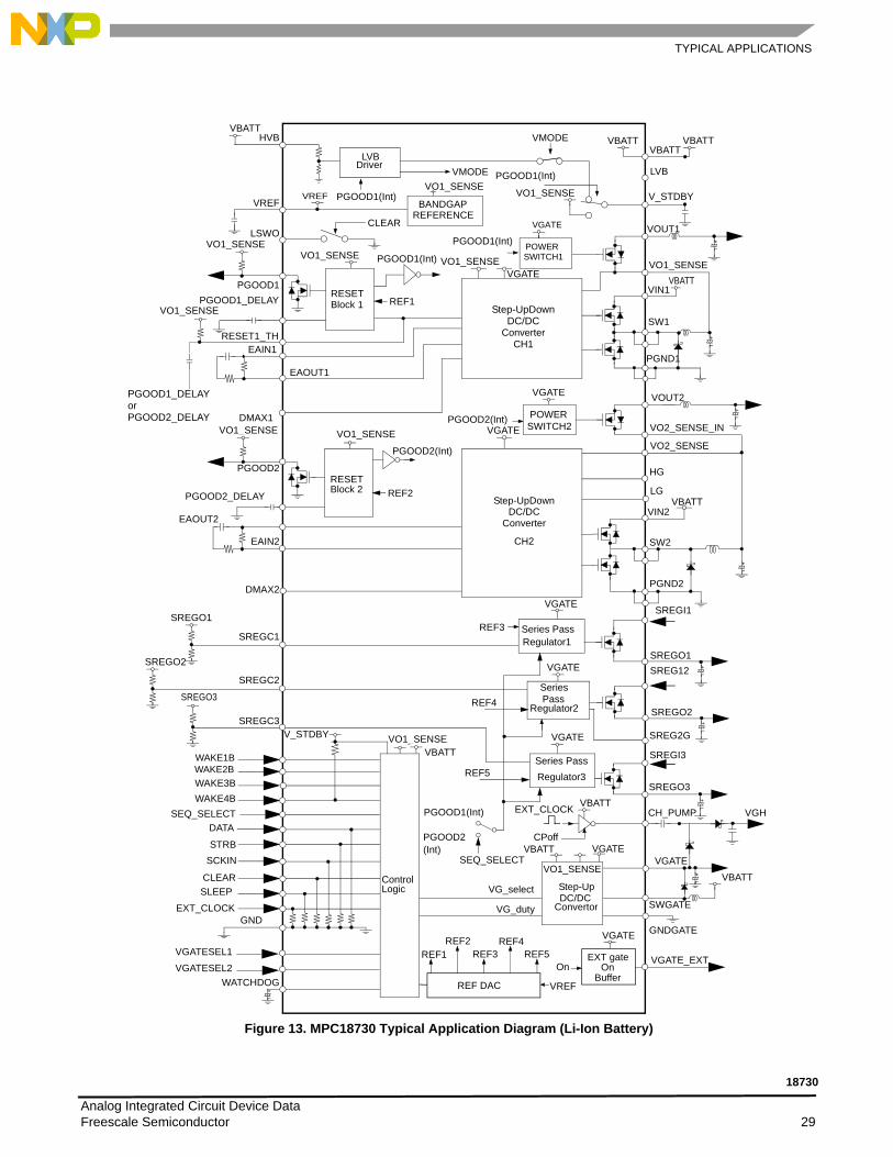
Figure 13. MPC18730 Typical Application Diagram (Li-Ion Battery)
VGATE_EXT
VREF
DMAX1
VO1_SENSE
PGND1
VOUT1
SW2
VBATTVBATT
LVB
HVB
EAOUT2
EAIN2
DMAX2
VO1_SENSE
PGOOD2_DELAY
PGND2
VIN2
VO2_SENSE
VOUT2
VBATT
VO2_SENSE_IN
DATA
VGATE
SREGO1
SREGC1
SREGC2
SREGC3
GNDGATE
SREGI1
WATCHDOG
GND
SEQ_SELECT CH_PUMP
SREGO2
SREGO3
SREGI3
CLEAR
BANDGAP
VO1_SENSE
VBATT
VGATE
POWERSWITCH1
LVB
PGOOD1(Int)
PGOOD1(Int)
PGOOD1(Int)
Driver
REFERENCE
VO1_SENSE
Step-UpDownDC/DC
VMODE
PGOOD1(Int)
VREF
VGATE
POWERSWITCH2
REF2
PGOOD2(Int)VGATE
Step-UpDownDC/DC
PGOOD2(Int)
CONTROL
V_STDBY VO1_SENSE
Series Pass
VGATE
VGATEVBATT
VREF
Regulator1
Series
VGATE
VBATT
REF3
REF4
REF5
EXT_CLOCK
REF1REF2
REF3 REF4
REF5
REF DAC
Series Pass
VGATE
Regulator3
Regulator2
CPoff
VG_duty
VG_select
VGATESEL1VGATESEL2
VGATE
VO1_SENSE
HG
LG
PGOOD1_DELAYorPGOOD2_DELAY
SW1
SWGATE
OnEXT gate
On
EXT_CLOCK
CLEAR
SCKIN
WAKE2BWAKE3BWAKE4B
SREGO3
PGOOD2
RESET1_TH
PGOOD1
LSWO
SLEEP
PGOOD1_DELAY
Buffer
SREGO1
SREGO2
SREG2G
ControlLogic Step-Up
DC/DCConvertor
Converter
RESETBlock 2
VO1_SENSE
RESET
PGOOD2
CH1
Converter
CH2
VBATT
VGH
Pass
(Int)
VGATE
VO1_SENSE
VBATT
SEQ_SELECT
PGOOD1(Int)
EAIN1
EAOUT1
VIN1
VO1_SENSE
V_STDBYVO1_SENSEVO1_SENSE
VMODE
STRB
VBATT
SREG12
WAKE1B
Block 1
VBATT
REF1
Analog Integrated Circuit Device Data Freescale Semiconductor 29
18730

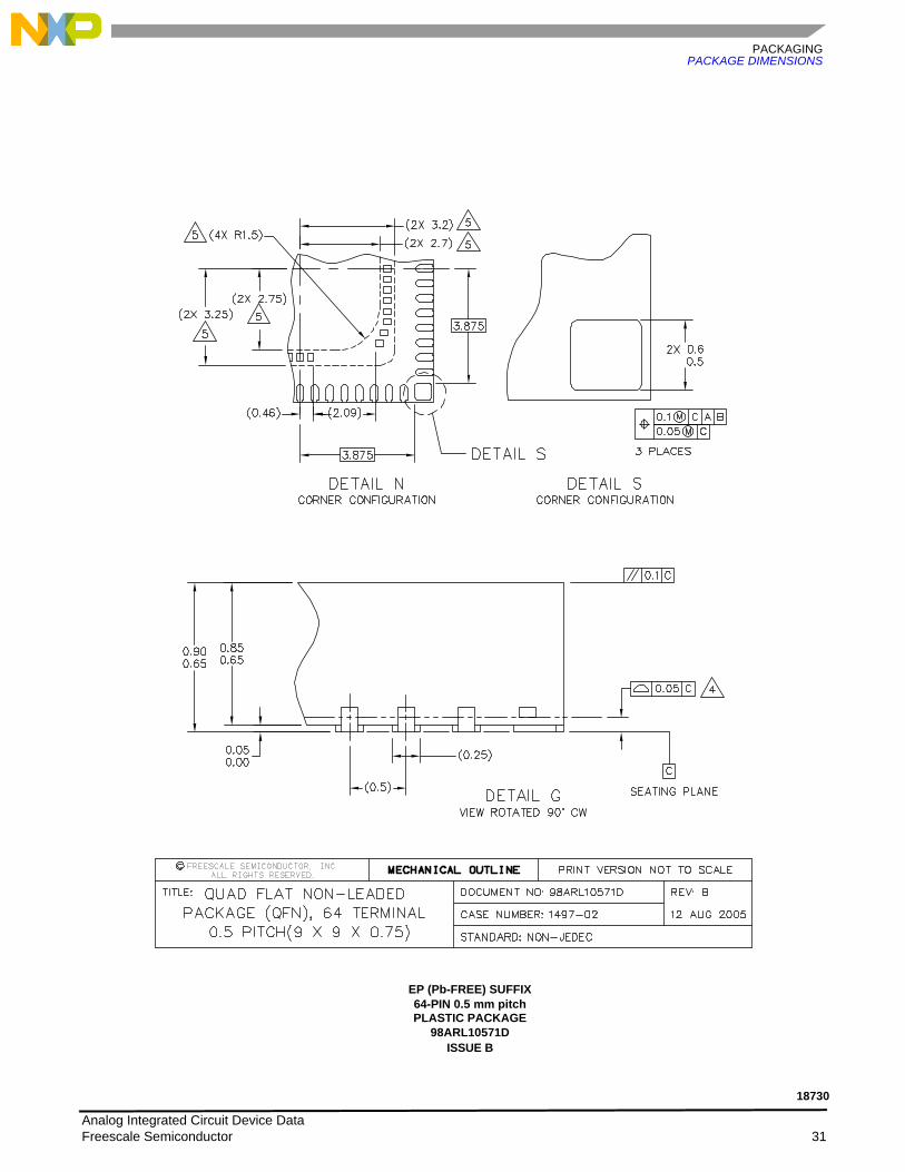
PACKAGINGPACKAGE DIMENSIONS
PACKAGING
PACKAGE DIMENSIONS
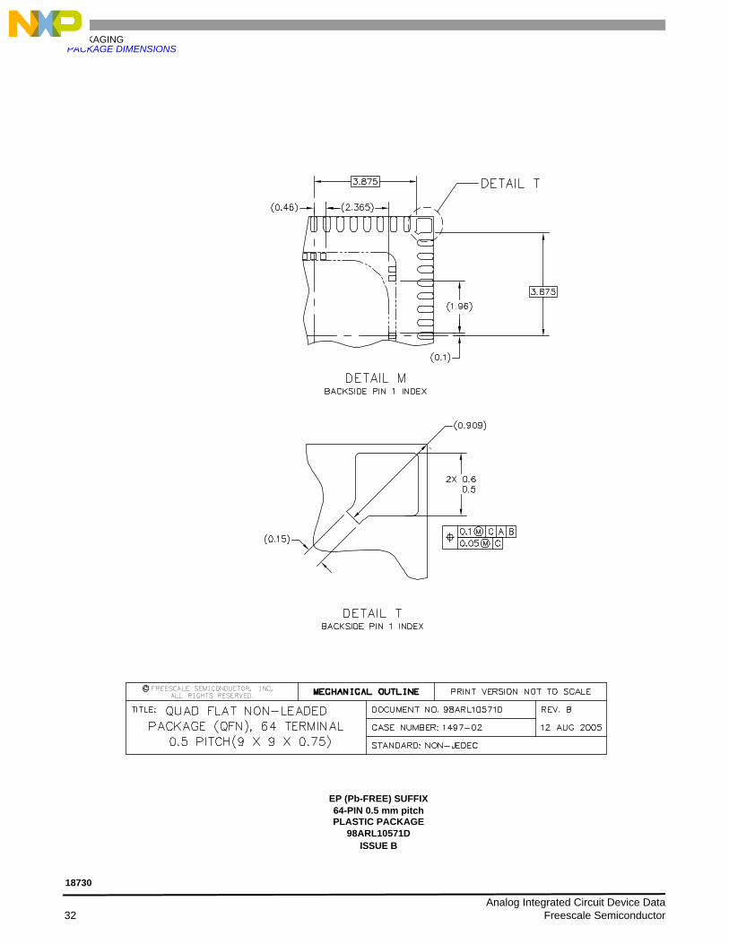
For the most current package revision, visit www.freescale.com and perform a keyword search using the “98A” listed below.
EP (Pb-FREE) SUFFIX64-PIN 0.5 mm pitchPLASTIC PACKAGE
98ARL10571DISSUE B
Analog Integrated Circuit Device Data 30 Freescale Semiconductor
18730
PACKAGINGPACKAGE DIMENSIONS
EP (Pb-FREE) SUFFIX64-PIN 0.5 mm pitchPLASTIC PACKAGE
98ARL10571DISSUE B
Analog Integrated Circuit Device Data Freescale Semiconductor 31
18730
PACKAGINGPACKAGE DIMENSIONS
EP (Pb-FREE) SUFFIX64-PIN 0.5 mm pitchPLASTIC PACKAGE
98ARL10571DISSUE B
Analog Integrated Circuit Device Data 32 Freescale Semiconductor
18730

PACKAGINGPACKAGE DIMENSIONS
EP (Pb-FREE) SUFFIX64-PIN 0.5 mm pitchPLASTIC PACKAGE
98ARL10571DISSUE B
Analog Integrated Circuit Device Data Freescale Semiconductor 33
18730

REVISION HISTORY
REVISION HISTORY
REVISION DATE DESCRIPTION OF CHANGES
3.0 04/2006 • Changed 34 of 64 Pin names to align with Application Note, AN3247 Rev 1.0.
4.0 8/2006 • Minor changes to correct errors and inconsistencies.• Updated form and style.
Analog Integrated Circuit Device Data 34 Freescale Semiconductor
18730

MPC18730Rev. 4.08/2006
Information in this document is provided solely to enable system and software implementers to use Freescale Semiconductor products. There are no express or implied copyright licenses granted hereunder to design or fabricate any integrated circuits or integrated circuits based on the information in this document.
Freescale Semiconductor reserves the right to make changes without further notice to any products herein. Freescale Semiconductor makes no warranty, representation or guarantee regarding the suitability of its products for any particular purpose, nor does Freescale Semiconductor assume any liability arising out of the application or use of any product or circuit, and specifically disclaims any and all liability, including without limitation consequential or incidental damages. “Typical” parameters that may be provided in Freescale Semiconductor data sheets and/or specifications can and do vary in different applications and actual performance may vary over time. All operating parameters, including “Typicals”, must be validated for each customer application by customer’s technical experts. Freescale Semiconductor does not convey any license under its patent rights nor the rights of others. Freescale Semiconductor products are not designed, intended, or authorized for use as components in systems intended for surgical implant into the body, or other applications intended to support or sustain life, or for any other application in which the failure of the Freescale Semiconductor product could create a situation where personal injury or death may occur. Should Buyer purchase or use Freescale Semiconductor products for any such unintended or unauthorized application, Buyer shall indemnify and hold Freescale Semiconductor and its officers, employees, subsidiaries, affiliates, and distributors harmless against all claims, costs, damages, and expenses, and reasonable attorney fees arising out of, directly or indirectly, any claim of personal injury or death associated with such unintended or unauthorized use, even if such claim alleges that Freescale Semiconductor was negligent regarding the design or manufacture of the part.
Freescale™ and the Freescale logo are trademarks of Freescale Semiconductor, Inc. All other product or service names are the property of their respective owners.© Freescale Semiconductor, Inc., 2006. All rights reserved.
How to Reach Us:
Home Page:www.freescale.com
E-mail:[email protected]
USA/Europe or Locations Not Listed:Freescale SemiconductorTechnical Information Center, CH3701300 N. Alma School Road Chandler, Arizona 85224 +1-800-521-6274 or [email protected]
Europe, Middle East, and Africa:Freescale Halbleiter Deutschland GmbHTechnical Information CenterSchatzbogen 781829 Muenchen, Germany+44 1296 380 456 (English)+46 8 52200080 (English)+49 89 92103 559 (German)+33 1 69 35 48 48 (French)[email protected]
Japan:Freescale Semiconductor Japan Ltd. Headquarters ARCO Tower 15F 1-8-1, Shimo-Meguro, Meguro-ku, Tokyo 153-0064 Japan 0120 191014 or +81 3 5437 [email protected]
Asia/Pacific:Freescale Semiconductor Hong Kong Ltd.Technical Information Center 2 Dai King Street Tai Po Industrial Estate Tai Po, N.T., Hong Kong +800 2666 [email protected]
For Literature Requests Only:Freescale Semiconductor Literature Distribution CenterP.O. Box 5405Denver, Colorado 802171-800-441-2447 or 303-675-2140Fax: [email protected]