mpc5500 flash programming through nexus/ · pdf fileon-chip emulation (once) mpc5500 flash...
TRANSCRIPT

Freescale SemiconductorApplication Note
AN3283Rev. 0.1, 06/2006
Table of Contents1 JTAG....................................................................22 On-Chip Emulation (OnCE).................................53 Nexus Read/Write Access Block .......................214 System Initialization...........................................265 Creating the Flash Programming Tool ...............286 Revision History ................................................33
MPC5500 Flash Programming Through Nexus/JTAGby: Kyle Norman
MCD Applications
The MPC5500 family of devices has internal Flash used for code and data.1 The Nexus debug interface can be used to program the Flash using the JTAG communication protocol through the JTAG port. This allows programming of the internal Flash by an external tool.
This application note first addresses the JTAG and Nexus communication protocol. The JTAG discussion includes the JTAG signals, TAP controller state machine, and the JTAG controller. The explanation of Nexus includes the on-chip emulation (OnCE) module and the Nexus read/write (R/W) access block.
After the communication protocols are described, this document goes into details of the Freescale-provided Flash drivers and the requirements of the external tool for Flash programming. For the purpose of this document, the external tool consists of a PC application combined with interface hardware that connects the PC to the JTAG port on an MPC5500 board or module.
1. The internal Flash on the MPC5500 devices can also be used for EEPROM emulation. See the white paper titled “MPC5500 Using Flash as EEPROM” for details.
© Freescale Semiconductor, Inc., 2006. All rights reserved.

JTAG
This document is intended for anyone wanting to develop a Flash programming tool for the MPC5500 family of devices. Someone wanting to learn about the JTAG communication protocol, OnCE module, or the Nexus R/W access block may also find this application note beneficial.
1 JTAGJTAG is a serial communication protocol developed by the Joint Test Access Group. Originally developed for boundary scan, JTAG is also used for communication with the Nexus debug interface (NDI) on the MPC5500 devices. Figure 2 shows a block diagram of the NDI.
1.1 JTAG SignalsThe JTAG port of the MPC5500 devices consists of the TCK, TDI, TDO, TMS, and JCOMP pins. TDI, TDO, TMS, and TCK are compliant with the IEEE 1149.1-2001 standard and are shared with the NDI through the test access port (TAP) interface. See Table 1 for signal properties.
1.2 TAP Controller State MachineThe TAP controller state machine controls the JTAG logic. The TAP controller state machine is a 16-state finite state machine (FSM) as shown in Figure 1. The TCK and TMS signals control transition between states of the FSM. These two signals control whether an instruction register scan or data register scan is performed. Both the TDI and TMS inputs are sampled on the rising edge of TCK while the TDO output changes on the falling edge of TCK. The value shown next to each state of the state machine in Figure 1 is the value of TMS required on the rising edge of TCK to transition to the connected state. Five rising edges of TCK with TMS at logic 1 guarantees entry into the TEST LOGIC RESET state.
Table 1. JTAG Signal Properties
Name I/O Function
TCK I Test Clock
TDI I Test Data In
TDO O Test Data Out
TMS I Test Mode Select
JCOMP I JTAG Compliancy
MPC5500 Flash Programming Through Nexus/JTAG, Rev. 0.1
Freescale Semiconductor2

JTAG
Figure 1. TAP Controller Finite State Machine
TEST LOGICRESET
RUN-TEST/IDLE SELECT-DR-SCAN SELECT-IR-SCAN
CAPTURE-DR CAPTURE-IR
SHIFT-DR SHIFT-IR
EXIT1-DR EXIT1-IR
PAUSE-DR PAUSE-IR
EXIT2-DR EXIT2-IR
UPDATE-DR UPDATE-IR
1
0
111
0 0
0 0
1 1
0 0
1 1
1 1
0 0
0 0
1 1
1 1
0 0
1 10 0
0
NOTE: The value shown adjacent to each state transition in this figure represents the value of TMS at the time of a rising edge of TCK.
MPC5500 Flash Programming Through Nexus/JTAG, Rev. 0.1
Freescale Semiconductor 3

JTAG
1.3 JTAG Controller (JTAGC)The MPC5500 family of devices have a JTAG controller (JTAGC) that enables both boundary scan and communication with the Nexus development interface (NDI). A block diagram of the NDI is shown in Figure 2.
Figure 2. Nexus Development Interface (NDI) Block Diagram
1.3.1 JTAGC ResetThe JTAGC is placed in reset when the TAP controller state machine is in the test logic reset state. The test logic reset state is entered upon the assertion of the power-on reset signal, negation of JCOMP, or through TAP controller state machine transitions controlled by TMS. Asserting power-on reset or negat-ing JCOMP results in asynchronous entry into the test logic reset state.
JCOMP
Program, Data,Ownership,Watchpoint,
Trace
R/W Register,Halt, Step,Continue
Data,Watchpoint,
Trace
Buffer
Program, Data,Ownership,Watchpoint,
Trace
R/W Register,R/W Data,Halt, Step,Continue
Read/WriteAccess
Cache
NZ6C3
Nexus Port Controller(NPC)
JTAG Port Controller (JTAGC)
RDY TDI TCK TDO TMS EVTI
Auxiliary Port
MSEO[0:1] MCKO MDO(4 or 12) EVTO• • •
Buffer
Off-ChipMemory & I/O
XBAR
eDMAC
MMU
e200z6
Engine1
CDC
Engine2*
eTPU
NXDM
Data,Watchpoint,
Trace
Buffer
NXFR
FlexRay
On-ChipMemory & I/O
Buffer
* Some MPC55xx devices have one eTPU engine, others have two engines.
NDEDI
MPC5500 Flash Programming Through Nexus/JTAG, Rev. 0.1
Freescale Semiconductor4

On-Chip Emulation (OnCE)
1.3.2 TAP SharingThe JTAGC allows communication with the NDI by sharing the test access port (TAP) with other TAP controllers. The JTAGC initially has control of the TAP after the assertion of power-on reset or the negation of JCOMP. As an example, selectable NDI TAP controllers for the MPC5554 include the Nexus port controller, e200z6 OnCE, eTPU Nexus, and eDMA Nexus. The NDI TAP controllers are selected by loading the appropriate opcode into the 5-bit instruction register of the JTAGC while JCOMP is asserted. Table 2 shows the opcodes for the selectable TAP controllers. When one of these opcodes is loaded, control of the TAP pins is transferred to the selected auxiliary TAP controller. Any data input via TDI and TMS is passed to the selected TAP controller, and any TDO output from the selected TAP controller is sent back to the JTAGC to be output on the TDO pin.
The JTAGC regains control of the TAP during the UPDATE-DR state if the PAUSE-DR state was entered. Auxiliary TAP controllers are held in RUN-TEST/IDLE while they are inactive. This document will focus on the OnCE TAP controller. While access to the other TAP controllers is similar, they are outside the scope of this document and are not needed for Flash programming.
2 On-Chip Emulation (OnCE)All of the MPC5500 devices possess a OnCE module for debug control of the PowerPC e200 core. The OnCE logic provides Nexus class 1 static debug capability including run-time control, register access, and memory access to all memory-mapped regions including on-chip peripherals. The OnCE module is controlled by the JTAG signals through the OnCE TAP controller.
2.1 Enabling the OnCE TAP ControllerControl of the OnCE module is obtained through the OnCE TAP controller. To enable the OnCE TAP controller, the JTAGC must have control of the TAP and the ACCESS_AUX_TAP_ONCE (0b10001) opcode must be loaded into the 5-bit JTAGC instruction register with the JCOMP signal set to a logic 1. The JTAGC instruction register is loaded by scanning in the appropriate bits on the TDI pin, least significant bit (LSB) first, while in the SHIFT-IR state of the TAP controller state machine shown in Figure 1. The last bit is shifted in with TMS set to a logical 1 causing transition from the SHIFT-IR state to the EXIT1-IR state. Table 3 shows the steps required to enable the OnCE TAP controller, assuming the TAP controller state machine is initially in the RUN-TEST/IDLE state. The state machine is returned to the RUN-TEST/IDLE state when the write is complete.
Table 2. JTAG Client Select Instructions
JTAGC Instruction Opcode Description
ACCESS_AUX_TAP_NPC 10000 Enables access to the NPC TAP controller
ACCESS_AUX_TAP_ONCE 10001 Enables access to the e200z6 OnCE TAP controller
ACCESS_AUX_TAP_eTPU 10010 Enables access to the eTPU Nexus TAP controller
ACCESS_AUX_TAP_DMA 10011 Enables access to the eDMA Nexus TAP controller
ACCESS_AUX_TAP_NXFR 10100 Enables access to the FlexRay Nexus TAP controller
MPC5500 Flash Programming Through Nexus/JTAG, Rev. 0.1
Freescale Semiconductor 5

On-Chip Emulation (OnCE)
Figure 3 shows the required signal transitions on a logic analyzer for enabling the OnCE TAP controller.
Figure 3. Signal Transitions for Enabling the OnCE TAP Controller
2.2 OnCE Register AccessThe OnCE module provides several registers for static debug support. The OnCE command register (OCMD) is a special register and acts as the IR for the TAP controller state machine and is used to access other OnCE resources.
2.2.1 OnCE Command RegisterThe OnCE command register (OCMD) is a 10-bit shift register that receives its serial data from the TDI pin and acts as the IR register of the TAP controller state machine. The OCMD is updated when the TAP
Table 3. Steps for Enabling the OnCE TAP Controller
TCK Tick TMS TDI Resulting State
1 1 X1
NOTES:1 A value of X signifies that the signal value does not
matter.
SELECT-DR-SCAN
2 1 X SELECT-IR-SCAN
3 0 X CAPTURE-IR
4 0 X SHIFT-IR
5 0 1 SHIFT-IR
6 0 0 SHIFT-IR
7 0 0 SHIFT-IR
8 0 0 SHIFT-IR
9 1 1 EXIT1-IR
10 1 X UPDATE-IR
11 0 X RUN-TEST/IDLE
Data starts onthis clock edge
1 0 0 0 1
MPC5500 Flash Programming Through Nexus/JTAG, Rev. 0.1
Freescale Semiconductor6

On-Chip Emulation (OnCE)
controller enters the UPDATE-IR state. It contains fields for controlling access to a resource, as well as controlling single step operations and exit from debug mode. Figure 4 shows the register definition for the OnCE command register.
Figure 4. OnCE Command Register
Table 4 provides bit definitions for the once command register.
R/W GO EX RS[0:6]
0 1 2 3 4 5 6 7 8 9
Reset - 0b10_0000_0010 on assertion of JCOMP, during power on reset, or while in the TEST LOGIC RESET state
Table 4. OnCE Command Register Bit Definitions
Bit(s) Name Description
0 R/W Read/Write Command Bit The R/W bit specifies the direction of data transfer. The table below describes the options defined by the R/W bit.0 Write the data associated with the command into the register specified by RS[0:6]1 Read the data contained in the register specified by RS[0:6]Note: The R/W bit is ignored for read-only or write-only registers. In addition, it is ignored for all bypass operations. When performing writes, most registers are sampled in the Capture-DR state into a 32-bit shift register, and subsequently shifted out on TDO during the first 32 clocks of Shift-DR.
1 GO Go Command Bit 0 Inactive (no action taken) 1 Execute instruction in IR If the GO bit is set, the chip will execute the instruction which resides in the IR register in the CPUSCR. To execute the instruction, the processor leaves debug mode, executes the instruction, and if the EX bit is cleared, returns to debug mode immediately after executing the instruction. The processor goes on to normal operation if the EX bit is set, and no other debug request source is asserted. The GO command is executed only if the operation is a read/write to CPUSCR or a read/write to “No Register Selected”. Otherwise the GO bit is ignored.The processor will leave debug mode after the TAP controller Update-DR state is entered.On a GO+NoExit operation, returning to debug mode is treated as a debug event, thus exceptions such as machine checks and interrupts may take priority and prevent execution of the intended instruction. Debug firmware should mask these exceptions as appropriate. The OSR[ERR] bit indicates such an occurrence.
MPC5500 Flash Programming Through Nexus/JTAG, Rev. 0.1
Freescale Semiconductor 7

On-Chip Emulation (OnCE)
Table 5 shows the OnCE register addresses. Access to the registers CPUSCR, DAC1-2, DBCNT, DBCR0-3, DBSR, and IAC1-4 require that the external debug mode bit, DBCR0[EDM], be set to a logical 1. Only the DBCR0[EDM] is accessible in the DBCR0 register prior to that bit being set. Setting DBCR0[EDM] enables external debug mode and disables software updates to debug registers. The CPU should be placed in debug mode via the OCR[DR] bit prior to setting the DBCR0[EDM] bit. For more information on enabling external debug mode, see Section 2.5, “Enabling External Debug Mode and Other Initialization.”
2 EX Exit Command Bit 0 Remain in debug mode 1 Leave debug mode If the EX bit is set, the processor will leave debug mode and resume normal operation until another debug request is generated. The Exit command is executed only if the Go command is issued, and the operation is a read/write to CPUSCR or a read/write to “No Register Selected”. Otherwise the EX bit is ignored. The processor will leave debug mode after the TAP controller Update-DR state is entered. Note that if the DR bit in the OnCE control register is set or remains set, or if a bit in the DBSR is set, or if a bit in the DBSR is set and DBCR0[EDM]=1 (external debug mode is enabled), then the processor may return to debug mode without execution of an instruction, even though the EX bit was set.
3–9 RS Register SelectThe Register Select bits define which register is source (destination) for the read (write) operation. Attempted writes to read-only registers are ignored.
Table 5. OnCE Register Addressing
RS[0:6] Register Selected
000 0000 Reserved
000 0001 Reserved
000 0010 JTAG ID (read-only)
000 0011-000 1111
Reserved
001 0000 CPU Scan Register (CPUSCR)
001 0001 No Register Selected (Bypass)
001 0010 OnCE Control Register (OCR)
001 0011 Reserved
001 0100 -001 1111
Reserved
010 0000 Instruction Address Compare 1 (IAC1)
010 0001 Instruction Address Compare 2 (IAC2)
010 0010 Instruction Address Compare 3 (IAC3)
010 0011 Instruction Address Compare 4 (IAC4)
Table 4. OnCE Command Register Bit Definitions (continued)
Bit(s) Name Description
MPC5500 Flash Programming Through Nexus/JTAG, Rev. 0.1
Freescale Semiconductor8

On-Chip Emulation (OnCE)
2.2.2 Example of OnCE Register WriteOnCE registers can be written by selecting the register using the RS[0:6] field and clearing the R/W bit in the OnCE command register (OCMD). This requires a scan through the IR path of the TAP controller state machine to write the OCMD and a scan through the DR path of the TAP controller state machine to write the selected register. As mentioned above, the external debug mode bit, DBCR0[EDM], must be set to a logical 1 to allow access to most of the OnCE registers. Therefore, writing the DCBR0 register to set the EDM bit is used as an example of a writing a OnCE register. Figure 5 shows the register definition of DBCR0.
010 0100 Data Address Compare 1 (DAC1)
010 0101 Data Address Compare 2 (DAC2)
010 0110 -010 1011
Reserved
010 1100 Debug Counter Register (DBCNT)
010 1101 Debug PCFIFO (PCFIFO) (read-only)
010 1110 -010 1111
Reserved
011 0000 Debug Status Register (DBSR)
011 0001 Debug Control Register 0 (DBCR0)
011 0010 Debug Control Register 1 (DBCR1)
011 0011 Debug Control Register 2 (DBCR2)
011 0100 Debug Control Register 3 (DBCR3)
011 0101-101 1111
Reserved
111 0000 -111 1001
General Purpose register selects [0:9]
111 1010 Cache Debug Access Control Register (CDACNTL)
111 1011 Cache Debug Access Data Register (CDADATA)
111 1100 Nexus3-Access
111 1101 Reserved
111 1110 Enable_OnCE1
111 1111 Bypass
NOTES:1 It is not necessary to enable the OnCE module on the MPC5500 devices.
Table 5. OnCE Register Addressing (continued)
RS[0:6] Register Selected
MPC5500 Flash Programming Through Nexus/JTAG, Rev. 0.1
Freescale Semiconductor 9

On-Chip Emulation (OnCE)
Figure 5. DBCR0 Register
The example of writing DBCR0 is divided into two parts: writing OCMD to select a write to DBCR0, and writing the value 0x80000000 to DBCR0. All data will be scanned in least significant bit first.
Figure 6 shows writing the value 0b00_0011_0001 to OCMD through the IR path to select a write to DBCR0 assuming the TAP controller state machine is initially in the RUN-TEST/IDLE state. The state machine is returned to the RUN-TEST/IDLE state when the write is complete.
Figure 6. Signal Transitions for Writing OCMD to Select a Write to DBCR0
Figure 7 shows writing the value 0x80000000 to DBCR0 through the DR path to set the EDM bit assuming the TAP controller state machine is initially in the RUN-TEST/IDLE state. The state machine is returned to the RUN-TEST/IDLE state when the write is complete.
0 1 2 3 4 5 6 7 8 9 10 11 12 13 14 15
R EDM IDM RST ICMP BRT IRPT TRAP IAC1 IAC2 IAC3 IAC4 DAC1 DAC2
W
Reset 01
NOTES:1 DBCR0[EDM] is affected by a Nexus port reset or a power on reset, but not by an assertion of RESET. All other bits
are reset by processor reset (including assertion of RESET) as well as by a power on reset.
0 0 0 0 0 0 0 0 0 0 0 0 0 0 0
16 17 18 19 20 21 22 23 24 25 26 27 28 29 30 31
R RET 0 0 0 0 DEVT1 DEVT2 DCNT1 DCNT2 CIRPT CRET 0 0 0 0 FT
W
Reset 0 0 0 0 0 0 0 0 0 0 0 0 0 0 0 0
Data starts onthis clock edge
1 0 0 0 1 1 0 0 0 0
MPC5500 Flash Programming Through Nexus/JTAG, Rev. 0.1
Freescale Semiconductor10

On-Chip Emulation (OnCE)
Figure 7. Signal Transitions for Writing DBCR0
2.2.3 Example of OnCE Register ReadOnCE registers can be read by selecting the register using the RS[0:6] field and setting the R/W bit in the OnCE command register (OCMD). This requires a scan through the IR path of the TAP controller state machine to write the OCMD and a scan through the DR path of the TAP controller state machine to read the selected register. A write to DBCR0 to set the EDM bit was used for an example of a writing a OnCE register, Section 2.2.2, “Example of OnCE Register Write,” so this read example will read DBCR0 after the EDM bit is set. Figure 5 shows the register definition of the DBCR0.
Figure 8 shows writing the value 0b10_0011_0001 to OCMD through the IR path to select a read from DBCR0 assuming the TAP controller state machine is initially in the RUN-TEST/IDLE state. The state machine is returned to the RUN-TEST/IDLE state when the write is complete.
Figure 8. Signal Transitions for Writing OCMD to Select a Read from DBCR0
Figure 9 shows reading the value 0x80000000 from DBCR0 through the DR path assuming the TAP controller state machine is initially in the RUN-TEST/IDLE state. The state machine is returned to the RUN-TEST/IDLE state when the read is complete.
Data starts on this clock edge
0 0 0 0 0 0 0 0 0 0 0 0 0 0 0 0 0 0 0 0 0 0 0 0 0 0 0 0 0 0 0 1
Data starts onthis clock edge
1 0 0 0 1 1 0 0 0 1
MPC5500 Flash Programming Through Nexus/JTAG, Rev. 0.1
Freescale Semiconductor 11

On-Chip Emulation (OnCE)
Figure 9. Signal Transitions for Reading DBCR0
2.3 OnCE Status RegisterThe OnCE status register (OSR) is a special register in terms of how it is read. Status information related to the state of the CPU is latched into the OnCE status register when the OnCE TAP controller state machine enters the CAPTURE-IR state. The status information is shifted out serially through the SHIFT-IR state on TDO. The OSR is a 10-bit register like the OCMD. Therefore, the status information can be read while writing OCMD. The OSR is shown in Figure 10.
Figure 11 shows reading the OnCE status register on TDO while writing the OCMD on TDI assuming the TAP controller state machine is initially in the RUN-TEST/IDLE state. The state machine is returned to the RUN-TEST/IDLE state when the read is complete. The OCMD is written with the value 0b10_0001_0001 choosing a read of No Register Selected. The data read on TDO from the OnCE status register is 0b10_0000_1001 showing that the OSR[MCLK] and OSR[DEBUG] status bits are set. All data is scanned in and out least significant bit first.
MCLK ERR CHKSTOP RESET HALT STOP DEBUG 0 1
0 1 2 3 4 5 6 7 8 9
Figure 10. OnCE Status Register
Data starts onthis clock edge
0 0 0 0 0 0 0 0 0 0 0 0 0 0 0 0 0 0 0 0 0 0 0 0 0 0 0 0 0 0 0 1
MPC5500 Flash Programming Through Nexus/JTAG, Rev. 0.1
Freescale Semiconductor12

On-Chip Emulation (OnCE)
Figure 11. Signal Transitions of Reading the OnCE Status Register
2.4 Entering Debug Mode During ResetThere are several different methods of entering debug mode. This section will cover entering debug mode while the RESET pin is asserted. Entering debug mode while the RESET pin is asserted is useful, because the debug session will begin with the CPU in a known state. The OnCE control register (OCR) controls entry into debug mode for this method. Figure 12 shows the register definition for the OCR.
The OCR[DR] bit is the CPU debug request control bit and requests the CPU to unconditionally enter debug mode. The OCR[WKUP] bit is the wakeup request bit used to guarantee that the CPU clock is running. Debug status and CPU clock activity can be determined by reading the DEBUG and MCLK bits in the OnCE status register. After entering debug mode, the OCR[DR] bit should be cleared leaving the OCR[WKUP] bit set. OCR[FDB] should also then be set to enable recognition of software breakpoints. See Section 2.12.1, “Software Breakpoints” for details on software breakpoints. The steps required for entering debug mode during reset assuming the OnCE TAP controller has been enabled via the method described in Section 2.1, “Enabling the OnCE TAP Controller” are listed below:
1. Assert RESET.2. Set the OCR[DR] and OCR[WKUP] bits.3. De-assert RESET.4. Verify debug mode via the DEBUG bit in the OnCE status register.5. Clear the OCR[DR] bit while leaving OCR[WKUP] set and set OCR[FDB].
For programming the Flash through the Nexus port, the boot configuration pins must be set to a value that enables both Nexus and the internal Flash prior to the assertion of RESET. Table 6 shows the boot configuration options.
0 DMDIS 0 DW DI DM DG DE 0 WKUP FDB DR
0 1 2 3 4 5 6 7 8 9 10 11 12 13 14 15 16 17 18 19 20 21 22 23 24 25 26 27 28 29 30 31
Reset - 0x0000_0000 on negation of JCOMP, power on reset, or entering TEST LOGIC RESET state
Figure 12. OnCE Control Register
Data starts onthis clock edgeData starts on
this clock edge
1 0 0 0 1 0 0 0 0 1
1 0 0 1 0 0 0 0 0 1
MPC5500 Flash Programming Through Nexus/JTAG, Rev. 0.1
Freescale Semiconductor 13

On-Chip Emulation (OnCE)
2.5 Enabling External Debug Mode and Other InitializationBefore enabling external debug mode, the CPU should be placed into debug mode via the method outlined in Section 2.4, “Entering Debug Mode During Reset.” The external tool should then write the DBCR0[EDM] bit to enable external debug mode. Note that the first write to DBCR0 will only affect the EDM bit. All other bits in that register require DBCR0[EDM] to be set prior to writing them. After enabling external debug mode, the DBSR status bits should be cleared by writing 0xFFFFFFFF to DBSR using the method described in Section 2.2, “OnCE Register Access.” The register definition of DBSR is shown in Figure 13.
Figure 13. Debug Status Register (DBSR)
2.6 CPU Status and Control Scan Chain Register (CPUSCR)
CPU information is accessible via the OnCE module through a single scan chain register named the CPUSCR. The CPUSCR provides access to this CPU information and a mechanism for an external tool to set the CPU to a desired state before exiting debug mode. The CPUSCR also provides the ability to access
Table 6. Boot Modes
BOOTCFG[0:1]Censorship
Control0x00FF_FFE0
Serial Boot Control
0x00FF_FFE2Boot Mode Name
Internal Flash State
Nexus State
Serial Password
00 !0x55AA Don't care Internal - Censored Enabled Disabled Flash
0x55AA Internal - Public Enabled Enabled Public
01 Don't care 0x55AA Serial - Flash Password Enabled Disabled Flash
!0x55AA Serial - Public Password Disabled Enabled Public
10 !0x55AA Don't care External – No Arbitration - Censored
Disabled Enabled Public
0x55AA External – No Arbitration - Public Enabled Enabled Public
11 !0x55AA Don't care External – External Arbitration - Censored
Disabled Enabled Public
0x55AA External – External Arbitration - Public Enabled Enabled Public
’!’ = ’NOT’, meaning any value other than the value specified. Values 0x0000 and 0xFFFF should not be used.
0 1 2 3 4 5 6 7 8 9 10 11 12 13 14 15
R IDE UDE MRR ICMP BRT IRPT TRAP IAC1 IAC2 IAC3 IAC4 DAC1R
DAC1W
DAC2R
DAC2W
W
Reset 0 0 0 1 0 0 0 0 0 0 0 0 0 0 0 0
16 17 18 19 20 21 22 23 24 25 26 27 28 29 30 31
R RET 0 0 0 0 DEVT1
DEVT2
DCNT1
DCNT2
CIRPT
CRET 0 0 0 0 CNT1RG
W
Reset 0 0 0 0 0 0 0 0 0 0 0 0 0 0 0 0
MPC5500 Flash Programming Through Nexus/JTAG, Rev. 0.1
Freescale Semiconductor14

On-Chip Emulation (OnCE)
register and memory contents. Figure 14 shows the CPUSCR. Once debug mode has been entered, it is required to scan in and update the CPUSCR prior to exiting debug mode or single stepping. Access to the CPUSCR is controlled by the OCMD as described in Section 2.2, “OnCE Register Access.”
Figure 14. CPU Status and Control Scan Chain Register
2.6.1 Instruction Register (IR)After entering debug mode, the opcode of the next instruction to be executed will be in the instruction register (IR). The value in the IR should be saved for later restoration if continuation of the normal instruction stream is desired.
The external tool has the capability to put instructions directly into the instruction register (IR) via the CPUSCR. These instructions can then be executed by the debug control block. By selecting appropriate instructions and single stepping them, the external tool can examine or change memory locations or CPU registers. See Section 2.7, “Single Step” for details on single step.
TDO
TDI
TCK
MSR
WBBRhigh
32
320 31
0 31
PC32
0 31
IR32
0 31
CTL32
0 31
WBBRlow
320 31
MPC5500 Flash Programming Through Nexus/JTAG, Rev. 0.1
Freescale Semiconductor 15

On-Chip Emulation (OnCE)
2.6.2 Control State Register (CTL)The control state register (CTL) stores the value of certain internal CPU state variables before debug mode is entered. Figure 15 shows the CTL register.
The “*” in the CTL register represents internal processor state bits that should be restored to the value they held when debug mode was entered prior to exiting debug mode. If a single step is executing an instruction that is in the normal instruction flow of the program that was running when debug mode was entered, these bits should be restored. If a single step is executing an instruction outside the normal instruction flow, these bits should be cleared to zero.
The PCOFST field indicates whether the value in the PC portion of the CPUSCR must be adjusted prior to exiting debug mode. Due to the pipelined nature of the CPU, the PC value must be backed-up under certain circumstances. The PCOFST field specifies the value to be subtracted from the PC value when debug mode was entered. This PC value should be adjusted according to PCOFST prior to exit from debug mode if continuation of the normal instruction stream is desired. In the event that PCOFST is non-zero, the IR should be loaded with a nop instruction instead of the value in the IR when debug mode was entered. Below are the possible values and meanings of the PCOFST field.
0000—No correction required.0001—Subtract 0x04 from PC.0010—Subtract 0x08 from PC.0011—Subtract 0x0C from PC.0100—Subtract 0x10 from PC.0101—Subtract 0x14 from PC.All other encodings are reserved.
After entering debug mode, the PCINV field overrides the PCOFST field and indicates that values in the PC and IR are invalid. Exiting debug mode with these PC and IR values will have unpredictable results.
No error condition exists.Error condition exists. PC and IR are corrupt.
The FFRA control bit causes the contents of WBBR to be used as the rA (rS for logical and shift operations) operand value of the first instruction to be executed when exiting debug mode or the instruction to be single stepped. This allows the external tool to update CPU registers and memory. rA and rS are instruction syntax used to identify a source GPR.
No action.Contents of WBBR used as rA (rS for logical and shift operations) operand value.
The IRStat0-9 bits provide status information to the external tool. The IRStat8 bit indicates that the instruction in the IR is a VLE or non-VLE instruction. For MPC5500 devices without VLE, bits IRstat8
*
PC
OF
ST
PC
INV
FF
RA
IRS
TAT
0
IRS
TAT
1
IRS
TAT
2
IRS
TAT
3
IRS
TAT
4
IRS
TAT
5
IRS
TAT
6
IRS
TAT
7
IRS
TAT
8
IRS
TAT
9
0 1 2 3 4 5 6 7 8 9 10 11 12 13 14 15 16 17 18 19 20 21 22 23 24 25 26 27 28 29 30 31
Figure 15. Control State Register (CTL)
MPC5500 Flash Programming Through Nexus/JTAG, Rev. 0.1
Freescale Semiconductor16

On-Chip Emulation (OnCE)
and IRstat9 of the CTL do not exist. Below is a description of the IRStat8 bit. All other CTL bits will be discussed as needed.
IR contains a BookE instruction.IR contains a PowerPC VLE instruction, aligned in the most significant portion of IR if 16-bit.
2.6.3 Program Counter Register (PC)The PC stores the value of the program counter that was present when debug mode was entered. The PC value is affected by operations performed during debug mode and must be restored prior to exiting debug mode. It may be necessary to adjust the PC before exiting debug mode according the PCOFST field in the CTL. If the external tool desires to redirect program flow to an arbitrary location, the PC and IR should be initialized corresponding to the first instruction to be executed. Alternatively, the IR may be set to a nop instruction and the PC may be set to the location prior to the location at which it is desired to redirect flow. When debug mode is exited, the nop will execute and then instruction fetch and execution will begin at the location which it is desired to redirect flow.
2.6.4 Write-Back Bus Register (WBBRlow, WBBRhigh)WBBR is used as a means of passing operand information to/from the CPU from/to the external tool. Whenever the external tool needs to read the contents of a CPU register or memory location, it can force the CPU to single step an instruction that brings that information to WBBR. To write the contents of a CPU register or memory location, the external tool can force the CPU to single step an instruction that uses the information in WBBR. For the purpose of this document, only WBBRlow will be used. WBBRhigh is used for SPE instructions that generate 64-bit results or use 64-bit operands. Such instructions are outside the scope of this document.
2.6.5 Machine State Register (MSR)The MSR is used to read/write the machine state register of the CPU. This register is affected by operations performed while in debug mode. If consistency of the machine state is desired, the MSR should be saved when entering debug mode and restored prior to exiting debug mode.
2.7 Single StepSingle stepping of instructions is achieved by first placing the CPU in debug mode if the CPU is not already in debug mode. The next step is to write the appropriate information into the CPU scan chain register (CPUSCR), followed by writing to OCMD to set the OCMD[GO] bit and clear the OCMD[EX] bit with the OCMD[RS] field indicating either the CPUSCR or No Register Selected. The CPUSCR register is covered in Section 2.6, “CPU Status and Control Scan Chain Register (CPUSCR).” Once debug mode has been entered, it is required that a scan in and update to the CPUSCR must be performed prior to single stepping.
For single step, the CPU will return to debug mode after executing a single instruction. The external tool should read the OnCE status register (OSR) to verify that the CPU has returned to debug mode with no
MPC5500 Flash Programming Through Nexus/JTAG, Rev. 0.1
Freescale Semiconductor 17

On-Chip Emulation (OnCE)
error by verifying that the OSR[DEBUG] bit is set and OSR[ERR] bit is cleared. For details on reading the OSR, see Section 2.3, “OnCE Status Register.”
During single step, exception conditions can occur, if not masked, and may prevent the desired instruction from being executed. After stepping over the instruction, the core will fetch the next instruction. The new program counter and instruction will be loaded into the PC and IR portions of the CPUSCR. Care must be taken to insure that the next instruction fetch after the single step is to a valid memory location. See Section 4.1, “Setting Up the Memory Management Unit” and Section 4.2, “Internal SRAM Initialization” for details. For MPC5500 devices with VLE, the CTL[IRstat8] bit indicates that the instruction in the IR is a VLE or non-VLE instruction. The CTL[FFRA], CTL[IRStat8], and the CTL bits indicated by “*” should be set as appropriate before single stepping. All other CTL bits should be set to zero. See Section 2.6.2, “Control State Register (CTL)” for details on FFRA, IRStat8, and the bits indicated by “*”.
Single stepping can be used during normal execution of the instruction flow or to force execution of a particular instruction by loading the desired instruction into the IR portion of the CPUSCR. By forcing execution of particular instructions, single stepping can be used for memory and register access by the tool. See Section 2.11, “OnCE Memory Access”, Section 2.9, “GPR Access”, and Section 2.10, “SPR Access” for details.
2.8 Exit From Debug Mode to Normal ExecutionExiting debug mode and returning to normal execution is achieved by first clearing the OCR[DMDIS] and OCR[DR] bits if not already clear while leaving the OCR[MCLK] set. The next step is to write the appropriate information into the CPU scan chain register (CPUSCR), followed by a write to OCMD to set the OCMD[GO] bit and OCMD[EX] bit with the OCMD[RS] field indicating either the CPUSCR or No Register Selected. Once debug mode has been entered, it is required that a scan in and update to the CPUSCR be performed prior to exiting debug mode. The CPUSCR register is covered in Section 2.6, “CPU Status and Control Scan Chain Register (CPUSCR).” If continuation of the normal instruction stream is desired, the external tool is responsible for inspection of the CTL register value when debug mode was entered to determine if the PC is invalid or needs to be offset prior to exiting debug mode. Also, the internal state bits indicated by “*” in the CTL should be restored to their original value when debug mode was entered if continuation of the normal instruction stream is desired. The IRStatus bits of the CTL should be set to zero with the exception of CTL[IRStat8] on MPC5500 devices with VLE. CTL[IRStat8] indicates if the current instruction in the IR is a VLE or non-VLE instruction. See Section 2.6.2, “Control State Register (CTL)” for details.
To begin instruction execution from an arbitrary location, which is the case when executing the Freescale-provided Flash drivers, the PC should be set to the desired location for execution to begin minus 0x4. The IR should be set to a nop (ex: 0x60000000). Then exit debug mode as mentioned above. The nop will be executed, then the core will begin fetching instructions at the desired location for execution.
2.9 GPR AccessThe OnCE module provides the ability to read and write the general purpose registers (GPR) while in debug mode. Reading a general purpose register is achieved by single stepping over an ori instruction. As an example, to read the lower 32 bits of GPR r1, an ori r1,r1,0 instruction is executed, and the result of
MPC5500 Flash Programming Through Nexus/JTAG, Rev. 0.1
Freescale Semiconductor18

On-Chip Emulation (OnCE)
the instruction will be latched into WBBRlow. The external tool can then read the contents of WBBRlow by scanning out the CPUSCR.
Writing a register is achieved by single stepping over an ori instruction with the CTL[FFRA] bit set causing the WBBRlow to be used as the source register for the instruction. As an example, to write the lower 32 bit of GPR r1, an ori r1, X, 0 is executed with the data to be written in WBBRlow. The X in the instruction will be replaced by the WBBRlow register. See Section 2.7, “Single Step” for details on single stepping.
2.10 SPR AccessThe OnCE module provides the ability to read and write the special purpose registers (SPR) while in debug mode. Reading a special purpose register is achieved by saving the value in a GPR, single stepping over a mfspr instruction which brings the spr value into both the saved GPR and WBBRlow, and then restoring the GPR. As an example, to read SPR 624, first save r31. Then execute mfspr r31, 624. The value that was in SPR 624 will now be in WBBRlow of the CPUSCR and can be read by the external tool. Finally r31 should be restored.
To write an SPR, single step over a mtspr instruction with the value to write to the SPR in WBBRlow and the CTL[FFRA] bit set. For example, to write SPR 624 with the value 0x10050000, single step over mtspr 624, X with the value to write to SPR 624 in WBBRlow and CTL[FFRA] set. The X in the instruction will be replaced by WBBRlow. See Section 2.7, “Single Step” for details on single stepping.
DBCR0-3, DBSR, DBCNT, IAC1-4, DAC1-2 cannot be written by single stepping over mtspr like the other SPRs while in external debug mode. They can however be written by the method detailed in Section 2.2, “OnCE Register Access.”
2.11 OnCE Memory AccessThere are two ways to access memory mapped locations on the MPC5500 devices: one is through the OnCE module, and the other is through the Nexus R/W access block. The OnCE module method requires that the CPU be in debug mode and makes use of the memory management unit (MMU) and cache. The Nexus R/W access block does not require that the CPU be in debug mode and bypasses the MMU and cache. The Nexus R/W access block is also the faster method of accessing memory. This section will cover access to memory mapped locations using the OnCE method. The Nexus R/W access block will be covered in Section 3, “Nexus Read/Write Access Block.”
Writing a memory location is achieved by first reading the contents of a GPR and saving that value, writing that GPR with the value to be written to memory, and single stepping over a stw, sth, or stb instruction with the address to write in WBBRlow and the CTL[FFRA] bit set. The GPR that was previously saved should be used as the rS field of the store instruction. After single stepping over the store instruction, the saved GPR value should then be restored. For example, to write the word 0xA5A5A5A5 to location 0x40000000, first save the value in a r31. Then write the value 0xA5A5A5A5 to r31. The next step is to step over the instruction stw r31, 0(X) with 0x40000000 in WBBRlow and the CTL[FFRA] bit set. The X in the instruction is replaced by the WBBRlow register. GPR r31 should then be restored to its saved value.
Reading a memory location is achieved by first reading the contents of a GPR and saving that value, then single stepping a lwz, lhz, or lbz with the address to be read in WBBRlow and the CTL[FFRA] bit set. The
MPC5500 Flash Programming Through Nexus/JTAG, Rev. 0.1
Freescale Semiconductor19

On-Chip Emulation (OnCE)
GPR that was previously saved should be used as the rD field of the load instruction. The value read from the memory location will then be in both the WBBRlow and the GPR whose value was previously saved. After single stepping the load instruction and getting the read data from WBBRlow, the saved GPR value should then be restored. For example, to read a word from address location 0x40000000, first save the value in r31. Then single step over the instruction lwz r31, 0(X) with 0x40000000 in WBBRlow and the CTL[FFRA] bit set. The X in the instruction is replaced by the WBBRlow register. After the single step is complete, the data read from memory can be read by the external tool from WBBRlow. GPR r31 should then be restored to its saved value. See Section 2.7, “Single Step” for details on single stepping.
2.12 BreakpointsThe OnCE debug module provides the capability for both software and hardware breakpoints to be set at a particular address. For Flash programming using the Freescale provided Flash drivers, software breakpoints are the easiest to use. As a reference, instruction address hardware breakpoints will also be discussed in this section.
2.12.1 Software BreakpointsRecognition of software breakpoints by the OnCE module are enabled by setting the OCR[FDB] bit along with the DBCR0[EDM] bit. Upon executing a bkpt pseudo-instruction, the CPU enters debug mode after the instruction following the bkpt pseudo-instruction has entered the instruction register. The bkpt pseudo-instruction is defined to be an all 0’s instruction opcode. The Freescale-provided Flash drivers have the bkpt pseudo-instruction built in and execution of this instruction at the completion of the driver can be enabled or disabled. This feature of the drivers will be discussed in Section 5.2.2, “FlashInit.”
2.12.2 Instruction Address Hardware BreakpointsThe OnCE module provides the capability to set up to four instruction address hardware breakpoints. When an instruction address breakpoint is hit, the CPU will enter debug mode prior to executing the instruction at that address location. When debug mode is entered due to a breakpoint, the CPUSCR will hold the address at which the breakpoint was set in the PC, and the IR will contain the instruction at that address.
To use an instruction address hardware breakpoint, these steps are required:1. Write the address at which a breakpoint is desired to one of the instruction address compare
registers IAC1, IAC2, IAC3, or IAC4.2. Enable the instruction address compare debug event in the DBCR0 by setting the appropriate
enable bit; DBCR0[IAC1], DBCR0[IAC2], DBCR0[IAC3], or DBCR0[IAC4].3. Exit from debug mode to normal execution to execute the desired code.4. Poll the DBSR for the appropriate status bit to be set; DBSR[IAC1], DBSR[IAC2], DBSR[IAC3],
or DBSR[IAC4]. Figure 13 shows the register definition of DBSR.5. If the appropriate status bit in DBSR is set, verify entry into debug mode by reading the OnCE
status register. 6. Clear the appropriate status bit by writing a 1 to that bit location in the DBSR; DBSR[IAC1],
DBSR[IAC2], DBSR[IAC3], or DBSR[IAC4].
MPC5500 Flash Programming Through Nexus/JTAG, Rev. 0.1
Freescale Semiconductor20

Nexus Read/Write Access Block
3 Nexus Read/Write Access BlockThe Nexus module provided on the cores of the MPC5500 family of devices offers the capability for program trace, data trace, ownership trace, watchpoint messaging and trigger, and read/write (R/W) access to memory mapped regions. This section will cover R/W access using the Nexus R/W access block. The other features of the Nexus module are out of the scope of this document and will not be covered.
Unlike the OnCE method of memory access, the Nexus R/W access block provides the ability to read and write memory without having to stop code execution by entering debug mode. The Nexus R/W access method provides faster memory access over the OnCE method due to fewer JTAG scans, and it doesn’t require loading and single stepping over any instructions. The Nexus R/W access block is independent of the CPU and therefore bypasses the MMU and cache.
The R/W access block is controlled by three Nexus registers. These registers are the Read/Write Access Control/Status register (RWCS), Read/Write Access Data register (RWD), and Read/Write Access Address register (RWA). Access to the Nexus registers is covered in Section 3.1, “Nexus Register Access.”
RWCS is shown in Figure 16 and Table 7 gives the field descriptions.
Figure 16. Read/Write Access Control/Status Register (RWCS)
31 30 29 28 27 26 25 24 23 22 21 20 19 18 17 16
R AC RW SZ MAP PR BST 0 0 0 0 0
W
Reset 0 0 0 0 0 0 0 0 0 0 0 0 0 0 0 0
Nexus Reg 0x7
15 14 13 12 11 10 9 8 7 6 5 4 3 2 1 0
R CNT ERR DV
W
Reset 0 0 0 0 0 0 0 0 0 0 0 0 0 0 0 0
Nexus Reg 0x7
Table 7. RWCS Field Description
Bits Name Description
31 AC Access control.0 End access1 Start access
30 RW Read/write select.0 Read access1 Write access
MPC5500 Flash Programming Through Nexus/JTAG, Rev. 0.1
Freescale Semiconductor 21

Nexus Read/Write Access Block
Table 8 details the status bit encodings.
29–27 SZ[2:0]
Word size.0008-bit (byte)0016-bit (half-word)01032-bit (word)01164-bit (double-word - only in burst mode)100–111 Reserved (default to word)
26–24 MAP[2:0]
MAP select.000Primary memory map001-111 Reserved
23–22 PR[1:0]
Read/write access priority.00Lowest access priority01Reserved (default to lowest priority)10Reserved (default to lowest priority)11Highest access priority
21 BST Burst control.0 Module accesses are single bus cycle at a time.1 Module accesses are performed as burst operation.
20–16 — Reserved.
15–2 CNT[13:0]
Access control count. Number of accesses of word size SZ.
1 ERR Read/write access error. See Table 8.
0 DV Read/write access data valid. See Table 8.
Table 8. Read/Write Access Status Bit Encoding
Read Action Write Action ERR DV
Read access has not completed Write access completed without error 0 0
Read access error has occurred Write access error has occurred 1 0
Read access completed without error Write access has not completed 0 1
Not allowed Not allowed 1 1
Table 7. RWCS Field Description (continued)
Bits Name Description
MPC5500 Flash Programming Through Nexus/JTAG, Rev. 0.1
Freescale Semiconductor22

Nexus Read/Write Access Block
RWD is shown in Figure 17.
Figure 17. Read/Write Access Data Register (RWD)
RWA is shown in Figure 18.
Figure 18. Read/Write Access Address Register (RWA)
3.1 Nexus Register AccessAccess to the Nexus registers is enabled by loading the Nexus3-Access instruction (0b00_0111_1100) into the OCMD. See Section 2.2.1, “OnCE Command Register” for details on the OCMD. Once the Nexus3-Access instruction has been loaded, reading/writing a Nexus register requires two passes through
31 30 29 28 27 26 25 24 23 22 21 20 19 18 17 16
R Read/Write Data
W
Reset 0 0 0 0 0 0 0 0 0 0 0 0 0 0 0 0
Nexus Reg 0xA
15 14 13 12 11 10 9 8 7 6 5 4 3 2 1 0
R Read/Write Data
W
Reset 0 0 0 0 0 0 0 0 0 0 0 0 0 0 0 0
Nexus Reg 0xA
31 30 29 28 27 26 25 24 23 22 21 20 19 18 17 16
R Read/Write Address
W
Reset 0 0 0 0 0 0 0 0 0 0 0 0 0 0 0 0
Nexus Reg 0x9
15 14 13 12 11 10 9 8 7 6 5 4 3 2 1 0
R Read/Write Address
W
Reset 0 0 0 0 0 0 0 0 0 0 0 0 0 0 0 0
Nexus Reg 0x9
MPC5500 Flash Programming Through Nexus/JTAG, Rev. 0.1
Freescale Semiconductor 23

Nexus Read/Write Access Block
the DR path of the OnCE TAP controller state machine that are detailed below. For details on the TAP controller state machine, see Section 1.2, “TAP Controller State Machine.”
1. The first pass through the DR selects the Nexus register to be accessed and whether the access will be a read or a write. This is achieved by loading an 8-bit value LSB first into the JTAG Data Register (DR). This register has the following format:
2. The second pass through the DR then shifts the data in or out depending on the type of access LSB first.a) During a read access, the data is latched from the Nexus register when the TAP controller state
machine passes through the CAPTURE-DR state. The data from the Nexus register can be read by the external tool by shifting the data out in the SHIFT-DR state. The last bit is shifted out with TMS set to 1, causing transition to the EXIT1-DR state.
b) During a write access, the data is shifted in while in the SHIFT-DR state. The last bit is shifted in with TMS set to 1, causing transition to the EXIT1-DR state. The data is latched into the Nexus register when the TAP controller state machine passes through the UPDATE-DR state.
3.2 Single Memory Write AccessThe steps to perform a single memory write access via the Nexus R/W access block are:
1. Initialize RWA with the address to be written using Nexus register index 0x9.2. Initialize RWCS using Nexus register index 0x7.
a) Access Control (AC) = 0b1 (to indicate start access)b) Map Select (MAP) = 0b000 (primary memory map)c) Access Priority (PR) = 0b00 (lowest priority)d) Read/Write (RW) = 0b1 (write access)e) Word Size (SZ) = 0b000 (8-bit) or 0b001 (16-bit) or 0b010 (32-bit)f) Access Count (CNT) = 0b00_0000_0000_0000 or 0b00_0000_0000_0001 (single access)g) Burst Control (BST) = 0b0 (burst disabled)
3. Initialize RWD using Nexus register index 0xA with the data to be written to the address in RWA. The endianess of the data needs to be right-justified little endian.— 8-bit value of 0xDE to be written to memory: RWD = 0x000000DE— 16-bit value of 0xDEAD to be written to memory: RWD = 0x0000ADDE— 32-bit value of 0xDEADBEEF to be written to memory: RWD = 0xEFBEADDE
Nexus Register Index: Value shown at bottom of register description.
Read/Write (R/W): 0 Read1 Write
Nexus Register Index
(7-bits) (1-bit)
R/W
RESET Value: 0x00
MPC5500 Flash Programming Through Nexus/JTAG, Rev. 0.1
Freescale Semiconductor24

Nexus Read/Write Access Block
4. The Nexus block will then arbitrate for the system bus and transfer the data value from RWD to the memory mapped address in RWA. When the access has completed without error, then RWCS[ERR] = 0 and RWCS[DV] = 0. See Table 8 for details. This indicates that the device is ready for the next access. Nexus will also assert the RDY pin when the transaction has completed without error. The external tool can use this as an alternative to polling the RWCS status bits.
3.3 Burst Block Memory Write AccessThe steps to perform a burst block memory write access via the Nexus R/W access block are:
1. Initialize RWA with the first address to be written using Nexus register index 0x9. The address needs to be aligned on an 8-byte boundary. RWA[2:0] are ignored on a burst write.
2. Initialize RWCS using Nexus register index 0x7.a) Access Control (AC) = 0b1 (to indicate start access)b) Map Select (MAP) = 0b000 (primary memory map)c) Access Priority (PR) = 0b00 (lowest priority)d) Read/Write (RW) = 0b1 (write access)e) Word Size (SZ) = 0b011 (64-bit)f) Access Count (CNT) = 0b00_0000_0000_0100 (four double-words)g) Burst Control (BST) = 0b1 (burst enabled)
3. Write all 32 bytes of data to be burst to RWD using Nexus register index 0xA, 32-bits at a time, starting with the first 32-bit word to be written to the address in RWA. This data will be buffered internally by the burst data buffer. The endianess of the 32-bit data written to RWD needs to be little endian.— Value of 0xDEADBEEF to be written to memory: RWD = 0xEFBEADDE
4. The Nexus block will then arbitrate for the system bus and transfer the burst data from the burst data buffer to the memory starting at the address in RWA. When the access has completed without error, then RWCS[ERR] = 0 and RWCS[DV] = 0. See Table 8 for details. This indicates that the device is ready for the next access. Nexus will also assert the RDY pin when the transaction has completed without error. The external tool can use this as an alternative to polling the RWCS status bits.
3.4 Single Memory Read AccessThe steps to perform a single memory read access via the Nexus R/W access block are:
1. Initialize RWA with the address to be read using the register index 0x9. 2. Initialize RWCS using Nexus register index 0x7.
a) Access Control (AC) = 0b1 (to indicate start access)b) Map Select (MAP) = 0b000 (primary memory map)c) Access Priority (PR) = 0b00 (lowest priority)d) Read/Write (RW) = 0 (read access)e) Word Size (SZ) = 0b000 (8-bit) or 0b001 (16-bit) or 0b010 (32-bit)f) Access Count (CNT) = 0b00_0000_0000_0000 or 0b00_0000_0000_0001 (single access)
MPC5500 Flash Programming Through Nexus/JTAG, Rev. 0.1
Freescale Semiconductor 25

System Initialization
g) Burst Control (BST) = 0b0 (burst disabled)3. The Nexus block will then arbitrate for the system bus and the read data will be transferred to
RWD from the memory mapped address in RWA. When the access has completed without error, then RWCS[ERR] = 0 and RWCS[DV] = 1. See Table 8 for details. This indicates that the device is ready for the next access. Nexus will also assert the RDY pin when the transaction has completed without error. The external tool can use this as an alternative to polling the RWCS status bits.
4. The data can then be read from the RWD register using Nexus register index 0xA. The data in RWD will be right-justified little endian. — 8-bit value of 0xDE read from memory: RWD = 0x000000DE— 16-bit value of 0xDEAD read from memory: RWD = 0x0000ADDE— 32-bit value of 0xDEADBEEF read from memory: RWD = 0xEFBEADDE
3.5 Burst Block Memory Read AccessThe steps to perform a burst block memory read access via the Nexus R/W access block are:
1. Initialize RWA with the first address to be read using Nexus register index 0x9. The address needs to be aligned on an 8-byte boundary. RWA[2:0] are ignored on a burst read.
2. Initialize RWCS using Nexus register index 0x7.a) Access Control (AC) = 0b1 (to indicate start access)b) Map Select (MAP) = 0b000 (primary memory map)c) Access Priority (PR) = 0b00 (lowest priority)d) Read/Write (RW) = 0b0 (read access)e) Word Size (SZ) = 0b011 (64-bit)f) Access Count (CNT) = 0b00_0000_0000_0100 (four double-words)g) Burst Control (BST) = 0b1 (burst enabled)
3. The Nexus block will then arbitrate for the system bus and transfer the burst data from memory to the burst data buffer starting at the address in RWA. When the access has completed without error then RWCS[ERR] = 0 and RWCS[DV] = 1. See Table 8 for details. This indicates that the device is ready for the next access. Nexus will also assert the RDY pin when the transaction has completed without error. The external tool can use this as an alternative to polling the RWCS status bits.
4. Read all 32 bytes of data from RWD using Nexus register index 0xA, 32-bits at a time, starting with the first 32-bit word read from the address in RWA. The endianess of the 32-bit data read from RWD will be little endian.— Value of 0xDEADBEEF read from memory: RWD = 0xEFBEADDE
4 System InitializationFor Flash programming, there is some system initialization that needs to be performed by the external tool. This initialization includes setting up the memory management unit (MMU), initializing the internal SRAM, and configuring the frequency modulated phase locked loop (FMPLL).
MPC5500 Flash Programming Through Nexus/JTAG, Rev. 0.1
Freescale Semiconductor26

System Initialization
4.1 Setting Up the Memory Management UnitThe memory management unit (MMU) on the MPC5500 devices provides access protection to memory mapped regions as well as memory translation from effective to real addresses. For the purpose of Flash programming, it is easiest to setup the MMU such that the effective addresses are the same as the real addresses. For the CPU to access a memory mapped region, an MMU entry for that memory space must be configured. The external tool has the capability to setup MMU entries by writing the appropriate SPRs and single stepping over the tlbwe instruction.
For Flash programming, the external tool should set up at least four MMU entries. The steps required to setup an MMU entry are:
1. Setup MAS0 (SPR 624).2. Setup MAS1 (SPR 625).3. Setup MAS2 (SPR 626).4. Setup MAS3 (SPR 627).5. Execute tlbwe (0x7C0007A4).
The minimum set of four MMU entries required are detailed in Table 9. This example for setting up the MMU is for an external tool using the Freescale provided non-VLE Flash drivers running from internal SRAM. For the VLE driver set, MAS2 value for the internal SRAM should be 0x40000028 to enable the MAS2[VLE] bit.
4.2 Internal SRAM InitializationThe MPC5500 family of devices all contain internal SRAM that must be initialized after power-on-reset by 64-bit writes to the entire memory. This is necessary to initialize the error-correcting code (ECC) logic. The easiest way to do this with an external tool is to single step over a number of stmw (store multiple words) instructions with r0 as the rS field, the address to begin the writes in WBBRlow, and CTL[FFRA] set. See Section 2.7, “Single Step” for details on single step. This will cause all 32 GPRs to be written to memory beginning at the address in WBBRlow using 64-bit writes. For example, the starting physical address of the internal SRAM is 0x40000000. Stepping over stmw r0, 0(X) with the 0x40000000 in WBBRlow will cause all 32 GPRs to be written to memory starting at address 0x40000000 using 64-bit writes. Then 0x80 should be added to the address, written to WBBRlow and stmw executed again. This should be done [size of internal SRAM] / [0x80] times to initialize the entire internal SRAM. The MMU
Table 9. MAS Register Settings for MMU Setup
Memory Region MAS0 MAS1 MAS2 MAS3
PBridge B1
NOTES:1 The PBridge B MMU entry is not required for Flash programming but this MMU entry in
addition to the others allows access to the entire memory map of the MPC5500 devices.
0x10000000 0xC0000500 0xFFF0000A 0xFFF0003F
Internal SRAM 0x10010000 0xC0000400 0x40000008 0x4000003F
PBridge A 0x10020000 0xC0000500 0xC3F00008 0xC3F0003F
Internal Flash 0x10030000 0xC0000700 0x00000000 0x0000003F
MPC5500 Flash Programming Through Nexus/JTAG, Rev. 0.1
Freescale Semiconductor 27

Creating the Flash Programming Tool
must be configured prior to initializing the internal SRAM. See Section 4.1, “Setting Up the Memory Management Unit” for details.
4.3 FMPLL InitializationFor proper Flash operation, the system frequency needs to be greater than 25 MHz and less than the specified maximum operating frequency for the device being programmed. Assuming that crystal reference is chosen as the PLL configuration, the following formula is used to determine system frequency:
All reading and writing of the FMPLL control and status registers can be done using one of the methods described in Section 2.11, “OnCE Memory Access” or Section 3, “Nexus Read/Write Access Block.” Below are the steps required to initialize the PLL through the debug interface for Flash programming:
1. Determine the appropriate value for PREDIV, MFD, and RFD fields in the FMPLL_SYNCR for the desired system frequency based on the reference frequency (crystal or external clock).
2. Write FMPLL_SYNCR using the following values:a) Set PREDIV to the desired final value.b) Set MFD to the desired final value.c) Set RFD to the desired final value + 1. This will cause the system frequency to initially be less
than the final desired system frequency.d) All other bits should be set to 0.
3. Wait for the FMPLL to lock by polling the FMPLL_SYNSR[LOCK] status bit.4. Write FMPLL_SYNCR changing the RFD field to the desired final value. All other bits and fields
should be left unchanged.
5 Creating the Flash Programming ToolThis section covers the Flash drivers provided by Freescale, the tool requirements, and also suggests a functional division of the tool.
5.1 Flash Programming DriversFreescale provides a set of Flash drivers called the Standard Software H7F Driver (SSD). A user manual is also installed with the drivers. These drivers are easy to use and well documented. The drivers come in a c-array format, s-record format, and library format. For external tools, the s-record format is the easiest to use. Instructions on how to use the s-record format set of drivers is discussed in the next section. There are also examples of using the three driver formats provided with the installation of the SSD.
Fsys FrefMFD 4+( )
PREDIV 1+( ) 2RFD×( )
-------------------------------------------------------------•=
MPC5500 Flash Programming Through Nexus/JTAG, Rev. 0.1
Freescale Semiconductor28

Creating the Flash Programming Tool
5.2 Tool RequirementsThe Flash programming tool must perform several required tasks to program the Flash on the MPC5500 devices.
5.2.1 Debug and Driver InitializationThe first requirement is to enter debug mode followed by the appropriate initialization. These steps must be performed every time a reset occurs or a new MPC5500 device is connected to the Flash programming tool. The steps to do this are listed below.
1. Ensure that the JTAGC currently has control of the TAP by going through the PAUSE-DR state. See Section 1.3.2, “TAP Sharing” for details.
2. Enable the OnCE TAP controller by the method outlined in Section 2.1, “Enabling the OnCE TAP Controller.”
3. Enter debug mode during reset and enable recognition of software breakpoints as mentioned in Section 2.4, “Entering Debug Mode During Reset.”
4. Enable external debug mode and clear the debug status bits as mention in Section 2.5, “Enabling External Debug Mode and Other Initialization.”
5. Setup the MMU as described in Section 4.1, “Setting Up the Memory Management Unit.”6. Initialize the internal SRAM as mentioned in Section 4.2, “Internal SRAM Initialization.”7. Initialize the FMPLL as mentioned in Section 4.3, “FMPLL Initialization.”
The next step is to load the s-record format Flash driver set. The required drivers to load are FlashInit, SetLock, FlashProgram, and FlashErase. The other drivers are not required but could be loaded if features other than erasing and programming are desired. The s-record drivers all specify the start address to be 0x0 however the drivers are position independent. The tool should load each driver into internal SRAM at a desired location. The tool is responsible for knowing where these drivers are located in memory. The SSD user’s manual specifies the code size for each driver. Space should also be reserved in the internal SRAM for variables needed for the driver set. For example, the SSD_CONFIG structure is used for all drivers. Space must be allocated for this structure. Space should also be allocated in internal SRAM for the stack and a buffer for the data to be programmed to Flash. Stack usage for each driver is also documented in the SSD user’s manual. The drivers and variables can be written by the method described Section 2.11, “OnCE Memory Access” or the methods described in Section 3, “Nexus Read/Write Access Block.”
5.2.2 FlashInitAfter the drivers are loaded into internal SRAM, operations on the Flash can begin. The FlashInit driver should be called first to initialize the Flash. The steps required are outlined below.
1. Setup the SSD_CONFIG structure as required. This is documented in the SSD user’s manual. The user should correctly initialize the fields h7fRegBase, mainArrayBase, shadowRowBase, shadowRowSize, pageSize, and BDMEnable. The other fields will be initialized when FlashInit is executed. BDMEnable should be set to 1 to cause debug mode to be entered via a software breakpoint when each driver completes execution. This is the easiest way for the external tool to determine when driver execution is complete.
MPC5500 Flash Programming Through Nexus/JTAG, Rev. 0.1
Freescale Semiconductor 29

Creating the Flash Programming Tool
2. Setup r1 as the stack pointer by writing r1 using the method described in Section 2.9, “GPR Access.”
3. Setup r3 to point to the SSD_CONFIG structure in internal SRAM.4. Set the PC to the beginning of FlashInit minus 0x4 and load the IR with a nop (0x60000000). See
Section 2.6, “CPU Status and Control Scan Chain Register (CPUSCR)” for details.5. Exit debug mode and begin execution of the driver as described in Section 2.8, “Exit From Debug
Mode to Normal Execution.”6. Poll the OnCE Status Register to determine when debug mode has been re-entered. Reading the
OnCE Status Register is described in Section 2.3, “OnCE Status Register.”7. When debug mode has been entered, read the return value in r3. Possible return values and their
meanings are discussed in the SSD user’s manual. Reading a GPR is explained in Section 2.9, “GPR Access.”
5.2.3 SetLockAfter the Flash has been initialized using the FlashInit function, the SetLock function should be called as many times as required to unlock or lock the appropriate Flash blocks. For the low and mid blocks as well as the shadow block, the lock bits in both the primary and secondary lock registers must be set appropriately. It is recommended to lock the shadow block unless programming of the shadow block is absolutely necessary. Erasing the shadow block without re-programming the censorship information prior to a reset will cause the device to be censored. The steps to call the SetLock driver are listed below.
1. Setup r1 as the stack pointer.2. Setup r3 to point to the SSD_CONFIG structure in internal SRAM.3. Setup r4 with the lock indicator as documented in the SSD user’s manual.4. Setup r5 with the lock state as documented in the SSD user’s manual.5. Setup r6 with the correct password as documented in the SSD user’s manual.6. Set the PC to the beginning of SetLock minus 0x4 and load the IR with a nop (0x60000000).7. Exit debug mode and begin execution of the driver.8. Poll the OnCE Status Register to determine when debug mode has been re-entered. 9. When debug mode has been entered, read the return value in r3. Possible return values and their
meanings are discussed in the SSD user’s manual.
5.2.4 FlashEraseWhen the appropriate blocks have been locked or unlocked, then an erase of the unlocked blocks can be performed. The steps to call the FlashErase driver are listed below.
1. Setup r1 as the stack pointer.2. Setup r3 to point to the SSD_CONFIG structure in internal SRAM.3. Setup r4 to indicate either the main array or shadow block to be erased as describes in the SSD
user’s manual. Erasing the shadow block without re-programming the censorship control information prior to a reset will result in the device being censored.
4. Setup r5 to select the low address array blocks to be erased as documented in the SSD user’s manual.
MPC5500 Flash Programming Through Nexus/JTAG, Rev. 0.1
Freescale Semiconductor30

Creating the Flash Programming Tool
5. Setup r6 to select the mid address array blocks to be erased as documented in the SSD user’s manual.
6. Setup r7 to select the high address array blocks to be erased as documented in the SSD user’s manual.
7. Setup r8 with the pointer to the call back function as documented in the SSD user’s manual.8. Set the PC to the beginning of FlashErase minus 0x4 and load the IR with a nop (0x60000000). 9. Exit debug mode and begin execution of the driver.10. Poll the OnCE Status Register to determine when debug mode has been re-entered. 11. When debug mode has been entered, read the return value in r3. Possible return values and their
meanings are discussed in the SSD user’s manual.
5.2.5 FlashProgramWhen Flash blocks have been erased, they then can be programmed. To program the Flash, the internal SRAM should first be written with the data to be programmed in Flash. Depending on the size of the data buffer in internal SRAM and the size of the data to be programmed to Flash, the FlashProgram driver may need to be called multiple times. The steps to call the FlashProgram driver are listed below.
1. Setup r1 as the stack pointer.2. Setup r3 to point to the SSD_CONFIG structure in internal SRAM.3. Setup r4 to point to the destination address to be programmed in Flash. This address must be
aligned on a double word boundary.4. Setup r5 to the size of the data in bytes to be programmed to Flash. This size should be a multiple
of 8 and the combination of the destination address and size should be entirely contained in the main array or shadow block.
5. Setup r6 to point to the source buffer of data in internal SRAM to be programmed to Flash. This address should be aligned on a word boundary.
6. Setup r7 with the pointer to the call back function as documented in the SSD user’s manual.7. Set the PC to the beginning of FlashProgram minus 0x4 and load the IR with a nop
(0x60000000).8. Exit debug mode and begin execution of the driver.9. Poll the OnCE Status Register to determine when debug mode has been re-entered. 10. When debug mode has been entered, read the return value in r3. Possible return values and their
meanings are discussed in the SSD user’s manual.
5.2.6 Using Other DriversThere are other useful drivers provided with the driver set. For example, BlankCheck can be used to verify that a particular region is erased, and ProgramVerify can be used to verify that the data was programmed correctly. The method to use these other drivers is similar to the above mentioned drivers except that the GPRs will need to be setup appropriately for that particular driver.
MPC5500 Flash Programming Through Nexus/JTAG, Rev. 0.1
Freescale Semiconductor 31

Creating the Flash Programming Tool
5.3 Functional Division of the External ToolBefore creating the external tool for Flash programming, thought should be given to how the software should be divided to meet the tool’s functional requirements. The following list gives an example of a simple functional division of the software:
• OnCE TAP controller enable, Section 2.1, “Enabling the OnCE TAP Controller.”• OnCE register read, Section 2.2, “OnCE Register Access.”• OnCE register write, Section 2.2, “OnCE Register Access.”• OnCE status register read, Section 2.3, “OnCE Status Register.”• Debug mode during reset, Section 2.4, “Entering Debug Mode During Reset.”• Single step, Section 2.7, “Single Step.”• Exit from debug mode, Section 2.8, “Exit From Debug Mode to Normal Execution.”• Write GPR, Section 2.9, “GPR Access.”• Read GPR, Section 2.9, “GPR Access.”• Write SPR, Section 2.10, “SPR Access.”• Read SPR, Section 2.10, “SPR Access.”• OnCE memory read, Section 2.11, “OnCE Memory Access.”• OnCE memory write, Section 2.11, “OnCE Memory Access.”• Nexus3 single write, Section 3.2, “Single Memory Write Access.”• Nexus3 burst write, Section 3.3, “Burst Block Memory Write Access.”• Nexus3 single read, Section 3.4, “Single Memory Read Access.”• Nexus3 burst read, Section 3.5, “Burst Block Memory Read Access.”• MMU initialization, Section 4.1, “Setting Up the Memory Management Unit.”• Internal SRAM initialization, Section 4.2, “Internal SRAM Initialization.”• FMPLL initialization, Section 4.3, “FMPLL Initialization.”• S-record parser and loader.• Debug and driver initialization, Section 5.2.1, “Debug and Driver Initialization.”• Flash initialization, Section 5.2.2, “FlashInit.”• Flash block lock initialization, Section 5.2.3, “SetLock.”• Flash erase, Section 5.2.4, “FlashErase.”• Flash program, Section 5.2.5, “FlashProgram.”
MPC5500 Flash Programming Through Nexus/JTAG, Rev. 0.1
Freescale Semiconductor32
Revision History
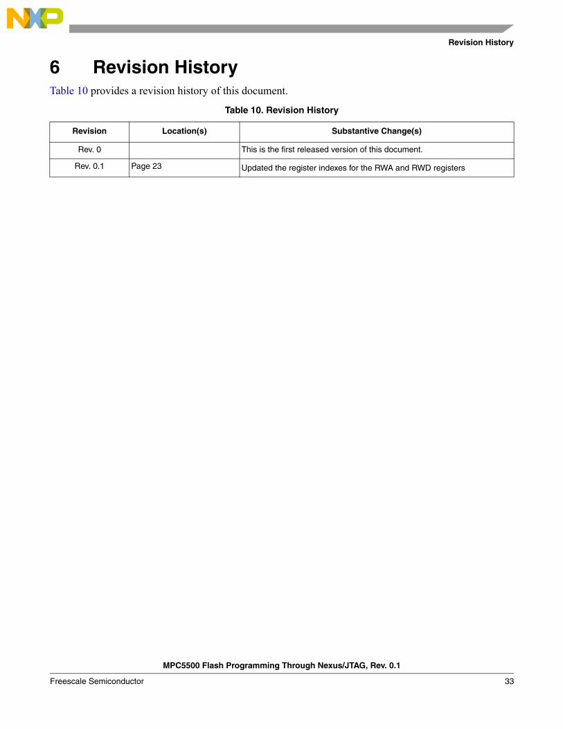
6 Revision HistoryTable 10 provides a revision history of this document.
Table 10. Revision History
Revision Location(s) Substantive Change(s)
Rev. 0 This is the first released version of this document.
Rev. 0.1 Page 23 Updated the register indexes for the RWA and RWD registers
MPC5500 Flash Programming Through Nexus/JTAG, Rev. 0.1
Freescale Semiconductor 33

How to Reach Us:
Home Page:www.freescale.com
E-mail:[email protected]
USA/Europe or Locations Not Listed:Freescale SemiconductorTechnical Information Center, CH3701300 N. Alma School RoadChandler, Arizona 85224+1-800-521-6274 or [email protected]
Europe, Middle East, and Africa:Freescale Halbleiter Deutschland GmbHTechnical Information CenterSchatzbogen 781829 Muenchen, Germany+44 1296 380 456 (English)+46 8 52200080 (English)+49 89 92103 559 (German)+33 1 69 35 48 48 (French)[email protected]
Japan:Freescale Semiconductor Japan Ltd.Technical Information Center3-20-1, Minami-Azabu, Minato-kuTokyo 106-0047, Japan0120 191014 or +81 3 3440 [email protected]
Asia/Pacific:Freescale Semiconductor Hong Kong Ltd.Technical Information Center2 Dai King StreetTai Po Industrial EstateTai Po, N.T., Hong Kong+800 2666 [email protected]
For Literature Requests Only:Freescale Semiconductor Literature Distribution CenterP.O. Box 5405Denver, Colorado 802171-800-441-2447 or 303-675-2140Fax: [email protected]
Information in this document is provided solely to enable system and software implementers to use Freescale Semiconductor products. There are no express or implied copyright licenses granted hereunder to design or fabricate any integrated circuits or integrated circuits based on the information in this document.
Freescale Semiconductor reserves the right to make changes without further notice to any products herein. Freescale Semiconductor makes no warranty, representation or guarantee regarding the suitability of its products for any particular purpose, nor does Freescale Semiconductor assume any liability arising out of the application or use of any product or circuit, and specifically disclaims any and all liability, including without limitation consequential or incidental damages. “Typical” parameters that may be provided in Freescale Semiconductor data sheets and/or specifications can and do vary in different applications and actual performance may vary over time. All operating parameters, including “Typicals”, must be validated for each customer application by customer’s technical experts. Freescale Semiconductor does not convey any license under its patent rights nor the rights of others. Freescale Semiconductor products are not designed, intended, or authorized for use as components in systems intended for surgical implant into the body, or other applications intended to support or sustain life, or for any other application in which the failure of the Freescale Semiconductor product could create a situation where personal injury or death may occur. Should Buyer purchase or use Freescale Semiconductor products for any such unintended or unauthorized application, Buyer shall indemnify and hold Freescale Semiconductor and its officers, employees, subsidiaries, affiliates, and distributors harmless against all claims, costs, damages, and expenses, and reasonable attorney fees arising out of, directly or indirectly, any claim of personal injury or death associated with such unintended or unauthorized use, even if such claim alleges that Freescale Semiconductor was negligent regarding the design or manufacture of the part.
Freescale™ and the Freescale logo are trademarks of Freescale Semiconductor, Inc. All other product or service names are the propertyof their respective owners. The ARM POWERED logo is a registered trademark of ARM Limited. ARM7TDMI-S is a trademark of ARM Limited.Java and all other Java-based marks are trademarks or registeredtrademarks of Sun Microsystems, Inc. in the U.S. and other countries.The Bluetooth trademarks are owned by their proprietor and used by Freescale Semiconductor, Inc. under license.
© Freescale Semiconductor, Inc. 2006. All rights reserved.
AN3283Rev. 0.106/2006