mpc8360e/mpc8358e powerquicc™ design checklist · the design checklist may also apply to bus- or...
TRANSCRIPT

Freescale SemiconductorApplication Note
© Freescale Semiconductor, Inc., 2007. All rights reserved.
This application note describes the generally recommended connections for new designs based on the Freescale PowerQUICC™ MPC8360E processor family. These devices include the following:
• MPC8360/E
• MPC8358/E
The design checklist may also apply to bus- or footprint-compatible processors introduced in the future. In addition, it can serve as a useful guide to debugging a newly-designed system by highlighting those areas of a design that merit special attention during initial system startup.
To locate any published errata or updates for this document, refer to the Freescale web site listed on the back cover of this document.
AN3097Rev. 1, 7/2007
Contents
1 Introduction . . . . . . . . . . . . . . . . . . . . . . . . . . . . . . . . . .22 Power . . . . . . . . . . . . . . . . . . . . . . . . . . . . . . . . . . . . . .33 Clocking. . . . . . . . . . . . . . . . . . . . . . . . . . . . . . . . . . . . 74 Power-On Reset and Reset Configurations . . . . . . . . . .95 JTAG and Debug . . . . . . . . . . . . . . . . . . . . . . . . . . . . .136 Functional Blocks . . . . . . . . . . . . . . . . . . . . . . . . . . . 177 Revision History . . . . . . . . . . . . . . . . . . . . . . . . . . . . 43
MPC8360E/MPC8358E PowerQUICC™ Design ChecklistDSD Applications
Freescale Semiconductor, Inc.

MPC8360E/MPC8358E PowerQUICC™ Design Checklist, Rev. 1
2 Freescale Semiconductor
Introduction
1 IntroductionThis section outlines recommendations to simplify the first phase of design. Before designing a system with a PowerQUICC II Pro device, it is recommended that the designer be familiar with the available documentation, software, models, and tools.
1.1 ReferencesSome of the following reference documents may be available only under a non-disclosure agreement (NDA). For those documents, contact your local field applications engineer or sales representative to obtain a copy.
• Collateral
— MPC8360E PowerQUICC™ II Pro Integrated Host processor Family Reference Manual (MPC8360ERM)
— MPC8360E PowerQUICC™ II Pro Family Device Errata (MPC8360ECE)
— MPC8360E Integrated Host Processor Hardware Specifications (MPC8360EEC)
• Available Tools
— QUICC Engine Utility Tool
— UPM Programming Tool
— Reset and Clock Programming Tool
• Models
— IBIS
— BSDL
1.2 Device ErrataThe device errata documents (MPC8360ECE) describe the latest fixes and workarounds for the MPC8360E family of devices. Before you start a design, be sure to research the most recent errata documents thoroughly.
1.3 QUICC Engine Utility ToolThe QUICC Engine utility tool is part of the NetComm driver software package available for download on the MPC8360E and MPC8358E product summary pages. The tool includes the Pin Muxing Tool, complete QUICC Engine and processor API configuration support, and the QUICC Engine Performance Calculator. The QUICC Engine Performance Calculator must be enabled with a license file.
1.4 UPM Programming ToolThe UPM programming tool features a GUI for a user-friendly programming interface through which you can program all three of the PowerQUICC II Pro UPM machines. The GUI consists of a wave editor, table editor, and report generator. The user can directly edit the waveform or the RAM array. The report generator prints out the UPM RAM array for use in a C program after programming is complete. The UPM Programming Tool is available on the MPC8360E and MPC8358E product pages of the Freescale web site.

MPC8360E/MPC8358E PowerQUICC™ Design Checklist, Rev. 1
Freescale Semiconductor 3
Power
1.5 Reset and Clock Programming ToolThe reset and clock programming tool features a Macromedia/Adobe Flash interface through which the user specifies the settings for the reset configuration word and clock settings.
1.6 Available TrainingOur third-party partners are part of an extensive Design Alliance Program. Our current training partners are listed on our web site under the Design Alliance Program. Also available are training materials from past Smart Network Developer’s Forums and Freescale Technology Forums. These training documents are a valuable resource in understanding the PowerQUICC II Pro.
1.7 Product Revisions
2 PowerThis section provides design considerations for the MPC8360E power supplies, as well as power sequencing. For information on MPC8360E AC and DC electrical specifications and thermal characteristics, refer to the MPC8360EEC. For power sequencing recommendations, refer to Section 2.3, “Power Sequencing.”
2.1 Power SupplyThe MPC8360EEC lists the recommended and maximum range for each power supply listed in Table 2. OVDD has a noise margin of 10 percent. All other power supplies have a 5 percent margin. No external signals on the MPC8360E are 5-V-tolerant. Note that absolute maximum ratings are stress ratings only. The functional operation at the maximums is not guaranteed. Stresses beyond those listed may affect device reliability or permanently damage the device.
2.2 Power DissipationThe MPC8360EEC hardware specification document provides the power dissipation of VDD for various configurations of the coherent system bus (CSB), QUICC Engine block, and the e300 core frequencies. The hardware specification also estimates power dissipation for all the I/O power rails. I/O power highly depends on the application and is an estimate. A full analysis of your board implementation is required to
Table 1. Product Revisions
Device PackageSVR
(Rev 2.0)PVR
(Rev2.0)SVR
(Rev 2.1)PVR
(Rev2.1)
MPC8360E TBGA 0x8048_0020
0x8083_0030
0x8048_0021
0x8083_0031
MPC8360 TBGA 0x8049_0020 0x8049_0021
MPC8358E TBGA 0x804A_0020 0x804A_0021
MPC8358 TBGA 0x804B_0020 0x804B_0021
MPC8358E PBGA 0x804E_0020 0x804E_0021
MPC8358 PBGA 0x804F_0020 0x804F_0021

MPC8360E/MPC8358E PowerQUICC™ Design Checklist, Rev. 1
4 Freescale Semiconductor
Power
define your I/O power supply needs. The typical VDD power plus I/O power should be used for the thermal solution design. The junction temperature must not exceed the maximum specified value. The maximum VDD power is the worst case power consumption and should be used for the core power supply design.
2.3 Power SequencingOne consequence of multiple power supplies is that when power is initially applied, the voltage rails ramp up at different rates. These rates depend on the power supply, the type of load on each power supply, and the manner in which different voltages are derived. However, advances in the PowerQUICC II Pro ESD design allow flexibility in the order in which power rails ramp, as long as the supplies do not exceed absolute maximum ratings (as defined in the hardware specification).
NOTE
From a system standpoint, if the I/O power supplies ramp before the VDD core supply stabilizes, there may be a period of time before all voltages stabilize when all functional pins, including pure input pins, are driven to a random logic-one or logic-zero state, with possible adverse effects on externally-connected logic.
The hardware specification shows the current maximum ratings for the power supplies. Supplies must not exceed these absolute maximum ratings. However, during normal operation, use the Recommended Operating Conditions tables in the hardware specification.
2.4 Power PlanesEach VDD pin should be provided with a low-impedance path to the board power supply. Similarly, each ground pin should be provided with a low-impedance path to ground. The power supply pins drive distinct groups of logic on-chip. The capacitor leads and associated printed circuit traces connecting to chip VDD and ground should be kept to less than half an inch per capacitor lead.
2.5 DecouplingDue to large address and data buses and high operating frequencies, the PowerQUICC II Pro can generate transient power surges and high-frequency noise in its power supply, especially while driving large capacitive loads. This noise must be prevented from reaching other components in the PowerQUICC II Pro system, and the PowerQUICC II Pro itself requires a clean, tightly regulated source of power. Therefore, it is recommended that the system designer place at least one decoupling capacitor at each VDD, GVDD, LVDD, OVDD pin of the PowerQUICC II Pro. These decoupling capacitors should receive their power from separate VDD, GVDD, LVDD, OVDD, and GND power planes in the PCB, using short traces to minimize inductance. Capacitors can be placed directly under the device on the other side of the board using a standard escape pattern. Others may surround the part on both top and bottom sides of the board.
These capacitors should have a value of 0.01 or 0.1 µF. Only ceramic surface mount technology (SMT) capacitors should be used to minimize lead inductance. In addition, several bulk storage capacitors should be distributed around the PCB, feeding the VDD, GVDD, LVDD, and OVDD planes, to enable quick recharging of the smaller chip capacitors. These bulk capacitors should have a low equivalent series resistance (ESR) rating to ensure the quick response time necessary. They should also be connected to the power and ground planes through two vias to minimize inductance. Suggested bulk capacitors: 100–300

MPC8360E/MPC8358E PowerQUICC™ Design Checklist, Rev. 1
Freescale Semiconductor 5
Power
µF. Simulation is strongly recommended to minimize noise on the power supplies before proceeding into the PCB design and manufacturing stage of development.
NOTE
When deciding on routing for decoupling caps, ensure that a direct connection to power and ground planes is always higher priority than the connection to the decoupling caps.
2.6 PLL Power Supply FilteringEach PowerQUICC II Pro PLL is provided with power through independent power supply pins (AVDDn). The AVDD level should always be equivalent to VDD, and preferably these voltages are derived directly from VDD through a low frequency filter scheme.
There are several ways to provide power reliably to the PLLs, but the recommended solution is four independent filter circuits as illustrated in Figure 1, one to each of the four AVDD pins. Providing independent filters to each PLL reduces the opportunity to cause noise injection from one PLL to the other. This circuit is intended to filter noise in the PLLs resonant frequency range from a 500 kHz to 10 MHz range. It should be built with surface mount capacitors with minimum effective series inductance (ESL). Consistent with the recommendations of Dr. Howard Johnson in High Speed Digital Design: A Handbook of Black Magic (Prentice Hall, 1993), multiple small capacitors of equal value are recommended over a single large value capacitor.
To minimize noise coupled from nearby circuits, each circuit should be placed as closely as possible to the specific AVDD pin being supplied. It should be possible to route directly from the capacitors to the AVDD pin, which is on the periphery of package, without the inductance of vias. Figure 1 shows the PLL power supply filter circuit.
Figure 1. PLL Power Supply Filter Circuit
2.7 Pin Listing and ConnectionsTable 2 lists the power signal pin connections.
Table 2. Power Signal Pin Listing
Signal Connection Notes
AVDD1 1.2 V ± 60 mV Power for LBIU DLL
AVDD2 1.2 V ± 60 mV Power for QUICC Engine PLL
AVDD5 1.2 V ± 60 mV Power for e300 PLL
AVDD6 1.2 V ± 60 mV Power for system PLL
GVDD 2.5 V ± 125 mV1.8 V ± 90mV
Power for DDR1 I/O voltagePower for DDR2 I/O voltage
VDD AVDDn
2.2 µF 2.2 µF
GNDLow ESL Surface Mount Capacitors
10 Ω

MPC8360E/MPC8358E PowerQUICC™ Design Checklist, Rev. 1
6 Freescale Semiconductor
Power
LVDD0 2.5 V ± 125 mV3.3 V ± 330 mV
Power for UCC1
LVDD1 2.5 V ± 125 mV3.3 V ± 330 mV
Power for UCC2 option 1
LVDD2 2.5 V ± 125 mV3.3 V ± 330 mV
Power for UCC2 option 2
VDD 1.2 V ± 60 mV or1.3 V ± 60 mV
Power for the core
OVDD 3.3 V ± 330 mV PCI, local bus, DUART, system control and power management,I2C, SPI, and JTAG I/O voltage
MVREF[1:2] 0.49 x GVDD to 0.51 x GVDD DDR I/O reference voltage
Table 2. Power Signal Pin Listing (continued)
Signal Connection Notes
MPC8360E/MPC8358E PowerQUICC™ Design Checklist, Rev. 1
Freescale Semiconductor 7
Clocking
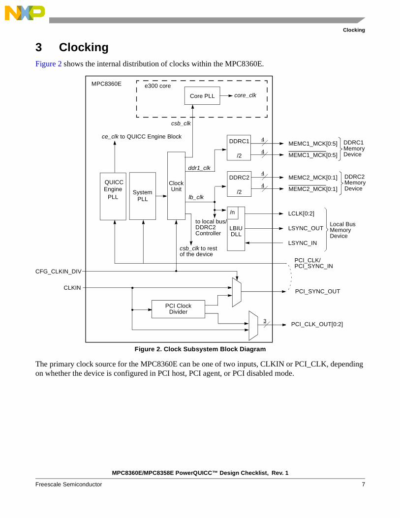
3 ClockingFigure 2 shows the internal distribution of clocks within the MPC8360E.
Figure 2. Clock Subsystem Block Diagram
The primary clock source for the MPC8360E can be one of two inputs, CLKIN or PCI_CLK, depending on whether the device is configured in PCI host, PCI agent, or PCI disabled mode.
Core PLL
System
DDRC2
LBIU
LSYNC_IN
LSYNC_OUT
LCLK[0:2]
MEMC2_MCK[0:1]
MEMC2_MCK[0:1]
core_clk
e300 core
csb_clk to rest
CLKIN
csb_clk
4
4
DDRC2Memory
Local Bus
PCI_CLK_OUT[0:2]
PCI_SYNC_OUT
PCI_CLK/
ClockUnit
of the device
lb_clk
CFG_CLKIN_DIV
PCI Clock
PCI_SYNC_IN
Device
MemoryDevice
/n
to local bus/DDRC2 Controller DLL
/2
Divider
3
MEMC1_MCK[0:5]
MEMC1_MCK[0:5]
4
4
DDRC1
/2
ddr1_clk
DDRC1MemoryDevice
PLL
QUICC
PLL
ce_clk to QUICC Engine Block
Engine
MPC8360E

MPC8360E/MPC8358E PowerQUICC™ Design Checklist, Rev. 1
8 Freescale Semiconductor
Clocking
3.1 System Clock in PCI Host ModeWhen the MPC8360E is configured as a PCI host device (RCWH[PCIHOST] = 1), CLKIN is its primary input clock. CLKIN feeds the PCI clock divider (÷2) and the PCI_SYNC_OUT and PCI_CLK_OUT multiplexers. PCI_SYNC_OUT is connected externally to PCI_SYNC_IN to allow the internal PCI controller clock to synchronize with the external PCI agent clocks. PCI_SYNC_OUT must be connected properly to PCI_SYNC_IN, with equal delay to all PCI agent devices in the system.
PCI_CLK_OUT[0:2] output buffers are enabled by RCWH[PCICKDRV]. The individual PCI_CLK_OUT[0:2] can be disabled by clearing the OCCR[PCICOEn] bit. For example, if only one PCI clock is needed, then set RCWH[PCICKDRV] and configure OCCR[0:2] = 3’b100.
CFG_CLKIN_DIV selects whether CLKIN or CLKIN÷2 is driven out on the PCI_SYNC_OUT and PCI_CLK_OUT[0:2] signals. If CFG_CLKIN_DIV = 1, then the PCI interface runs at half the CLKIN speed.
Table 3. Clock Signal Pin Listing
Signal Pin Type
ConnectionNotes
if used if not used
PCI_CLK_OUT[0:2] O As needed1 Open • Device as PCI Host: Functions as PCI output clock banks. Program the Output Clock Control Register (OCCR) to enable only the output clocks needed and disable unused clocks in order to reduce EMI.
• Device as PCI Agent or PCI Disabled: These signals are not used.
PCI_SYNC_IN/PCI_CLK
I Connect to PCI_SYNC_OUT
or25–66.67 MHz clock signals
Not applicable. This pin should
always be connected, see
Notes.
• Device as PCI Host (PCI_CLK_OUTx signals driven): Functions as PCI_SYNC_IN. Connect externally to PCI_SYNC_OUT
• Device as PCI Host (PCI_CLK_OUTx signals not driven), PCI Agent, or PCI Disabled: Functions as PCI_CLK (primary input clock to the device). A valid 25-66MHz clock signal (at OVDD level) must be applied to this signal.
PCI_SYNC_OUT O Connect to PCI_SYNC_IN
Open • Device as PCI Host (PCI_CLK_OUTx signals driven): Connect externally to PCI_SYNC_IN signal for de-skewing of external PCI clock routing. Loop trace should match with PCI_CLK_OUTx signal traces.
• Device as PCI Host (PCI_CLK_OUTx signals not driven), PCI Agent, or PCI Disabled: This signal is not used.
CLKIN I Connect to 25–66.67 MHz
clock signal
1 k-4.7 k Ω to GND
• Device as PCI Host: Functions as primary input clock. A valid 25-66MHz clock signal (at OVDD level) must be applied to this signal.
• Device as PCI Agent or PCI Disabled: This signal is not used.
Note: 1. “As needed” terminology is used throughout this document to indicate that the pin should be connected to other devices on
the board as required for the customer’s application.

MPC8360E/MPC8358E PowerQUICC™ Design Checklist, Rev. 1
Freescale Semiconductor 9
Power-On Reset and Reset Configurations
3.2 System Clock in PCI Agent ModeWhen the MPC8360E is configured as a PCI agent, PCI_CLK is the primary input clock. In agent mode, the CLKIN signal should be tied to GND. PCI_CLK_OUTn and PCI_SYNC_OUT are not used. In agent mode, the CFG_CLKIN_DIV configuration input can be used to double the internal clock frequencies.
CSB clock = PCI_CLK * (1+CFG_CLKIN_DIV) * RCWH[SPMF]
This feature is useful if a fixed internal frequency is desired, regardless of whether the PCI clock runs at 33 or 66 MHz. PCI specifications requires the PCI clock frequency information to be provided by the M66EN signal. If CFG_CLKIN_DIV=~M66EN and PCI_CLK is 33 MHz, then CSB speed is doubled.
3.3 System Clock if PCI is DisabledIf the PCI interface is not used, PCI_CLK is the primary input clock. CLKIN should be tied to GND.
3.4 VCO SettingsThe system, core, and QUICC Engine VCO values are critical to any application. The VCO dividers must be set properly as shown in Table 4. Refer to the MPC8360EEC for more information on VCO settings and suggested PLL configurations.
4 Power-On Reset and Reset ConfigurationsA detailed power-on reset flow is described in the “Reset, Clocking, and Initialization” chapter of the MPC8360E PowerQUICC™ II Pro Integrated Communications Processor Family Reference Manual.
4.1 Reset Configuration SignalsVarious device functions of the MPC8360E are initialized by sampling certain signals during the assertion of the PORESET signal after a stable clock is supplied. These inputs are either pulled high or low during this period. While these pins are generally output pins during normal operation, they are treated as inputs while PORESET is asserted. See Table 5 for termination recommendations for the reset configuration pins.
Table 4. System, Core, and QUICC Engine VCO Ranges
VCO Range (MHz)Register
Min Max
System 600 1400 RCWL[SVCOD]
Core 800 1800 RCWL[COREPLL[0:1]]
QUICC Engine 600 1400 RCWL[CEVCOD]

MPC8360E/MPC8358E PowerQUICC™ Design Checklist, Rev. 1
10 Freescale Semiconductor
Power-On Reset and Reset Configurations
The CFG_RESET_SOURCE[0:2] input signals are sampled during the assertion of PORESET to specify the interface from which the device is to load the reset configurations words. The words can be loaded from the I2C-1 interface, from a device on the local bus (CPLD, EEPROM, or FLASH), or from an internally defined word value. Table 6 describes the RCW options. For details, see the MPC8360E PowerQUICC™ II Pro Integrated Communications Processor Family Reference Manual (MPC8360ERM).
The CFG_CLKIN_DIV input signal is also sampled during the assertion of PORESET to determine the relationship between CLKIN and PCI_SYNC_IN. See Table 7. Notice that the configuration pins are multiplexed with the local bus GPLx signals. See Section 3, “Clocking.”
Table 5. Reset Configuration Pin Listing
Signal Pin Type Termination
PORESET I Driven actively by the external reset logic
HRESET I/O Pull-up with 10kΩ to OVDD
SRESET I/O Pull-up with 1.5kΩ to OVDD
LGPL0/LSDA10/ CFG_RESET_SOURCE0
I/O Pull-up with 4.7kΩ to OVDD or pull-down with 1kΩ to GND as desired, see Table 6
OR
Driven by FPGA as needed during HRESET assertion and tri-state after HRESET negation
LGPL1/LSDWE/ CFG_RESET_SOURCE1
I/O
LGPL3/LSDCAS/ CFG_RESET_SOURCE2
I/O
LGPL5/CFG_CLKIN_DIV I/O Pull-up with 4.7 kΩ to OVDD or pull-down with 1kΩ to GND as desired
Table 6. Reset Configuration Word Source
CFG_RESET_SOURCE[0:2] Value (Binary)
Description
0b000 Reset configuration words are loaded from a device on the local bus
0b001 Reset configuration words are loaded from a device on I2C-1. PCI_CLK/PCI_SYNC_IN is in the range of 25-44MHz.
Note: This option will be removed from future designs. Thus, the use of the 010 option is recommended.
0b010 Reset configuration word is loaded from a device on I2C-1. PCI_CLK/PCI_SYNC_IN is in the range of 25-66.67MHz.
0b011 - 0b111 Hard coded options 0-4.

MPC8360E/MPC8358E PowerQUICC™ Design Checklist, Rev. 1
Freescale Semiconductor 11
Power-On Reset and Reset Configurations
4.2 Reset Configuration WordsThe reset configuration words control the clock ratios and other basic device functions such as PCI host or agent mode, boot location, and endian mode. The reset configuration words are loaded from the local bus or the I2C interface during the power-on or hard reset flows. If the reset configuration word is from the flash memory, it should reside at the beginning of the flash memory. That is should start from address 0. A total of two 32-bit-words are read. The first byte is read from address 0x0, the second byte from address 0x8, the third byte from address 0x10, and so on until all 8 bytes are read. Bytes b0–b3 form a word, and this is the reset configuration word low register (RCWLR). Bytes b4–b7 form the reset configuration word high register (RCWHR):
• RCWLR
0x0000: b0xxxxxx xxxxxxxx
0x0008: b1xxxxxx xxxxxxxx
0x0010: b2xxxxxx xxxxxxxx
0x0018: b3xxxxxx xxxxxxxx
• RCWHR
0x0020: b4xxxxxx xxxxxxxx
0x0028: b5xxxxxx xxxxxxxx
0x0030: b6xxxxxx xxxxxxxx
0x0038: b7xxxxxx xxxxxxxx
If the reset configuration word is from an I2C device, the I2C setup must comply with the following requirements:
• I2C EEPROM must be connected to I2C-1.
• EEPROM of extended address type must be used.
• EEPROM must respond to the calling address 0x101_0000.
• Use the special data format as described in the reference manual.
Table 7. CLKIN Divisor Recommendations
CFG_CLKIN_DIV Value (Binary) Description
0b0 In PCI host mode: • PCI runs at CLKIN speed • csb_clk = CLKIN × SPMFIn PCI agent or PCI Disabled mode: • csb_clk = PCI_CLK × SPMF
0b1 In PCI host mode: • PCI interface runs at half of CLKIN speed • PCI_CLK_OUT = CLKIN/2 • csb_clk = (PCI_SYNC_IN × 2 × SPMF) = CLKIN × SPMFIn PCI agent or PCI Disabled mode: • csb_clk = (PCI_CLK × 2 × SPMF)

MPC8360E/MPC8358E PowerQUICC™ Design Checklist, Rev. 1
12 Freescale Semiconductor
Power-On Reset and Reset Configurations
4.2.1 Blank Flash Memory or I2C EEPROMAfter power-on reset, the MPC8360E first loads the hard reset configuration word from either the local bus or I2C device depending on the value of the CFG_RESET_SOURCE[0:2] pins.
4.2.1.1 Blank Flash Memory
If the HRCW is in the local bus flash memory, and the flash memory is blank, the MPC8360E loads an invalid HRCW and the PLL cannot lock. Therefore, the emulator cannot communicate with the device through the JTAG port. To overcome this problem, many third-party tools implement a procedure to override the HRCW through JTAG. Contact your tool vendor for further information. To override the HRCW through JTAG with CodeWarrior™, use a JTAG configuration file to change the board reset configuration settings, regardless of the current switches or the values in flash memory. The JTAG configuration file should contain the desired values for the RCWLR and RCWHR registers and specify them in the CCS remote connection settings (Debug Version Settings → Remote Debugging). You can also use the following example file:
<CW8.7_Folder>\PowerPC_EABI_Support\Initialization_Files\jtag_chains\8360_HRCW_jtag.txt
This file has one line:
E300 (1 1) (2 0x84030006) (3 0x8C600000)
The meanings of the parameters inside the JTAG configuration file are:
• Config template index 1: Boolean value that turns the overriding on and off
• Config template index 2: Value for Reset Configuration Word Low in the format of RCWLR
• Config template index 3: Value for Reset Configuration Word High in the format of RCWHR
NOTE
If index 1 is set, the next time the reset_to_user or reset_to_debug commands are issued, the core should come up with the HRCW overridden. It is not enough to clear index 1 to turn this feature off; a power-on reset should be issued.
4.2.1.2 Blank I2C EEPROM
If you are loading the HRCW from the I2C bus, the override procedure described in the previous section does not work.To avoid this situation, be sure to have an alternate means of programming the EEPROM on the I2C bus or implement an option on the board to use the default built-in HRCW options at power-on reset. The three possible workarounds are:
• Temporarily tie the SDA to the SCL pin rendering the I2C bus non-functional.
• Pull up the reset configuration pins to set the HRCW to load from a different interface such as the local bus, and then override the HRCW word.
• Pull up the reset configuration pins to use one of the default preloaded HRCW so the JTAG tool can gain control. Then program the I2C EEPROM with the appropriate HRCW.

MPC8360E/MPC8358E PowerQUICC™ Design Checklist, Rev. 1
Freescale Semiconductor 13
JTAG and Debug
4.3 Boot SequencerThe boot sequencer allows for loading the hardware reset configuration word and configuration of any memory-mapped register before the boot-up code runs. Reset configuration load mode is selected based on the settings of the CFG_RESET_SOURCE[0:2] pins during the power-on reset sequence. The I2C-1 interface loads the reset configuration words from an EEPROM at a specific calling address while the rest of the device is in the reset state. After the reset configuration words are latched inside the device, I2C-1 is reset until HRESET is negated. Then the device can be initialized using boot sequencer mode.
Boot sequencer mode is selected at power-on reset by the RCWHR[BOOTSEQ] field. The I2C module communicates with one or more EEPROMs through the I2C-1 interface to initialize one or more configuration registers of the PowerQUICC II Pro. For example, this code can be used to configure the port interface registers if the device is booting from PCI. Refer to the reference manual for the complete data format for programming the I2C EEPROM.
The boot sequencer contains a basic level of error detection. If the I2C boot sequencer fails while loading the reset configuration words, the RSR[BSF] bit is set. If a preamble or CRC fail is detected in boot sequencer mode, there is no internal or external indication that the boot sequencer operation has completed unsuccessfully.
4.4 HRESET and SRESETThe HRESET and SRESET signals are not pure input signals. They are open-drain signals that the MPC8360E processor can drive low. The connection on the left side of Figure 3 causes signal contention and must not be used.
Figure 3. HRESET and SRESET Connection
4.5 Useful System POR Debug RegistersThe hardware reset configuration settings can be read in the RCWLR, the RCWHR, the reset status register (RSR), and the system PLL mode register (SPMR). See the reference manual for details on these registers. Note that all of these resisters but the RSR are read-only registers.
5 JTAG and DebugCorrect operation of the JTAG interface requires configuration of a group of system control pins as demonstrated in Figure 5. Care must be taken to ensure that these pins are maintained at a valid negated state under normal operating conditions because most have asynchronous behavior and spurious assertion yields unpredictable results.
MPC8360 MPC8360
3.3 V 3.3 V
HRESETor
SRESET
HRESETor
SRESET
INCORRECT CORRECT

MPC8360E/MPC8358E PowerQUICC™ Design Checklist, Rev. 1
14 Freescale Semiconductor
JTAG and Debug
Boundary-scan testing is enabled through the JTAG interface signals. The TRST signal is optional in the IEEE® Std 1149.1™ specification, but it is provided on all processors that implement the PowerPC architecture. The device requires TRST to be asserted during power-on reset flow to ensure that the JTAG boundary logic does not interfere with normal chip operation. While the TAP controller can be forced to the reset state using only the TCK and TMS signals, generally systems assert TRST during the power-on reset flow. Simply tying TRST to PORESET is not practical because the JTAG interface is also used for accessing the common on-chip processor (COP), which implements the debug interface to the chip.
The COP function of these processors allow a remote computer system (typically, a PC with dedicated hardware and debugging software) to access and control the internal operations of the processor. The COP interface connects primarily through the JTAG port of the processor, with some additional status monitoring signals. The COP port requires the ability to assert PORESET and TRST independently to control the processor fully. If the target system has independent reset sources, such as voltage monitors, watchdog timers, power supply failures, or push-button switches, the COP reset signals must be merged into these signals with logic.
The arrangement shown in Figure 5 allows the COP port to assert PORESET and TRST independently, while ensuring that the target can drive PORESET as well.
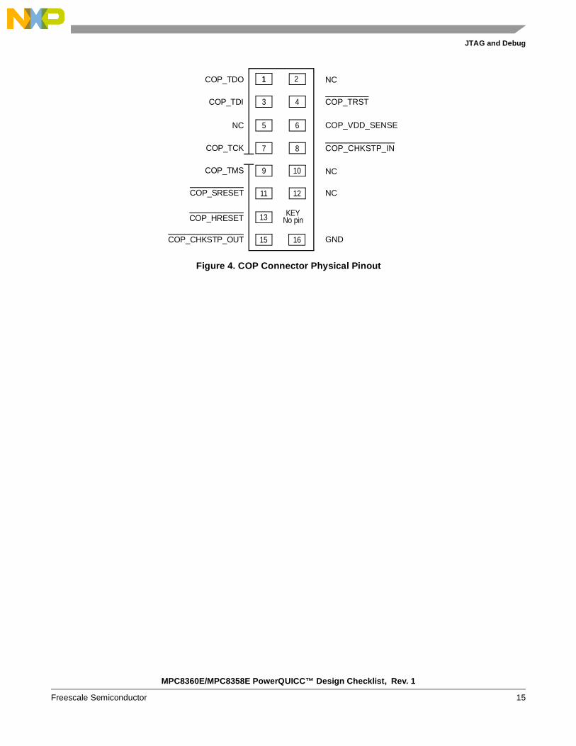
The COP interface has a standard header, shown in Figure 4, for connection to the target system, and is based on the 0.025" square-post, 0.100" centered header assembly (often called a Berg header). The connector typically has pin 14 removed as a connector key.
The COP header adds many benefits such as breakpoints, watchpoints, register and memory examination/modification, and other standard debugger features. An inexpensive option can be to leave the COP header unpopulated until needed.
There is no standardized way to number the COP header; so emulator vendors have issued many different pin numbering schemes. Some COP headers are numbered top-to-bottom then left-to-right, while others use left-to-right then top-to-bottom. Still others number the pins counter- clockwise from pin 1 (as with an IC). Regardless of the numbering scheme, the signal placement recommended in Figure 4 is common to all known emulators.
If the JTAG interface and COP header are not used, Freescale recommends all of the following connections:
• TRST should be tied to PORESET through a 0 kΩ isolation resistor so that it is asserted when the system reset signal (PORESET) is asserted, ensuring that the JTAG scan chain is initialized during the power-on reset flow. Freescale recommends that the COP header be designed into the system as shown in Figure 5. If this is not possible, the isolation resistor allows future access to TRST in case a JTAG interface may need to be wired onto the system in future debug situations.
• No pull-up/pull-down is required for TDI, TMS, TDO, or TCK.
MPC8360E/MPC8358E PowerQUICC™ Design Checklist, Rev. 1
Freescale Semiconductor 15
JTAG and Debug
Figure 4. COP Connector Physical Pinout
3
13
9
5
1
6
10
15
11
7
16
12
8
4
KEYNo pin
1 2COP_TDO
COP_TDI
NC
NC
COP_TRST
COP_VDD_SENSE
COP_CHKSTP_IN
NC
NC
GND
COP_TCK
COP_TMS
COP_SRESET
COP_HRESET
COP_CHKSTP_OUT

MPC8360E/MPC8358E PowerQUICC™ Design Checklist, Rev. 1
16 Freescale Semiconductor
JTAG and Debug
Figure 5. JTAG Interface Connection
HRESET
From TargetBoard Sources
COP_HRESET13
NC
11
COP_VDD_SENSE 26
5
15
10 Ω
10 kΩ
10 kΩ
COP_CHKSTP_INCKSTOP_IN8
COP_TMS
COP_TDO
COP_TDI
COP_TCK
TMS
TDO
TDI
9
1
3
4COP_TRST
7
16
2
10
12
(if any)
CO
P H
eade
r
14 3
Notes:
3. The KEY location (pin 14) is not physically present on the COP header.
10 kΩ
TRST 110 kΩ
10 kΩ
CKSTOP_OUTCOP_CHKSTP_OUT
3
13
9
5
1
6
10
15
11
7
16
12
8
4
KEYNo pin
COP ConnectorPhysical Pinout
1 2
NC
PORESET 1PORESET
2. Populate this with a 10 Ω resistor for short-circuit/current-limiting protection.
NC
OVDD
10 kΩ
SRESET
HRESET
processor to control the processor fully as shown here.
4. Although pin 12 is defined as a No-Connect, some debug tools may use pin 12 as an additional GND pin for
1. The COP port and target board should be able to assert PORESET and TRST independently to the
improved signal integrity.
TCK
4
This switch is included as a precaution for BSDL testing. The switch should be closed to position A during5.BSDL testing to avoid accidentally asserting the /TRST line. If BSDL testing is not being performed, this switch should be closed to position B.
5
10 kΩ
NC6
6
6. See erratum RESET3 in the MPC8360CE.
A
B
1.5 kΩ

MPC8360E/MPC8358E PowerQUICC™ Design Checklist, Rev. 1
Freescale Semiconductor 17
Functional Blocks
Table 8 details the termination recommendations for the JTAG, TEST, PMC, and thermal management pins.
6 Functional BlocksThis section discusses the recommendations and guidelines for designing with the various functional blocks on the PowerQUICC II Pro processors.
6.1 Local Bus ControllerThe local bus runs at up to 133 MHz, and it operates in either DLL bypass mode or DLL enabled mode. The frequency range for each mode is:
Table 8. JTAG and TEST Pin Listing
SignalPin
Type
TerminationNotes
If used If not used
TCK I As needed Open Commonly used for boundary scan testing. If this pin is truly not used, it can be left open.
TDI I As needed Open This JTAG pin has a weak internal pull-up P-FET that is always enabled.
TDO O As needed Open Actively driven during RESET
TMS I As needed Open This JTAG pin has a weak internal pull-up P-FET that is always enabled.
TRST I Tie to the output of a Negative
OR gate + 10 kΩ to OVDD
Tie to PORESET
through a 0 kΩ
This JTAG pin has a weak internal pull-up P-FET that is always enabled.
If an In-Circuit Emulator is used in the design, TRST should be tied to the output of a Negative OR gate logic. The inputs to the Negative OR gate logic should be any external TRST source and the PORESET signal
Test
TEST I Tie directly to GND
TEST_SEL I Tie directly to GND Applies to MPC8360/E only
TEST_SEL I Tie to GVDD Applies to MPC8358/E only
PMC
QUIESCE O As needed Open
Thermal Management
THERM0 I As needed Tie to GND1 Thermal sensitive resistor
THERM1 I As needed Tie to GND1 Thermal sensitive resistor
Note: 1. A 10 kΩ pull-down resistor may be added to these signals for testing if needed.

MPC8360E/MPC8358E PowerQUICC™ Design Checklist, Rev. 1
18 Freescale Semiconductor
Functional Blocks
• DLL bypass mode: 0–66 MHz
• DLL enable mode: 66–133 MHz
The DLL mode is controlled by LCRR[DBYP]. At 66MHz, the DLL can be programmed in either bypass mode or enable mode by LCRR[DBYP]. By default, the device powers up in DLL bypass mode by default, and the user can change the DLL mode at any time. The AC timing differs for the DLL bypass and DLL enable modes, as described in the hardware specification (MPC8360EEC).
When the DLL is enabled, LSYNC_OUT should be connected to LSYNC_IN, and the trace length between them must match the trace length between LCLKn and the external device. See Figure 8.
The local bus supports eight chip selects: LCS[0:7]. However, only LCS[0:5] are dedicated pins. LCS[6:7] are multiplexed with other function pins. The pin multiplex is controlled by SICRL[LDP_LCS_A]. There are two options:
• Option 1: LCLK[1]/LCS[6], LCLK[2]/LCS[7]
• Option 2: LDP[2]/LCS[6], LDP[3]/LCS[7]
LGPL4 must be pulled high to OVDD with a 1K-Ω resistor. In the normal case, when MPC8360E boots from the flash memory on the local bus, the local bus uses the GPCM machine. Under GPCM, the LGPL4 functions as LGTA, which is an input. Therefore, it must be pulled high. If it is floating and drifts to low, it terminates GPCM access prematurely. The pullup also avoids the issue described in the local bus signal description table in the reference manual.
The local bus frequency can be adjusted through the LCRR[CLKDIV] register field. If modified, the DLL requires a re-lock time prior to use. The lock time can vary between ~7680 and 122880 CSB clock cycles. It is a ratio between the LBC and the CSB clock. The 2:1 ratio corresponds to the minimum lock time and the 8:1 ratio corresponds to the maximum lock time. After reset, the MPC8360E defaults to a 8:1 ratio.
Software should not reconfigure the local bus clock while code is executing from the local bus, but rather while code is executing from another interface, such as the DDR controller.
6.1.1 Local Bus AddressFigure 6 shows the correct way to reconstruct the address for the local bus.
Figure 6. Local bus address
MP
C83
60 L
ocal
Bus
Inte
rfac
e
LA[0:31]
LAD[0:26]
ALE
LA[27:31]
LA[0:26]
D
Q
D
LE
Latch

MPC8360E/MPC8358E PowerQUICC™ Design Checklist, Rev. 1
Freescale Semiconductor 19
Functional Blocks
The dedicated LA[27:31] must be used to form the local address. Depending on the memory bank size, usually the address bus is less than 32 bits. For example, if the maximum memory device on the local bus is 16 Mbytes, then only 24-bit addresses are used. Only LAD[8:26] must be latched.
6.1.2 Connecting Devices to the Local BusThe MPC8360E local bus features a multiplexed address and data bus, LAD[0:31]. An external latch is required to de-multiplex these signals to the connecting device. Figure 7 shows the timing of LALE. When LALE is high, it indicates LAD[0:31] is in the address phase.
Figure 7. LALE timing
For every assertion of LCSn, LALE is asserted first. While LALE is asserted, all other control signals are negated. The duration of LALE can be programmed to 1–4 cycles in LCRR[EADC]. The default is 4 cycles. The timing of LALE negation is important to ensure the correct latch. If the change of LAD and negation of LALE are too close and the margin for the latch is not sufficient, RCWHR[LALE] can be set. LALE is negated ½ a local bus clock earlier, which should ensure enough margin.
Table 9 lists guidelines for connecting to 8-bit, 16-bit, and 32-bit devices. LAD[0] is the most significant address and data bit, and LAD[31] is the least significant address and data bit. Notice that for a 16-bit port connection, the latched address LA[31] is normally not required because byte lane control is achieved through signals as outlined in Table 9. For a 32-bit port connection, latched address LA[30:31] is normally not required. Figure 8 shows a simplified connection to a 32-bit FPGA device and a 16-bit flash memory device.
Table 9. Local Bus Byte Lane Control
Device Data Width Address DataByte Lane Control
GPCM UPM SDRAM
8-bit LA[0:31] LAD[0:7] LWE[0] LBS[0] LSDDQM[0]
16-bit LA[0:30] LAD[0:15] LWE[0:1] LBS[0:1] LSDDQM[0:1]
32-bit LA[0:29] LAD[0:31] LWE[0:3] LBS[0:3] LSDDQM[0:3]
LAD
LALE
LCSn
Address Write Data
A Latched Address
TA
LCLK

MPC8360E/MPC8358E PowerQUICC™ Design Checklist, Rev. 1
20 Freescale Semiconductor
Functional Blocks
Figure 8. Local Bus Connection to SDRAM and Flash
Table 10 shows the termination recommendations for the local bus pins.
Table 10. Local Bus Pin Listing
Cri
tica
l
SignalPin
Type
Connection
Notes
If UsedIf NotUsed
Local Bus Interface
LAD[0:31] I/O As needed 2 k–10 kΩ to OVDD
LDP[0]/ CKSTOP_OUT I/O LDP[0]: As needed
CKSTOP_OUT: As needed +
10 kΩ to OVDD
LDP[0]: 4.7 kΩ to GND
CKSTOP_OUT: Open
Pin functionality is selected by RCWH[LDP]
LDP[1]/CKSTOP_IN I/O LDP[1]: As needed
CKSTOP_IN: As needed +
10 kΩ to OVDD
LDP[1]: 4.7 kΩ to GND
CKSTOP_IN: 4.7 kΩ to OVDD
Pin functionality is selected by RCWH[LDP]
LDP[2]/LCS[6] I/O As needed Open
LDP[3]/LCS[7] I/O As needed Open
LA[27:31] O As needed Open
LCS[0:5] O As needed Open
Local Bus Interface
FPGA
Flash
LSYNC_OUT
LSYNC_IN
LCKn
Control
LA[27:31]
LALE
LBCTL
Control
A[27:31]
Control
A[23:0]
D[15:0]
Latch
QD
LE
Buffer
QD
DIR
LAD[0:26]LA[0:26]
LA[5:29]
LA[7:30]
LD[0:15]

MPC8360E/MPC8358E PowerQUICC™ Design Checklist, Rev. 1
Freescale Semiconductor 21
Functional Blocks
LWE[0:3]/LBS[0:3]/ LSDDQM[0:3]
O As needed Open
LBCTL O As needed Open
LALE O As needed Open
X LGPL0/LSDA10/ CFG_RESET_SOURCE0
I/O As needed See Table 6
X LGPL1/LSDWE/ CFG_RESET_SOURCE1
I/O As needed See Table 6
LGPL2/LSDRAS/LOE O As needed Open
X LGPL3/LSDCAS/ CFG_RESET_SOURCE2
I/O As needed See Table 6
LGPL4/LGTA/LUPWAIT/ LPBSE
I/O LPBSE: As needed
Others:As needed +1 k–10 kΩ to
OVDD
Open Pin functionality is selected by LBCR[LPBSE]
• LPBSE mode: no pullup is required. • If LGPL4 (UPM) funtionality is used,
1 kΩ to OVDD is needed. Otherwise, 10 kΩ to OVDD can be used.
X LGPL5/CFG_CLKIN_DIV I/O PCI host: 1 kΩ to OVDD or
1 kΩ to GND
PCI agent: 1 kΩ to GND
See Table 7 See Section 3, “Clocking” for details on CFG_CLKIN_DIV functionality
LCKE O As needed Open
LCLK[0] O As needed Open
LCLK[1]/LCS[6] O As needed Open
LCLK[2]/LCS[7] O As needed Open
Table 10. Local Bus Pin Listing (continued)C
riti
cal
SignalPin
Type
Connection
Notes
If UsedIf NotUsed

MPC8360E/MPC8358E PowerQUICC™ Design Checklist, Rev. 1
22 Freescale Semiconductor
Functional Blocks
6.2 DDR SDRAMRefer to the following application notes for details on layout considerations and DDR programming guidelines:
• AN2582: Hardware and Layout Design Considerations for DDR Memory Interfaces for signal integrity and layout considerations.
• AN2583: Programming the PowerQUICC III DDR SDRAM Controller.
• AN2910: Hardware and Layout Design Considerations for DDR2 SDRAM Memory Interfaces for signal integrity and layout considerations.
• AN3369: PowerQUICC DDR2 SDRAM Controller Register Setting Considerations
The MPC8360E DDR controller supports only source synchronous clock mode. Software must ensure that the DDR_SDRAM_CLK_CNTL[SS_EN] bit is set to before the DDR interface is enabled. The MPC8360E DDR controller supports both DDR1 and DDR2 SDRAM. If the DDR controller is configured for DDR2, MDIC[0] must be grounded through an 18.2-Ω precision 1 percent resistor and MDIC[1] must be connected to GVDD through an 18.2-Ω precision 1 percent resistor. These two pins are used for the automatic impedance calibration. If it is configured for DDR1, MDIC[0:1] can be left open. MODT[0:3] is for DDR2 only. If the DDR controller is configured for DDR1, MODT[0:3] can be left open.
The MPC8360E DDR controller can be configured with a 64-bit or 32-bit data bus interface. The DDR_SDRAM_CFG[32_BE] bit controls the bus width selection. The burst length should be set to 8 beats in 32-bit mode by properly configuring the DDR_SDRAM_CFG[8_BE]. Refer to the MPC8360E reference manual.
The MPC8360E DDR controller has both a primary and secondary DDR controller. If only the primary DDR controller is used, the secondary DDR controller signals can be left open. The MPC8358E features
LSYNC_OUT O DLL Bypass mode: Open or connect to LSYNC_IN with 22-33 Ω
damping resistor
DLL Enable mode: Connect to LSYNC_IN with 22-33 Ω damping
resistor
Placing a damping resistor close to the LSYNC_OUT pin is highly recommended. Simulation should be performed to verify the damping resistor value.
Trace loop from LSYNC_OUT to LSYNC_IN should go halfway out to the synchronous device (DRAM DIMM or discrete devices).LSYNC_IN I DLL Bypass mode: Tie to GND or
connect to LSYNC_OUT with 22-33 Ω damping resistor
DLL Enable mode: Connect to LSYNC_OUT with 22-33 Ω damping
resistor
Table 10. Local Bus Pin Listing (continued)C
riti
cal
SignalPin
Type
Connection
Notes
If UsedIf NotUsed

MPC8360E/MPC8358E PowerQUICC™ Design Checklist, Rev. 1
Freescale Semiconductor 23
Functional Blocks
a single DDR controller. Table 11 lists the termination recommendations for the different DDR signals for both controllers.
Table 11. DDR SDRAM Pin Listing
Cri
tical
SignalPin
Type
Connection
Notes
If UsedIf NotUsed
Primary DDR SDRAM Memory Interface
MEMC1_MDQ[0:31] I/O As needed Open When in use, proper signal integrity analysis must be performed using the respective device IBIS model.
• Parallel termination is optional for DDR signals and should be simulated to verify necessity.
• Differential termination is included on DIMMs. It is only required for discrete memory applications.
MEMC1_MDQ[32:63]/MEMC2_MDQ[0:31]
I/O As needed Open When in use, proper signal integrity analysis must be performed using the respective device IBIS model.
MEMC1_MECC[0:4]/MEMC1_MSRCID[0:4]
I/O As needed Open Pin functionality determined by SICRH[DDR] bit setting.
MEMC1_MECC[5]/MDVAL
I/O As needed Open Pin functionality determined by SICRH[DDR] bit setting.
MEMC1_MECC[6:7] I/O As needed Open
MEMC1_MDM[0:3] O As needed Open
MEMC1_MDM[4:7]/MEMC2_MDM[0:3]
O As needed Open
MEMC1_MDM[8] O As needed Open
MEMC1_MDQS[0:3] I/O As needed Open
MEMC1_MDQS[4:7]/MEMC2_MDQS[0:3]
I/O As needed Open
MEMC1_MDQS[8] I/O As needed Open
MEMC1_MBA[0:2] O As needed Open
MEMC1_MA[0:14] O As needed Open
MEMC1_MWE O As needed Open
MEMC1_MRAS O As needed Open
MEMC1_MCAS O As needed Open
MEMC1_MCS[0:3] O As needed Open
MEMC1_MCS[2:3]/MEMC2_MCS[0:1]
O
MEMC1_MCKE[0:1] O As needed Open This output is actively driven during reset rather than being three-stated during reset.
MEMC1_MCK[0:1] O As needed Open

MPC8360E/MPC8358E PowerQUICC™ Design Checklist, Rev. 1
24 Freescale Semiconductor
Functional Blocks
6.3 PCI Bus InterfacePCI_MODE is a dedicated pin that enables the PCI interface. If PCI is used, PCI_MODE must be connected to GND. All the PCI signals are multiplexed on CE_PF[4:29] and CE_PG[0:31]. If PCI is not used, PCI_MODE must have a pullup to OVDD, and CE_PF and CE_PG are free for use as other functions. Programming CE_PF[4:29] and CE_PG[0:31] to non-PCI functionality automatically terminates the PCI signals to an inactive state, and there is no need for external termination.
MEMC1_MCK[2:3]/MEMC2_MCK[0:1]
O As needed Open
MEMC1_MCK[4:5]/MEMC2_MCKE[0:1]
O As needed Open
MEMC1_MCK[0:1] O As needed Open
MEMC1_MCK[2:3]/MEMC2_MCK[0:1]
O As needed Open
MEMC1_MCK[4]/MEMC2_MDM[8]
O As needed Open
MEMC1_MCK[5]/MEMC2_MDQS[8]
O As needed Open
MEMC1_MODT[0:3] O As needed Open
MEMC1_MDIC0 I/O 18.2 Ω to GND
Open This connection is required only if DDR2 is used.
MEMC1_MDIC1 I/O 18.2 Ω to GVDD
Open This connection is required only if DDR2 is used.
Secondary DDR SDRAM Memory Interface
MEMC2_MECC[0:4]/MEMC2_MSRCID[0:4]
I/O As needed Open
MEMC2_MECC[5]/MEMC2_MDVAL
I/O As needed Open
MEMC2_MECC[6:7] I/O As needed Open
MEMC2_MBA[0:2] O As needed Open
MEMC2_MA[0:14] O As needed Open
MEMC2_MWE O As needed Open
MEMC2_MRAS O As needed Open
MEMC2_MCAS O As needed Open
Table 11. DDR SDRAM Pin Listing (continued)C
riti
cal
SignalPin
Type
Connection
Notes
If UsedIf NotUsed
MPC8360E/MPC8358E PowerQUICC™ Design Checklist, Rev. 1
Freescale Semiconductor 25
Functional Blocks
If PCI is used, program INTA/IRQ_OUT/CE_PF[5] to open drain and pull it up with a 10-kΩ resistor.
The RCWHR controls the hardware configuration of the PCI blocks as follows:
• RCWH[PCIHOST]. Host/Agent mode for PCI.
• RCWH[PCIARB]. PCI internal/external arbiter mode select.
• RCWH[PCICKDRV]. PCI clock output driver enable/disable. PCI_CLK_OUT[0:2] are multiplexed with PF[26:28]. If PCICKDRV = 1, it sets the registers that control these pins, namely CPDIR2F and CPPAR2F so that they function as output and PCI_CLK_OUT.
When the device is configured as a PCI host and PCI clock output buffers are enabled in RCWH[PCICKDRV], the device provides three clock output signals for external PCI agents, PCI_CLK_OUT[0:2]. Each clock output can be enabled (enable toggling of the clock) by setting its corresponding OCCR[PCICOEn] bit.
The MPC8360E PCI interface is hot swap friendly, meaning that it supports the hardware and software connection processes as defined in the Hot Swap specification. This level of support allows the board and system designers to build full Hot Swap systems based on the MPC8360E as a PCI target device. It is assumed that the system uses the external arbiter from the PCI host. Therefore, the extra pins needed for the CompactPCI Hot Swap are multiplexed with the PCI arbitration signals. When an external arbiter is selected (RCWH[PCIARB] = 0), the CompactPCI Hot Swap pins function. When an internal arbiter is selected (RCWH[PCIARB] = 1), the GNTx/REQx pins function.
Refer to the MPC8360E reference manual for details on the usage of the RCWH settings.
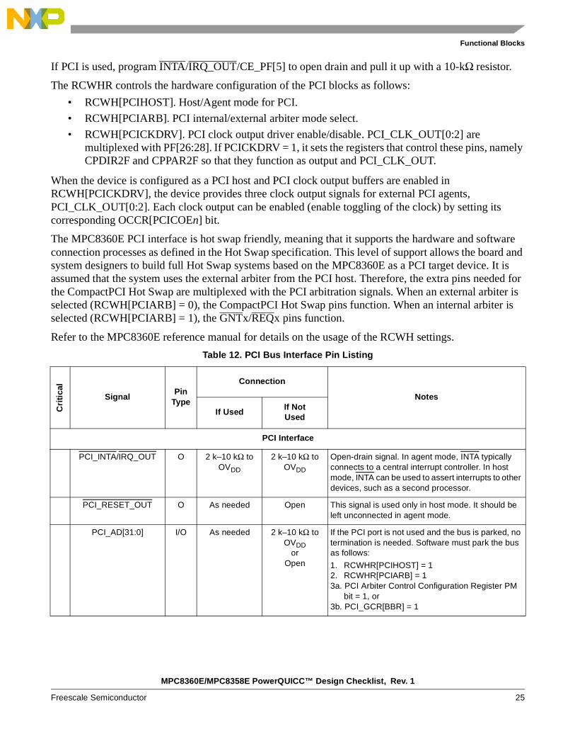
Table 12. PCI Bus Interface Pin Listing
Cri
tica
l
SignalPin
Type
Connection
Notes
If Used If NotUsed
PCI Interface
PCI_INTA/IRQ_OUT O 2 k–10 kΩ to OVDD
2 k–10 kΩ to OVDD
Open-drain signal. In agent mode, INTA typically connects to a central interrupt controller. In host mode, INTA can be used to assert interrupts to other devices, such as a second processor.
PCI_RESET_OUT O As needed Open This signal is used only in host mode. It should be left unconnected in agent mode.
PCI_AD[31:0] I/O As needed 2 k–10 kΩ to OVDD
orOpen
If the PCI port is not used and the bus is parked, no termination is needed. Software must park the bus as follows:
1. RCWHR[PCIHOST] = 12. RCWHR[PCIARB] = 13a. PCI Arbiter Control Configuration Register PM
bit = 1, or3b. PCI_GCR[BBR] = 1

MPC8360E/MPC8358E PowerQUICC™ Design Checklist, Rev. 1
26 Freescale Semiconductor
Functional Blocks
PCI_C/BE[3:0] I/O As needed +2 k–10 kΩ to
OVDD
2 k–10 kΩ to OVDD
orOpen
If the PCI port is not used and the bus is parked, no termination is needed. Software needs to park the bus as follows:
1. RCWHR[PCIHOST] = 12. RCWHR[PCI1ARB] = 13a. PCI Arbiter Control Configuration Register PM
bit = 1, or3b. PCI_GCR[BBR] = 1
PCI_PAR I/O As needed 2 k–10 kΩ to OVDD
If the PCI port is not used, this signal must be pulled up.
PCI_FRAME I/O As needed +2 k–10 kΩ to
OVDD
2 k–10 kΩ to OVDD
PCI specification requires a weak pullup.
PCI_TRDY I/O As needed +2 k–10 kΩ to
OVDD
2 k–10 kΩ to OVDD
PCI specification requires a weak pullup.
PCI_IRDY I/O As needed +2 k–10 kΩ to
OVDD
2 k–10 kΩ to OVDD
PCI specification requires a weak pullup.
PCI_STOP I/O As needed +2 k–10 kΩ to
OVDD
2 k–10 kΩ to OVDD
PCI specification requires a weak pullup.
PCI_DEVSEL I/O As needed +2 k–10 kΩ to
OVDD
2 k–10 kΩ to OVDD
PCI specification requires a weak pullup.
X PCI_IDSEL I PCI host: Tie to GND
PCI agent:One of
PCI_AD[31:0]
Tie to GND IDSEL should be connected to GND for host systems and to one address line for agent systems. If the PCI port is not used, it should be grounded.
• PCI host is selected by RCWH[PCIHOST] = 1.
• PCI agent is selected by RCWH[PCIHOST] = 0.
PCI_SERR I/O As needed +2 k–10 kΩ to
OVDD
2 k–10 kΩ to OVDD
PCI specification requires a weak pullup.
PCI_PERR I/O As needed +2 k–10 kΩ to
OVDD
2 k–10 kΩ to OVDD
PCI specification requires a weak pullup.
Table 12. PCI Bus Interface Pin Listing (continued)C
riti
cal
SignalPin
Type
Connection
Notes
If UsedIf NotUsed

MPC8360E/MPC8358E PowerQUICC™ Design Checklist, Rev. 1
Freescale Semiconductor 27
Functional Blocks
PCI_REQ0 I/O External arbiter:
As needed
Internal arbiter:
As needed +2 k–10 kΩ to
OVDD
External arbiter:Open
Internal arbiter:
2 k–10 kΩ to OVDD
If an external arbiter is used, REQ0 becomes an output signal and does not need to be terminated.
• External arbiter selected by RCWH[PCIARB] = 0. • Internal arbiter selected by RCWH[PCIARB] = 1.
PCI_REQ1/ CPCI_HS_ES
I External arbiter:
As needed
Internal arbiter:
As needed +2 k–10 kΩ to
OVDD
2 k–10 kΩ to OVDD
This pin is multiplexed with a CompactPCI Hot Swap function. CompactPCI functionality selected when external arbiter is used.
• External arbiter selected by RCWH[PCIARB] = 0. • Internal arbiter selected by RCWH[PCIARB] = 1.
PCI_REQ2 I As needed +2 k–10 kΩ to
OVDD
2 k–10 kΩ to OVDD
PCI_GNT0 I/O External arbiter:
As needed +2 k–10 kΩ to
OVDD
Internal arbiter:
As needed
External arbiter:
2 k–10 kΩ to OVDD
Internal arbiter:Open
If an external arbiter is used, GNT0 becomes an input signal and should be pulled up with 2 k–10 kΩ to OVDD.
• External arbiter selected by RCWH[PCIARB] = 0. • Internal arbiter selected by RCWH[PCIARB] = 1.
PCI_GNT1/ CPCI_HS_LED
O As needed Open This pin is multiplexed with a CompactPCI Hot Swap function. CompactPCI functionality selected when external arbiter is used.
• External arbiter selected by RCWH[PCIARB] = 0. • Internal arbiter selected by RCWH[PCIARB] = 1.
PCI_GNT2/ CPCI_HS_ENUM
O External arbiter:
As needed +2 k–10 kΩ to
OVDD
Internal arbiter:
As needed
External arbiter:Open
Internal arbiter: Open
This pin is multiplexed with a CompactPCI Hot Swap function. CompactPCI functionality selected when external arbiter is used.
• If CompactPCI Hot Swap function is used, a weak pullup is required (2 k–10 kΩ to OVDD).
• External arbiter selected by RCWH[PCIARB] = 0. • Internal arbiter selected by RCWH[PCIARB] = 1.
Table 12. PCI Bus Interface Pin Listing (continued)C
riti
cal
SignalPin
Type
Connection
Notes
If UsedIf NotUsed

MPC8360E/MPC8358E PowerQUICC™ Design Checklist, Rev. 1
28 Freescale Semiconductor
Functional Blocks
6.4 Integrated Programmable Interrupt Controller (IPIC)The integrated programmable interrupt controller (IPIC) provides interrupt management for receiving hardware-generated interrupts from different sources (both internal and external). It also prioritizes and delivers the interrupts to the CPU for servicing.
MCP_OUT is an open-drain signals that must be pulled up with a 4.7-kΩ resistor. IRQ0/MCP_IN is an input when the e300 core is enabled. When the e300 core is disabled, MCP can be used for either INTA or MCP_OUT depending on SERCR[MCPR] programming. IRQ[1:3] and IRQ[6:7] are multiplexed with other functions and are controlled by the SICRL and SICRH registers. Unused IRQ signals must be pulled up to OVDD. The LDP[1]/CKSTOP_IN and IRQ[7]/CKSTOP_IN/LCS[7] signals must be actively driven or pulled up to OVDD if they are programmed as CKSTOP_IN.
PCI_MODE O 2 k–10 kΩ to GND
2 k–10 kΩ to OVDD
M66EN I As needed 5 kΩ to OVDDor
1 kΩ to GND
No role if PCI is not used.
Table 13. Programmable Interrupt Controller Pin Listing
Cri
tica
l
SignalPin
Type
Connection
Notes
If UsedIf NotUsed
Programmable Interrupt Controller
MCP_OUT O As needed +4.7 kΩ
to OVDD
4.7 kΩ to OVDD Open drain signal
IRQ[0]/MCP_IN I As needed +2 k–10 kΩ to OVDD
2 k–10 kΩ to OVDD
IRQ[1]/M1SRCID[4]/M2SRCID[4]/LSRCID[4]
I/O As needed +2 k–10 kΩ to OVDD
2 k–10 kΩ to OVDD
Pin functionality determined by SICRL[SRCID_A] bit settings.
IRQ[2]/M1DVAL/M2DVAL/LDVAL
I/O As needed +2 k–10 kΩ to OVDD
2 k–10 kΩ to OVDD
Pin functionality determined by SICRL[SRCID_A] bit settings.
IRQ[3]/CORE_RESET I/O As needed +2 k–10 kΩ to OVDD
2 k–10 kΩ to OVDD
Pin functionality determined by SICRH[IRQ3] bit settings.
Table 12. PCI Bus Interface Pin Listing (continued)C
riti
cal
SignalPin
Type
Connection
Notes
If UsedIf NotUsed

MPC8360E/MPC8358E PowerQUICC™ Design Checklist, Rev. 1
Freescale Semiconductor 29
Functional Blocks
6.5 DUARTThe MPC8360E DUART module provides two standard UART interfaces. In addition, any UCC from the QUICC Engine block can be programmed to function as UART. Refer to Section 6.7.3, “QUICC Engine UART.” The DUART1 pins are multiplexed with the DDR Controller and Local Bus Controller debug function signals. The function is programmed with SICRL[SRCID_A]. If UART1 uses only UART1_SOUT and UART1_SIN, UART1_CTS must be pulled down.
IRQ[4:5] I As needed +2 k–10 kΩ to OVDD
2 k–10 kΩ to OVDD
IRQ[6]/LCS[6]/CKSTOP_OUT
I/O CKSTOP_OUT: As needed +
10 kΩ to OVDD
Others:As needed +
2k-10 kΩ to OVDD
CKSTOP_OUT: Open
Others: 2 k–10 kΩ to
OVDD
Pin functionality determined by SICRH[IRQ_CKSTOP_A] bit settings.
IRQ[7]/LCS[7]/CKSTOP_IN
I/O CKSTOP_IN:As needed +
10 kΩ to OVDD
Others: As needed +
2 k-10 kΩ to OVDD
CKSTOP_IN: 4.7 kΩ to OVDD
Others: 2 k–10 kΩ to
OVDD
Pin functionality determined by SICRH[IRQ_CKSTOP_A] bit settings.
Table 14. Dual UART Pin Listing
Cri
tica
l
Signal Pin Type
Connection
Notes
If UsedIf NotUsed
Dual UART
UART1_SOUT/ M1SRCID[0]/M2SRCID[0]/
LSRCID[0]
O As needed Open Pin functionality determined by SICRL[SRCID_A] bit setting.
UART1_SIN/ M1SRCID[1]/M2SRCID[1]/
LSRCID[1]
I/O As needed 2 k–10 kΩ to GND or program pin to function as
a debug pin
Pin functionality determined by SICRL[SRCID_A] bit setting.
Table 13. Programmable Interrupt Controller Pin Listing (continued)C
riti
cal
SignalPin
Type
Connection
Notes
If UsedIf NotUsed

MPC8360E/MPC8358E PowerQUICC™ Design Checklist, Rev. 1
30 Freescale Semiconductor
Functional Blocks
The pins of UART2 are multiplexed with the QUICC Engine pins. There are two options. One is on CE_PE, the other is on CE_PF. For greater flexibility, all the signals do not have to be on CE_PE or CE_PF. For example, you can assign UART2_SOUT to PE24 and UART2_SIN to PF3.
6.6 I2C InterfaceTable 16 lists the I2C pins.
UART1_CTS/ M1SRCID[2]/M2SRCID[2]/
LSRCID[2]
I/O As needed 2 k–10 kΩ to GND or program pin to function as
a debug pin
Pin functionality determined by SICRL[SRCID_A] bit setting If UART1 is used, but CTS is not used, pull it down.
UART1_RTS/ M1SRCID[3]/M2SRCID[3]/
LSRCID[3]
O As needed Open Pin functionality determined by SICRL[SRCID_A] bit setting. If UART1 is used but RTS is not used, leave open.
Table 15. DUART2 Pin Listings
SignalQUICC Engine Port
TerminationOption1 Option 2
UART2_SOUT PF0 PE24 Program to a non-UART function if the pin is not used.
UART2_SIN PF3 PE17
UART2_CTS PF1 PE23
UART2_RTS PF2 PE25
Table 16. I2C Pin Listing
SignalPin
Type
TerminationNotes
If used If not used
IIC1_SCL I/O As needed + 2k-10k Ω to OVDD
2k-10k Ω to OVDD Open-drain signal, must be pulled up
IIC1_SDA I/O As needed + 2k-10k Ω to OVDD
2k-10k Ω to OVDD Open-drain signal, must be pulled up
IIC2_SCL I/O As needed + 2k-10k Ω to OVDD
2k-10k Ω to OVDD Open-drain signal, must be pulled up
IIC2_SDA I/O As needed + 2k-10k Ω to OVDD
2k-10k Ω to OVDD Open-drain signal, must be pulled up
Table 14. Dual UART Pin Listing (continued)C
riti
cal
SignalPin
Type
Connection
Notes
If UsedIf NotUsed

MPC8360E/MPC8358E PowerQUICC™ Design Checklist, Rev. 1
Freescale Semiconductor 31
Functional Blocks
6.7 QUICC Engine Communication InterfacesThe QUICC Engine communication interfaces include the Ethernet controller, UTOPIA/POS, universal asynchronous receiver/transmitter (UART), universal serial bus (USB) controller, and serial peripheral interface (SPI).
6.7.1 Ethernet ControllerThe interfaces of the QUICC Engine are as follows:
• Media-independent interface (MII)
• Reduced media-independent interface (RMII)
• Gigabit media-independent interface (GMII)
• Reduced gigabit media-independent interface (RGMII)
• Reduced ten-bit interface (RTBI)
6.7.1.1 Media-Independent Interface (MII)
All MPC8360E UCCs can be programmed for an Ethernet protocol. We denote UCCn Ethernet as Ethernet n. All UCC Ethernets have dedicated NMSI pins that support MII interfaces, excluding the clocking signals. The NMSI signals include:
• Enet-TXD[0:3]
• Enet-TX_EN
• Enet-TX_ER
• Enet-RXD[0:3]
• Enet-COL
• Enet-CRS
• Enet-RX_DV
• Enet-RX_ER
The MPC8360E MII interface clocking pins (RX_CLK and TX_CLK) are inputs. They are driven by the PHY device. The RX_CLK and TX_CLK are routed through CLKx pins that are multiplexed with PC[0:23]. See the MPC8360E reference manual. For each Ethernet n, the RX_CLK and TX_CLK multiplexing is controlled by CMXUCRx. For Ethernet 1 and Ethernet 3, multiplexing is controlled by CMXUCR1. For Ethernet 2 and Ethernet 4, multiplexing is controlled by CMXUCR2, and so on.
6.7.1.2 RMII Interface Connection
All UCC Ethernets support the RMII interface, which uses only a subset of the MII signals. The MII signals should be connected as shown in Table 17. For RMII, the TX and RX share one clock called REF_CLK. The REF_CLK from the PHY must be connected to TX_CLK of the MPC8360E. RX_CLK is not used.

MPC8360E/MPC8358E PowerQUICC™ Design Checklist, Rev. 1
32 Freescale Semiconductor
Functional Blocks
6.7.1.3 MII/RMII Configuration
Table 18 shows all possible MII/RMII configurations. Note that these pins can also be multiplexed with other QUICC Engine functionality. Refer to the MPC8360E reference manual. The dedicated NMSI pins are denoted as “Ethn NMSI.” Notice the following:
• Ethernets 2, 4, and 5 RMII have the second option.
• Ethernet 2 RMII can pin out to the PCI/UPC2 pins, which are in the PF and PG ports.
• The Ethernet 2 secondary option is mutually exclusive with PCI/UPC2 function.
• Ethernet 4 RMII can pin out to the Ethernet 3 NMSI pins.
• The Ethernet 4 secondary option is mutually exclusive with Ethernet 3, Ethernet 1 GMII, and Ethernet 2 GMII functions.
• Ethernet 5 RMII can pin out to Ethernet 8 NMSI pins.
• The Ethernet 5 secondary option is mutually exclusive with Ethernet 8.
6.7.1.4 Gigabit Ethernet
Ethernet 1 and Ethernet 2 support Gigabit Ethernet through GMII/RGMII/TBI/RTBI.
Table 17. RMII Connection
MPC8360E Signals PHY Signals
Enet-TXD[0:1] TXD[0:1]
Enet-TX_EN TX_EN
Enet-RXD[0:1] RXD[0:1]
Enet-RX_ER RX_ER
Enet-RX_DV CRS_DV
TX_CLK REF_CLK
Table 18. MII/RMII Configuration
Ethernet Eth1-8 NMSI pins MIIRMII
Option 1 Option 2
Ethernet 1 PA[3:16] Eth1 NMSI Eth1 NMSI
Ethernet 2 PA[17:30] Eth2 NMSI Eth2 NMSI PCI/UPC2 pins
Ethernet 3 PB[0:13] Eth3 NMSI Eth3 NMSI
Ethernet 4 PB[14:27] Eth4 NMSI Eth4 NMSI Eth3 NMSI pins
Ethernet 5 PD[0:13] Eth5 NMSI Eth5 NMSI Eth8 NMSI pins
Ethernet 6 PD[14:27] Eth6 NMSI Eth6 NMSI
Ethernet 7 PE[0:13] Eth7 NMSI Eth7 NMSI
Ethernet 8 PE[14:27] Eth8 NMSI Eth8 NMSI
MPC8360E/MPC8358E PowerQUICC™ Design Checklist, Rev. 1
Freescale Semiconductor 33
Functional Blocks
GMII Data Pins
The GMII consists of the MII signals plus TXD[4:7] and RXD[4:7]. RXD[4] is multiplexed with the MII COL signal. Thus, there are seven extra data signals. The possible configuration of the pins is listed in Table 19.
Reduced Mode Interface: RGMII/RTBI
Normal port I/O voltage is 3.3 V powered by OVDD. However, RGMII and RTBI have an I/O voltage of 2.5 V. Therefore, the signals for the reduced mode are powered by LVDDx. Ethernet 1 is powered by LVDD0. Ethernet 2 RGMII has two interface options which are powered by LVDD1 and LVDD2, respectively. Table 20 lists all the pins powered by LVDDx and their functions for the RGMII and RTBI interfaces.
NOTE
Revision 2.0 silicon only supports RGMII 10/100 Mbps. See QE_ENET10 in the MPC8360ECE for more information.
Table 19. GMII Data Pins
Ethernet nGMII TXD[4:7] and RXD[5:7] pins1
Option 1 Option 2
Ethernet 1 PB[0:1], PB[4], PB[6:7], PB[9:10] PC[22:25]2
Ethernet 2 PB[2:3], PB[5], PB[8], PB[11:13]
Note: 1. PB[0:13] are also UCC3 NMSI pins. Due to pin multiplexing, use of Ethernet 1 GMII or Ethernet 2 GMII excludes use of
Ethernet 3.
2. Only TXD[4:7] have a secondary option. RXD[5:7] have no secondary option.

MPC8360E/MPC8358E PowerQUICC™ Design Checklist, Rev. 1
34 Freescale Semiconductor
Functional Blocks
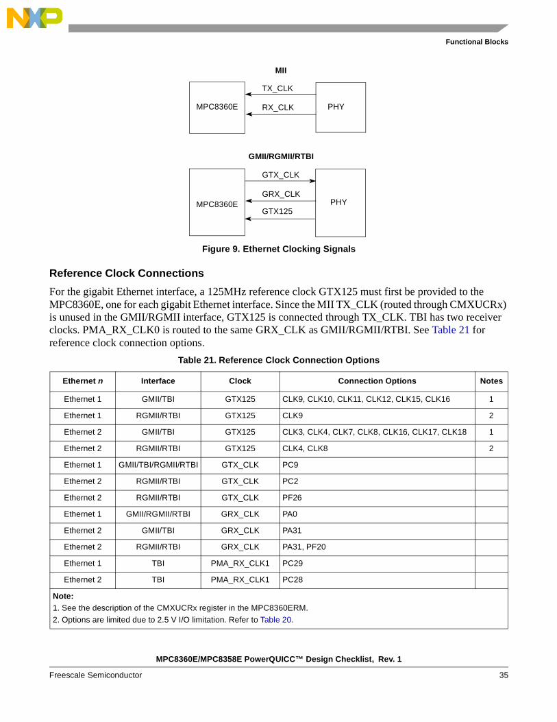
GMII/RGMII/TBI/RTBI Clocking
Clocking is responsible for much of the complexity of the gigabit Ethernet interfaces. Figure 9 shows the difference between MII clocks and GMII/RGMII clocks. For MII, both TX_CLK and RX_CLK are inputs to the MPC8360E. For gigabit Ethernet, we prefix “G” to the clock to distinguish between the interface clocks. The transmitter clock GTX_CLK is only an output for the MPC8360E.
For the MII interface, TX_CLK and RX_CLK are routed through CLK pins located in port C and controlled by CMXUCRx. Because of the high speed of the gigabit interface (125 MHz), GTX_CLK and GRX_CLK are not routed according to CMXUCRx registers. They have to be connected to dedicated pins. Gigabit Ethernet also needs the extra 125 MHz reference clock (GTX125) for its transmitter.
Table 20. Reduced Mode Power Options
Pins Powered by LVDD0 Pins Powered by LVDD1 Pins Powered by LVDD2
Port PinUCC1 RGMII
UCCRTBI
Port PinsUCC2 RGMII
UCC2RTBI
Port PinsUCC2 RGMII
UCC2RTBI
PA[0] GRX_CLK GRX_CLK PA[31] GRX_CLK GRX_CLK PF[20] GRX_CLK GRX_CLK
PA[3] TXD[0] TCG[0] PA[17] TXD[0] TCG[0] PF[5] TXD[0] TCG[0]
PA[4] TXD[1] TCG[1] PA[18] TXD[1] TCG[1] PF[6] TXD[1] TCG[1]
PA[5] TXD[2] TCG[2] PA[19] TXD[2]] TCG[2] PF[21] TXD[2] TCG[2]
PA[6] TXD[3] TCG[3] PA[20] TXD[3] TCG[3] PG[24] TXD[3] TCG[3]
PA[7] TX_EN TCG[4] PA[21] TX_EN TCG[4] PF[22] TX_EN TCG[4]
PA[9] RXD[0] RCG[0] PA[23] RXD[0] RCG[0] PF[23] RXD[0] RCG[0]
PA[10] RXD[1] RCG[1] PA[24] RXD[1] RCG[1] PF[24] RXD[1] RCG[1]
PA[11] RXD[2] RCG[2] PA[25] RXD[2] RCG[2] PG[30] RXD[2] RCG[2]
PA[12] RXD[3] RCG[3] PA[26] RXD[3] RCG[3] PF[25] RXD[3] RCG[3]
PA[15] RX_DV RCG[4] PA[29] RX_DV RCG[4] PG[31] RX_DV RCG[4]
PC[8] GTX125 GTX125 PC[3] GTX125 GTX125 PC[7] GTX125 GTX125
PC[9] GTX_CLK GTX_CLK PC[2] GTX_CLK GTX_CLK PF[26] GTX_CLK GTX_CLK
MPC8360E/MPC8358E PowerQUICC™ Design Checklist, Rev. 1
Freescale Semiconductor 35
Functional Blocks
Figure 9. Ethernet Clocking Signals
Reference Clock Connections
For the gigabit Ethernet interface, a 125MHz reference clock GTX125 must first be provided to the MPC8360E, one for each gigabit Ethernet interface. Since the MII TX_CLK (routed through CMXUCRx) is unused in the GMII/RGMII interface, GTX125 is connected through TX_CLK. TBI has two receiver clocks. PMA_RX_CLK0 is routed to the same GRX_CLK as GMII/RGMII/RTBI. See Table 21 for reference clock connection options.
Table 21. Reference Clock Connection Options
Ethernet n Interface Clock Connection Options Notes
Ethernet 1 GMII/TBI GTX125 CLK9, CLK10, CLK11, CLK12, CLK15, CLK16 1
Ethernet 1 RGMII/RTBI GTX125 CLK9 2
Ethernet 2 GMII/TBI GTX125 CLK3, CLK4, CLK7, CLK8, CLK16, CLK17, CLK18 1
Ethernet 2 RGMII/RTBI GTX125 CLK4, CLK8 2
Ethernet 1 GMII/TBI/RGMII/RTBI GTX_CLK PC9
Ethernet 2 RGMII/RTBI GTX_CLK PC2
Ethernet 2 RGMII/RTBI GTX_CLK PF26
Ethernet 1 GMII/RGMII/RTBI GRX_CLK PA0
Ethernet 2 GMII/TBI GRX_CLK PA31
Ethernet 2 RGMII/RTBI GRX_CLK PA31, PF20
Ethernet 1 TBI PMA_RX_CLK1 PC29
Ethernet 2 TBI PMA_RX_CLK1 PC28
Note: 1. See the description of the CMXUCRx register in the MPC8360ERM.
2. Options are limited due to 2.5 V I/O limitation. Refer to Table 20.
PHY
TX_CLK
RX_CLKMPC8360E
MII
PHY
GTX_CLK
GRX_CLKMPC8360E
GMII/RGMII/RTBI
GTX125

MPC8360E/MPC8358E PowerQUICC™ Design Checklist, Rev. 1
36 Freescale Semiconductor
Functional Blocks
The MPC8360E family supports programmable delay of the clock that may be used to adjust the GTX_CLK when needed. Instructions on how to program the delay for RGMII, GMII, and TBI to obtain the optimal AC timings for revision 2.1 silicon are below:
• RGMII (delaying the clock a maximum of 0.5ns if needed):
— UCC1: Write 0b10 to bits 18:19 at address IMMRBAR + 0x14A8
— UCC2 option 1: Write 0b10 to bits 4:5 at address IMMRBAR + 0x14A
— UCC2 option 2: write 0b10 to bits 16:17 at address IMMRBAR + 0x14AC
• RGMII (pulling in the clock a maximum of 0.5ns if needed):
— UCC1: Write 0b00 to bits 18:19 at address IMMRBAR + 0x14A8
— UCC2 option 1: Write 0b00 to bits 4:5 at address IMMRBAR + 0x14A8
— UCC2 option 2: Write 0b00 to bits 16:17 at address IMMRBAR + 0x14AC
• GMII (the AC timings specified in the MPC8360EEC and MPC8360ECE can be obtained only when the configuration below is performed):
— UCC1: Configure the transmit clock on CE_PC9 to CLK0 instead of GTX_CLK by setting bits 18:19 of CPPAR1C to 0b10, write 0b11 to bits 18:19 at address IMMRBAR + 0x14A8, and write 0b0000 to bits 20:23 at address IMMRBAR + 0x14AC
— UCC2: Configure the transmit clock on CE_PC2 to CLK0 instead of GTX_CLK by setting bits 4:5 of CPPAR1C to 0b11, write 0b11 to bits 4:5 at address IMMRBAR + 0x14A8, and write 0b0000 to bits 24:27 at address IMMRBAR + 0x14AC
• TBI (the AC timings specified in the MPC8360EEC and MPC8360ECE can be obtained only when the configuration below is performed):
— UCC1: Configure the transmit clock on CE_PC9 to CLK0 instead of GTX_CLK by setting bits 18:19 of CPPAR1C to 0b10, write 0b11 to bits 18:19 at address IMMRBAR + 0x14A8, and write 0b0000 to bits 20:23 at address IMMRBAR + 0x14AC
— UCC2: Configure the transmit clock on CE_PC2 to CLK0 instead of GTX_CLK by setting bits 4:5 of CPPAR1C to 0b11 and write 0b11 to bits 4:5 at address IMMRBAR + 0x14A8
TBI/RTBI Connections
Table 22 lists the TBI/RTBI connections for Ethernet 1 and Ethernet 2.
Table 22. TBI/RTBI Connections
Ethernet 1 TBI Ethernet 2 TBI
Port Pin TBI pin Port Pins TBI pin
PC9 GTX_CLK PC2 GTX_CLK
PA14 SDET PA28 SDET
PA0 RX_CLK0 PA31 RX_CLK0
PC29 RX_CLK1 PC28 RX_CLK1
PA3 TCG[0] PA17 TCG[0]
PA4 TCG[1] PA18 TCG[1]

MPC8360E/MPC8358E PowerQUICC™ Design Checklist, Rev. 1
Freescale Semiconductor 37
Functional Blocks
6.7.1.5 Speed Auto-Negotiation
This section discusses signals and connectivity when the application supports speed auto-negation and needs to switch between GMII and MII.
• GMII ↔ MII: RXD[4]/COL. Because RXD[4]/COL are multiplexed on the same signal pin and the MPC8360E supports only full duplex for gigabit Ethernet, there is no COL signal when the interface is configured for GMII. RXD[4]/COL functions as RXD[4] when the interface is configured for gigabit Ethernet. For MII, there is only RXD[0:3], so RXD[4]/COL functions as COL. For the application that supports speed auto-negotiation and needs to switch between the GMII and MII full duplex, there are no issues because MII does not need COL. However, for the special case that supports GMII and MII half duplex, RXD[4]/COL functions as RXD[4] and is connected to GMII RXD[4]. MII COL is routed to other pins as follows:
— Ethernet 1: COL is available as PC10 input SEL = 0b11 (CPPAR1C[SEL10]=0b11)
— Ethernet 2: COL is available as PC11 input SEL = 0b11 (CPPAR1C[SEL11]=0b11)
• GMII ↔ MII: RX_CLK. In the PHY device that supports GMII/MII, RX_CLK is the same signal for all the interfaces. For the MPC8360E, RX_CLK for MII and GMII are routed differently. For
PA5 TCG[2] PA19 TCG[2]
PA6 TCG[3] PA20 TCG[3]
PB6 TCG[4] PB2 TCG[4]
PB7 TCG[5] PB3 TCG[5]
PB9 TCG[6] PB5 TCG[6]
PB10 TCG[7] PB8 TCG[7]
PA7 TCG[8] PA21 TCG[8]
PA8 RCG[9] PA22 RCG[9]
PA9 RCG[0] PA23 RCG[0]
PA10 RCG[1] PA24 RCG[1]
PA11 RCG[2]] PA25 RCG[2]]
PA12 RCG[3] PA26 RCG[3]
PA13 RCG[4] PA27 RCG[4]
PB1 RCG[5] PB12 RCG[5]
PB0 RCG[6] PB13 RCG[6]
PB4 RCG[7] PB11 RCG[7]
PA15 RCG[8] PA29 RCG[8]
PA16 RCG[9] PA30 RCG[9]
Table 22. TBI/RTBI Connections (continued)
Ethernet 1 TBI Ethernet 2 TBI
Port Pin TBI pin Port Pins TBI pin
MPC8360E/MPC8358E PowerQUICC™ Design Checklist, Rev. 1
38 Freescale Semiconductor
Functional Blocks
Ethernet 1 MII, RX_CLK is from external CLK pins on PC[0:24]. For the Ethernet 1 GMII interface, GRX_CLK is always routed from PA0. For the Ethernet 2 GMII, GRX_CLK is always routed from PA31. For the Ethernet 2 MII, RX_CLK is from external CLK pins on PC[0:24]. To support both interfaces, RX_CLK of PHY devices must be connected as follows:
— Ethernet 1: Connect to PA0 and set CMXUCR1[RU1CS] = 0b1011 to choose PA0 for MII RX_CLK.
— Ethernet 2: Connect to PA31 and set CMXUCR3[RU2CS] = 0b1100 to choose PA31 for MII RX_CLK.
• GMII ↔ MII: TX_CLK and GTX125. For the GMII interface, GTX125 is connected through MII TX_CLK. When the interface switches from GMII to MII, the MII TX_CLK of the PHY device must also connect to the MPC8360E MII TX_CLK. This can be resolved by connecting GTX125 and MII TX_CLK to the different TX_CLK sources listed in CMXUCR1 and CMXUCR3, which are CLK9, CLK10, CLK11, CLK12, CLK15, and CLK16 for Ethernet 1 and CLK3, CLK4, CLK7, CLK8, CLK16, CLK17, and CLK18 for Ethernet 2. For example, if Ethernet 1 GTX125 is connected to CLK9, PHY TX_CLK can be connected to CLK10. CMXUCR1 is reprogrammed during the interface switch to pick the correct clock.
• MII/RMII ↔ TBI. Some PHY devices support both TBI and MII/RMII. They can switch between TBI and MII/RMII. The se PHYs provide the same pin for TBI RX_CLK1 and MII/RMII TX_CLK. For Ethernet 1, connect the PHY RX_CLK1/TX_CLK pin to PC29 (UCC1:TBI RX_CLK1). To use this clock for MII/RMII, configure CMXUCR1[TU1CS]=0b1011. For Ethernet 2, connect PHY RX_CLK1/TX_CLK pin to PC28 (UCC2:TBI RX_CLK1). To use this clock for MII/RMII, configure CMXUCR3[TU2CS]=0b1011.
6.7.1.6 Ethernet Management Interface
The Ethernet management interface can be controlled by a UCC or the dedicated SPI2 interface. Each UCC has its own built-in Ethernet management logic. CMXGCR[MEM] determines which UCC masters the serial management interface (SMI). SPI2 or UCC is selected in the QUICC Engine port (see Table 23). To use SPI2, program PA1 and PA2 to SPI2:MDIO and SPI2:MDC, respectively. To use the UCC management interface, program PA1 and PA2 to CE MUX:MDIO and CE MUX:MDC, respectively. The UCC selected by CMXGCR[MEM] must run in Ethernet mode to use its SMI registers. When using the UCC management interface logic instead of SPI2, you cannot use the management registers of other UCCs (for example, if the UCC1 management interface is used, the UCC2 management interface cannot be used). Section 6.7.5, “Serial Peripheral Interface (SPI),” describes how to configure SPI2 for Ethernet management.
The UCC selected by CMXGCR[MEM] must run in Ethernet mode to use its SMI registers. When using the UCC management interface logic instead of SPI2, you cannot use the management registers of other UCCs (for example, if the UCC1 management interface is used, the UCC2 management interface cannot be used).
6.7.2 UTOPIA/POSThe MPC8360E supports two UTOPIA/POS L2 interfaces. If you are familiar with the UTOPIA interface of the CPM in MPC82xx and MPC85xx, note that the external signal naming convention of the QUICC Engine block follows the UTOPIA standard. Therefore, there is different naming in master and slave

MPC8360E/MPC8358E PowerQUICC™ Design Checklist, Rev. 1
Freescale Semiconductor 39
Functional Blocks
modes. The naming conventions in the CPM retain the master mode signal naming for slave mode. For example, the QUICC Engine block transmit TXSOC in slave mode is named RXSOC, but the CPM transmit SOC in slave mode is named TXSOC. In the QUICC Engine block, you should connect signals between master and slave by name. In the example here, we connect the external master TXSOC with the QUICC Engine TXSOC.
6.7.3 QUICC Engine UARTThe MPC8360E includes a DUART; see Section 6.5, “DUART.” In addition, any UCC can be programmed to function as a UART. The QUICC Engine UART programming model is compatible with that of the CPM SCC UART. You can use the QUICC Engine UART if software backward-compatibility is important. UCC2, UCC4, and UCC5 have two pin assignment options to allow flexibility. As for UART2, it is not required that all pins be from the same option. For example, if SOUT is from option 1, SIN can be from either option 1 or option 2.
6.7.3.1 UART Configuration
The pins of the QUICC Engine UART are on each UCC NMSI interface, and they are programmed through the following registers:
• CPODRx: Determines the open-drain configuration. One bit per pin.
• CPDIR1x, CPDIR2x: Determines the in/out characteristics of the pins. Two bits per pin.
• CPPAR1x, CPPAR2x: Determines the functionality of each pin. Two bits per pin.
Table 23. QUICC Engine UART Pin Listing
UCC No.
SignalQUICC Engine Port
TerminationOption1 Option 2
UCC1 UART1_SOUT PA3/UCC1_TXD[0] If UART1 is not used, all the pins can be programmed for other functions.
If CTS is programmed for UART function but is not connected, it must be pulled low.
Programming CTS for non-UART use automatically terminates the pin to low. No pulldown resistor is needed.
UART1_SIN PA9/UCC1_RXD[0]
UART1_CTS PA15/UCC1_CTS
UART1_RTS PA7/UCC1_RTS
UCC2 UART2_SOUT PA17/UCC2_TXD[0] PF5/UCC2_TXD[0] Same as UCC1
UART2_SIN PA23/UCC2_RXD[0] PF23/UCC2_RXD[0]
UART2_CTS PA29/UCC2_CTS PG31/UCC2_CTS
UART2_RTS PA21/UCC2_RTS PF22/UCC2_RTS

MPC8360E/MPC8358E PowerQUICC™ Design Checklist, Rev. 1
40 Freescale Semiconductor
Functional Blocks
6.7.4 USB Controller
The USB controller interfaces to the USB bus through a differential line driver and differential line receiver. The OE (output enable) signal enables the line driver when the USB controller transmits on the bus. See Figure 10.
UCC3 UART3_SOUT PB0/UCC3_TXD[0] Same as UCC1
UART3_SIN PB6/UCC3_RXD[0]
UART3_CTS PB12/UCC3_CTS
UART3_RTS PB4/UCC3_RTS
UCC4 UART4_SOUT PB14/UCC4_TXD[0] PB9/UCC4_TXD[0] Same as UCC1
UART4_SIN PB20/UCC4_RXD[0] PB8/UCC4_RXD[0]
UART4_CTS PB26/UCC4_CTS PB3/UCC4_CTS
UART4_RTS PB18/UCC4_RTS PB11/UCC4_RTS
UCC5 UART5_SOUT PD0/UCC5_TXD[0] PE16/UCC5_TXD[0] Same as UCC1
UART5_SIN PD6/UCC5_RXD[0] PE22/UCC5_RXD[0]
UART5_CTS PD12/UCC5_CTS PE24/UCC5_CTS
UART5_RTS PD4/UCC5_RTS PE23/UCC5_RTS
UCC6 UART6_SOUT PD14/UCC6_TXD[0] Same as UCC1
UART6_SIN PD20/UCC6_RXD[0]
UART6_CTS PD26/UCC6_CTS
UART6_RTS PD18/UCC6_RTS
UCC7 UART7_SOUT PE0/UCC7_TXD[0] Same as UCC1
UART7_SIN PE6/UCC7_RXD[0]
UART7_CTS PE12/UCC7_CTS
UART7_RTS PE4/UCC7_RTS
UCC8 UART8_SOUT PE14/UCC8_TXD[0] Same as UCC1
UART8_SIN PE20/UCC8_RXD[0]
UART8_CTS PE26/UCC8_CTS
UART8_RTS PE18/UCC8_RTS
Table 23. QUICC Engine UART Pin Listing (continued)
UCC No.
SignalQUICC Engine Port
TerminationOption1 Option 2

MPC8360E/MPC8358E PowerQUICC™ Design Checklist, Rev. 1
Freescale Semiconductor 41
Functional Blocks
Figure 10. USB Interface
In addition, a reference clock must be provided. CMXGCR[USBCS] determines the source of USB clock. The possible clock sources are CLK3, CLK5, CLK7, CLK9, CLK13, CLK17, CLK19, CLK21, BRG9, and BRG10. The USB reference clock must be four times of the USB bit rate. Thus, it must be 48 Mhz for a 12-Mbps full-speed transfer or 6 Mhz for a 1.5-Mbps low-speed transfer.
Table 24. USB Pins and Connections
SignalQUICC Engine Port
TerminationOption1 Option 2
USB_OE PG11 PB2 If USB is not used, program these signals for general-purpose IO or other QUICC Engine functions.USB_TP PG12 PB3
USB_TN PG13 PB8
USB_RP PG5 PB9
USB_RN PF29 PB11
USB_RXD PF27 PB10
USBCLK CLK3, CLK5, CLK7, CLK9, CLK13, CLK17, CLK19, CLK21, BRG9, BRG10
USBTransceiver
QUICC Engine Block
USBRXN
USBRXP
USBRXD
USBTXN
USBTXP
USBOE

MPC8360E/MPC8358E PowerQUICC™ Design Checklist, Rev. 1
42 Freescale Semiconductor
Functional Blocks
6.7.5 Serial Peripheral Interface (SPI)The MPC8360E supports two serial peripheral interfaces (SPI). SPI2 is dedicated to Ethernet PHY management.
Table 25. SPI Pin Listing
SPI No. SignalPin
TypeQUICC Engine
Port Termination
SPI1 SPIMOSI I/O PE28 • Configure for another function if not used for SPI2. • For systems supporting SPI master and slave modes, configure to
open drain and pull up to OVDD.
SPIMISO I/O PE29 • Configure for another function if not used for SPI2 • For systems supporting SPI master and slave modes, configure to
open drain and pull up to OVDD.
SPICLK I/O PE30 • Configure for another function if not used for SPI2 • For systems supporting SPI master and slave modes, configure to
open drain and pull up to OVDD.
SPISEL I PE31 Master mode: Pullup to OVDD
Slave mode: Pulldown to GND
SPI2 MDIO I/O PA1 Configure for other function if not used for SPI2
MDC O PA2 Configure for other function if not used for SPI2

MPC8360E/MPC8358E PowerQUICC™ Design Checklist, Rev. 1
Freescale Semiconductor 43
Revision History
7 Revision History Table 26 provides a revision history for this application note.
Table 26. Document Revision History
Revision Number Date Substantive Change(s)
1 7/2007 Added overbar to INTA/IRQ_OUT/CE_PF[5] throughout
Updated binary notation to “0bnn” throughout
Updated Section 1.3, “QUICC Engine Utility Tool”Updated Table 1 with SVR and PVR information for revision 2.1 silicon
Added note to Section 2.5, “Decoupling”Updated Section 2.6, “PLL Power Supply Filtering” text to include all AVDDs. New text:
“Each PowerQUICC II Pro PLL is provided with power through independent power supply pins (AVDDn).”
Updated Figure 1 references to AVDDn
Updated Table 2:
• Removed Pin Type column because all pins are inputs • Updated AVDD2 notes to read “Power to QUICC Engine PLL” • Added GVDD power information for DDR2 • Clarified notes on OVDD and MVREF[1:2]Updated Section 3.3, “System Clock if PCI is Disabled”
Added Section 3.4, “VCO Settings” and Table 4
Added reference to Section 3, “Clocking” in Section 4.1, “Reset Configuration Signals”
Updated HRESET pull-up recommendations in Table 5 to match recommendations in Figure 5. Note that designs using the previous recommendation of a 1.5 kW pull-up on HRESET do not need to be updated.
Updated Figure 3
Updated Section 5, “JTAG and Debug”and supporting figures to reflect updated JTAG connection recommendations
Updated Table 8:
• Updated TCK termination recommendations • Added note to THERM0 and THERM1Updated Section 6.1, “Local Bus Controller” and added reference to AN3369
Clarified text in Section 6.1.1, “Local Bus Address”
Updated notes for LGPL5/CFG_CLKIN_DIV in Table 10
Corrected Figure 6 to reference LA[27:31]
Updated Section 6.4, “Integrated Programmable Interrupt Controller (IPIC)” text read:“When the e300 core is disabled, MCP can be used for either INTA or MCP_OUT depending on SERCR[MCPR] programming.”
Clarified text in Section 6.5, “DUART”:“The DUART1 pins are multiplexed with the DDR Controller and Local Bus Controller debug function signals.”
Added note to Section , “Reduced Mode Interface: RGMII/RTBI”
Added RGMII, GMII, and TBI clock programming recommendations to Section , “GMII/RGMII/TBI/RTBI Clocking”
Updated notes in Table 21 to read:
“1. See the description of the CMXUCRx register in the MPC8360ERM. 2. Options are limited due to 2.5 V I/O limitation. Refer to Table 20.”
Updated Section 6.7.1.6, “Ethernet Management Interface”
Added CLK13 as USB clock option in Section 6.7.4, “USB Controller” and Table 24
0 9/2006 Initial release.

Document Number: AN3097Rev. 17/2007
Freescale™ and the Freescale logo are trademarks of Freescale Semiconductor, Inc. The Power Architecture and Power.org word marks and the Power and Power.org logos and related marks are trademarks and service marks licensed by Power.org. All other product or service names are the property of their respective owners.
© Freescale Semiconductor, Inc., 2004, 2007.
Information in this document is provided solely to enable system and software
implementers to use Freescale Semiconductor products. There are no express or
implied copyright licenses granted hereunder to design or fabricate any integrated
circuits or integrated circuits based on the information in this document.
Freescale Semiconductor reserves the right to make changes without further notice to
any products herein. Freescale Semiconductor makes no warranty, representation or
guarantee regarding the suitability of its products for any particular purpose, nor does
Freescale Semiconductor assume any liability arising out of the application or use of
any product or circuit, and specifically disclaims any and all liability, including without
limitation consequential or incidental damages. “Typical” parameters which may be
provided in Freescale Semiconductor data sheets and/or specifications can and do
vary in different applications and actual performance may vary over time. All operating
parameters, including “Typicals” must be validated for each customer application by
customer’s technical experts. Freescale Semiconductor does not convey any license
under its patent rights nor the rights of others. Freescale Semiconductor products are
not designed, intended, or authorized for use as components in systems intended for
surgical implant into the body, or other applications intended to support or sustain life,
or for any other application in which the failure of the Freescale Semiconductor product
could create a situation where personal injury or death may occur. Should Buyer
purchase or use Freescale Semiconductor products for any such unintended or
unauthorized application, Buyer shall indemnify and hold Freescale Semiconductor
and its officers, employees, subsidiaries, affiliates, and distributors harmless against all
claims, costs, damages, and expenses, and reasonable attorney fees arising out of,
directly or indirectly, any claim of personal injury or death associated with such
unintended or unauthorized use, even if such claim alleges that Freescale
Semiconductor was negligent regarding the design or manufacture of the part.
How to Reach Us:
Home Page: www.freescale.com
email: [email protected]
USA/Europe or Locations Not Listed: Freescale Semiconductor Technical Information Center, CH3701300 N. Alma School Road Chandler, Arizona 85224 [email protected]
Europe, Middle East, and Africa:Freescale Halbleiter Deutschland GmbHTechnical Information CenterSchatzbogen 781829 Muenchen, Germany+44 1296 380 456 (English) +46 8 52200080 (English)+49 89 92103 559 (German)+33 1 69 35 48 48 (French) [email protected]
Japan: Freescale Semiconductor Japan Ltd. HeadquartersARCO Tower 15F1-8-1, Shimo-Meguro, Meguro-ku Tokyo 153-0064, Japan 0120 191014+81 3 5437 [email protected]
Asia/Pacific: Freescale Semiconductor Hong Kong Ltd. Technical Information Center2 Dai King Street Tai Po Industrial Estate, Tai Po, N.T., Hong Kong +800 2666 [email protected]
For Literature Requests Only:Freescale Semiconductor
Literature Distribution Center P.O. Box 5405Denver, Colorado 80217 1-800-441-2447303-675-2140Fax: 303-675-2150LDCForFreescaleSemiconductor
@hibbertgroup.com