mpq4488 36v, 6a, step-down converter with programmable
TRANSCRIPT

MPQ4488 36V, 6A, Step-Down Converter with
Programmable Frequency and Spread Spectrum Option, Dual USB Charging Ports
Supporting DCP and Type-C 5V @ 3A DFP Mode for Automotive, AEC-Q100 Qualified
MPQ4488 Rev. 1.0 www.MonolithicPower.com 1 10/17/2017 MPS Proprietary Information. Patent Protected. Unauthorized Photocopy and Duplication Prohibited. Prelim © 2017 MPS. All Rights Reserved.
The Future of Analog IC Technology
DESCRIPTION The MPQ4488 integrates a monolithic, step-down, switch-mode converter with two USB current-limit switches and charging port identification circuitry for each port. The MPQ4488 achieves 6A of output current with excellent load and line regulation over a wide input supply range.
The output of each USB switch is current-limited. Both USB ports support DCP schemes for battery charging specification (BC1.2), divider mode, 1.2V/1.2V mode, and USB Type-C 5V @ 3A DFP mode, eliminating the need for outside user interaction.
Full protection features include hiccup current limiting, output over-voltage protection (OVP), and thermal shutdown.
The MPQ4488 requires a minimal number of readily available, standard, external components and is available in a QFN-26 (5mmx5mm) package.
FEATURES Wide 6V to 36V Operating Input Voltage
Range Selectable Output Voltage: 5.1V, 5.17V, and
5.3V 90mV Line Drop Compensation Accurate USB1/USB2 Output-Current Limit 18mΩ/15mΩ Low RDS(ON) Internal Buck
Power MOSFETs 18mΩ/18mΩ Low RDS(ON) Internal
USB1/USB2 Power MOSFETs Frequency Adjustable (250kHz to 2.2MHz) Frequency Spread Spectrum for
MPQ4488GU-FD-AEC1 Forced CCM Operation Load Shedding versus Temperature Hiccup Current Limit for both Buck and USB Supports DCP Schemes for BC1.2, Divider
Mode, and 1.2V/1.2V Mode Supports USB Type-C 5V @ 3A DFP Mode ±8kV HBM ESD Rating for USB, DP, and
DM Available in a QFN-26 (5mmx5mm)
Package Available in AEC-Q100 Grade 1
APPLICATIONS USB Dedicated Charging Ports (DCP) USB Type-C Charging Port All MPS parts are lead-free, halogen-free, and adhere to the RoHS directive. ForMPS green status, please visit the MPS website under Quality Assurance. “MPS” and “The Future of Analog IC Technology” are registered trademarks of Monolithic Power Systems, Inc.

MPQ4488 – STEP-DOWN CONVERTER W/ DUAL USB CHARGING PORTS FOR AUTO, AEC-Q100 QUALIFIED
MPQ4488 Rev. 1.0 www.MonolithicPower.com 2 10/17/2017 MPS Proprietary Information. Patent Protected. Unauthorized Photocopy and Duplication Prohibited. Preliminary Specifications Subject to Change © 2017 MPS. All Rights Reserved.
TYPICAL APPLICATION
80
84
88
92
96
100
0 1 2 3 4 5 6 7

MPQ4488 – STEP-DOWN CONVERTER W/ DUAL USB CHARGING PORTS FOR AUTO, AEC-Q100 QUALIFIED
MPQ4488 Rev. 1.0 www.MonolithicPower.com 3 10/17/2017 MPS Proprietary Information. Patent Protected. Unauthorized Photocopy and Duplication Prohibited. Prelim © 2017 MPS. All Rights Reserved.
ORDERING INFORMATION Part Number* Package Top Marking
MPQ4488GU-AEC1 QFN-26 (5mmx5mm) See Below
MPQ4488GU-FD-AEC1
* For Tape & Reel, add suffix –Z (e.g. MPQ4488GU-AEC1–Z, MPQ4488GU-FD-AEC1–Z)
DEVICE COMPARISON INFORMATION Part Number Frequency Spread Spectrum
MPQ4488GU-AEC1 No MPQ4488GU-FD-AEC1 Yes
TOP MARKING
MPS: MPS prefix YY: Year code WW: Week code MP4488: Product code of MPQ4488GU-AEC1 and MPQ4488GU-FD-AEC1 LLLLLLL: Lot number
PACKAGE REFERENCE
TOP VIEW
QFN-26 (5mmx5mm)

MPQ4488 – STEP-DOWN CONVERTER W/ DUAL USB CHARGING PORTS FOR AUTO, AEC-Q100 QUALIFIED
MPQ4488 Rev. 1.0 www.MonolithicPower.com 4 10/17/2017 MPS Proprietary Information. Patent Protected. Unauthorized Photocopy and Duplication Prohibited. Prelim © 2017 MPS. All Rights Reserved.
ABSOLUTE MAXIMUM RATINGS (1) Supply voltage (VIN) ...................... -0.4V to +40V VSW .................................... -0.3V (-5V for <10ns) to VIN + 0.3V (43V for <10ns) VBST ................................................... VSW + 5.5V VEN ............................................ -0.3V to +10V (2)
VOUT, VUSB ..................................... -0.3V to +6.5V All other pins ................................ -0.3V to +5.5V
Continuous power dissipation (TA = +25°C) (3)
QFN-26 (5mmx5mm) ............................... 6.25W Junction temperature ................................ 150°C Lead temperature ..................................... 260°C Storage temperature ................ -65°C to +150°C
Recommended Operating Conditions (4) Operation input voltage range ............ 6V to 36V Output current ........... 3A for USB1, 3A for USB2 Operating junction temp. (TJ) ... -40°C to +125°C
Thermal Resistance θJA θJC QFN-26 (5mmx5mm)
JESD51-7 (5)
.......................... 44 ........ 9 .... °C/W 4-Layer PCB 50mmx50mm ... 20 ........ 2 .... °C/W
NOTES: 1) Absolute maximum ratings are rated under room temperature
unless otherwise noted. Exceeding these ratings may damage the device.
2) For details on EN’s ABS Max rating, refer to the EN Control section on page 12.
3) The maximum allowable power dissipation is a function of the maximum junction temperature TJ (MAX), the junction-to-ambient thermal resistance θJA, and the ambient temperature TA. The maximum allowable continuous power dissipation at any ambient temperature is calculated by PD (MAX) = (TJ
(MAX)-TA)/θJA. Exceeding the maximum allowable power dissipation will cause excessive die temperature, and the regulator will go into thermal shutdown. Internal thermal shutdown circuitry protects the device from permanent damage. Measured on 4-layer PCB (50mmx50mm).
4) The device is not guaranteed to function outside of its operating conditions.
5) Measured on JESD51-7, 4-layer PCB.
MPQ4488 – STEP-DOWN CONVERTER W/ DUAL USB CHARGING PORTS FOR AUTO, AEC-Q100 QUALIFIED
MPQ4488 Rev. 1.0 www.MonolithicPower.com 5 10/17/2017 MPS Proprietary Information. Patent Protected. Unauthorized Photocopy and Duplication Prohibited. Prelim © 2017 MPS. All Rights Reserved.
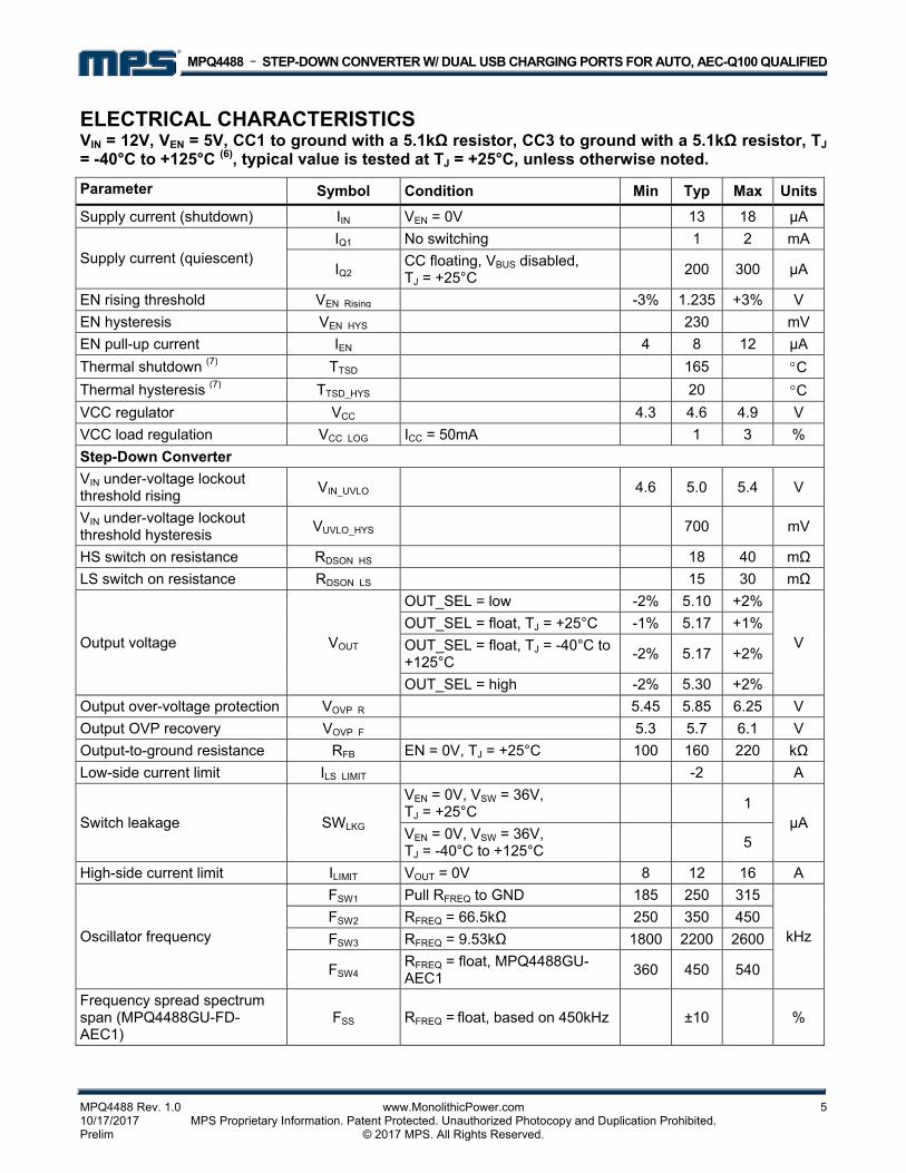
ELECTRICAL CHARACTERISTICS VIN = 12V, VEN = 5V, CC1 to ground with a 5.1kΩ resistor, CC3 to ground with a 5.1kΩ resistor, TJ = -40°C to +125°C (6), typical value is tested at TJ = +25°C, unless otherwise noted.
Parameter Symbol Condition Min Typ Max Units
Supply current (shutdown) IIN VEN = 0V 13 18 μA
Supply current (quiescent) IQ1 No switching 1 2 mA
IQ2 CC floating, VBUS disabled, TJ = +25°C
200 300 μA
EN rising threshold VEN Rising -3% 1.235 +3% V
EN hysteresis VEN HYS 230 mV
EN pull-up current IEN 4 8 12 μA
Thermal shutdown (7) TTSD 165 C
Thermal hysteresis (7) TTSD_HYS 20 C
VCC regulator VCC 4.3 4.6 4.9 V
VCC load regulation VCC LOG ICC = 50mA 1 3 %
Step-Down Converter
VIN under-voltage lockout threshold rising
VIN_UVLO 4.6 5.0 5.4 V
VIN under-voltage lockout threshold hysteresis
VUVLO_HYS 700 mV
HS switch on resistance RDSON HS 18 40 mΩ
LS switch on resistance RDSON LS 15 30 mΩ
Output voltage VOUT
OUT_SEL = low -2% 5.10 +2%
V
OUT_SEL = float, TJ = +25°C -1% 5.17 +1%
OUT_SEL = float, TJ = -40°C to +125°C
-2% 5.17 +2%
OUT_SEL = high -2% 5.30 +2%
Output over-voltage protection VOVP R 5.45 5.85 6.25 V
Output OVP recovery VOVP F 5.3 5.7 6.1 V
Output-to-ground resistance RFB EN = 0V, TJ = +25°C 100 160 220 kΩ
Low-side current limit ILS LIMIT -2 A
Switch leakage SWLKG
VEN = 0V, VSW = 36V, TJ = +25°C
1 μA
VEN = 0V, VSW = 36V, TJ = -40°C to +125°C
5
High-side current limit ILIMIT VOUT = 0V 8 12 16 A
Oscillator frequency
FSW1 Pull RFREQ to GND 185 250 315
kHzFSW2 RFREQ = 66.5kΩ 250 350 450
FSW3 RFREQ = 9.53kΩ 1800 2200 2600
FSW4 RFREQ = float, MPQ4488GU-AEC1
360 450 540
Frequency spread spectrum span (MPQ4488GU-FD-AEC1)
FSS RFREQ = float, based on 450kHz ±10 %

MPQ4488 – STEP-DOWN CONVERTER W/ DUAL USB CHARGING PORTS FOR AUTO, AEC-Q100 QUALIFIED
MPQ4488 Rev. 1.0 www.MonolithicPower.com 6 10/17/2017 MPS Proprietary Information. Patent Protected. Unauthorized Photocopy and Duplication Prohibited. Prelim © 2017 MPS. All Rights Reserved.
ELECTRICAL CHARACTERISTICS (continued) VIN = 12V, VEN = 5V, CC1 to ground with 5.1kΩ resistor, CC3 to ground with a 5.1kΩ resistor, TJ = -40°C to +125°C (6), typical value is tested at TJ = +25°C, unless otherwise noted.
Parameter Symbol Condition Min Typ Max Units
Maximum duty cycle DMAX FREQ = 450kHz 91 95 99 %
Minimum off time TOFF MIN 110 ns
Minimum on time(7) TON_MIN 130 ns
Soft-start time TSS Output from 10% to 90% 1 2 3.4 ms
USB Switch (USB1 and USB2)
Under-voltage lockout threshold rising
VUSB_UVR 3.7 4 4.3 V
Under-voltage lockout threshold hysteresis
VUSB_UVHYS 200 mV
Switch on resistance RDSON SW 18 35 mΩ
Output discharge resistance RDIS_USB Apply 5V voltage on USB output, CC floating
250 500 750 kΩ
USB OVP clamp VUSB OV 5.3 5.6 5.9 V
Current limit ILimit1
VOUT drops 10%, Type-C mode, TJ = +25°C
-6% 3.55 6% A
ILimit2 VOUT drops 10%, Type-A mode, TJ = +25°C
2.6 2.75 2.9
Line drop compensation VDROP COM IOUT = 2.4A, VOUT = 5.17V 40 90 140 mV
VBUS soft-start time TSS Output from 10% to 90% 1 2 3 ms
Hiccup mode on time THICP_ON2
OC, VOUT drops 10%, TJ = +25°C
3.5 5 6.5 ms
OC, VOUT drops 10%, TJ = -40°C to +125°C
3 5 7
Hiccup mode off time THICP OFF VOUT connected to GND 1 2 3 s
BC1.2 DCP Mode
DP and DM short resistance RDP/DM_Short
VDP = 0.8V, IDM = 1mA, TJ = +25°C
85 155Ω
VDP = 0.8V, IDM = 1mA, TJ = -40°C to +125°C
85 160
Divider Mode
DP/DM output voltage VDP/DM Divider 2.55 2.7 2.85 V
DP/DM output impedance RDP/DM_Divider TJ = +25°C 14 22 30
kΩ TJ = -40°C to +125°C 12 22 34
1.2V/1.2V Mode
DP/DM output voltage VDP/DM_1.2V VOUT = 5V, TJ = +25°C 1.12 1.2 1.28
V VOUT = 5V, TJ = -40°C to +125°C
1.1 1.2 1.3
DP/DM output impedance RDP/DM_1.2V TJ = +25°C 70 105 140
kΩ TJ = -40°C to +125°C 60 105 150

MPQ4488 – STEP-DOWN CONVERTER W/ DUAL USB CHARGING PORTS FOR AUTO, AEC-Q100 QUALIFIED
MPQ4488 Rev. 1.0 www.MonolithicPower.com 7 10/17/2017 MPS Proprietary Information. Patent Protected. Unauthorized Photocopy and Duplication Prohibited. Prelim © 2017 MPS. All Rights Reserved.
ELECTRICAL CHARACTERISTICS (continued) VIN = 12V, VEN = 5V, CC1 to ground with a 5.1kΩ resistor, CC3 to ground with a 5.1kΩ resistor, TJ = -40°C to +125°C(6), Typical value is tested at TJ = +25°C, unless otherwise noted.
Parameter Symbol Condition Min Typ Max Units
USB Type-C 5V @ 3A Mode – CC1, CC2, CC3 and CC4
CC resistor to disable Type-C mode
RA
CC1 and CC3 pins, for Type-C mode application, a 1nF capacitor should be added on CC1 and CC3 respectively
70 90 kΩ
CC voltage to enable VCONN VRa 0.75 V
CC voltage to enable VBUS VRd 0.9 2.45 V
CC detach threshold VOPEN 2.75 V
CC voltage falling debounce timer
TCC_debounce VBUS enable deglitch 100 144 200 ms
CC voltage rising debounce timer
TPD_debounce VBUS disable deglitch 10 15 20 ms
VCONN output power PVCONN
VCONN comes from buck output with some series resistance, for applications without SuperSpeed data.
100 mW
NOTES: 6) All min/max parameters are tested at TJ = 25°C. Limits over temperature are guaranteed by design, characterization, and correlation. 7) Guaranteed by design and characterization test.

MPQ4488 – STEP-DOWN CONVERTER W/ DUAL USB CHARGING PORTS FOR AUTO, AEC-Q100 QUALIFIED
MPQ4488 Rev. 1.0 www.MonolithicPower.com 8 10/17/2017 MPS Proprietary Information. Patent Protected. Unauthorized Photocopy and Duplication Prohibited. Prelim © 2017 MPS. All Rights Reserved.
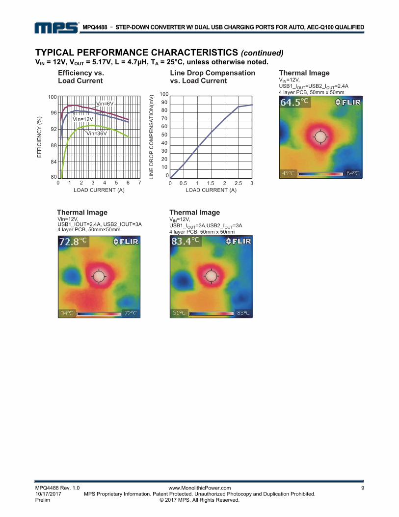
TYPICAL PERFORMANCE CHARACTERISTICS VIN = 12V, VOUT = 5.17V, L = 4.7µH, TA = 25°C, unless otherwise noted.
MPQ4488 – STEP-DOWN CONVERTER W/ DUAL USB CHARGING PORTS FOR AUTO, AEC-Q100 QUALIFIED
MPQ4488 Rev. 1.0 www.MonolithicPower.com 9 10/17/2017 MPS Proprietary Information. Patent Protected. Unauthorized Photocopy and Duplication Prohibited. Prelim © 2017 MPS. All Rights Reserved.
TYPICAL PERFORMANCE CHARACTERISTICS (continued) VIN = 12V, VOUT = 5.17V, L = 4.7µH, TA = 25°C, unless otherwise noted.
80
84
88
92
96
100
0 1 2 3 4 5 6 7
0
10
20
30
40
50
60
70
80
90
100
0 0.5 1 1.5 2 2.5 3

MPQ4488 – STEP-DOWN CONVERTER W/ DUAL USB CHARGING PORTS FOR AUTO, AEC-Q100 QUALIFIED
MPQ4488 Rev. 1.0 www.MonolithicPower.com 10 10/17/2017 MPS Proprietary Information. Patent Protected. Unauthorized Photocopy and Duplication Prohibited. Prelim © 2017 MPS. All Rights Reserved.
PIN FUNCTIONS QFN 5x5
Pin # Name Description
1 CC1 Configuration channel. CC1 is used to detect connections and configure the interface across the USB1 Type-C cables and connectors. Once a connection is established, CC1 or CC2 is reassigned to provide power over the VCONN of the plug.
2 USB1 USB1 output.
3, 15, 25 OUT Buck output. OUT is the power input for USB1 and USB2.
4, 14 IN
Supply voltage. IN is the drain of the internal power device and provides the power supply for the entire chip. The MPQ4488 operates from a 6V to 36V input voltage. A capacitor (CIN) prevents large voltage spikes at the input. Place CIN as close to the IC as possible.
5, 13 PGND Power ground. PGND is the reference ground of the regulated output voltage. PGND requires careful consideration during the PCB layout. Connect PGND with copper traces and vias.
6 AGND Analog ground. Connect AGND to PGND.
7 VCC Internal 4.6V LDO regulator output. Decouple VCC with a 1µF capacitor.
8, 9, 26 SW Switch output. Use a wide PCB trace to make the connection.
10 BST Bootstrap. A 0.22µF capacitor is connected between SW and BST to form a floating supply across the high-side switch driver.
11 OUT_SEL Buck output voltage set. Setting OUT_SEL to either a low, floating, or high connection can set three different output voltages (5.1V, 5.17V, 5.3V).
12 FREQ
Switching frequency program input. For the MPQ4488GU-AEC1, connect a resistor from FREQ to GND to set the switching frequency. Float FREQ or connect FREQ to VCC to achieve a 450kHz frequency. Connect FREQ to ground to achieve a 250kHz internal frequency.
For the MPQ4488GU-FD-AEC1, float FREQ or connect FREQ to VCC to achieve a ±10% frequency spread spectrum based on 450kHz. Connect a resistor from FREQ to GND or pull FREQ to GND to set the switching frequency without a frequency spread spectrum.
16 USB2 USB2 output.
17 CC4 Configuration channel. CC4 is used to detect connections and configure the interface across the USB2 Type-C cables and connectors. Once a connection is established, CC3 or CC4 is reassigned to provide power over the VCONN of the plug.
18 CC3 Configuration channel. CC3 is used to detect connections and configure the interface across the USB2 Type-C cables and connectors. Once a connection is established, CC3 or CC4 is reassigned to provide power over the VCONN of the plug.
19 DM2 D- data line to USB2 connector. The input/output is used for handshaking with portable devices.
20 DP2 D+ data line to USB2 connector. The input/output is used for handshaking withportable devices.
21 EN On/off control input. EN has an internal auto pull-up with an 8µA current source.
22 DP1 D+ data line to USB1 connector. The input/output is used for handshaking with portable devices.
23 DM1 D- data line to USB1 connector. The input/output is used for handshaking with portable devices.
24 CC2 Configuration channel. CC2 is used to detect connections and configure the interface across the USB1 Type-C cables and connectors. Once a connection is established, CC1 or CC2 is reassigned to provide power over the VCONN of the plug.
MPQ4488 – STEP-DOWN CONVERTER W/ DUAL USB CHARGING PORTS FOR AUTO, AEC-Q100 QUALIFIED
MPQ4488 Rev. 1.0 www.MonolithicPower.com 11 10/17/2017 MPS Proprietary Information. Patent Protected. Unauthorized Photocopy and Duplication Prohibited. Prelim © 2017 MPS. All Rights Reserved.
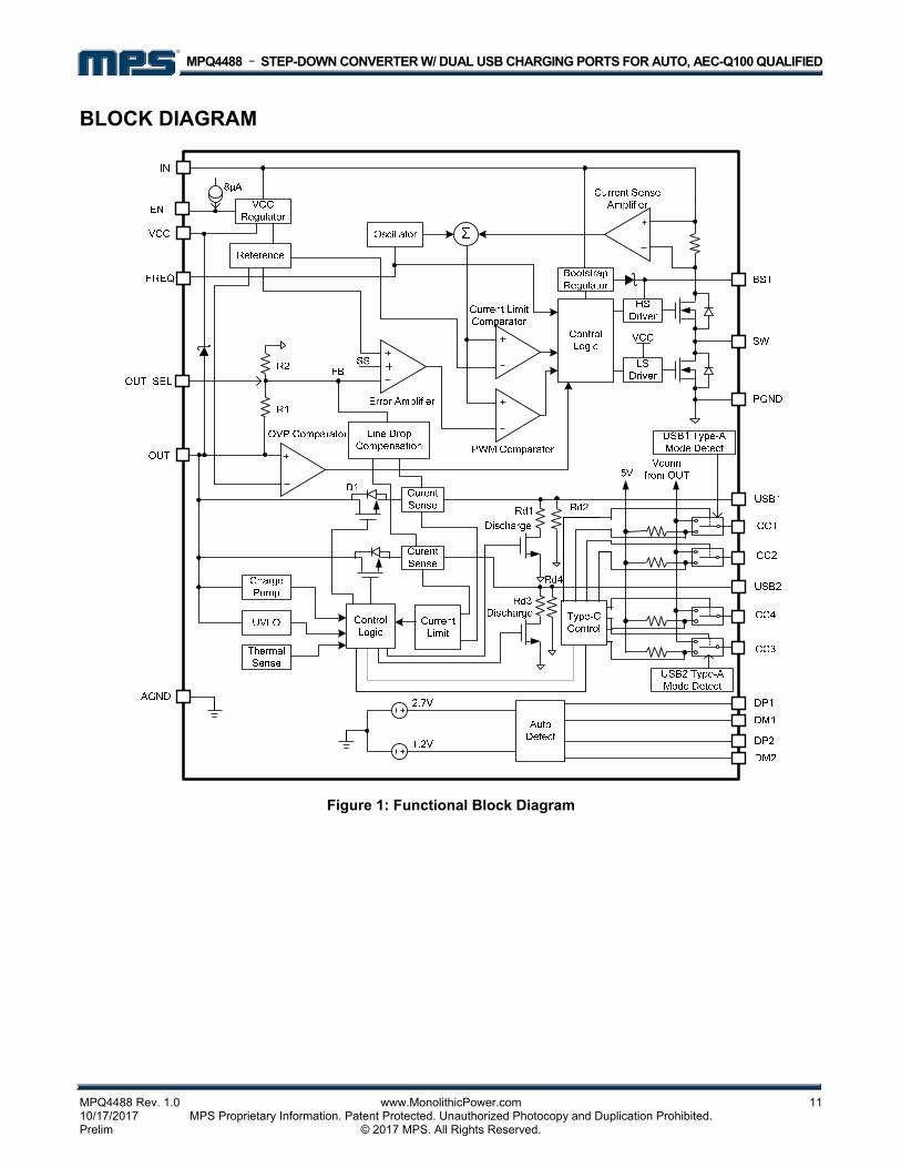
BLOCK DIAGRAM
Figure 1: Functional Block Diagram

MPQ4488 – STEP-DOWN CONVERTER W/ DUAL USB CHARGING PORTS FOR AUTO, AEC-Q100 QUALIFIED
MPQ4488 Rev. 1.0 www.MonolithicPower.com 12 10/17/2017 MPS Proprietary Information. Patent Protected. Unauthorized Photocopy and Duplication Prohibited. Prelim © 2017 MPS. All Rights Reserved.
OPERATION
BUCK CONVERTER SECTION The MPQ4488 integrates a monolithic, synchronous, rectified, step-down, switch-mode converter with internal power MOSFETs and two USB current-limit switches with charging port auto-detection. The MPQ4488 offers a compact solution that achieves 6A of continuous output current with excellent load and line regulation over a wide input supply range.
The MPQ4488 operates in a fixed-frequency, peak-current-mode control to regulate the output voltage. The internal clock initiates the pulse-width modulation (PWM) cycle, which turns on the integrated high-side power MOSFET (HS-FET). The HS-FET remains on until its current reaches the value set by the COMP voltage (VCOMP). When the power switch is off, it remains off until the next clock cycle begins. If the duty cycle reaches 95% (450kHz switching frequency) in one PWM period, the current in the power MOSFET does not reach the COMP-set current value, and the power MOSFET turns off.
Error Amplifier (EA)
The error amplifier (EA) compares the internal feedback voltage against the internal reference (REF) and outputs a VCOMP. This VCOMP controls the power MOSFET current. The optimized, internal compensation network minimizes the external component count and simplifies the control loop design.
Internal VCC Regulator
The 4.6V internal regulator powers most of the internal circuitries. This regulator takes VIN and operates in the full VIN range. When VIN exceeds 4.6V, the output of the regulator is in full regulation. If VIN is less than 4.6V, the output decreases with VIN. VCC requires an external 1µF ceramic decoupling capacitor.
After the buck output start-up, the internal VCC LDO output is biased by the buck output through a Schottky diode.
Enable Control (EN)
The MPQ4488 has an enable control pin (EN). There is an internal 8μA pull-up current that allows EN to be floated for automatic start-up.
Pulling EN high or floating EN enables the IC. Pulling EN low disables the IC. EN is clamped internally using a 7.6V series Zener diode and 10V breakdown voltage of an ESD cell (see Figure 2).
Connect EN through a pull-up resistor to VIN to enhance the EN pull-up current ability. This requires limiting the EN voltage below 10V or limiting the EN input current below 500μA if the EN pull-up voltage larger than 10V.
For example, connecting EN to VIN = 36V, RPULLUP ≥ (36V - 10V) / 500μA = 52kΩ.
Figure 2: Zener Diode between EN and GND
Setting the Switching Frequency
Connect a resistor from FREQ to ground to set the switching frequency (see Table 1). The value of the frequency can be calculated approximately with Equation (1):
ΩFREQ
1000000FREQ(kHz)
42.5 R (K ) 53.7 (1)
The frequency vs. RFREQ is shown in Figure 3.
Figure 3: Switching Frequency vs. RFREQ
200
700
1200
1700
2200
0 20 40 60 80 100 120

MPQ4488 – STEP-DOWN CONVERTER W/ DUAL USB CHARGING PORTS FOR AUTO, AEC-Q100 QUALIFIED
MPQ4488 Rev. 1.0 www.MonolithicPower.com 13 10/17/2017 MPS Proprietary Information. Patent Protected. Unauthorized Photocopy and Duplication Prohibited. Prelim © 2017 MPS. All Rights Reserved.
Table 1: Recommended Resistor Values for Typical Switching Frequency
RFREQ
(kΩ)
FS (kHz)
0 250
66.5 350
NC 450
45.8 500
22.3 1000
14.6 1500
9.53 2200
When running the part at a high switching frequency (i.e.: 2.2MHz), consider the minimum on time, minimum off time, and the maximum output current due to the thermal rise.
Two internal comparators monitor FREQ's logic voltage to enable FREQ to float or short to GND. During power-up, there is another internal source current on FREQ. The frequency is locked at 450kHz when a voltage greater than 2V is sensed on FREQ for longer than 8µs. The frequency is locked at 250kHz when a voltage less than 0.1V is sensed on FREQ for longer than 8µs. Leave FREQ floating or connect FREQ to VCC to achieve the 450kHz default switching frequency. Short FREQ to ground to achieve a 250kHz frequency (see Figure 4).
Figure 4: Switching Frequency Functional Block
Frequency Spread Spectrum
The purpose of the spread spectrum is to minimize the peak emissions at a specific frequency.
The MPQ4488GU-FD-AEC1 uses a 4kHz triangle wave (125μs rising, 125μs falling) to modulate the internal oscillator. The frequency span of the spread spectrum operation is ±10% (see Figure 5).
Figure 5: Frequency Spread Spectrum
FREQ must be floated or connected to VCC when using the spread spectrum function. The MPQ4488 can work without the switching frequency spread spectrum when FREQ is connected to an external resistor or shorted to GND.
Pull FREQ to GND to set the fixed switching frequency at 250kHz without the frequency spread spectrum. The frequency is determined by an external resistor when connecting FREQ to GND through a resistor.
Under-Voltage Lockout (UVLO)
Under-voltage lockout (UVLO) protects the chip from operating at an insufficient supply voltage. The UVLO comparator monitors the input voltage. The UVLO rising threshold is 5V, and its falling threshold is 4.3V.
Internal Soft Start (SS)
Soft start (SS) prevents the converter output voltage from overshooting during start-up. When the chip starts up, the internal circuitry generates a SS voltage that ramps up from 0V to 5V. When SS is lower than REF, the error amplifier uses SS as the reference. When SS is higher than REF, the error amplifier uses REF as the reference. The SS time is set to 2ms internally. If the output of the MPQ4488 is pre-biased to a certain voltage during start-up, the IC disables the switching of both the high-side and low-side switches until the voltage on the internal SS capacitor exceeds the internal feedback voltage.
Forced CCM Operation
The MPQ4488 works in forced continuous conduction mode (CCM) continuously. The MPQ4488 operates with a fixed switching frequency regardless of whether it is operating in light load or full load. The advantage of CCM is the controllable frequency, smaller output

MPQ4488 – STEP-DOWN CONVERTER W/ DUAL USB CHARGING PORTS FOR AUTO, AEC-Q100 QUALIFIED
MPQ4488 Rev. 1.0 www.MonolithicPower.com 14 10/17/2017 MPS Proprietary Information. Patent Protected. Unauthorized Photocopy and Duplication Prohibited. Prelim © 2017 MPS. All Rights Reserved.
ripple, and sufficient bootstrap charge time, but it also has low efficiency at light-load condition. A proper inductance should be selected to avoid triggering the low-side switch's negative current limit (typically 2A, from SW to GND). If the negative current limit is triggered, the low-side switch turns off, and the high-side switch turns on when the internal clock begins.
Buck Over-Current Protection (OCP)
The MPQ4488 has a cycle-by-cycle over-current limit when the inductor peak current exceeds the current-limit threshold, and the FB voltage drops below the under-voltage (UV) threshold (typically 50% below the reference). Once UV is triggered, the MPQ4488 enters hiccup mode to restart the part periodically. This protection mode is especially useful when the output is dead-shorted to ground. This reduces the average short-circuit current greatly, alleviates thermal issues, and protects the regulator. The MPQ4488 exits hiccup mode once the over-current condition is removed.
Buck Output Over-Voltage Protection (OVP)
The MPQ4488 has output over-voltage protection (OVP). If the output is higher than 5.85V, the high-side switch stops turning on. The low-side switch turns on to discharge the output voltage until the output decreases to 5.7V, and then the chip resumes normal operation.
Floating Driver and Bootstrap Charging
An external bootstrap capacitor powers the floating power MOSFET driver. This floating driver has its own UVLO protection. The UVLO’s rising threshold is 2.2V with a hysteresis of 150mV. The bootstrap capacitor voltage is regulated internally by VIN and VCC through D1, D2, M1, C4, L1, and C2 (see Figure 6). The BST capacitor (C4) voltage is charged up quickly by VCC through M1. The 2.5μA input to BST current source also can charge the BST capacitor when the low-side switch does not turn on.
Figure 6: Internal Bootstrap Charging Circuit
Start-Up and Shutdown
If both IN and EN exceed their respective thresholds, the chip is enabled. The reference block starts first, generating a stable reference voltage and current, and then the internal regulator is enabled. The regulator provides a stable supply for the remaining circuitries.
Three events can shut down the chip: EN low, IN low, and thermal shutdown. During shutdown, the signaling path is blocked to avoid any fault triggering. Then VCOMP and the internal supply rail are pulled down. The floating driver is not subject to this shutdown command.
Buck Output Impedance
The buck does not involve an output discharge function during EN shutdown. After EN shuts down, there are only two feedback resistors connected to OUT, which have a typical resistance of 160kΩ.
USB CURRENT-LIMIT SWITCH SECTION Over-Current Protection (OCP) and Hiccup
The MPQ4488 integrates two USB current-limit switches. The MPQ4488 provides built-in soft-start circuitry that controls the rising slew rate of the output voltage to limit inrush current and voltage surges.
When the load current reaches the current-limit threshold, the USB power MOSFET works in a constant current-limit mode (see Figure 7). If the over-current limit condition lasts longer than 5ms (VOUT does not drop too low), the corresponding USB channel enters hiccup mode with 5ms of on-time and 2s of off-time. Another USB channel still works normally.

MPQ4488 – STEP-DOWN CONVERTER W/ DUAL USB CHARGING PORTS FOR AUTO, AEC-Q100 QUALIFIED
MPQ4488 Rev. 1.0 www.MonolithicPower.com 15 10/17/2017 MPS Proprietary Information. Patent Protected. Unauthorized Photocopy and Duplication Prohibited. Prelim © 2017 MPS. All Rights Reserved.
Figure 7: Over-Current Limit
After the soft start finishes, if the USB output voltage is lower than 3.5V and lasts longer than 50µs, the MPQ4488 also enters hiccup (without having to wait for 5ms) (see Figure 8). This can prevent an abnormal thermal rise during a constant resistor (CR) load over-current case.
Figure 8: Over-Current Limit for CR Load
Fast Response for Short-Circuit Protection (SCP)
If the load current increases rapidly due to a short-circuit event, the current may exceed the current-limit threshold before the control loop is able to respond. If the current reaches the 7A secondary current limit level, a fast turn-off circuit is active to turn off the power MOSFET. This can help limit the peak current through the switch, keeping the buck output voltage from dropping too much and affect another USB channel. The total short-circuit response time is less than 1µs.
When the fast turn-off function is triggered, the MOSFET turns off for 100µs and restarts with a soft start. During the restart process, if the short still remains, the MPQ4488 regulates the gate voltage to hold the current at a normal current limit level.
Output Line Drop Compensation
The MPQ4488 can compensate for an output-voltage drop, such as high impedance caused
by a long trace, to maintain a fairly constant output voltage at the load-side voltage.
The internal comparator compares the current-sense output voltage of the two current-limit switches and uses the larger current-sense output voltage to compensate for the line drop voltage.
The line drop compensation amplitude increases linearly as the load current increases. It also has an upper limitation. The line drop compensation at output currents greater than 2.4A is 90mV.
USB Output Over-Voltage Clamp
To protect the device at the cable terminal, the USB switch output has a fixed over-voltage protection (OVP) threshold. When the input voltage is higher than the OVP threshold, the output voltage is clamped to its OVP threshold value.
USB Output Discharge and Impedance
Each USB switch has a fast discharge path that can discharge the external output capacitor's energy quickly during power shutdown. This function is active when the CC pins are released or the part is disabled (input voltage is under UVLO or EN off). The discharge path is turned off when the USB output voltage is discharged below 50mV. After the fast discharge path turns off, there is only a high impedance resistor (typically 500kΩ) from USB1 or USB2 to ground.
Auto-Detection
The MPQ4488 integrates a USB-dedicated charging port auto-detect function. This function recognizes most mainstream portable devices and supports the following charging schemes:
USB Battery Charging Specification BC1.2/ Chinese Telecommunications Industry Standard YD/T 1591-2009
Apple divider mode
1.2V/1.2V mode
USB Type-C 5V @ 3A DFP mode
The auto-detect function is a state machine that supports all of the DCP charging schemes above. Connect DP and DM with a 150Ω resistor for DCP mode.

MPQ4488 – STEP-DOWN CONVERTER W/ DUAL USB CHARGING PORTS FOR AUTO, AEC-Q100 QUALIFIED
MPQ4488 Rev. 1.0 www.MonolithicPower.com 16 10/17/2017 MPS Proprietary Information. Patent Protected. Unauthorized Photocopy and Duplication Prohibited. Prelim © 2017 MPS. All Rights Reserved.
USB Type-C Mode and VCONN
For USB Type-C solutions, two pins (CC1, CC2) on the connector are used to establish and manage the source-to-sink connection. The general concept for setting up a valid connection between a source and a sink is based on being able to detect terminations residing in the product being attached. To aid in defining the functional behavior of CC, a pull-up (Rp) and pull-down (Rd 5.1kΩ) termination model is used based on a pull-up resistor and pull-down resistor (see Figure 9).
Figure 9: Current Source/Pull-Down CC Model
Initially, a source exposes independent Rp terminations on its CC1 and CC2 pins, and a sink exposes independent Rd terminations on its CC1 and CC2 pins. The source-to-sink combination of this circuit configuration represents a valid connection. To detect this, the source monitors CC1 and CC2 for a voltage lower than its unterminated voltage. The choice of Rp is a function of the pull-up termination voltage and the source’s detection circuit. This indicates that either a sink, a powered cable, or a sink connected via a powered cable has been attached.
Prior to the application of VCONN, a powered cable exposes Ra (typically 1kΩ) on its VCONN pin. Ra represents the load on VCONN plus any resistive elements to ground. In some cable plugs, this might be a pure resistance, and in others, it may simply be the load.
The source must be able to differentiate between the presence of Rd and Ra to know whether there is a sink attached and where to apply VCONN. The source is not required to source VCONN unless Ra is detected.
Two special termination combinations on the CC pins as seen by a source are defined for directly attached accessory modes: Ra/Ra for audio adapter accessory mode and Rd/Rd for
debug accessory mode (see Figure 10 and Table 2).
Figure 10: CC Pin Functional Block
A port that behaves as a source has the following functional characteristics.
1. The source uses a MOSFET to enable or disable the power delivery across VBUS. Initially, the source is disabled.
2. The source supplies pull-up resistors (Rp) on CC1 and CC2 and monitors both to detect a sink. The presence of an Rd pull-down resistor on either CC1 or CC2 indicates that a sink is being attached. The value of Rp indicates the initial USB Type-C current level supported by the host. The MPQ4488 default Rp is 10kΩ, which represents a 3A current level.
3. The source uses the CC pull-down characteristic to detect and determine which CC pin is intended to supply VCONN (when Ra is discovered).
4. Once a sink is detected, the source enables VBUS and VCONN.
5. The source can adjust the value of Rp dynamically to indicate a change in the available USB Type-C current to a sink. For example, at high temperature, the MPQ4488 changes Rp to 22kΩ to indicate a 1.5A current ability.
6. The source monitors the continued presence of Rd to detect a sink detach. When a detach event is detected, the source is removed, VBUS and VCONN return to step 2.
MPQ4488 – STEP-DOWN CONVERTER W/ DUAL USB CHARGING PORTS FOR AUTO, AEC-Q100 QUALIFIED
MPQ4488 Rev. 1.0 www.MonolithicPower.com 17 10/17/2017 MPS Proprietary Information. Patent Protected. Unauthorized Photocopy and Duplication Prohibited. Prelim © 2017 MPS. All Rights Reserved.
Disable Type-C Mode (Type-A Mode)
During the MPQ4488 initial start-up, the IC sources 10μA for 20μs on CC1. If the CC1 voltage falls into a 400mV to 1.2V range, USB1 latches in Type-A mode unless the part is re-enabled. Type-C mode is disabled, so CC1's attach and detach logic is disabled, and VBUS is always enabled. The current limit changes to a Type-A spec. The same logic is implemented on CC3 for USB2.
To trigger Type-A mode, the external pull-down resistor should be 70 - 90kΩ. Do not connect extra capacitors on CC1 and CC3.
In normal Type-C mode applications, a 1nF capacitor should be added on CC1 and CC3 to avoid falsely triggering Type-A mode. If two Ra resistors pull down CC1 and CC2, or two Rd resistors pull down CC1 and CC2, there is no action inside the IC (VBUS is not enabled).
Load Shedding vs. Temperature
The MPQ4488 monitors the die temperature and changes its output current capability dynamically. This feature is supported by both Type-C and USB2.0 applications.
If the die temperature is higher than 125°C, the USB port's CC pin pull-up resistance (Rp) changes to 22kΩ to indicate that its source capability has changed to 1.5A. Meanwhile, VBUS changes to 4.77V.
If the die temperature is lower than 100°C for 16 seconds, VBUS reverts back to the normal voltage set by OUT_SEL. Meanwhile, the USB Type-C current capability changes back to 3A (Rp = 10kΩ). The current limit threshold remains at 3.55A during this period.
Thermal Shutdown
Thermal shutdown prevents the chip from operating at exceedingly high temperatures. When the silicon die temperature exceeds 165°C, the entire chip shuts down. When the temperature falls below its lower threshold (typically 145°C), the chip is enabled.

MPQ4488 – STEP-DOWN CONVERTER W/ DUAL USB CHARGING PORTS FOR AUTO, AEC-Q100 QUALIFIED
MPQ4488 Rev. 1.0 www.MonolithicPower.com 18 10/17/2017 MPS Proprietary Information. Patent Protected. Unauthorized Photocopy and Duplication Prohibited. Prelim © 2017 MPS. All Rights Reserved.
Table 2: CC Logic Truth Table
EN CC of USB1 (8) CC of USB2 (8) Buck VCONN(USB1)
USB1 VCONN (USB2)
USB2
0 X X Disabled Disabled Disabled Disabled Disabled
1
AUDIO
Open or AUDIO or DEBUG
Disabled Disabled Disabled Disabled Disabled DEBUG Disabled Disabled Disabled Disabled Disabled
“A” (9) Enabled Disabled Enabled Disabled Disabled Rd, Ra Enabled Enabled Enabled Disabled Disabled Open Disabled Disabled Disabled Disabled Disabled
1
AUDIO
Rd, Ra
Enabled Disabled Disabled Enabled Enabled DEBUG Enabled Disabled Disabled Enabled Enabled
“A” Enabled Disabled Enabled Enabled Enabled Rd, Ra Enabled Enabled Enabled Enabled Enabled Open Enabled Disabled Disabled Enabled Enabled
1
AUDIO
“A”
Enabled Disabled Disabled Disabled Enabled DEBUG Enabled Disabled Disabled Disabled Enabled
“A” Enabled Disabled Enabled Disabled Enabled Rd, Ra Enabled Enabled Enabled Disabled Enabled Open Enabled Disabled Disabled Disabled Enabled
NOTES: 8) USB1 and USB2 are symmetrical to each other. 9) "A" means Type-A mode. CC1 (CC3 for USB2) is requested to be pulled down by a 80.6kΩ resistor to enter this mode.

MPQ4488 – STEP-DOWN CONVERTER W/ DUAL USB CHARGING PORTS FOR AUTO, AEC-Q100 QUALIFIED
MPQ4488 Rev. 1.0 www.MonolithicPower.com 19 10/17/2017 MPS Proprietary Information. Patent Protected. Unauthorized Photocopy and Duplication Prohibited. Prelim © 2017 MPS. All Rights Reserved.
APPLICATION INFORMATION Selecting the Inductor
For most applications, use an inductor with a DC current rating at least 25% higher than the maximum load current. Select an inductor with a small DC resistance for optimum efficiency. For most designs the inductor value can be derived with Equation (2):
OUT IN OUT1
IN L OSC
V (V V )L
V I f
(2)
Where ∆IL is the inductor ripple current.
Choose the inductor ripple current to be approximately 30% of the maximum load current. The maximum inductor peak current can be calculated with Equation (3):
2
III LLOAD)MAX(L
(3)
Selecting Buck Input Capacitor
The input current to the step-down converter is discontinuous and therefore requires a capacitor to supply AC current while maintaining the DC input voltage. Use low ESR capacitors for optimum performance. Ceramic capacitors with X5R or X7R dielectrics are highly recommended because of their low ESR and small temperature coefficients. 100µF electrolytic and 50µF ceramic capacitors are recommended in automotive applications at a 450kHz switching frequency.
Since the input capacitor (C1) absorbs the input switching current, it requires an adequate ripple current rating. The RMS current in the input capacitor can be estimated with Equation (4):
IN
OUT
IN
OUTLOAD1C V
V1V
VII (4)
The worst-case condition occurs at VIN = 2VOUT, shown in Equation (5):
2
II LOAD
1C (5)
For simplification, choose an input capacitor with an RMS current rating greater than half of the maximum load current.
The input capacitor can be electrolytic, tantalum, or ceramic. When using an electrolytic capacitor, place two additional high-quality ceramic capacitors as close to IN as possible. Estimate the input voltage ripple caused by the capacitance with Equation (6):
LOAD OUT OUTIN
INS IN
I V VV 1
f C1 V V
(6)
Selecting Buck Output Capacitor
The device requires an output capacitor (C2) to maintain the DC output voltage. Estimate the output voltage ripple with Equation (7):
OUT OUTOUT ESR
S 1 IN S
V V 1V 1 R
f L V 8 f C2
(7)
Where L1 is the inductor value, and RESR is the equivalent series resistance (ESR) value of the output capacitor.
For an electrolytic capacitor, the ESR dominates the impedance at the switching frequency. For simplification, the output ripple can be approximated with Equation (8):
OUT OUTOUT ESR
INS 1
V V∆V 1 R
f L V
(8)
A 100 - 270μF capacitor with an ESR less than 50mΩ (e.g.: polymer or tantalum capacitors) and three 10μF ceramic capacitors are recommended in applications (see Table 3).
Table 3: Recommended External Components
Switching Frequency
InductorInput
capacitor Buck Output
Capacitor
250kHz 8μH
50µF ceramic cap +
100µF E-cap
30µF ceramic cap + 270µF Polymer cap
450kHz 4.7μH
50µF ceramic cap +
100µF E-cap
30µF ceramic cap + 270µF Polymer cap
MPQ4488 – STEP-DOWN CONVERTER W/ DUAL USB CHARGING PORTS FOR AUTO, AEC-Q100 QUALIFIED
MPQ4488 Rev. 1.0 www.MonolithicPower.com 20 10/17/2017 MPS Proprietary Information. Patent Protected. Unauthorized Photocopy and Duplication Prohibited. Prelim © 2017 MPS. All Rights Reserved.
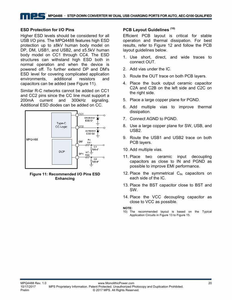
ESD Protection for I/O Pins
Higher ESD levels should be considered for all USB I/O pins. The MPQ4488 features high ESD protection up to ±8kV human body model on DP, DM, USB1, and USB2, and ±5.5kV human body model on CC1 through CC4. The ESD structures can withstand high ESD both in normal operation and when the device is powered off. To further extend DP and DM's ESD level for covering complicated application environments, additional resistors and capacitors can be added (see Figure 11).
Similar R-C networks cannot be added on CC1 and CC2 pins since the CC line must support a 200mA current and 300kHz signaling. Additional ESD diodes can be added on CC.
Figure 11: Recommended I/O Pins ESD Enhancing
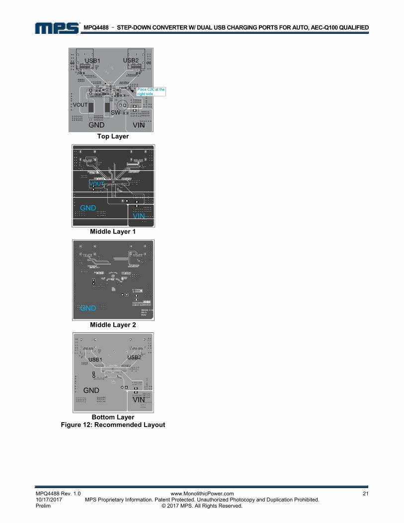
PCB Layout Guidelines (10)
Efficient PCB layout is critical for stable operation and thermal dissipation. For best results, refer to Figure 12 and follow the PCB layout guidelines below.
1. Use short, direct, and wide traces to connect OUT.
2. Add vias under the IC.
3. Route the OUT trace on both PCB layers.
4. Place the buck output ceramic capacitor C2A and C2B on the left side and C2C on the right side.
5. Place a large copper plane for PGND.
6. Add multiple vias to improve thermal dissipation.
7. Connect AGND to PGND.
8. Use a large copper plane for SW, USB, and USB2.
9. Route the USB1 and USB2 trace on both PCB layers.
10. Add multiple vias.
11. Place two ceramic input decoupling capacitors as close to IN and PGND as possible to improve EMI performance.
12. Place the symmetrical CIN capacitors on each side of the IC.
13. Place the BST capacitor close to BST and SW.
14. Place the VCC decoupling capacitor as close to VCC as possible.
NOTE: 10) The recommended layout is based on the Typical
Application Circuits in Figure 13 to Figure 15.
MPQ4488 – STEP-DOWN CONVERTER W/ DUAL USB CHARGING PORTS FOR AUTO, AEC-Q100 QUALIFIED
MPQ4488 Rev. 1.0 www.MonolithicPower.com 21 10/17/2017 MPS Proprietary Information. Patent Protected. Unauthorized Photocopy and Duplication Prohibited. Prelim © 2017 MPS. All Rights Reserved.
Top Layer
Middle Layer 1
Middle Layer 2
Bottom Layer
Figure 12: Recommended Layout
VIN GND
USB1 USB2
VOUT
SW
VIN GND
VOUT
GND
VIN GND
USB1 USB2
MPQ4488 – STEP-DOWN CONVERTER W/ DUAL USB CHARGING PORTS FOR AUTO, AEC-Q100 QUALIFIED
MPQ4488 Rev. 1.0 www.MonolithicPower.com 22 10/17/2017 MPS Proprietary Information. Patent Protected. Unauthorized Photocopy and Duplication Prohibited. Prelim © 2017 MPS. All Rights Reserved.
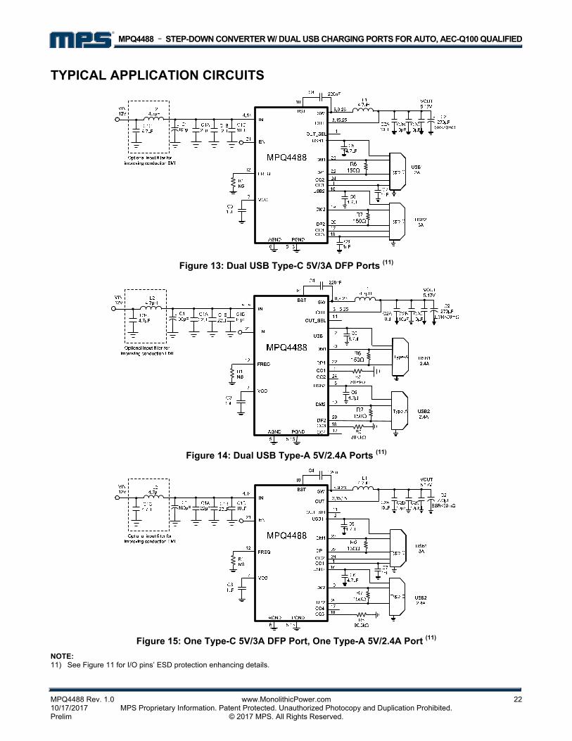
TYPICAL APPLICATION CIRCUITS
Figure 13: Dual USB Type-C 5V/3A DFP Ports (11)
Figure 14: Dual USB Type-A 5V/2.4A Ports (11)
Figure 15: One Type-C 5V/3A DFP Port, One Type-A 5V/2.4A Port (11)
NOTE: 11) See Figure 11 for I/O pins’ ESD protection enhancing details.
MPQ4488 – STEP-DOWN CONVERTER W/ DUAL USB CHARGING PORTS FOR AUTO, AEC-Q100 QUALIFIED
NOTICE: The information in this document is subject to change without notice. Users should warrant and guarantee that third party Intellectual Property rights are not infringed upon when integrating MPS products into any application. MPS will not assume any legal responsibility for any said applications.
MPQ4488 Rev1.0 www.MonolithicPower.com 2323 10/17/2017 MPS Proprietary Information. Patent Protected. Unauthorized Photocopy and Duplication Prohibited. © 2017 MPS. All Rights Reserved.
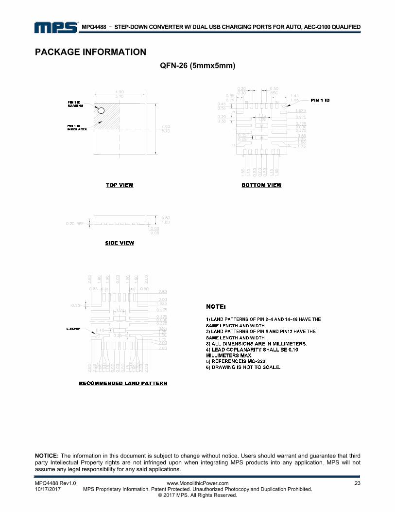
PACKAGE INFORMATION
QFN-26 (5mmx5mm)