mpu-6500 register map and descriptions revision 2 · mpu-6500 register map and descriptions...
TRANSCRIPT

InvenSense Inc. 1197 Borregas Ave, Sunnyvale, CA 94089 U.S.A. Tel: +1 (408) 988-7339 Fax: +1 (408) 988-8104
Website: www.invensense.com
Document Number: RM-MPU-6500A-00 Revision: 2.1 Release Date: 09/16/2013
MPU-6500 Register Map and Descriptions
Revision 2.1
1 of 47
MPU-6500 Register Map and Descriptions
Document Number: RM-MPU-6500A-00 Revision: 2.1 Release Date: 09/16/2013
CONTENTS 1 REVISION HISTORY ................................................................................................................................... 4
2 PURPOSE AND SCOPE ............................................................................................................................. 5
3 REGISTER MAP .......................................................................................................................................... 6
4 REGISTER DESCRIPTIONS ..................................................................................................................... 10
4.1 REGISTERS 0 TO 2 – GYROSCOPE SELF-TEST REGISTERS .................................................................. 10
4.2 REGISTERS 13 TO 15 – ACCELEROMETER SELF-TEST REGISTERS ....................................................... 10 4.3 REGISTERS 19 TO 24 – GYRO OFFSET REGISTERS ............................................................................. 11
4.4 REGISTER 25 – SAMPLE RATE DIVIDER .............................................................................................. 12
4.5 REGISTER 26 – CONFIGURATION ........................................................................................................ 13
4.6 REGISTER 27 – GYROSCOPE CONFIGURATION .................................................................................... 14
4.7 REGISTER 28 – ACCELEROMETER CONFIGURATION ............................................................................. 14
4.8 REGISTER 29 – ACCELEROMETER CONFIGURATION 2 .......................................................................... 15 4.9 REGISTER 30 – LOW POWER ACCELEROMETER ODR CONTROL .......................................................... 17
4.10 REGISTER 31 – WAKE-ON MOTION THRESHOLD .................................................................................. 17
4.11 REGISTER 35 – FIFO ENABLE ............................................................................................................ 18
4.12 REGISTER 36 – I2C MASTER CONTROL .............................................................................................. 19
4.13 REGISTERS 37 TO 39 – I2C SLAVE 0 CONTROL ................................................................................... 20
REGISTER 37 - I2C_SLV0_ADDR .................................................................................................................. 20 REGISTER 38 - I2C_SLV0_REG .................................................................................................................... 20
REGISTER 39 - I2C_SLV0_CTRL ................................................................................................................... 20
4.14 REGISTERS 40 TO 42 – I2C SLAVE 1 CONTROL ................................................................................... 21
REGISTER 40 - I2C_SLV1_ADDR .................................................................................................................. 21
REGISTER 41 - I2C_SLV1_REG .................................................................................................................... 22 REGISTER 42 - I2C_SLV1_CTRL ................................................................................................................... 22
4.15 REGISTERS 43 TO 45 – I2C SLAVE 2 CONTROL ................................................................................... 23
REGISTER 43 - I2C_SLV2_ADDR .................................................................................................................. 23
REGISTER 44 - I2C_SLV2_REG .................................................................................................................... 24
REGISTER 45 - I2C_SLV2_CTRL ................................................................................................................... 24
4.16 REGISTERS 46 TO 48 – I2C SLAVE 3 CONTROL ................................................................................... 25 REGISTER 46 - I2C_SLV3_ADDR .................................................................................................................. 25
REGISTER 47 - I2C_SLV3_REG .................................................................................................................... 25
REGISTER 48 - I2C_SLV3_CTRL ................................................................................................................... 25
4.17 REGISTERS 49 TO 53 – I2C SLAVE 4 CONTROL ................................................................................... 26
2 of 47
MPU-6500 Register Map and Descriptions
Document Number: RM-MPU-6500A-00 Revision: 2.1 Release Date: 09/16/2013
REGISTER 49 - I2C_SLV4_ADDR .................................................................................................................. 26
REGISTER 50 - I2C_SLV4_REG .................................................................................................................... 26
REGISTER 51 - I2C_SLV4_DO ....................................................................................................................... 27
REGISTER 52 - I2C_SLV4_CTRL ................................................................................................................... 27
REGISTER 53 - I2C_SLV4_DI ......................................................................................................................... 27 4.18 REGISTER 54 – I2C MASTER STATUS .................................................................................................. 28
4.19 REGISTER 55 – INT PIN / BYPASS ENABLE CONFIGURATION ................................................................ 29
4.20 REGISTER 56 – INTERRUPT ENABLE ................................................................................................... 29
4.21 REGISTER 58 – INTERRUPT STATUS ................................................................................................... 30
4.22 REGISTERS 59 TO 64 – ACCELEROMETER MEASUREMENTS ................................................................. 31
4.23 REGISTERS 65 AND 66 – TEMPERATURE MEASUREMENT ..................................................................... 33 4.24 REGISTERS 67 TO 72 – GYROSCOPE MEASUREMENTS ........................................................................ 33
4.25 REGISTERS 73 TO 96 – EXTERNAL SENSOR DATA ............................................................................... 35
4.26 REGISTER 99 – I2C SLAVE 0 DATA OUT .............................................................................................. 37
4.27 REGISTER 100 – I2C SLAVE 1 DATA OUT ............................................................................................ 37
4.28 REGISTER 101 – I2C SLAVE 2 DATA OUT ............................................................................................ 37
4.29 REGISTER 102 – I2C SLAVE 3 DATA OUT ............................................................................................ 38 4.30 REGISTER 103 – I2C MASTER DELAY CONTROL .................................................................................. 38
4.31 REGISTER 104 – SIGNAL PATH RESET ................................................................................................ 39
4.32 REGISTER 105 – ACCELEROMETER INTERRUPT CONTROL ................................................................... 39
4.33 REGISTER 106 – USER CONTROL ....................................................................................................... 40
4.34 REGISTER 107 – POWER MANAGEMENT 1 .......................................................................................... 41 4.35 REGISTER 108 – POWER MANAGEMENT 2 .......................................................................................... 42
4.36 REGISTER 114 AND 115 – FIFO COUNT REGISTERS ........................................................................... 43
4.37 REGISTER 116 – FIFO READ WRITE .................................................................................................. 43
4.38 REGISTER 117 – WHO AM I ................................................................................................................ 44
4.39 REGISTERS 119, 120, 122, 123, 125, 126 ACCELEROMETER OFFSET REGISTERS ............................... 44
3 of 47
MPU-6500 Register Map and Descriptions
Document Number: RM-MPU-6500A-00 Revision: 2.1 Release Date: 09/16/2013
1 Revision History
Revision Date Revision Description 06/29/2012 1.0 Initial Release
07/15/2013 2.0 Updated Release
09/16/2013 2.1 Updated sections 3 and 4
4 of 47

MPU-6500 Register Map and Descriptions
Document Number: RM-MPU-6500A-00 Revision: 2.1 Release Date: 09/16/2013
2 Purpose and Scope This document provides preliminary information regarding the register map and descriptions for the Motion Processing Unit™ MPU-6500™. This document should be used in conjunction with the MPU-6500 Product Specification (PS-MPU-6500A-00) for detailed features, specifications, and other product information.
5 of 47
MPU-6500 Register Map and Descriptions
Document Number: RM-MPU-6500A-00 Revision: 2.1 Release Date: 09/16/2013
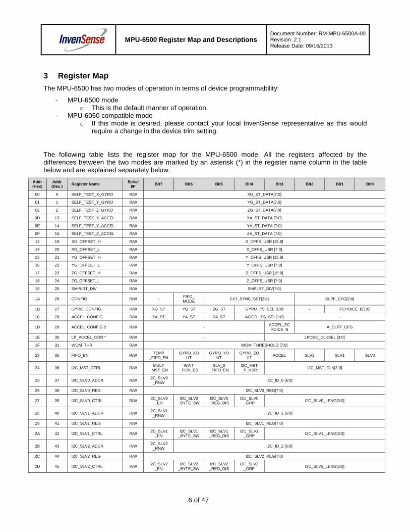
3 Register Map The MPU-6500 has two modes of operation in terms of device programmability:
- MPU-6500 mode o This is the default manner of operation.
- MPU-6050 compatible mode o If this mode is desired, please contact your local InvenSense representative as this would
require a change in the device trim setting.
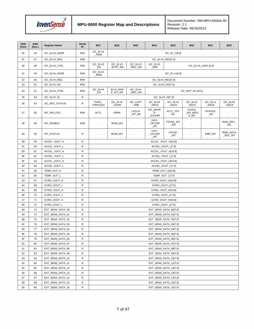
The following table lists the register map for the MPU-6500 mode. All the registers affected by the differences between the two modes are marked by an asterisk (*) in the register name column in the table below and are explained separately below.
Addr (Hex)
Addr (Dec.) Register Name Serial
I/F Bit7 Bit6 Bit5 Bit4 Bit3 Bit2 Bit1 Bit0
00 0 SELF_TEST_X_GYRO R/W XG_ST_DATA[7:0]
01 1 SELF_TEST_Y_GYRO R/W YG_ST_DATA[7:0]
02 2 SELF_TEST_Z_GYRO R/W ZG_ST_DATA[7:0]
0D 13 SELF_TEST_X_ACCEL R/W XA_ST_DATA [7:0]
0E 14 SELF_TEST_Y_ACCEL R/W YA_ST_DATA [7:0]
0F 15 SELF_TEST_Z_ACCEL R/W ZA_ST_DATA [7:0]
13 19 XG_OFFSET_H R/W X_OFFS_USR [15:8]
14 20 XG_OFFSET_L R/W X_OFFS_USR [7:0]
15 21 YG_OFFSET_H R/W Y_OFFS_USR [15:8]
16 22 YG_OFFSET_L R/W Y_OFFS_USR [7:0]
17 23 ZG_OFFSET_H R/W Z_OFFS_USR [15:8]
18 24 ZG_OFFSET_L R/W Z_OFFS_USR [7:0]
19 25 SMPLRT_DIV R/W SMPLRT_DIV[7:0]
1A 26 CONFIG R/W - FIFO_ MODE EXT_SYNC_SET[2:0] DLPF_CFG[2:0]
1B 27 GYRO_CONFIG R/W XG_ST YG_ST ZG_ST GYRO_FS_SEL [1:0] - FCHOICE_B[1:0]
1C 28 ACCEL_CONFIG R/W XA_ST YA_ST ZA_ST ACCEL_FS_SEL[1:0] -
1D 29 ACCEL_CONFIG 2 R/W - ACCEL_FCHOICE_B A_DLPF_CFG
1E 30 LP_ACCEL_ODR * R/W - LPOSC_CLKSEL [3:0]
1F 31 WOM_THR R/W WOM_THRESHOLD [7:0]
23 35 FIFO_EN R/W TEMP _FIFO_EN
GYRO_XOUT
GYRO_YOUT
GYRO_ZOUT ACCEL SLV2 SLV1 SLV0
24 36 I2C_MST_CTRL R/W MULT _MST_EN
WAIT _FOR_ES
SLV_3 _FIFO_EN
I2C_MST _P_NSR I2C_MST_CLK[3:0]
25 37 I2C_SLV0_ADDR R/W I2C_SLV0 _RNW I2C_ID_0 [6:0]
26 38 I2C_SLV0_REG R/W I2C_SLV0_REG[7:0]
27 39 I2C_SLV0_CTRL R/W I2C_SLV0 _EN
I2C_SLV0 _BYTE_SW
I2C_SLV0 _REG_DIS
I2C_SLV0 _GRP I2C_SLV0_LENG[3:0]
28 40 I2C_SLV1_ADDR R/W I2C_SLV1 _RNW I2C_ID_1 [6:0]
29 41 I2C_SLV1_REG R/W I2C_SLV1_REG[7:0]
2A 42 I2C_SLV1_CTRL R/W I2C_SLV1 _EN
I2C_SLV1 _BYTE_SW
I2C_SLV1 _REG_DIS
I2C_SLV1 _GRP I2C_SLV1_LENG[3:0]
2B 43 I2C_SLV2_ADDR R/W I2C_SLV2 _RNW I2C_ID_2 [6:0]
2C 44 I2C_SLV2_REG R/W I2C_SLV2_REG[7:0]
2D 45 I2C_SLV2_CTRL R/W I2C_SLV2 _EN
I2C_SLV2 _BYTE_SW
I2C_SLV2 _REG_DIS
I2C_SLV2 _GRP I2C_SLV2_LENG[3:0]
6 of 47
MPU-6500 Register Map and Descriptions
Document Number: RM-MPU-6500A-00 Revision: 2.1 Release Date: 09/16/2013
Addr (Hex)
Addr (Dec.) Register Name Serial
I/F Bit7 Bit6 Bit5 Bit4 Bit3 Bit2 Bit1 Bit0
2E 46 I2C_SLV3_ADDR R/W I2C_SLV3 _RNW I2C_ID_3 [6:0]
2F 47 I2C_SLV3_REG R/W I2C_SLV3_REG[7:0]
30 48 I2C_SLV3_CTRL R/W I2C_SLV3 _EN
I2C_SLV3 _BYTE_SW
I2C_SLV3 _REG_DIS
I2C_SLV3 _GRP I2C_SLV3_LENG [3:0]
31 49 I2C_SLV4_ADDR R/W I2C_SLV4 _RNW I2C_ID_4 [6:0]
32 50 I2C_SLV4_REG R/W I2C_SLV4_REG[7:0]
33 51 I2C_SLV4_DO R/W I2C_SLV4_DO[7:0]
34 52 I2C_SLV4_CTRL R/W I2C_SLV4 _EN
SLV4_DONE_INT_EN
I2C_SLV4 _REG_DIS I2C_MST_DLY[4:0]
35 53 I2C_SLV4_DI R I2C_SLV4_DI[7:0]
36 54 I2C_MST_STATUS R PASS_ THROUGH
I2C_SLV4 _DONE
I2C_LOST _ARB
I2C_SLV4 _NACK
I2C_SLV3 _NACK
I2C_SLV2 _NACK
I2C_SLV1 _NACK
I2C_SLV0 _NACK
37 55 INT_PIN_CFG R/W ACTL OPEN LATCH _INT_EN
INT_ANYRD
_2CLEAR
ACTL_FSYNC
FSYNC _INT_MOD
E_EN
BYPASS _EN -
38 56 INT_ENABLE R/W - WOM_EN - FIFO
_OFLOW _EN
FSYNC_INT_EN - - RAW_RDY_
EN
3A 58 INT_STATUS R - WOM_INT - FIFO
_OFLOW _INT
FSYNC _INT - DMP_INT RAW_DATA
_RDY_INT
3B 59 ACCEL_XOUT_H R ACCEL_XOUT_H[15:8]
3C 60 ACCEL_XOUT_L R ACCEL_XOUT_L[7:0]
3D 61 ACCEL_YOUT_H R ACCEL_YOUT_H[15:8]
3E 62 ACCEL_YOUT_L R ACCEL_YOUT_L[7:0]
3F 63 ACCEL_ZOUT_H R ACCEL_ZOUT_H[15:8]
40 64 ACCEL_ZOUT_L R ACCEL_ZOUT_L[7:0]
41 65 TEMP_OUT_H R TEMP_OUT_H[15:8]
42 66 TEMP_OUT_L R TEMP_OUT_L[7:0]
43 67 GYRO_XOUT_H R GYRO_XOUT_H[15:8]
44 68 GYRO_XOUT_L R GYRO_XOUT_L[7:0]
45 69 GYRO_YOUT_H R GYRO_YOUT_H[15:8]
46 70 GYRO_YOUT_L R GYRO_YOUT_L[7:0]
47 71 GYRO_ZOUT_H R GYRO_ZOUT_H[15:8]
48 72 GYRO_ZOUT_L R GYRO_ZOUT_L[7:0]
49 73 EXT_SENS_DATA_00 R EXT_SENS_DATA_00[7:0]
4A 74 EXT_SENS_DATA_01 R EXT_SENS_DATA_01[7:0]
4B 75 EXT_SENS_DATA_02 R EXT_SENS_DATA_02[7:0]
4C 76 EXT_SENS_DATA_03 R EXT_SENS_DATA_03[7:0]
4D 77 EXT_SENS_DATA_04 R EXT_SENS_DATA_04[7:0]
4E 78 EXT_SENS_DATA_05 R EXT_SENS_DATA_05[7:0]
4F 79 EXT_SENS_DATA_06 R EXT_SENS_DATA_06[7:0]
50 80 EXT_SENS_DATA_07 R EXT_SENS_DATA_07[7:0]
51 81 EXT_SENS_DATA_08 R EXT_SENS_DATA_08[7:0]
52 82 EXT_SENS_DATA_09 R EXT_SENS_DATA_09[7:0]
53 83 EXT_SENS_DATA_10 R EXT_SENS_DATA_10[7:0]
54 84 EXT_SENS_DATA_11 R EXT_SENS_DATA_11[7:0]
55 85 EXT_SENS_DATA_12 R EXT_SENS_DATA_12[7:0]
56 86 EXT_SENS_DATA_13 R EXT_SENS_DATA_13[7:0]
57 87 EXT_SENS_DATA_14 R EXT_SENS_DATA_14[7:0]
58 88 EXT_SENS_DATA_15 R EXT_SENS_DATA_15[7:0]
59 89 EXT_SENS_DATA_16 R EXT_SENS_DATA_16[7:0]
7 of 47
MPU-6500 Register Map and Descriptions
Document Number: RM-MPU-6500A-00 Revision: 2.1 Release Date: 09/16/2013
Addr (Hex)
Addr (Dec.) Register Name Serial
I/F Bit7 Bit6 Bit5 Bit4 Bit3 Bit2 Bit1 Bit0
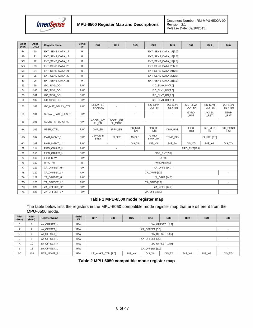
5A 90 EXT_SENS_DATA_17 R EXT_SENS_DATA_17[7:0]
5B 91 EXT_SENS_DATA_18 R EXT_SENS_DATA_18[7:0]
5C 92 EXT_SENS_DATA_19 R EXT_SENS_DATA_19[7:0]
5D 93 EXT_SENS_DATA_20 R EXT_SENS_DATA_20[7:0]
5E 94 EXT_SENS_DATA_21 R EXT_SENS_DATA_21[7:0]
5F 95 EXT_SENS_DATA_22 R EXT_SENS_DATA_22[7:0]
60 96 EXT_SENS_DATA_23 R EXT_SENS_DATA_23[7:0]
63 99 I2C_SLV0_DO R/W I2C_SLV0_DO[7:0]
64 100 I2C_SLV1_DO R/W I2C_SLV1_DO[7:0]
65 101 I2C_SLV2_DO R/W I2C_SLV2_DO[7:0]
66 102 I2C_SLV3_DO R/W I2C_SLV3_DO[7:0]
67 103 I2C_MST_DELAY_CTRL R/W DELAY_ES _SHADOW - - I2C_SLV4
_DLY_EN I2C_SLV3 _DLY_EN
I2C_SLV2 _DLY_EN
I2C_SLV1 _DLY_EN
I2C_SLV0 _DLY_EN
68 104 SIGNAL_PATH_RESET R/W - - - - - GYRO _RST
ACCEL _RST
TEMP _RST
69 105 ACCEL_INTEL_CTRL R/W ACCEL_INTEL_EN
ACCEL_INTEL_MODE - - -
6A 106 USER_CTRL R/W DMP_EN FIFO_EN I2C_MST _EN
I2C_IF _DIS DMP_RST FIFO
_RST I2C_MST
_RST SIG_COND
_RST
6B 107 PWR_MGMT_1 R/W DEVICE_RESET SLEEP CYCLE GYRO_
STANDBY TEMP_DIS CLKSEL[2:0]
6C 108 PWR_MGMT_2 * R/W - DIS_XA DIS_YA DIS_ZA DIS_XG DIS_YG DIS_ZG
72 114 FIFO_COUNT_H R/W - FIFO_CNT[12:8]
73 115 FIFO_COUNT_L R/W FIFO_CNT[7:0]
74 116 FIFO_R_W R/W D[7:0]
75 117 WHO_AM_I R WHOAMI[7:0]
77 119 XA_OFFSET_H * R/W XA_OFFS [14:7]
78 120 XA_OFFSET_L * R/W XA_OFFS [6:0] -
7A 122 YA_OFFSET_H * R/W YA_OFFS [14:7]
7B 123 YA_OFFSET_L * R/W YA_OFFS [6:0] -
7D 125 ZA_OFFSET_H * R/W ZA_OFFS [14:7]
7E 126 ZA_OFFSET_L * R/W ZA_OFFS [6:0] -
Table 1 MPU-6500 mode register map
The table below lists the registers in the MPU-6050 compatible mode register map that are different from the MPU-6500 mode.
Addr (Hex)
Addr (Dec.) Register Name Serial
I/F Bit7 Bit6 Bit5 Bit4 Bit3 Bit2 Bit1 Bit0
6 6 XA_OFFSET_H R/W XA_OFFSET [14:7]
7 7 XA_OFFSET_L R/W XA_OFFSET [6:0] -
8 8 YA_OFFSET_H R/W YA_OFFSET [14:7]
9 9 YA_OFFSET_L R/W YA_OFFSET [6:0] -
A 10 ZA_OFFSET_H R/W ZA_OFFSET [14:7]
B 11 ZA_OFFSET_L R/W ZA_OFFSET [6:0] -
6C 108 PWR_MGMT_2 R/W LP_WAKE_CTRL[1:0] DIS_XA DIS_YA DIS_ZA DIS_XG DIS_YG DIS_ZG
Table 2 MPU-6050 compatible mode register map
8 of 47
MPU-6500 Register Map and Descriptions
Document Number: RM-MPU-6500A-00 Revision: 2.1 Release Date: 09/16/2013
Note: Register Names ending in _H and _L contain the high and low bytes, respectively, of an internal register value. In the detailed register tables that follow, register names are in capital letters, while register values are in capital letters and italicized. For example, the ACCEL_XOUT_H register (Register 59) contains the 8 most significant bits, ACCEL_XOUT[15:8], of the 16-bit X-Axis accelerometer measurement, ACCEL_XOUT. The reset value is 0x00 for all registers other than the registers below, also the self-test registers contain pre-programmed values and will not be 0x00 after reset.
• Register 107 (0x01) Power Management 1 • Register 117 (0x70) WHO_AM_I
9 of 47
MPU-6500 Register Map and Descriptions
Document Number: RM-MPU-6500A-00 Revision: 2.1 Release Date: 09/16/2013
4 Register Descriptions This section describes the function and contents of each register within the MPU-6500. All the descriptions relate to the default MPU-6500 mode of operation. Any differences specific to the MPU-6050 mode of operation are described in the specific register sections below.
Note: The device will come up in active mode upon power-up.
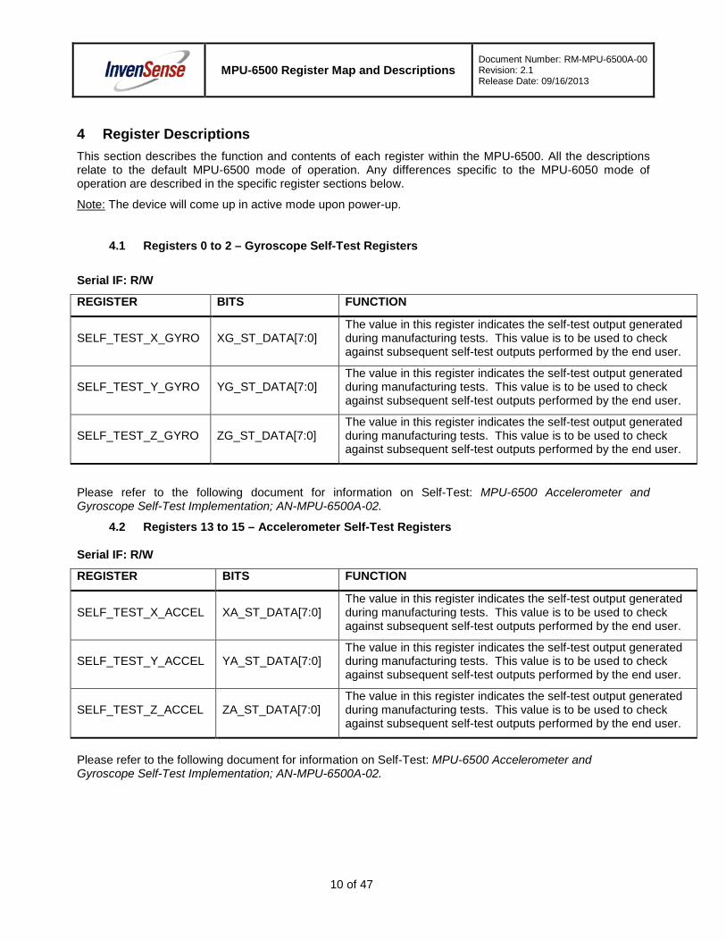
4.1 Registers 0 to 2 – Gyroscope Self-Test Registers
Serial IF: R/W
REGISTER BITS FUNCTION
SELF_TEST_X_GYRO XG_ST_DATA[7:0] The value in this register indicates the self-test output generated during manufacturing tests. This value is to be used to check against subsequent self-test outputs performed by the end user.
SELF_TEST_Y_GYRO YG_ST_DATA[7:0] The value in this register indicates the self-test output generated during manufacturing tests. This value is to be used to check against subsequent self-test outputs performed by the end user.
SELF_TEST_Z_GYRO ZG_ST_DATA[7:0] The value in this register indicates the self-test output generated during manufacturing tests. This value is to be used to check against subsequent self-test outputs performed by the end user.
Please refer to the following document for information on Self-Test: MPU-6500 Accelerometer and Gyroscope Self-Test Implementation; AN-MPU-6500A-02.
4.2 Registers 13 to 15 – Accelerometer Self-Test Registers Serial IF: R/W
REGISTER BITS FUNCTION
SELF_TEST_X_ACCEL XA_ST_DATA[7:0] The value in this register indicates the self-test output generated during manufacturing tests. This value is to be used to check against subsequent self-test outputs performed by the end user.
SELF_TEST_Y_ACCEL YA_ST_DATA[7:0] The value in this register indicates the self-test output generated during manufacturing tests. This value is to be used to check against subsequent self-test outputs performed by the end user.
SELF_TEST_Z_ACCEL ZA_ST_DATA[7:0] The value in this register indicates the self-test output generated during manufacturing tests. This value is to be used to check against subsequent self-test outputs performed by the end user.
Please refer to the following document for information on Self-Test: MPU-6500 Accelerometer and Gyroscope Self-Test Implementation; AN-MPU-6500A-02.
10 of 47
MPU-6500 Register Map and Descriptions
Document Number: RM-MPU-6500A-00 Revision: 2.1 Release Date: 09/16/2013
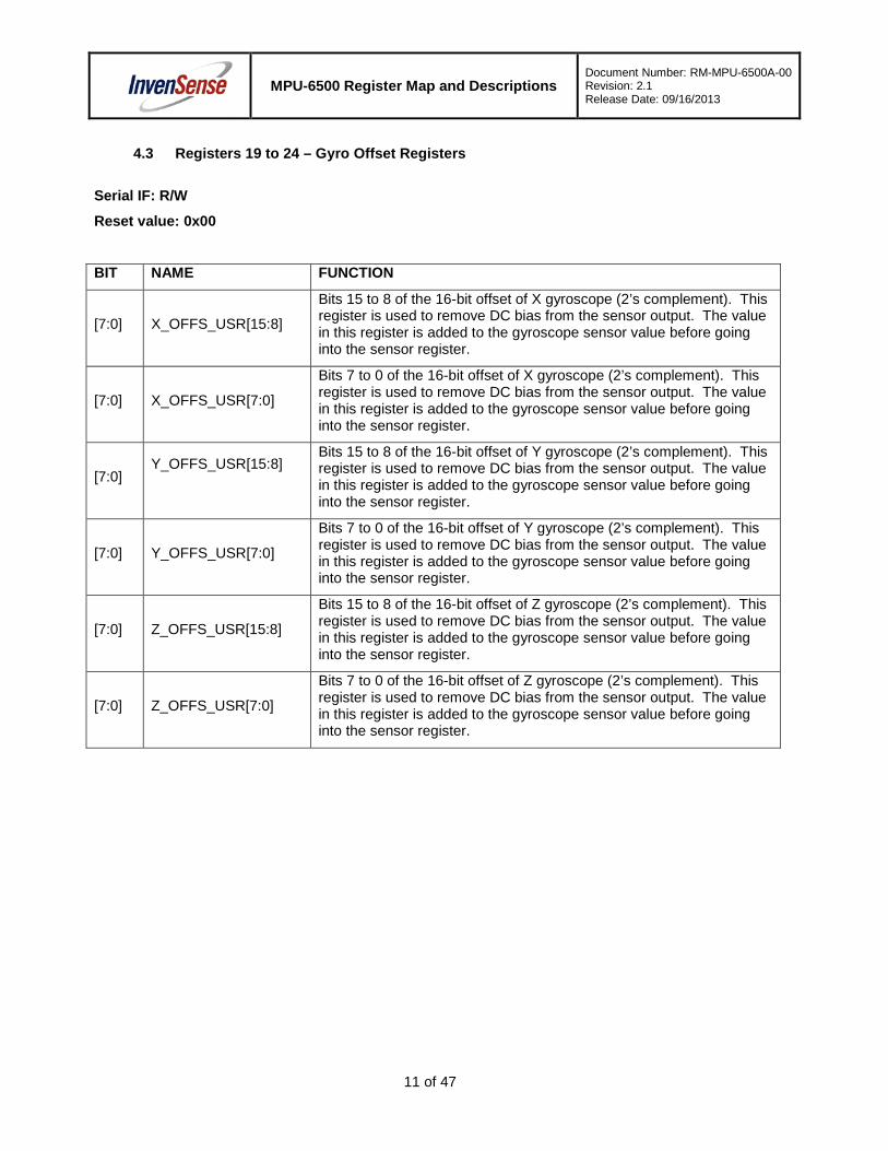
4.3 Registers 19 to 24 – Gyro Offset Registers
Serial IF: R/W
Reset value: 0x00
BIT NAME FUNCTION
[7:0] X_OFFS_USR[15:8] Bits 15 to 8 of the 16-bit offset of X gyroscope (2’s complement). This register is used to remove DC bias from the sensor output. The value in this register is added to the gyroscope sensor value before going into the sensor register.
[7:0] X_OFFS_USR[7:0] Bits 7 to 0 of the 16-bit offset of X gyroscope (2’s complement). This register is used to remove DC bias from the sensor output. The value in this register is added to the gyroscope sensor value before going into the sensor register.
[7:0] Y_OFFS_USR[15:8]
Bits 15 to 8 of the 16-bit offset of Y gyroscope (2’s complement). This register is used to remove DC bias from the sensor output. The value in this register is added to the gyroscope sensor value before going into the sensor register.
[7:0] Y_OFFS_USR[7:0] Bits 7 to 0 of the 16-bit offset of Y gyroscope (2’s complement). This register is used to remove DC bias from the sensor output. The value in this register is added to the gyroscope sensor value before going into the sensor register.
[7:0] Z_OFFS_USR[15:8] Bits 15 to 8 of the 16-bit offset of Z gyroscope (2’s complement). This register is used to remove DC bias from the sensor output. The value in this register is added to the gyroscope sensor value before going into the sensor register.
[7:0] Z_OFFS_USR[7:0] Bits 7 to 0 of the 16-bit offset of Z gyroscope (2’s complement). This register is used to remove DC bias from the sensor output. The value in this register is added to the gyroscope sensor value before going into the sensor register.
11 of 47
MPU-6500 Register Map and Descriptions
Document Number: RM-MPU-6500A-00 Revision: 2.1 Release Date: 09/16/2013
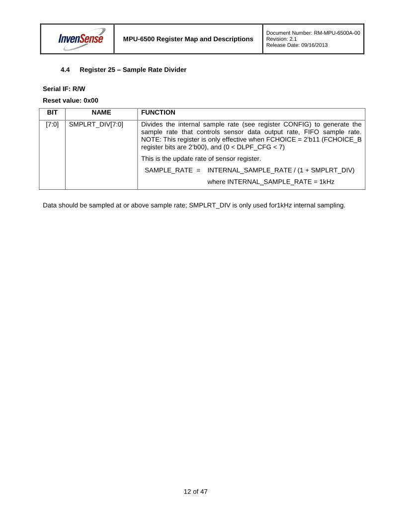
4.4 Register 25 – Sample Rate Divider
Serial IF: R/W
Reset value: 0x00
BIT NAME FUNCTION
[7:0] SMPLRT_DIV[7:0] Divides the internal sample rate (see register CONFIG) to generate the sample rate that controls sensor data output rate, FIFO sample rate. NOTE: This register is only effective when FCHOICE = 2’b11 (FCHOICE_B register bits are 2’b00), and (0 < DLPF_CFG < 7)
This is the update rate of sensor register.
SAMPLE_RATE = INTERNAL_SAMPLE_RATE / (1 + SMPLRT_DIV)
where INTERNAL_SAMPLE_RATE = 1kHz
Data should be sampled at or above sample rate; SMPLRT_DIV is only used for1kHz internal sampling.
12 of 47
MPU-6500 Register Map and Descriptions
Document Number: RM-MPU-6500A-00 Revision: 2.1 Release Date: 09/16/2013
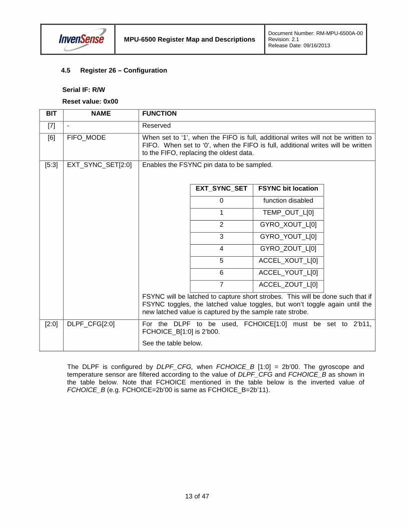
4.5 Register 26 – Configuration
Serial IF: R/W
Reset value: 0x00
BIT NAME FUNCTION
[7] - Reserved
[6] FIFO_MODE When set to ‘1’, when the FIFO is full, additional writes will not be written to FIFO. When set to ‘0’, when the FIFO is full, additional writes will be written to the FIFO, replacing the oldest data.
[5:3] EXT_SYNC_SET[2:0] Enables the FSYNC pin data to be sampled.
EXT_SYNC_SET FSYNC bit location
0 function disabled 1 TEMP_OUT_L[0] 2 GYRO_XOUT_L[0] 3 GYRO_YOUT_L[0] 4 GYRO_ZOUT_L[0] 5 ACCEL_XOUT_L[0] 6 ACCEL_YOUT_L[0] 7 ACCEL_ZOUT_L[0]
FSYNC will be latched to capture short strobes. This will be done such that if FSYNC toggles, the latched value toggles, but won’t toggle again until the new latched value is captured by the sample rate strobe.
[2:0] DLPF_CFG[2:0] For the DLPF to be used, FCHOICE[1:0] must be set to 2’b11, FCHOICE_B[1:0] is 2’b00.
See the table below.
The DLPF is configured by DLPF_CFG, when FCHOICE_B [1:0] = 2b’00. The gyroscope and temperature sensor are filtered according to the value of DLPF_CFG and FCHOICE_B as shown in the table below. Note that FCHOICE mentioned in the table below is the inverted value of FCHOICE_B (e.g. FCHOICE=2b’00 is same as FCHOICE_B=2b’11).
13 of 47
MPU-6500 Register Map and Descriptions
Document Number: RM-MPU-6500A-00 Revision: 2.1 Release Date: 09/16/2013
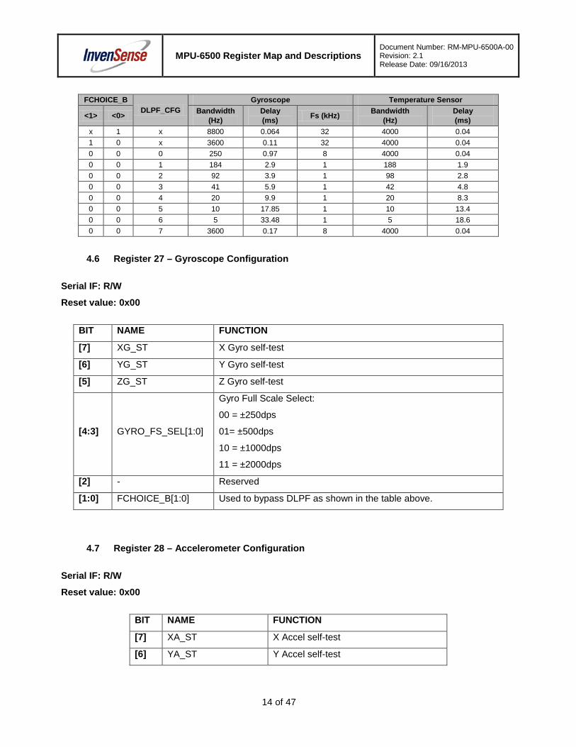
FCHOICE_B DLPF_CFG
Gyroscope Temperature Sensor
<1> <0> Bandwidth (Hz)
Delay (ms) Fs (kHz) Bandwidth
(Hz) Delay (ms)
x 1 x 8800 0.064 32 4000 0.04 1 0 x 3600 0.11 32 4000 0.04 0 0 0 250 0.97 8 4000 0.04 0 0 1 184 2.9 1 188 1.9 0 0 2 92 3.9 1 98 2.8 0 0 3 41 5.9 1 42 4.8 0 0 4 20 9.9 1 20 8.3 0 0 5 10 17.85 1 10 13.4 0 0 6 5 33.48 1 5 18.6 0 0 7 3600 0.17 8 4000 0.04
4.6 Register 27 – Gyroscope Configuration
Serial IF: R/W
Reset value: 0x00
BIT NAME FUNCTION
[7] XG_ST X Gyro self-test [6] YG_ST Y Gyro self-test [5] ZG_ST Z Gyro self-test
[4:3] GYRO_FS_SEL[1:0]
Gyro Full Scale Select: 00 = ±250dps 01= ±500dps 10 = ±1000dps 11 = ±2000dps
[2] - Reserved [1:0] FCHOICE_B[1:0] Used to bypass DLPF as shown in the table above.
4.7 Register 28 – Accelerometer Configuration
Serial IF: R/W
Reset value: 0x00
BIT NAME FUNCTION [7] XA_ST X Accel self-test [6] YA_ST Y Accel self-test
14 of 47
MPU-6500 Register Map and Descriptions
Document Number: RM-MPU-6500A-00 Revision: 2.1 Release Date: 09/16/2013
[5] ZA_ST Z Accel self-test
[4:3] ACCEL_FS_SEL[1:0] Accel Full Scale Select: ±2g (00), ±4g (01), ±8g (10), ±16g (11)
[2:0] - Reserved
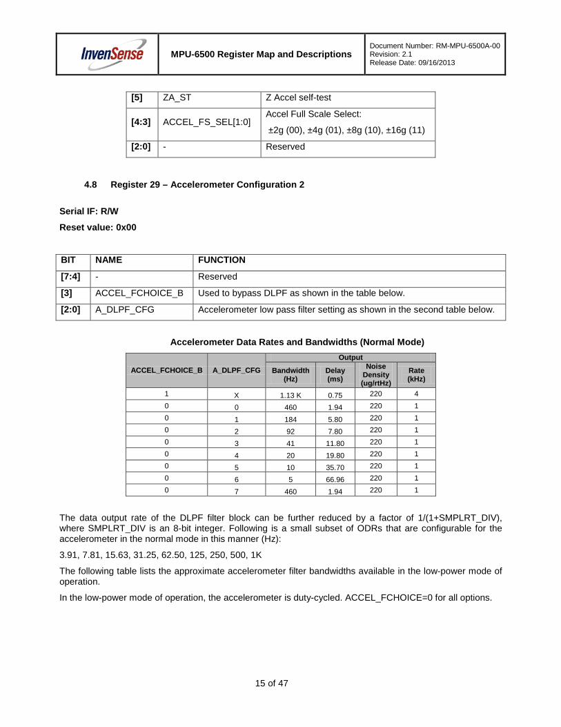
4.8 Register 29 – Accelerometer Configuration 2
Serial IF: R/W
Reset value: 0x00
BIT NAME FUNCTION
[7:4] - Reserved
[3] ACCEL_FCHOICE_B Used to bypass DLPF as shown in the table below. [2:0] A_DLPF_CFG Accelerometer low pass filter setting as shown in the second table below.
Accelerometer Data Rates and Bandwidths (Normal Mode)
ACCEL_FCHOICE_B A_DLPF_CFG
Output
Bandwidth (Hz)
Delay (ms)
Noise Density (ug/rtHz)
Rate (kHz)
1 X 1.13 K 0.75 220 4 0 0 460 1.94 220 1 0 1 184 5.80 220 1 0 2 92 7.80 220 1 0 3 41 11.80 220 1 0 4 20 19.80 220 1 0 5 10 35.70 220 1 0 6 5 66.96 220 1 0 7 460 1.94 220 1
The data output rate of the DLPF filter block can be further reduced by a factor of 1/(1+SMPLRT_DIV), where SMPLRT_DIV is an 8-bit integer. Following is a small subset of ODRs that are configurable for the accelerometer in the normal mode in this manner (Hz):
3.91, 7.81, 15.63, 31.25, 62.50, 125, 250, 500, 1K
The following table lists the approximate accelerometer filter bandwidths available in the low-power mode of operation.
In the low-power mode of operation, the accelerometer is duty-cycled. ACCEL_FCHOICE=0 for all options.
15 of 47
MPU-6500 Register Map and Descriptions
Document Number: RM-MPU-6500A-00 Revision: 2.1 Release Date: 09/16/2013
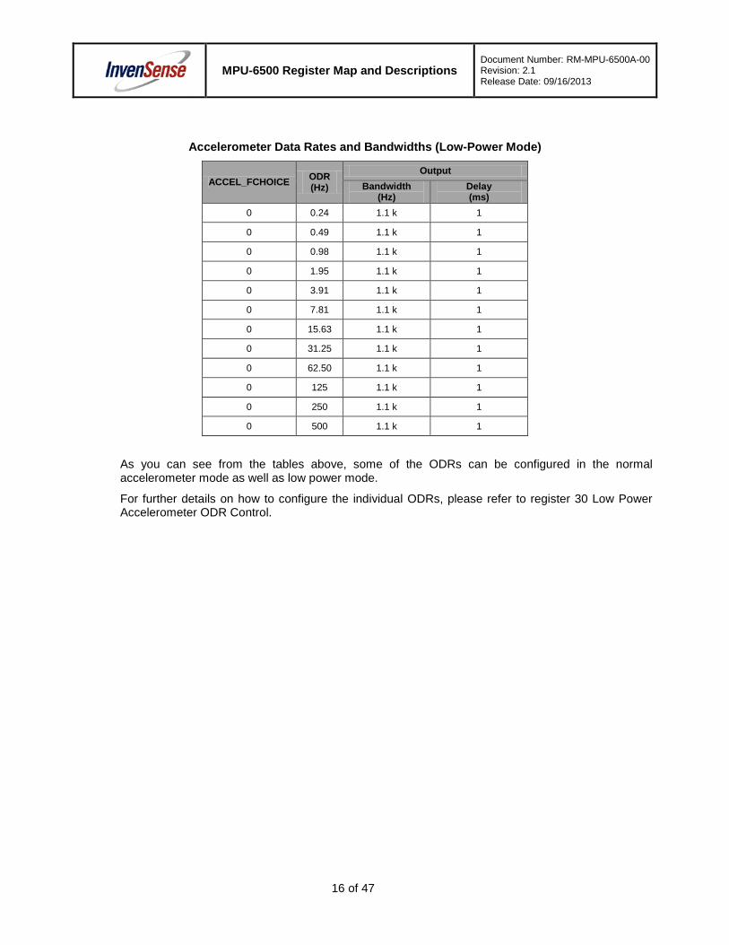
Accelerometer Data Rates and Bandwidths (Low-Power Mode)
ACCEL_FCHOICE ODR (Hz)
Output Bandwidth
(Hz) Delay (ms)
0 0.24 1.1 k 1
0 0.49 1.1 k 1
0 0.98 1.1 k 1
0 1.95 1.1 k 1
0 3.91 1.1 k 1
0 7.81 1.1 k 1
0 15.63 1.1 k 1
0 31.25 1.1 k 1
0 62.50 1.1 k 1
0 125 1.1 k 1
0 250 1.1 k 1
0 500 1.1 k 1
As you can see from the tables above, some of the ODRs can be configured in the normal accelerometer mode as well as low power mode.
For further details on how to configure the individual ODRs, please refer to register 30 Low Power Accelerometer ODR Control.
16 of 47
MPU-6500 Register Map and Descriptions
Document Number: RM-MPU-6500A-00 Revision: 2.1 Release Date: 09/16/2013
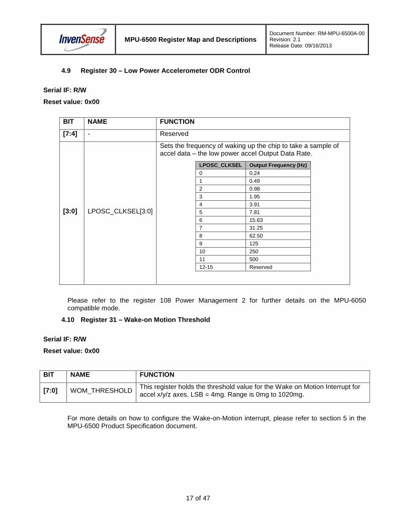
4.9 Register 30 – Low Power Accelerometer ODR Control
Serial IF: R/W
Reset value: 0x00
BIT NAME FUNCTION
[7:4] - Reserved
[3:0] LPOSC_CLKSEL[3:0]
Sets the frequency of waking up the chip to take a sample of accel data – the low power accel Output Data Rate.
LPOSC_CLKSEL Output Frequency (Hz) 0 0.24 1 0.49 2 0.98 3 1.95 4 3.91 5 7.81 6 15.63 7 31.25 8 62.50 9 125 10 250 11 500 12-15 Reserved
Please refer to the register 108 Power Management 2 for further details on the MPU-6050 compatible mode.
4.10 Register 31 – Wake-on Motion Threshold
Serial IF: R/W
Reset value: 0x00
BIT NAME FUNCTION
[7:0] WOM_THRESHOLD This register holds the threshold value for the Wake on Motion Interrupt for accel x/y/z axes. LSB = 4mg. Range is 0mg to 1020mg.
For more details on how to configure the Wake-on-Motion interrupt, please refer to section 5 in the MPU-6500 Product Specification document.
17 of 47
MPU-6500 Register Map and Descriptions
Document Number: RM-MPU-6500A-00 Revision: 2.1 Release Date: 09/16/2013
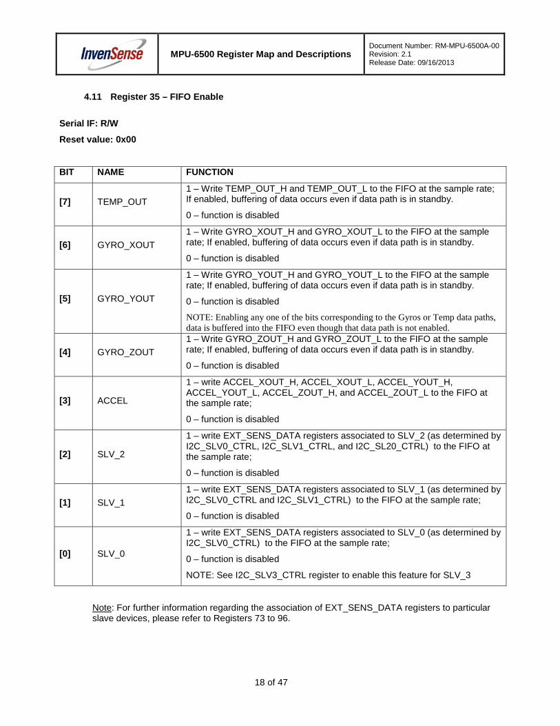
4.11 Register 35 – FIFO Enable
Serial IF: R/W
Reset value: 0x00
BIT NAME FUNCTION
[7] TEMP_OUT 1 – Write TEMP_OUT_H and TEMP_OUT_L to the FIFO at the sample rate; If enabled, buffering of data occurs even if data path is in standby. 0 – function is disabled
[6] GYRO_XOUT 1 – Write GYRO_XOUT_H and GYRO_XOUT_L to the FIFO at the sample rate; If enabled, buffering of data occurs even if data path is in standby. 0 – function is disabled
[5] GYRO_YOUT
1 – Write GYRO_YOUT_H and GYRO_YOUT_L to the FIFO at the sample rate; If enabled, buffering of data occurs even if data path is in standby. 0 – function is disabled NOTE: Enabling any one of the bits corresponding to the Gyros or Temp data paths, data is buffered into the FIFO even though that data path is not enabled.
[4] GYRO_ZOUT 1 – Write GYRO_ZOUT_H and GYRO_ZOUT_L to the FIFO at the sample rate; If enabled, buffering of data occurs even if data path is in standby. 0 – function is disabled
[3] ACCEL
1 – write ACCEL_XOUT_H, ACCEL_XOUT_L, ACCEL_YOUT_H, ACCEL_YOUT_L, ACCEL_ZOUT_H, and ACCEL_ZOUT_L to the FIFO at the sample rate; 0 – function is disabled
[2] SLV_2
1 – write EXT_SENS_DATA registers associated to SLV_2 (as determined by I2C_SLV0_CTRL, I2C_SLV1_CTRL, and I2C_SL20_CTRL) to the FIFO at the sample rate; 0 – function is disabled
[1] SLV_1 1 – write EXT_SENS_DATA registers associated to SLV_1 (as determined by I2C_SLV0_CTRL and I2C_SLV1_CTRL) to the FIFO at the sample rate; 0 – function is disabled
[0] SLV_0
1 – write EXT_SENS_DATA registers associated to SLV_0 (as determined by I2C_SLV0_CTRL) to the FIFO at the sample rate; 0 – function is disabled NOTE: See I2C_SLV3_CTRL register to enable this feature for SLV_3
Note: For further information regarding the association of EXT_SENS_DATA registers to particular slave devices, please refer to Registers 73 to 96.
18 of 47
MPU-6500 Register Map and Descriptions
Document Number: RM-MPU-6500A-00 Revision: 2.1 Release Date: 09/16/2013
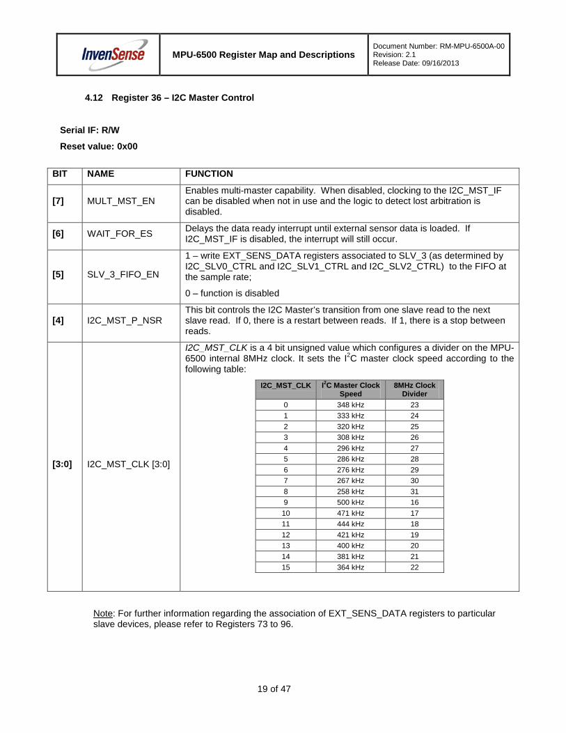
4.12 Register 36 – I2C Master Control
Serial IF: R/W
Reset value: 0x00
BIT NAME FUNCTION
[7] MULT_MST_EN Enables multi-master capability. When disabled, clocking to the I2C_MST_IF can be disabled when not in use and the logic to detect lost arbitration is disabled.
[6] WAIT_FOR_ES Delays the data ready interrupt until external sensor data is loaded. If I2C_MST_IF is disabled, the interrupt will still occur.
[5] SLV_3_FIFO_EN
1 – write EXT_SENS_DATA registers associated to SLV_3 (as determined by I2C_SLV0_CTRL and I2C_SLV1_CTRL and I2C_SLV2_CTRL) to the FIFO at the sample rate; 0 – function is disabled
[4] I2C_MST_P_NSR This bit controls the I2C Master’s transition from one slave read to the next slave read. If 0, there is a restart between reads. If 1, there is a stop between reads.
[3:0] I2C_MST_CLK [3:0]
I2C_MST_CLK is a 4 bit unsigned value which configures a divider on the MPU-6500 internal 8MHz clock. It sets the I2C master clock speed according to the following table:
I2C_MST_CLK I2C Master Clock Speed
8MHz Clock Divider
0 348 kHz 23 1 333 kHz 24 2 320 kHz 25 3 308 kHz 26 4 296 kHz 27 5 286 kHz 28 6 276 kHz 29 7 267 kHz 30 8 258 kHz 31 9 500 kHz 16 10 471 kHz 17 11 444 kHz 18 12 421 kHz 19 13 400 kHz 20 14 381 kHz 21 15 364 kHz 22
Note: For further information regarding the association of EXT_SENS_DATA registers to particular slave devices, please refer to Registers 73 to 96.
19 of 47
MPU-6500 Register Map and Descriptions
Document Number: RM-MPU-6500A-00 Revision: 2.1 Release Date: 09/16/2013
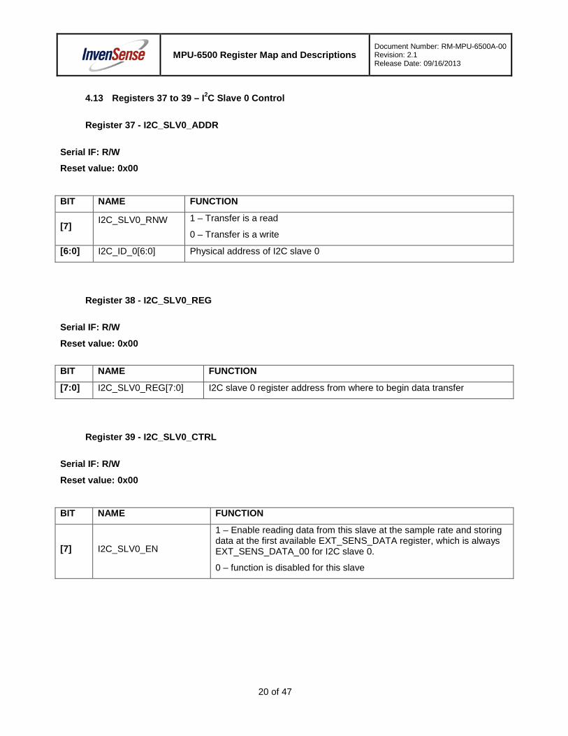
4.13 Registers 37 to 39 – I2C Slave 0 Control
Register 37 - I2C_SLV0_ADDR
Serial IF: R/W
Reset value: 0x00
BIT NAME FUNCTION
[7] I2C_SLV0_RNW
1 – Transfer is a read 0 – Transfer is a write
[6:0] I2C_ID_0[6:0] Physical address of I2C slave 0
Register 38 - I2C_SLV0_REG
Serial IF: R/W
Reset value: 0x00
BIT NAME FUNCTION
[7:0] I2C_SLV0_REG[7:0] I2C slave 0 register address from where to begin data transfer
Register 39 - I2C_SLV0_CTRL
Serial IF: R/W
Reset value: 0x00
BIT NAME FUNCTION
[7] I2C_SLV0_EN
1 – Enable reading data from this slave at the sample rate and storing data at the first available EXT_SENS_DATA register, which is always EXT_SENS_DATA_00 for I2C slave 0. 0 – function is disabled for this slave
20 of 47
MPU-6500 Register Map and Descriptions
Document Number: RM-MPU-6500A-00 Revision: 2.1 Release Date: 09/16/2013
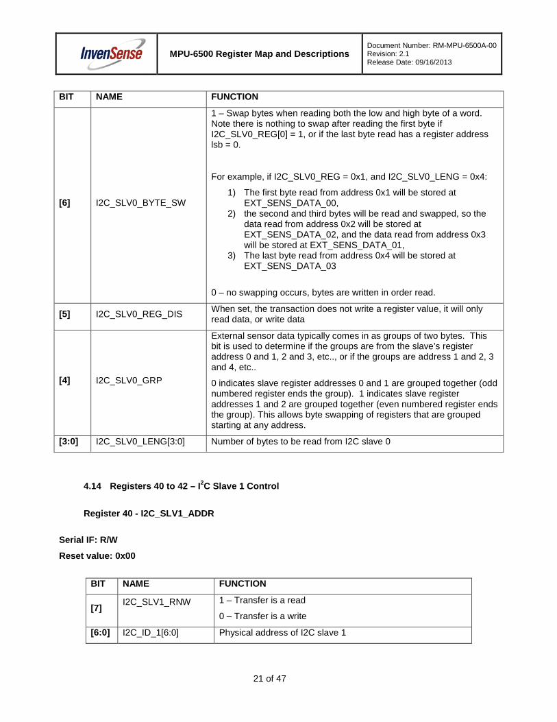
BIT NAME FUNCTION
[6] I2C_SLV0_BYTE_SW
1 – Swap bytes when reading both the low and high byte of a word. Note there is nothing to swap after reading the first byte if I2C_SLV0_REG[0] = 1, or if the last byte read has a register address lsb = 0.
For example, if I2C_SLV0_REG = 0x1, and I2C_SLV0_LENG = 0x4:
1) The first byte read from address 0x1 will be stored at EXT_SENS_DATA_00,
2) the second and third bytes will be read and swapped, so the data read from address 0x2 will be stored at EXT_SENS_DATA_02, and the data read from address 0x3 will be stored at EXT_SENS_DATA_01,
3) The last byte read from address 0x4 will be stored at EXT_SENS_DATA_03
0 – no swapping occurs, bytes are written in order read.
[5] I2C_SLV0_REG_DIS When set, the transaction does not write a register value, it will only read data, or write data
[4] I2C_SLV0_GRP
External sensor data typically comes in as groups of two bytes. This bit is used to determine if the groups are from the slave’s register address 0 and 1, 2 and 3, etc.., or if the groups are address 1 and 2, 3 and 4, etc.. 0 indicates slave register addresses 0 and 1 are grouped together (odd numbered register ends the group). 1 indicates slave register addresses 1 and 2 are grouped together (even numbered register ends the group). This allows byte swapping of registers that are grouped starting at any address.
[3:0] I2C_SLV0_LENG[3:0] Number of bytes to be read from I2C slave 0
4.14 Registers 40 to 42 – I2C Slave 1 Control
Register 40 - I2C_SLV1_ADDR
Serial IF: R/W
Reset value: 0x00
BIT NAME FUNCTION
[7] I2C_SLV1_RNW
1 – Transfer is a read 0 – Transfer is a write
[6:0] I2C_ID_1[6:0] Physical address of I2C slave 1
21 of 47
MPU-6500 Register Map and Descriptions
Document Number: RM-MPU-6500A-00 Revision: 2.1 Release Date: 09/16/2013
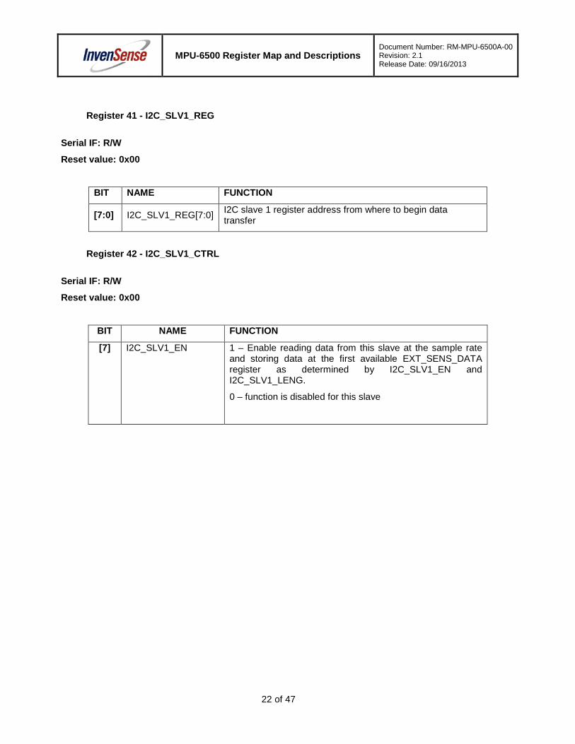
Register 41 - I2C_SLV1_REG
Serial IF: R/W
Reset value: 0x00
BIT NAME FUNCTION
[7:0] I2C_SLV1_REG[7:0] I2C slave 1 register address from where to begin data transfer
Register 42 - I2C_SLV1_CTRL
Serial IF: R/W
Reset value: 0x00
BIT NAME FUNCTION
[7] I2C_SLV1_EN 1 – Enable reading data from this slave at the sample rate and storing data at the first available EXT_SENS_DATA register as determined by I2C_SLV1_EN and I2C_SLV1_LENG.
0 – function is disabled for this slave
22 of 47
MPU-6500 Register Map and Descriptions
Document Number: RM-MPU-6500A-00 Revision: 2.1 Release Date: 09/16/2013
BIT NAME FUNCTION
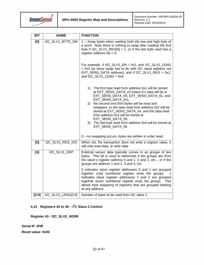
[6] I2C_SLV1_BYTE_SW 1 – Swap bytes when reading both the low and high byte of a word. Note there is nothing to swap after reading the first byte if I2C_SLV1_REG[0] = 1, or if the last byte read has a register address lsb = 0.
For example, if I2C_SLV1_EN = 0x1, and I2C_SLV1_LENG = 0x3 (to show swap has to do with I2C slave address not EXT_SENS_DATA address), and if I2C_SLV1_REG = 0x1, and I2C_SLV1_LENG = 0x4:
1) The first byte read from address 0x1 will be stored at EXT_SENS_DATA_03 (slave 0’s data will be in EXT_SENS_DATA_00, EXT_SENS_DATA_01, and EXT_SENS_DATA_02),
2) the second and third bytes will be read and swapped, so the data read from address 0x2 will be stored at EXT_SENS_DATA_04, and the data read from address 0x3 will be stored at EXT_SENS_DATA_05,
3) The last byte read from address 0x4 will be stored at EXT_SENS_DATA_06
0 – no swapping occurs, bytes are written in order read.
[5] I2C_SLV1_REG_DIS When set, the transaction does not write a register value, it will only read data, or write data
[4] I2C_SLV1_GRP External sensor data typically comes in as groups of two bytes. This bit is used to determine if the groups are from the slave’s register address 0 and 1, 2 and 3, etc.., or if the groups are address 1 and 2, 3 and 4, etc.
0 indicates slave register addresses 0 and 1 are grouped together (odd numbered register ends the group). 1 indicates slave register addresses 1 and 2 are grouped together (even numbered register ends the group). This allows byte swapping of registers that are grouped starting at any address.
[3:0] I2C_SLV1_LENG[3:0] Number of bytes to be read from I2C slave 1
4.15 Registers 43 to 45 – I2C Slave 2 Control
Register 43 - I2C_SLV2_ADDR
Serial IF: R/W
Reset value: 0x00
23 of 47

MPU-6500 Register Map and Descriptions
Document Number: RM-MPU-6500A-00 Revision: 2.1 Release Date: 09/16/2013
BIT NAME FUNCTION
[7] I2C_SLV2_RNW
1 – Transfer is a read 0 – Transfer is a write
[6:0] I2C_ID_2[6:0] Physical address of I2C slave 2
Register 44 - I2C_SLV2_REG
Serial IF: R/W
Reset value: 0x00
BIT NAME FUNCTION
[7:0] I2C_SLV2_REG[7:0] I2C slave 2 register address from where to begin data transfer.
Register 45 - I2C_SLV2_CTRL
Serial IF: R/W
Reset value: 0x00
BIT NAME FUNCTION
[7] I2C_SLV2_EN
1 – Enable reading data from this slave at the sample rate and storing data at the first available EXT_SENS_DATA register as determined by I2C_SLV0_EN, I2C_SLV0_LENG, I2C_SLV1_EN and I2C_SLV1_LENG. 0 – function is disabled for this slave
[6] I2C_SLV2_BYTE_SW
1 – Swap bytes when reading both the low and high byte of a word. Note there is nothing to swap after reading the first byte if I2C_SLV2_REG[0] = 1, or if the last byte read has a register address LSB = 0. See I2C_SLV1_CTRL for an example. 0 – no swapping occurs, bytes are written in order read.
[5] I2C_SLV2_REG_DIS When set, the transaction does not write a register value, it will only read data, or write data
24 of 47
MPU-6500 Register Map and Descriptions
Document Number: RM-MPU-6500A-00 Revision: 2.1 Release Date: 09/16/2013
BIT NAME FUNCTION
[4] I2C_SLV2_GRP
External sensor data typically comes in as groups of two bytes. This bit is used to determine if the groups are from the slave’s register address 0 and 1, 2 and 3, etc., or if the groups are address 1 and 2, 3 and 4, etc. 0 indicates slave register addresses 0 and 1 are grouped together (odd numbered register ends the group). 1 indicates slave register addresses 1 and 2 are grouped together (even numbered register ends the group). This allows byte swapping of registers that are grouped starting at any address.
[3:0] I2C_SLV2_LENG[3:0] Number of bytes to be read from I2C slave 2
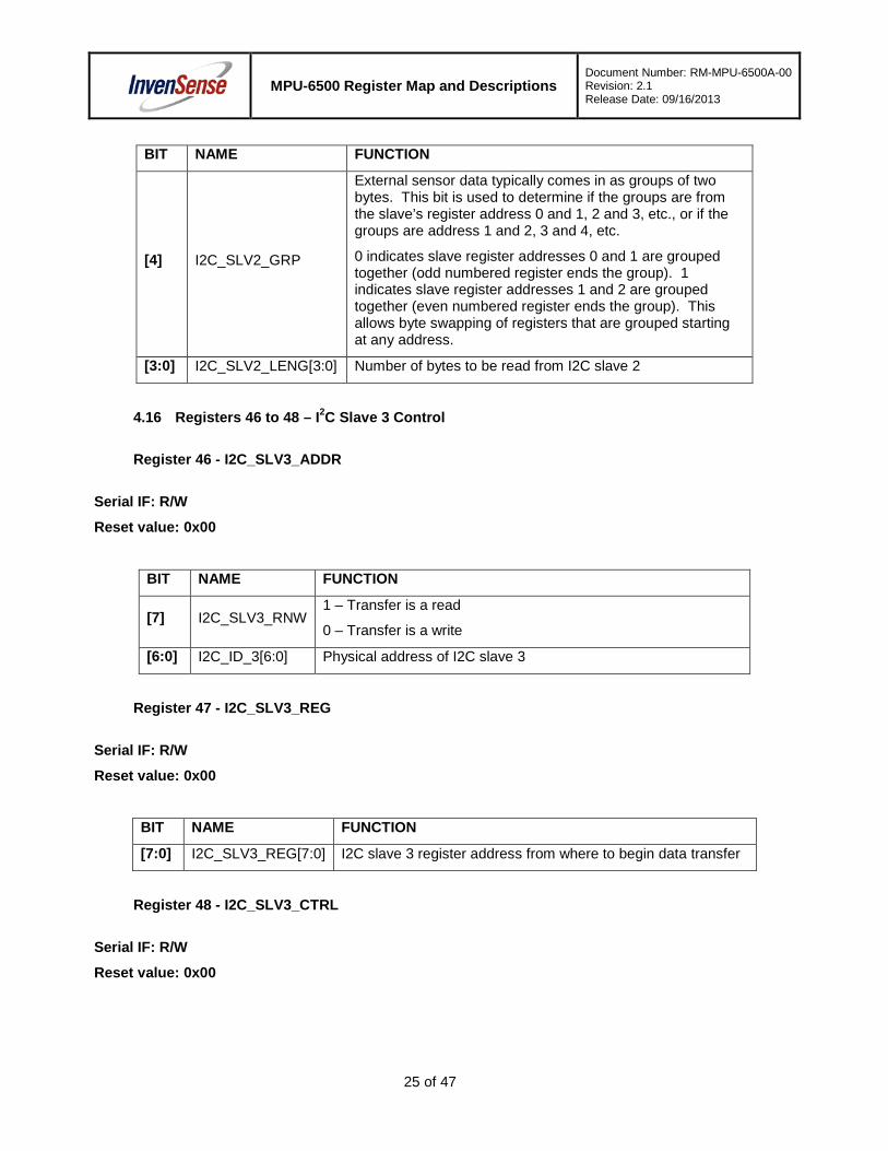
4.16 Registers 46 to 48 – I2C Slave 3 Control
Register 46 - I2C_SLV3_ADDR
Serial IF: R/W
Reset value: 0x00
BIT NAME FUNCTION
[7] I2C_SLV3_RNW 1 – Transfer is a read 0 – Transfer is a write
[6:0] I2C_ID_3[6:0] Physical address of I2C slave 3
Register 47 - I2C_SLV3_REG
Serial IF: R/W
Reset value: 0x00
BIT NAME FUNCTION
[7:0] I2C_SLV3_REG[7:0] I2C slave 3 register address from where to begin data transfer
Register 48 - I2C_SLV3_CTRL
Serial IF: R/W
Reset value: 0x00
25 of 47

MPU-6500 Register Map and Descriptions
Document Number: RM-MPU-6500A-00 Revision: 2.1 Release Date: 09/16/2013
BIT NAME FUNCTION
[7] I2C_SLV3_EN
1 – Enable reading data from this slave at the sample rate and storing data at the first available EXT_SENS_DATA register as determined by I2C_SLV0_EN, I2C_SLV0_LENG, I2C_SLV1_EN, I2C_SLV1_LENG, I2C_SLV2_EN and I2C_SLV2_LENG. 0 – function is disabled for this slave
[6] I2C_SLV3_BYTE_SW
1 – Swap bytes when reading both the low and high byte of a word. Note there is nothing to swap after reading the first byte if I2C_SLV3_REG[0] = 1, or if the last byte read has a register address LSB = 0. See I2C_SLV1_CTRL for an example. 0 – no swapping occurs, bytes are written in order read.
[5] I2C_SLV0_REG_DIS When set, the transaction does not write a register value, it will only read data, or write data
[4] I2C_SLV3_GRP
External sensor data typically comes in as groups of two bytes. This bit is used to determine if the groups are from the slave’s register address 0 and 1, 2 and 3, etc.., or if the groups are address 1 and 2, 3 and 4, etc. 0 indicates slave register addresses 0 and 1 are grouped together (odd numbered register ends the group). 1 indicates slave register addresses 1 and 2 are grouped together (even numbered register ends the group). This allows byte swapping of registers that are grouped starting at any address.
[3:0] I2C_SLV3_LENG[3:0] Number of bytes to be read from I2C slave 3
4.17 Registers 49 to 53 – I2C Slave 4 Control
Register 49 - I2C_SLV4_ADDR
Serial IF: R/W
Reset value: 0x00
BIT NAME FUNCTION
[7] I2C_SLV4_RNW 1 – Transfer is a read 0 – Transfer is a write
[6:0] I2C_ID_4[6:0] Physical address of I2C slave 4
Register 50 - I2C_SLV4_REG
Serial IF: R/W
Reset value: 0x00
26 of 47
MPU-6500 Register Map and Descriptions
Document Number: RM-MPU-6500A-00 Revision: 2.1 Release Date: 09/16/2013
BIT NAME FUNCTION
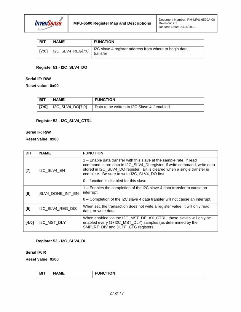
[7:0] I2C_SLV4_REG[7:0] I2C slave 4 register address from where to begin data transfer
Register 51 - I2C_SLV4_DO
Serial IF: R/W
Reset value: 0x00
BIT NAME FUNCTION
[7:0] I2C_SLV4_DO[7:0] Data to be written to I2C Slave 4 if enabled.
Register 52 - I2C_SLV4_CTRL
Serial IF: R/W
Reset value: 0x00
BIT NAME FUNCTION
[7] I2C_SLV4_EN
1 – Enable data transfer with this slave at the sample rate. If read command, store data in I2C_SLV4_DI register, if write command, write data stored in I2C_SLV4_DO register. Bit is cleared when a single transfer is complete. Be sure to write I2C_SLV4_DO first 0 – function is disabled for this slave
[6] SLV4_DONE_INT_EN 1 – Enables the completion of the I2C slave 4 data transfer to cause an interrupt. 0 – Completion of the I2C slave 4 data transfer will not cause an interrupt.
[5] I2C_SLV4_REG_DIS When set, the transaction does not write a register value, it will only read data, or write data
[4:0] I2C_MST_DLY When enabled via the I2C_MST_DELAY_CTRL, those slaves will only be enabled every (1+I2C_MST_DLY) samples (as determined by the SMPLRT_DIV and DLPF_CFG registers.
Register 53 - I2C_SLV4_DI
Serial IF: R
Reset value: 0x00
BIT NAME FUNCTION
27 of 47
MPU-6500 Register Map and Descriptions
Document Number: RM-MPU-6500A-00 Revision: 2.1 Release Date: 09/16/2013
BIT NAME FUNCTION
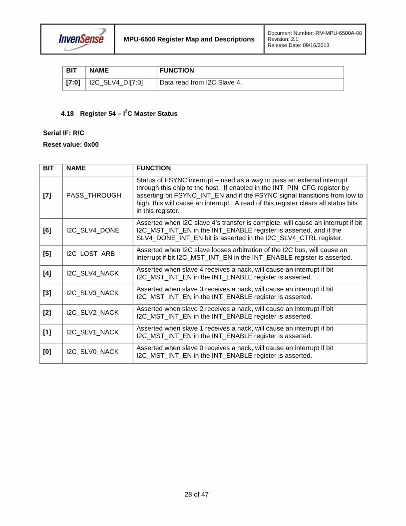
[7:0] I2C_SLV4_DI[7:0] Data read from I2C Slave 4.
4.18 Register 54 – I2C Master Status
Serial IF: R/C
Reset value: 0x00
BIT NAME FUNCTION
[7] PASS_THROUGH
Status of FSYNC interrupt – used as a way to pass an external interrupt through this chip to the host. If enabled in the INT_PIN_CFG register by asserting bit FSYNC_INT_EN and if the FSYNC signal transitions from low to high, this will cause an interrupt. A read of this register clears all status bits in this register.
[6] I2C_SLV4_DONE Asserted when I2C slave 4’s transfer is complete, will cause an interrupt if bit I2C_MST_INT_EN in the INT_ENABLE register is asserted, and if the SLV4_DONE_INT_EN bit is asserted in the I2C_SLV4_CTRL register.
[5] I2C_LOST_ARB Asserted when I2C slave looses arbitration of the I2C bus, will cause an interrupt if bit I2C_MST_INT_EN in the INT_ENABLE register is asserted.
[4] I2C_SLV4_NACK Asserted when slave 4 receives a nack, will cause an interrupt if bit I2C_MST_INT_EN in the INT_ENABLE register is asserted.
[3] I2C_SLV3_NACK Asserted when slave 3 receives a nack, will cause an interrupt if bit I2C_MST_INT_EN in the INT_ENABLE register is asserted.
[2] I2C_SLV2_NACK Asserted when slave 2 receives a nack, will cause an interrupt if bit I2C_MST_INT_EN in the INT_ENABLE register is asserted.
[1] I2C_SLV1_NACK Asserted when slave 1 receives a nack, will cause an interrupt if bit I2C_MST_INT_EN in the INT_ENABLE register is asserted.
[0] I2C_SLV0_NACK Asserted when slave 0 receives a nack, will cause an interrupt if bit I2C_MST_INT_EN in the INT_ENABLE register is asserted.
28 of 47
MPU-6500 Register Map and Descriptions
Document Number: RM-MPU-6500A-00 Revision: 2.1 Release Date: 09/16/2013
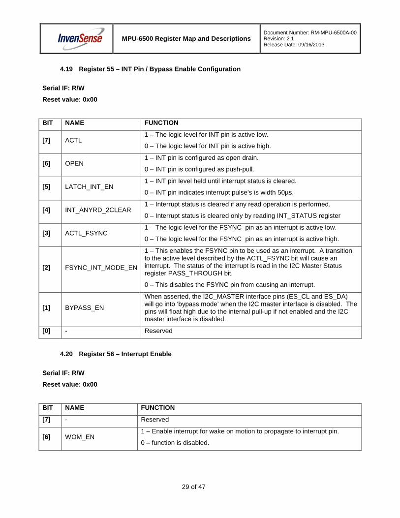
4.19 Register 55 – INT Pin / Bypass Enable Configuration
Serial IF: R/W
Reset value: 0x00
BIT NAME FUNCTION
[7] ACTL 1 – The logic level for INT pin is active low. 0 – The logic level for INT pin is active high.
[6] OPEN 1 – INT pin is configured as open drain. 0 – INT pin is configured as push-pull.
[5] LATCH_INT_EN 1 – INT pin level held until interrupt status is cleared. 0 – INT pin indicates interrupt pulse’s is width 50µs.
[4] INT_ANYRD_2CLEAR 1 – Interrupt status is cleared if any read operation is performed. 0 – Interrupt status is cleared only by reading INT_STATUS register
[3] ACTL_FSYNC 1 – The logic level for the FSYNC pin as an interrupt is active low. 0 – The logic level for the FSYNC pin as an interrupt is active high.
[2] FSYNC_INT_MODE_EN
1 – This enables the FSYNC pin to be used as an interrupt. A transition to the active level described by the ACTL_FSYNC bit will cause an interrupt. The status of the interrupt is read in the I2C Master Status register PASS_THROUGH bit. 0 – This disables the FSYNC pin from causing an interrupt.
[1] BYPASS_EN When asserted, the I2C_MASTER interface pins (ES_CL and ES_DA) will go into ‘bypass mode’ when the I2C master interface is disabled. The pins will float high due to the internal pull-up if not enabled and the I2C master interface is disabled.
[0] - Reserved
4.20 Register 56 – Interrupt Enable
Serial IF: R/W
Reset value: 0x00
BIT NAME FUNCTION
[7] - Reserved
[6] WOM_EN 1 – Enable interrupt for wake on motion to propagate to interrupt pin. 0 – function is disabled.
29 of 47
MPU-6500 Register Map and Descriptions
Document Number: RM-MPU-6500A-00 Revision: 2.1 Release Date: 09/16/2013
BIT NAME FUNCTION
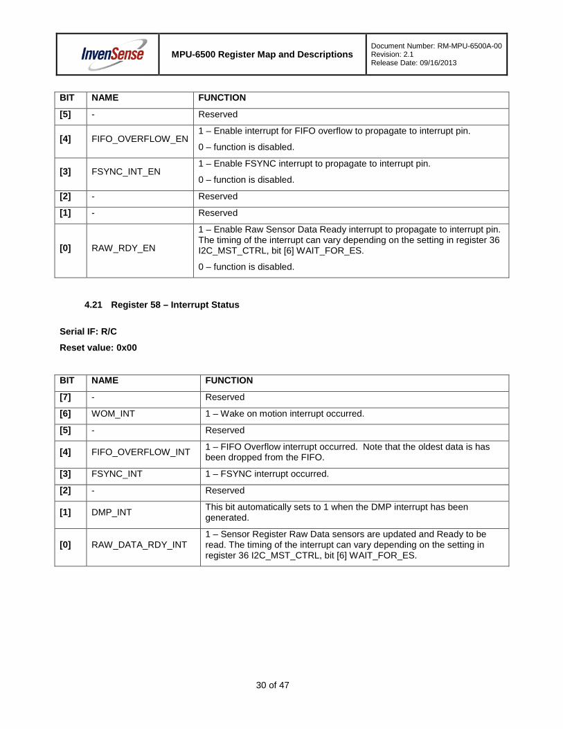
[5] - Reserved
[4] FIFO_OVERFLOW_EN 1 – Enable interrupt for FIFO overflow to propagate to interrupt pin. 0 – function is disabled.
[3] FSYNC_INT_EN 1 – Enable FSYNC interrupt to propagate to interrupt pin. 0 – function is disabled.
[2] - Reserved
[1] - Reserved
[0] RAW_RDY_EN
1 – Enable Raw Sensor Data Ready interrupt to propagate to interrupt pin. The timing of the interrupt can vary depending on the setting in register 36 I2C_MST_CTRL, bit [6] WAIT_FOR_ES. 0 – function is disabled.
4.21 Register 58 – Interrupt Status
Serial IF: R/C
Reset value: 0x00
BIT NAME FUNCTION
[7] - Reserved
[6] WOM_INT 1 – Wake on motion interrupt occurred.
[5] - Reserved
[4] FIFO_OVERFLOW_INT 1 – FIFO Overflow interrupt occurred. Note that the oldest data is has been dropped from the FIFO.
[3] FSYNC_INT 1 – FSYNC interrupt occurred.
[2] - Reserved
[1] DMP_INT This bit automatically sets to 1 when the DMP interrupt has been generated.
[0] RAW_DATA_RDY_INT 1 – Sensor Register Raw Data sensors are updated and Ready to be read. The timing of the interrupt can vary depending on the setting in register 36 I2C_MST_CTRL, bit [6] WAIT_FOR_ES.
30 of 47
MPU-6500 Register Map and Descriptions
Document Number: RM-MPU-6500A-00 Revision: 2.1 Release Date: 09/16/2013
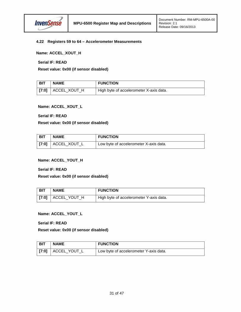
4.22 Registers 59 to 64 – Accelerometer Measurements
Name: ACCEL_XOUT_H
Serial IF: READ
Reset value: 0x00 (if sensor disabled)
BIT NAME FUNCTION
[7:0] ACCEL_XOUT_H High byte of accelerometer X-axis data.
Name: ACCEL_XOUT_L
Serial IF: READ
Reset value: 0x00 (if sensor disabled)
BIT NAME FUNCTION
[7:0] ACCEL_XOUT_L Low byte of accelerometer X-axis data.
Name: ACCEL_YOUT_H
Serial IF: READ
Reset value: 0x00 (if sensor disabled)
BIT NAME FUNCTION
[7:0] ACCEL_YOUT_H High byte of accelerometer Y-axis data.
Name: ACCEL_YOUT_L
Serial IF: READ
Reset value: 0x00 (if sensor disabled)
BIT NAME FUNCTION
[7:0] ACCEL_YOUT_L Low byte of accelerometer Y-axis data.
31 of 47
MPU-6500 Register Map and Descriptions
Document Number: RM-MPU-6500A-00 Revision: 2.1 Release Date: 09/16/2013
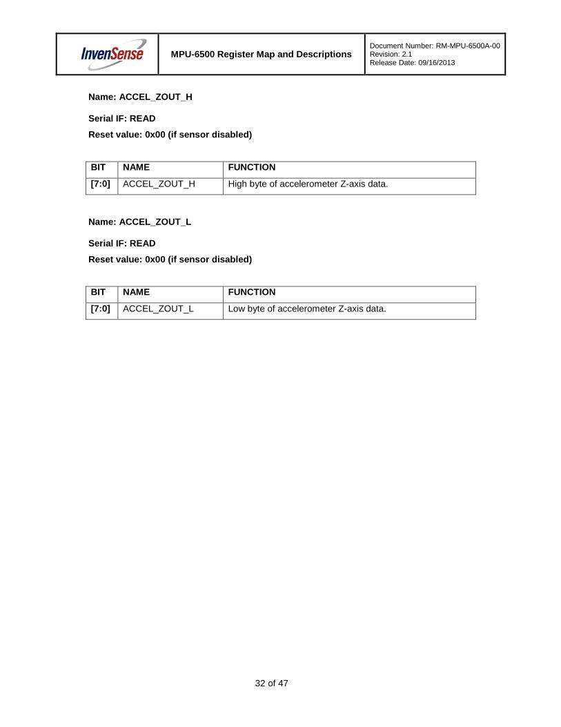
Name: ACCEL_ZOUT_H
Serial IF: READ
Reset value: 0x00 (if sensor disabled)
BIT NAME FUNCTION
[7:0] ACCEL_ZOUT_H High byte of accelerometer Z-axis data.
Name: ACCEL_ZOUT_L
Serial IF: READ
Reset value: 0x00 (if sensor disabled)
BIT NAME FUNCTION
[7:0] ACCEL_ZOUT_L Low byte of accelerometer Z-axis data.
32 of 47
MPU-6500 Register Map and Descriptions
Document Number: RM-MPU-6500A-00 Revision: 2.1 Release Date: 09/16/2013
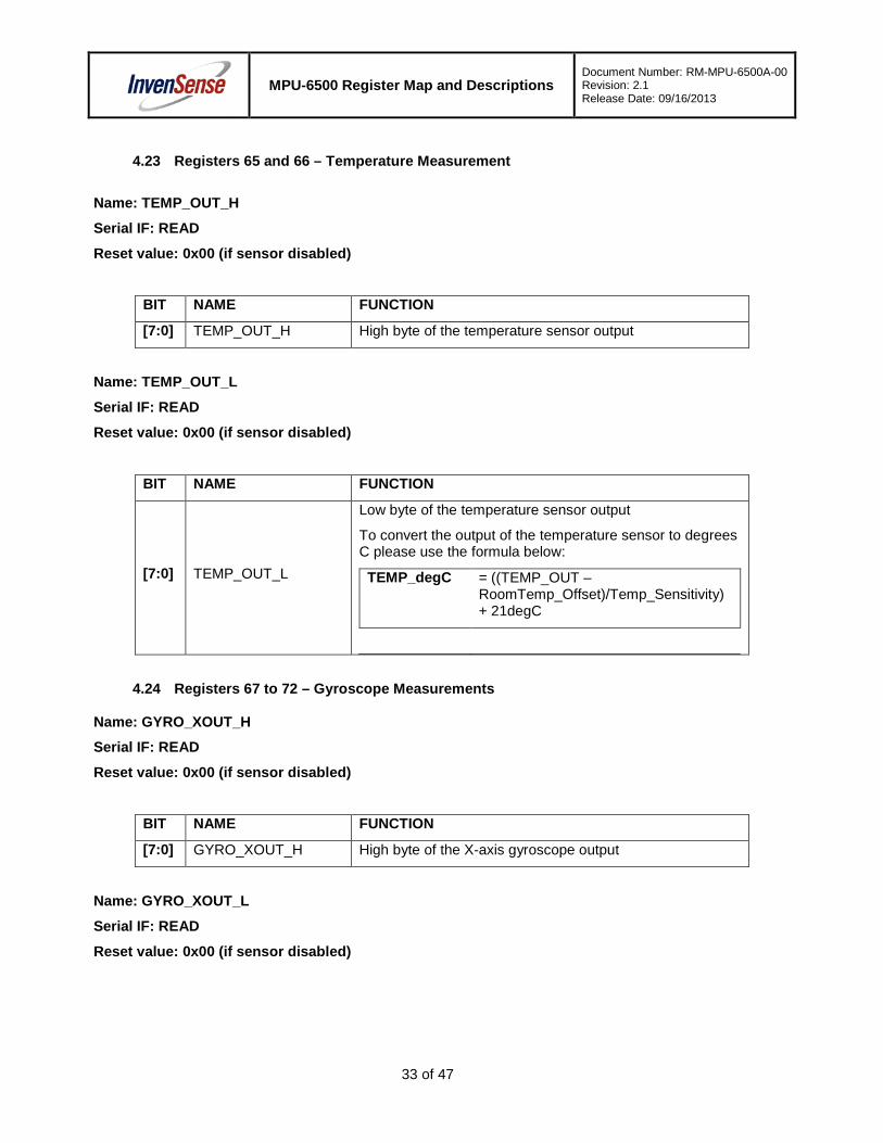
4.23 Registers 65 and 66 – Temperature Measurement
Name: TEMP_OUT_H
Serial IF: READ
Reset value: 0x00 (if sensor disabled)
BIT NAME FUNCTION
[7:0] TEMP_OUT_H High byte of the temperature sensor output
Name: TEMP_OUT_L
Serial IF: READ
Reset value: 0x00 (if sensor disabled)
BIT NAME FUNCTION
[7:0] TEMP_OUT_L
Low byte of the temperature sensor output
To convert the output of the temperature sensor to degrees C please use the formula below:
TEMP_degC = ((TEMP_OUT – RoomTemp_Offset)/Temp_Sensitivity) + 21degC
4.24 Registers 67 to 72 – Gyroscope Measurements Name: GYRO_XOUT_H
Serial IF: READ
Reset value: 0x00 (if sensor disabled)
BIT NAME FUNCTION
[7:0] GYRO_XOUT_H High byte of the X-axis gyroscope output
Name: GYRO_XOUT_L
Serial IF: READ
Reset value: 0x00 (if sensor disabled)
33 of 47
MPU-6500 Register Map and Descriptions
Document Number: RM-MPU-6500A-00 Revision: 2.1 Release Date: 09/16/2013
BIT NAME FUNCTION
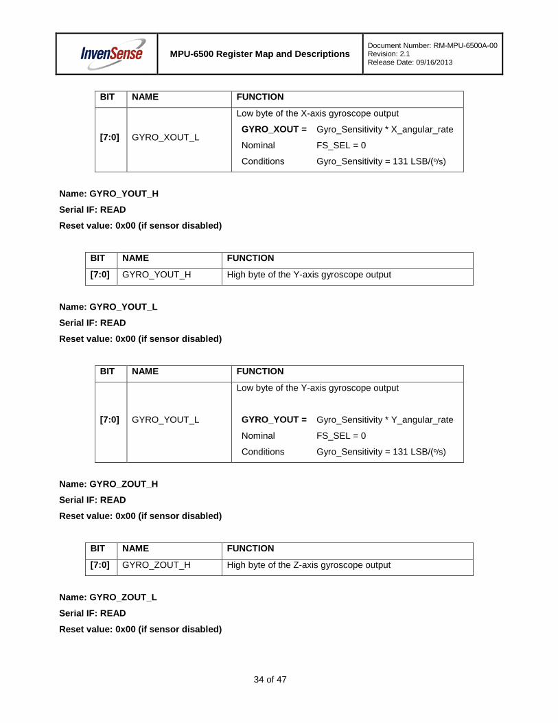
[7:0] GYRO_XOUT_L
Low byte of the X-axis gyroscope output GYRO_XOUT = Gyro_Sensitivity * X_angular_rate
Nominal
Conditions
FS_SEL = 0 Gyro_Sensitivity = 131 LSB/(º/s)
Name: GYRO_YOUT_H
Serial IF: READ
Reset value: 0x00 (if sensor disabled)
BIT NAME FUNCTION
[7:0] GYRO_YOUT_H High byte of the Y-axis gyroscope output
Name: GYRO_YOUT_L
Serial IF: READ
Reset value: 0x00 (if sensor disabled)
BIT NAME FUNCTION
[7:0] GYRO_YOUT_L
Low byte of the Y-axis gyroscope output
GYRO_YOUT = Gyro_Sensitivity * Y_angular_rate
Nominal
Conditions
FS_SEL = 0 Gyro_Sensitivity = 131 LSB/(º/s)
Name: GYRO_ZOUT_H
Serial IF: READ
Reset value: 0x00 (if sensor disabled)
BIT NAME FUNCTION
[7:0] GYRO_ZOUT_H High byte of the Z-axis gyroscope output
Name: GYRO_ZOUT_L
Serial IF: READ
Reset value: 0x00 (if sensor disabled)
34 of 47
MPU-6500 Register Map and Descriptions
Document Number: RM-MPU-6500A-00 Revision: 2.1 Release Date: 09/16/2013
BIT NAME FUNCTION
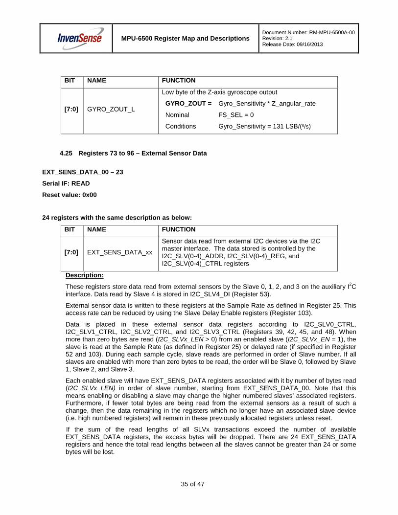
[7:0] GYRO_ZOUT_L
Low byte of the Z-axis gyroscope output GYRO_ZOUT = Gyro_Sensitivity * Z_angular_rate
Nominal
Conditions
FS_SEL = 0 Gyro_Sensitivity = 131 LSB/(º/s)
4.25 Registers 73 to 96 – External Sensor Data
EXT_SENS_DATA_00 – 23
Serial IF: READ
Reset value: 0x00
24 registers with the same description as below:
BIT NAME FUNCTION
[7:0] EXT_SENS_DATA_xx Sensor data read from external I2C devices via the I2C master interface. The data stored is controlled by the I2C_SLV(0-4)_ADDR, I2C_SLV(0-4)_REG, and I2C_SLV(0-4)_CTRL registers
Description:
These registers store data read from external sensors by the Slave 0, 1, 2, and 3 on the auxiliary I2C interface. Data read by Slave 4 is stored in I2C_SLV4_DI (Register 53).
External sensor data is written to these registers at the Sample Rate as defined in Register 25. This access rate can be reduced by using the Slave Delay Enable registers (Register 103).
Data is placed in these external sensor data registers according to I2C_SLV0_CTRL, I2C_SLV1_CTRL, I2C_SLV2_CTRL, and I2C_SLV3_CTRL (Registers 39, 42, 45, and 48). When more than zero bytes are read (I2C_SLVx_LEN > 0) from an enabled slave (I2C_SLVx_EN = 1), the slave is read at the Sample Rate (as defined in Register 25) or delayed rate (if specified in Register 52 and 103). During each sample cycle, slave reads are performed in order of Slave number. If all slaves are enabled with more than zero bytes to be read, the order will be Slave 0, followed by Slave 1, Slave 2, and Slave 3.
Each enabled slave will have EXT_SENS_DATA registers associated with it by number of bytes read (I2C_SLVx_LEN) in order of slave number, starting from EXT_SENS_DATA_00. Note that this means enabling or disabling a slave may change the higher numbered slaves’ associated registers. Furthermore, if fewer total bytes are being read from the external sensors as a result of such a change, then the data remaining in the registers which no longer have an associated slave device (i.e. high numbered registers) will remain in these previously allocated registers unless reset.
If the sum of the read lengths of all SLVx transactions exceed the number of available EXT_SENS_DATA registers, the excess bytes will be dropped. There are 24 EXT_SENS_DATA registers and hence the total read lengths between all the slaves cannot be greater than 24 or some bytes will be lost.
35 of 47
MPU-6500 Register Map and Descriptions
Document Number: RM-MPU-6500A-00 Revision: 2.1 Release Date: 09/16/2013
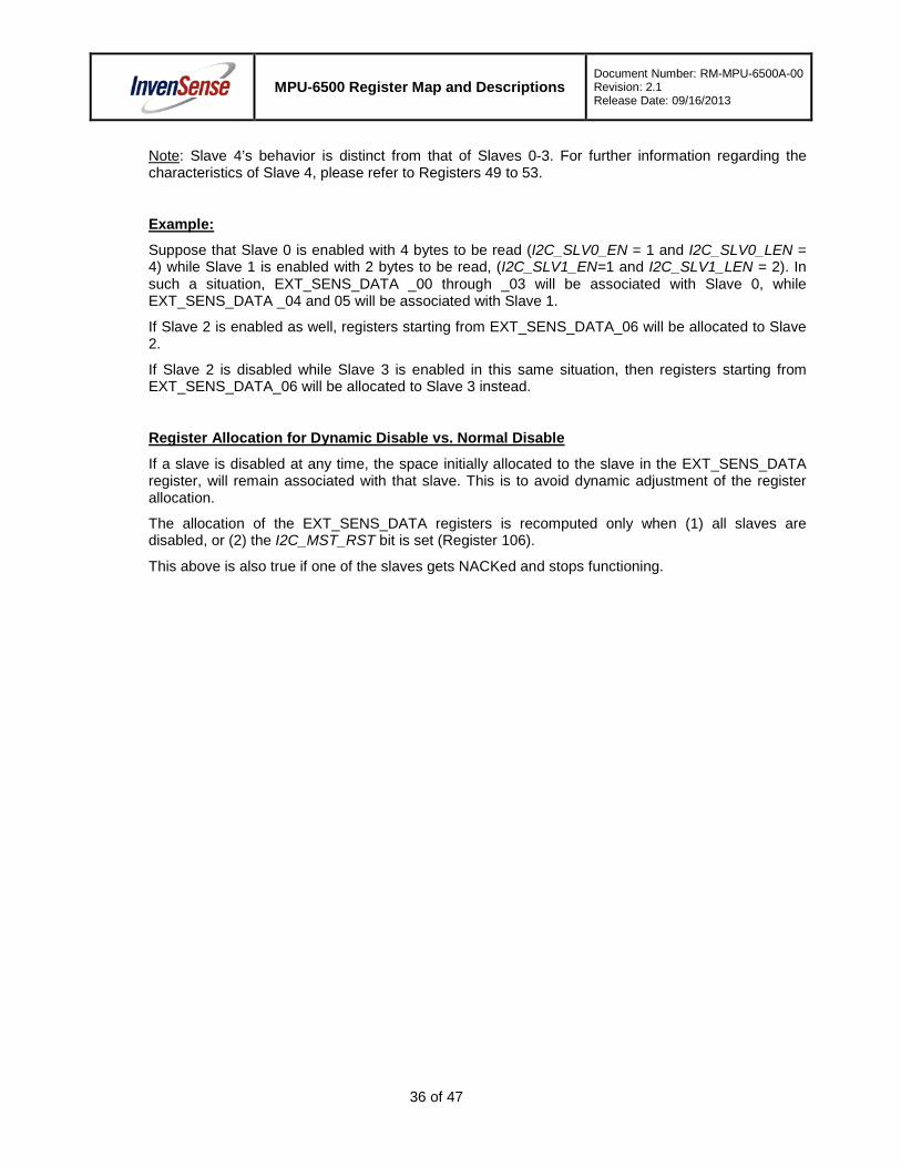
Note: Slave 4’s behavior is distinct from that of Slaves 0-3. For further information regarding the characteristics of Slave 4, please refer to Registers 49 to 53.
Example:
Suppose that Slave 0 is enabled with 4 bytes to be read (I2C_SLV0_EN = 1 and I2C_SLV0_LEN = 4) while Slave 1 is enabled with 2 bytes to be read, (I2C_SLV1_EN=1 and I2C_SLV1_LEN = 2). In such a situation, EXT_SENS_DATA _00 through _03 will be associated with Slave 0, while EXT_SENS_DATA _04 and 05 will be associated with Slave 1.
If Slave 2 is enabled as well, registers starting from EXT_SENS_DATA_06 will be allocated to Slave 2.
If Slave 2 is disabled while Slave 3 is enabled in this same situation, then registers starting from EXT_SENS_DATA_06 will be allocated to Slave 3 instead.
Register Allocation for Dynamic Disable vs. Normal Disable
If a slave is disabled at any time, the space initially allocated to the slave in the EXT_SENS_DATA register, will remain associated with that slave. This is to avoid dynamic adjustment of the register allocation.
The allocation of the EXT_SENS_DATA registers is recomputed only when (1) all slaves are disabled, or (2) the I2C_MST_RST bit is set (Register 106).
This above is also true if one of the slaves gets NACKed and stops functioning.
36 of 47
MPU-6500 Register Map and Descriptions
Document Number: RM-MPU-6500A-00 Revision: 2.1 Release Date: 09/16/2013
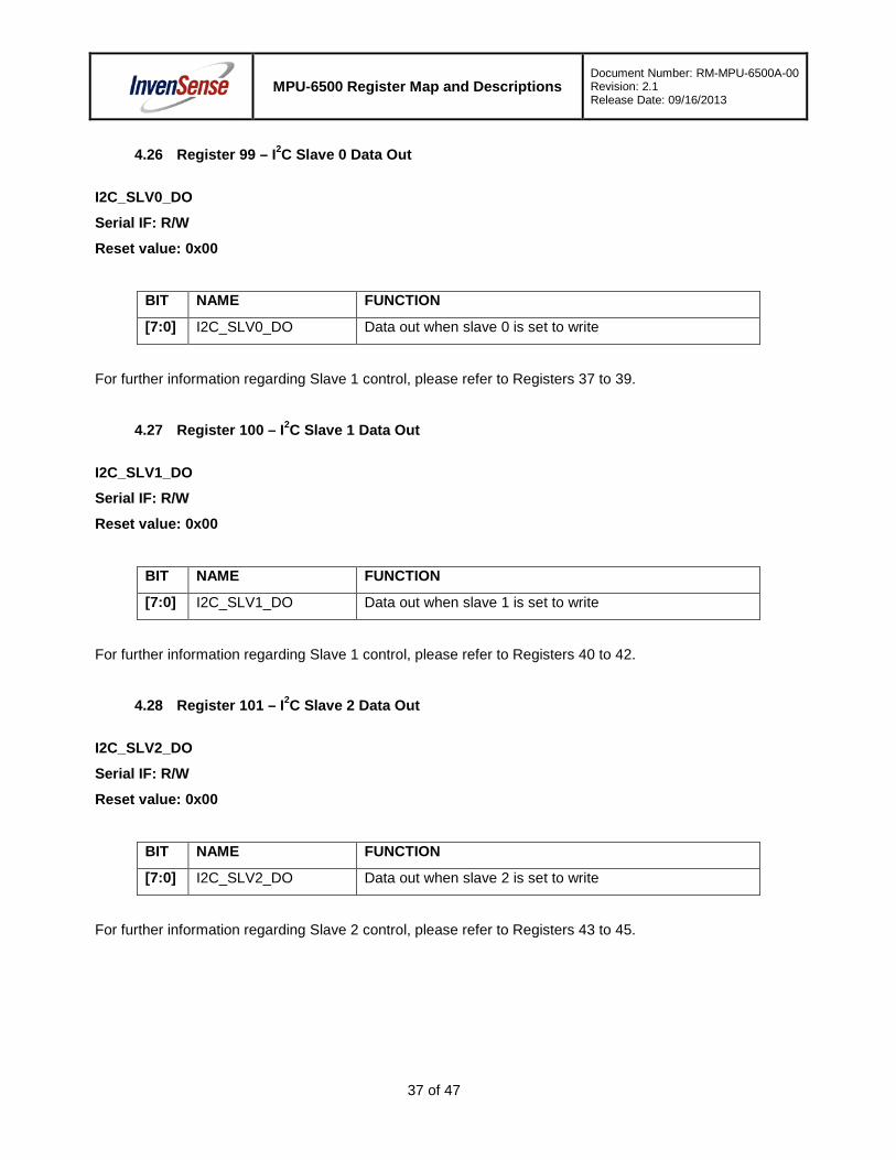
4.26 Register 99 – I2C Slave 0 Data Out
I2C_SLV0_DO
Serial IF: R/W
Reset value: 0x00
BIT NAME FUNCTION
[7:0] I2C_SLV0_DO Data out when slave 0 is set to write
For further information regarding Slave 1 control, please refer to Registers 37 to 39.
4.27 Register 100 – I2C Slave 1 Data Out
I2C_SLV1_DO
Serial IF: R/W
Reset value: 0x00
BIT NAME FUNCTION
[7:0] I2C_SLV1_DO Data out when slave 1 is set to write
For further information regarding Slave 1 control, please refer to Registers 40 to 42.
4.28 Register 101 – I2C Slave 2 Data Out
I2C_SLV2_DO
Serial IF: R/W
Reset value: 0x00
BIT NAME FUNCTION
[7:0] I2C_SLV2_DO Data out when slave 2 is set to write
For further information regarding Slave 2 control, please refer to Registers 43 to 45.
37 of 47
MPU-6500 Register Map and Descriptions
Document Number: RM-MPU-6500A-00 Revision: 2.1 Release Date: 09/16/2013
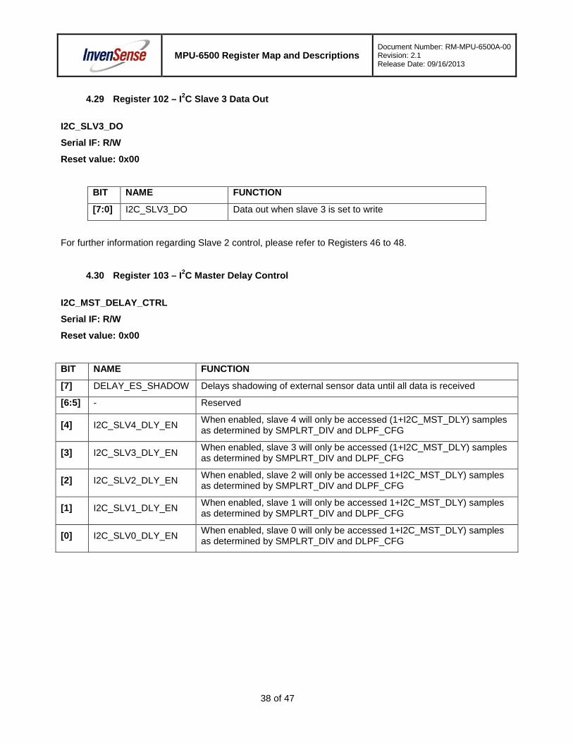
4.29 Register 102 – I2C Slave 3 Data Out
I2C_SLV3_DO
Serial IF: R/W
Reset value: 0x00
BIT NAME FUNCTION
[7:0] I2C_SLV3_DO Data out when slave 3 is set to write
For further information regarding Slave 2 control, please refer to Registers 46 to 48.
4.30 Register 103 – I2C Master Delay Control
I2C_MST_DELAY_CTRL
Serial IF: R/W
Reset value: 0x00
BIT NAME FUNCTION
[7] DELAY_ES_SHADOW Delays shadowing of external sensor data until all data is received [6:5] - Reserved
[4] I2C_SLV4_DLY_EN When enabled, slave 4 will only be accessed (1+I2C_MST_DLY) samples as determined by SMPLRT_DIV and DLPF_CFG
[3] I2C_SLV3_DLY_EN When enabled, slave 3 will only be accessed (1+I2C_MST_DLY) samples as determined by SMPLRT_DIV and DLPF_CFG
[2] I2C_SLV2_DLY_EN When enabled, slave 2 will only be accessed 1+I2C_MST_DLY) samples as determined by SMPLRT_DIV and DLPF_CFG
[1] I2C_SLV1_DLY_EN When enabled, slave 1 will only be accessed 1+I2C_MST_DLY) samples as determined by SMPLRT_DIV and DLPF_CFG
[0] I2C_SLV0_DLY_EN When enabled, slave 0 will only be accessed 1+I2C_MST_DLY) samples as determined by SMPLRT_DIV and DLPF_CFG
38 of 47
MPU-6500 Register Map and Descriptions
Document Number: RM-MPU-6500A-00 Revision: 2.1 Release Date: 09/16/2013
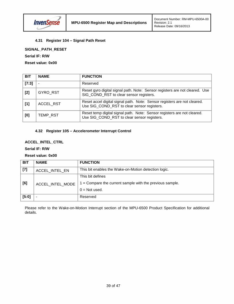
4.31 Register 104 – Signal Path Reset SIGNAL_PATH_RESET
Serial IF: R/W
Reset value: 0x00
BIT NAME FUNCTION
[7:3] - Reserved
[2] GYRO_RST Reset gyro digital signal path. Note: Sensor registers are not cleared. Use SIG_COND_RST to clear sensor registers.
[1] ACCEL_RST Reset accel digital signal path. Note: Sensor registers are not cleared. Use SIG_COND_RST to clear sensor registers.
[0] TEMP_RST Reset temp digital signal path. Note: Sensor registers are not cleared. Use SIG_COND_RST to clear sensor registers.
4.32 Register 105 – Accelerometer Interrupt Control
ACCEL_INTEL_CTRL
Serial IF: R/W
Reset value: 0x00
BIT NAME FUNCTION
[7] ACCEL_INTEL_EN This bit enables the Wake-on-Motion detection logic.
[6] ACCEL_INTEL_MODE
This bit defines
1 = Compare the current sample with the previous sample. 0 = Not used.
[5:0] - Reserved
Please refer to the Wake-on-Motion Interrupt section of the MPU-6500 Product Specification for additional details.
39 of 47
MPU-6500 Register Map and Descriptions
Document Number: RM-MPU-6500A-00 Revision: 2.1 Release Date: 09/16/2013
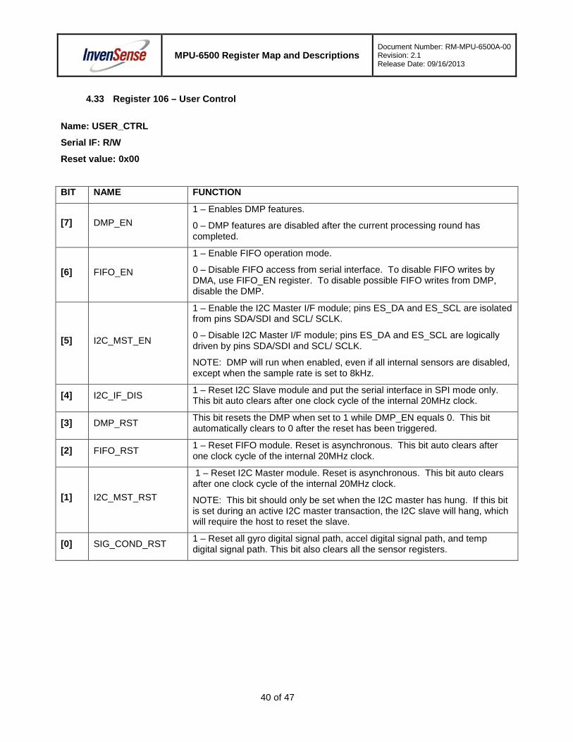
4.33 Register 106 – User Control
Name: USER_CTRL
Serial IF: R/W
Reset value: 0x00
BIT NAME FUNCTION
[7] DMP_EN 1 – Enables DMP features.
0 – DMP features are disabled after the current processing round has completed.
[6] FIFO_EN
1 – Enable FIFO operation mode. 0 – Disable FIFO access from serial interface. To disable FIFO writes by DMA, use FIFO_EN register. To disable possible FIFO writes from DMP, disable the DMP.
[5] I2C_MST_EN
1 – Enable the I2C Master I/F module; pins ES_DA and ES_SCL are isolated from pins SDA/SDI and SCL/ SCLK. 0 – Disable I2C Master I/F module; pins ES_DA and ES_SCL are logically driven by pins SDA/SDI and SCL/ SCLK.
NOTE: DMP will run when enabled, even if all internal sensors are disabled, except when the sample rate is set to 8kHz.
[4] I2C_IF_DIS 1 – Reset I2C Slave module and put the serial interface in SPI mode only. This bit auto clears after one clock cycle of the internal 20MHz clock.
[3] DMP_RST This bit resets the DMP when set to 1 while DMP_EN equals 0. This bit automatically clears to 0 after the reset has been triggered.
[2] FIFO_RST 1 – Reset FIFO module. Reset is asynchronous. This bit auto clears after one clock cycle of the internal 20MHz clock.
[1] I2C_MST_RST
1 – Reset I2C Master module. Reset is asynchronous. This bit auto clears after one clock cycle of the internal 20MHz clock.
NOTE: This bit should only be set when the I2C master has hung. If this bit is set during an active I2C master transaction, the I2C slave will hang, which will require the host to reset the slave.
[0] SIG_COND_RST 1 – Reset all gyro digital signal path, accel digital signal path, and temp digital signal path. This bit also clears all the sensor registers.
40 of 47
MPU-6500 Register Map and Descriptions
Document Number: RM-MPU-6500A-00 Revision: 2.1 Release Date: 09/16/2013
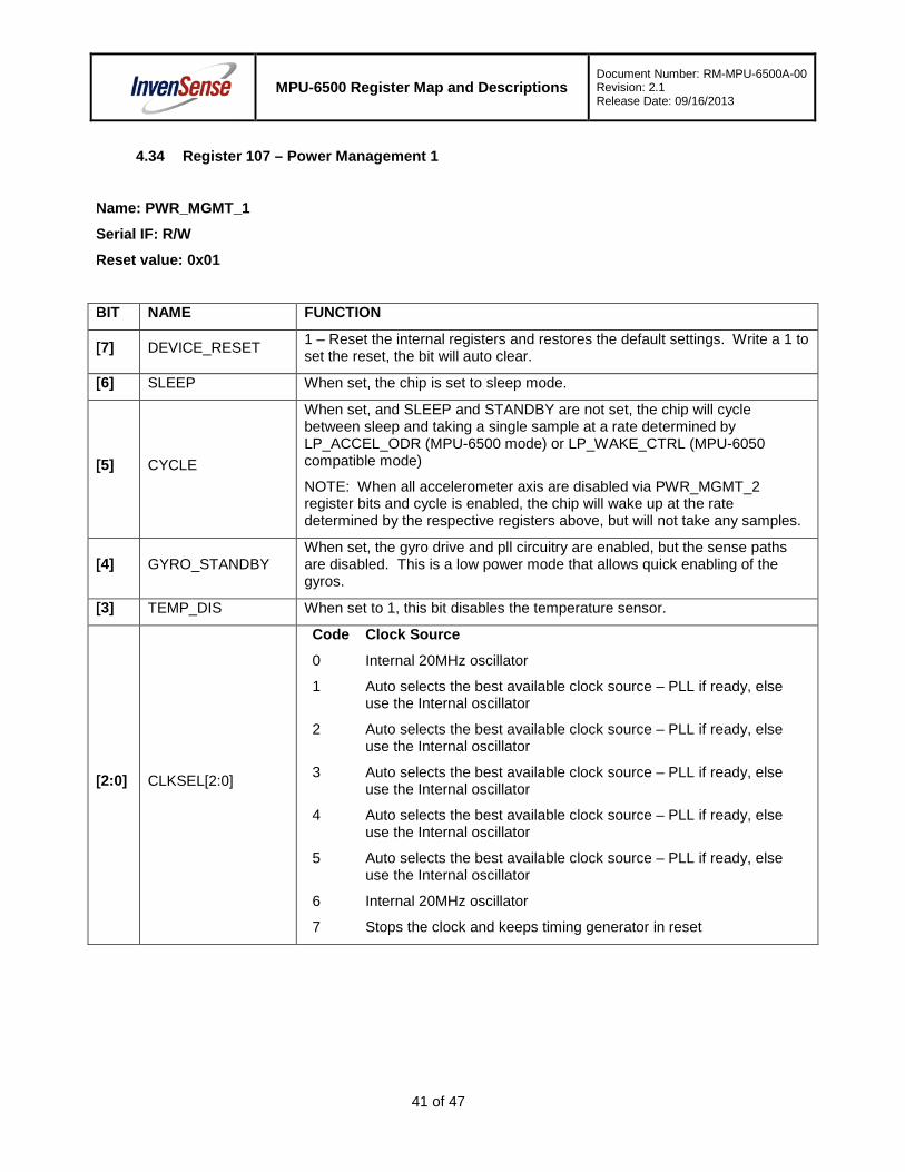
4.34 Register 107 – Power Management 1
Name: PWR_MGMT_1
Serial IF: R/W
Reset value: 0x01
BIT NAME FUNCTION
[7] DEVICE_RESET 1 – Reset the internal registers and restores the default settings. Write a 1 to set the reset, the bit will auto clear.
[6] SLEEP When set, the chip is set to sleep mode.
[5] CYCLE
When set, and SLEEP and STANDBY are not set, the chip will cycle between sleep and taking a single sample at a rate determined by LP_ACCEL_ODR (MPU-6500 mode) or LP_WAKE_CTRL (MPU-6050 compatible mode) NOTE: When all accelerometer axis are disabled via PWR_MGMT_2 register bits and cycle is enabled, the chip will wake up at the rate determined by the respective registers above, but will not take any samples.
[4] GYRO_STANDBY When set, the gyro drive and pll circuitry are enabled, but the sense paths are disabled. This is a low power mode that allows quick enabling of the gyros.
[3] TEMP_DIS When set to 1, this bit disables the temperature sensor.
[2:0] CLKSEL[2:0]
Code Clock Source
0 Internal 20MHz oscillator 1 Auto selects the best available clock source – PLL if ready, else
use the Internal oscillator 2 Auto selects the best available clock source – PLL if ready, else
use the Internal oscillator 3 Auto selects the best available clock source – PLL if ready, else
use the Internal oscillator 4 Auto selects the best available clock source – PLL if ready, else
use the Internal oscillator 5 Auto selects the best available clock source – PLL if ready, else
use the Internal oscillator 6 Internal 20MHz oscillator 7 Stops the clock and keeps timing generator in reset
41 of 47
MPU-6500 Register Map and Descriptions
Document Number: RM-MPU-6500A-00 Revision: 2.1 Release Date: 09/16/2013
Note:
When using SPI interface, user should use PWR_MGMT_1 (register 107) as well as SIGNAL_PATH_RESET (register 104) to ensure the reset is performed properly. The sequence used should be:
1. Set H_RESET = 1 (register PWR_MGMT_1) 2. Wait 100ms 3. Set GYRO_RST = ACCEL_RST = TEMP_RST = 1 (register SIGNAL_PATH_RESET) 4. Wait 100ms
4.35 Register 108 – Power Management 2
Name: PWR_MGMT_2
Serial IF: R/W
Reset value: 0x00
BIT NAME FUNCTION
[7:6] LP_WAKE_CTRL[1:0] Specifies the frequency of wake-ups during Accelerometer Only Low Power Mode.
[5] DISABLE_XA 1 – X accelerometer is disabled 0 – X accelerometer is on
[4] DISABLE_YA 1 – Y accelerometer is disabled 0 – Y accelerometer is on
[3] DISABLE_ZA 1 – Z accelerometer is disabled 0 – Z accelerometer is on
[2] DISABLE_XG 1 – X gyro is disabled 0 – X gyro is on
[1] DISABLE_YG 1 – Y gyro is disabled 0 – Y gyro is on
[0] DISABLE_ZG 1 – Z gyro is disabled 0 – Z gyro is on
MPU-6050 compatible mode:
In addition to the above default MPU-6500 mode, this register allows the user to configure the frequency of wake-ups in Accelerometer Only Low Power Mode using the LP_WAKE_CTRL bits.
The MPU-6500 can be put into Accelerometer Only Low Power Mode using the following steps:
(i) Set CYCLE bit to 1 (ii) Set SLEEP bit to 0 (iii) Set TEMP_DIS bit to 1
42 of 47
MPU-6500 Register Map and Descriptions
Document Number: RM-MPU-6500A-00 Revision: 2.1 Release Date: 09/16/2013
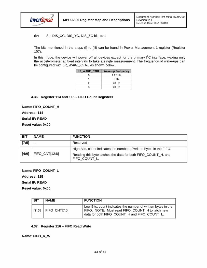
(iv) Set DIS_XG, DIS_YG, DIS_ZG bits to 1
The bits mentioned in the steps (i) to (iii) can be found in Power Management 1 register (Register 107).
In this mode, the device will power off all devices except for the primary I2C interface, waking only the accelerometer at fixed intervals to take a single measurement. The frequency of wake-ups can be configured with LP_WAKE_CTRL as shown below.
LP_WAKE_CTRL Wake-up Frequency 0 1.25 Hz 1 5 Hz 2 20 Hz 3 40 Hz
4.36 Register 114 and 115 – FIFO Count Registers
Name: FIFO_COUNT_H
Address: 114
Serial IF: READ
Reset value: 0x00
BIT NAME FUNCTION
[7:5] - Reserved
[4:0] FIFO_CNT[12:8] High Bits, count indicates the number of written bytes in the FIFO. Reading this byte latches the data for both FIFO_COUNT_H, and FIFO_COUNT_L.
Name: FIFO_COUNT_L
Address: 115
Serial IF: READ
Reset value: 0x00
BIT NAME FUNCTION
[7:0] FIFO_CNT[7:0] Low Bits, count indicates the number of written bytes in the FIFO. NOTE: Must read FIFO_COUNT_H to latch new data for both FIFO_COUNT_H and FIFO_COUNT_L.
4.37 Register 116 – FIFO Read Write
Name: FIFO_R_W
43 of 47
MPU-6500 Register Map and Descriptions
Document Number: RM-MPU-6500A-00 Revision: 2.1 Release Date: 09/16/2013
Serial IF: READ
Reset value: 0x00
BIT NAME FUNCTION
[7:0] D[7:0] Read/Write command provides Read or Write operation for the FIFO.
Description:
This register is used to read and write data from the FIFO buffer.
Data is written to the FIFO in order of register number (from lowest to highest). If all the FIFO enable flags (see below) are enabled and all External Sensor Data registers (Registers 73 to 96) are associated with a Slave device, the contents of registers 59 through 96 will be written in order at the Sample Rate.
The contents of the sensor data registers (Registers 59 to 96) are written into the FIFO buffer when their corresponding FIFO enable flags are set to 1 in FIFO_EN (Register 35). An additional flag for the sensor data registers associated with I2C Slave 3 can be found in I2C_MST_CTRL (Register 36).
If the FIFO buffer has overflowed, the status bit FIFO_OFLOW_INT is automatically set to 1. This bit is located in INT_STATUS (Register 58). When the FIFO buffer has overflowed, the oldest data will be lost and new data will be written to the FIFO unless register 26 CONFIG, bit[6] FIFO_MODE = 1.
If the FIFO buffer is empty, reading this register will return the last byte that was previously read from the FIFO until new data is available. The user should check FIFO_COUNT to ensure that the FIFO buffer is not read when empty.
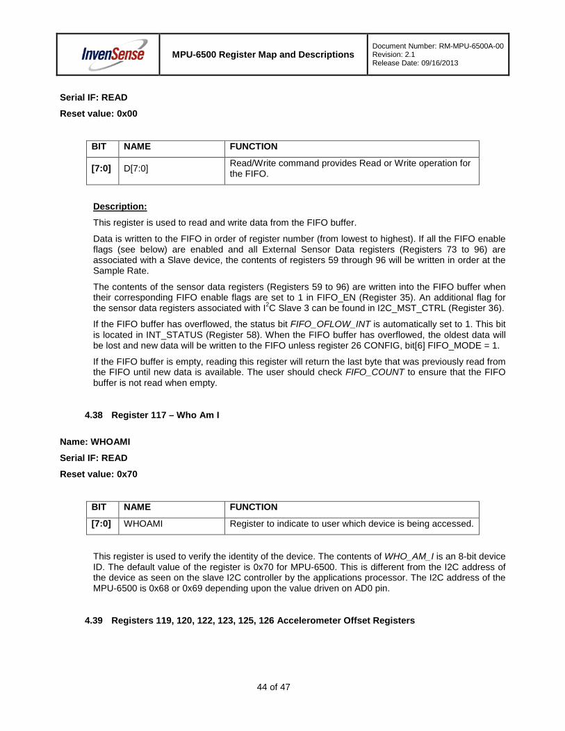
4.38 Register 117 – Who Am I
Name: WHOAMI
Serial IF: READ
Reset value: 0x70
BIT NAME FUNCTION
[7:0] WHOAMI Register to indicate to user which device is being accessed.
This register is used to verify the identity of the device. The contents of WHO_AM_I is an 8-bit device ID. The default value of the register is 0x70 for MPU-6500. This is different from the I2C address of the device as seen on the slave I2C controller by the applications processor. The I2C address of the MPU-6500 is 0x68 or 0x69 depending upon the value driven on AD0 pin.
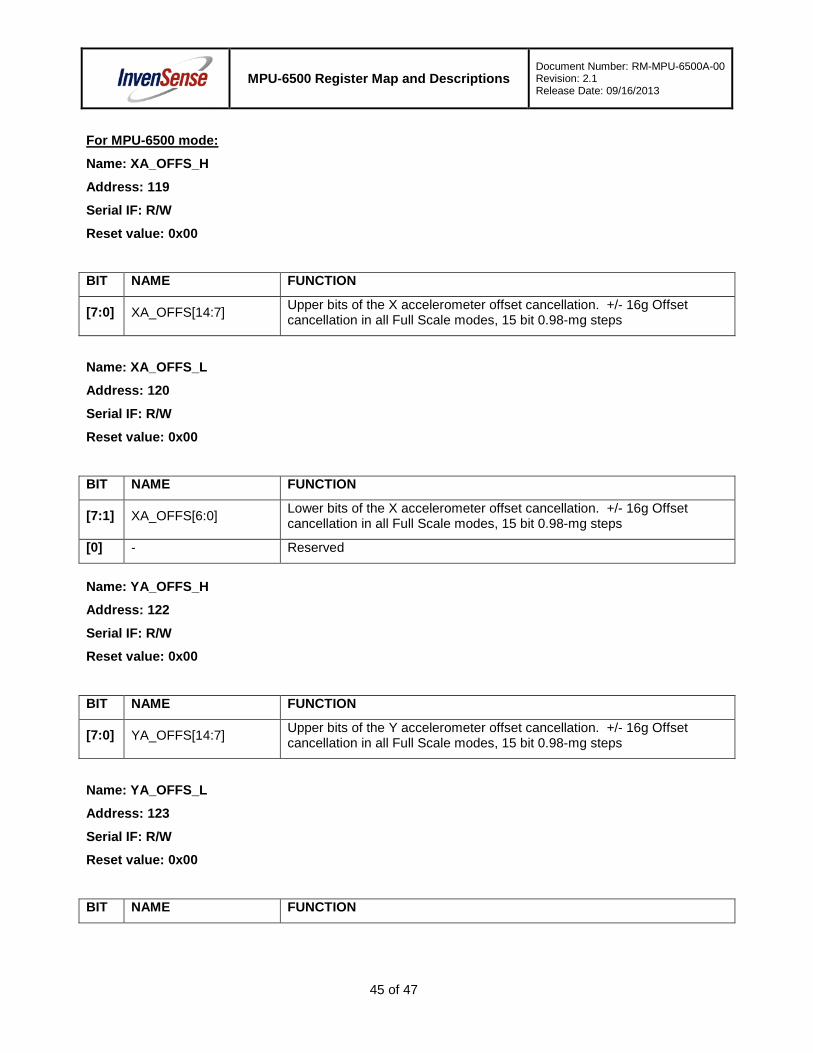
4.39 Registers 119, 120, 122, 123, 125, 126 Accelerometer Offset Registers
44 of 47
MPU-6500 Register Map and Descriptions
Document Number: RM-MPU-6500A-00 Revision: 2.1 Release Date: 09/16/2013
For MPU-6500 mode:
Name: XA_OFFS_H
Address: 119
Serial IF: R/W
Reset value: 0x00
BIT NAME FUNCTION
[7:0] XA_OFFS[14:7] Upper bits of the X accelerometer offset cancellation. +/- 16g Offset cancellation in all Full Scale modes, 15 bit 0.98-mg steps
Name: XA_OFFS_L
Address: 120
Serial IF: R/W
Reset value: 0x00
BIT NAME FUNCTION
[7:1] XA_OFFS[6:0] Lower bits of the X accelerometer offset cancellation. +/- 16g Offset cancellation in all Full Scale modes, 15 bit 0.98-mg steps
[0] - Reserved
Name: YA_OFFS_H
Address: 122
Serial IF: R/W
Reset value: 0x00
BIT NAME FUNCTION
[7:0] YA_OFFS[14:7] Upper bits of the Y accelerometer offset cancellation. +/- 16g Offset cancellation in all Full Scale modes, 15 bit 0.98-mg steps
Name: YA_OFFS_L
Address: 123
Serial IF: R/W
Reset value: 0x00
BIT NAME FUNCTION
45 of 47
MPU-6500 Register Map and Descriptions
Document Number: RM-MPU-6500A-00 Revision: 2.1 Release Date: 09/16/2013
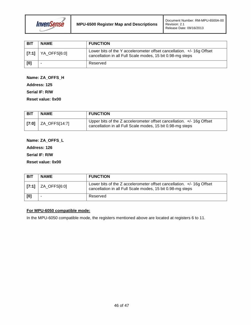
BIT NAME FUNCTION
[7:1] YA_OFFS[6:0] Lower bits of the Y accelerometer offset cancellation. +/- 16g Offset cancellation in all Full Scale modes, 15 bit 0.98-mg steps
[0] - Reserved
Name: ZA_OFFS_H
Address: 125
Serial IF: R/W
Reset value: 0x00
BIT NAME FUNCTION
[7:0] ZA_OFFS[14:7] Upper bits of the Z accelerometer offset cancellation. +/- 16g Offset cancellation in all Full Scale modes, 15 bit 0.98-mg steps
Name: ZA_OFFS_L
Address: 126
Serial IF: R/W
Reset value: 0x00
BIT NAME FUNCTION
[7:1] ZA_OFFS[6:0] Lower bits of the Z accelerometer offset cancellation. +/- 16g Offset cancellation in all Full Scale modes, 15 bit 0.98-mg steps
[0] - Reserved
For MPU-6050 compatible mode:
In the MPU-6050 compatible mode, the registers mentioned above are located at registers 6 to 11.
46 of 47
MPU-6500 Register Map and Descriptions
Document Number: RM-MPU-6500A-00 Revision: 2.1 Release Date: 09/16/2013
This information furnished by InvenSense is believed to be accurate and reliable. However, no responsibility is assumed by InvenSense for its use, or for any infringements of patents or other rights of third parties that may result from its use. Specifications are subject to change without notice. InvenSense reserves the right to make changes to this product, including its circuits and software, in order to improve its design and/or performance, without prior notice. InvenSense makes no warranties, neither expressed nor implied, regarding the information and specifications contained in this document. InvenSense assumes no responsibility for any claims or damages arising from information contained in this document, or from the use of products and services detailed therein. This includes, but is not limited to, claims or damages based on the infringement of patents, copyrights, mask work and/or other intellectual property rights.
Certain intellectual property owned by InvenSense and described in this document is patent protected. No license is granted by implication or otherwise under any patent or patent rights of InvenSense. This publication supersedes and replaces all information previously supplied. Trademarks that are registered trademarks are the property of their respective companies. InvenSense sensors should not be used or sold in the development, storage, production or utilization of any conventional or mass-destructive weapons or for any other weapons or life threatening applications, as well as in any other life critical applications such as medical equipment, transportation, aerospace and nuclear instruments, undersea equipment, power plant equipment, disaster prevention and crime prevention equipment.
InvenSense® is a registered trademark of InvenSense, Inc. MPUTM, MPU-6500TM, Digital Motion Processor™, DMP ™, MPU-6000TM, and MPU-6050TM are trademarks of InvenSense, Inc.
©2013 InvenSense, Inc. All rights reserved.
47 of 47