msc1200: precision adc and dac with 8051 …media.digikey.com/pdf/data sheets/texas instruments...
TRANSCRIPT

MSC1200
MSC1200
SBAS289C – JUNE 2003 – REVISED JUNE 2004
www.ti.com
Copyright © 2003-2004, Texas Instruments Incorporated
Please be aware that an important notice concerning availability, standard warranty, and use in critical applications ofTexas Instruments semiconductor products and disclaimers thereto appears at the end of this data sheet.
All trademarks are the property of their respective owners.
Precision Analog-to-Digital Converter (ADC)and Digital-to-Analog Converter (DAC)
with 8051 Microcontroller and Flash Memory
FEATURESANALOG FEATURES
24-BITS NO MISSING CODES 22-BITS EFFECTIVE RESOLUTION AT 10Hz
Low Noise: 75nV PGA FROM 1 TO 128 PRECISION ON-CHIP VOLTAGE REFERENCE 8 DIFFERENTIAL/SINGLE-ENDED CHANNELS ON-CHIP OFFSET/GAIN CALIBRATION OFFSET DRIFT: 0.02ppm/°C GAIN DRIFT: 0.5ppm/°C ON-CHIP TEMPERATURE SENSOR SELECTABLE BUFFER INPUT BURNOUT DETECT 8-BIT CURRENT DAC
DIGITAL FEATURES
Microcontroller Core
8051-COMPATIBLE HIGH-SPEED CORE:
4 Clocks per Instruction Cycle DC TO 33MHz ON-CHIP OSCILLATOR PLL WITH 32kHz CAPABILITY SINGLE INSTRUCTION 121ns DUAL DATA POINTER
Memory
4kB OR 8kB OF FLASH MEMORY FLASH MEMORY PARTITIONING ENDURANCE 1M ERASE/WRITE CYCLES,
100 YEAR DATA RETENTION 128 BYTES DATA SRAM IN-SYSTEM SERIALLY PROGRAMMABLE FLASH MEMORY SECURITY 1kB BOOT ROM
Peripheral Features
16 DIGITAL I/O PINS ADDITIONAL 32-BIT ACCUMULATOR TWO 16-BIT TIMER/COUNTERS SYSTEM TIMERS PROGRAMMABLE WATCHDOG TIMER FULL DUPLEX UART BASIC SPI™
BASIC I2C™
POWER MANAGEMENT CONTROL INTERNAL CLOCK DIVIDER IDLE MODE CURRENT < 200µA STOP MODE CURRENT < 100nA DIGITAL BROWNOUT RESET ANALOG LOW VOLTAGE DETECT 20 INTERRUPT SOURCES
GENERAL FEATURES
PACKAGE: TQFP-48 LOW POWER: 3mW INDUSTRIAL TEMPERATURE RANGE:
–40°C to +85°C POWER SUPPLY: 2.7V to 5.25V
APPLICATIONS INDUSTRIAL PROCESS CONTROL INSTRUMENTATION LIQUID/GAS CHROMATOGRAPHY BLOOD ANALYSIS SMART TRANSMITTERS PORTABLE INSTRUMENTS WEIGH SCALES PRESSURE TRANSDUCERS INTELLIGENT SENSORS PORTABLE APPLICATIONS DAS SYSTEMS
PRODUCTION DATA information is current as of publication date.Products conform to specifications per the terms of Texas Instrumentsstandard warranty. Production processing does not necessarily includetesting of all parameters.

MSC12002SBAS289Cwww.ti.com
PACKAGE/ORDERING INFORMATIONSPECIFIED
FLASH PACKAGE TEMPERATURE PACKAGE ORDERING TRANSPORTPRODUCT MEMORY PACKAGE-LEAD DESIGNATOR(1) RANGE MARKING NUMBER MEDIA, QUANTITY
MSC1200Y2 4k TQFP-48 PFB –40°C to +85°C MSC1200Y2 MSC1200Y2PFBT Tape and Reel, 250MSC1200Y2 4k " " " " MSC1200Y2PFBR Tape and Reel, 2000
MSC1200Y3 8k TQFP-48 PFB –40°C to +85°C MSC1200Y3 MSC1200Y3PFBT Tape and Reel, 250MSC1200Y3 8k " " " " MSC1200Y3PFBR Tape and Reel, 2000
NOTE: (1) For the most current specifications and package information, refer to our web site at www.ti.com/msc.
ABSOLUTE MAXIMUM RATINGS(1)
Analog InputsInput Current ............................................................ 100mA, MomentaryInput Current .............................................................. 10mA, ContinuousInput Voltage ............................................. AGND – 0.5V to AVDD + 0.5V
Power SupplyDVDD to DGND ...................................................................... –0.3V to 6VAVDD to AGND ...................................................................... –0.3V to 6VAGND to DGND .............................................................. –0.3V to +0.3VVREF to AGND ....................................................... –0.3V to AVDD + 0.3VDigital Input Voltage to DGND .............................. –0.3V to DVDD + 0.3VDigital Output Voltage to DGND ........................... –0.3V to DVDD + 0.3VMaximum Junction Temperature ................................................ +150°COperating Temperature Range ...................................... –40°C to +85°CStorage Temperature Range ....................................... –65°C to +150°CLead Temperature (soldering, 10s) ............................................ +300°CPackage Power Dissipation ...................................................... 1150mWOutput Current All Pins ................................................................ 200mAOutput Pin Short Circuit ..................................................................... 10sThermal Resistance, Junction-to-Ambient (θJA) ....................... 56.5°C/WThermal Resistance, Junction-to-Case (θJC) ........................... 12.8°C/W
Digital OutputsOutput Current ......................................................... 100mA, ContinuousI/O Source/Sink Current ............................................................... 100mAPower Pin Maximum .................................................................... 300mA
NOTE: (1) Stresses beyond those listed under “Absolute Maximum Ratings”may cause permanent damage to the device. Exposure to absolute-maximum-rated conditions for extended periods may affect device reliability.
FEATURES(1) MSC1200Y2(2) MSC1200Y3(2)
Flash Program Memory (Bytes) Up to 4k Up to 8kFlash Data Memory (Bytes) Up to 2k Up to 4kInternal Scratchpad RAM (Bytes) 128 128
NOTES: (1) All peripheral features are the same on all devices; the flashmemory size is the only difference. (2) The last digit of the part number (N)represents the onboard flash size = (2N)kBytes.
MSC1200Yx FAMILY FEATURES
ELECTRICAL CHARACTERISTICS: AVDD = 5VAll specifications from TMIN to TMAX, DVDD = +2.7V to 5.25V, fMOD = 15.625kHz, PGA = 1, Buffer ON, fDATA = 10Hz, Bipolar, and VREF ≡ (REF IN+) – (REF IN–) = +2.5V,unless otherwise noted.
MSC1200Yx
PARAMETER CONDITION MIN TYP MAX UNITS
ANALOG INPUT (AIN0-AIN7, AINCOM)Analog Input Range Buffer OFF AGND – 0.1 AVDD + 0.1 V
Buffer ON AGND + 50mV AVDD – 1.5 VFull-Scale Input Voltage Range (In+) – (In–) ±VREF/PGA VDifferential Input Impedance Buffer OFF 7/PGA MΩInput Current Buffer ON 0.5 nABandwidth Fast Settling Filter –3dB 0.469 • fDATA
Sinc2 Filter –3dB 0.318 • fDATA
Sinc3 Filter –3dB 0.262 • fDATA
Programmable Gain Amplifier User-Selectable Gain Ranges 1 128Input Capacitance Buffer ON 7 pFInput Leakage Current Multiplexer Channel Off, T = +25°C 0.5 pABurnout Current Sources Buffer ON ±2 µA
ADC OFFSET DACOffset DAC Range ±VREF/(2 • PGA) VOffset DAC Monotonicity 8 BitsOffset DAC Gain Error ±1.0 % of RangeOffset DAC Gain Error Drift 0.6 ppm/°C
ELECTROSTATICDISCHARGE SENSITIVITY
This integrated circuit can be damaged by ESD. Texas Instru-ments recommends that all integrated circuits be handled withappropriate precautions. Failure to observe proper handlingand installation procedures can cause damage.
ESD damage can range from subtle performance degradationto complete device failure. Precision integrated circuits may bemore susceptible to damage because very small parametricchanges could cause the device not to meet its publishedspecifications.

MSC1200 3SBAS289C www.ti.com
SYSTEM PERFORMANCEResolution 24 BitsENOB 22 BitsOutput Noise See Typical CharacteristicsNo Missing Codes Sinc3 Filter 24 BitsIntegral Nonlinearity End Point Fit, Differential Input ±0.0004 ±0.0015 %FSROffset Error After Calibration 1.5 ppm of FSOffset Drift(1) Before Calibration 0.02 ppm of FS/°CGain Error(2) After Calibration 0.005 %Gain Error Drift(1) Before Calibration 0.5 ppm/°CSystem Gain Calibration Range 80 120 % of FSSystem Offset Calibration Range –50 50 % of FSCommon-Mode Rejection At DC 100 120 dB
fCM = 60Hz, fDATA = 10Hz 130 dBfCM = 50Hz, fDATA = 50Hz 120 dBfCM = 60Hz, fDATA = 60Hz 120 dB
Normal Mode Rejection fSIG = 50Hz, fDATA = 50Hz 100 dBfSIG = 60Hz, fDATA = 60Hz 100 dB
Power-Supply Rejection At DC, dB = –20log(∆VOUT/∆VDD)(3) 100 dB
VOLTAGE REFERENCE INPUTSReference Input Range REF IN+, REF IN– AGND AVDD
(2) VVREF VREF ≡ (REF IN+) – (REF IN–) 0.3 2.5 AVDD VCommon-Mode Rejection At DC 115 dBInput Current VREF = 2.5V, PGA = 1 1 µA
ON-CHIP VOLTAGE REFERENCEOutput Voltage VREFH = 1 at +25°C 2.5 V
VREFH = 0 1.25 VShort-Circuit Current Source 9 mAShort-Circuit Current Sink 10 mAShort-Circuit Duration Sink or Source IndefiniteStartup Time from Power ON 0.4 msTemperature Sensor
Temperature Sensor Voltage T = +25°C 115 mVTemperature Sensor Coefficient 375 µV/°C
IDAC OUTPUT CHARACTERISTICSFull-Scale Output Current 1 mAMaximum Short-Circuit Current Duration IndefiniteCompliance Voltage AVDD – 1.5 V
ANALOG POWER-SUPPLY REQUIREMENTSPower-Supply Voltage AVDD 4.75 5.0 5.25 V
Analog Current Analog OFF, ALVD OFF, PDADC = PDIDAC = 1 < 1 nAADC Current IADC PGA = 1, Buffer OFF 170 µA
PGA = 128, Buffer OFF 430 µAPGA = 1, Buffer ON 230 µA
PGA = 128, Buffer ON 770 µAVREF Supply Current IVREF ADC ON 360 µAIDAC Supply Current IIDAC IDAC = 00H 230 µA
NOTES: (1) Calibration can minimize these errors. (2) The gain calibration cannot have a REF IN+ of more than AVDD – 1.5V with buffer ON. To calibrate gain,turn buffer off. (3) DVOUT is change in digital result.
ELECTRICAL CHARACTERISTICS: AVDD = 5V (Cont.)All specifications from TMIN to TMAX, DVDD = +2.7V to 5.25V, fMOD = 15.625kHz, PGA = 1, Buffer ON, fDATA = 10Hz, Bipolar, and VREF ≡ (REF IN+) – (REF IN–) = +2.5V,unless otherwise noted.
MSC1200Yx
PARAMETER CONDITION MIN TYP MAX UNITS

MSC12004SBAS289Cwww.ti.com
ELECTRICAL CHARACTERISTICS: AVDD = 3VAll specifications from TMIN to TMAX, AVDD = +3V, DVDD = +2.7V to 5.25V, fMOD = 15.625kHz, PGA = 1, Buffer ON, fDATA = 10Hz, Bipolar, and VREF ≡ (REF IN+) – (REF IN–) = +1.25V,unless otherwise noted.
MSC1200Yx
PARAMETER CONDITION MIN TYP MAX UNITS
ANALOG INPUT (AIN0-AIN7, AINCOM)Analog Input Range Buffer OFF AGND – 0.1 AVDD + 0.1 V
Buffer ON AGND + 50mV AVDD – 1.5 VFull-Scale Input Voltage Range (In+) – (In–) ±VREF/PGA VDifferential Input Impedance Buffer OFF 7/PGA MΩInput Current Buffer ON 0.5 nABandwidth Fast Settling Filter –3dB 0.469 • fDATA
Sinc2 Filter –3dB 0.318 • fDATA
Sinc3 Filter –3dB 0.262 • fDATA
Programmable Gain Amplifier User-Selectable Gain Ranges 1 128Input Capacitance Buffer On 7 pFInput Leakage Current Multiplexer Channel Off, T = +25°C 0.5 pABurnout Current Sources Buffer ON ±2 µA
ADC OFFSET DACOffset DAC Range ±VREF/(2 • PGA) VOffset DAC Monotonicity 8 BitsOffset DAC Gain Error ±1.5 % of RangeOffset DAC Gain Error Drift 0.6 ppm/°C
SYSTEM PERFORMANCEResolution 24 BitsENOB 22 BitsOutput Noise See Typical CharacteristicsNo Missing Codes Sinc3 Filter 24 BitsIntegral Nonlinearity End Point Fit, Differential Input ±0.0004 ±0.0015 %FSROffset Error After Calibration 1.3 ppm of FSOffset Drift(1) Before Calibration 0.02 ppm of FS/°CGain Error(2) After Calibration 0.005 %Gain Error Drift(1) Before Calibration 0.5 ppm/°CSystem Gain Calibration Range 80 120 % of FSSystem Offset Calibration Range –50 50 % of FSCommon-Mode Rejection At DC 100 130 dB
fCM = 60Hz, fDATA = 10Hz 130 dBfCM = 50Hz, fDATA = 50Hz 120 dBfCM = 60Hz, fDATA = 60Hz 120 dB
Normal Mode Rejection fSIG = 50Hz, fDATA = 50Hz 100 dBfSIG = 60Hz, fDATA = 60Hz 100 dB
Power-Supply Rejection At DC, dB = –20log(DVOUT/DVDD)(3) 88 dB
VOLTAGE REFERENCE INPUTSReference Input Range REF IN+, REF IN– AGND AVDD
(2) VVREF VREF ≡ (REF IN+) – (REF IN–) 0.3 1.25 AVDD VCommon-Mode Rejection At DC 110 dBInput Current VREF = 1.25V, PGA = 1 0.5 µA
ON-CHIP VOLTAGE REFERENCEOutput Voltage VREFH = 0 at +25°C 1.25 VShort-Circuit Current Source 4 mAShort-Circuit Current Sink 5 µAShort-Circuit Duration Sink or Source IndefiniteStartup Time from Power ON 0.2 msTemperature Sensor
Temperature Sensor Voltage T = +25°C 115 mVTemperature Sensor Coefficient 375 µV/°C
IDAC OUTPUT CHARACTERISTICSFull-Scale Output Current 1 mAMaximum Short-Circuit Current Duration IndefiniteCompliance Voltage AVDD – 1.5 V
POWER-SUPPLY REQUIREMENTSPower-Supply Voltage AVDD 2.7 3.0 3.6 V Analog Current Analog OFF, ALVD OFF, PDADC = PDIDAC = 1 < 1 nAADC Current IADC PGA = 1, Buffer OFF 150 µA
PGA = 128, Buffer OFF 380 µAPGA = 1, Buffer ON 200 µA
PGA = 128, Buffer ON 610 µAVREF Supply Current IVREF ADC ON 330 µAIDAC Supply Current IIDAC IDAC = 00H 220 µA
NOTES: (1) Calibration can minimize these errors. (2) The gain calibration cannot have a REF IN+ of more than AVDD – 1.5V with buffer ON. To calibrate gain,turn buffer off. (3) DVOUT is change in digital result.

MSC1200 5SBAS289C www.ti.com
DIGITAL CHARACTERISTICS: DVDD = 2.7V to 5.25VAll specifications from TMIN to TMAX, unless otherwise specified.
MSC1200Yx
PARAMETER CONDITION MIN TYP MAX UNITS
POWER-SUPPLY REQUIREMENTSDigital Supply Current DVDD 2.7 3.0 3.6 V
Normal Mode, fOSC = 1MHz 0.6 mANormal Mode, fOSC = 8MHz, All Peripherals ON 5 mAInternal Oscillator LF Mode (12.8MHz nominal) 7.1 mA
Stop Mode, DBOR OFF 100 nA
DVDD 4.75 5.0 5.25 VNormal Mode, fOSC = 1MHz 1.2 mA
Normal Mode, fOSC = 8MHz, All Peripherals ON 9 mAInternal Oscillator LF Mode (12.8MHz nominal) 15 mAInternal Oscillator HF Mode (25.6MHz nominal) 29 mA
Stop Mode, DBOR OFF 100 nA
DIGITAL INPUT/OUTPUT (CMOS)Logic Level: VIH (except XIN pin) 0.6 • DVDD DVDD V
VIL (except XIN pin) DGND 0.2 • DVDD VPorts 1 and 3, Input Leakage Current, Input Mode VIH = DVDD or VIH = 0V 0 µAPin XIN Input Leakage Current 0 µAI/O Pin Hysteresis 700 mVVOL, Ports 1 and 3, All Output Modes IOL = 1mA DGND 0.4 VVOL, Ports 1 and 3, All Output Modes IOL = 30mA, 3V (20mA) 1.5 VVOH, Ports 1 and 3, Strong Drive Output IOH = 1mA DVDD – 0.4 DVDD – 0.1 DVDD VVOH, Ports 1 and 3, Strong Drive Output IOH = 30mA, 3V (20mA) DVDD – 1.5 VPorts 1 and 3 Pull-Up Resistors 11 kΩ
FLASH MEMORY CHARACTERISTICS: DVDD = 2.7V to 5.25VtUSEC = 1µs, tMSEC = 1ms
MSC1200Yx
PARAMETER CONDITION MIN TYP MAX UNITS
Flash Memory Endurance 100,000 1,000,000 cyclesFlash Memory Data Retention 100 YearsMass and Page Erase Time Set with FER Value in FTCON 10 msFlash Memory Write Time Set with FWR Value in FTCON 30 40 µs

MSC12006SBAS289Cwww.ti.com
2.7V to 3.6V 4.75V to 5.25V
SYMBOL FIGURE PARAMETER MIN MAX MIN MAX UNITS
External Clock ModefOSC
(1) A External Crystal Frequency (fOSC) 1 20 1 33 MHz
1/tOSC(1) A External Clock Frequency (fOSC) 0 20 0 33 MHz
fOSC(1) A External Ceramic Resonator Frequency (fOSC) 1 12 1 12 MHz
tHIGH A HIGH Time(2) 15 10 ns
tLOW A LOW Time(2) 15 10 ns
tR A Rise Time(2) 5 5 ns
tF A Fall Time(2) 5 5 ns
NOTES: (1) tCLK = 1/fOSC = one oscillator clock period for clock divider = 1. (2) These values are characterized but not 100% production tested.
AC ELECTRICAL CHARACTERISTICS(1): DVDD = 2.7V to 5.25V
FIGURE A. External Clock Drive CLK.
FIGURE B. Serial Flash Programming Power-On Timing.
SYMBOL FIGURE PARAMETER MIN MAX UNIT
tRW B RST width 2 tOSC — ns
tRRD B RST rise to P1.0 internal pull high — 5 µs
tRFD B RST falling to CPU start — 18 ms
tRS B Input signal to RST falling setup time tOSC — ns
tRH B RST falling to P1.0 hold time 18 — ms
NOTE: P1.0 is internally pulled-up with ~11kΩ during RST high.
P1.0/PROG
RST
tRFD, tRHtRStRRD
tRW
tRtHIGH
VIH VIH
0.8V 0.8V
VIH VIH
0.8V 0.8VtLOW
tOSC
tF
MSC1200Yx
PARAMETER CONDITION MIN TYP MAX UNITS
PHASE LOCK LOOP (PLL)Input Frequency Range External Crystal/Clock Frequency (fOSC) 32.768 kHzPLL LF Mode PLLDIV = 449 (default) 14.7456 MHzPLL HF Mode PLLDIV = 899 (must be set by user) 29.4912 MHzPLL Lock Time Within 1% 2 ms
INTERNAL OSCILLATOR (IO) See Typical CharacteristicsIO LF Mode 12.8 MHzIO HF Mode 25.6 MHzInternal Oscillator Settling Time Within 1% 1 ms
NOTE: (1) Parameters are valid over operating temperature range, unless otherwise specified.
EXTERNAL CLOCK DRIVE CLK TIMING
SERIAL FLASH PROGRAMMING TIMING

MSC1200 7SBAS289C www.ti.com
PIN CONFIGURATIONTop View TQFP
36
35
34
33
32
31
30
29
28
27
26
25
DVDD
DVDD
DGND
DGND
P1.6/INT4
P1.5/INT3
P1.4/INT2/SS
P1.3/DIN
P1.2/DOUT
P1.1
P1.0/PROG
NC
DG
ND
NC
DV
DD
P3.
7
P3.
6/S
CK
/SC
L/C
LKS
P3.
5/T
1
P3.
4/T
0
P3.
3/IN
T1
P3.
2/IN
T0
P3.
1/T
xD0
P3.
0/R
xD0
P1.
7/IN
T5
IDA
C
RE
FO
UT
/RE
FIN
+
RE
FIN
–
NC
AIN
7
AIN
6
AIN
5
AIN
4
AIN
3
AIN
2
AIN
1
AIN
0
1
2
3
4
5
6
7
8
9
10
11
12
NC
XIN
XOUT
DGND
RST
NC
NC
CAP
AVDD
AGND
AGND
AINCOM
48 47 46 45 44 43 42 41 40 39 38
13 14 15 16 17 18 19 20 21 22 23
37
24
MSC1200

MSC12008SBAS289Cwww.ti.com
PIN # NAME DESCRIPTION
1,6,7,16,25,47 NC No Connection
2 XIN The crystal oscillator pin XIN supports parallel resonant AT cut fundamental frequency crystals and ceramic resonators.XIN can also be an input if there is an external clock source instead of a crystal.
3 XOUT The crystal oscillator pin XOUT supports parallel resonant AT cut fundamental frequency crystals and ceramic resonators.XOUT serves as the output of the crystal amplifier.
4, 33, 34, 48 DGND Digital Ground
5 RST A HIGH on the reset input for two tOSC periods will reset the device.8 CAP Capacitor (220pF ceramic)
9 AVDD Analog Power Supply10, 11 AGND Analog Ground
12 AINCOM Analog Input (can be analog common for single-ended inputs or analog input for differential inputs)
13 IDAC IDAC Output14 REFOUT/REF IN+ Internal Voltage Reference Output/Voltage Reference Positive Input
15 REF IN– Voltage Reference Negative Input (tie to AGND for internal voltage reference)
17 AIN7 Analog Input Channel 7
18 AIN6 Analog Input Channel 6
19 AIN5 Analog Input Channel 5
20 AIN4 Analog Input Channel 4
21 AIN3 Analog Input Channel 3
22 AIN2 Analog Input Channel 2
23 AIN1 Analog Input Channel 1
24 AIN0 Analog Input Channel 0
26-32, 37 P1.0-P1.7 Port 1 is a bidirectional I/O port (refer to P1DDRL, SFR AEH, and P1DDRH, SFR AFH, for port pin configuration control).Port 1—Alternate Functions:
PIN DESCRIPTIONS
38-45 P3.0-P3.7 Port 3 is a bidirectional I/O port (refer to P3DDRL, SFR B3H, and P3DDRH, SFR B4H, for port pin configuration control).Port 3—Alternate Functions:
35, 36, 46 DVDD Digital Power Supply
PORT ALTERNATE MODE
P3.0 RxD0 Serial Port 0 InputP3.1 TxD0 Serial Port 0 OutputP3.2 INT0 External Interrupt 0P3.3 INT1 External Interrupt 1P3.4 T0 Timer 0 External InputP3.5 T1 Timer 1 External InputP3.6 SCK/SCL/CLKS SCK/SCL/Various Clocks (refer to PASEL, SFR F2H)P3.7 N/A
PORT ALTERNATE MODE
P1.0 PROG Serial Programming ModeP1.1 N/AP1.2 DOUT Serial Data OutP1.3 DIN Serial Data InP1.4 INT2/SS External Interrupt 2/Slave SelectP1.5 INT3 External Interrupt 3P1.6 INT4 External Interrupt 4P1.7 INT5 External Interrupt 5

MSC1200 9SBAS289C www.ti.com
TYPICAL CHARACTERISTICSAVDD = +5V, DVDD = +5V, fOSC = 8MHz, PGA = 1, fMOD = 15.625kHz, Bipolar, Buffer ON, and VREF ≡ (REF IN+) – (REF IN–) = +2.5V, unless otherwise specified.
22
21
20
19
18
17
16
15
14
13
12
EFFECTIVE NUMBER OF BITSvs DECIMATION RATIO
Decimation Ratio =fMOD
fDATA
0 500 1000 1500 2000
PGA4
EN
OB
(rm
s)
PGA1 PGA2
PGA16
PGA8
PGA32 PGA64 PGA128
Sinc3 Filter, Buffer OFF
22
21
20
19
18
17
16
15
14
13
12
EFFECTIVE NUMBER OF BITSvs DECIMATION RATIO
0 500 1000 1500 2000
EN
OB
(rm
s)
PGA4 PGA8
PGA1
PGA2
PGA16
PGA32 PGA64 PGA128
Decimation Ratio =fMOD
fDATA
Sinc3 Filter, Buffer ON
22
21
20
19
18
17
16
15
14
13
12
EFFECTIVE NUMBER OF BITSvs DECIMATION RATIO
0 500 1000 1500 2000
EN
OB
(rm
s)
PGA4 PGA8PGA1 PGA2
PGA16PGA32
PGA64 PGA128
Decimation Ratio =fMOD
fDATA
AVDD = 3V, Sinc3 Filter,VREF = 1.25V, Buffer OFF
22
21
20
19
18
17
16
15
14
13
12
EFFECTIVE NUMBER OF BITSvs DECIMATION RATIO
0 500 1000 1500 2000
EN
OB
(rm
s)
PGA4 PGA8
PGA1
PGA2
PGA16 PGA32 PGA64 PGA128
AVDD = 3V, Sinc3 Filter,VREF = 1.25V, Buffer ON
Decimation Ratio =fMOD
fDATA
22
21
20
19
18
17
16
15
14
13
12
EFFECTIVE NUMBER OF BITSvs DECIMATION RATIO
0 500 1000 1500 2000
EN
OB
(rm
s)
PGA4 PGA8
PGA1
PGA2
PGA32 PGA128PGA16 PGA64
Decimation Ratio =fMOD
fDATA
Sinc2 Filter
EFFECTIVE NUMBER OF BITS vs DATA RATE2322212019181716151413121110
EN
OB
(rm
s)
Data Rate (SPS)1 10 100 1000
Sinc3 Filter, Buffer OFF
PGA1PGA8
PGA32PGA64
PGA128

MSC120010SBAS289Cwww.ti.com
TYPICAL CHARACTERISTICS (Cont.)AVDD = +5V, DVDD = +5V, fOSC = 8MHz, PGA = 1, fMOD = 15.625kHz, Bipolar, Buffer ON, and VREF ≡ (REF IN+) – (REF IN–) = +2.5V, unless otherwise specified.
22
21
20
19
18
17
16
15
14
13
12
FAST SETTLING FILTEREFFECTIVE NUMBER OF BITS vs DECIMATION RATIO
0 500 1000 1500 2000
EN
OB
(rm
s)
1500
Decimation Ratio =fMOD
fDATA
Fast Settling Filter
EFFECTIVE NUMBER OF BITS vs fMOD(set with ACLK)
25
20
15
10
5
0
EN
OB
(rm
s)
Data Rate (SPS)1 10 100 1k 10k 100k
fMOD = 15.6kHz
fMOD = 62.5kHz
fMOD = 203kHz
fMOD = 110kHz
fMOD = 31.25kHz
EFFECTIVE NUMBER OF BITS vs fMOD (set with ACLK)WITH FIXED DECIMATION
25
20
15
10
5
0
EN
OB
(rm
s)
Data Rate (SPS)10 100 1k 10k 100k
DEC = 2020
DEC = 255
DEC = 500
DEC = 50
DEC = 20
DEC = 10
0.8
0.7
0.6
0.5
0.4
0.3
0.2
0.1
0
NOISE vs INPUT SIGNAL
VIN (V)
–2.5 –1.5 0.5–0.5 1.5 2.5
Noi
se (
rms,
ppm
of F
S)
10
8
6
4
2
0
−2
−4
−6
−8
−10
INTEGRAL NONLINEARITY vs INPUT SIGNAL
VIN (V)
−2.5 −2.0 −1.0 −0.5−1.5 0 0.5 1.0 1.5 2.0 2.5
INL
(ppm
of F
S)
–40°C
+25°C
VREF = 2.5V
+85°C
15
10
5
0
−5
−10
−15
INTEGRAL NONLINEARITY vs INPUT SIGNAL
VIN (V)
VIN = −VREF 0 VIN = +VREF
INL
(ppm
of F
S)
VREF = AVDD = 5VBuffer OFF

MSC1200 11SBAS289C www.ti.com
TYPICAL CHARACTERISTICS (Cont.)AVDD = +5V, DVDD = +5V, fOSC = 8MHz, PGA = 1, fMOD = 15.625kHz, Bipolar, Buffer ON, and VREF ≡ (REF IN+) – (REF IN–) = +2.5V, unless otherwise specified.
0.8
0.7
0.6
0.5
0.4
0.3
0.2
0.1
ADC CURRENT vs PGA
PGA Setting
1 82 4 3216 12864
I AD
C (
µA)
AVDD = 5V, Buffer = ON
AVDD = 5V, Buffer = OFF
AVDD = 3V, Buffer = ON
AVDD = 3V, Buffer = OFF
4500
4000
3500
3000
2500
2000
1500
1000
500
0
HISTOGRAM OF OUTPUT DATA
ppm of FS
–2
Num
ber
of O
ccur
renc
es
–1.5 –1 –0.5 0 0.5 1 1.5 2
30
25
20
15
10
5
0
ADC INTEGRAL NONLINEARITY vs VREF
VREF (V)
0 0.5 1.0 1.5 2.0 2.5 3.0 3.5 4.0 4.5 5.0 5.5
INL
(ppm
of F
S)
VIN = VREFBuffer OFF
AVDD = 3V
AVDD = 5V
INL ERROR vs PGA
PGA Setting
INL
(ppm
of F
S)
1 42 168 1286432
50
45
40
35
30
25
20
15
10
5
0
AVDD = 5VVREF = 2.5V
1.3
1.3
1.2
1.2
1.1
1.1
1.0
1.0
0.9
ANALOG SUPPLY CURRENT
Analog Supply Voltage (V)
2.5 3.0 3.5 4.0 4.5 5.0 5.5
Ana
log
Sup
ply
Cur
rent
(m
A)
–40°C
+25°C
+85°C
PGA = 128, ADC = ONVREF = ON, DBOR = ONALVD = ON, IDAC = ON
10
8
6
4
2
0
–2
–4
–6
–8
–10
–12
OFFSET DAC: OFFSET vs TEMPERATURE
Offs
et (
ppm
of F
SR
)
Temperature (°C)
–40 +25 +85

MSC120012SBAS289Cwww.ti.com
TYPICAL CHARACTERISTICS (Cont.)AVDD = +5V, DVDD = +5V, fOSC = 8MHz, PGA = 1, fMOD = 15.625kHz, Bipolar, Buffer ON, and VREF ≡ (REF IN+) – (REF IN–) = +2.5V, unless otherwise specified.
1.00006
1.00004
1.00002
1
0.99998
0.99996
0.99994
OFFSET DAC: GAIN vs TEMPERATURE
Nor
mal
ized
Gai
n
Temperature (°C)
–40 +25 +85
DIGITAL SUPPLY CURRENT vs FREQUENCY
Clock Frequency (MHz)
Dig
ital S
uppl
y C
urre
nt (
mA
)
1 10 100
100
10
1
0.1DVDD = 5V
DIGITAL SUPPLY CURRENT vs CLOCK DIVIDER
Clock Frequency (MHz)
Dig
ital S
uppl
y C
urre
nt (
mA
)
1 10 100
100
10
1
0.1
1024
Divider Values
2
1
4
816
32
DIGITAL SUPPLY CURRENT vs SUPPLY VOLTAGE
Supply Voltage (V)
Dig
ital S
uppl
y C
urre
nt (
mA
)
2.7 3.1 3.5 3.9 4.3 4.7 5.1
10
8
6
4
2
0
–40°C
+85°C
+25°C
CMOS DIGITAL OUTPUT
Output Current (mA)
Out
put V
olta
ge (
V)
0 2010 4030 706050
5.0
4.5
4.0
3.5
3.0
2.5
2.0
1.5
1.0
0.5
0
3VLow
Output
5VLow
Output
5V
3V
NORMALIZED GAIN vs PGA
PGA Setting
Nor
mal
ized
Gai
n (%
)
1 42 168 1286432
101
100
99
98
97
96
95
Buffer ON

MSC1200 13SBAS289C www.ti.com
TYPICAL CHARACTERISTICS (Cont.)AVDD = +5V, DVDD = +5V, fOSC = 8MHz, PGA = 1, fMOD = 15.625kHz, Bipolar, Buffer ON, and VREF ≡ (REF IN+) – (REF IN–) = +2.5V, unless otherwise specified.
IO LF MODE vs TEMPERATURE
Temperature (°C)
IO F
requ
ency
(M
Hz)
−40 25 85
14
13
12
11
10
2.7V
5.25V
3.3V4.75V
AVDD = DVDD
IO HF MODE vs FREQUENCY
Temperature (°C)
IO F
requ
ency
(M
Hz)
−40 25 85
28
27
26
25
24
23
4.75V
5.25V
AVDD = DVDD

MSC120014SBAS289Cwww.ti.com
The MSC1200Yx allows the user to uniquely configure theFlash memory map to meet the needs of their application.The Flash is programmable down to 2.7V using serial pro-gramming. Flash endurance is typically 1M Erase/Write cycles.
The part has separate analog and digital supplies, which canbe independently powered from 2.7V to +5.25V. At +3Voperation, the power dissipation for the part is typically lessthan 4mW. The MSC1200Yx is packaged in a TQFP-48package.
The MSC1200Yx is designed for high-resolution measurementapplications in smart transmitters, industrial process control,weigh scales, chromatography, and portable instrumentation.
ENHANCED 8051 CORE
All instructions in the MSC1200 family perform exactly the samefunctions as they would in a standard 8051. The effect on bits,flags, and registers is the same. However, the timing is different.The MSC1200 family utilizes an efficient 8051 core which resultsin an improved instruction execution speed of between 1.5 and3 times faster than the original core for the same external clockspeed (4 clock cycles per instruction versus 12 clock cycles perinstruction, as shown in Figure 2). This translates into an effectivethroughput improvement of more than 2.5 times, using the samecode and same external clock speed. Therefore, a devicefrequency of 33MHz for the MSC1200Yx actually performs at anequivalent execution speed of 82.5MHz compared to the
DESCRIPTIONThe MSC1200Yx is a completely integrated family of mixed-signal devices incorporating a high-resolution delta-sigmaADC, 8-bit IDAC, 8-channel multiplexer, burnout detect cur-rent sources, selectable buffered input, offset DAC, program-mable gain amplifier (PGA), temperature sensor, voltagereference, 8-bit microcontroller, Flash Program Memory, FlashData Memory, and Data SRAM, as shown in Figure 1.
On-chip peripherals include an additional 32-bit accumulator,basic SPI, basic I2C, UART, multiple digital input/outputports, watchdog timer, low-voltage detect, on-chip power-onreset, brownout reset, timer/counters, system clock divider,PLL, on-chip oscillator, and external interrupts.
The device accepts low-level differential or single-endedsignals directly from a transducer. The ADC provides 24 bitsof resolution and 24 bits of no-missing-code performanceusing a Sinc3 filter with a programmable sample rate. TheADC also has a selectable filter that allows for high-resolu-tion single-cycle conversion.
The microcontroller core is 8051 instruction set compatible. Themicrocontroller core is an optimized 8051 core that executes upto three times faster than the standard 8051 core, given thesame clock source. This makes it possible to run the device ata lower external clock frequency and achieve the same perfor-mance at lower power than the standard 8051 core.
ACC
MUX
AVDD
BUF PGA
VREF
Modulator
4K or 8KFLASH
128 BytesSRAM
DigitalFilter
8051
SFR
ALVD
DBOR
SystemClock
DividerPOR
PORT1
WDT
AlternateFunctions
Timers/Counters
PLL
PORT3
DINDOUTSSEXT (4)PROG
UARTEXT (2)T0T1SCK/SCL/CLKS
On-ChipOscillator
8-BitOffset DAC
8-Bit IDAC
BurnoutDetect
AIN0AIN1AIN2AIN3AIN4AIN5AIN6AIN7
AINCOM
IDAC
AGND REFOUT/REFIN+ REFIN– DVDD DGND
XIN XOUT
TemperatureSensor
BurnoutDetect
RST
CAP
220pF Ceramic
AGND
AVDD
FIGURE 1. Block Diagram.
FIGURE 2. Instruction Cycle Timing.
CLK
instr_cycle
cpu_cycle C1 C2 C3 C4 C1 C2 C3 C4 C1
n + 1 n + 2

MSC1200 15SBAS289C www.ti.com
FIGURE 3. Comparison of MSC1200 Timing to Standard8051 Timing.
FIGURE 4. MSC1200 Timing Chain and Clock Control.
ALE
PSEN
InternalAD0-AD7
InternalA8-A15
ALE
PSEN
AD0-AD7
PORT 2
CLK
Sta
nd
ard
805
1 Ti
min
gM
SC
1200
Tim
ing
Single-Byte, Single-CycleInstruction
Single-Byte, Single-CycleInstruction
12 Cycles
4 Cycles
standard 8051 core. This allows the user to run the device atslower clock speeds, which reduces system noise and powerconsumption, but provides greater throughput. This performancedifference can be seen in Figure 3. The timing of software loopswill be faster with the MSC1200. However, the timer/counteroperation of the MSC1200 may be maintained at 12 clocks perincrement or optionally run at 4 clocks per increment.
The MSC1200 also provides dual data pointers (DPTRs).
Furthermore, improvements were made to peripheral fea-tures that off-load processing from the core and the user, tofurther improve efficiency. For instance, a 32-bit accumulatorwas added to significantly reduce the processing overheadfor the multiple byte data from the ADC or other sources. Thisallows for 24-bit addition and shifting to be accomplished ina few instruction cycles, compared to hundreds of instructioncycles through software implementation.
Family Device Compatibility
The hardware functionality and pin configuration across theMSC1200 family is fully compatible. To the user, the onlydifference between family members is the memory configuration.This makes migration between family members simple. Codewritten for the MSC1200Y2 can be executed directly on anMSC1200Y3. This gives the user the ability to add or subtractsoftware functions and to freely migrate between family mem-bers. Thus, the MSC1200 can become a standard device usedacross several application platforms.
Family Development Tools
The MSC1200 is fully compatible with the standard 8051instruction set. This means that the user can develop soft-ware for the MSC1200 with existing 8051 development tools.Additionally, a complete, integrated development environ-ment is provided with each demo board, and third-partydevelopers also provide support.
Power Down Modes
The MSC1200 can power several of the peripherals and putthe CPU into IDLE. This is accomplished by shutting off theclocks to those sections, as shown in Figure 4.
USECFB
MSECH
HMSECFE
MSINTFA
ACLKF6
divideby 64
MSECLFD FC
ms
µs
100ms
Flash WriteTiming
Flash EraseTiming
WDTCON
SECINTF9
FF
FTCON[3:0]
FTCON[7:4]
EF
EF
secondsinterrupt
watchdog
millisecondsinterrupt
ADC Output RateADCON3 ADCON2DF DE
Decimation Ratio
SPICON/I2CCON 9A
C7
SCL/SCK
tCLK
tSYS
(30µs to 40µs)
(5ms to 11ms)
PDCON.0
PDCON.1
Modulator Clock
PDCON.2
PDCON.3
IDLE CPU Clock
Timers 0/1
SYS ClockDivider
ADC Power Down
UART

MSC120016SBAS289Cwww.ti.com
OVERVIEWThe MSC1200 ADC structure is shown in Figure 5. The figure lists the components that make up the ADC, along with thecorresponding special function register (SFR) associated with each component.
FIGURE 5. MSC1200 ADC Structure.
Σ
Σ X
InputMultiplexer
TemperatureSensor
Buffer PGASample
and Hold
ADMUXD7H
REFIN+
REFIN−
REFIN+ fMOD
REFIN−
AIN5AIN6AIN7
AINCOM
ADCON1DDH
ADCON2DEH
ADCON3DFH
OCR GCR ADRES
SUMR
D3H D2H D1H D6H D5H D4H DBH DAH D9H
E5H E4H E3H E2H
OffsetCalibrationRegister
ADCON0DCH ACLKF6H
SSCONE1H
ODACE6H
OffsetDAC
∆Σ ADCModulator
FAST
SINC2SINC3
AUTO
ADCResult Register
Σ
SummationBlock
VIN
AIN2AIN3AIN4
AIN0AIN1
fSAMP
fDATA
GainCalibrationRegister
BurnoutDetect
AVDD
In+
AGND
In−
BurnoutDetect

MSC1200 17SBAS289C www.ti.com
FIGURE 6. Input Multiplexer Configuration.
FIGURE 7. Analog Input Structure (without buffer).
INPUT MULTIPLEXER
The input multiplexer provides for any combination of differentialinputs to be selected as the input channel, as shown in Figure 6.If AIN0 is selected as the positive differential input channel, anyother channel can be selected as the negative differential inputchannel. With this method, it is possible to have up to eight fullydifferential input channels. It is also possible to switch the polarityof the differential input pair to negate any offset voltages.
In addition, current sources are supplied that will source orsink current to detect open or short circuits on the pins.
TEMPERATURE SENSOR
On-chip diodes provide temperature sensing capability. Whenthe configuration register for the input MUX is set to all 1s,the diodes are connected to the input of the ADC. All otherchannels are open.
BURNOUT DETECT
When the Burnout Detect (BOD) bit is set in the ADC controlconfiguration register (ADCON0 DCH), two current sources areenabled. The current source on the positive input channel sourcesapproximately 2µA of current. The current source on the negativeinput channel sinks approximately 2µA. This allows for thedetection of an open circuit (full-scale reading) or short circuit(small differential reading) on the selected input differential pair.Enabling the buffer is recommended when BOD is enabled.
INPUT BUFFERThe analog input impedance is always high, regardless ofPGA setting (when the buffer is enabled). With the bufferenabled, the input voltage range is reduced and the analogpower-supply current is higher. If the limitation of inputvoltage range is acceptable, then the buffer is always pre-ferred.
The input impedance of the MSC1200 without the bufferis 7MΩ/PGA. The buffer is controlled by the state of the BUFbit in the ADC control register (ADCON0 DCH).
ANALOG INPUT
When the buffer is not selected, the input impedance of theanalog input changes with ACLK clock frequency (ACLKF6H) and gain (PGA). The relationship is:
A pedanceMHz
ACLK FrequencyM
PGAIN Im ( )Ω =
• Ω
1 7
where ACLK frequency (fACLK) = f
ACLKCLK
+1
and fMOD = fACLK
64.
Figure 7 shows the basic input structure of the MSC1200.
RSWITCH(3kΩ typical)
Sampling Frequency = fSAMP
High Impedance> 1GΩ
CS
AGND
AIN
PGA fSAMP
1, 2, 4 fMOD
8 2 × fMOD
16 4 × fMOD
32 8 × fMOD
64, 128 16 × fMOD
PGA CS
1 9pF2 18pF
4 to 128 36pF
AIN3
AIN4
AIN5
AIN6
AIN0
AIN1
AIN2
AIN7
AINCOM
Burnout Detect (2µA)
Burnout Detect (2µA)
AGND
Buffer
Temperature Sensor
I80 • I
AVDD
AVDD AVDD
In+
In–

MSC120018SBAS289Cwww.ti.com
FIGURE 8. Filter Step Responses.
SETTLING TIMEFILTER (Conversion Cycles)
Sinc3 3(1)
Sinc2 2(1)
Fast 1(1)
NOTE: (1) With Synchronized Channel Changes.
CONVERSION CYCLE
1 2 3 4+
Discard Fast Sinc2 Sinc3
AUTO MODE FILTER SELECTION
FILTER SETTLING TIME
Adjustable Digital Filter
Data OutModulator
Fast Settling
Sinc2
Sinc3
RMSFULL-SCALE ENOB MEASUREMENT
PGA RANGE AT 10Hz RESOLUTIONSETTING (V) (BITS) (nV)
1 ±2.5 21.7 14682 ±1.25 21.5 8434 ±0.625 21.4 4528 ±0.313 21.2 259
16 ±0.156 20.8 17132 ±0.0781 20.4 11364 ±0.039 20 74.5128 ±0.019 19 74.5
TABLE I. ENOB Versus PGA.
PGA
The PGA can be set to gains of 1, 2, 4, 8, 16, 32, 64, or 128.Using the PGA can actually improve the effective resolutionof the ADC. For instance, with a PGA of 1 on a ±2.5V full-scale range, the ADC can resolve to 1.5µV. With a PGA of128 on a ±19mV full-scale range, the ADC can resolve to75nV. With a PGA of 1 on a ±2.5V full-scale range, it wouldrequire a 26-bit ADC to resolve 75nV, as shown in Table I.
OFFSET DAC
The analog output from the PGA can be offset by up to halfthe full-scale input range of the PGA by using the ODACregister (SFR E6H). The ODAC (Offset DAC) register is an 8-bit value; the MSB is the sign and the seven LSBs providethe magnitude of the offset. Since the ODAC introduces ananalog (instead of digital) offset to the PGA, using the ODACdoes not reduce the range of the ADC.
MODULATOR
The modulator is a single-loop 2nd-order system. The modu-lator runs at a clock speed (fMOD) that is derived from the CLKusing the value in the Analog Clock register (ACLK, F6H).The data output rate is:
Data Rate = fDATA = f
DecimationRatioMOD
where fMOD = f
ACLKfCLK ACLK
( )+ •=
1 64 64
CALIBRATION
The offset and gain errors in the MSC1200, or the completesystem, can be reduced with calibration. Calibration is con-trolled through the ADCON1 register (SFR DDH), bitsCAL2:CAL0. Each calibration process takes seven tDATA
periods (data conversion time) to complete. Therefore, ittakes 14 tDATA periods to complete both an offset and gaincalibration.
For system calibration, the appropriate signal must beapplied to the inputs. The system offset calibration requires azero-differential input signal. It then computes an offset valuethat will nullify offset in the system. The system gain calibration
requires a positive full-scale differential input signal. It thencomputes a gain value to nullify gain errors in the system.Each of these calibrations will take seven tDATA periods tocomplete.
Calibration should be performed after power on, a change intemperature, power supply, voltage reference, decimationratio, buffer, or a change of the PGA. Calibration will removethe effects of the Offset DAC; therefore, changes to theOffset DAC register should be done after calibration.
At the completion of calibration, the ADC Interrupt bit goeshigh, which indicates the calibration is finished and valid datais available.
DIGITAL FILTER
The Digital Filter can use either the Fast Settling, Sinc2, orSinc3 filter, as shown in Figure 8. In addition, the Auto modechanges the Sinc filter after the input channel or PGA ischanged. When switching to a new channel, it will use theFast Settling filter, for the next two conversions the first ofwhich should be discarded. It will then use the Sinc2 followedby the Sinc3 filter to improve noise performance. This com-bines the low-noise advantage of the Sinc3 filter with thequick response of the Fast Settling Time filter. The frequencyresponse of each filter is shown in Figure 9.

MSC1200 19SBAS289C www.ti.com
FIGURE 9. Filter Frequency Responses.
SINC3 FILTER RESPONSE
fDATA
0
–20
–40
–60
–80
–100
–1200 1 2 3 4 5
0 1 2 3 4 5
0 1 2 3 4 5
Gai
n (d
B)
SINC2 FILTER RESPONSE
fDATA
0
–20
–40
–60
–80
–100
–120
Gai
n (d
B)
FAST SETTLING FILTER RESPONSE
fDATA
0
–20
–40
–60
–80
–100
–120
NOTE: fDATA = Data Output Rate = 1/tDATA
Gai
n (d
B)
(–3dB = 0.318 • fDATA)
(–3dB = 0.469 • fDATA)
(–3dB = 0.262 • fDATA)
The external voltage reference is differential and is repre-sented by the voltage difference between the pins: REFIN+and REFIN–. The absolute voltage on either pin (REFIN+and REFIN–) can range from AGND to AVDD; however, thedifferential voltage must not exceed AVDD. The differentialvoltage reference provides easy means of performingratiometric measurement.
IDAC
The 8-bit IDAC in the MSC1200 can be used to provide acurrent source that can be used for ratiometric measure-ments. The full-scale output current of the IDAC is approxi-mately 1mA. The equation for the IDAC output current is:
IDACOUT = IDAC • 3.8µA
DIGITAL BROWNOUT RESET
The MSC1200 contains a programmable digital brownoutreset (DBOR). When the digital supply drops below the valueprogrammed in HCR1, the device is held in a reset state untilthe supply rises above this value. Once the supply risesabove this value, the device is released from reset andexecutes a normal POR sequence. The digital supply voltagecomparison is performed against an analog reference, andtherefore, the analog supply must be within the valid operat-ing range in order to use DBOR.
ANALOG LOW VOLTAGE DETECT
The MSC1200 contains an analog low-voltage detect. Whenthe analog supply drops below the value programmed inLVDCON (SFR E7H), an interrupt is generated.
POWER-UP—SUPPLY VOLTAGE RAMP RATE
The built-in (on-chip) power-on reset circuitry was designedto accommodate analog or digital supply ramp rates as slowas 1V/10ms. To ensure proper operation, the power supplyshould ramp monotonically at the specified rate. If DBOR isenabled, the ramp rate can be slower.
RESET
A typical reset circuit is shown in Figure 10.
FIGURE 10. Typical Reset Circuit.
VOLTAGE REFERENCE
The voltage reference used for the MSC1200 can either beinternal or external. The power-up configuration for the volt-age reference is 2.5V internal. The selection for the voltagereference is made through the ADCON0 register (SFR DCH).
The internal voltage reference is selectable as either 1.25V(AVDD = 2.7V to 5.25V) or 2.5V (AVDD = 4.1V to 5.25V). If theinternal VREF is not used, it should be turned off. TheREFOUT/REFIN+ pin should have a 0.1µF capacitor to AGND.
MSC1200
DVDD DVDD
RST5

MSC120020SBAS289Cwww.ti.com
CLOCKS
The MSC1200 can operate in three separate clock modes:internal oscillator mode (IOM), external clock mode (ECM),and PLL mode. A block diagram is shown in Figure 11. Theclock mode for the MSC1200 is selected via the CLKSEL bitsin HCR2. IOM is the default mode for the device.
Serial Flash Programming mode uses IO LF mode (theHCR2 and CLKSEL bits have no effect). Table II shows theactive clock mode for the various startup conditions.
Internal Oscillator
In IOM, the CPU executes either in LF mode (if HCR2,CLKSEL = 111) or HF mode (if HCR2, CLKSEL = 110).
External Clock
In ECM (HCR2, CLKSEL = 011), the CPU can execute froman external crystal, external ceramic resonator, externalclock, or external oscillator. If an external clock is detected atstartup, then the CPU will begin execution in ECM afterstartup. If an external clock is not detected at startup, thenthe device will revert to the mode shown in Table II.
PLL
In Phase Lock Loop (PLL) mode (HCR2, CLKSEL = 101 orHCR2, CLKSEL = 100), the CPU can execute from anexternal 32.768 kHz crystal. This mode enables the use of aphase-lock loop (PLL) circuit that synthesizes the selectedclock frequencies (PLL LF mode or PLL HF mode). If anexternal clock is detected at startup, then the CPU will beginexecution in PLL mode after startup. If an external clock isnot detected at startup, then the device will revert to themode shown in Table II. The status of the PLL can bedetermined by first writing the PLLLOCK bit (enable) andthen reading the PLLLOCK status bit in the PLLH SFR.
The frequency of the PLL is preloaded with default trimmedvalues. However, the PLL frequency can be fine-tuned bywriting to the PLLDIV1 and PLLDIV0 SFRs. The equation forthe PLL frequency is:
PLL Frequency = ((PLLDIV9:PLLDIV0) + 1) • fOSC
where fOSC = 32.768kHz.
The default value for PLL LF mode is automatically loadedinto the PLLDIV SFR. For PLL HF mode, the user must loadPLLDIV with the appropriate value (0383H).
For different connections to external clocks, see Figures 12,13, and 14.
FIGURE 11. Clock Block Diagram.
100kΩ
Int O
sc
LF/H
F M
ode
220pFCeramic
CAP(1)
STOP
PhaseDetector
XIN
XOUT
ChargePump
NOTE: (1) The trace length connecting the CAP pin to the 220pF ceramic capacitor should be as short as possible.
VCO
PLL DAC
PLLDIV
SYSDIV
tOSC
tPLL/tIOM tSYS tCLK
SELECTED CLOCK MODE (HCR2, CLKCON2:0) STARTUP CONDITION(1) ACTIVE CLOCK MODE (fSYS)
External Clock Mode (ECM)Active Clock Present at XIN External Clock ModeNo Clock Present at XIN IO LF Mode
Internal Oscillator Mode (IOM)IO LF Mode N/A IO LF ModeIO HF Mode N/A IO HF Mode
PLL(2)
PLL LF Mode Active 32.768kHz Clock at XIN PLL LF ModeNo Clock Present at XIN Nominal: 50% of IO LF Mode Rate
PLL HF Mode Active 32.768kHz Clock at XIN PLL HF ModeNo Clock Present at XIN Nominal: 50% of IO HF Mode Rate
NOTES: (1) Clock detection is only done at startup; refer to Electrical Characteristics parameter tRFD in Figure B.(2) PLL operation requires that both AVDD and DVDD are within their specified operating range.
TABLE II. Active Clock Modes.

MSC1200 21SBAS289C www.ti.com
FIGURE 12. External Crystal Connection.
XIN
XOUT
C1
C2
NOTE: Refer to the crystal manufacturer's specificationfor C1 and C2 values.
FIGURE 13. External Clock Connection.
XINExternal Clock
FIGURE 14. PLL Connection.
XOUT
XIN
C1
RS
C2
32.768kHz
NOTE: Typical configuration is shown.
SPI
The MSC1200 implements a basic SPI interface which in-cludes the hardware for simple serial data transfers. Figure 15shows a block digram of the SPI. The peripheral supportsmaster and slave mode, full duplex data transfers, both clockpolarities, both clock phases, bit order, and slave select.
The timing diagram for supported SPI data transfers isshown in Figure 16.
The I/O pins needed for data transfer are Data In (DIN), DataOut (DOUT) and serial clock (SCK). The slave select (SS)pin can also be used to control the output of data on DOUT.
The DIN pin is used for shifting data in for both master andslave modes.
The DOUT pin is used for shifting data out for both masterand slave modes.
The SCK pin is used to synchronize the transfer of data forboth master and slave modes. SCK is always generated bythe master. The generation of SCK in master mode can bedone in SW by simply toggling the port pin, or the generationof SCK can be accomplished by configuring the output on theSCK pin via PASEL (SFR F2H). A list of the most commonmethods of generating SCK follows, but the complete list ofclock sources can be found by referring to the PASEL SFR.
• Toggle SCK by setting and clearing the port pin.
• Memory Write Pulse (WR) which is idle high. Whenever aexternal memory write command (MOVX) is executed then apulse is seen on P3.6. This method can be used only if CPOLis set to ‘1’.
• Memory Write Pulse toggle version: In this mode, SCKtoggles whenever an external write command (MOVX) isexecuted.
• T0_Out signal can be used as a clock. A pulse is generatedon SCK whenever Timer 0 expires. The idle state of thesignal is low, so this can be used only if CPOL is cleared to‘0’.
• T0_Out Toggle: SCK toggles whenever Timer 0 expires.
FIGURE 15. SPI/I2C Block Diagram.
SPI /I2CData Write
SPICONI2CCON
I2CStretchControl
Counter
Start/StopDetect
SPI /I2CData Read
Pad Control
DOUT
P1.2
P1.4
P3.6
P1.3
Logic
DOUT
TX_CLK
RX_CLK
SS
SCK/SCL
CNT_CLKCNT INT
I2C INT
DIN
CLKS(refer to PASEL, SFR F2H)
SS
SCK
DIN

MSC120022SBAS289Cwww.ti.com
• T1_Out signal can be used as a clock. A pulse is generatedwhenever Timer 1 expires. The idle state of the signal is low,so this can be used only if CPOL is cleared to ‘0’.
• T1_Out Toggle: SCK toggles whenever Timer 1 expires.
The SS pin can be used to control the output of data onDOUT when the MSC1200 is in slave mode. The SS functionis enabled or disabled by the ESS bit of the SPICON SFR.When enabled, the SS input of a slave device must beexternally asserted before a master device can exchangedata with the slave device. SS must be low before datatransactions and must stay low for the duration of thetransaction. When SS is high then data will not be shifted intothe shift register nor will the counter increment. When SPI isenabled, SS also controls the drive of the line DOUT (P1.2).When SS is low in slave mode, the DOUT pin will be drivenand when SS is high then DOUT will be high impedance.
The SPI generates an interrupt ECNT (AIE.2) to indicate thatthe transfer/reception of the byte is complete. The interruptgoes high whenever the counter value is equal to 8 (indicat-ing that 8 SCKs have occurred). The interrupt is cleared onreading or writing to the SPIDATA register. During the datatransfer, the actual counter value can be read from theSPICON SFR.
Power Down
The SPI is powered down by the PDSPI bit in the powercontrol register (PDCON). This bit needs to be cleared toenable the SPI function. When the SPI is powered down thepins P1.2, P1.3, P1.4, and P3.6 revert to general-purposeI/O pins.
Application Flow
Explained below are the steps of the typical applicationusage flow of SPI in master and slave mode:
Master Mode Application Flow
1. Configure the port pins.
2. Configure the SPI.
3. Assert SS to enable slave communications (if applicable).
4. Write data to SPIDATA.
5. Generate 8 SCKs.
6. Read the received data from SPIDATA.
Slave Mode Application Flow
1. Configure the ports pins.
2. Enable SS (if applicable).
3. Configure the SPI.
4. Write data to SPIDATA.
5. Wait for the Count Interrupt (8 SCKs).
6. Read the data from SPIDATA.
Warning: If SPIDATA is not read before the next SPItransaction the ECNT interrupt will be removed and theprevious data will be lost.
FIGURE 16. SPI Timing Diagram.
1) SS Asserted2) First SCK Edge3) CNTIF Set (dependent on CPHA bit)4) SS Negated
SCK Cycle #
MSB 6 5 4 3 2 1 LSB
MSB 6 5 4 3 2 1 LSB
Slave CPHA = 0 Transfer in Progress
2
431
1 2 3 4 5 6 7 8
Slave CPHA = 1 Transfer in Progress
Sample Input
(CPHA = 0) Data Out
(CPHA = 1) Data Out
Sample Input
SS to Slave
SCK (CPOL = 0)
SCK (CPOL = 1)

MSC1200 23SBAS289C www.ti.com
I2C
The I/O pins needed for I2C transfer are: serial clock (SCL)and serial data (SDA—implemented by connecting DIN andDOUT externally).
The MSC1200 I2C supports:
1) Master or slave I2C operation (control in software)
2) Standard or fast modes of transfer
3) Clock stretching
4) General call
When used in I2C mode, pins DIN (P1.3) and DOUT (P1.2)should be tied together externally. The DIN pin should beconfigured as an input pin and the DOUT pin should be config-ured as open drain or standard 8051 by setting the P1DDR(DOUT should be set high so that the bus is not pulled low).
The MSC1200 I2C can generate two interrupts:
1) I2C interrupt for START/STOP interrupt (AIE.3)
2) CNT interrupt for bit counter interrupt (AIE.2)
The START/STOP interrupt is generated when a STARTcondition or STOP condition is detected on the bus. The bitcounter generates an interrupt on a complete (8-bit) datatransfer and also after the transfer of the ACK/NACK.
The bit counter for serial transfer is always incremented on thefalling edge of SCL and can be reset by reading or writing toI2CDATA (SFR 9BH) or when a START/STOP condition isdetected. The bit counter can be polled or used as an interrupt.The bit counter interrupt occurs when the bit counter value isequal to 8, indicating that eight bits of data have beentransferred. I2C mode also allows for interrupt generation onone bit of data transfer (I2CCON.CNTSEL). This can be usedfor ACK/NACK interrupt generation. For instance, the I2Cinterrupt can be configured for 8-bit interrupt detection, on theeighth bit the interrupt is generated. Following this interrupt,the clock will be stretched (SCL held low). The interrupt canthen be configured for 1-bit detection. The ACK/NACK can bewritten by the software, which will terminate clock stretching.The next interrupt will be generated after the ACK/NACK hasbeen latched by the receiving device. The interrupt is clearedon reading or writing to the I2CDATA register. If I2CDATA isnot read before the next data transfer, the interrupt will beremoved and the previous data will be lost.
Master Operation
The source for the SCL is controlled in the PASEL register orcan be generated in software.
Transmit
The serial data must be stable on the bus while SCL is high.Therefore, the writing of serial data to I2CDATA must becoordinated with the generation of the SCL, since SDAtransitions on the bus may be interpreted as a START orSTOP while SCL is high. The START and STOP conditionson the bus must be generated in software. After the serialdata has been transmitted, the generation of the ACK/NACKclock must be enabled by writing 0xFFH to I2CDATA. Thisallows the master to read the state of ACK/NACK.
Receive
The serial data is latched into the receive buffer on the risingedge of SCL. After the serial data has been received,ACK/NACK is generated by writing 0x7FH (for ACK) or 0xFFH
(for NACK) to I2CDATA.
Slave Operation
Slave operation is supported, but address recognition, R/Wdetermination, and ACK/NACK must be done under softwarecontrol.
Transmit
Once address recognition, R/W determination, andACK/NACK are complete, the serial data to be transferredcan be written to I2CDATA. The data is automatically shiftedout based on the master SCL. After data transmission,CNTIF is generated and SCL is stretched by the MSC1200until the I2CDATA register is written with a 0xFFH. TheACK/NACK from the master can then be read.
Receive
Once address recognition, R/W determination, andACK/NACK are complete, I2CDATA must be written with0xFFH to enable data reception. Upon completion of the datashift, the MSC1200 generates the CNT interrupt and stretchesSCL. Received data can then be read from I2CDATA. Afterthe serial data has been received, ACK/NACK is generatedby writing 0x7FH (for ACK) or 0xFFH (for NACK) to I2CDATA.The write to I2CDATA clears the CNT interrupt and clockstretch.
SDA
SCL 1-7 8
PS
STOPCondition(4)
STARTCondition(1)
ACK(3)ACK(3)ACK(3)R/W(2) DATA(2)DATA(2)ADDRESS(2)
9 1-7 8 9 1-7 8 9
(1) Generate in software; write 0x7F to I2CDATA.(2) I2CDATA register.(3) Generate in software. Can enable bit count = 1 interrupt prior to ACK/NACK for interrupt use.
Generate ACK by writing 0x7F to I2CDATA; generate NACK by writing 0xFF to I2CDATA.(4) Generate in software; write 0xFF to I2CDATA.
NOTES:
FIGURE 17. Timing Diagram for I2C Transmission and Reception.

MSC120024SBAS289Cwww.ti.com
MEMORY MAP
The MSC1200 contains on-chip SFR, Flash Memory,Scratchpad RAM Memory, and Boot ROM. The SFR regis-ters are primarily used for control and status. The standard8051 features and additional peripheral features of theMSC1200 are controlled through the SFR. Reading fromundefined SFR will return zero; writing to undefined SFRregisters is not recommended and may have indeterminateeffects.
Flash Memory is used for both Program Memory and DataMemory. The user has the ability to select the partition sizeof Program and Data Memories. The partition size is setthrough hardware configuration bits, which are programmedthrough serial programming. Both Program and Data FlashMemories are erasable and writable (programmable) in userapplication mode. However, program execution can onlyoccur from Program Memory. As an added precaution, a lockfeature can be activated through the hardware configurationbits, which disables erase and writes to the first 4kB ofProgram Flash Memory or the entire Program Flash Memoryin user application mode.
FLASH MEMORY
The MSC1200 uses a memory addressing scheme thatseparates Program Memory from Data Memory. The programand data segments can overlap since they are accessed bydifferent instructions. Program Memory is fetched by themicrocontroller automatically. There is one instruction (MOVC)that is used to explicitly read the program area. This is commonlyused to read lookup tables.
The MSC1200 has three Hardware (HW) Configurationregisters (HCR0, HCR1, and HCR2) that are programmableonly during Flash Memory Programming mode.
The MSC1200 allows the user to partition the Flash Memorybetween Program Memory and Data Memory. For instance,the MSC1200Y3 contains 8kB of Flash Memory on-chip.Through the HW configuration registers, the user can definethe partition between Program Memory (PM) and DataMemory (DM), as shown in Tables III and IV and Figure 18.The MSC1200 family offers two memory configurations.
FIGURE 18. Memory Map.
HCR0 MSC1200Y2 MSC1200Y3
DFSEL PM DM PM DM
00 0000-07FF 0400-0BFF 0000-0FFF 0400-13FF
01 0000-07FF 0400-0BFF 0000-17FF 0400-0BFF
10 0000-0BFF 0400-07FF 0000-1BFF 0400-07FF
11 (default) 0000-0FFF 0000 0000-1FFF 0000
TABLE IV. Flash Memory Partitioning Addresses.
HCR0 MSC1200Y2 MSC1200Y3
DFSEL PM DM PM DM
00 2kB 2kB 4kB 4kB
01 2kB 2kB 6kB 2kB
10 3kB 1kB 7kB 1kB
11 (default) 4kB 0kB 8kB 0kB
TABLE III. MSC1200Y Flash Partitioning.
Unused
Unused
Unused
1K Internal Boot ROM
Sel
ect i
nH
CR
0
0000H, 0k
2000H, 8k (Y3)
1000H, 4k (Y2)
FC00H
F800H
FFFFH FFFFH
On-Chip Flash
ProgramMemory
0400H, 1k
1400H, 5k (Y3)
0C00H, 3k (Y2)On-Chip Flash
DataMemory

MSC1200 25SBAS289C www.ti.com
FIGURE 20. Scratchpad Register Addressing.
7FH
2FH
2DH
2EH
2CH
2BH
2AH
29H
28H
27H
26H
25H
24H
23H
22H
21H
20H
1FH
18H
17H
10H
0FH
08H
07H
7F 7E 7D 7C 7B 7A 79 78
77 76 75 74 73 72 71 70
6F 6E 6D 6C 6B 6A 69 68
67 66 65 64 63 62 61 60
5F 5E 5D 5C 5B 5A 59 58
57 56 55 54 53 52 51 50
4F 4E 4D 4C 4B 4A 49 48
47 46 45 44 43 42 41 40
3F 3E 3D 3C 3B 3A 39 38
37 36 35 34 33 32 31 30
2F 2E 2D 2C 2B 2A 29 28
27 26 25 24 23 22 21 20
1F 1E 1D 1C 1B 1A 19 18
17 16 15 14 13 12 11 10
0F 0E 0D 0C 0B 0A 09 08
07 06 05 04 03 02 01 00
00H
DirectRAM
Bank 3
Bit
Add
ress
able
Bank 2
Bank 1
Bank 0
MSB LSB
It is important to note that the Flash Memory is readable andwritable (depending on the MXWS bit in the MWS SFR) bythe user through the MOVX instruction when configured aseither Program or Data Memory. This means that the usermay partition the device for maximum Flash Program Memorysize (no Flash Data Memory) and use Flash Program Memoryas Flash Data Memory. This may lead to undesirable behav-ior if the PC points to an area of Flash Program Memory thatis being used for data storage. Therefore, it is recommendedto use Flash partitioning when Flash Memory is used for datastorage. Flash partitioning prohibits execution of code fromData Flash Memory. Additionally, the Program Memory erase/write can be disabled through hardware configuration bits(HCR0), while still providing access (read/write/erase) toData Flash Memory.
The effect of memory mapping on Program and Data Memoryis straightforward. The Program Memory is decreased in sizefrom the top of Flash Memory. To maintain compatibility withthe MSC121x, the Flash Data Memory maps to addresses0400H. Therefore, access to Data Memory (through MOVX)will access Flash Memory for the addresses shown inTable IV.
Data Memory
The MSC1200 has on-chip Flash Data Memory, which isreadable and writable (depending on Memory Write Selectregister) during normal operation (full VDD range). This memoryis mapped into the external Data Memory space, whichrequires the use of the MOVX instruction to program. Notethat the page size is 64 bytes for both Program and DataMemory and the page must be erased before it can bewritten.
REGISTER MAP
The Register Map is illustrated in Figure 19. It is entirelyseparate from the Program and Data Memory areas men-tioned before. A separate class of instructions is used toaccess the registers. There are 128 register locations. Inpractice, the MSC1200 has 128 bytes of Scratchpad RAMand up to 128 SFRs. Thus, a direct reference to one of theupper 128 locations will be an SFR access. Direct RAM isreached at locations 0 to 7FH (0 to 127).
SFRs are accessed directly between 80H and FFH (128 to255). Scratchpad RAM is available for general-purpose datastorage. It is commonly used in place of off-chip RAM whenthe total data contents are small. Within the 128 bytes ofRAM, there are several special-purpose areas.
Bit Addressable Locations
In addition to direct register access, some individual bits arealso accessible. These are individually addressable bits inboth the RAM and SFR area. In the Scratchpad RAM area,registers 20H to 2FH are bit addressable. This provides 128(16 • 8) individual bits available to software. A bit access isdistinguished from a full-register access by the type ofinstruction. In the SFR area, any register location ending ina 0H or 8H is bit addressable. Figure 20 shows details of theon-chip RAM addressing including the locations of individualRAM bits.
FIGURE 19. Register Map.
FFH 255
128127
0
80H
7FH
00H
DirectScratchpad
RAM
DirectSpecial Function
Registers

MSC120026SBAS289Cwww.ti.com
Working Registers
As part of the lower 128 bytes of RAM, there are four banksof Working Registers, as shown in Figure 20. The WorkingRegisters are general-purpose RAM locations that can beaddressed in a special way. They are designated R0 throughR7. Since there are four banks, the currently selected bank willbe used by any instruction using R0-R7. This allows softwareto change context by simply switching banks. This is controlledvia the Program Status Word register (PSW; 0D0H) in the SFRarea described below. The 16 bytes immediately above theR0-R7 registers are bit addressable. So any of the 128 bits inthis area can be directly accessed using bit addressableinstructions.
Stack
Another use of the Scratchpad area is for the programmer’sstack. This area is selected using the Stack Pointer (SP; 81H)SFR. Whenever a call or interrupt is invoked, the returnaddress is placed on the Stack. It also is available to theprogrammer for variables, etc., since the Stack can bemoved and there is no fixed location within the RAM desig-nated as Stack. The Stack Pointer will default to 07H on reset.The user can then move it as needed. The SP will point to the
last used value. Therefore, the next value placed on theStack is put at SP + 1. Each PUSH or CALL will incrementthe SP by the appropriate value. Each POP or RET willdecrement as well.
Program Memory
After reset, the CPU begins execution from Program Memorylocation 0000H. The standard internal Program Memory size forMSC1200 family members is shown in Table V. If enabled theBoot ROM will appear from address F800H to FBFFH.
STANDARD INTERNALMODEL NUMBER PROGRAM MEMORY SIZE (BYTES)
MSC1200Y3 8kMSC1200Y2 4k
TABLE V. MSC1200 Maximum Internal Program Memory Sizes.
Boot ROM
There is a 1kB Boot ROM that controls operation during serialprogramming. Additionally, the Boot ROM routines shown inTable VI can be accessed during the user mode if it is enabled.When enabled, the Boot ROM routines will be located atmemory addresses F800H-FBFFH during user mode.
HEX ADDRESS ROUTINE C DECLARATIONS DESCRIPTION
F802 sfr_rd char sfr_rd(void); Return SFR value pointed to by CADDR(1)
F805 sfr_wr void sfr_wr(char d); Write to SFR pointed to by CADDR(1)
FBD8 monitor_isr void monitor_isr() interrupt 6; Push registers and call cmd_parser
FBDA cmd_parser void cmd_parser(void); See SBAA076B.pdf
FBDC put_string void put_string(char code *string); Output string
FBDE page_erase char page_erase (int faddr, char fdata, char fdm); Erase flash page
FBE0 write_flash Assembly only; DPTR = address, ACC = data Flash write(2)
FBE2 write_flash_chk char write_flash_chk (int faddr, char fdata, char fdm); Write flash byte, verify
FBE4 write_flash_byte void write_flash_byte (int faddr, char fdata); Write flash byte(2)
FBE6 faddr_data_read char faddr_data_read(char faddr); Read HW config byte from faddr
FBE8 data_x_c_read char data_x_c_read(int faddr, char fdm); Read xdata or code byte
FBEA tx_byte void tx_byte(char); Send byte to UART0
FBEC tx_hex void tx_hex(char); Send hex value to UART0
FBEE putx void putx(char); Send “x” to UART0 on R7 = 1
FBF0 rx_byte char rx_byte(void); Read byte from UART0
FBF2 rx_byte_echo char rx_byte_echo(void); Read and echo byte on UART0
FBF4 rx_hex_echo char rx_hex_echo(void); Read and echo hex on UART0
FBF6 rx_hex_dbl_echo int rx_hex_dbl_echo(void); Read int as hex and echo: UART0
FBF8 rx_hex_word_echo int rx_hex_word_echo(void); Read int reversed as hex and echo: UART0
FBFA autobaud void autobaud(void); Set baud with received CR(3)
FBFC putspace1 void putspace1(void); Output 1 space to UART0
FBFE putcr void putcr(void); Output CR, LF to UART0
NOTES: (1) CADDR must be set using the faddr_data_read routine.(2) MWS register (SFR 8FH) defines Data Memory or Program Memory write.(3) SFR registers CKCON and TCON must be initialized: CKCON = 0x10 and TCON = 0x00.
TABLE VI. MSC1200 Boot ROM Routines.

MSC1200 27SBAS289C www.ti.com
Serial Flash Programming Mode
Two methods of programming are available: serial program-ming mode and user application mode. Serial programmingmode is initiated by holding the P1.0/PROG pin low duringPOR, as shown in Figure 21. User Application mode alsoallows for Flash programming. Code execution from FlashMemory cannot occur in this mode while programming, butcode execution can occur from Boot ROM while programming.
INTERRUPTINTERRUPT/EVENT ADDR NUM PRIORITY FLAG ENABLE CONTROL
HIGHAVDD Low Voltage Detect 33H 6 0 ALVDIP (AIPOL.1)(1) EALV (AIE.1)(1) N/A
Count (SPI/ I2C) 33H 6 0 CNTIP (AIPOL.2)(1) ECNT (AIE.2)(1) N/A
I2C Start/Stop 33H 6 0 I2CIP (AIPOL.3)(1) EI2C (AIE.3)(1) N/A
Milliseconds Timer 33H 6 0 MSECIP (AAIPOLIE.4)(1) EMSEC (AIE.4)(1) N/A
ADC 33H 6 0 ADCIP (AIPOL.5)(1) EADC (AIE .5)(1) N/A
Summation Register 33H 6 0 SUMIP (AIPOL.6)(1) ESUM (AIE.6)(1) N/A
Seconds Timer 33H 6 0 SECIP (AIPOL.7)(1) ESEC (AIE.7)(1) N/A
External Interrupt 0 03H 0 1 IE0 (TCON.1)(2) EX0 (IE.0)(4) PX0 (IP.0)
Timer 0 Overflow 0BH 1 2 TF0 (TCON.5)(3) ET0 (IE.1)(4) PT0 (IP.1)
External Interrupt 1 13H 2 3 IE1 (TCON.3)(2) EX1 (IE.2)(4) PX1 (IP.2)
Timer 1 Overflow 1BH 3 4 TF1 (TCON.7)(3) ET1 (IE.3)(4) PT1 (IP.3)
Serial Port 0 23H 4 5 RI_0 (SCON0.0) ES0 (IE.4)(4) PS0 (IP.4)TI_0 (SCON0.1)
External Interrupt 2 43H 8 6 IE2 (EXIF.4) EX2 (EIE.0)(4) PX2 (IP.0)
External Interrupt 3 4BH 9 7 IE3 (EXIF.5) EX3 (EIE.1)(4) PX3 (IP.1)
External Interrupt 4 53H 10 8 IE4 (EXIF.6) EX4 (EIE.2)(4) PX4 (IP.2)
External Interrupt 5 5BH 11 9 IE5 (EXIF.7) EX5 (EIE.3)(4) PX5 (IP.3)
Watchdog 63H 12 10 WDTI (EICON.3) EWDI (EIE.4)(4) PWDI (IP.4)LOW
NOTES: (1) These interrupts set the AI flag (EICON.4) and are enabled by EAI (EICON.5). (2) If edge triggered, cleared automatically by hardware when theservice routine is vectored to. If level triggered, the flag follows the state of the pin. (3) Cleared automatically by hardware when interrupt vector occurs.(4) Globally enabled by EA (IE.7).
TABLE VII. Interrupt Summary.
INTERRUPT
INTERRUPTS
The MSC1200 uses a three-priority interrupt system. Asshown in Table VII, each interrupt source has an indepen-dent priority bit, flag, interrupt vector, and enable (except thatnine interrupts share the Auxiliary Interrupt (AI) at the highestpriority). In addition, interrupts can be globally enabled ordisabled. The interrupt structure is compatible with the origi-nal 8051 family. All of the standard interrupts are available.
HARDWARE CONFIGURATION MEMORY
The 64 configuration bytes can only be written during theprogram mode. The bytes are accessed through SFR regis-ters CADDR (SFR 93H) and CDATA (SFR 94H). Three of theconfiguration bytes control Flash partitioning and systemcontrol. If the security bit is set, these bits cannot be changedexcept with a Mass Erase command that erases all of theFlash Memory including the 64 configuration bytes.
FIGURE 21. Serial Programming Mode.
MSC1200
ProgrammerP3.0/RxD0P3.1/TxD0
P1.0/PROG
NOTE: For user application mode, avoid heavy loading on P1.0/PROG, which may result in erroneously entering serial programming mode on power-up.

MSC120028SBAS289Cwww.ti.com
bit 7 bit 6 bit 5 bit 4 bit 3 bit 2 bit 1 bit 0
CADDR 3FH EPMA PML RSL EBR EWDR 1 DFSEL1 DFSEL0
Hardware Configuration Register 0 (HCR0)—Accessed Using SFR Registers CADDR and CDATA.
To read this register during normal operation, refer to the register descriptions for CADDR and CDATA.
EPMA Enable Programming Memory Access (Security Bit).bit 7 0: After reset in programming modes, Flash Memory can only be accessed in UAM mode until a mass erase is done.
1: Fully Accessible (default)
PML Program Memory Lock (PML has Priority Over RSL).bit 6 0: Enable all Flash Programming Modes in Program Memory; can be written in UAM.
1: Enable read only for Program Memory; cannot be written in UAM (default).
RSL Reset Sector Lock. The reset sector can be used to provide another method of Flash Memory programming. Thisbit 5 will allow Program Memory updates without changing the jumpers for in-circuit code updates or program
development. The code in this boot sector would then provide the monitor and programming routines with the abilityto jump into the main Flash code when programming is finished.
0: Enable Reset Sector Writing1: Enable Read Only Mode for Reset Sector (4kB) (default)
EBR Enable Boot ROM. Boot ROM is 1kB of code located in ROM, not to be confused with the 4kB Boot Sector locatedbit 4 in Flash Memory.
0: Disable Internal Boot ROM1: Enable Internal Boot ROM (default)
EWDR Enable Watchdog Reset.bit 3 0: Disable Watchdog Reset
1: Enable Watchdog Reset (default)
DFSEL1-0 Data Flash Memory Size (see Table II).bits 1-0 00: 4kB Data Flash Memory (MSC1200Y3 Only)
01: 2kB Data Flash Memory10: 1kB Data Flash Memory11: No Data Flash Memory (default)

MSC1200 29SBAS289C www.ti.com
7 6 5 4 3 2 1 0
CADDR 3EH 1 1 1 1 1 DDB 1 1
Hardware Configuration Register 1 (HCR1)
To read this register during normal operation, refer to the register descriptions for CADDR and CDATA.
DDB Disable Digital Brownout Detectionbit 2 0: Enable Digital Brownout Detection (2.7V)
1: Disable Digital Brownout Detection (default)
Hardware Configuration Register 2 (HCR2)
7 6 5 4 3 2 1 0
CADDR 3DH 0 0 0 0 0 CLKSEL2 CLKSEL1 CLKSEL0
To read this register during normal operation, refer to the register descriptions for CADDR and CDATA.
CLKSEL2-0 Clock Selectbits 2-0 000: Reserved
001: Reserved
010: Reserved
011: External Clock Mode
100: PLL High-Frequency (HF) Mode
101: PLL Low-Frequency (LF) Mode
110: Internal Oscillator High-Frequency (HF) Mode
111: Internal Oscillator Low-Frequency (LF) Mode
Configuration Memory Programming
Certain key functions such as Brownout Reset and Watchdog Timer are controlled by the hardware configuration bits. Thesebits are nonvolatile and can only be changed through serial flash programming. Other peripheral control and status functions,such as ADC configuration timer setup, and Flash control are controlled through the SFRs.

MSC120030SBAS289Cwww.ti.com
SFR Definitions
ADDRESS REGISTER BIT 7 BIT 6 BIT 5 BIT 4 BIT 3 BIT 2 BIT 1 BIT 0 RESET VALUES
80H
81H SP 07H
82H DPL0 00H
83H DPH0 00H
84H DPL1 00H
85H DPH1 00H
86H DPS 0 0 0 0 0 0 0 SEL 00H
87H PCON SMOD 0 1 1 GF1 GF0 STOP IDLE 30H
88H TCON TF1 TR1 TF0 TR0 IE1 IT1 IE0 IT0 00H
89H TMOD |---------------------------Timer 1 --------------------------| |--------------------------Timer 0 ---------------------------| 00H
GATE C/T M1 M0 GATE C/T M1 M08AH TL0 00H
8BH TL1 00H
8CH TH0 00H
8DH TH1 00H
8EH CKCON 0 0 0 T1M T0M MD2 MD1 MD0 01H
8FH MWS 0 0 0 0 0 0 0 MXWS 00H
90H P1 P1.7 P1.6 P1.5 P1.4 P1.3 P1.2 P1.1 P1.0 FFH
INT5 INT4 INT3 INT2/SS DIN DOUT91H EXIF IE5 IE4 IE3 IE2 1 0 0 0 08H
92H
93H CADDR 00H
94H CDATA 00H
95H
96H
97H
98H SCON0 SM0_0 SM1_0 SM2_0 REN_0 TB8_0 RB8_0 TI_0 RI_0 00H
99H SBUF0 00H
9AH SPICON SBIT3 SBIT2 SBIT1 SBIT0 ORDER CPHA ESS CPOL 00H
I2CCON SBIT3 SBIT2 SBIT1 SBIT0 STOP START DCS CNTSEL9BH SPIDATA 00H
I2CDATA9CH
9DH
9EH
9FH
A0H
A1H
A2H
A3H
A4H AIPOL SECIP SUMIP ADCIP MSECIP I2CIP CNTIP ALVDIP 0 00H
A5H PAI 0 0 0 0 PAI3 PAI2 PAI1 PAI0 00H
A6H AIE ESEC ESUM EADC EMSEC EI2C ECNT EALV 0 00H
A7H AISTAT SEC SUM ADC MSEC I2C CNT ALVD 0 00H
A8H IE EA 0 0 ES0 ET1 EX1 ET0 EX0 00H
A9H
AAH
ABH
ACH
ADH
AEH P1DDRL P13H P13L P12H P12L P11H P11L P10H P10L 00H
AFH P1DDRH P17H P17L P16H P16L P15H P15L P14H P14L 00H
B0H P3 P3.7 P3.6 P3.5 P3.4 P3.3 P3.2 P3.1 P3.0 FFH
SCK/SCL/CLKS T1 T0 INT1 INT0 TXD0 RXD0B1H
B2H
B3H P3DDRL P33H P33L P32H P32L P31H P31L P30H P30L 00H
B4H P3DDRH P37H P37L P36H P36L P35H P35L P34H P34L 00H
B5H IDAC 00H
B6H
B7H
B8H IP 1 0 0 PS0 PT1 PX1 PT0 PX0 80H
B9H
BAH
BBH
BCH
BDH
BEH

MSC1200 31SBAS289C www.ti.com
ADDRESS REGISTER BIT 7 BIT 6 BIT 5 BIT 4 BIT 3 BIT 2 BIT 1 BIT 0 RESET VALUESBFH
C0H
C1H
C2H
C3H
C4H
C5H
C6H EWU EWUWDT EWUEX1 EWUEX0 00H
C7H SYSCLK 0 0 DIVMOD1 DIVMOD0 0 DIV2 DIV1 DIV0 00H
C8H
C9H
CAH
CBH
CCH
CDH
CEH
CFH
D0H PSW CY AC F0 RS1 RS0 OV F1 P 00H
D1H OCL LSB 00H
D2H OCM 00H
D3H OCH MSB 00H
D4H GCL LSB 5AH
D5H GCM ECH
D6H GCH MSB 5FH
D7H ADMUX INP3 INP2 INP1 INP0 INN3 INN2 INN1 INN0 01H
D8H EICON 0 1 EAI AI WDTI 0 0 0 40H
D9H ADRESL LSB 00H
DAH ADRESM 00H
DBH ADRESH MSB 00H
DCH ADCON0 — BOD EVREF VREFH EBUF PGA2 PGA1 PGA0 30H
DDH ADCON1 OF_UF POL SM1 SM0 — CAL2 CAL1 CAL0 00H
DEH ADCON2 DR7 DR6 DR5 DR4 DR3 DR2 DR1 DR0 1BH
DFH ADCON3 0 0 0 0 0 DR10 DR9 DR8 06H
E0H ACC 00H
E1H SSCON SSCON1 SSCON0 SCNT2 SCNT1 SCNT0 SHF2 SHF1 SHF0 00H
E2H SUMR0 LSB 00H
E3H SUMR1 00H
E4H SUMR2 00H
E5H SUMR3 MSB 00H
E6H ODAC 00H
E7H LVDCON ALVDIS 0 0 0 1 1 1 1 8FH
E8H EIE 1 1 1 EWDI EX5 EX4 EX3 EX2 E0H
E9H HWPC0 0 0 0 0 0 0 0 MEMORY 0000_000xB
EAH HWPC1 0 0 1 0 0 0 0 0 20H
EBH HWVERECH ReservedEDH ReservedEEH FMCON 0 PGERA 0 FRCM 0 BUSY 1 0 02H
EFH FTCON FER3 FER2 FER1 FER0 FWR3 FWR2 FWR1 FWR0 A5H
F0H B 00H
F1H PDCON PDICLK PDIDAC PDI2C 0 PDADC PDWDT PDST PDSPI 6FH
F2H PASEL PSEN4 PSEN3 PSEN2 PSEN1 PSEN0 0 0 0 00H
F3H ReservedF4H PLLL PLL7 PLL6 PLL5 PLL4 PLL3 PLL2 PLL1 PLL0 C1H
F5H PLLH CLKSTAT2 CLKSTAT1 CLKSTAT0 PLLLOCK 0 0 PLL9 PLL8 x1H
F6H ACLK 0 FREQ6 FREQ5 FREQ4 FREQ3 FREQ2 FREQ1 FREQ0 03H
F7H SRST 0 0 0 0 0 0 0 RSTREQ 00H
F8H EIP 1 1 1 PWDI PX5 PX4 PX3 PX2 E0H
F9H SECINT WRT SECINT6 SECINT5 SECINT4 SECINT3 SECINT2 SECINT1 SECINT0 7FH
FAH MSINT WRT MSINT6 MSINT5 MSINT4 MSINT3 MSINT2 MSINT1 MSINT0 7FH
FBH USEC 0 0 FREQ5 FREQ4 FREQ3 FREQ2 FREQ1 FREQ0 03H
FCH MSECL MSECL7 MSECL6 MSECL5 MSECL4 MSECL3 MSECL2 MSECL1 MSECL0 9FH
FDH MSECH MSECH7 MSECH6 MSECH5 MSECH4 MSECH3 MSECH2 MSECH1 MSECH0 0FH
FEH HMSEC HMSEC7 HMSEC6 HMSEC5 HMSEC4 HMSEC3 HMSEC2 HMSEC1 HMSEC0 63H
FFH WDTCON EWDT DWDT RWDT WDCNT4 WDCNT3 WDCNT2 WDCNT1 WDCNT0 00H
SFR Definitions (Cont.)

MSC120032SBAS289Cwww.ti.com
7 6 5 4 3 2 1 0 Reset Value
SFR 81H SP.7 SP.6 SP.5 SP.4 SP.3 SP.2 SP.1 SP.0 07H
SP.7-0 Stack Pointer. The stack pointer identifies the location where the stack will begin. The stack pointer is incremented beforebits 7-0 every PUSH or CALL operation and decremented after each POP or RET/RETI. This register defaults to 07H after reset.
Data Pointer Low 0 (DPL0)
Stack Pointer (SP)
DPL0.7-0 Data Pointer Low 0. This register is the low byte of the standard 8051 16-bit data pointer. DPL0 and DPH0bits 7-0 are used to point to non-scratchpad data RAM. The current data pointer is selected by DPS (SFR 86H).
Data Pointer High 0 (DPH0)
7 6 5 4 3 2 1 0 Reset Value
SFR 82H DPL0.7 DPL0.6 DPL0.5 DPL0.4 DPL0.3 DPL0.2 DPL0.1 DPL0.0 00H
DPH0.7-0 Data Pointer High 0. This register is the high byte of the standard 8051 16-bit data pointer. DPL0 and DPH0bits 7-0 are used to point to non-scratchpad data RAM. The current data pointer is selected by DPS (SFR 86H).
Data Pointer Low 1 (DPL1)
7 6 5 4 3 2 1 0 Reset Value
SFR 83H DPH0.7 DPH0.6 DPH0.5 DPH0.4 DPH0.3 DPH0.2 DPH0.1 DPH0.0 00H
DPL1.7-0 Data Pointer Low 1. This register is the low byte of the auxiliary 16-bit data pointer. When the SEL bit (DPS.0)bits 7-0 (SFR 86H) is set, DPL1 and DPH1 are used in place of DPL0 and DPH0 during DPTR operations.
Data Pointer High 1 (DPH1)
7 6 5 4 3 2 1 0 Reset Value
SFR 84H DPL1.7 DPL1.6 DPL1.5 DPL1.4 DPL1.3 DPL1.2 DPL1.1 DPL1.0 00H
DPH1.7-0 Data Pointer High. This register is the high byte of the auxiliary 16-bit data pointer. When the SEL bit (DPS.0)bits 7-0 (SFR 86H) is set, DPL1 and DPH1 are used in place of DPL0 and DPH0 during DPTR operations.
Data Pointer Select (DPS)
7 6 5 4 3 2 1 0 Reset Value
SFR 85H DPH1.7 DPH1.6 DPH1.5 DPH1.4 DPH1.3 DPH1.2 DPH1.1 DPH1.0 00H
7 6 5 4 3 2 1 0 Reset Value
SFR 86H 0 0 0 0 0 0 0 SEL 00H
SEL Data Pointer Select. This bit selects the active data pointer.
bit 0 0: Instructions that use the DPTR will use DPL0 and DPH0.
1: Instructions that use the DPTR will use DPL1 and DPH1.

MSC1200 33SBAS289C www.ti.com
SMOD Serial Port 0 Baud Rate Doubler Enable. The serial baud rate doubling function for Serial Port 0.bit 7 0: Serial Port 0 baud rate will be a standard baud rate.
1: Serial Port 0 baud rate will be double that defined by baud rate generation equation.
GF1 General-Purpose User Flag 1. This is a general-purpose flag for software control.bit 3
GF0 General-Purpose User Flag 0. This is a general-purpose flag for software control.bit 2
STOP Stop Mode Select. Setting this bit will halt the oscillator and block external clocks. This bit will always read as a 0.bit 1 Exit with RESET. In this mode, internal peripherals are frozen and I/O pins are held in their current state. The ADC
is frozen, but IDAC and VREF remain active.
IDLE Idle Mode Select. Setting this bit will freeze the CPU, Timer 0 and 1, and the UART; other peripherals remainbit 0 active. This bit will always be read as a 0. Exit with AIE (A6H) and EWU (C6H) interrupts (refer to Figure 4 for clocks
affected during IDLE).
Timer/Counter Control (TCON)
7 6 5 4 3 2 1 0 Reset Value
SFR 87H SMOD 0 1 1 GF1 GF0 STOP IDLE 30H
TF1 Timer 1 Overflow Flag. This bit indicates when Timer 1 overflows its maximum count as defined by the currentbit 7 mode. This bit can be cleared by software and is automatically cleared when the CPU vectors to the Timer 1
interrupt service routine.0: No Timer 1 overflow has been detected.1: Timer 1 has overflowed its maximum count.
TR1 Timer 1 Run Control. This bit enables/disables the operation of Timer 1. Halting this timer will preserve thecurrent bit 6 count in TH1, TL1.0: Timer is halted.1: Timer is enabled.
TF0 Timer 0 Overflow Flag. This bit indicates when Timer 0 overflows its maximum count as defined by the currentbit 5 mode. This bit can be cleared by software and is automatically cleared when the CPU vectors to the Timer 0
interrupt service routine.0: No Timer 0 overflow has been detected.1: Timer 0 has overflowed its maximum count.
TR0 Timer 0 Run Control. This bit enables/disables the operation of Timer 0. Halting this timer will preserve thebit 4 current count in TH0, TL0.
0: Timer is halted.1: Timer is enabled.
IE1 Interrupt 1 Edge Detect. This bit is set when an edge/level of the type defined by IT1 is detected. If IT1 = 1, thisbit 3 bit will remain set until cleared in software or the start of the External Interrupt 1 service routine. If IT1 = 0, this
bit will inversely reflect the state of the INT1 pin.
IT1 Interrupt 1 Type Select. This bit selects whether the INT1 pin will detect edge or level triggered interrupts.bit 2 0: INT1 is level triggered.
1: INT1 is edge triggered.
IE0 Interrupt 0 Edge Detect. This bit is set when an edge/level of the type defined by IT0 is detected. If IT0 = 1, thisbit 3 bit will remain set until cleared in software or the start of the External Interrupt 0 service routine. If IT0 = 0, this
bit will inversely reflect the state of the INT0 pin.
IT0 Interrupt 0 Type Select. This bit selects whether the INT0 pin will detect edge or level triggered interrupts.bit 2 0: INT0 is level triggered.
1: INT0 is edge triggered.
Power Control (PCON)
7 6 5 4 3 2 1 0 Reset Value
SFR 88H TF1 TR1 TF0 TR0 IE1 IT1 IE0 IT0 00H

MSC120034SBAS289Cwww.ti.com
Timer Mode Control (TMOD)
7 6 5 4 3 2 1 0TIMER 1 TIMER 0 Reset Value
SFR 89H GATE C/T M1 M0 GATE C/T M1 M0 00H
GATE Timer 1 Gate Control. This bit enables/disables the ability of Timer 1 to increment.bit 7 0: Timer 1 will clock when TR1 = 1, regardless of the state of pin INT1.
1: Timer 1 will clock only when TR1 = 1 and pin INT1 = 1.
C/T Timer 1 Counter/Timer Select.bit 6 0: Timer is incremented by internal clocks.
1: Timer is incremented by pulses on T1 pin when TR1 (TCON.6, SFR 88H) is 1.
M1, M0 Timer 1 Mode Select. These bits select the operating mode of Timer 1.bits 5-4
TL0.7-0 Timer 0 LSB. This register contains the least significant byte of Timer 0.
bits 7-0
Timer 1 LSB (TL1)
7 6 5 4 3 2 1 0 Reset Value
SFR 8AH TL0.7 TL0.6 TL0.5 TL0.4 TL0.3 TL0.2 TL0.1 TL0.0 00H
TL1.7-0 Timer 1 LSB. This register contains the least significant byte of Timer 1.
bits 7-0
Timer 0 MSB (TH0)
7 6 5 4 3 2 1 0 Reset Value
SFR 8BH TL1.7 TL1.6 TL1.5 TL1.4 TL1.3 TL1.2 TL1.1 TL1.0 00H
TH0.7-0 Timer 0 MSB. This register contains the most significant byte of Timer 0.
bits 7-0
7 6 5 4 3 2 1 0 Reset Value
SFR 8CH TH0.7 TH0.6 TH0.5 TH0.4 TH0.3 TH0.2 TH0.1 TH0.0 00H
GATE Timer 0 Gate Control. This bit enables/disables the ability of Timer 0 to increment.bit 3 0: Timer 0 will clock when TR0 = 1, regardless of the state of pin INT0 (software control).
1: Timer 0 will clock only when TR0 = 1 and pin INT0 = 1 (hardware control).
C/T Timer 0 Counter/Timer Select.bit 2 0: Timer is incremented by internal clocks.
1: Timer is incremented by pulses on pin T0 when TR0 (TCON.4, SFR 88H) is 1.
M1, M0 Timer 0 Mode Select. These bits select the operating mode of Timer 0.
bits 1-0
M1 M0 MODE
0 0 Mode 0: 8-bit counter with 5-bit prescale.0 1 Mode 1: 16 bits.1 0 Mode 2: 8-bit counter with auto reload.1 1 Mode 3: Timer 1 is halted, but holds its count.
M1 M0 MODE
0 0 Mode 0: 8-bit counter with 5-bit prescale.0 1 Mode 1: 16 bits.1 0 Mode 2: 8-bit counter with auto reload.1 1 Mode 3: Timer 1 is halted, but holds its count.
Timer 0 LSB (TL0)

MSC1200 35SBAS289C www.ti.com
Port 1 (P1)7 6 5 4 3 2 1 0 Reset Value
SFR 90H P1.7 P1.6 P1.5 P1.4 P1.3 P1.2 P1.1 P1.0 FFH
INT5 INT4 INT3 INT2/SS DIN DOUT PROG
P1.7-0 General-Purpose I/O Port 1. This register functions as a general-purpose I/O port. In addition, all the pins havebits 7-0 an alternative function listed below. Each of the functions is controlled by several other SFRs. The associated Port
1 latch bit must contain a logic ‘1’ before the pin can be used in its alternate function capacity. To use the alternatefunction, set the appropriate mode in P1DDRL (SFR AEH), P1DDRH (SFR AFH).
INT5 External Interrupt 5.A falling edge on this pin will cause an external interrupt 5 if enabled.bit 7
INT4 External Interrupt 4. A rising edge on this pin will cause an external interrupt 4 if enabled.bit 6
INT3 External Interrupt 3. A falling edge on this pin will cause an external interrupt 3 if enabled.bit 5
INT2/SS External Interrupt 2. A rising edge on this pin will cause an external interrupt 2 if enabled. This pin can be usedbit 4 as slave select (SS) in SPI slave mode.
DIN Serial Data In. This pin receives serial data in SPI and I2C modes (in I2C mode, this pin should be configuredbit 3 as an input) or standard 8051.
DOUT Serial Data Out. This pin transmits serial data in SPI and I2C modes (in I2C mode, this pin should be configuredbit 2 as an open drain) or standard 8051.
PROG Program Mode. When this pin is pulled low at power-up, the device enters Serial Programming mode (refer tobit 0 Figure B).
Timer 1 MSB (TH1)
7 6 5 4 3 2 1 0 Reset Value
SFR 8DH TH1.7 TH1.6 TH1.5 TH1.4 TH1.3 TH1.2 TH1.1 TH1.0 00H
7 6 5 4 3 2 1 0 Reset Value
SFR 8EH 0 0 0 T1M T0M MD2 MD1 MD0 01H
TH1.7-0 Timer 1 MSB. This register contains the most significant byte of Timer 1.bits 7-0
Clock Control (CKCON)
T1M Timer 1 Clock Select. This bit controls the division of the system clock that drives Timer 1. Clearing this bit to 0bit 4 maintains 8051 compatibility. This bit has no effect on instruction cycle timing.
0: Timer 1 uses a divide by 12 of the crystal frequency.1: Timer 1 uses a divide by 4 of the crystal frequency.
T0M Timer 0 Clock Select. This bit controls the division of the system clock that drives Timer 0. Clearing this bit to 0bit 3 maintains 8051 compatibility. This bit has no effect on instruction cycle timing.
0: Timer 0 uses a divide by 12 of the crystal frequency.1: Timer 0 uses a divide by 4 of the crystal frequency.
MD2, MD1, MD0 Stretch MOVX Select. These bits select the time by which MOVX cycles are to be stretched. Since the MSC1200bit 3 does not allow external memory access, these bits should be set to 000B to allow for the fastest flash data memory
access.
Memory Write Select (MWS)
MXWS MOVX Write Select. This allows writing to the internal Flash program memory.bit 0 0: No writes are allowed to the internal Flash program memory.
1: Writing is allowed to the internal Flash program memory, unless PML (HCR0) or RSL (HCR0) are on.
7 6 5 4 3 2 1 0 Reset Value
SFR 8FH 0 0 0 0 0 0 0 MXWS 00H

MSC120036SBAS289Cwww.ti.com
IE5 External Interrupt 5 Flag. This bit will be set when a falling edge is detected on INT5. This bit must bebit 7 cleared manually by software. Setting this bit in software will cause an interrupt if enabled.
IE4 External Interrupt 4 Flag. This bit will be set when a rising edge is detected on INT4. This bit must be clearedbit 6 manually by software. Setting this bit in software will cause an interrupt if enabled.
IE3 External Interrupt 3 Flag. This bit will be set when a falling edge is detected on INT3. This bit must be clearedbit 5 manually by software. Setting this bit in software will cause an interrupt if enabled.
IE2 External Interrupt 2 Flag. This bit will be set when a rising edge is detected on INT2. This bit must be clearedbit 4 manually by software. Setting this bit in software will cause an interrupt if enabled.
Configuration Address Register (CADDR) (write only)
7 6 5 4 3 2 1 0 Reset Value
SFR 94H 00H
7 6 5 4 3 2 1 0 Reset Value
SFR 93H 00H
CADDR Configuration Address Register. This register supplies the address for reading bytes in the 64 bytes of Flash Configurationbits 7-0 Memory. Always use the Boot ROM CADDR access routine. This register is also used for SFR read and write
routines.
WARNING: If this register is written to while executing from Flash Memory, the CDATA register will be incorrect.
Configuration Data Register (CDATA)
CDATA Configuration Data Register. This register will contain the data in the 64 bytes of Flash Configuration Memorybits 7-0 that is located at the last written address in the CADDR register. This is a read-only register.
7 6 5 4 3 2 1 0 Reset Value
SFR 91H IE5 IE4 IE3 IE2 1 0 0 0 08H
External Interrupt Flag (EXIF)
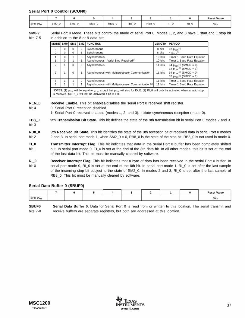
MSC1200 37SBAS289C www.ti.com
7 6 5 4 3 2 1 0 Reset Value
SFR 99H 00H
SBUF0 Serial Data Buffer 0. Data for Serial Port 0 is read from or written to this location. The serial transmit andbits 7-0 receive buffers are separate registers, but both are addressed at this location.
Serial Data Buffer 0 (SBUF0)
SM0-2 Serial Port 0 Mode. These bits control the mode of serial Port 0. Modes 1, 2, and 3 have 1 start and 1 stop bitbits 7-5 in addition to the 8 or 9 data bits.
7 6 5 4 3 2 1 0 Reset Value
SFR 98H SM0_0 SM1_0 SM2_0 REN_0 TB8_0 RB8_0 TI_0 RI_0 00H
REN_0 Receive Enable. This bit enables/disables the serial Port 0 received shift register.bit 4 0: Serial Port 0 reception disabled.
1: Serial Port 0 received enabled (modes 1, 2, and 3). Initiate synchronous reception (mode 0).
TB8_0 9th Transmission Bit State. This bit defines the state of the 9th transmission bit in serial Port 0 modes 2 and 3.bit 3
RB8_0 9th Received Bit State. This bit identifies the state of the 9th reception bit of received data in serial Port 0 modesbit 2 2 and 3. In serial port mode 1, when SM2_0 = 0, RB8_0 is the state of the stop bit. RB8_0 is not used in mode 0.
TI_0 Transmitter Interrupt Flag. This bit indicates that data in the serial Port 0 buffer has been completely shiftedbit 1 out. In serial port mode 0, TI_0 is set at the end of the 8th data bit. In all other modes, this bit is set at the end
of the last data bit. This bit must be manually cleared by software.
RI_0 Receiver Interrupt Flag. This bit indicates that a byte of data has been received in the serial Port 0 buffer. Inbit 0 serial port mode 0, RI_0 is set at the end of the 8th bit. In serial port mode 1, RI_0 is set after the last sample
of the incoming stop bit subject to the state of SM2_0. In modes 2 and 3, RI_0 is set after the last sample ofRB8_0. This bit must be manually cleared by software.
MODE SM0 SM1 SM2 FUNCTION LENGTH PERIOD
0 0 0 0 Synchronous 8 bits 12 pCLK(1)
0 0 0 1 Synchronous 8 bits 4 pCLK(1)
1 0 1 0 Asynchronous 10 bits Timer 1 Baud Rate Equation1 0 1 1 Asynchronous—Valid Stop Required(2) 10 bits Timer 1 Baud Rate Equation
2 1 0 0 Asynchronous 11 bits 64 pCLK(1) (SMOD = 0)
32 pCLK(1) (SMOD = 1)
2 1 0 1 Asynchronous with Multiprocessor Communication 11 bits 64 pCLK(1) (SMOD = 0)
32 pCLK(1) (SMOD = 1)
3 1 1 0 Asynchronous 11 bits Timer 1 Baud Rate Equation3 1 1 1 Asynchronous with Multiprocessor Communication(3) 11 bits Timer 1 Baud Rate Equation
NOTES: (1) pCLK will be equal to tCLK, except that pCLK will stop for IDLE. (2) RI_0 will only be activated when a valid stopis received. (3) RI_0 will not be activated if bit 9 = 0.
Serial Port 0 Control (SCON0)

MSC120038SBAS289Cwww.ti.com
SPI Control (SPICON) (SERSEL bit determines SPICON control)
SBIT3-0 Serial Bit Count. Number of bits transferred (read only).bits 7-4 SBIT3:0 COUNT
0x00 00x01 10x03 20x02 30x06 40x07 50x05 60x04 70x0C 8
7 6 5 4 3 2 1 0 Reset Value
SFR 9AH SBIT3 SBIT2 SBIT1 SBIT0 ORDER CPHA ESS CPOL 00H
ORDER Set Bit Order for Transmit and Receive.bit 3 0: Most Significant Bits First
1: Least Significant Bits First
CPHA Serial Clock Phase Control.bit 2 0: Valid data starting from half SCK period before the first edge of SCK
1: Valid data starting from the first edge of SCK
ESS Enable Slave Select.bit 1 0: SS (P1.4) is configured as a general-purpose I/O (default).
1: SS (P1.4) is configured as SS for SPI mode. DOUT (P1.2) drives when SS is low, and DOUT (P1.2) is high-impedance when SS is high.
CPOL Serial Clock Polarity.bit 0 0: SCK idle at logic LOW
1: SCK idle at logic HIGH
7 6 5 4 3 2 1 0 Reset Value
SFR 9AH SBIT3 SBIT2 SBIT1 SBIT0 STOP START DCS CNTSEL 00H
I2C Control (I2CCON) (SERSEL bit determines I2CCON control)
SBIT3-0 Serial Bit Count. Number of bits transferred (read only).bits 7-4 SBIT3:0 COUNT
0x00 00x01 10x03 20x02 30x06 40x07 50x05 60x04 70x0C 8
STOP Stop-Bit Status.bit 3 0: No Stop
1: Stop Condition Received and I2CCNT set (cleared on write to I2CDATA)
START Start-Bit Status.bit 2 0: No Stop
1: Start or Repeated Start Condition Received and I2CCNT set (cleared on write to I2CDATA)

MSC1200 39SBAS289C www.ti.com
7 6 5 4 3 2 1 0 Reset Value
SFR A4H SECIP SUMIP ADCIP MSECIP I2CIP CNTIP ALVDIP Unused 00H
SECIP Second System Timer Interrupt Poll (before IRQ masking).bit 7 0 = Seconds System Timer Interrupt Poll Inactive
1 = Seconds System Timer Interrupt Poll Active
SUMIP Accumulator Interrupt Poll (before IRQ masking).bits 6 0 = Accumulator Interrupt Poll Inactive
1 = Accumulator Interrupt Poll Active
ADCIP ADC Interrupt Poll (before IRQ masking).bits 5 0 = ADC Interrupt Poll Inactive
1 = ADC Interrupt Poll Active
MSECIP Millisecond System Timer Interrupt Poll (before IRQ masking).bits 4 0 = Millisecond System Timer Interrupt Poll Inactive
1 = Millisecond System Timer Interrupt Poll Active
I2CIP I2C Interrupt Poll (before IRQ masking).bits 3 0 = I2C Interrupt Poll Inactive
1 = I2C Interrupt Poll Active
CNTIP Serial Bit Count Interrupt Poll (before IRQ masking).bits 2 0 = Serial Bit Count Interrupt Poll Inactive
1 = Serial Bit Count Interrupt Poll Active
ALVDIP Analog Low Voltage Detect Interrupt Poll (before IRQ masking).bits 1 0 = Analog Low Voltage Detect Interrupt Poll Inactive
1 = Analog Low Voltage Detect Interrupt Poll Active
Auxilliary Interrupt Poll (AIPOL)
7 6 5 4 3 2 1 0 Reset Value
SFR 9BH 00H
SPIDATA SPI Data Register. Data for SPI is read from or written to this location. The SPI transmit and receive buffersbits 7-0 are separate registers, but both are addressed at this location.
I2CDATA I2C Data Register. Data for I2C is read from or written to this location. The I2C transmit and receive buffersbits 7-0 are separate registers, but both are addressed at this location.
SPI Data Register (SPIDATA) / I2C Data Register (I2CDATA)
DCS Disable Serial Clock Stretch.bit 1 0: Enable SCL Stretch (cleared by firmware or START condition)
1: Disable SCL Stretch
CNTSEL Counter Select.bit 0 0: Counter IRQ Set for Bit Counter = 8 (default)
1: Counter IRQ Set for Bit Counter = 1

MSC120040SBAS289Cwww.ti.com
7 6 5 4 3 2 1 0 Reset Value
SFR A6H ESEC ESUM EADC EMSEC EI2C ECNT EALV 0 00H
Auxiliary Interrupt Enable (AIE)
Interrupts are enabled by EICON.4 (SFR D8H). The other interrupts are controlled by the IE and EIE registers.
ESEC Enable Second System Timer Interrupt (lowest priority auxiliary interrupt).bit 7 Write: Set mask bit for this interrupt; 0 = masked, 1 = enabled.
Read: Second Timer Interrupt mask.
ESUM Enable Summation Interrupt.bit 6 Write: Set mask bit for this interrupt; 0 = masked, 1 = enabled.
Read: Summation Interrupt mask.
EADC Enable ADC Interrupt.bit 5 Write: Set mask bit for this interrupt; 0 = masked, 1 = enabled.
Read: ADC Interrupt mask.
EMSEC Enable Millisecond System Timer Interrupt.bit 4 Write: Set mask bit for this interrupt; 0 = masked, 1 = enabled.
Read: Millisecond System Timer Interrupt mask.
EI2C Enable I2C Start/Stop Bit.bit 3 Write: Set mask bit for this interrupt; 0 = masked, 1 = enabled.
Read: I2C Start/Stop Bit mask.
ECNT Enable Serial Bit Count Interrupt.bit 2 Write: Set mask bit for this interrupt; 0 = masked, 1 = enabled.
Read: Serial Bit Count Interrupt mask.
EALV Enable Analog Low Voltage Interrupt.bit 1 Write: Set mask bit for this interrupt; 0 = masked, 1 = enabled.
Read: Analog Low Voltage Detect Interrupt mask.
7 6 5 4 3 2 1 0 Reset Value
SFR A5H 0 0 0 0 PAI3 PAI2 PAI1 PAI0 00H
PAI3 PAI2 PAI1 PAI0 AUXILIARY INTERRUPT STATUS
0 0 0 0 No Pending Auxiliary IRQ
0 0 0 1 Reserved
0 0 1 0 Analog Low Voltage Detect IRQ and Possible Lower Priority Pending
0 0 1 1 I2C IRQ and Possible Lower Priority Pending
0 1 0 0 Serial Bit Count Interrupt and Possible Lower Priority Pending
0 1 0 1 Millisecond System Timer IRQ and Possible Lower Priority Pending
0 1 1 0 ADC IRQ and Possible Lower Priority Pending
0 1 1 1 Accumulator IRQ and Possible Lower Priority Pending
1 0 0 0 Second System Timer IRQ and Possible Lower Priority Pending
Pending Auxiliary Interrupt (PAI)
PAI Pending Auxiliary Interrupt Register. The results of this register can be used as an index to vector to the appropriatebits 3-0 interrupt routine. All of these interrupts vector through address 0033H.

MSC1200 41SBAS289C www.ti.com
Interrupt Enable (IE)
EA Global Interrupt Enable. This bit controls the global masking of all interrupts except those in AIE (SFR A6H).bit 7 0: Disable interrupt sources. This bit overrides individual interrupt mask settings for this register.
1: Enable all individual interrupt masks. Individual interrupts in this register will occur if enabled.
ES0 Enable Serial port 0 interrupt. This bit controls the masking of the serial Port 0 interrupt.bit 4 0: Disable all serial Port 0 interrupts.
1: Enable interrupt requests generated by the RI_0 (SCON0.0, SFR 98H) or TI_0 (SCON0.1, SFR 98H) flags.
ET1 Enable Timer 1 Interrupt. This bit controls the masking of the Timer 1 interrupt.bit 3 0: Disable Timer 1 interrupt.
1: Enable interrupt requests generated by the TF1 flag (TCON.7, SFR 88H).
EX1 Enable External Interrupt 1. This bit controls the masking of external interrupt 1.bit 2 0: Disable external interrupt 1.
1: Enable interrupt requests generated by the INT1 pin.
ET0 Enable Timer 0 Interrupt. This bit controls the masking of the Timer 0 interrupt.bit 1 0: Disable all Timer 0 interrupts.
1: Enable interrupt requests generated by the TF0 flag (TCON.5, SFR 88H).
EX0 Enable External Interrupt 0. This bit controls the masking of external interrupt 0.bit 0 0: Disable external interrupt 0.
1: Enable interrupt requests generated by the INT0 pin.
Auxiliary Interrupt Status Register (AISTAT)7 6 5 4 3 2 1 0 Reset Value
SFR A7H SEC SUM ADC MSEC I2C CNT ALVD 0 00H
SEC Second System Timer Interrupt Status Flag (lowest priority AI).bit 7 0: SEC Interrupt cleared or masked.
1: SEC Interrupt active (it is cleared by reading SECINT, SFR F9H).
SUM Summation Register Interrupt Status Flag.bit 6 0: SUM Interrupt cleared or masked.
1: SUM Interrupt active (it is cleared by reading the lowest byte of SUMR0, SFR E2H).
ADC ADC Interrupt Status Flag.bit 5 0: ADC Interrupt cleared or masked.
1: ADC Interrupt active (it is cleared by reading the lowest byte of ADRESL, SFR D9H; if active, no new data will bewritten to the ADC Results registers).
MSEC Millisecond System Timer Interrupt Status Flag.bit 4 0: MSEC Interrupt cleared or masked.
1: MSEC Interrupt active (it is cleared by reading MSINT, SFR FAH).
I2C I2C Start/Stop Interrupt Status Flag.bit 3 0: I2C Start/stop Interrupt cleared or masked.
1: I2C Start/stop Interrupt active (it is cleared by writing to I2CDATA, SFR 9BH).
CNT CNT Interrupt Status Flag.bit 2 0: CNT Interrupt cleared or masked.
1: CNT Interrupt active (it is cleared by reading from or writing to SPIDATA/I2CDATA, SFR 9BH).
ALVD Analog Low Voltage Detect Interrupt Status Flag.bit 1 0: ALVD Interrupt cleared or masked.
1: ALVD Interrupt active (cleared in HW if AVDD exceeds ALVD threshold).
NOTE: If an interrupt is masked, the status can be read in AIPOL, SFR A4H.
7 6 5 4 3 2 1 0 Reset Value
SFR A8H EA 0 0 ES0 ET1 EX1 ET0 EX0 00H

MSC120042SBAS289Cwww.ti.com
P1.1 Port 1 bit 1 control.bits 3-2
Port 1 Data Direction High Register (P1DDRH)
P1.0 Port 1 bit 0 control.bits 1-0
P11H P11L
0 0 Standard 80510 1 CMOS Output1 0 Open Drain Output1 1 Input
P1.7 Port 1 bit 7 control.bits 7-6
7 6 5 4 3 2 1 0 Reset Value
SFR AFH P17H P17L P16H P16L P15H P15L P14H P14L 00H
P17H P17L
0 0 Standard 80510 1 CMOS Output1 0 Open Drain Output1 1 Input
P1.6 Port 1 bit 6 control.bits 5-4 P16H P16L
0 0 Standard 80510 1 CMOS Output1 0 Open Drain Output1 1 Input
P1.5 Port 1 bit 5 control.bits 3-2 P15H P15L
0 0 Standard 80510 1 CMOS Output1 0 Open Drain Output1 1 Input
P1.4 Port 1 bit 4 control.bits 1-0 P14H P14L
0 0 Standard 80510 1 CMOS Output1 0 Open Drain Output1 1 Input
Port 1 Data Direction Low Register (P1DDRL)
P1.3 Port 1 bit 3 control.bits 7-6
7 6 5 4 3 2 1 0 Reset Value
SFR AEH P13H P13L P12H P12L P11H P11L P10H P10L 00H
P13H P13L
0 0 Standard 80510 1 CMOS Output1 0 Open Drain Output1 1 Input
P1.2 Port 1 bit 2 control.bits 5-4 P12H P12L
0 0 Standard 80510 1 CMOS Output1 0 Open Drain Output1 1 Input
P10H P10L
0 0 Standard 80510 1 CMOS Output1 0 Open Drain Output1 1 Input

MSC1200 43SBAS289C www.ti.com
7 6 5 4 3 2 1 0 Reset Value
SFR B3H P33H P33L P32H P32L P31H P31L P30H P30L 00H
P33H P33L
0 0 Standard 80510 1 CMOS Output1 0 Open Drain Output1 1 Input
P32H P32L
0 0 Standard 80510 1 CMOS Output1 0 Open Drain Output1 1 Input
P31H P31L
0 0 Standard 80510 1 CMOS Output1 0 Open Drain Output1 1 Input
P30H P30L
0 0 Standard 80510 1 CMOS Output1 0 Open Drain Output1 1 Input
7 6 5 4 3 2 1 0 Reset Value
SFR B0H P3.7 P3.6 P3.5 P3.4 P3.3 P3.2 P3.1 P3.0 FFH
SCK/SCL/CLKS T1 T0 INT1 INT0 TXD0 RXD0
Port 3 (P3)
P3.7-0 General-Purpose I/O Port 3. This register functions as a general-purpose I/O port. In addition, all the pins havebits 7-0 an alternative function listed below. Each of the functions is controlled by several other SFRs. The associated
Port 3 latch bit must contain a logic ‘1’ before the pin can be used in its alternate function capacity.
SCK/SCL/CLKS Clock Source Select. Refer to PASEL (SFR F2H).bit 6
T1 Timer/Counter 1 External Input. A 1 to 0 transition on this pin will increment Timer 1.bit 5
T0 Timer/Counter 0 External Input. A 1 to 0 transition on this pin will increment Timer 0.bit 4
INT1 External Interrupt 1. A falling edge/low level on this pin will cause an external interrupt 1 if enabled.bit 3
INT0 External Interrupt 0. A falling edge/low level on this pin will cause an external interrupt 0 if enabled.bit 2
TXD0 Serial Port 0 Transmit. This pin transmits the serial Port 0 data in serial port modes 1, 2, 3, and emits thebit 1 synchronizing clock in serial port mode 0.
RXD0 Serial Port 0 Receive. This pin receives the serial Port 0 data in serial port modes 1, 2, 3, and is a bidirectionalbit 0 data transfer pin in serial port mode 0.
Port 3 Data Direction Low Register (P3DDRL)
P3.3 Port 3 bit 3 control.bits 7-6
P3.2 Port 3 bit 2 control.bits 5-4
P3.1 Port 3 bit 1 control.bits 3-2
P3.0 Port 3 bit 0 control.bits 1-0

MSC120044SBAS289Cwww.ti.com
Port 3 Data Direction High Register (P3DDRH)
7 6 5 4 3 2 1 0 Reset Value
SFR B4H P37H P37L P36H P36L P35H P35L P34H P34L 00H
P3.7 Port 3 bit 7 control.bits 7-6
P3.6 Port 3 bit 6 control.bits 5-4
P3.5 Port 3 bit 5 control.bits 3-2
P3.4 Port 3 bit 4 control.bits 1-0
P36H P36L
0 0 Standard 80510 1 CMOS Output1 0 Open Drain Output1 1 Input
P35H P35L
0 0 Standard 80510 1 CMOS Output1 0 Open Drain Output1 1 Input
P34H P34L
0 0 Standard 80510 1 CMOS Output1 0 Open Drain Output1 1 Input
P37H P37L
0 0 Standard 80510 1 CMOS Output1 0 Open Drain Output1 1 Input
7 6 5 4 3 2 1 0 Reset Value
SFR B5H 00H
NOTE: Port 3.7 also controlled by EA and Memory Access Control HCR1.1.
NOTE: Port 3.6 also controlled by EA and Memory Access Control HCR1.1.
IDAC Register
IDAC IDAC Register.bits 7-0 IDACOUT = IDAC • 3.8µA (~1mA full-scale). Setting (PDCON.PDIDAC) will shut down IDAC and float the IDAC pin.
Interrupt Priority (IP)
PS0 Serial Port 0 Interrupt. This bit controls the priority of the serial Port 0 interrupt.bit 4 0 = Serial Port 0 priority is determined by the natural priority order.
1 = Serial Port 0 is a high priority interrupt.
PT1 Timer 1 Interrupt. This bit controls the priority of the Timer 1 interrupt.bit 3 0 = Timer 1 priority is determined by the natural priority order.
1 = Timer 1 priority is a high priority interrupt.
PX1 External Interrupt 1. This bit controls the priority of external interrupt 1.bit 2 0 = External interrupt 1 priority is determined by the natural priority order.
1 = External interrupt 1 is a high priority interrupt.
PT0 Timer 0 Interrupt. This bit controls the priority of the Timer 0 interrupt.bit 1 0 = Timer 0 priority is determined by the natural priority order.
1 = Timer 0 priority is a high priority interrupt.
PX0 External Interrupt 0. This bit controls the priority of external interrupt 0.bit 0 0 = External interrupt 0 priority is determined by the natural priority order.
1 = External interrupt 0 is a high priority interrupt.
7 6 5 4 3 2 1 0 Reset Value
SFR B8H 1 0 0 PS0 PT1 PX1 PT0 PX0 80H

MSC1200 45SBAS289C www.ti.com
Auxiliary interrupts will wake up from IDLE. They are enabled with EAI (EICON.5).
EWUWDT Enable Wake Up Watchdog Timer. Wake up using watchdog timer interrupt.bit 2 0 = Don’t wake up on watchdog timer interrupt.
1 = Wake up on watchdog timer interrupt.
EWUEX1 Enable Wake Up External 1. Wake up using external interrupt source 1.bit 1 0 = Don’t wake up on external interrupt source 1.
1 = Wake up on external interrupt source 1.
EWUEX0 Enable Wake Up External 0. Wake up using external interrupt source 0.bit 0 0 = Don’t wake up on external interrupt source 0.
1 = Wake up on external interrupt source 0.
System Clock Divider Register (SYSCLK)
Enable Wake Up (EWU) Waking Up from IDLE Mode
7 6 5 4 3 2 1 0 Reset Value
SFR C6H — — — — — EWUWDT EWUEX1 EWUEX0 00H
7 6 5 4 3 2 1 0 Reset Value
SFR C7H 0 0 DIVMOD1 DIVMOD0 0 DIV2 DIV1 DIV0 00H
DIVMOD DIVIDE MODE
00 Normal mode (default, no divide)
01 Immediate mode: start divide immediately, return to Normal mode on IDLE wakeup condition or Normal mode write.
10 Delay mode: same as Immediate mode, except that the mode changes with the millisecond interrupt (MSINT). If MSINT isenabled, the divide will start on the next MSINT and return to normal mode on the following MSINT. If MSINT is notenabled, the divide will start on the next MSINT condition (even if masked) but will not leave the divide mode until theMSINT counter overflows, which follows a wakeup condition. Can exit on Normal mode write.
11 Manual mode: start divide immediately; exit mode only on write to DIVMOD.
DIVMOD DIVISION MODE STATUS
00 No divide01 Divider is in Immediate mode10 Divider is in Delay mode11 Reserved
DIV DIVISOR
000 Divide by 2 (default) fCLK = fSYS/2001 Divide by 4 fCLK = fSYS/4010 Divide by 8 fCLK = fSYS/8011 Divide by 16 fCLK = fSYS/16100 Divide by 32 fCLK = fSYS/32101 Divide by 1024 fCLK = fSYS/1024110 Divide by 2048 fCLK = fSYS/2048111 Divide by 4096 fCLK = fSYS/4096
DIVMOD1-0 Clock Divide Modebits 5-4 Write:
Read:
DIV2-0 Divide Modebit 2-0

MSC120046SBAS289Cwww.ti.com
ADC Offset Calibration Register Middle Byte (OCM)
7 6 5 4 3 2 1 0 Reset Value
SFR D2H 00H
OCM ADC Offset Calibration Register Middle Byte. This is the middle byte of the 24-bit word that contains the ADCbits 7-0 offset calibration. A value which is written to this location will set the ADC offset calibration value.
ADC Offset Calibration Register High Byte (OCH)
7 6 5 4 3 2 1 0 Reset Value
SFR D3H MSB 00H
OCH ADC Offset Calibration Register High Byte. This is the high byte of the 24-bit word that contains thebits 7-0 ADC offset calibration. A value which is written to this location will set the ADC offset calibration value.
Program Status Word (PSW)
CY Carry Flag. This bit is set when the last arithmetic operation resulted in a carry (during addition) or a borrowbit 7 (during subtraction). Otherwise it is cleared to 0 by all arithmetic operations.
AC Auxiliary Carry Flag. This bit is set to 1 if the last arithmetic operation resulted in a carry into (during addition),bit 6 or a borrow (during substraction) from the high order nibble. Otherwise it is cleared to 0 by all arithmetic
operations.
F0 User Flag 0. This is a bit-addressable, general-purpose flag for software control.bit 5
RS1, RS0 Register Bank Select 1-0. These bits select which register bank is addressed during register accesses.bits 4-3
OV Overflow Flag. This bit is set to 1 if the last arithmetic operation resulted in a carry (addition), borrowbit 2 (subtraction), or overflow (multiply or divide). Otherwise it is cleared to 0 by all arithmetic operations.
F1 User Flag 1. This is a bit-addressable, general-purpose flag for software control.bit 1
P Parity Flag. This bit is set to 1 if the modulo-2 sum of the 8 bits of the accumulator is 1 (odd parity); andbit 0 cleared to 0 on even parity.
ADC Offset Calibration Register Low Byte (OCL)
7 6 5 4 3 2 1 0 Reset Value
SFR D0H CY AC F0 RS1 RS0 OV F1 P 00H
RS1 RS0 REGISTER BANK ADDRESS
0 0 0 00H-07H
0 1 1 08H-0FH
1 0 2 10H-17H
1 1 3 18H-1FH
OCL ADC Offset Calibration Register Low Byte. This is the low byte of the 24-bit word that contains thebits 7-0 ADC offset calibration. A value which is written to this location will set the ADC offset calibration value.
7 6 5 4 3 2 1 0 Reset Value
SFR D1H LSB 00H

MSC1200 47SBAS289C www.ti.com
GCM ADC Gain Calibration Register Middle Byte. This is the middle byte of the 24-bit word that containsbits 7-0 the ADC gain calibration. A value which is written to this location will set the ADC gain calibration value.
ADC Gain Calibration Register High Byte (GCH)
7 6 5 4 3 2 1 0 Reset Value
SFR D5H ECH
GCH ADC Gain Calibration Register High Byte. This is the high byte of the 24-bit word that contains thebits 7-0 ADC gain calibration. A value which is written to this location will set the ADC gain calibration value.
ADC Multiplexer Register (ADMUX)
7 6 5 4 3 2 1 0 Reset Value
SFR D6H MSB 5FH
INP3-0 Input Multiplexer Positive Channel. This selects the positive signal input.bits 7-4
7 6 5 4 3 2 1 0 Reset Value
SFR D7H INP3 INP2 INP1 INP0 INN3 INN2 INN1 INN0 01H
INP3 INP2 INP1 INP0 POSITIVE INPUT
0 0 0 0 AIN0 (default)0 0 0 1 AIN10 0 1 0 AIN20 0 1 1 AIN30 1 0 0 AIN40 1 0 1 AIN50 1 1 0 AIN60 1 1 1 AIN71 0 0 0 AINCOM1 1 1 1 Temperature Sensor (Requires ADMUX = FFH)
INN3-0 Input Multiplexer Negative Channel. This selects the negative signal input.bits 3-0 INN3 INN2 INN1 INN0 NEGATIVE INPUT
0 0 0 0 AIN00 0 0 1 AIN1 (default)0 0 1 0 AIN20 0 1 1 AIN30 1 0 0 AIN40 1 0 1 AIN50 1 1 0 AIN60 1 1 1 AIN71 0 0 0 AINCOM1 1 1 1 Temperature Sensor (Requires ADMUX = FFH)
ADC Gain Calibration Register Middle Byte (GCM)
GCL ADC Gain Calibration Register Low Byte. This is the low byte of the 24-bit word that contains the ADCbits 7-0 gain calibration. A value which is written to this location will set the ADC gain calibration value.
7 6 5 4 3 2 1 0 Reset Value
SFR D4H LSB 5AH
ADC Gain Calibration Register Low Byte (GCL)

MSC120048SBAS289Cwww.ti.com
ADRESL The ADC Results Low Byte. This is the low byte of the 24-bit word that contains the ADCbits 7-0 Results. Reading from this register clears the ADC interrupt; however, AI in EICON (SFR D8) must also be cleared.
ADC Results Register Middle Byte (ADRESM)
7 6 5 4 3 2 1 0 Reset Value
SFR D9H LSB 00H
7 6 5 4 3 2 1 0 Reset Value
SFR DAH 00H
ADRESM The ADC Results Middle Byte. This is the middle byte of the 24-bit word that contains the ADCbits 7-0 Results.
ADC Results Register High Byte (ADRESH)
ADRESH The ADC Results High Byte. This is the high byte of the 24-bit word that contains the ADCbits 7-0 Results.
7 6 5 4 3 2 1 0 Reset Value
SFR DBH MSB 00H
7 6 5 4 3 2 1 0 Reset Value
SFR D8H 0 1 EAI AI WDTI 0 0 0 40H
Enable Interrupt Control (EICON)
EAI Enable Auxiliary Interrupt. The Auxiliary Interrupt accesses nine different interrupts which are masked andbit 5 identified by SFR registers PAI (SFR A5H), AIE (SFR A6H), and AISTAT (SFR A7H).
0 = Auxiliary Interrupt disabled (default).1 = Auxiliary Interrupt enabled.
AI Auxiliary Interrupt Flag. AI must be cleared by software before exiting the interrupt service routine,bit 4 after the source of the interrupt is cleared. Otherwise, the interrupt occurs again. Setting AI in software generates
an Auxiliary Interrupt, if enabled.0 = No Auxiliary Interrupt detected (default).1 = Auxiliary Interrupt detected.
WDTI Watchdog Timer Interrupt Flag. WDTI must be cleared by software before exiting the interrupt service routine.bit 3 Otherwise, the interrupt occurs again. Setting WDTI in software generates a watchdog time interrupt, if enabled. The
Watchdog timer can generate an interrupt or reset. The interrupt is available only if the reset action is disabledin HCR0.0 = No Watchdog Timer Interrupt Detected (default).1 = Watchdog Timer Interrupt Detected.
ADC Results Register Low Byte (ADRESL)

MSC1200 49SBAS289C www.ti.com
ADC Control Register 0 (ADCON0)
7 6 5 4 3 2 1 0 Reset Value
SFR DCH — BOD EVREF VREFH EBUF PGA2 PGA1 PGA0 30H
BOD Burnout Detect. When enabled this connects a positive current source to the positive channel and a negative currentbit 6 source to the negative channel. If the channel is open circuit then the ADC results will be full-scale (buffer must be enabled).
0 = Burnout Current Sources Off (default).1 = Burnout Current Sources On.
EVREF Enable Internal Voltage Reference. If an external voltage reference is used, the internal voltage reference shouldbit 5 be disabled.
0 = Internal Voltage Reference Off.1 = Internal Voltage Reference On (default).
VREFH Voltage Reference High Select. The internal voltage reference can be selected to be 2.5V or 1.25V.bit 4 0 = REFOUT/REFIN+ is 1.25V.
1 = REFOUT/REFIN+ is 2.5V (default).
EBUF Enable Buffer. Enable the input buffer to provide higher input impedance but limits the input voltage range andbit 3 dissipates more power.
0 = Buffer disabled (default).1 = Buffer enabled.
PGA2-0 Programmable Gain Amplifier. Sets the gain for the PGA from 1 to 128.bits 2-0 PGA2 PGA1 PGA0 GAIN
0 0 0 1 (default)0 0 1 20 1 0 40 1 1 81 0 0 161 0 1 321 1 0 641 1 1 128

MSC120050SBAS289Cwww.ti.com
SM1 SM0 SETTLING MODE
0 0 Auto0 1 Fast Settling Filter1 0 Sinc2 Filter1 1 Sinc3 Filter
ADC Control Register 1 (ADCON1)
OF_UF Overflow/Underflow. If this bit is set, the data in the summation register is invalid. Either an overflow or anbit 7 underflow occurred. The bit is cleared by writing a 0 to it.
POL Polarity. Polarity of the ADC result and Summation register.bit 6 0 = Bipolar.
1 = Unipolar.
7 6 5 4 3 2 1 0 Reset Value
SFR DDH OF_UF POL SM1 SM0 — CAL2 CAL1 CAL0 x000 0000B
POL ANALOG INPUT DIGITAL OUTPUT
+FSR 0x7FFFFF0 ZERO 0x000000
–FSR 0x800000
+FSR 0xFFFFFF1 ZERO 0x000000
–FSR 0x000000
SM1-0 Settling Mode. Selects the type of filter or auto select which defines the digital filter settling characteristics.bits 5-4
CAL2-0 Calibration Mode Control Bits. Writing to this register initiates calibration.bits 2-0
ADC Control Register 2 (ADCON2)
CAL2 CAL1 CAL0 CALIBRATION MODE
0 0 0 No Calibration (default)0 0 1 Self Calibration, Offset and Gain0 1 0 Self Calibration, Offset Only0 1 1 Self Calibration, Gain Only1 0 0 System Calibration, Offset Only1 0 1 System Calibration, Gain Only1 1 0 Reserved1 1 1 Reserved
DR7-0 Decimation Ratio LSB (refer to ADCON3, SFR DFH).bits 7-0
ADC Control Register 3 (ADCON3)
7 6 5 4 3 2 1 0 Reset Value
SFR DEH DR7 DR6 DR5 DR4 DR3 DR2 DR1 DR0 1BH
DR10-8 Decimation Ratio Most Significant 3 Bits. The output data rate = f
DecimationRatioMOD
where fMOD = f
ACLKCLK
( )+ •1 64 .bits 2-0
Accumulator (A or ACC)
7 6 5 4 3 2 1 0 Reset Value
SFR E0H ACC.7 ACC.6 ACC.5 ACC.4 ACC.3 ACC.2 ACC.1 ACC.0 00H
ACC.7-0 Accumulator. This register serves as the accumulator for arithmetic and logic operations.bits 7-0
Summation/Shifter Control (SSCON)
7 6 5 4 3 2 1 0 Reset Value
SFR E1H SSCON1 SSCON0 SCNT2 SCNT1 SCNT0 SHF2 SHF1 SHF0 00H
Read Value—000B.
7 6 5 4 3 2 1 0 Reset Value
SFR DFH — — — — — DR10 DR9 DR8 06H
The Summation register is powered down when the ADC is powered down. If all zeroes are written to this register the 32-bitSUMR3-0 registers will be cleared. The Summation registers will do sign extend if Bipolar is selected in ADCON1.

MSC1200 51SBAS289C www.ti.com
SHF2-0 Shift Count.bits 2-0
SUMR0 Summation Register 0. This is the least significant byte of the 32-bit summation register or bits 0 to 7.bits 7-0 Write: will cause values in SUMR3-0 to be added to or subtracted from the summation register.
Read: will clear the Summation Interrupt.
Summation Register 1 (SUMR1)
SHF2 SHF1 SHF0 SHIFT DIVIDE
0 0 0 1 20 0 1 2 40 1 0 3 80 1 1 4 161 0 0 5 321 0 1 6 641 1 0 7 1281 1 1 8 256
7 6 5 4 3 2 1 0 Reset Value
SFR E2H LSB 00H
SUMR1 Summation Register 1. This is the most significant byte of the lowest 16 bits of the summation register or bits 8-15.bits 7-0
Summation Register 2 (SUMR2)
7 6 5 4 3 2 1 0 Reset Value
SFR E3H 00H
SUMR2 Summation Register 2. This is the most significant byte of the lowest 24 bits of the summation register or bits 16-23.bits 7-0
7 6 5 4 3 2 1 0 Reset Value
SFR E4H 00H
SSCON1-0 Summation/Shift Control.bits 7-6
SCNT2-0 Summation Count. When the summation is complete an interrupt will be generated unless masked. Reading thebits 5-3 SUMR0 register clears the interrupt.
SCNT2 SCNT1 SCNT0 SUMMATION COUNT
0 0 0 20 0 1 40 1 0 80 1 1 161 0 0 321 0 1 641 1 0 1281 1 1 256
SSCON1 SSCON0 SCNT2 SCNT1 SCNT0 SHF2 SHF1 SHF0 DESCRIPTION
0 0 0 0 0 0 0 0 Clear Summation Register0 0 0 1 0 0 0 0 CPU Summation on Write to SUMR00 0 1 0 0 0 0 0 CPU Subtraction on Write to SUMR01 0 x x x Note (1) Note (1) Note (1) CPU Shift Only0 1 Note (1) Note (1) Note (1) x x x ADC Summation Only1 1 Note (1) Note (1) Note (1) Note (1) Note (1) Note (1) ADC Summation Completes then Shift Completes
NOTES: (1) Refer to register bit definition.
7 6 5 4 3 2 1 0 Reset Value
SFR E5H MSB 00H
Summation Register 3 (SUMR3)
SUMR3 Summation Register 3. This is the most significant byte of the 32-bit summation register or bits 24-31.bits 7-0
Summation Register 0 (SUMR0)

MSC120052SBAS289Cwww.ti.com
Low Voltage Detect Control (LVDCON)
ALVDIS Analog Low Voltage Detect Disable.bit 7 0 = Enable Detection of Low Analog Supply Voltage (ALVD interrupt set when AVDD < 2.8V).
1 = Disable Detection of Low Analog Supply Voltage.
7 6 5 4 3 2 1 0 Reset Value
SFR E7H ALVDIS 0 0 0 1 1 1 1 8FH
Extended Interrupt Enable (EIE)
7 6 5 4 3 2 1 0 Reset Value
SFR E8H 1 1 1 EWDI EX5 EX4 EX3 EX2 E0H
EWDI Enable Watchdog Interrupt. This bit enables/disables the watchdog interrupt. The Watchdog timer is enabled bythe WDTCON (SFR FFH) and PDCON (SFR F1H) registers.
bit 4 0 = Disable the Watchdog Interrupt1 = Enable Interrupt Request Generated by the Watchdog Timer
EX5 External Interrupt 5 Enable. This bit enables/disables external interrupt 5.bit 3 0 = Disable External Interrupt 5
1 = Enable External Interrupt 5
EX4 External Interrupt 4 Enable. This bit enables/disables external interrupt 4.bit 2 0 = Disable External Interrupt 4
1 = Enable External Interrupt 4
EX3 External Interrupt 3 Enable. This bit enables/disables external interrupt 3.bit 1 0 = Disable External Interrupt 3
1 = Enable External Interrupt 3
EX2 External Interrupt 2 Enable. This bit enables/disables external interrupt 2.bit 0 0 = Disable External Interrupt 2
1 = Enable External Interrupt 2
Offset DAC Register (ODAC)
ODAC Offset DAC Register. This register will shift the input by up to half of the ADC full-scale input range. The offsetbit7-0 DAC value is summed from the ADC input prior to conversion. Writing 00H or 80H to ODAC turns off the Offset DAC.
bit 7 Offset DAC Sign bit.0 = Positive1 = Negative
bit 6-0 Offset = V
PGAODACREF bit
26 0
1271 7
••
• −[ : ]( )
NOTE: The offset must be used after calibration or the calibration will nullify the effects.
7 6 5 4 3 2 1 0 Reset Value
SFR E6H 00H

MSC1200 53SBAS289C www.ti.com
Hardware Product Code Register 0 (HWPC0)
HWPC0.7-0 Hardware Product Code LSB. Read only.bits 7-0
7 6 5 4 3 2 1 0 Reset Value
SFR E9H 0 0 0 0 0 0 0 MEMORY 0000_000xB
7 6 5 4 3 2 1 0 Reset Value
SFR EAH 0 0 1 0 0 0 0 0 20H
HWPC1.7-0 Hardware Product Code MSB. Read only.bits 7-0
Hardware Version Register (HWVER)
PGERA Page Erase. Available in both user and program modes.bit 6 0 = Disable Page Erase Mode
1 = Enable Page Erase Mode
FRCM Frequency Control Mode. The bypass is only used for slow clocks to save power.bit 4 0 = Bypass (default)
1 = Use Delay Line. Saves power (Recommended).
BUSY Write/Erase BUSY Signal.bit 2 0 = Idle or Available
1 = Busy
Flash Memory Timing Control Register (FTCON)
7 6 5 4 3 2 1 0 Reset Value
SFR EEH 0 PGERA 0 FRCM 0 BUSY 1 0 02H
7 6 5 4 3 2 1 0 Reset Value
SFR EFH FER3 FER2 FER1 FER0 FWR3 FWR2 FWR1 FWR0 A5H
MEMORY SIZE MODEL FLASH MEMORY
0 MSC1200Y2 4kB1 MSC1200Y3 8kB
Hardware Product Code Register 1 (HWPC1)
Refer to Flash Timing Characteristics
FER3-0 Set Erase. Flash Erase Time = (1 + FER) • (MSEC + 1) • tCLK.bits 7-4 11ms industrial temperature range.
5ms commercial temperature range.
FWR3-0 Set Write. Flash Write Time = (1 + FWR) • (USEC + 1) • 5 • tCLK.bits 3-0 30µs to 40µs.
7 6 5 4 3 2 1 0 Reset Value
SFR EBH
Flash Memory Control (FMCON)
B Register (B)
B B Register. This register serves as a second accumulator for certain arithmetic operations.bits 7-0
7 6 5 4 3 2 1 0 Reset Value
SFR F0H 00H

MSC120054SBAS289Cwww.ti.com
PSEN4-0 PSEN Mode Select. Defines the output on P3.6 in User Application mode or Serial Flash Programming mode.bits 7-3 00000: General-Purpose I/O (default)
00001: SYSCLK00011: Internal PSEN (refer to Figure 3 for timing)00101: Internal ALE (refer to Figure 3 for timing)00111: fOSC(buffered XIN oscillator clock)01001: Memory WR (MOVX write)01011: T0 Out (overflow)(1)
01101: T1 Out (overflow)(1)
01111: fMOD(2)
10001: SYSCLK/2 (toggles on rising edge)(2)
10011: Internal PSEN/2(2)
10101: Internal ALE/2(2)
10111: fOSC/2(2)
11001: Memory WR/2 (MOVX write)(2)
11011: T0 Out/2 (overflow)(2)
11101: T1 Out/2 (overflow)(2)
11111: fMOD/2(2)
NOTES: (1) On period of these signals equal to tCLK. (2) Duty cycle is 50%.
7 6 5 4 3 2 1 0 Reset Value
SFR F1H PDICLK PDIDAC PDI2C 0 PDADC PDWDT PDSPI PDSPI 6FH
Turning peripheral modules off puts the MSC1200 in the lowest power mode.
PDICLK Internal Clock Control.bit 7 0 = Internal Oscillator and PLL On (Internal Oscillator or PLL mode)
1 = Internal Oscillator and PLL Power Down (External Clock mode)
PDIDAC IDAC Control.bit 6 0 = IDAC On
1 = IDAC Power Down (default)
PDI2C I2C Control.bit 5 0 = I2C On (only when PDSPI = 1)
1 = I2C Power Down (default)
PDADC ADC Control.bit 3 0 = ADC On
1 = ADC, VREF, and Summation registers are powered down (default).
PDWDT Watchdog Timer Control.bit 2 0 = Watchdog Timer On
1 = Watchdog Timer Power Down (default)
PDST System Timer Control.bit 1 0 = System Timer On
1 = System Timer Power Down (default)
PDSPI SPI Control.bit 0 0 = SPI System On
1 = SPI System Power Down (default)
PSEN/ALE Select (PASEL)7 6 5 4 3 2 1 0 Reset Value
SFR F2H PSEN4 PSEN3 PSEN2 PSEN1 PSEN0 0 0 0 00H
Power-Down Control Register (PDCON)

MSC1200 55SBAS289C www.ti.com
Analog Clock (ACLK)
FREQ6-0 Clock Frequency – 1. This value + 1 divides the system clock to create the ADC clock.
bits 6-0 fACLK = f
ACLKCLK
( )+1 , where fCLK = f
SYSCLK DividerOSC
.
fMOD = fACLK
64
ADC Data Rate = fDATA = f
DecimationRatioMOD
System Reset Register (SRST)
7 6 5 4 3 2 1 0 Reset Value
SFR F7H 0 0 0 0 0 0 0 RSTREQ 00H
7 6 5 4 3 2 1 0 Reset Value
SFR F6H 0 FREQ6 FREQ5 FREQ4 FREQ3 FREQ2 FREQ1 FREQ0 03H
RSTREQ Reset Request. Setting this bit to 1 and then clearing to 0 will generate a system reset.bit 0
PLL7-0 PLL Counter Value Least Significant Bit.bits 7-0
PLL Frequency = External Crystal Frequency • PLL9:0
Phase Lock Loop High Register (PLLH)
7 6 5 4 3 2 1 0 Reset Value
SFR F4H PLL7 PLL6 PLL5 PLL4 PLL3 PLL2 PLL1 PLL0 C1H
Phase Lock Loop Low Register (PLLL)
7 6 5 4 3 2 1 0 Reset Value
SFR F5H CLKSTAT2 CLKSTAT1 CLKSTAT0 PLLLOCK 0 0 PLL9 PLL8 x1H
CLKSTAT2-0 Active Clock Status (read only). Derived from HCR2 setting; refer to Table II.bits 7-5 000: Reserved
001: Reserved010: Reserved011: External Clock Mode100: PLL High-Frequency (HF) Mode (must read PLLLOCK to determine active clock status)101: PLL Low-Frequency (LF) Mode (must read PLLLOCK to determine active clock status)110: Internal Oscillator High-Frequency (HF) Mode111: Internal Oscillator Low-Frequency (LF) Mode
PLLLOCK PLL Lock Status and Status Enable.bit 4 For Write (PLL Lock Status Enable):
0 = No Effect1 = Enable PLL Lock Detection (must wait 20ms before PLLLOCK read status is valid).
For Read (PLL Lock Status):0 = PLL Not Locked (PLL may be inactive; refer to Table II for active clock mode)1 = PLL Locked (PLL is active clock)
PLL9-8 PLL Counter Value Most Significant 2 Bits (refer to PLLL, SFR F4H)bits 1-0

MSC120056SBAS289Cwww.ti.com
The clock used for this timer is the 1ms clock which results from dividing the system clock by the values in registers MSECH:MSECL.Reading this register will clear MSINT.
WRT Write Control. Determines whether to write the value immediately or wait until the current count is finished. Read = 0.bit 7 0 = Delay Write Operation. The MSINT value is loaded when the current count expires.
1 = Write Immediately. The MSINT counter is loaded once the CPU completes the write operation.
MSINT6-0 Seconds Count. Normal operation would use 1ms as the clock interval.bits 6-0 MS Interrupt Interval = (1 + MSINT) • (MSEC + 1) • tCLK
7 6 5 4 3 2 1 0 Reset Value
SFR FAH WRT MSINT6 MSINT5 MSINT4 MSINT3 MSINT2 MSINT1 MSINT0 7FH
Milliseconds Interrupt (MSINT)
7 6 5 4 3 2 1 0 Reset Value
SFR F8H 1 1 1 PWDI PX5 PX4 PX3 PX2 E0H
7 6 5 4 3 2 1 0 Reset Value
SFR F9H WRT SECINT6 SECINT5 SECINT4 SECINT3 SECINT2 SECINT1 SECINT0 7FH
This system clock is divided by the value of the 16-bit register MSECH:MSECL. Then that 1ms timer tick is divided by the registerHMSEC which provides the 100ms signal used by this seconds timer. Therefore, this seconds timer can generate an interruptwhich occurs from 100ms to 12.8 seconds. Reading this register will clear the Seconds Interrupt. This Interrupt can be monitoredin the AIE register.
WRT Write Control. Determines whether to write the value immediately or wait until the current count is finished.bit 7 Read = 0.
0 = Delay Write Operation. The SEC value is loaded when the current count expires.1 = Write Immediately. The counter is loaded once the CPU completes the write operation.
SECINT6-0 Seconds Count. Normal operation would use 100ms as the clock interval.bits 6-0 Seconds Interrupt = (1 + SEC) • (HMSEC + 1) • (MSEC + 1) • tCLK.
PWDI Watchdog Interrupt Priority. This bit controls the priority of the watchdog interrupt.bit 4 0 = The watchdog interrupt is low priority.
1 = The watchdog interrupt is high priority.
PX5 External Interrupt 5 Priority. This bit controls the priority of external interrupt 5.bit 3 0 = External interrupt 5 is low priority.
1 = External interrupt 5 is high priority.
PX4 External Interrupt 4 Priority. This bit controls the priority of external interrupt 4.bit 2 0 = External interrupt 4 is low priority.
1 = External interrupt 4 is high priority.
PX3 External Interrupt 3 Priority. This bit controls the priority of external interrupt 3.bit 1 0 = External interrupt 3 is low priority.
1 = External interrupt 3 is high priority.
PX2 External Interrupt 2 Priority. This bit controls the priority of external interrupt 2.bit 0 0 = External interrupt 2 is low priority.
1 = External interrupt 2 is high priority.
Seconds Timer Interrupt (SECINT)
Extended Interrupt Priority (EIP)

MSC1200 57SBAS289C www.ti.com
FREQ5-0 Clock Frequency – 1. This value + 1 divides the system clock to create a 1µs Clock.bits 5-0 USEC = CLK/(FREQ + 1). This clock is used to set Flash write time. See FTCON (SFR EFH).
One Millisecond Low Register (MSECL)
MSECL7-0 One Millisecond Low. This value in combination with the next register is used to create a 1ms Clock.bits 7-0 1ms Clock = (MSECH • 256 + MSECL + 1) • tCLK. This clock is used to set Flash erase time. See FTCON (SFR EFH).
One Millisecond High Register (MSECH)
7 6 5 4 3 2 1 0 Reset Value
SFR FBH 0 0 FREQ5 FREQ4 FREQ3 FREQ2 FREQ1 FREQ0 03H
7 6 5 4 3 2 1 0 Reset Value
SFR FDH MSECH7 MSECH6 MSECH5 MSECH4 MSECH3 MSECH2 MSECH1 MSECH0 0FH
7 6 5 4 3 2 1 0 Reset Value
SFR FCH MSECL7 MSECL6 MSECL5 MSECL4 MSECL3 MSECL2 MSECL1 MSECL0 9FH
MSECH7-0 One Millisecond High. This value in combination with the previous register is used to create a 1ms clock.bits 7-0 1ms = (MSECH • 256 + MSECL + 1) • tCLK.
One Hundred Millisecond Register (HMSEC)
7 6 5 4 3 2 1 0 Reset Value
SFR FEH HMSEC7 HMSEC6 HMSEC5 HMSEC4 HMSEC3 HMSEC2 HMSEC1 HMSEC0 63H
7 6 5 4 3 2 1 0 Reset Value
SFR FFH EWDT DWDT RWDT WDCNT4 WDCNT3 WDCNT2 WDCNT1 WDCNT0 00H
HMSEC7-0 One Hundred Millisecond. This clock divides the 1ms clock to create a 100ms clock.bits 7-0 100ms = (MSECH • 256 + MSECL + 1) • (HMSEC + 1) • tCLK.
Watchdog Timer Register (WDTCON)
EWDT Enable Watchdog (R/W).bit 7 Write 1/Write 0 sequence sets the Watchdog Enable Counting bit.
DWDT Disable Watchdog (R/W).bit 6 Write 1/Write 0 sequence clears the Watchdog Enable Counting bit.
RWDT Reset Watchdog (R/W).bit 5 Write 1/Write 0 sequence restarts the Watchdog Counter.
WDCNT4-0 Watchdog Count (R/W).bits 4-0 Watchdog expires in (WDCNT + 1) • HMSEC to (WDCNT + 2) • HMSEC, if the sequence is not asserted. There
is an uncertainty of 1 count.NOTE: If HCR0.3 (EWDR) is set and the watchdog timer expires, a system reset is generated. If HCR0.3 (EWDR) is clearedand the watchdog timer expires, an interrupt is generated (see Table VII).
One Microsecond Register (USEC)

MECHANICAL DATA
MTQF019A – JANUARY 1995 – REVISED JANUARY 1998
POST OFFICE BOX 655303 • DALLAS, TEXAS 75265
PFB (S-PQFP-G48) PLASTIC QUAD FLATPACK
4073176/B 10/96
Gage Plane
0,13 NOM
0,25
0,450,75
Seating Plane
0,05 MIN
0,170,27
24
25
13
12
SQ
36
37
7,206,80
48
1
5,50 TYP
SQ8,809,20
1,050,95
1,20 MAX0,08
0,50 M0,08
0°–7°
NOTES: A. All linear dimensions are in millimeters.B. This drawing is subject to change without notice.C. Falls within JEDEC MS-026

IMPORTANT NOTICE
Texas Instruments Incorporated and its subsidiaries (TI) reserve the right to make corrections, modifications,enhancements, improvements, and other changes to its products and services at any time and to discontinueany product or service without notice. Customers should obtain the latest relevant information before placingorders and should verify that such information is current and complete. All products are sold subject to TI’s termsand conditions of sale supplied at the time of order acknowledgment.
TI warrants performance of its hardware products to the specifications applicable at the time of sale inaccordance with TI’s standard warranty. Testing and other quality control techniques are used to the extent TIdeems necessary to support this warranty. Except where mandated by government requirements, testing of allparameters of each product is not necessarily performed.
TI assumes no liability for applications assistance or customer product design. Customers are responsible fortheir products and applications using TI components. To minimize the risks associated with customer productsand applications, customers should provide adequate design and operating safeguards.
TI does not warrant or represent that any license, either express or implied, is granted under any TI patent right,copyright, mask work right, or other TI intellectual property right relating to any combination, machine, or processin which TI products or services are used. Information published by TI regarding third-party products or servicesdoes not constitute a license from TI to use such products or services or a warranty or endorsement thereof.Use of such information may require a license from a third party under the patents or other intellectual propertyof the third party, or a license from TI under the patents or other intellectual property of TI.
Reproduction of information in TI data books or data sheets is permissible only if reproduction is withoutalteration and is accompanied by all associated warranties, conditions, limitations, and notices. Reproductionof this information with alteration is an unfair and deceptive business practice. TI is not responsible or liable forsuch altered documentation.
Resale of TI products or services with statements different from or beyond the parameters stated by TI for thatproduct or service voids all express and any implied warranties for the associated TI product or service andis an unfair and deceptive business practice. TI is not responsible or liable for any such statements.
Following are URLs where you can obtain information on other Texas Instruments products and applicationsolutions:
Products Applications
Amplifiers amplifier.ti.com Audio www.ti.com/audio
Data Converters dataconverter.ti.com Automotive www.ti.com/automotive
DSP dsp.ti.com Broadband www.ti.com/broadband
Interface interface.ti.com Digital Control www.ti.com/digitalcontrol
Logic logic.ti.com Military www.ti.com/military
Power Mgmt power.ti.com Optical Networking www.ti.com/opticalnetwork
Microcontrollers microcontroller.ti.com Security www.ti.com/security
Telephony www.ti.com/telephony
Video & Imaging www.ti.com/video
Wireless www.ti.com/wireless
Mailing Address: Texas Instruments
Post Office Box 655303 Dallas, Texas 75265
Copyright 2004, Texas Instruments Incorporated