msp430 i/o launchpad · 2017-09-22 · read/write operation to/from the wdtctl register must be...
TRANSCRIPT

Processor Architecture Laboratory EPFL 1 MSP430
R.Beuchat C:\Users\rbeuchat\SWITCHdrive\rb-laboratories\Enonces_Doc\MSP430_LaboDocuments\Labo_MSP430_2_4a.docx
Créé le 22/09/17 Impression le 22/09/17
Modifié le 22/09/17 07:09 Version [2.3]
MSP430 I/O LaunchPad MSP430 Laboratory
Goal Understand the operation of the MSP430 peripherals
Resource MSP430G2553 Microcontroller
Prerequisites MSP430 Base Course
Theory
Equipment MSP430G2-LaunchPad board Code composer Studio cross development tools
Duration ~6h
1 Introduction
The objective of this laboratory is to understand how to operate some of the programmable interfaces available on a microcontroller (specifically on the MSP430 family, part number G2553, available on the TI LaunchPad board).
This laboratory is divided into 3 sessions, and the final demonstration is to be able to convert an analog signal to a digital one using the Analog to Digital (A/D) converter available on the LaunchPad.
The microcontroller should output a Pulse Width Modulated (PWM) signal with a width that is proportional to the provided analog input. An oscilloscope and/or a logic analyzer will be used to display the PWM output as well as other useful signals.
Figure 1 – General system block schematic, internal ADC
uC (MSP430)
ATD
uP
+
Program
PWM

Processor Architecture Laboratory EPFL 2 MSP430
R.Beuchat C:\Users\rbeuchat\SWITCHdrive\rb-laboratories\Enonces_Doc\MSP430_LaboDocuments\Labo_MSP430_2_4a.docx
1.1 Clock
The clock subsystem is responsible for providing the clocks for the device. In the case of the MSP430G2553, it is referred to as the Basic Clock Module+ by the User guide and is shown in Fig.2.
It features three physical clock sources:
1. LFXT1CLK: a low or high frequency oscillator that requires an external clock or crystal (not present on the LaunchPad);
2. DCOCLK: an internal DCO
(https://en.wikipedia.org/wiki/Digitally_controlled_oscillator); and
3. VLOCLK: an internal very low-power, low frequency oscillator with a non-programmable frequency of about 12 kHz.
Figure 2 – Basic Clock Module+ Block Diagram

Processor Architecture Laboratory EPFL 3 MSP430
R.Beuchat C:\Users\rbeuchat\SWITCHdrive\rb-laboratories\Enonces_Doc\MSP430_LaboDocuments\Labo_MSP430_2_4a.docx
Each of these physical clock sources can be used as the source of three clock signals (Although, note that all binding are not possible according to the schematic!):
1. MCLK, stands for Main clock, the clock used by the CPU and the system; 2. SMCLK, stands for Sub-main clock; and 3. ACLK , stands for Auxiliary clock
Both the SMCLK and the ACLK can be selected to be used in certain subsystems, e.g a timer.
The clock selection logic is outlined in the schematic on the next page, and is detailed in the MSP430G2553 User guide. Make sure you feel comfortable with the control registers of the clock subsystem, i.e. the DCOCTL and BCSCTLx registers.
1.2 GPIO
The LaunchPad board has 2 I/O ports (P1 and P2). Each of these I/O ports can be used as a standard GPIO port, or can be configured as functional ports for various peripherals.
Consider, as an example, another microcontroller (MSP430F5437) used in the WSN4U board from EPFL/LAP, which has 8 I/O ports (P1 to P8).
Port Primary Function Peripheral Functions
Port 1 I/O (P1.0 to P1.7) Timer
Port 2 I/O (P2.0 to P2.7) Timer, A/D converter, DMA trigger
Port 3 I/O (P3.0 to P3.7) SPI, I2C, UART
Port 4 I/O (P4.0 to P4.7) Timer
Port 5 I/O (P5.0 to P5.7) SPI, I2C, A/C reference
Port 6 I/O (P6.0 to P6.7) A/D converter
Port 7 I/O (P7.0 to P7.7) Timer, A/D converter
Port 8 I/O (P8.0 to P8.6) Timer
Figure 3 below illustrates how a typical I/O port is organized inside the microcontroller, along with the registers that need to be configured to obtain the intended operation for each pin:
Figure 3 – Internal architecture of the Port 8
Depending on the I/O port, several registers should be configured in order to achieve the desired function. The table below summarizes the main registers and their configuration.

Processor Architecture Laboratory EPFL 4 MSP430
R.Beuchat C:\Users\rbeuchat\SWITCHdrive\rb-laboratories\Enonces_Doc\MSP430_LaboDocuments\Labo_MSP430_2_4a.docx
Register Description Configuration Comments
PxDIR Direction Register –
Input/Output 0 Input, 1 Output
PxIN Read Value Register 0 Low, 1 High
PxOUT Write Value Register 0 Low, 1 High
PxSEL Function Selection Register 0 I/O, 1 Peripheral
PxREN Resistor Enable Register 0 Disabled, 1
Enabled
If enabled, PxOUT select pull-up/down (0 Pull-down, 1 Pull-up)
PxDS Output Drive Strength Register 0 Reduced, 1 Full Full drive can increase
EMI
* In the table above, (x) represents a specific register (for Port 1, P1)
Manipulation 1 GPIO
Using the LaunchPad board schematics and the TI MSP430 documentation, write a C program that generates a pulse width modulated (PWM) signal on one of board's available I/O ports.
Test your solution with a logic analyzer or an oscilloscope.
Test your solution by performing software measurements directly in your C code (try to count clock cycles used to generate the PWM signal to find out its width).
Compare the results you obtain through your software measurements with those you see on an oscilloscope/logic analyzer.
Required Documentation:
o MSP430x2xx family full documentation, User's GuideFile http://moodle.epfl.ch/pluginfile.php/1580215/mod_resource/content/1/Doc_composants/MSP430x2xx_slau144j.pdf
Manipulation 2 GPIO - Chenillard
Write a program to generate a rotating strobe effect ("chenillard" effect) on the LaunchPad. This effect should be done by rotating a '1' on Port2, pins 0 to 5.
1.3 Watchdog Timer
A watchdog timer is initialized during the power-up procedure. The watchdog timer will reset the CPU after ~32 ms unless it is serviced. In order to service the watchdog timer, a specific access must be performed before a programmable expiration time.
It is highly recommended to deactivate the watchdog timer for debugging purposes.
The WDTCTL register is a "password-protected" register used to configure the watchdog timer. Any read/write operation to/from the WDTCTL register must be done using word instructions. Additionally, write accesses must include the the write password 0x5A (WDTPW) in the upper byte. Check the MSP430 documentation for a description of the microcontroller's registers and each of their uses ; Stop the watchdog timer
WDTCTL = WDTPW + WDTHOLD;
Some other useful selections: ; Periodically clear an active watchdog and specify the delay for next period
WDTCTL = WDTPW + WDTIS2 + WDTIS1 + WDTCNTCL;
; Change watchdog timer interval
WDTCTL = WDTPW + WDTCNTCL + SSEL;
; Change WDT to interval timer mode, clock/8192 interval, clear counter
WDTCTL = WDTPW + WDTCNTCL + WDTTMSEL + WDTIS_8192;
Processor Architecture Laboratory EPFL 5 MSP430
R.Beuchat C:\Users\rbeuchat\SWITCHdrive\rb-laboratories\Enonces_Doc\MSP430_LaboDocuments\Labo_MSP430_2_4a.docx
1.4 Timer
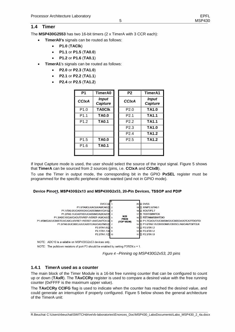
The MSP430G2553 has two 16-bit timers (2 x TimerA with 3 CCR each):
TimerA0's signals can be routed as follows:
P1.0 (TAClk)
P1.1 or P1.5 (TA0.0)
P1.2 or P1.6 (TA0.1)
TimerA1's signals can be routed as follows:
P2.0 or P2.3 (TA1.0)
P2.1 or P2.2 (TA1.1)
P2.4 or P2.5 (TA1.2)
P1 TimerA0 P2 TimerA1
CCIxA Input
Capture CCIxA
Input Capture
P1.0 TA0Clk P2.0 TA1.0
P1.1 TA0.0 P2.1 TA1.1
P1.2 TA0.1 P2.2 TA1.1
P2.3 TA1.0
P2.4 TA1.2
P1.5 TA0.0 P2.5 TA1.2
P1.6 TA0.1
If Input Capture mode is used, the user should select the source of the input signal. Figure 5 shows that TimerA can be sourced from 2 sources (pins, i.e. CCIxA and CCIxB).
To use the Timer in output mode, the corresponding bit in the GPIO PxSEL register must be programmed for the specific peripheral mode wanted (and not in GPIO mode).
Figure 4 –Pinning og MSP430G2x53, 20 pins
1.4.1 TimerA used as a counter
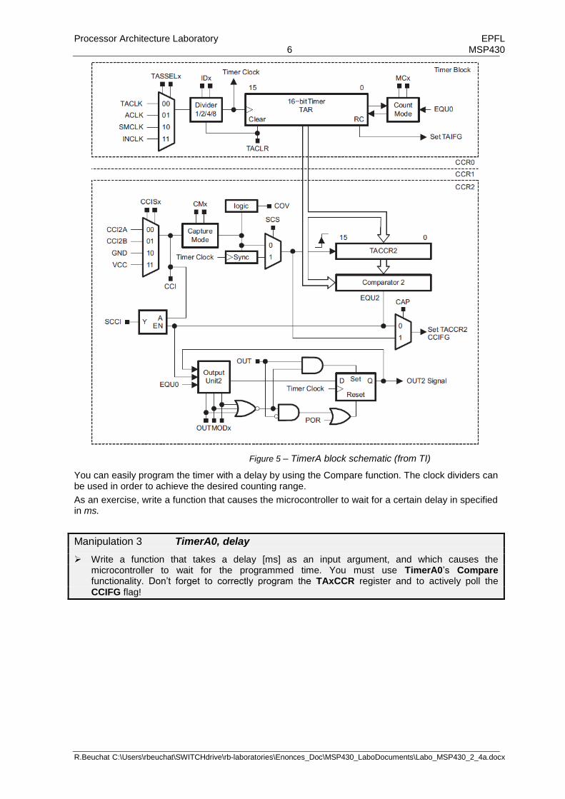
The main block of the Timer Module is a 16-bit free running counter that can be configured to count up or down (TAxR). The TAxCCRy register is used to compare a desired value with the free running counter (0xFFFF is the maximum upper value).
The TAxCCRy CCIFG flag is used to indicate when the counter has reached the desired value, and could generate an interruption if properly configured. Figure 5 below shows the general architecture of the TimerA unit:
Processor Architecture Laboratory EPFL 6 MSP430
R.Beuchat C:\Users\rbeuchat\SWITCHdrive\rb-laboratories\Enonces_Doc\MSP430_LaboDocuments\Labo_MSP430_2_4a.docx
Figure 5 – TimerA block schematic (from TI)
You can easily program the timer with a delay by using the Compare function. The clock dividers can be used in order to achieve the desired counting range.
As an exercise, write a function that causes the microcontroller to wait for a certain delay in specified in ms.
Manipulation 3 TimerA0, delay
Write a function that takes a delay [ms] as an input argument, and which causes the microcontroller to wait for the programmed time. You must use TimerA0’s Compare functionality. Don’t forget to correctly program the TAxCCR register and to actively poll the CCIFG flag!

Processor Architecture Laboratory EPFL 7 MSP430
R.Beuchat C:\Users\rbeuchat\SWITCHdrive\rb-laboratories\Enonces_Doc\MSP430_LaboDocuments\Labo_MSP430_2_4a.docx
1.4.2 PWM generation
Use TimerA0 to generate a periodic pulse through pulse width modulation (PWM mode).
Write a function that generates a pulse with a period of ~10 [ms]. The pulse’s duty cycle should be programmed as the function’s parameter. Study the different modes available on TimerA to generate the PWM pulse.
You can find a block diagram of TimerA in Figure 5 above.
Manipulation 4 PWM with TimerA
Use TimerA0 to generate a PWM pulse by configuring the CCR comparator to operate in the proper manner. The PWM pulse must have a period of ~10[ms]. Use an oscilloscope to view and validate the results.
1.5 TimerA0 interrupt-generation
It is possible to use TimerA0 in Output compare mode to generate a periodic interrupt. A vector table contains the address of every interrupt routine that needs to be called for a specific Interrupt Request.
As an example, we can study the vector table for the MSP430F5437 microprocessor (not the one used in this laboratory!), which can be found in the header file for this specific microcontroller: msp430f5437.h.
We can see that the vector table starts at address 0xFF80, and each entry is 16 bits wide. The address for TimerA0’s interrupt routing is 0xFFEC (entry 54 in decimal, so 0xFF80 + 2*54 = 0xFFEC)).
A specific compiler pragma is used by the compiler to specify the interrupt service routine and the corresponding vector address.
#define TIMER0_B0_VECTOR (60 * 1u) /* 0xFFF8 Timer0_B7 CC0 */
#define TIMER0_B1_VECTOR (59 * 1u) /* 0xFFF6 Timer0_B7 CC1-6, TB */
#define TIMER0_A0_VECTOR (54 * 1u) /* 0xFFEC Timer0_A5 CC0 */
#define TIMER0_A1_VECTOR (53 * 1u) /* 0xFFEA Timer0_A5 CC1-4, TA0
*/
#define TIMER1_A0_VECTOR (49 * 1u) /* 0xFFE2 Timer1_A3 CC0 */
#define TIMER1_A1_VECTOR (48 * 1u) /* 0xFFE0 Timer1_A3 CC1-2, TA1
*/
Below, you will find a code segment that specifies and interrupt routine in Code Composer 6:
#pragma vector=TIMER0_A1_VECTOR
__interrupt void TimerA0(void) // Interrupt routine for TAIFG
{
// something to do…
TA0CTL &= (~TAIFG); // Clear TAIFG flag in TA0CTL register
}
In order to enable global interrupts, the following instruction must be executed:
__bis_SR_register(GIE); // Enable global Interrupt
Manipulation 5 Interruption on TimerA0
Use TimerA0 to generate periodic interrupts every ~50ms. Toggle a GPIO pin on each interrupt.
Use an oscilloscope to view and validate the results.
Processor Architecture Laboratory EPFL 8 MSP430
R.Beuchat C:\Users\rbeuchat\SWITCHdrive\rb-laboratories\Enonces_Doc\MSP430_LaboDocuments\Labo_MSP430_2_4a.docx
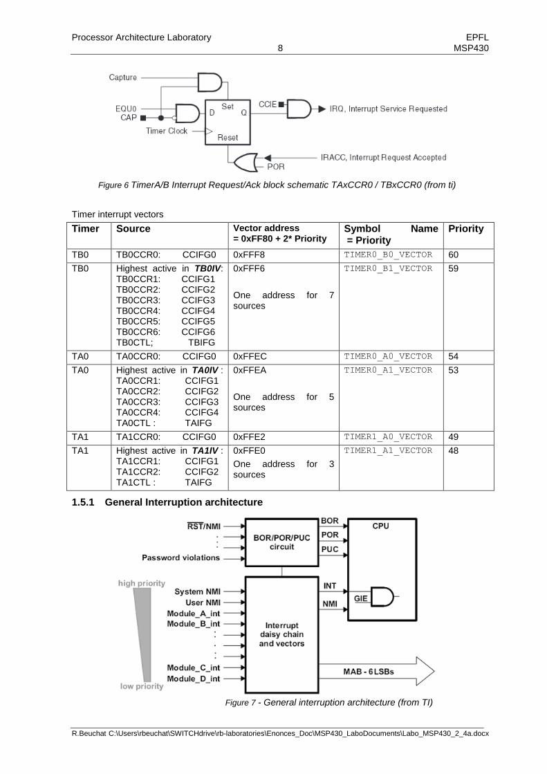
Figure 6 TimerA/B Interrupt Request/Ack block schematic TAxCCR0 / TBxCCR0 (from ti)
Timer interrupt vectors
Timer Source Vector address = 0xFF80 + 2* Priority
Symbol Name = Priority
Priority
TB0 TB0CCR0: CCIFG0 0xFFF8 TIMER0_B0_VECTOR 60
TB0 Highest active in TB0IV: TB0CCR1: CCIFG1 TB0CCR2: CCIFG2 TB0CCR3: CCIFG3 TB0CCR4: CCIFG4 TB0CCR5: CCIFG5 TB0CCR6: CCIFG6 TB0CTL; TBIFG
0xFFF6
One address for 7 sources
TIMER0_B1_VECTOR 59
TA0 TA0CCR0: CCIFG0 0xFFEC TIMER0_A0_VECTOR 54
TA0 Highest active in TA0IV : TA0CCR1: CCIFG1 TA0CCR2: CCIFG2 TA0CCR3: CCIFG3 TA0CCR4: CCIFG4 TA0CTL : TAIFG
0xFFEA
One address for 5 sources
TIMER0_A1_VECTOR 53
TA1 TA1CCR0: CCIFG0 0xFFE2 TIMER1_A0_VECTOR 49
TA1 Highest active in TA1IV : TA1CCR1: CCIFG1 TA1CCR2: CCIFG2 TA1CTL : TAIFG
0xFFE0
One address for 3 sources
TIMER1_A1_VECTOR 48
1.5.1 General Interruption architecture
Figure 7 - General interruption architecture (from TI)

Processor Architecture Laboratory EPFL 9 MSP430
R.Beuchat C:\Users\rbeuchat\SWITCHdrive\rb-laboratories\Enonces_Doc\MSP430_LaboDocuments\Labo_MSP430_2_4a.docx
1.5.2 General Interruption architecture
Figure 8 - General interrupt architecture (fromTI)
(1) Multiple source flags
(2) A reset is generated if the CPU tries to fetch instructions from within peripheral space or vacant memory space.
(Non)maskable: the individual interrupt-enable bit can disable an interrupt event, but the general-interrupt enable cannot disable it.
(3) Interrupt flags are located in the module.
(4) Reserved interrupt vectors at addresses are not used in this device and can be used for regular program code if necessary. To maintain compatibility with other devices, it is recommended to reserve these locations.

Processor Architecture Laboratory EPFL 10 MSP430
R.Beuchat C:\Users\rbeuchat\SWITCHdrive\rb-laboratories\Enonces_Doc\MSP430_LaboDocuments\Labo_MSP430_2_4a.docx
1.6 ADC
The MSP430G2553 supports 10-bit analog-to-digital conversion. The programmable module responsible for this is referred to as the ADC10 peripheral. Its block diagram is depicted below.
Figure 9 – ADC10 bloc diagram (fromTI)
It basically works as follows:
Pins can be configured as analog inputs to the ADC10. Using the P1SEL register, as specified by the datasheet, one can map P1.7..P1.0 to A7..A0, respectively.
The inputs can be selected using the INCHx bits of the ADC10CTL1 register (again, make sure to check the ADC10 Registers section of the user manual).
At the rising edge of the SHI signal, a sampling stage will be initiated. Then, depending on how the Sample Timer is configured by the programmer (i.e. you), the SAMPCON signal is
Processor Architecture Laboratory EPFL 11 MSP430
R.Beuchat C:\Users\rbeuchat\SWITCHdrive\rb-laboratories\Enonces_Doc\MSP430_LaboDocuments\Labo_MSP430_2_4a.docx
held high during a certain period (in function of the period of SHI). The SAMPCON signal determines how long the analog signal must be sampled.
As soon as SAMPCON goes low, the conversion stage is initiated and will last 13 ADC10CLK cycles.
Finally, the sampled value will be available in the ADC10MEM register.
Now it is your turn to have fun configuring all these registers, and don’t forget to read the documentation ;) !
Manipulation 6 ADC, Analog to Digital Converter
Write a function that use the ADC10 module to acquire an analog signal obtained from an external potentiometer. To plug in the potentiometer, refer to figure and the explanations provided in the next section.
1.6.1 ADC to control PWM
The goal of this section is to use the sampled value obtained from the ADC10 to control the duty cycle of your PWM. The A/D converter should be read every ~50ms. Use interrupts to meet this timing requirement.
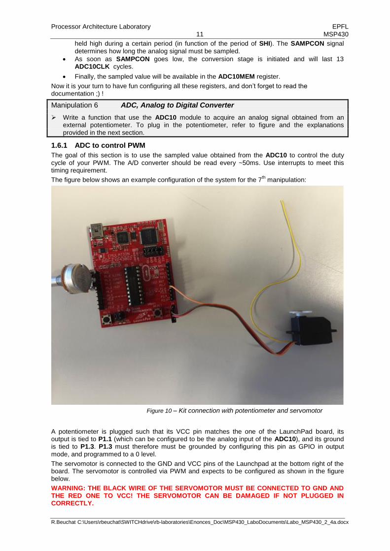
The figure below shows an example configuration of the system for the 7th manipulation:
Figure 10 – Kit connection with potentiometer and servomotor
A potentiometer is plugged such that its VCC pin matches the one of the LaunchPad board, its output is tied to P1.1 (which can be configured to be the analog input of the ADC10), and its ground is tied to P1.3. P1.3 must therefore must be grounded by configuring this pin as GPIO in output mode, and programmed to a 0 level.
The servomotor is connected to the GND and VCC pins of the Launchpad at the bottom right of the board. The servomotor is controlled via PWM and expects to be configured as shown in the figure below.
WARNING: THE BLACK WIRE OF THE SERVOMOTOR MUST BE CONNECTED TO GND AND THE RED ONE TO VCC! THE SERVOMOTOR CAN BE DAMAGED IF NOT PLUGGED IN CORRECTLY.

Processor Architecture Laboratory EPFL 12 MSP430
R.Beuchat C:\Users\rbeuchat\SWITCHdrive\rb-laboratories\Enonces_Doc\MSP430_LaboDocuments\Labo_MSP430_2_4a.docx
The orange wire is the input of the servomotor and should be tied to a pin that outputs the PWM generated by your timer.
Figure 11 – PWM Pulse Width Modulation timing
Manipulation 7 Timer, ADC, PWM, GPIO and interrupts
Use a timer interrupt to periodically enable the ADC converter in software and to start a conversion of the potentiometer value.
Use another interrupt from the (ADC10 module this time) to catch the sampled value and use it to adjust the duty cycle of the pulses your pulse-width modulator generates.
Make a demo to an assistant where you can visualize the result with an oscilloscope/logic analyzer and the servomotor.
Extra: try to avoid the use of a software routine to enable the ADC conversion process, but instead connect the timer directly to the ADC10 (find out where to perform the connection from the ADC10 bloc diagram above).