msp430fr697x(1), msp430fr687x(1), msp430fr692x… · 4 msp430fr6972, msp430fr69721, msp430fr6970,...
TRANSCRIPT
Product
Folder
Order
Now
Technical
Documents
Tools &
Software
Support &Community
ReferenceDesign
An IMPORTANT NOTICE at the end of this data sheet addresses availability, warranty, changes, use in safety-critical applications,intellectual property matters and other important disclaimers. PRODUCTION DATA.
MSP430FR6972, MSP430FR69721, MSP430FR6970, MSP430FR6872MSP430FR68721, MSP430FR6870, MSP430FR6922, MSP430FR69221MSP430FR6920, MSP430FR6822, MSP430FR68221, MSP430FR6820
SLASE23D –JANUARY 2015–REVISED JANUARY 2017
MSP430FR697x(1), MSP430FR687x(1), MSP430FR692x(1), MSP430FR682x(1)Mixed‑‑Signal Microcontrollers
1 Device Overview
1
1.1 Features1
(1) Minimum supply voltage is restricted by SVS levels.(2) The RTC is clocked by a 3.7-pF crystal.
• Embedded Microcontroller– 16-Bit RISC Architecture up to 16-MHz Clock– Wide Supply Voltage Range (1.8 V to 3.6 V) (1)
• Optimized Ultra-Low-Power Modes– Active Mode: Approximately 100 µA/MHz– Standby (LPM3 With VLO): 0.4 µA (Typical)– Real-Time Clock (RTC) (LPM3.5):
0.35 µA (Typical) (2)
– Shutdown (LPM4.5): 0.04 µA (Typical)• Ultra-Low-Power Ferroelectric RAM (FRAM)
– Up to 64KB of Nonvolatile Memory– Ultra-Low-Power Writes– Fast Write at 125 ns per Word (64KB in 4 ms)– Unified Memory = Program, Data, and Storage
in One Single Space– 1015 Write Cycle Endurance– Radiation Resistant and Nonmagnetic
• Intelligent Digital Peripherals– 32-Bit Hardware Multiplier (MPY)– Three-Channel Internal Direct Memory Access
(DMA)– RTC With Calendar and Alarm Functions– Five 16-Bit Timers With up to Seven
Capture/Compare Registers– 16-Bit and 32-Bit Cyclic Redundancy Checker
(CRC16, CRC32)• High-Performance Analog
– Up to 8-Channel Analog Comparator– 12-Bit Analog-to-Digital Converter (ADC) With
Internal Reference and Sample-and-Hold andup to 8 External Input Channels
– Integrated 116-Segment LCD Driver WithContrast Control
• Code Security and Encryption– 128-Bit or 256-Bit AES Security Encryption and
Decryption Coprocessor (MSP430FR69xx(1)Only)
– True Random Number Seed for RandomNumber Generation Algorithm
– Lockable Memory Segments for IPEncapsulation and Secure Storage
• Multifunction Input/Output Ports– All I/O Pins Support Capacitive Touch Capability
Without Need for External Components– Accessible Bit-, Byte- and Word-Wise (in Pairs)– Edge-Selectable Wakeup From LPM on Ports
P1 to P4– Programmable Pullup and Pulldown on All Ports
• Enhanced Serial Communication– eUSCI_A0 and eUSCI_A1 Support:
– UART With Automatic Baud-Rate Detection– IrDA Encode and Decode– SPI at Rates up to 10 Mbps
– eUSCI_B0 and eUSCI_B1 Support:– I2C With Multiple-Slave Addressing– SPI at Rates up to 10 Mbps
• Flexible Clock System– Fixed-Frequency DCO With 10 Selectable
Factory-Trimmed Frequencies– Low-Power Low-Frequency Internal Clock
Source (VLO)– 32-kHz Crystals (LFXT)– High-Frequency Crystals (HFXT)
• Development Tools and Software– Free Professional Development Environments
With EnergyTrace++™ Technology for PowerProfiling and Debugging
– Microcontroller Development Boards Available• Family Members
– Section 3 Summarizes the Available Variantsand Packages
• For Complete Module Descriptions, See theMSP430FR58xx, MSP430FR59xx,MSP430FR68xx, and MSP430FR69xx FamilyUser's Guide

2
MSP430FR6972, MSP430FR69721, MSP430FR6970, MSP430FR6872MSP430FR68721, MSP430FR6870, MSP430FR6922, MSP430FR69221MSP430FR6920, MSP430FR6822, MSP430FR68221, MSP430FR6820SLASE23D –JANUARY 2015–REVISED JANUARY 2017 www.ti.com
Submit Documentation FeedbackProduct Folder Links: MSP430FR6972 MSP430FR69721 MSP430FR6970 MSP430FR6872 MSP430FR68721
MSP430FR6870 MSP430FR6922 MSP430FR69221 MSP430FR6920 MSP430FR6822 MSP430FR68221MSP430FR6820
Device Overview Copyright © 2015–2017, Texas Instruments Incorporated
1.2 Applications• Heat Cost Allocators• Utility Meters – Electricity, Water, and Gas• Thermostats
• Portable Medical Equipment• Sensor Management• Weigh Scales
1.3 DescriptionThis ultra-low-power MSP430FRxx FRAM microcontroller family consists of several devices featuringembedded nonvolatile FRAM, a 16-bit CPU, and different sets of peripherals targeted for variousapplications. The architecture, FRAM, and peripherals, combined with seven low-power modes, areoptimized to achieve extended battery life in portable and wireless sensing applications. FRAM is a newnonvolatile memory that combines the speed, flexibility, and endurance of SRAM with the stability andreliability of flash, all at lower total power consumption.
(1) For the most current part, package, and ordering information for all available devices, see the PackageOption Addendum in Section 9, or see the TI website at www.ti.com.
(2) The sizes shown here are approximations. For the package dimensions with tolerances, see theMechanical Data in Section 9.
Device Information (1)
PART NUMBER PACKAGE BODY SIZE (2)
MSP430FR6972IPMR LQFP (64) 10 mm × 10 mmMSP430FR6972IRGC VQFN (64) 9 mm × 9 mmMSP430FR6922IG56 TSSOP (56) 6.1 mm × 14 mm

EEM
(S: 3+1)
Comp_E
(up to 16inputs)
FRAM
64KB32KB
RAM
2KB
PowerMgmt
LDOSVS
Brownout
SMCLK
ACLK
MDB
MAB
HFXOUTHFXIN
Spy-Bi-
Wire
CRC32
CRC-32-ISO-3309
CRC16
CRC-16-CCITT
BusControlLogic
MAB
MDB
MAB
MDB
MCLK
MPY32
AES256
SecurityEn-/De-cryption
(128/256)
ADC12_B
(up to 16std. inputs,
up to 8diff. inputs)
ClockSystem
CPUXV2incl. 16
Registers
JTAG
Interface
DMA
Controller
3 Channel
REF_A
VoltageReference
MPUIP Encap
TB0
Timer_B7 CC
Registers(int./ext.)
TA0
Timer_A3 CC
Registers(int./ext.)
TA1
Timer_A3 CC
Registers(int./ext.)
RTC_C
Calendarand
CounterMode
LCD_C
(up to116 seg;
static,2 to 4 mux)
eUSCI_A0eUSCI_A1
(UART,IrDA,SPI)
eUSCI_B0eUSCI_B1
(I C,SPI)
2
LPM3.5 Domain
P1.x,P2.x
I/O PortP5, P6
2x8 I/Os
PC1x16 I/Os
I/O PortP7
1x8 I/Os
PD1x8 I/Os
I/O PortP9
1x8 I/Os
PE1x8 I/Os
I/O PortPJ
1x8 I/Os
I/O PortsP3, P4
2x8 I/Os
PB1x16 I/Os
I/O PortsP1, P2
2x8 I/Os
PA1x16 I/Os
P9.x
up to1x8
PJ.x
Watchdog
TA2
Timer_A2 CC
Registers(int. only)
TA 3
Timer_A5 CC
Registers
Capacitive Touch IO 0, Capacitive Touch IO 1
P7.x
up to1x8
up to1x8
up to2x8
up to2x8
up to2x8
P3.x,P4.x P5.x,P6.x
LFXOUT,LFXIN,
Tiny RAM26B
Copyright © 2016, Texas Instruments Incorporated
3
MSP430FR6972, MSP430FR69721, MSP430FR6970, MSP430FR6872MSP430FR68721, MSP430FR6870, MSP430FR6922, MSP430FR69221MSP430FR6920, MSP430FR6822, MSP430FR68221, MSP430FR6820
www.ti.com SLASE23D –JANUARY 2015–REVISED JANUARY 2017
Submit Documentation FeedbackProduct Folder Links: MSP430FR6972 MSP430FR69721 MSP430FR6970 MSP430FR6872 MSP430FR68721
MSP430FR6870 MSP430FR6922 MSP430FR69221 MSP430FR6920 MSP430FR6822 MSP430FR68221MSP430FR6820
Device OverviewCopyright © 2015–2017, Texas Instruments Incorporated
1.4 Functional Block DiagramFigure 1-1 shows the functional block diagram.
NOTE: AES256 is not implemented in the MSP430FR682x, MSP430FR687x, MSP430FR682x1, and MSP430FR687x1devices.
NOTE: HFXIN and HFOUT are not implemented in the MSP430FR692x, MSP430FR682x, MSP430FR692x1, andMSP430FR682x1 devices.
Figure 1-1. Functional Block Diagram

4
MSP430FR6972, MSP430FR69721, MSP430FR6970, MSP430FR6872MSP430FR68721, MSP430FR6870, MSP430FR6922, MSP430FR69221MSP430FR6920, MSP430FR6822, MSP430FR68221, MSP430FR6820SLASE23D –JANUARY 2015–REVISED JANUARY 2017 www.ti.com
Submit Documentation FeedbackProduct Folder Links: MSP430FR6972 MSP430FR69721 MSP430FR6970 MSP430FR6872 MSP430FR68721
MSP430FR6870 MSP430FR6922 MSP430FR69221 MSP430FR6920 MSP430FR6822 MSP430FR68221MSP430FR6820
Table of Contents Copyright © 2015–2017, Texas Instruments Incorporated
Table of Contents1 Device Overview ......................................... 1
1.1 Features .............................................. 11.2 Applications........................................... 21.3 Description............................................ 21.4 Functional Block Diagram ............................ 3
2 Revision History ......................................... 53 Device Comparison ..................................... 6
3.1 Related Products ..................................... 84 Terminal Configuration and Functions.............. 9
4.1 Pin Diagrams ......................................... 94.2 Pin Attributes ........................................ 124.3 Signal Descriptions.................................. 184.4 Pin Multiplexing ..................................... 264.5 Buffer Type.......................................... 264.6 Connection of Unused Pins ......................... 26
5 Specifications ........................................... 275.1 Absolute Maximum Ratings ......................... 275.2 ESD Ratings ........................................ 275.3 Recommended Operating Conditions............... 275.4 Active Mode Supply Current Into VCC Excluding
External Current .................................... 285.5 Typical Characteristics - Active Mode Supply
Currents ............................................. 295.6 Low-Power Mode (LPM0, LPM1) Supply Currents
Into VCC Excluding External Current ................ 295.7 Low-Power Mode LPM2, LPM3, LPM4 Supply
Currents (Into VCC) Excluding External Current .... 305.8 Low-Power Mode With LCD Supply Currents (Into
VCC) Excluding External Current .................... 325.9 Low-Power Mode LPMx.5 Supply Currents (Into
VCC) Excluding External Current .................... 335.10 Typical Characteristics, Low-Power Mode Supply
Currents ............................................. 345.11 Typical Characteristics, Current Consumption per
Module .............................................. 355.12 Thermal Resistance Characteristics ................ 35
5.13 Timing and Switching Characteristics ............... 366 Detailed Description ................................... 65
6.1 Overview ............................................ 656.2 CPU ................................................. 656.3 Operating Modes .................................... 666.4 Interrupt Vector Table and Signatures .............. 686.5 Bootloader (BSL).................................... 716.6 JTAG Operation ..................................... 716.7 FRAM................................................ 726.8 RAM ................................................. 726.9 Tiny RAM............................................ 726.10 Memory Protection Unit (MPU) Including IP
Encapsulation ....................................... 726.11 Peripherals .......................................... 736.12 Device Descriptors (TLV) .......................... 1106.13 Memory ............................................ 1136.14 Identification........................................ 129
7 Applications, Implementation, and Layout ...... 1307.1 Device Connection and Layout Fundamentals .... 1307.2 Peripheral- and Interface-Specific Design
Information ......................................... 1348 Device and Documentation Support .............. 137
8.1 Getting Started and Next Steps ................... 1378.2 Device Nomenclature .............................. 1378.3 Tools and Software ................................ 1398.4 Documentation Support............................ 1418.5 Related Links ...................................... 1428.6 Community Resources............................. 1428.7 Trademarks ........................................ 1438.8 Electrostatic Discharge Caution ................... 1438.9 Export Control Notice .............................. 1438.10 Glossary............................................ 143
9 Mechanical, Packaging, and OrderableInformation ............................................. 144

5
MSP430FR6972, MSP430FR69721, MSP430FR6970, MSP430FR6872MSP430FR68721, MSP430FR6870, MSP430FR6922, MSP430FR69221MSP430FR6920, MSP430FR6822, MSP430FR68221, MSP430FR6820
www.ti.com SLASE23D –JANUARY 2015–REVISED JANUARY 2017
Submit Documentation FeedbackProduct Folder Links: MSP430FR6972 MSP430FR69721 MSP430FR6970 MSP430FR6872 MSP430FR68721
MSP430FR6870 MSP430FR6922 MSP430FR69221 MSP430FR6920 MSP430FR6822 MSP430FR68221MSP430FR6820
Revision HistoryCopyright © 2015–2017, Texas Instruments Incorporated
2 Revision HistoryNOTE: Page numbers for previous revisions may differ from page numbers in the current version.
Changes from April 28, 2015 to January 24, 2017 Page
• Removed 48KB FRAM option from Figure 1-1, Functional Block Diagram ................................................... 3• Added Section 3.1, Related Products ............................................................................................. 8• Added ACLK as additional signal multiplexed on P7.1 pin in Figure 4-1...................................................... 9• Added note that starts "TI recommends connecting..." to Figure 4-1, 64-Pin PM and RGC Packages (Top View),
MSP430FR692x(1) MSP430FR682x(1) ........................................................................................... 9• Added ACLK as additional signal multiplexed on P7.1 pin in Figure 4-2 .................................................... 10• Added note that starts "TI recommends connecting..." to Figure 4-2, 64-Pin PM and RGC Packages (Top
View) – MSP430FR697x(1), MSP430FR687x(1) ............................................................................... 10• Added ACLK as additional signal multiplexed on P7.1 pin in Figure 4-3 .................................................... 11• Changed definition of OFF reset state ........................................................................................... 12• Added ACLK as additional signal multiplexed on P7.1 pin in Table 4-1 ..................................................... 15• Added additional pin numbers where ACLK signal is available in Table 4-2................................................ 18• Added row for VQFN thermal pad ................................................................................................ 25• Removed NOM value and added MIN value for the CDVCC parameter in Section 5.3, Recommended Operating
Conditions ............................................................................................................................ 27• Added oscillation allowance parameter (OAHFXT) in Table 5-5, High-Frequency Crystal Oscillator, HFXT ............. 39• Removed ADC12DIV from the formula on the tCONVERT parameter TYP value, because ADC12CLK is after division 57• Added second row to tSample parameter in Table 5-25, 12-Bit ADC, Timing Parameters .................................. 58• Added "RS < 10 kΩ" to the note that starts "Approximately 10 Tau (τ) are needed..." on Table 5-25, 12-Bit ADC,
Timing Parameters .................................................................................................................. 58• Changed the note that starts "Tools that access the Spy-Bi-Wire and BSL interfaces..." ................................. 64• Added Section 6.3.1, Peripherals in Low-Power Modes ....................................................................... 67• Changed all instances of "bootstrap loader" to "bootloader" .................................................................. 71• Added Table 6-18, LCD Automatic Charge Pump Disable Bits (LCDCPDISx) ............................................ 82• Added ACLK to P7.1 in PIN NAME column of Table 6-29..................................................................... 98• Changed from "If the RST/NMI pin is unused...with a 2.2-nF pulldown capacitor" to "If the RST/NMI pin is
unused...with a 10-nF pulldown capacitor" in Section 7.1.4, Reset ......................................................... 133• Replaced former section Development Tools Support with Section 8.3, Tools and Software .......................... 139• Added content to Section 8.4, Documentation Support ...................................................................... 141

Copyright © 2015–2017, Texas Instruments IncorporatedDevice ComparisonSubmit Documentation Feedback
Product Folder Links: MSP430FR6972 MSP430FR69721 MSP430FR6970 MSP430FR6872 MSP430FR68721MSP430FR6870 MSP430FR6922 MSP430FR69221 MSP430FR6920 MSP430FR6822 MSP430FR68221
MSP430FR6820
6
MSP430FR6972, MSP430FR69721, MSP430FR6970, MSP430FR6872MSP430FR68721, MSP430FR6870, MSP430FR6922, MSP430FR69221MSP430FR6920, MSP430FR6822, MSP430FR68221, MSP430FR6820SLASE23D –JANUARY 2015–REVISED JANUARY 2017 www.ti.com
3 Device Comparison
Table 3-1 and Table 3-2 summarize the available family members.
(1) Each number in the sequence represents an instantiation of Timer_A with its associated number of capture compare registers and PWM output generators available. For example, anumber sequence of 3, 5 would represent two instantiations of Timer_A, the first instantiation having 3 and the second instantiation having 5 capture compare registers and PWM outputgenerators, respectively.
(2) Each number in the sequence represents an instantiation of Timer_B with its associated number of capture compare registers and PWM output generators available. For example, anumber sequence of 3, 5 would represent two instantiations of Timer_B, the first instantiation having 3 and the second instantiation having 5 capture compare registers and PWM outputgenerators, respectively.
(3) eUSCI_A supports UART with automatic baud-rate detection, IrDA encode and decode, and SPI.(4) eUSCI_B supports I2C with multiple slave addresses and SPI.(5) Timer_A TA0 and TA1 provide internal and external capture/compare inputs and internal and external PWM outputs.(6) Timer_A TA2 provides only internal capture/compare inputs and only internal PWM outputs (if any).(7) Timer_A TA3 provides only internal capture/compare inputs and only internal PWM outputs (if any) for FR692x(1) and FR682x(1) with RGC and PM packages. For FR692x(1) and
FR682x(1) with DGG package and all other devices, Timer_A TA3 provides internal, external capture/compare inputs and internal, external PWM outputs (if any).
Table 3-1. Device Comparison – Family Members With UART BSL
DEVICE FRAM(KB)
SRAM(KB)
CLOCKSYSTEM Timer_A (1) Timer_B (2) eUSCI
AES ADC12_B LCD_C I/O PACKAGEA (3) B (4)
MSP430FR6972 64 2DCOHFXTLFXT
3, 3 (5)
2, 5 (6) (7) 7 2 2 yes 8 ext 112 seg 51 64 PM64 RGC
MSP430FR6872 64 2DCOHFXTLFXT
3, 3 (5)
2, 5 (6) (7) 7 2 2 no 8 ext 112 seg 51 64 PM64 RGC
MSP430FR6970 32 2DCOHFXTLFXT
3, 3 (5)
2, 5 (6) (7) 7 2 2 yes 8 ext 112 seg 51 64 PM64 RGC
MSP430FR6870 32 2DCOHFXTLFXT
3, 3 (5)
2, 5 (6) (7) 7 2 2 no 8 ext 112 seg 51 64 PM64 RGC
MSP430FR6922 64 2 DCOLFXT
3, 3 (5)
2, 5 (6) (7) 7 2 2 yes 8 ext116 seg100 seg(DGG)
5246 (DGG)
64 PM64 RGC56 DGG
MSP430FR6822 64 2 DCOLFXT
3, 3 (5)
2, 5 (6) (7) 7 2 2 no 8 ext116 seg100 seg(DGG)
5246 (DGG)
64 PM64 RGC56 DGG
MSP430FR6920 32 2 DCOLFXT
3, 3 (5)
2, 5 (6) (7) 7 2 2 yes 8 ext116 seg100 seg(DGG)
5246 (DGG)
64 PM64 RGC56 DGG
MSP430FR6820 32 2 DCOLFXT
3, 3 (5)
2, 5 (6) (7) 7 2 2 no 8 ext116 seg100 seg(DGG)
5246 (DGG)
64 PM64 RGC56 DGG

Copyright © 2015–2017, Texas Instruments Incorporated Device ComparisonSubmit Documentation Feedback
Product Folder Links: MSP430FR6972 MSP430FR69721 MSP430FR6970 MSP430FR6872 MSP430FR68721MSP430FR6870 MSP430FR6922 MSP430FR69221 MSP430FR6920 MSP430FR6822 MSP430FR68221
MSP430FR6820
7
MSP430FR6972, MSP430FR69721, MSP430FR6970, MSP430FR6872MSP430FR68721, MSP430FR6870, MSP430FR6922, MSP430FR69221MSP430FR6920, MSP430FR6822, MSP430FR68221, MSP430FR6820
www.ti.com SLASE23D –JANUARY 2015–REVISED JANUARY 2017
(1) Each number in the sequence represents an instantiation of Timer_A with its associated number of capture compare registers and PWM output generators available. For example, anumber sequence of 3, 5 would represent two instantiations of Timer_A, the first instantiation having 3 and the second instantiation having 5 capture compare registers and PWM outputgenerators, respectively.
(2) Each number in the sequence represents an instantiation of Timer_B with its associated number of capture compare registers and PWM output generators available. For example, anumber sequence of 3, 5 would represent two instantiations of Timer_B, the first instantiation having 3 and the second instantiation having 5 capture compare registers and PWM outputgenerators, respectively.
(3) eUSCI_A supports UART with automatic baud-rate detection, IrDA encode and decode, and SPI.(4) eUSCI_B supports I2C with multiple slave addresses and SPI.(5) Timer_A TA0 and TA1 provide internal and external capture/compare inputs and internal and external PWM outputs.(6) Timer_A TA2 provides only internal capture/compare inputs and only internal PWM outputs (if any).(7) Timer_A TA3 provides only internal capture/compare inputs and only internal PWM outputs (if any) for FR692x(1) and FR682x(1) with RGC and PM packages. For FR692x(1) and
FR682x(1) with DGG package and all other devices, Timer_A TA3 provides internal, external capture/compare inputs and internal, external PWM outputs (if any).
Table 3-2. Device Comparison – Family Members With I2C BSL
DEVICE FRAM(KB)
SRAM(KB)
CLOCKSYSTEM Timer_A (1) Timer_B (2) eUSCI
AES ADC12_B LCD_C I/O PACKAGEA (3) B (4)
MSP430FR69721 64 2DCOHFXTLFXT
3, 3 (5)
2, 5 (6) (7) 7 2 2 yes 8 ext 112 seg 51 64 PM64 RGC
MSP430FR68721 64 2DCOHFXTLFXT
3, 3 (5)
2, 5 (6) (7) 7 2 2 no 8 ext 112 seg 51 64 PM64 RGC
MSP430FR69221 64 2 DCOLFXT
3, 3 (5)
2, 5 (6) (7) 7 2 2 yes 8 ext116 seg100 seg(DGG)
5246 (DGG)
64 PM64 RGC56 DGG
MSP430FR68221 64 2 DCOLFXT
3, 3 (5)
2, 5 (6) (7) 7 2 2 no 8 ext116 seg100 seg(DGG)
5246 (DGG)
64 PM64 RGC56 DGG

8
MSP430FR6972, MSP430FR69721, MSP430FR6970, MSP430FR6872MSP430FR68721, MSP430FR6870, MSP430FR6922, MSP430FR69221MSP430FR6920, MSP430FR6822, MSP430FR68221, MSP430FR6820SLASE23D –JANUARY 2015–REVISED JANUARY 2017 www.ti.com
Submit Documentation FeedbackProduct Folder Links: MSP430FR6972 MSP430FR69721 MSP430FR6970 MSP430FR6872 MSP430FR68721
MSP430FR6870 MSP430FR6922 MSP430FR69221 MSP430FR6920 MSP430FR6822 MSP430FR68221MSP430FR6820
Device Comparison Copyright © 2015–2017, Texas Instruments Incorporated
3.1 Related ProductsFor information about other devices in this family of products or related products, see the following links.Products for TI Microcontrollers TI's low-power and high-performance MCUs, with wired and wireless
connectivity options, are optimized for a broad range of applications.Products for MSP430 Ultra-Low-Power Microcontrollers One platform. One ecosystem. Endless
possibilities. — Enabling the connected world with innovations in ultra-low-powermicrocontrollers with advanced peripherals for precise sensing and measurement.
Products for MSP430FRxx FRAM Microcontrollers MSP430F5x/6x microcontrollers from the MSP low-power and performance MCU series offer low power with added performance and increaseddesign options. These 16-bit devices feature new and innovative integrated peripherals suchas USB and LCD on chip, in addition to higher CPU speeds and more memory.
Companion Products for MSP430FR6972 Review products that are frequently purchased or used withthis product.
Reference Designs for MSP430FR6972 The TI Designs Reference Design Library is a robust referencedesign library that spans analog, embedded processor, and connectivity. Created by TIexperts to help you jump start your system design, all TI Designs include schematic or blockdiagrams, BOMs, and design files to speed your time to market. Search and downloaddesigns at ti.com/tidesigns.

1P4.3/UCA0SOMI/UCA0RXD/UCB1STE
2P1.4/UCB0CLK/UCA0STE/TA1.0/S3
3P1.5/UCB0STE/UCA0CLK/TA0.0/S2
4P1.6/ TA0.1/S1UCB0SIMO/UCB0SDA/
5P1.7/ TA0.2/S0UCB0SOMI/UCB0SCL/
6R33/LCDCAP
7P6.0/R23
8P6.1/R13/LCDREF
9P6.2/COUT/R03
10P6.3/COM0
11P6.4/TB0.0/COM1/S31
12P6.5/TB0.1/COM2/S30
13P6.6/TB0.2/COM3/S29
14P3.0/UCB1CLK/S28
15P3.1/ S27UCB1SIMO/UCB1SDA/
16P3.2/ S26UCB1SOMI/UCB1SCL/
17
DV
SS
1
18
DV
CC
1
19
TE
ST
/SB
WT
CK
20
RS
T/N
MI/S
BW
TD
IO
21
PJ.0
/TD
O/T
B0O
UT
H/S
MC
LK
/SR
SC
G1
22
PJ.1
/TD
I/T
CLK
/MC
LK
/SR
SC
G0
23
PJ.2
/TM
S/A
CLK
/SR
OS
CO
FF
24
PJ.3
/TC
K/C
OU
T/S
RC
PU
OF
F
25
P3.3
/TA
1.1
/TB
0C
LK
/S25
26
P3.4
/UC
A1S
IMO
/UC
A1T
XD
/TB
0.0
/S24
27
P3.5
/UC
A1S
OM
I/U
CA
1R
XD
/TB
0.1
/S23
28
P3.6
/UC
A1C
LK
/TB
0.2
/S22
29
P3.7
/UC
A1S
TE
/TB
0.3
/S21
30
P2.3
/UC
A0S
TE
/TB
0O
UT
H/S
20
31
P2.2
/UC
A0C
LK
/TB
0.4
/RT
CC
LK
/S19
32
P2.1
/UC
A0S
OM
I/U
CA
0R
XD
/TB
0.5
/DM
AE
0/S
18
33 P2.0/UCA0SIMO/UCA0TXD/TB0.6/TB0CLK/S17
34 P7.0/TA0CLK/S16
35 P7.1/TA0.0/ACLK/S15
36 P7.2/TA0.1/S14
37 P7.3/TA0.2/S13
38 P7.4/SMCLK/S12
39 DVSS2
40 DVCC2
41 P1.3/TA1.2/A3/C3
42 P1.2/TA1.1/TA0CLK/COUT/A2/C2
43 P1.1/TA0.2/TA1CLK/COUT/A1/C1/VREF+/VeREF+
44 P1.0/TA0.1/DMAE0/RTCCLK/A0/C0/VREF-/VeREF-
45 P9.4/A12/C12
46 P9.5/A13/C13
47 P9.6/A14/C14
48 P9.7/A15/C15
49
AV
CC
1
50
AV
SS
1
51
PJ.4
/LF
XIN
52
PJ.5
/LF
XO
UT
53
AV
SS
2
54
P5.4
/UC
A1S
IMO
/UC
A1T
XD
/S11
55
P5.5
/UC
A1S
OM
I/U
CA
1R
XD
/S10
56P
5.6
/UC
A1C
LK
/S9
57P
5.7
/UC
A1S
TE
/TB
0C
LK
/S8
58
P4.4
/UC
B1S
TE
/TA
1C
LK
/S7
59
P4.5
/UC
B1C
LK
/TA
1.0
/S6
60
P4.6
/TA
1.1
/S5
UC
B1S
IMO
/UC
B1S
DA
/
61
P4.7
/TA
1.2
/S4
UC
B1S
OM
I/U
CB
1S
CL/
62
DV
SS
3
63
DV
CC
3
64
P4.2
/UC
A0S
IMO
/UC
A0T
XD
/UC
B1C
LK
MSP430FR692x
MSP430FR682x
9
MSP430FR6972, MSP430FR69721, MSP430FR6970, MSP430FR6872MSP430FR68721, MSP430FR6870, MSP430FR6922, MSP430FR69221MSP430FR6920, MSP430FR6822, MSP430FR68221, MSP430FR6820
www.ti.com SLASE23D –JANUARY 2015–REVISED JANUARY 2017
Submit Documentation FeedbackProduct Folder Links: MSP430FR6972 MSP430FR69721 MSP430FR6970 MSP430FR6872 MSP430FR68721
MSP430FR6870 MSP430FR6922 MSP430FR69221 MSP430FR6920 MSP430FR6822 MSP430FR68221MSP430FR6820
Terminal Configuration and FunctionsCopyright © 2015–2017, Texas Instruments Incorporated
4 Terminal Configuration and Functions
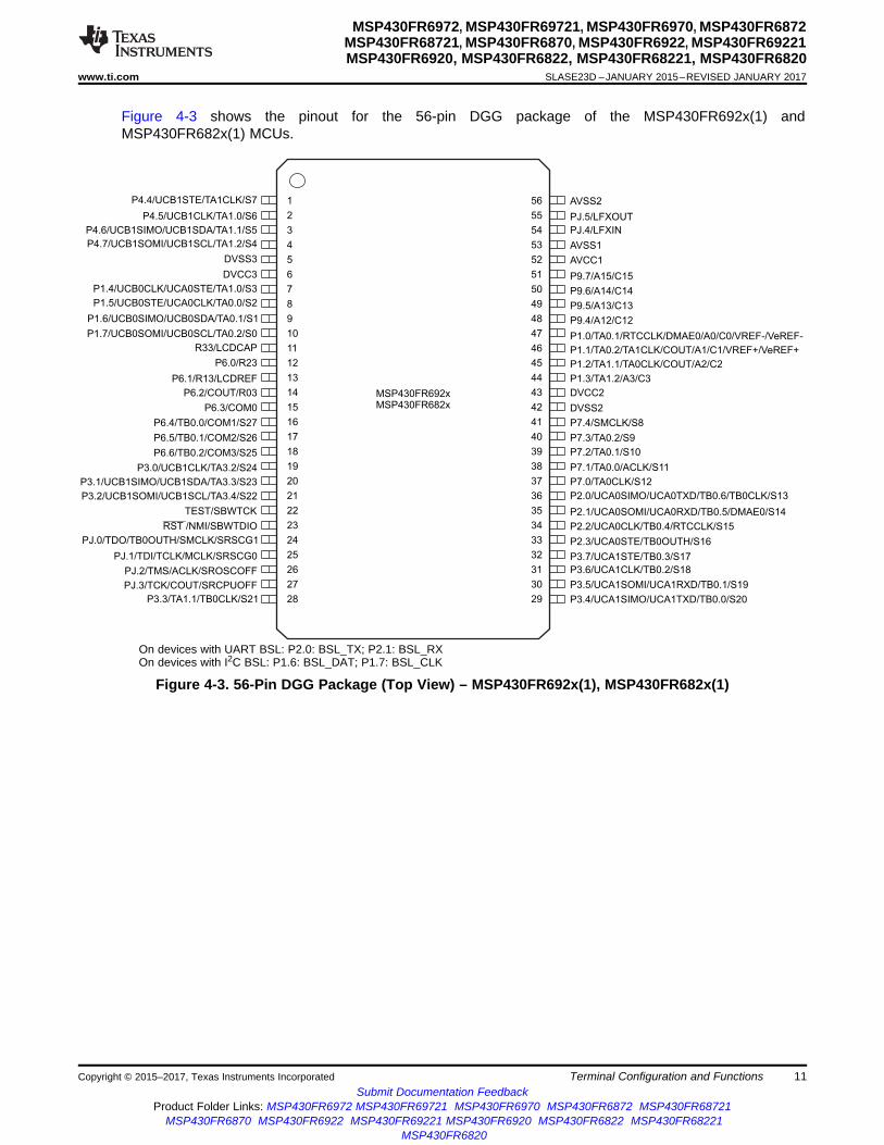
4.1 Pin DiagramsFigure 4-1 show the pinout for the 64-pin PM and RGC packages of the MSP430FR692x(1) andMSP430FR682x(1) MCUs.
On devices with UART BSL: P2.0: BSL_TX; P2.1: BSL_RXOn devices with I2C BSL: P1.6: BSL_DAT; P1.7: BSL_CLK
NOTE: TI recommends connecting the RGC package thermal pad to VSS.
Figure 4-1. 64-Pin PM and RGC Packages (Top View), MSP430FR692x(1) MSP430FR682x(1)

1P4.3/UCA0SOMI/UCA0RXD/UCB1STE/S4
2P1.4/UCB0CLK/UCA0STE/TA1.0/S3
3P1.5/UCB0STE/UCA0CLK/TA0.0/S2
4P1.6/ TA0.1/S1UCB0SIMO/UCB0SDA/
5P1.7/ TA0.2/S0UCB0SOMI/UCB0SCL/
6R33/LCDCAP
7P6.0/R23
8P6.1/R13/LCDREF
9P6.2/COUT/R03
10P6.3/COM0
11P6.4/TB0.0/COM1/S30
12P6.5/TB0.1/COM2/S29
13P6.6/TB0.2/COM3/S28
14P3.0/UCB1CLK/TA3.2/S27
15P3.1/ S26UCB1SIMO/UCB1SDA/TA3.3/
16P3.2/ S25UCB1SOMI/UCB1SCL/TA3.4/
17
DV
SS
1
18
DV
CC
1
19
TE
ST
/SB
WT
CK
20
RS
T/N
MI/S
BW
TD
IO
21
PJ.0
/TD
O/T
B0O
UT
H/S
MC
LK
/SR
SC
G1
22
PJ.1
/TD
I/T
CLK
/MC
LK
/SR
SC
G0
23
PJ.2
/TM
S/A
CLK
/SR
OS
CO
FF
24
PJ.3
/TC
K/C
OU
T/S
RC
PU
OF
F
25
P3.3
/TA
1.1
/TB
0C
LK
/S24
26
P3.4
/UC
A1S
IMO
/UC
A1T
XD
/TB
0.0
/S23
27
P3.5
/UC
A1S
OM
I/U
CA
1R
XD
/TB
0.1
/S22
28
P3.6
/UC
A1C
LK
/TB
0.2
/S21
29
P3.7
/UC
A1S
TE
/TB
0.3
/S20
30
P2.3
/UC
A0S
TE
/TB
0O
UT
H/S
19
31
P2.2
/UC
A0C
LK
/TB
0.4
/RT
CC
LK
/S18
32
P2.1
/UC
A0S
OM
I/U
CA
0R
XD
/TB
0.5
/DM
AE
0/S
17
33 P2.0/UCA0SIMO/UCA0TXD/TB0.6/TB0CLK/S16
34 P7.0/TA0CLK/S15
35 P7.1/TA0.0/ACLK/S14
36 P7.2/TA0.1/S13
37 P7.3/TA0.2/S12
38 P7.4/SMCLK/S11
39 DVSS2
40 DVCC2
41 P1.3/TA1.2/A3/C3
42 P1.2/TA1.1/TA0CLK/COUT/A2/C2
43 P1.1/TA0.2/TA1CLK/COUT/A1/C1/VREF+/VeREF+
44 P1.0/TA0.1/DMAE0/RTCCLK/A0/C0/VREF-/VeREF-
45 P9.4/A12/C12
46 P9.5/A13/C13
47 P9.6/A14/C14
48 P9.7/A15/C15
49
AV
CC
1
50
AV
SS
1
51
PJ.4
/LF
XIN
52
PJ.5
/LF
XO
UT
53
AV
SS
2
54555657
P5.7
/UC
A1S
TE
/TB
0C
LK
/S10
58
P4.4
/UC
B1S
TE
/TA
1C
LK
/S9
59
P4.5
/UC
B1C
LK
/TA
1.0
/S8
60P
4.6
/TA
1.1
/S7
UC
B1S
IMO
/UC
B1S
DA
/61
P4.7
/TA
1.2
/S6
UC
B1S
OM
I/U
CB
1S
CL/
62
DV
SS
3
63
DV
CC
3
64
P4.2
/UC
A0S
IMO
/UC
A0T
XD
/UC
B1C
LK
/S5
MSP430FR697x
MSP430FR687x
AV
SS
3
PJ.7
/HF
XO
UT
PJ.6
/HF
XIN
10
MSP430FR6972, MSP430FR69721, MSP430FR6970, MSP430FR6872MSP430FR68721, MSP430FR6870, MSP430FR6922, MSP430FR69221MSP430FR6920, MSP430FR6822, MSP430FR68221, MSP430FR6820SLASE23D –JANUARY 2015–REVISED JANUARY 2017 www.ti.com
Submit Documentation FeedbackProduct Folder Links: MSP430FR6972 MSP430FR69721 MSP430FR6970 MSP430FR6872 MSP430FR68721
MSP430FR6870 MSP430FR6922 MSP430FR69221 MSP430FR6920 MSP430FR6822 MSP430FR68221MSP430FR6820
Terminal Configuration and Functions Copyright © 2015–2017, Texas Instruments Incorporated
Figure 4-2 shows the pinout for the 64-pin PM and RGC packages of the MSP430FR697x(1) andMSP430FR687x(1) MCUs.
On devices with UART BSL: P2.0: BSL_TX; P2.1: BSL_RXOn devices with I2C BSL: P1.6: BSL_DAT; P1.7: BSL_CLK
NOTE: TI recommends connecting the RGC package thermal pad to VSS.
Figure 4-2. 64-Pin PM and RGC Packages (Top View) – MSP430FR697x(1), MSP430FR687x(1)
43
44
45
46
47
48
49
50
51
52
53
54
55
56
15
16
17
18
19
20
21
22
23
24
25
26
27
28
7
8
9
10
11
12
13
14
29
30
31
32
33
34
35
36
37
38
39
40
41
42
1
2
3
4
5
6
MSP430FR692x
MSP430FR682x
P1.4/UCB0CLK/UCA0STE/TA1.0/S3
P1.5/UCB0STE/UCA0CLK/TA0.0/S2
P1.6/UCB0SIMO/UCB0SDA/TA0.1/S1
P1.7/UCB0SOMI/UCB0SCL/TA0.2/S0
R33/LCDCAP
P6.0/R23
P6.1/R13/LCDREF
P6.2/COUT/R03
P6.3/COM0
P6.4/TB0.0/COM1/S27
P6.5/TB0.1/COM2/S26
P6.6/TB0.2/COM3/S25
P3.0/UCB1CLK/TA3.2/S24
P3.1/UCB1SIMO/UCB1SDA/TA3.3/S23
P3.2/UCB1SOMI/UCB1SCL/TA3.4/S22
DVSS2
DVCC2
TEST/SBWTCK
RST /NMI/SBWTDIO
PJ.0/TDO/TB0OUTH/SMCLK/SRSCG1
PJ.1/TDI/TCLK/MCLK/SRSCG0
PJ.2/TMS/ACLK/SROSCOFF
PJ.3/TCK/COUT/SRCPUOFF
P3.3/TA1.1/TB0CLK/S21 P3.4/UCA1SIMO/UCA1TXD/TB0.0/S20
P3.5/UCA1SOMI/UCA1RXD/TB0.1/S19
P3.6/UCA1CLK/TB0.2/S18
P3.7/UCA1STE/TB0.3/S17
P2.3/UCA0STE/TB0OUTH/S16
P2.2/UCA0CLK/TB0.4/RTCCLK/S15
P2.1/UCA0SOMI/UCA0RXD/TB0.5/DMAE0/S14
P2.0/UCA0SIMO/UCA0TXD/TB0.6/TB0CLK/S13
P7.0/TA0CLK/S12
P7.1/TA0.0/ACLK/S11
P7.2/TA0.1/S10
P7.3/TA0.2/S9
P7.4/SMCLK/S8
DVSS3
DVCC3
P1.3/TA1.2/A3/C3
P1.2/TA1.1/TA0CLK/COUT/A2/C2
P1.1/TA0.2/TA1CLK/COUT/A1/C1/VREF+/VeREF+
P1.0/TA0.1/RTCCLK/DMAE0/A0/C0/VREF-/VeREF-
AVCC1
AVSS1
PJ.4/LFXIN
PJ.5/LFXOUT
AVSS2P4.4/UCB1STE/TA1CLK/S7
P4.5/UCB1CLK/TA1.0/S6
P4.6/UCB1SIMO/UCB1SDA/TA1.1/S5
P4.7/UCB1SOMI/UCB1SCL/TA1.2/S4
P9.4/A12/C12
P9.5/A13/C13
P9.6/A14/C14
P9.7/A15/C15
11
MSP430FR6972, MSP430FR69721, MSP430FR6970, MSP430FR6872MSP430FR68721, MSP430FR6870, MSP430FR6922, MSP430FR69221MSP430FR6920, MSP430FR6822, MSP430FR68221, MSP430FR6820
www.ti.com SLASE23D –JANUARY 2015–REVISED JANUARY 2017
Submit Documentation FeedbackProduct Folder Links: MSP430FR6972 MSP430FR69721 MSP430FR6970 MSP430FR6872 MSP430FR68721
MSP430FR6870 MSP430FR6922 MSP430FR69221 MSP430FR6920 MSP430FR6822 MSP430FR68221MSP430FR6820
Terminal Configuration and FunctionsCopyright © 2015–2017, Texas Instruments Incorporated
Figure 4-3 shows the pinout for the 56-pin DGG package of the MSP430FR692x(1) andMSP430FR682x(1) MCUs.
On devices with UART BSL: P2.0: BSL_TX; P2.1: BSL_RXOn devices with I2C BSL: P1.6: BSL_DAT; P1.7: BSL_CLK
Figure 4-3. 56-Pin DGG Package (Top View) – MSP430FR692x(1), MSP430FR682x(1)

12
MSP430FR6972, MSP430FR69721, MSP430FR6970, MSP430FR6872MSP430FR68721, MSP430FR6870, MSP430FR6922, MSP430FR69221MSP430FR6920, MSP430FR6822, MSP430FR68221, MSP430FR6820SLASE23D –JANUARY 2015–REVISED JANUARY 2017 www.ti.com
Submit Documentation FeedbackProduct Folder Links: MSP430FR6972 MSP430FR69721 MSP430FR6970 MSP430FR6872 MSP430FR68721
MSP430FR6870 MSP430FR6922 MSP430FR69221 MSP430FR6920 MSP430FR6822 MSP430FR68221MSP430FR6820
Terminal Configuration and Functions Copyright © 2015–2017, Texas Instruments Incorporated
(1) Signals names with (RD) denote the reset default pin name.(2) To determine the pin mux encodings for each pin, see the Port I/O Diagrams section.(3) Sz = The LCD segment that is assigned to each pin can vary by package – see the "LCD SEG" columns for the assignment on this pin.(4) Signal Types: I = Input, O = Output, I/O = Input or Output.(5) Buffer Types: LVCMOS, Analog, or Power (see Table 4-3 for details)(6) Reset States:
OFF = High impedance with Schmitt-trigger inputs and pullup or pulldown (if available) disabledN/A = Not applicable
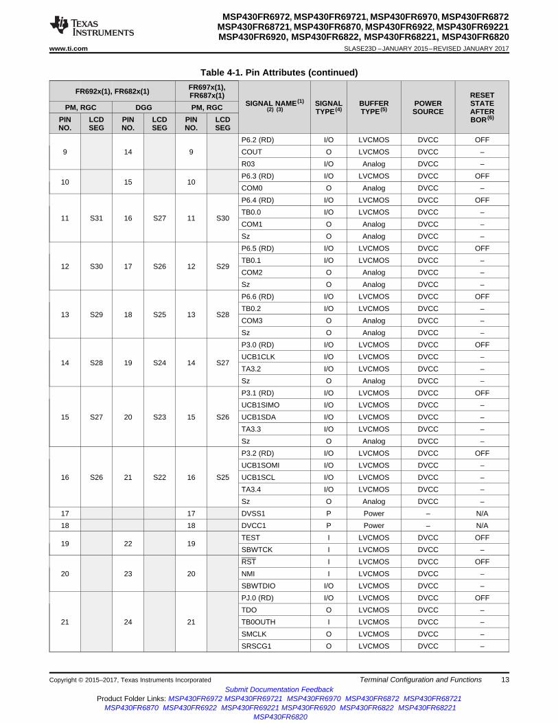
4.2 Pin AttributesTable 4-1 lists the attributes of each pin.
Table 4-1. Pin Attributes
FR692x(1), FR682x(1) FR697x(1),FR687x(1)
SIGNAL NAME (1)(2) (3)
SIGNALTYPE (4)
BUFFERTYPE (5)
POWERSOURCE
RESETSTATEAFTERBOR (6)
PM, RGC DGG PM, RGCPINNO.
LCDSEG
PINNO.
LCDSEG
PINNO.
LCDSEG
1 1 S4
P4.3 (RD) I/O LVCMOS DVCC OFFUCA0SOMI I/O LVCMOS DVCC –UCA0RXD I LVCMOS DVCC –UCB1STE I/O LVCMOS DVCC –Sz O Analog DVCC –
2 S3 7 S3 2 S3
P1.4 (RD) I/O LVCMOS DVCC OFFUCB0CLK I/O LVCMOS DVCC –UCA0STE I/O LVCMOS DVCC –TA1.0 I/O LVCMOS DVCC –Sz O Analog DVCC –
3 S2 8 S2 3 S2
P1.5 (RD) I/O LVCMOS DVCC OFFUCB0STE I/O LVCMOS DVCC –UCA0CLK I/O LVCMOS DVCC –TA0.0 I/O LVCMOS DVCC –Sz O Analog DVCC –
4 S1 9 S1 4 S1
P1.6 (RD) I/O LVCMOS DVCC OFFUCB0SIMO I/O LVCMOS DVCC –UCB0SDA I/O LVCMOS DVCC –BSL_DAT I LVCMOS DVCC –TA0.1 I/O LVCMOS DVCC –Sz O Analog DVCC –
5 S0 10 S0 5 S0
P1.7 (RD) I/O LVCMOS DVCC OFFUCB0SOMI I/O LVCMOS DVCC –UCB0SCL I/O LVCMOS DVCC –BSL_CLK I LVCMOS DVCC –TA0.2 I/O LVCMOS DVCC –Sz O Analog DVCC –
6 11 6R33 I/O Analog DVCC –LCDCAP I/O Analog DVCC –
7 12 7P6.0 (RD) I/O LVCMOS DVCC OFFR23 I/O Analog DVCC –
8 13 8P6.1 (RD) I/O LVCMOS DVCC OFFR13 I/O Analog DVCC –LCDREF I Analog – –
13
MSP430FR6972, MSP430FR69721, MSP430FR6970, MSP430FR6872MSP430FR68721, MSP430FR6870, MSP430FR6922, MSP430FR69221MSP430FR6920, MSP430FR6822, MSP430FR68221, MSP430FR6820
www.ti.com SLASE23D –JANUARY 2015–REVISED JANUARY 2017
Submit Documentation FeedbackProduct Folder Links: MSP430FR6972 MSP430FR69721 MSP430FR6970 MSP430FR6872 MSP430FR68721
MSP430FR6870 MSP430FR6922 MSP430FR69221 MSP430FR6920 MSP430FR6822 MSP430FR68221MSP430FR6820
Terminal Configuration and FunctionsCopyright © 2015–2017, Texas Instruments Incorporated
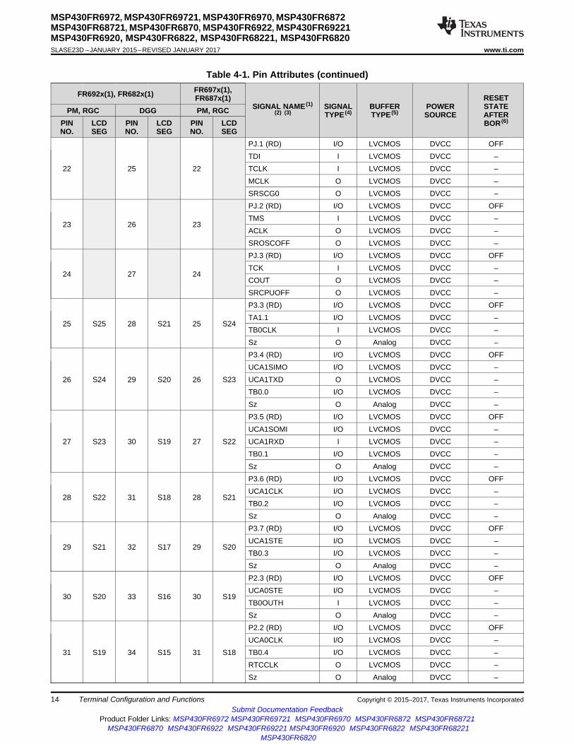
Table 4-1. Pin Attributes (continued)
FR692x(1), FR682x(1) FR697x(1),FR687x(1)
SIGNAL NAME (1)(2) (3)
SIGNALTYPE (4)
BUFFERTYPE (5)
POWERSOURCE
RESETSTATEAFTERBOR (6)
PM, RGC DGG PM, RGCPINNO.
LCDSEG
PINNO.
LCDSEG
PINNO.
LCDSEG
9 14 9P6.2 (RD) I/O LVCMOS DVCC OFFCOUT O LVCMOS DVCC –R03 I/O Analog DVCC –
10 15 10P6.3 (RD) I/O LVCMOS DVCC OFFCOM0 O Analog DVCC –
11 S31 16 S27 11 S30
P6.4 (RD) I/O LVCMOS DVCC OFFTB0.0 I/O LVCMOS DVCC –COM1 O Analog DVCC –Sz O Analog DVCC –
12 S30 17 S26 12 S29
P6.5 (RD) I/O LVCMOS DVCC OFFTB0.1 I/O LVCMOS DVCC –COM2 O Analog DVCC –Sz O Analog DVCC –
13 S29 18 S25 13 S28
P6.6 (RD) I/O LVCMOS DVCC OFFTB0.2 I/O LVCMOS DVCC –COM3 O Analog DVCC –Sz O Analog DVCC –
14 S28 19 S24 14 S27
P3.0 (RD) I/O LVCMOS DVCC OFFUCB1CLK I/O LVCMOS DVCC –TA3.2 I/O LVCMOS DVCC –Sz O Analog DVCC –
15 S27 20 S23 15 S26
P3.1 (RD) I/O LVCMOS DVCC OFFUCB1SIMO I/O LVCMOS DVCC –UCB1SDA I/O LVCMOS DVCC –TA3.3 I/O LVCMOS DVCC –Sz O Analog DVCC –
16 S26 21 S22 16 S25
P3.2 (RD) I/O LVCMOS DVCC OFFUCB1SOMI I/O LVCMOS DVCC –UCB1SCL I/O LVCMOS DVCC –TA3.4 I/O LVCMOS DVCC –Sz O Analog DVCC –
17 17 DVSS1 P Power – N/A18 18 DVCC1 P Power – N/A
19 22 19TEST I LVCMOS DVCC OFFSBWTCK I LVCMOS DVCC –
20 23 20RST I LVCMOS DVCC OFFNMI I LVCMOS DVCC –SBWTDIO I/O LVCMOS DVCC –
21 24 21
PJ.0 (RD) I/O LVCMOS DVCC OFFTDO O LVCMOS DVCC –TB0OUTH I LVCMOS DVCC –SMCLK O LVCMOS DVCC –SRSCG1 O LVCMOS DVCC –
14
MSP430FR6972, MSP430FR69721, MSP430FR6970, MSP430FR6872MSP430FR68721, MSP430FR6870, MSP430FR6922, MSP430FR69221MSP430FR6920, MSP430FR6822, MSP430FR68221, MSP430FR6820SLASE23D –JANUARY 2015–REVISED JANUARY 2017 www.ti.com
Submit Documentation FeedbackProduct Folder Links: MSP430FR6972 MSP430FR69721 MSP430FR6970 MSP430FR6872 MSP430FR68721
MSP430FR6870 MSP430FR6922 MSP430FR69221 MSP430FR6920 MSP430FR6822 MSP430FR68221MSP430FR6820
Terminal Configuration and Functions Copyright © 2015–2017, Texas Instruments Incorporated
Table 4-1. Pin Attributes (continued)
FR692x(1), FR682x(1) FR697x(1),FR687x(1)
SIGNAL NAME (1)(2) (3)
SIGNALTYPE (4)
BUFFERTYPE (5)
POWERSOURCE
RESETSTATEAFTERBOR (6)
PM, RGC DGG PM, RGCPINNO.
LCDSEG
PINNO.
LCDSEG
PINNO.
LCDSEG
22 25 22
PJ.1 (RD) I/O LVCMOS DVCC OFFTDI I LVCMOS DVCC –TCLK I LVCMOS DVCC –MCLK O LVCMOS DVCC –SRSCG0 O LVCMOS DVCC –
23 26 23
PJ.2 (RD) I/O LVCMOS DVCC OFFTMS I LVCMOS DVCC –ACLK O LVCMOS DVCC –SROSCOFF O LVCMOS DVCC –
24 27 24
PJ.3 (RD) I/O LVCMOS DVCC OFFTCK I LVCMOS DVCC –COUT O LVCMOS DVCC –SRCPUOFF O LVCMOS DVCC –
25 S25 28 S21 25 S24
P3.3 (RD) I/O LVCMOS DVCC OFFTA1.1 I/O LVCMOS DVCC –TB0CLK I LVCMOS DVCC –Sz O Analog DVCC –
26 S24 29 S20 26 S23
P3.4 (RD) I/O LVCMOS DVCC OFFUCA1SIMO I/O LVCMOS DVCC –UCA1TXD O LVCMOS DVCC –TB0.0 I/O LVCMOS DVCC –Sz O Analog DVCC –
27 S23 30 S19 27 S22
P3.5 (RD) I/O LVCMOS DVCC OFFUCA1SOMI I/O LVCMOS DVCC –UCA1RXD I LVCMOS DVCC –TB0.1 I/O LVCMOS DVCC –Sz O Analog DVCC –
28 S22 31 S18 28 S21
P3.6 (RD) I/O LVCMOS DVCC OFFUCA1CLK I/O LVCMOS DVCC –TB0.2 I/O LVCMOS DVCC –Sz O Analog DVCC –
29 S21 32 S17 29 S20
P3.7 (RD) I/O LVCMOS DVCC OFFUCA1STE I/O LVCMOS DVCC –TB0.3 I/O LVCMOS DVCC –Sz O Analog DVCC –
30 S20 33 S16 30 S19
P2.3 (RD) I/O LVCMOS DVCC OFFUCA0STE I/O LVCMOS DVCC –TB0OUTH I LVCMOS DVCC –Sz O Analog DVCC –
31 S19 34 S15 31 S18
P2.2 (RD) I/O LVCMOS DVCC OFFUCA0CLK I/O LVCMOS DVCC –TB0.4 I/O LVCMOS DVCC –RTCCLK O LVCMOS DVCC –Sz O Analog DVCC –

15
MSP430FR6972, MSP430FR69721, MSP430FR6970, MSP430FR6872MSP430FR68721, MSP430FR6870, MSP430FR6922, MSP430FR69221MSP430FR6920, MSP430FR6822, MSP430FR68221, MSP430FR6820
www.ti.com SLASE23D –JANUARY 2015–REVISED JANUARY 2017
Submit Documentation FeedbackProduct Folder Links: MSP430FR6972 MSP430FR69721 MSP430FR6970 MSP430FR6872 MSP430FR68721
MSP430FR6870 MSP430FR6922 MSP430FR69221 MSP430FR6920 MSP430FR6822 MSP430FR68221MSP430FR6820
Terminal Configuration and FunctionsCopyright © 2015–2017, Texas Instruments Incorporated
Table 4-1. Pin Attributes (continued)
FR692x(1), FR682x(1) FR697x(1),FR687x(1)
SIGNAL NAME (1)(2) (3)
SIGNALTYPE (4)
BUFFERTYPE (5)
POWERSOURCE
RESETSTATEAFTERBOR (6)
PM, RGC DGG PM, RGCPINNO.
LCDSEG
PINNO.
LCDSEG
PINNO.
LCDSEG
32 S18 35 S14 32 S17
P2.1 (RD) I/O LVCMOS DVCC OFFUCA0SOMI I/O LVCMOS DVCC –UCA0RXD I LVCMOS DVCC –BSL_RX I LVCMOS DVCC –TB0.5 I/O LVCMOS DVCC –DMAE0 I LVCMOS DVCC –Sz O Analog DVCC –
33 S17 36 S13 33 S16
P2.0 (RD) I/O LVCMOS DVCC OFFUCA0SIMO I/O LVCMOS DVCC –UCA0TXD O LVCMOS DVCC –BSL_TX O LVCMOS DVCC –TB0.6 I/O LVCMOS DVCC –TB0CLK I LVCMOS DVCC –Sz O Analog DVCC –
34 S16 37 S12 34 S15P7.0 (RD) I/O LVCMOS DVCC OFFTA0CLK I LVCMOS DVCC –Sz O Analog DVCC –
35 S15 38 S11 35 S14
P7.1 (RD) I/O LVCMOS DVCC OFFTA0.0 I/O LVCMOS DVCC –ACLK O LVCMOS DVCC –Sz O Analog DVCC –
36 S14 39 S10 36 S13P7.2 (RD) I/O LVCMOS DVCC OFFTA0.1 I/O LVCMOS DVCC –Sz O Analog DVCC –
37 S13 40 S9 37 S12P7.3 (RD) I/O LVCMOS DVCC OFFTA0.2 I/O LVCMOS DVCC –Sz O Analog DVCC –
38 S12 41 S8 38 S11P7.4 (RD) I/O LVCMOS DVCC OFFSMCLK O LVCMOS DVCC –Sz O Analog DVCC –
39 42 39 DVSS2 P Power – N/A40 43 40 DVCC2 P Power – N/A
41 44 41
P1.3 (RD) I/O LVCMOS DVCC OFFTA1.2 I/O LVCMOS DVCC –A3 I Analog AVCC –C3 I Analog AVCC –
42 45 42
P1.2 (RD) I/O LVCMOS DVCC OFFTA1.1 I/O LVCMOS DVCC –TA0CLK I LVCMOS DVCC –COUT O LVCMOS DVCC –A2 I Analog AVCC –C2 I Analog AVCC –

16
MSP430FR6972, MSP430FR69721, MSP430FR6970, MSP430FR6872MSP430FR68721, MSP430FR6870, MSP430FR6922, MSP430FR69221MSP430FR6920, MSP430FR6822, MSP430FR68221, MSP430FR6820SLASE23D –JANUARY 2015–REVISED JANUARY 2017 www.ti.com
Submit Documentation FeedbackProduct Folder Links: MSP430FR6972 MSP430FR69721 MSP430FR6970 MSP430FR6872 MSP430FR68721
MSP430FR6870 MSP430FR6922 MSP430FR69221 MSP430FR6920 MSP430FR6822 MSP430FR68221MSP430FR6820
Terminal Configuration and Functions Copyright © 2015–2017, Texas Instruments Incorporated
Table 4-1. Pin Attributes (continued)
FR692x(1), FR682x(1) FR697x(1),FR687x(1)
SIGNAL NAME (1)(2) (3)
SIGNALTYPE (4)
BUFFERTYPE (5)
POWERSOURCE
RESETSTATEAFTERBOR (6)
PM, RGC DGG PM, RGCPINNO.
LCDSEG
PINNO.
LCDSEG
PINNO.
LCDSEG
43 46 43
P1.1 (RD) I/O LVCMOS DVCC OFFTA0.2 I/O LVCMOS DVCC –TA1CLK I LVCMOS DVCC –COUT O LVCMOS DVCC –A1 I Analog AVCC –C1 I Analog AVCC –VREF+ O Analog AVCC –VeREF+ I Analog – –
44 47 44
P1.0 (RD) I/O LVCMOS DVCC OFFTA0.1 I/O LVCMOS DVCC –DMAE0 I LVCMOS DVCC –RTCCLK O LVCMOS DVCC –A0 I Analog AVCC –C0 I Analog AVCC –VREF- O Analog AVCC –VeREF- I Analog – –
45 48 45P9.4 (RD) I/O LVCMOS DVCC OFFA12 I Analog AVCC –C12 I Analog AVCC –
46 49 46P9.5 (RD) I/O LVCMOS DVCC OFFA13 I Analog AVCC –C13 I Analog AVCC –
47 50 47P9.6 (RD) I/O LVCMOS DVCC OFFA14 I Analog AVCC –C14 I Analog AVCC –
48 51 48P9.7 (RD) I/O LVCMOS DVCC OFFA15 I Analog AVCC –C15 I Analog AVCC –
49 52 49 AVCC1 P Power – N/A50 53 50 AVSS1 P Power – N/A
51 54 51PJ.4 (RD) I/O LVCMOS DVCC OFFLFXIN I Analog AVCC –
52 55 52PJ.5 (RD) I/O LVCMOS DVCC OFFLFXOUT O Analog AVCC –
53 56 53 AVSS2 P Power – N/A
54PJ.7 (RD) I/O LVCMOS DVCC OFFHFXOUT O Analog AVCC –
55PJ.6 (RD) I/O LVCMOS DVCC OFFHFXIN I Analog AVCC –
56 AVSS3 P Power – N/A
54 S11
P5.4 (RD) I/O LVCMOS DVCC OFFUCA1SIMO I/O LVCMOS DVCC –UCA1TXD O LVCMOS DVCC –Sz O Analog DVCC –

17
MSP430FR6972, MSP430FR69721, MSP430FR6970, MSP430FR6872MSP430FR68721, MSP430FR6870, MSP430FR6922, MSP430FR69221MSP430FR6920, MSP430FR6822, MSP430FR68221, MSP430FR6820
www.ti.com SLASE23D –JANUARY 2015–REVISED JANUARY 2017
Submit Documentation FeedbackProduct Folder Links: MSP430FR6972 MSP430FR69721 MSP430FR6970 MSP430FR6872 MSP430FR68721
MSP430FR6870 MSP430FR6922 MSP430FR69221 MSP430FR6920 MSP430FR6822 MSP430FR68221MSP430FR6820
Terminal Configuration and FunctionsCopyright © 2015–2017, Texas Instruments Incorporated
Table 4-1. Pin Attributes (continued)
FR692x(1), FR682x(1) FR697x(1),FR687x(1)
SIGNAL NAME (1)(2) (3)
SIGNALTYPE (4)
BUFFERTYPE (5)
POWERSOURCE
RESETSTATEAFTERBOR (6)
PM, RGC DGG PM, RGCPINNO.
LCDSEG
PINNO.
LCDSEG
PINNO.
LCDSEG
55 S10
P5.5 (RD) I/O LVCMOS DVCC OFFUCA1SOMI I/O LVCMOS DVCC –UCA1RXD I LVCMOS DVCC –Sz O Analog DVCC –
56 S9P5.6 (RD) I/O LVCMOS DVCC OFFUCA1CLK I/O LVCMOS DVCC –Sz O Analog DVCC –
57 S8 57 S10
P5.7 (RD) I/O LVCMOS DVCC OFFUCA1STE I/O LVCMOS DVCC –TB0CLK I LVCMOS DVCC –Sz O Analog DVCC –
58 S7 1 S7 58 S9
P4.4 (RD) I/O LVCMOS DVCC OFFUCB1STE I/O LVCMOS DVCC –TA1CLK I LVCMOS DVCC –Sz O Analog DVCC –
59 S6 2 S6 59 S8
P4.5 (RD) I/O LVCMOS DVCC OFFUCB1CLK I/O LVCMOS DVCC –TA1.0 I/O LVCMOS DVCC –Sz O Analog DVCC –
60 S5 3 S5 60 S7
P4.6 (RD) I/O LVCMOS DVCC OFFUCB1SIMO I/O LVCMOS DVCC –UCB1SDA I/O LVCMOS DVCC –TA1.1 I/O LVCMOS DVCC –Sz O Analog DVCC –
61 S4 4 S4 61 S6
P4.7 (RD) I/O LVCMOS DVCC OFFUCB1SOMI I/O LVCMOS DVCC –UCB1SCL I/O LVCMOS DVCC –TA1.2 I/O LVCMOS DVCC –Sz O Analog DVCC –
62 5 62 DVSS3 P Power – N/A63 6 63 DVCC3 P Power – N/A
64 64 S5
P4.2 (RD) I/O LVCMOS DVCC OFFUCA0SIMO I/O LVCMOS DVCC –UCA0TXD O LVCMOS DVCC –UCB1CLK I/O LVCMOS DVCC –Sz O Analog DVCC –

18
MSP430FR6972, MSP430FR69721, MSP430FR6970, MSP430FR6872MSP430FR68721, MSP430FR6870, MSP430FR6922, MSP430FR69221MSP430FR6920, MSP430FR6822, MSP430FR68221, MSP430FR6820SLASE23D –JANUARY 2015–REVISED JANUARY 2017 www.ti.com
Submit Documentation FeedbackProduct Folder Links: MSP430FR6972 MSP430FR69721 MSP430FR6970 MSP430FR6872 MSP430FR68721
MSP430FR6870 MSP430FR6922 MSP430FR69221 MSP430FR6920 MSP430FR6822 MSP430FR68221MSP430FR6820
Terminal Configuration and Functions Copyright © 2015–2017, Texas Instruments Incorporated
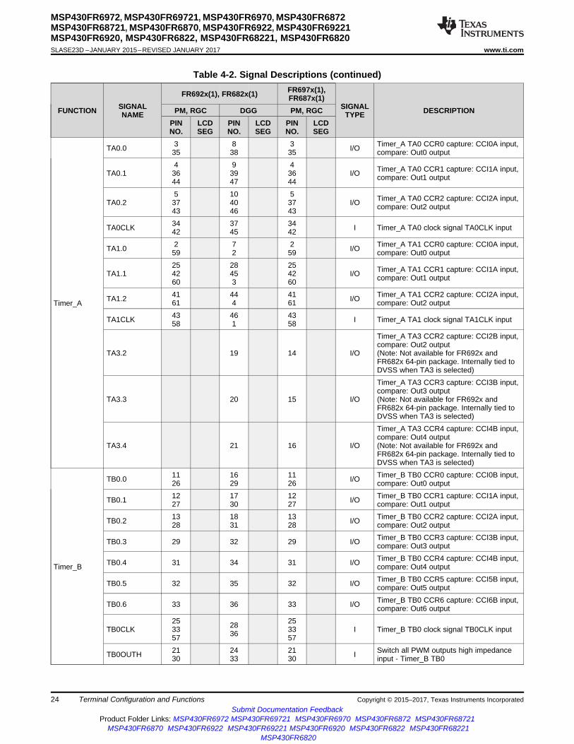
4.3 Signal DescriptionsTable 4-2 describes the signals.
Table 4-2. Signal Descriptions
FUNCTION SIGNALNAME
FR692x(1), FR682x(1) FR697x(1),FR687x(1)
SIGNALTYPE DESCRIPTIONPM, RGC DGG PM, RGC
PINNO.
LCDSEG
PINNO.
LCDSEG
PINNO.
LCDSEG
ADC
A0 44 47 44 I Analog input A0A1 43 46 43 I Analog input A1A2 42 45 42 I Analog input A2A3 41 44 41 I Analog input A3A12 45 48 45 I Analog input A12A13 46 49 46 I Analog input A13A14 47 50 47 I Analog input A14A15 48 51 48 I Analog input A15VREF+ 43 46 43 O Output of positive reference voltageVREF- 44 47 44 O Output of negative reference voltage
VeREF+ 43 46 43 I Input for an external positive referencevoltage to the ADC
VeREF- 44 47 44 I Input for an external negative referencevoltage to the ADC
BSL (I2C)BSL_CLK 5 10 5 I BSL clock (I2C BSL)BSL_DAT 4 9 4 I/O BSL data (I2C BSL)
BSL (UART)BSL_RX 32 35 32 I BSL receive (UART BSL)BSL_TX 33 36 33 O BSL transmit (UART BSL)
Clock
ACLK 2335
2638
2335 O ACLK output
HFXIN 55 I Input terminal of crystal oscillator XT2HFXOUT 54 O Output terminal for crystal oscillator XT2LFXIN 51 54 51 I Input terminal for crystal oscillator XT1LFXOUT 52 55 52 O Output terminal of crystal oscillator XT1MCLK 22 25 22 O MCLK output
RTCCLK 3144
3447
3144 O RTC clock output for calibration
SMCLK 2138
2441
2138 O SMCLK output
Comparator
C0 44 47 44 I Comparator input C0C1 43 46 43 I Comparator input C1C2 42 45 42 I Comparator input C2C3 41 44 41 I Comparator input C3C12 45 48 45 I Comparator input C12C13 46 49 46 I Comparator input C13C14 47 50 47 I Comparator input C14C15 48 51 48 I Comparator input C15
COUT
9244243
14274546
9244243
O Comparator output

19
MSP430FR6972, MSP430FR69721, MSP430FR6970, MSP430FR6872MSP430FR68721, MSP430FR6870, MSP430FR6922, MSP430FR69221MSP430FR6920, MSP430FR6822, MSP430FR68221, MSP430FR6820
www.ti.com SLASE23D –JANUARY 2015–REVISED JANUARY 2017
Submit Documentation FeedbackProduct Folder Links: MSP430FR6972 MSP430FR69721 MSP430FR6970 MSP430FR6872 MSP430FR68721
MSP430FR6870 MSP430FR6922 MSP430FR69221 MSP430FR6920 MSP430FR6822 MSP430FR68221MSP430FR6820
Terminal Configuration and FunctionsCopyright © 2015–2017, Texas Instruments Incorporated
Table 4-2. Signal Descriptions (continued)
FUNCTION SIGNALNAME
FR692x(1), FR682x(1) FR697x(1),FR687x(1)
SIGNALTYPE DESCRIPTIONPM, RGC DGG PM, RGC
PINNO.
LCDSEG
PINNO.
LCDSEG
PINNO.
LCDSEG
Debug
SBWTCK 19 22 19 I Spy-Bi-Wire input clockSBWTDIO 20 23 20 I/O Spy-Bi-Wire data input/output
SRCPUOFF 24 27 24 O Low-power debug: CPU status registerCPUOFF
SROSCOFF 23 26 23 O Low-power debug: CPU status registerOSCOFF
SRSCG0 22 25 22 O Low-power debug: CPU status registerSCG0
SRSCG1 21 24 21 O Low-power debug: CPU status registerSCG1
TCK 24 27 24 I Test clockTCLK 22 25 22 I Test clock inputTDI 22 25 22 I Test data inputTDO 21 24 21 O Test data output port
TEST 19 22 19 I Test mode pin - select digital I/O on JTAGpins
TMS 23 26 23 I Test mode select
DMA DMAE0 3244
3547
3244 I DMA external trigger input
GPIO
P1.0 44 47 44 I/O General-purpose digital I/OP1.1 43 46 43 I/O General-purpose digital I/OP1.2 42 45 42 I/O General-purpose digital I/OP1.3 41 44 41 I/O General-purpose digital I/OP1.4 2 7 2 I/O General-purpose digital I/OP1.5 3 8 3 I/O General-purpose digital I/OP1.6 4 9 4 I/O General-purpose digital I/OP1.7 5 10 5 I/O General-purpose digital I/OP2.0 33 36 33 I/O General-purpose digital I/OP2.1 32 35 32 I/O General-purpose digital I/OP2.2 31 34 31 I/O General-purpose digital I/OP2.3 30 33 30 I/O General-purpose digital I/OP3.0 14 19 14 I/O General-purpose digital I/OP3.1 15 20 15 I/O General-purpose digital I/OP3.2 16 21 16 I/O General-purpose digital I/OP3.3 25 28 25 I/O General-purpose digital I/OP3.4 26 29 26 I/O General-purpose digital I/OP3.5 27 30 27 I/O General-purpose digital I/OP3.6 28 31 28 I/O General-purpose digital I/OP3.7 29 32 29 I/O General-purpose digital I/O

20
MSP430FR6972, MSP430FR69721, MSP430FR6970, MSP430FR6872MSP430FR68721, MSP430FR6870, MSP430FR6922, MSP430FR69221MSP430FR6920, MSP430FR6822, MSP430FR68221, MSP430FR6820SLASE23D –JANUARY 2015–REVISED JANUARY 2017 www.ti.com
Submit Documentation FeedbackProduct Folder Links: MSP430FR6972 MSP430FR69721 MSP430FR6970 MSP430FR6872 MSP430FR68721
MSP430FR6870 MSP430FR6922 MSP430FR69221 MSP430FR6920 MSP430FR6822 MSP430FR68221MSP430FR6820
Terminal Configuration and Functions Copyright © 2015–2017, Texas Instruments Incorporated
Table 4-2. Signal Descriptions (continued)
FUNCTION SIGNALNAME
FR692x(1), FR682x(1) FR697x(1),FR687x(1)
SIGNALTYPE DESCRIPTIONPM, RGC DGG PM, RGC
PINNO.
LCDSEG
PINNO.
LCDSEG
PINNO.
LCDSEG
GPIO
P4.2 64 64 I/O General-purpose digital I/OP4.3 1 1 I/O General-purpose digital I/OP4.4 58 1 58 I/O General-purpose digital I/OP4.5 59 2 59 I/O General-purpose digital I/OP4.6 60 3 60 I/O General-purpose digital I/OP4.7 61 4 61 I/O General-purpose digital I/OP5.4 54 I/O General-purpose digital I/OP5.5 55 I/O General-purpose digital I/OP5.6 56 I/O General-purpose digital I/OP5.7 57 57 I/O General-purpose digital I/OP6.0 7 12 7 I/O General-purpose digital I/OP6.1 8 13 8 I/O General-purpose digital I/OP6.2 9 14 9 I/O General-purpose digital I/OP6.3 10 15 10 I/O General-purpose digital I/OP6.4 11 16 11 I/O General-purpose digital I/OP6.5 12 17 12 I/O General-purpose digital I/OP6.6 13 18 13 I/O General-purpose digital I/OP7.0 34 37 34 I/O General-purpose digital I/OP7.1 35 38 35 I/O General-purpose digital I/OP7.2 36 39 36 I/O General-purpose digital I/OP7.3 37 40 37 I/O General-purpose digital I/OP7.4 38 41 38 I/O General-purpose digital I/OP9.4 45 48 45 I/O General-purpose digital I/OP9.5 46 49 46 I/O General-purpose digital I/OP9.6 47 50 47 I/O General-purpose digital I/OP9.7 48 51 48 I/O General-purpose digital I/OPJ.0 21 24 21 I/O General-purpose digital I/OPJ.1 22 25 22 I/O General-purpose digital I/OPJ.2 23 26 23 I/O General-purpose digital I/OPJ.3 24 27 24 I/O General-purpose digital I/OPJ.4 51 54 51 I/O General-purpose digital I/OPJ.5 52 55 52 I/O General-purpose digital I/OPJ.6 55 I/O General-purpose digital I/OPJ.7 54 I/O General-purpose digital I/O
I2C
UCB0SCL 5 10 5 I/O USCI_B0: I2C clock (I2C mode)UCB0SDA 4 9 4 I/O USCI_B0: I2C data (I2C mode)
UCB1SCL 1661
214
1661 I/O USCI_B1: I2C clock (I2C mode)
UCB1SDA 1560
203
1560 I/O USCI_B1: I2C data (I2C mode)

21
MSP430FR6972, MSP430FR69721, MSP430FR6970, MSP430FR6872MSP430FR68721, MSP430FR6870, MSP430FR6922, MSP430FR69221MSP430FR6920, MSP430FR6822, MSP430FR68221, MSP430FR6820
www.ti.com SLASE23D –JANUARY 2015–REVISED JANUARY 2017
Submit Documentation FeedbackProduct Folder Links: MSP430FR6972 MSP430FR69721 MSP430FR6970 MSP430FR6872 MSP430FR68721
MSP430FR6870 MSP430FR6922 MSP430FR69221 MSP430FR6920 MSP430FR6822 MSP430FR68221MSP430FR6820
Terminal Configuration and FunctionsCopyright © 2015–2017, Texas Instruments Incorporated
Table 4-2. Signal Descriptions (continued)
FUNCTION SIGNALNAME
FR692x(1), FR682x(1) FR697x(1),FR687x(1)
SIGNALTYPE DESCRIPTIONPM, RGC DGG PM, RGC
PINNO.
LCDSEG
PINNO.
LCDSEG
PINNO.
LCDSEG
LCD
COM0 10 15 10 O LCD common output COM0 for LCDbackplane
COM1 11 16 11 O LCD common output COM1 for LCDbackplane
COM2 12 17 12 O LCD common output COM2 for LCDbackplane
COM3 13 18 13 O LCD common output COM3 for LCDbackplane
LCDCAP 6 11 6 I LCD capacitor connection
LCDREF 8 13 8 I External reference voltage input forregulated LCD voltage
R03 9 14 9 I/O Input/output port of lowest analog LCDvoltage (V5)
R13 8 13 8 I/O Input/output port of third most positiveanalog LCD voltage (V3 or V4)
R23 7 12 7 I/O Input/output port of second most positiveanalog LCD voltage (V2)
R33 6 11 6 I/O Input/output port of most positive analogLCD voltage (V1)

22
MSP430FR6972, MSP430FR69721, MSP430FR6970, MSP430FR6872MSP430FR68721, MSP430FR6870, MSP430FR6922, MSP430FR69221MSP430FR6920, MSP430FR6822, MSP430FR68221, MSP430FR6820SLASE23D –JANUARY 2015–REVISED JANUARY 2017 www.ti.com
Submit Documentation FeedbackProduct Folder Links: MSP430FR6972 MSP430FR69721 MSP430FR6970 MSP430FR6872 MSP430FR68721
MSP430FR6870 MSP430FR6922 MSP430FR69221 MSP430FR6920 MSP430FR6822 MSP430FR68221MSP430FR6820
Terminal Configuration and Functions Copyright © 2015–2017, Texas Instruments Incorporated
Table 4-2. Signal Descriptions (continued)
FUNCTION SIGNALNAME
FR692x(1), FR682x(1) FR697x(1),FR687x(1)
SIGNALTYPE DESCRIPTIONPM, RGC DGG PM, RGC
PINNO.
LCDSEG
PINNO.
LCDSEG
PINNO.
LCDSEG
LCD Sz
1 S4 O
LCD segment output (package specific)
64 S5 O5 S0 10 S0 5 S0 O4 S1 9 S1 4 S1 O3 S2 8 S2 3 S2 O2 S3 7 S3 2 S3 O
61 S4 4 S4 61 S6 O60 S5 3 S5 60 S7 O59 S6 2 S6 59 S8 O58 S7 1 S7 58 S9 O57 S8 57 S10 O56 S9 O55 S10 O54 S11 O38 S12 41 S8 38 S11 O37 S13 40 S9 37 S12 O36 S14 39 S10 36 S13 O35 S15 38 S11 35 S14 O34 S16 37 S12 34 S15 O33 S17 36 S13 33 S16 O32 S18 35 S14 32 S17 O31 S19 34 S15 31 S18 O30 S20 33 S16 30 S19 O29 S21 32 S17 29 S20 O28 S22 31 S18 28 S21 O27 S23 30 S19 27 S22 O26 S24 29 S20 26 S23 O25 S25 28 S21 25 S24 O16 S26 21 S22 16 S25 O15 S27 20 S23 15 S26 O14 S28 19 S24 14 S27 O13 S29 18 S25 13 S28 O12 S30 17 S26 12 S29 O11 S31 16 S27 11 S30 O
Power
AVCC1 49 52 49 P Analog power supplyAVSS1 50 53 50 P Analog ground supplyAVSS2 53 56 53 P Analog ground supplyAVSS3 56 P Analog ground supplyDVCC1 18 18 P Digital power supplyDVCC2 40 43 40 P Digital power supplyDVCC3 63 6 63 P Digital power supplyDVSS1 17 17 P Digital ground supplyDVSS2 39 42 39 P Digital ground supplyDVSS3 62 5 62 P Digital ground supply

23
MSP430FR6972, MSP430FR69721, MSP430FR6970, MSP430FR6872MSP430FR68721, MSP430FR6870, MSP430FR6922, MSP430FR69221MSP430FR6920, MSP430FR6822, MSP430FR68221, MSP430FR6820
www.ti.com SLASE23D –JANUARY 2015–REVISED JANUARY 2017
Submit Documentation FeedbackProduct Folder Links: MSP430FR6972 MSP430FR69721 MSP430FR6970 MSP430FR6872 MSP430FR68721
MSP430FR6870 MSP430FR6922 MSP430FR69221 MSP430FR6920 MSP430FR6822 MSP430FR68221MSP430FR6820
Terminal Configuration and FunctionsCopyright © 2015–2017, Texas Instruments Incorporated
Table 4-2. Signal Descriptions (continued)
FUNCTION SIGNALNAME
FR692x(1), FR682x(1) FR697x(1),FR687x(1)
SIGNALTYPE DESCRIPTIONPM, RGC DGG PM, RGC
PINNO.
LCDSEG
PINNO.
LCDSEG
PINNO.
LCDSEG
SPI
UCA0CLK 331
834
331 I/O
USCI_A0: Clock signal input (SPI slavemode), Clock signal output (SPI mastermode)
UCA0SIMO 3364 36 33
64 I/O USCI_A0: Slave in, master out (SPI mode)
UCA0SOMI 132 35 1
32 I/O USCI_A0: Slave out, master in (SPI mode)
UCA0STE 230
733
230 I/O USCI_A0: Slave transmit enable (SPI
mode)
UCA1CLK 2856 31 28 I/O
USCI_A1: Clock signal input (SPI slavemode), Clock signal output (SPI mastermode)
UCA1SIMO 2654 29 26 I/O USCI_A1: Slave in, master out (SPI mode)
UCA1SOMI 2755 30 27 I/O USCI_A1: Slave out, master in (SPI mode)
UCA1STE 2957 32 29
57 I/O USCI_A1: Slave transmit enable (SPImode)
UCB0CLK 2 7 2 I/OUSCI_B0: Clock signal input (SPI slavemode), Clock signal output (SPI mastermode)
UCB0SIMO 4 9 4 I/O USCI_B0: Slave in, master out (SPI mode)UCB0SOMI 5 10 5 I/O USCI_B0: Slave out, master in (SPI mode)
UCB0STE 3 8 3 I/O USCI_B0: Slave transmit enable (SPImode)
UCB1CLK145964
192
145964
I/OUSCI_B1: Clock signal input (SPI slavemode), Clock signal output (SPI mastermode)
UCB1SIMO 6015
320
6015 I/O USCI_B1: Slave in, master out (SPI mode)
UCB1SOMI 1661
214
1661 I/O USCI_B1: Slave out, master in (SPI mode)
UCB1STE 158 1 1
58 I/O USCI_B1: Slave transmit enable (SPImode)
SystemNMI 20 23 20 I Nonmaskable interrupt inputRST 20 23 20 I Reset input active low
24
MSP430FR6972, MSP430FR69721, MSP430FR6970, MSP430FR6872MSP430FR68721, MSP430FR6870, MSP430FR6922, MSP430FR69221MSP430FR6920, MSP430FR6822, MSP430FR68221, MSP430FR6820SLASE23D –JANUARY 2015–REVISED JANUARY 2017 www.ti.com
Submit Documentation FeedbackProduct Folder Links: MSP430FR6972 MSP430FR69721 MSP430FR6970 MSP430FR6872 MSP430FR68721
MSP430FR6870 MSP430FR6922 MSP430FR69221 MSP430FR6920 MSP430FR6822 MSP430FR68221MSP430FR6820
Terminal Configuration and Functions Copyright © 2015–2017, Texas Instruments Incorporated
Table 4-2. Signal Descriptions (continued)
FUNCTION SIGNALNAME
FR692x(1), FR682x(1) FR697x(1),FR687x(1)
SIGNALTYPE DESCRIPTIONPM, RGC DGG PM, RGC
PINNO.
LCDSEG
PINNO.
LCDSEG
PINNO.
LCDSEG
Timer_A
TA0.0 335
838
335 I/O Timer_A TA0 CCR0 capture: CCI0A input,
compare: Out0 output
TA0.14
3644
93947
43644
I/O Timer_A TA0 CCR1 capture: CCI1A input,compare: Out1 output
TA0.25
3743
104046
53743
I/O Timer_A TA0 CCR2 capture: CCI2A input,compare: Out2 output
TA0CLK 3442
3745
3442 I Timer_A TA0 clock signal TA0CLK input
TA1.0 259
72
259 I/O Timer_A TA1 CCR0 capture: CCI0A input,
compare: Out0 output
TA1.1254260
28453
254260
I/O Timer_A TA1 CCR1 capture: CCI1A input,compare: Out1 output
TA1.2 4161
444
4161 I/O Timer_A TA1 CCR2 capture: CCI2A input,
compare: Out2 output
TA1CLK 4358
461
4358 I Timer_A TA1 clock signal TA1CLK input
TA3.2 19 14 I/O
Timer_A TA3 CCR2 capture: CCI2B input,compare: Out2 output(Note: Not available for FR692x andFR682x 64-pin package. Internally tied toDVSS when TA3 is selected)
TA3.3 20 15 I/O
Timer_A TA3 CCR3 capture: CCI3B input,compare: Out3 output(Note: Not available for FR692x andFR682x 64-pin package. Internally tied toDVSS when TA3 is selected)
TA3.4 21 16 I/O
Timer_A TA3 CCR4 capture: CCI4B input,compare: Out4 output(Note: Not available for FR692x andFR682x 64-pin package. Internally tied toDVSS when TA3 is selected)
Timer_B
TB0.0 1126
1629
1126 I/O Timer_B TB0 CCR0 capture: CCI0B input,
compare: Out0 output
TB0.1 1227
1730
1227 I/O Timer_B TB0 CCR1 capture: CCI1A input,
compare: Out1 output
TB0.2 1328
1831
1328 I/O Timer_B TB0 CCR2 capture: CCI2A input,
compare: Out2 output
TB0.3 29 32 29 I/O Timer_B TB0 CCR3 capture: CCI3B input,compare: Out3 output
TB0.4 31 34 31 I/O Timer_B TB0 CCR4 capture: CCI4B input,compare: Out4 output
TB0.5 32 35 32 I/O Timer_B TB0 CCR5 capture: CCI5B input,compare: Out5 output
TB0.6 33 36 33 I/O Timer_B TB0 CCR6 capture: CCI6B input,compare: Out6 output
TB0CLK253357
2836
253357
I Timer_B TB0 clock signal TB0CLK input
TB0OUTH 2130
2433
2130 I Switch all PWM outputs high impedance
input - Timer_B TB0

25
MSP430FR6972, MSP430FR69721, MSP430FR6970, MSP430FR6872MSP430FR68721, MSP430FR6870, MSP430FR6922, MSP430FR69221MSP430FR6920, MSP430FR6822, MSP430FR68221, MSP430FR6820
www.ti.com SLASE23D –JANUARY 2015–REVISED JANUARY 2017
Submit Documentation FeedbackProduct Folder Links: MSP430FR6972 MSP430FR69721 MSP430FR6970 MSP430FR6872 MSP430FR68721
MSP430FR6870 MSP430FR6922 MSP430FR69221 MSP430FR6920 MSP430FR6822 MSP430FR68221MSP430FR6820
Terminal Configuration and FunctionsCopyright © 2015–2017, Texas Instruments Incorporated
Table 4-2. Signal Descriptions (continued)
FUNCTION SIGNALNAME
FR692x(1), FR682x(1) FR697x(1),FR687x(1)
SIGNALTYPE DESCRIPTIONPM, RGC DGG PM, RGC
PINNO.
LCDSEG
PINNO.
LCDSEG
PINNO.
LCDSEG
UART
UCA0RXD 132 35 1
32 I USCI_A0: Receive data (UART mode)
UCA0TXD 3364 36 33
64 O USCI_A0: Transmit data (UART mode)
UCA1RXD 2755 30 27 I USCI_A1: Receive data (UART mode)
UCA1TXD 2654 29 26 O USCI_A1: Transmit data (UART mode)
Thermal PadRGC package only. VQFN packageexposed thermal pad. TI recommendsconnection to VSS.

26
MSP430FR6972, MSP430FR69721, MSP430FR6970, MSP430FR6872MSP430FR68721, MSP430FR6870, MSP430FR6922, MSP430FR69221MSP430FR6920, MSP430FR6822, MSP430FR68221, MSP430FR6820SLASE23D –JANUARY 2015–REVISED JANUARY 2017 www.ti.com
Submit Documentation FeedbackProduct Folder Links: MSP430FR6972 MSP430FR69721 MSP430FR6970 MSP430FR6872 MSP430FR68721
MSP430FR6870 MSP430FR6922 MSP430FR69221 MSP430FR6920 MSP430FR6822 MSP430FR68221MSP430FR6820
Terminal Configuration and Functions Copyright © 2015–2017, Texas Instruments Incorporated
4.4 Pin MultiplexingPin multiplexing for these devices is controlled by both register settings and operating modes (forexample, if the device is in test mode). For details of the settings for each pin and schematics of themultiplexed ports, see Section 6.11.23.
4.5 Buffer TypeTable 4-3 describes the buffer types that are referenced in Section 4.2.
(1) Only for Input pins.
Table 4-3. Buffer Type
BUFFER TYPE(STANDARD)
NOMINALVOLTAGE HYSTERESIS PU OR PD
NOMINALPU OR PD
STRENGTH(µA)
OUTPUTDRIVE
STRENGTH(mA)
OTHERCHARACTERISTICS
LVCMOS 3.0 V Y (1) Programmable See Table 5-11 SeeSection 5.13.5.1
Analog 3.0 V N N/A N/A N/A See analog modules inSection 5 for details
Power (DVCC) 3.0 V N N/A N/A N/A SVS enables hysteresis onDVCC
Power (AVCC) 3.0 V N N/A N/A N/A
(1) Any unused pin with a secondary function that is shared with general-purpose I/O should follow the Px.0 to Px.7 unused pin connectionguidelines.
(2) The pulldown capacitor should not exceed 2.2 nF when using devices with Spy-Bi-Wire interface in Spy-Bi-Wire mode or in 4-wire JTAGmode with TI tools like FET interfaces or GANG programmers.
4.6 Connection of Unused PinsTable 4-4 lists the correct termination of all unused pins.
Table 4-4. Connection of Unused Pins (1)
PIN POTENTIAL COMMENTAVCC DVCC
AVSS DVSS
Px.0 to Px.7 Open Switched to port function, output direction (PxDIR.n = 1)R33/LCDCAP DVSS or DVCC If not used, the pin can be tied to either supply.RST/NMI DVCC or VCC 47-kΩ pullup or internal pullup selected with 10-nF (2.2 nF (2)) pulldownPJ.0/TDOPJ.1/TDIPJ.2/TMSPJ.3/TCK
OpenThe JTAG pins are shared with general-purpose I/O function (PJ.x). If these pins are not used, theyshould be set to port function and output direction. When used as JTAG pins, these pins shouldremain open.
TEST Open This pin always has an internal pulldown enabled.

27
MSP430FR6972, MSP430FR69721, MSP430FR6970, MSP430FR6872MSP430FR68721, MSP430FR6870, MSP430FR6922, MSP430FR69221MSP430FR6920, MSP430FR6822, MSP430FR68221, MSP430FR6820
www.ti.com SLASE23D –JANUARY 2015–REVISED JANUARY 2017
Submit Documentation FeedbackProduct Folder Links: MSP430FR6972 MSP430FR69721 MSP430FR6970 MSP430FR6872 MSP430FR68721
MSP430FR6870 MSP430FR6922 MSP430FR69221 MSP430FR6920 MSP430FR6822 MSP430FR68221MSP430FR6820
SpecificationsCopyright © 2015–2017, Texas Instruments Incorporated
(1) Stresses beyond those listed under Absolute Maximum Ratings may cause permanent damage to the device. These are stress ratingsonly, and functional operation of the device at these or any other conditions beyond those indicated under Recommended OperatingConditions is not implied. Exposure to absolute-maximum-rated conditions for extended periods may affect device reliability.
(2) Voltage differences between DVCC and AVCC exceeding the specified limits may cause malfunction of the device including erroneouswrites to RAM and FRAM.
(3) All voltages referenced to VSS.(4) Higher temperature may be applied during board soldering according to the current JEDEC J-STD-020 specification with peak reflow
temperatures not higher than classified on the device label on the shipping boxes or reels.
5 Specifications
5.1 Absolute Maximum Ratings (1)
over operating free-air temperature range (unless otherwise noted)MIN MAX UNIT
Voltage applied at DVCC and AVCC pins to VSS –0.3 4.1 VVoltage difference between DVCC and AVCC pins (2) ±0.3 V
Voltage applied to any pin (3) –0.3 VCC + 0.3(4.1 Maximum) V
Diode current at any device pin ±2 mAStorage temperature, Tstg
(4) –40 125 °C
(1) JEDEC document JEP155 states that 500-V HBM allows safe manufacturing with a standard ESD control process. Pins listed as±1000 V may actually have higher performance.
(2) JEDEC document JEP157 states that 250-V CDM allows safe manufacturing with a standard ESD control process. Pins listed as ±250 Vmay actually have higher performance.
5.2 ESD RatingsVALUE UNIT
V(ESD) Electrostatic dischargeHuman-body model (HBM), per ANSI/ESDA/JEDEC JS-001 (1) ±1000
VCharged-device model (CDM), per JEDEC specification JESD22-C101 (2) ±250
(1) TI recommends powering AVCC and DVCC pins from the same source. At a minimum, during power up, power down, and deviceoperation, the voltage difference between AVCC and DVCC must not exceed the limits specified in Absolute Maximum Ratings.Exceeding the specified limits may cause malfunction of the device including erroneous writes to RAM and FRAM.
(2) Fast supply voltage changes can trigger a BOR reset even within the recommended supply voltage range. To avoid unwanted BORresets, the supply voltage must change by less than 0.05 V per microsecond (±0.05 V/µs). Following the data sheet recommendation forcapacitor CDVCC should limit the slopes accordingly.
(3) Modules may have a different supply voltage range specification. See the specification of the respective module in this data sheet.(4) The minimum supply voltage is defined by the supervisor SVS levels. See the PMM SVS threshold parameters in Table 5-2 for the exact
values.(5) As decoupling capacitor for each supply pin pair (DVCC and DVSS, AVCC and AVSS), a low-ESR ceramic capacitor of 100 nF
(minimum) should be placed as close as possible (within a few millimeters) to the respective pin pairs.(6) Modules may have a different maximum input clock specification. See the specification of the respective module in this data sheet.(7) DCO settings and HF cyrstals with a typical value less than or equal to the specified MAX value are permitted.(8) Wait states only occur on actual FRAM accesses; that is, on FRAM cache misses. RAM and peripheral accesses are always excecuted
without wait states.(9) DCO settings and HF cyrstals with a typical value less than or equal to the specified MAX value are permitted. If a clock source with a
higher typical value is used, the clock must be divided in the clock system.
5.3 Recommended Operating ConditionsTypical data are based on VCC = 3.0 V, TA = 25°C (unless otherwise noted)
MIN NOM MAX UNITVCC Supply voltage applied at all DVCC and AVCC pins (1) (2) (3) 1.8 (4) 3.6 VVSS Supply voltage applied at all DVSS and AVSS pins 0 VTA Operating free-air temperature –40 85 °CTJ Operating junction temperature –40 85 °CCDVCC Capacitor value at DVCC (5) 1–20% µF
fSYSTEMProcessor frequency (maximum MCLKfrequency) (6)
No FRAM wait states (NWAITSx = 0) 0 8 (7)MHz
With FRAM wait states (NWAITSx = 1) (8) 0 16 (9)
fACLK Maximum ACLK frequency 50 kHzfSMCLK Maximum SMCLK frequency 16 (9) MHz

28
MSP430FR6972, MSP430FR69721, MSP430FR6970, MSP430FR6872MSP430FR68721, MSP430FR6870, MSP430FR6922, MSP430FR69221MSP430FR6920, MSP430FR6822, MSP430FR68221, MSP430FR6820SLASE23D –JANUARY 2015–REVISED JANUARY 2017 www.ti.com
Submit Documentation FeedbackProduct Folder Links: MSP430FR6972 MSP430FR69721 MSP430FR6970 MSP430FR6872 MSP430FR68721
MSP430FR6870 MSP430FR6922 MSP430FR69221 MSP430FR6920 MSP430FR6822 MSP430FR68221MSP430FR6820
Specifications Copyright © 2015–2017, Texas Instruments Incorporated
(1) All inputs are tied to 0 V or to VCC. Outputs do not source or sink any current.(2) Characterized with program executing typical data processing.
fACLK = 32768 Hz, fMCLK = fSMCLK = fDCO at specified frequency, except for 12 MHz. For 12 MHz, fDCO= 24 MHz andfMCLK = fSMCLK = fDCO/2.At MCLK frequencies above 8 MHz, the FRAM requires wait states. When wait states are required, the effective MCLK frequency(fMCLK,eff) decreases. The effective MCLK frequency also depends on the cache hit ratio. SMCLK is not affected by the number of waitstates or the cache hit ratio.The following equation can be used to compute fMCLK,eff:fMCLK,eff = fMCLK / [wait states × (1 - cache hit ratio) + 1]For example, with 1 wait state and 75% cache hit ratio fMCKL,eff = fMCLK / [1 × (1 - 0.75) + 1] = fMCLK / 1.25.
(3) Represents typical program execution. Program and data reside entirely in FRAM. All execution is from FRAM.(4) Program resides in FRAM. Data resides in SRAM. Average current dissipation varies with cache hit-to-miss ratio as specified. Cache hit
ratio represents number cache accesess divided by the total number of FRAM accesses. For example, a 75% ratio implies three ofevery four accesses is from cache, and the remaining are FRAM accesses.
(5) See Figure 5-1 for typical curves. Each characteristic equation shown in the graph is computed using the least squares method for bestlinear fit using the typical data shown in Section 5.4.
(6) Program and data reside entirely in RAM. All execution is from RAM.(7) Program and data reside entirely in RAM. All execution is from RAM. FRAM is off.
5.4 Active Mode Supply Current Into VCC Excluding External Currentover recommended operating free-air temperature (unless otherwise noted) (1) (2)
PARAMETER EXECUTIONMEMORY VCC
FREQUENCY (fMCLK = fSMCLK)
UNIT1 MHz0 WAITSTATES
(NWAITSx = 0)
4 MHz0 WAITSTATES
(NWAITSx = 0)
8 MHz0 WAITSTATES
(NWAITSx = 0)
12 MHz1 WAITSTATES
(NWAITSx = 1)
16 MHz1 WAITSTATES
(NWAITSx = 1)
TYP MAX TYP MAX TYP MAX TYP MAX TYP MAX
IAM, FRAM_UNI(Unified memory) (3) FRAM 3.0 V 210 640 1220 1475 1845 µA
IAM, FRAM(0%) (4) (5)FRAM
0% cache hitratio
3.0 V 370 1280 2510 2080 2650 µA
IAM, FRAM(50%) (4) (5)FRAM
50% cache hitratio
3.0 V 240 745 1440 1575 1990 µA
IAM, FRAM(66%) (4) (5)FRAM
66% cache hitratio
3.0 V 200 560 1070 1300 1620 µA
IAM, FRAM(75%) (4) (5)FRAM
75% cache hitratio
3.0 V 170 255 480 890 1085 1155 1310 1420 1620 µA
IAM, FRAM(100% (4) (5)FRAM
100% cache hitratio
3.0 V 110 235 420 640 730 µA
IAM, RAM(6) (5) RAM 3.0 V 130 320 585 890 1070 µA
IAM, RAM only(7) (5) RAM 3.0 V 100 180 290 555 860 1040 1300 µA

0
500
1000
1500
2000
2500
3000
0 1 2 3 4 5 6 7 8 9
Act
ive
Mod
e C
urre
nt [
µA
]
MCLK Frequency [MHz]
I(AM,0%)
I(AM,50%)
I(AM,66%)
I(AM,75%)
I(AM,100%)
I(AM,RAMonly)
C001
I(AM,75%)[uA] = 103*f[MHz] + 68
29
MSP430FR6972, MSP430FR69721, MSP430FR6970, MSP430FR6872MSP430FR68721, MSP430FR6870, MSP430FR6922, MSP430FR69221MSP430FR6920, MSP430FR6822, MSP430FR68221, MSP430FR6820
www.ti.com SLASE23D –JANUARY 2015–REVISED JANUARY 2017
Submit Documentation FeedbackProduct Folder Links: MSP430FR6972 MSP430FR69721 MSP430FR6970 MSP430FR6872 MSP430FR68721
MSP430FR6870 MSP430FR6922 MSP430FR69221 MSP430FR6920 MSP430FR6822 MSP430FR68221MSP430FR6820
SpecificationsCopyright © 2015–2017, Texas Instruments Incorporated
5.5 Typical Characteristics - Active Mode Supply Currents
NOTE: I(AM, cache hit ratio): Program resides in FRAM. Data resides in SRAM. Average current dissipation varies withcache hit-to-miss ratio as specified. Cache hit ratio represents number cache accesses divided by the total number ofFRAM accesses. For example, a 75% ratio implies three of every four accesses is from cache, and the remaining areFRAM accesses.
NOTE: I(AM, RAMonly): Program and data reside entirely in RAM. All execution is from RAM. FRAM is off.
Figure 5-1. Typical Active Mode Supply Currents, No Wait States
(1) All inputs are tied to 0 V or to VCC. Outputs do not source or sink any current.(2) Current for watchdog timer clocked by SMCLK included.
fACLK = 32768 Hz, fMCLK = 0 MHz, fSMCLK = fDCO at specified frequency - except for 12 MHz: here fDCO=24MHz and fSMCLK = fDCO/2.
5.6 Low-Power Mode (LPM0, LPM1) Supply Currents Into VCC Excluding External Currentover recommended operating free-air temperature (unless otherwise noted) (1) (2)
PARAMETER VCC
FREQUENCY (fSMCLK)UNIT1 MHz 4 MHz 8 MHz 12 MHz 16 MHz
TYP MAX TYP MAX TYP MAX TYP MAX TYP MAX
ILPM02.2 V 75 105 165 250 230
µA3.0 V 80 120 115 175 260 240 275
ILPM12.2 V 40 65 130 215 195
µA3.0 V 40 65 65 130 215 195 220
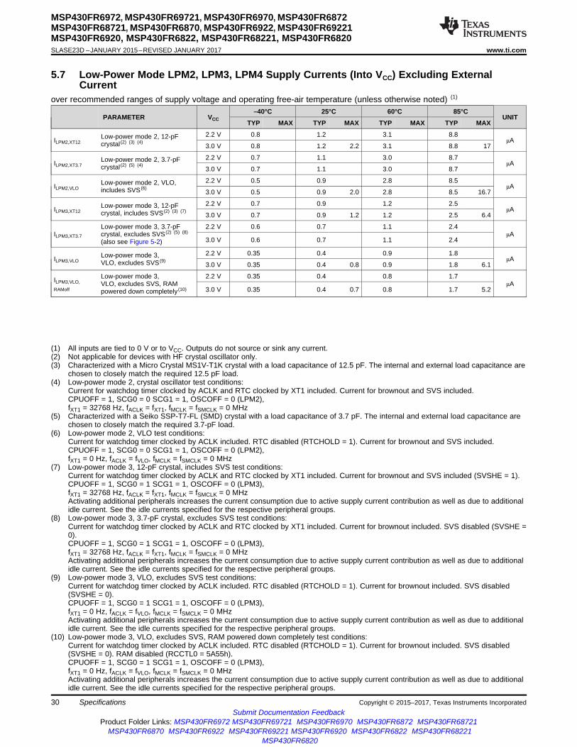
30
MSP430FR6972, MSP430FR69721, MSP430FR6970, MSP430FR6872MSP430FR68721, MSP430FR6870, MSP430FR6922, MSP430FR69221MSP430FR6920, MSP430FR6822, MSP430FR68221, MSP430FR6820SLASE23D –JANUARY 2015–REVISED JANUARY 2017 www.ti.com
Submit Documentation FeedbackProduct Folder Links: MSP430FR6972 MSP430FR69721 MSP430FR6970 MSP430FR6872 MSP430FR68721
MSP430FR6870 MSP430FR6922 MSP430FR69221 MSP430FR6920 MSP430FR6822 MSP430FR68221MSP430FR6820
Specifications Copyright © 2015–2017, Texas Instruments Incorporated
(1) All inputs are tied to 0 V or to VCC. Outputs do not source or sink any current.(2) Not applicable for devices with HF crystal oscillator only.(3) Characterized with a Micro Crystal MS1V-T1K crystal with a load capacitance of 12.5 pF. The internal and external load capacitance are
chosen to closely match the required 12.5 pF load.(4) Low-power mode 2, crystal oscillator test conditions:
Current for watchdog timer clocked by ACLK and RTC clocked by XT1 included. Current for brownout and SVS included.CPUOFF = 1, SCG0 = 0 SCG1 = 1, OSCOFF = 0 (LPM2),fXT1 = 32768 Hz, fACLK = fXT1, fMCLK = fSMCLK = 0 MHz
(5) Characterized with a Seiko SSP-T7-FL (SMD) crystal with a load capacitance of 3.7 pF. The internal and external load capacitance arechosen to closely match the required 3.7-pF load.
(6) Low-power mode 2, VLO test conditions:Current for watchdog timer clocked by ACLK included. RTC disabled (RTCHOLD = 1). Current for brownout and SVS included.CPUOFF = 1, SCG0 = 0 SCG1 = 1, OSCOFF = 0 (LPM2),fXT1 = 0 Hz, fACLK = fVLO, fMCLK = fSMCLK = 0 MHz
(7) Low-power mode 3, 12-pF crystal, includes SVS test conditions:Current for watchdog timer clocked by ACLK and RTC clocked by XT1 included. Current for brownout and SVS included (SVSHE = 1).CPUOFF = 1, SCG0 = 1 SCG1 = 1, OSCOFF = 0 (LPM3),fXT1 = 32768 Hz, fACLK = fXT1, fMCLK = fSMCLK = 0 MHzActivating additional peripherals increases the current consumption due to active supply current contribution as well as due to additionalidle current. See the idle currents specified for the respective peripheral groups.
(8) Low-power mode 3, 3.7-pF crystal, excludes SVS test conditions:Current for watchdog timer clocked by ACLK and RTC clocked by XT1 included. Current for brownout included. SVS disabled (SVSHE =0).CPUOFF = 1, SCG0 = 1 SCG1 = 1, OSCOFF = 0 (LPM3),fXT1 = 32768 Hz, fACLK = fXT1, fMCLK = fSMCLK = 0 MHzActivating additional peripherals increases the current consumption due to active supply current contribution as well as due to additionalidle current. See the idle currents specified for the respective peripheral groups.
(9) Low-power mode 3, VLO, excludes SVS test conditions:Current for watchdog timer clocked by ACLK included. RTC disabled (RTCHOLD = 1). Current for brownout included. SVS disabled(SVSHE = 0).CPUOFF = 1, SCG0 = 1 SCG1 = 1, OSCOFF = 0 (LPM3),fXT1 = 0 Hz, fACLK = fVLO, fMCLK = fSMCLK = 0 MHzActivating additional peripherals increases the current consumption due to active supply current contribution as well as due to additionalidle current. See the idle currents specified for the respective peripheral groups.
(10) Low-power mode 3, VLO, excludes SVS, RAM powered down completely test conditions:Current for watchdog timer clocked by ACLK included. RTC disabled (RTCHOLD = 1). Current for brownout included. SVS disabled(SVSHE = 0). RAM disabled (RCCTL0 = 5A55h).CPUOFF = 1, SCG0 = 1 SCG1 = 1, OSCOFF = 0 (LPM3),fXT1 = 0 Hz, fACLK = fVLO, fMCLK = fSMCLK = 0 MHzActivating additional peripherals increases the current consumption due to active supply current contribution as well as due to additionalidle current. See the idle currents specified for the respective peripheral groups.
5.7 Low-Power Mode LPM2, LPM3, LPM4 Supply Currents (Into VCC) Excluding ExternalCurrent
over recommended ranges of supply voltage and operating free-air temperature (unless otherwise noted) (1)
PARAMETER VCC–40°C 25°C 60°C 85°C
UNITTYP MAX TYP MAX TYP MAX TYP MAX
ILPM2,XT12Low-power mode 2, 12-pFcrystal (2) (3) (4)
2.2 V 0.8 1.2 3.1 8.8μA
3.0 V 0.8 1.2 2.2 3.1 8.8 17
ILPM2,XT3.7Low-power mode 2, 3.7-pFcrystal (2) (5) (4)
2.2 V 0.7 1.1 3.0 8.7μA
3.0 V 0.7 1.1 3.0 8.7
ILPM2,VLOLow-power mode 2, VLO,includes SVS (6)
2.2 V 0.5 0.9 2.8 8.5μA
3.0 V 0.5 0.9 2.0 2.8 8.5 16.7
ILPM3,XT12Low-power mode 3, 12-pFcrystal, includes SVS (2) (3) (7)
2.2 V 0.7 0.9 1.2 2.5μA
3.0 V 0.7 0.9 1.2 1.2 2.5 6.4
ILPM3,XT3.7
Low-power mode 3, 3.7-pFcrystal, excludes SVS (2) (5) (8)
(also see Figure 5-2)
2.2 V 0.6 0.7 1.1 2.4μA
3.0 V 0.6 0.7 1.1 2.4
ILPM3,VLOLow-power mode 3,VLO, excludes SVS (9)
2.2 V 0.35 0.4 0.9 1.8μA
3.0 V 0.35 0.4 0.8 0.9 1.8 6.1
ILPM3,VLO,RAMoff
Low-power mode 3,VLO, excludes SVS, RAMpowered down completely (10)
2.2 V 0.35 0.4 0.8 1.7μA
3.0 V 0.35 0.4 0.7 0.8 1.7 5.2

31
MSP430FR6972, MSP430FR69721, MSP430FR6970, MSP430FR6872MSP430FR68721, MSP430FR6870, MSP430FR6922, MSP430FR69221MSP430FR6920, MSP430FR6822, MSP430FR68221, MSP430FR6820
www.ti.com SLASE23D –JANUARY 2015–REVISED JANUARY 2017
Submit Documentation FeedbackProduct Folder Links: MSP430FR6972 MSP430FR69721 MSP430FR6970 MSP430FR6872 MSP430FR68721
MSP430FR6870 MSP430FR6922 MSP430FR69221 MSP430FR6920 MSP430FR6822 MSP430FR68221MSP430FR6820
SpecificationsCopyright © 2015–2017, Texas Instruments Incorporated
Low-Power Mode LPM2, LPM3, LPM4 Supply Currents (Into VCC) Excluding ExternalCurrent (continued)over recommended ranges of supply voltage and operating free-air temperature (unless otherwise noted) (1)
PARAMETER VCC–40°C 25°C 60°C 85°C
UNITTYP MAX TYP MAX TYP MAX TYP MAX
(11) Low-power mode 4, includes SVS test conditions:Current for brownout and SVS included (SVSHE = 1).CPUOFF = 1, SCG0 = 1 SCG1 = 1, OSCOFF = 1 (LPM4),fXT1 = 0 Hz, fACLK = 0 Hz, fMCLK = fSMCLK = 0 MHzActivating additional peripherals increases the current consumption due to active supply current contribution as well as due to additionalidle current. See the idle currents specified for the respective peripheral groups.
(12) Low-power mode 4, excludes SVS test conditions:Current for brownout included. SVS disabled (SVSHE = 0).CPUOFF = 1, SCG0 = 1 SCG1 = 1, OSCOFF = 1 (LPM4),fXT1 = 0 Hz, fACLK = 0 Hz, fMCLK = fSMCLK = 0 MHzActivating additional peripherals increases the current consumption due to active supply current contribution as well as due to additionalidle current. See the idle currents specified for the respective peripheral groups.
(13) Low-power mode 4, excludes SVS, RAM powered down completely test conditions:Current for brownout included. SVS disabled (SVSHE = 0). RAM disabled (RCCTL0 = 5A55h).CPUOFF = 1, SCG0 = 1 SCG1 = 1, OSCOFF = 1 (LPM4),fXT1 = 0 Hz, fACLK = 0 Hz, fMCLK = fSMCLK = 0 MHzActivating additional peripherals increases the current consumption due to active supply current contribution as well as due to additionalidle current. See the idle currents specified for the respective peripheral groups.
ILPM4,SVSLow-power mode 4, includesSVS (11)
2.2 V 0.45 0.55 0.9 1.8μA
3.0 V 0.45 0.55 0.8 0.9 1.8 6.2
ILPM4Low-power mode 4, excludesSVS (12)
2.2 V 0.25 0.4 0.7 1.6μA
3.0 V 0.25 0.4 0.65 0.7 1.6 4.6
ILPM4,RAMoff
Low-power mode 4, excludesSVS, RAM powered downcompletely (13)
2.2 V 0.25 0.4 0.7 1.4μA
3.0 V 0.25 0.4 0.65 0.7 1.4 4.6
IIDLE,GroupA
Additional idle current if one ormore modules from Group A(see Section 6.3.2) areactivated in LPM3 or LPM4
3.0 V 0.02 0.4 1.0 μA
IIDLE,GroupB
Additional idle current if one ormore modules from Group B(see Section 6.3.2) areactivated in LPM3 or LPM4
3.0 V 0.02 0.4 1.0 μA
IIDLE,GroupC
Additional idle current if one ormore modules from Group C(see Section 6.3.2) areactivated in LPM3 or LPM4
3.0 V 0.02 0.3 0.8 μA

32
MSP430FR6972, MSP430FR69721, MSP430FR6970, MSP430FR6872MSP430FR68721, MSP430FR6870, MSP430FR6922, MSP430FR69221MSP430FR6920, MSP430FR6822, MSP430FR68221, MSP430FR6820SLASE23D –JANUARY 2015–REVISED JANUARY 2017 www.ti.com
Submit Documentation FeedbackProduct Folder Links: MSP430FR6972 MSP430FR69721 MSP430FR6970 MSP430FR6872 MSP430FR68721
MSP430FR6870 MSP430FR6922 MSP430FR69221 MSP430FR6920 MSP430FR6822 MSP430FR68221MSP430FR6820
Specifications Copyright © 2015–2017, Texas Instruments Incorporated
(1) Current for watchdog timer clocked by ACLK and RTC clocked by XT1 included. Current for brownout included. SVS disabled(SVSHE = 0).CPUOFF = 1, SCG0 = 1 SCG1 = 1, OSCOFF = 0 (LPM3),fXT1 = 32768 Hz, fACLK = fXT1, fMCLK = fSMCLK = 0 MHzActivating additional peripherals increases the current consumption due to active supply current contribution as well as due to additionalidle current (idle current of Group containing LCD module already included). See the idle currents specified for the respective peripheralgroups.
(2) LCDMx = 11 (4-mux mode), LCDREXT = 1, LCDEXTBIAS = 1 (external biasing), LCD2B = 0 (1/3 bias), LCDCPEN = 0 (charge pumpdisabled), LCDSSEL = 0, LCDPREx = 101, LCDDIVx = 00011 (fLCD = 32768 Hz / 32 / 4 = 256 Hz)Current through external resistors not included (voltage levels are supplied by test equipment).Even segments S0, S2,... = 0, odd segments S1, S3,... = 1. No LCD panel load.
(3) LCDMx = 11 (4-mux mode), LCDREXT = 0, LCDEXTBIAS = 0 (internal biasing), LCD2B = 0 (1/3 bias), LCDCPEN = 0 (charge pumpdisabled), LCDSSEL = 0, LCDPREx = 101, LCDDIVx = 00011 (fLCD = 32768 Hz / 32 / 4 = 256 Hz)Even segments S0, S2,... = 0, odd segments S1, S3,... = 1. No LCD panel load.
(4) LCDMx = 11 (4-mux mode), LCDREXT = 0, LCDEXTBIAS = 0 (internal biasing), LCD2B = 0 (1/3 bias), LCDCPEN = 1 (charge pumpenabled), VLCDx = 1000 (VLCD= 3 V typ.), LCDSSEL = 0, LCDPREx = 101, LCDDIVx = 00011 (fLCD = 32768 Hz / 32 / 4 = 256 Hz)Even segments S0, S2,... = 0, odd segments S1, S3,... = 1. No LCD panel load. CLCDCAP = 10 µF
5.8 Low-Power Mode With LCD Supply Currents (Into VCC) Excluding External Currentover recommended ranges of supply voltage and operating free-air temperature (unless otherwise noted)
PARAMETER VCC
TEMPERATURE (TA)
UNIT–40°C 25°C 60°C 85°C
TYP MAX TYP MAX TYP MAX TYP MAX
ILPM3,XT12LCD,ext. bias
Low-power mode 3 (LPM3)current,12-pF crystal, LCD 4-mux mode, external biasing,excludes SVS (1) (2)
3.0 V 0.8 1.0 1.5 3.1 µA
ILPM3,XT12LCD,int. bias
Low-power mode 3 (LPM3)current, 12-pF crystal, LCD 4-mux mode, internal biasing,charge pump disabled,excludes SVS (1) (3)
3.0 V 2.5 2.7 3.4 2.8 4.4 9.3 µA
ILPM3,XT12LCD,CP
Low-power mode 3 (LPM3)current,12-pF crystal, LCD 4-mux mode, internal biasing,charge pump enabled, 1/3 bias,excludes SVS (1) (4)
2.2 V 6.2 6.4 7.0 8.0 µA
3.0 V 5.8 6.0 6.8 7.5 µA

33
MSP430FR6972, MSP430FR69721, MSP430FR6970, MSP430FR6872MSP430FR68721, MSP430FR6870, MSP430FR6922, MSP430FR69221MSP430FR6920, MSP430FR6822, MSP430FR68221, MSP430FR6820
www.ti.com SLASE23D –JANUARY 2015–REVISED JANUARY 2017
Submit Documentation FeedbackProduct Folder Links: MSP430FR6972 MSP430FR69721 MSP430FR6970 MSP430FR6872 MSP430FR68721
MSP430FR6870 MSP430FR6922 MSP430FR69221 MSP430FR6920 MSP430FR6822 MSP430FR68221MSP430FR6820
SpecificationsCopyright © 2015–2017, Texas Instruments Incorporated
(1) All inputs are tied to 0 V or to VCC. Outputs do not source or sink any current.(2) Not applicable for devices with HF crystal oscillator only.(3) Characterized with a Micro Crystal MS1V-T1K crystal with a load capacitance of 12.5 pF. The internal and external load capacitance are
chosen to closely match the required 12.5 pF load.(4) Low-power mode 3.5, 1-pF crystal including SVS test conditions:
Current for RTC clocked by XT1 included. Current for brownout and SVS included (SVSHE = 1). Core regulator disabled.PMMREGOFF = 1, CPUOFF = 1, SCG0 = 1 SCG1 = 1, OSCOFF = 1 (LPMx.5),fXT1 = 32768 Hz, fACLK = fXT1, fMCLK = fSMCLK = 0 MHz
(5) Characterized with a Seiko SSP-T7-FL (SMD) crystal with a load capacitance of 3.7 pF. The internal and external load capacitance arechosen to closely match the required 3.7-pF load.
(6) Low-power mode 3.5, 3.7-pF crystal excluding SVS test conditions:Current for RTC clocked by XT1 included.Current for brownout included. SVS disabled (SVSHE = 0). Core regulator disabled.PMMREGOFF = 1, CPUOFF = 1, SCG0 = 1 SCG1 = 1, OSCOFF = 1 (LPMx.5),fXT1 = 32768 Hz, fACLK = fXT1, fMCLK = fSMCLK = 0 MHz
(7) Low-power mode 4.5 including SVS test conditions:Current for brownout and SVS included (SVSHE = 1). Core regulator disabled.PMMREGOFF = 1, CPUOFF = 1, SCG0 = 1 SCG1 = 1, OSCOFF = 1 (LPMx.5),fXT1 = 0 Hz, fACLK = 0 Hz, fMCLK = fSMCLK = 0 MHz
(8) Low-power mode 4.5 excluding SVS test conditions:Current for brownout included. SVS disabled (SVSHE = 0). Core regulator disabled.PMMREGOFF = 1, CPUOFF = 1, SCG0 = 1 SCG1 = 1, OSCOFF = 1 (LPMx.5),fXT1 = 0 Hz, fACLK = 0 Hz, fMCLK = fSMCLK = 0 MHz
5.9 Low-Power Mode LPMx.5 Supply Currents (Into VCC) Excluding External Currentover recommended ranges of supply voltage and operating free-air temperature (unless otherwise noted) (1)
PARAMETER VCC–40°C 25°C 60°C 85°C
UNITTYP MAX TYP MAX TYP MAX TYP MAX
ILPM3.5,XT12Low-power mode 3.5, 12-pFcrystal including SVS (2) (3) (4)
2.2 V 0.45 0.5 0.6 0.75μA
3.0 V 0.45 0.5 0.75 0.6 0.75 1.4
ILPM3.5,XT3.7Low-power mode 3.5, 3.7-pFcrystal excluding SVS (2) (5) (6)
2.2 V 0.3 0.35 0.4 0.65μA
3.0 V 0.3 0.35 0.4 0.65
ILPM4.5,SVSLow-power mode 4.5, includingSVS (7)
2.2 V 0.2 0.3 0.35 0.4μA
3.0 V 0.2 0.3 0.5 0.35 0.4 0.7
ILPM4.5Low-power mode 4.5,excluding SVS (8)
2.2 V 0.03 0.04 0.06 0.14μA
3.0 V 0.03 0.04 0.06 0.14 0.5

0.2
0.3
0.4
0.5
0.6
0.7
-50.00 -25.00 0.00 25.00 50.00 75.00 100.00
LPM
3.5
Sup
ply
Cur
rent
[
A]
Temperature [C]
@ 3.0V, SVS off
@ 2.2V, SVS off
C003
0.00E+00
1.00E-01
2.00E-01
3.00E-01
4.00E-01
5.00E-01
6.00E-01
7.00E-01
-50 -25 0 25 50 75 100
LPM
.54
Sup
ply
Cur
rent
[
A]
Temperature [C]
@ 3.0V, SVS off
@ 2.2V, SVS off
@ 3.0V, SVS on
@ 2.2V, SVS on
C004
0
0.5
1
1.5
2
2.5
3
-50 -25 0 25 50 75 100
LPM
3 S
uppl
y C
urre
nt [
A]
Temperature [C]
@ 3.0V, SVS off
@ 2.2V, SVS off
@ 3.0V, SVS on
@ 2.2V, SVS on
C003
0
0.5
1
1.5
2
2.5
3
-50 -25 0 25 50 75 100
LPM
4 S
uppl
y C
urre
nt [
A]
Temperature [C]
@ 3.0V, SVS off
@ 2.2V, SVS off
@ 3.0V, SVS on
@ 2.2V, SVS on
C001
34
MSP430FR6972, MSP430FR69721, MSP430FR6970, MSP430FR6872MSP430FR68721, MSP430FR6870, MSP430FR6922, MSP430FR69221MSP430FR6920, MSP430FR6822, MSP430FR68221, MSP430FR6820SLASE23D –JANUARY 2015–REVISED JANUARY 2017 www.ti.com
Submit Documentation FeedbackProduct Folder Links: MSP430FR6972 MSP430FR69721 MSP430FR6970 MSP430FR6872 MSP430FR68721
MSP430FR6870 MSP430FR6922 MSP430FR69221 MSP430FR6920 MSP430FR6822 MSP430FR68221MSP430FR6820
Specifications Copyright © 2015–2017, Texas Instruments Incorporated
5.10 Typical Characteristics, Low-Power Mode Supply Currents
Figure 5-2. LPM3 Supply Current vs Temperature (LPM3,XT3.7) Figure 5-3. LPM4 Supply Current vs Temperature (LPM4,SVS)
Figure 5-4. LPM3.5 Supply Current vs Temperature(LPM3.5,XT3.7)
Figure 5-5. LPM4.5 Supply Current vs Temperature (LPM4.5)

35
MSP430FR6972, MSP430FR69721, MSP430FR6970, MSP430FR6872MSP430FR68721, MSP430FR6870, MSP430FR6922, MSP430FR69221MSP430FR6920, MSP430FR6822, MSP430FR68221, MSP430FR6820
www.ti.com SLASE23D –JANUARY 2015–REVISED JANUARY 2017
Submit Documentation FeedbackProduct Folder Links: MSP430FR6972 MSP430FR69721 MSP430FR6970 MSP430FR6872 MSP430FR68721
MSP430FR6870 MSP430FR6922 MSP430FR69221 MSP430FR6920 MSP430FR6822 MSP430FR68221MSP430FR6820
SpecificationsCopyright © 2015–2017, Texas Instruments Incorporated
(1) LCD_C: See Section 5.8. For other module currents not listed here, see the module specific parameter sections.
5.11 Typical Characteristics, Current Consumption per Module (1)
MODULE TEST CONDITIONS REFERENCE CLOCK MIN TYP MAX UNITTimer_A Module input clock 3 μA/MHzTimer_B Module input clock 5 μA/MHzeUSCI_A UART mode Module input clock 5.5 μA/MHzeUSCI_A SPI mode Module input clock 3.5 μA/MHzeUSCI_B SPI mode Module input clock 3.5 μA/MHzeUSCI_B I2C mode, 100 kbaud Module input clock 3.5 μA/MHzRTC_C 32 kHz 100 nAMPY Only from start to end of operation MCLK 25 μA/MHzAES Only from start to end of operation MCLK 21 μA/MHzCRC16 Only from start to end of operation MCLK 2.5 μA/MHzCRC32 Only from start to end of operation MCLK 2.5 μA/MHz
(1) N/A = not applicable(2) The junction-to-ambient thermal resistance under natural convection is obtained in a simulation on a JEDEC-standard, High-K board, as
specified in JESD51-7, in an environment described in JESD51-2a.(3) The junction-to-case (top) thermal resistance is obtained by simulating a cold plate test on the package top. No specific JEDEC-
standard test exists, but a close description can be found in the ANSI SEMI standard G30-88.(4) The junction-to-board thermal resistance is obtained by simulating in an environment with a ring cold plate fixture to control the PCB
temperature, as described in JESD51-8.(5) The junction-to-case (bottom) thermal resistance is obtained by simulating a cold plate test on the exposed (power) pad. No specific
JEDEC standard test exists, but a close description can be found in the ANSI SEMI standard G30-88.
5.12 Thermal Resistance Characteristics (1)
PARAMETER PACKAGE VALUE (1) UNITθJA Junction-to-ambient thermal resistance, still air (2)
TSSOP-56 (DGG)
57.7 °C/WθJC(TOP) Junction-to-case (top) thermal resistance (3) 15.1 °C/WθJB Junction-to-board thermal resistance (4) 26.5 °C/WΨJB Junction-to-board thermal characterization parameter 26.2 °C/WΨJT Junction-to-top thermal characterization parameter 0.5 °C/WθJC(BOTTOM) Junction-to-case (bottom) thermal resistance (5) N/A °C/WθJA Junction-to-ambient thermal resistance, still air (2)
QFP-64 (PN)
59.3 °C/WθJC(TOP) Junction-to-case (top) thermal resistance (3) 19.5 °C/WθJB Junction-to-board thermal resistance (4) 30.8 °C/WΨJB Junction-to-board thermal characterization parameter 30.5 °C/WΨJT Junction-to-top thermal characterization parameter 1.0 °C/WθJC(BOTTOM) Junction-to-case (bottom) thermal resistance (5) N/A °C/WθJA Junction-to-ambient thermal resistance, still air (2)
QFN-64 (RGC)
29.6 °C/WθJC(TOP) Junction-to-case (top) thermal resistance (3) 15.8 °C/WθJB Junction-to-board thermal resistance (4) 8.5 °C/WΨJB Junction-to-board thermal characterization parameter 8.5 °C/WΨJT Junction-to-top thermal characterization parameter 0.2 °C/WθJC(BOTTOM) Junction-to-case (bottom) thermal resistance (5) 1.2 °C/W

36
MSP430FR6972, MSP430FR69721, MSP430FR6970, MSP430FR6872MSP430FR68721, MSP430FR6870, MSP430FR6922, MSP430FR69221MSP430FR6920, MSP430FR6822, MSP430FR68221, MSP430FR6820SLASE23D –JANUARY 2015–REVISED JANUARY 2017 www.ti.com
Submit Documentation FeedbackProduct Folder Links: MSP430FR6972 MSP430FR69721 MSP430FR6970 MSP430FR6872 MSP430FR68721
MSP430FR6870 MSP430FR6922 MSP430FR69221 MSP430FR6920 MSP430FR6822 MSP430FR68221MSP430FR6820
Specifications Copyright © 2015–2017, Texas Instruments Incorporated
5.13 Timing and Switching Characteristics
5.13.1 Power Supply SequencingIt is recommended to power AVCC and DVCC pins from the same source. At a minimum, during powerup, power down, and device operation, the voltage difference between AVCC and DVCC must not exceedthe limits specified in Absolute Maximum Ratings. Exceeding the specified limits may cause malfunction ofthe device including erroneous writes to RAM and FRAM.
Table 5-1 lists the reset power ramp requirements.
(1) Fast supply voltage changes can trigger a BOR reset even within the recommended supply voltage range. To avoid unwanted BORresets, the supply voltage must change by less than 0.05 V per microsecond (±0.05 V/µs). Following the data sheet recommendation forcapacitor CDVCC should limit the slopes accordingly.
(2) The brownout levels are measured with a slowly changing supply.
Table 5-1. Brownout and Device Reset Power Ramp Requirementsover recommended ranges of supply voltage and operating free-air temperature (unless otherwise noted)
PARAMETER TEST CONDITIONS MIN MAX UNITVVCC_BOR– Brownout power-down level (1) | dDVCC/dt | < 3 V/s (2) 0.73 1.66 VVVCC_BOR+ Brownout power-up level (1) | dDVCC/dt | < 3 V/s (2) 0.79 1.68 V
Table 5-2 lists the characteristics of the SVS.
Table 5-2. SVSover recommended ranges of supply voltage and operating free-air temperature (unless otherwise noted)
PARAMETER TEST CONDITIONS MIN TYP MAX UNITISVSH,LPM SVSH current consumption, low power modes 170 300 nAVSVSH- SVSH power-down level 1.75 1.80 1.85 VVSVSH+ SVSH power-up level 1.77 1.88 1.99 VVSVSH_hys SVSH hysteresis 40 120 mVtPD,SVSH, AM SVSH propagation delay, active mode dVVcc/dt = –10 mV/µs 10 µs
5.13.2 Reset TimingTable 5-11 lists the required reset input timing.
(1) Not applicable if the RST/NMI pin is configured as NMI.
Table 5-3. Reset Inputover recommended ranges of supply voltage and operating free-air temperature (unless otherwise noted)
PARAMETER VCC MIN MAX UNITt(RST) External reset pulse duration on RST (1) 2.2 V, 3.0 V 2 µs

37
MSP430FR6972, MSP430FR69721, MSP430FR6970, MSP430FR6872MSP430FR68721, MSP430FR6870, MSP430FR6922, MSP430FR69221MSP430FR6920, MSP430FR6822, MSP430FR68221, MSP430FR6820
www.ti.com SLASE23D –JANUARY 2015–REVISED JANUARY 2017
Submit Documentation FeedbackProduct Folder Links: MSP430FR6972 MSP430FR69721 MSP430FR6970 MSP430FR6872 MSP430FR68721
MSP430FR6870 MSP430FR6922 MSP430FR69221 MSP430FR6920 MSP430FR6822 MSP430FR68221MSP430FR6820
SpecificationsCopyright © 2015–2017, Texas Instruments Incorporated
5.13.3 Clock Specifications
Table 5-4 lists the characteristics of the LFXT.
(1) To improve EMI on the LFXT oscillator, the following guidelines should be observed.• Keep the trace between the device and the crystal as short as possible.• Design a good ground plane around the oscillator pins.• Prevent crosstalk from other clock or data lines into oscillator pins LFXIN and LFXOUT.• Avoid running PCB traces underneath or adjacent to the LFXIN and LFXOUT pins.• Use assembly materials and processes that avoid any parasitic load on the oscillator LFXIN and LFXOUT pins.• If conformal coating is used, make sure that it does not induce capacitive or resistive leakage between the oscillator pins.
(2) When LFXTBYPASS is set, LFXT circuits are automatically powered down. Input signal is a digital square wave with parametricsdefined in the Schmitt-trigger Inputs section of this data sheet. Duty cycle requirements are defined by DCLFXT, SW.
(3) Maximum frequency of operation of the entire device cannot be exceeded.(4) Oscillation allowance is based on a safety factor of 5 for recommended crystals. The oscillation allowance is a function of the
LFXTDRIVE settings and the effective load. In general, comparable oscillator allowance can be achieved based on the followingguidelines, but should be evaluated based on the actual crystal selected for the application:• For LFXTDRIVE = 0, CL,eff = 3.7 pF• For LFXTDRIVE = 1, CL,eff = 6 pF• For LFXTDRIVE = 2, 6 pF ≤ CL,eff ≤ 9 pF• For LFXTDRIVE = 3, 9 pF ≤ CL,eff ≤ 12.5 pF
(5) This represents all the parasitic capacitance present at the LFXIN and LFXOUT terminals, respectively, including parasitic bond andpackage capacitance. The effective load capacitance, CL,eff can be computed as CIN x COUT / (CIN + COUT), where CIN and COUT is thetotal capacitance at the LFXIN and LFXOUT terminals, respectively.
(6) Requires external capacitors at both terminals. Values are specified by crystal manufacturers. Recommended values supported are 3.7pF, 6 pF, 9 pF, and 12.5 pF. Maximum shunt capacitance of 1.6 pF. The PCB adds additional capacitance, so it must also beconsidered in the overall capacitance. Verify that the recommended effective load capacitance of the selected crystal is met.
Table 5-4. Low-Frequency Crystal Oscillator, LFXT (1)
over recommended ranges of supply voltage and operating free-air temperature (unless otherwise noted)PARAMETER TEST CONDITIONS VCC MIN TYP MAX UNIT
IVCC.LFXT Current consumption
fOSC = 32768 Hz,LFXTBYPASS = 0, LFXTDRIVE = 0,TA = 25°C, CL,eff = 3.7 pF, ESR ≈ 44 kΩ
3.0 V 180
nA
fOSC = 32768 Hz,LFXTBYPASS = 0, LFXTDRIVE = 1,TA = 25°C, CL,eff = 6 pF, ESR ≈ 40 kΩ
3.0 V 185
fOSC = 32768 Hz,LFXTBYPASS = 0, LFXTDRIVE = 2,TA = 25°C, CL,eff = 9 pF, ESR ≈ 40 kΩ
3.0 V 225
fOSC = 32768 Hz,LFXTBYPASS = 0, LFXTDRIVE = 3,TA = 25°C, CL,eff = 12.5 pF, ESR ≈40 kΩ
3.0 V 330
fLFXTLFXT oscillator crystalfrequency LFXTBYPASS = 0 32768 Hz
DCLFXT LFXT oscillator duty cycle Measured at ACLK,fLFXT = 32768 Hz 30% 70%
fLFXT,SWLFXT oscillator logic-levelsquare-wave input frequency LFXTBYPASS = 1 (2) (3) 10.5 32.768 50 kHz
DCLFXT, SWLFXT oscillator logic-levelsquare-wave input duty cycle LFXTBYPASS = 1 30% 70%
OALFXTOscillation allowance forLF crystals (4)
LFXTBYPASS = 0, LFXTDRIVE = 1,fLFXT = 32768 Hz, CL,eff = 6 pF 210
kΩLFXTBYPASS = 0, LFXTDRIVE = 3,fLFXT = 32768 Hz, CL,eff = 12.5 pF 300
CLFXINIntegrated load capacitance atLFXIN terminal (5) (6) 2 pF
CLFXOUTIntegrated load capacitance atLFXOUT terminal (5) (6) 2 pF

38
MSP430FR6972, MSP430FR69721, MSP430FR6970, MSP430FR6872MSP430FR68721, MSP430FR6870, MSP430FR6922, MSP430FR69221MSP430FR6920, MSP430FR6822, MSP430FR68221, MSP430FR6820SLASE23D –JANUARY 2015–REVISED JANUARY 2017 www.ti.com
Submit Documentation FeedbackProduct Folder Links: MSP430FR6972 MSP430FR69721 MSP430FR6970 MSP430FR6872 MSP430FR68721
MSP430FR6870 MSP430FR6922 MSP430FR69221 MSP430FR6920 MSP430FR6822 MSP430FR68221MSP430FR6820
Specifications Copyright © 2015–2017, Texas Instruments Incorporated
Table 5-4. Low-Frequency Crystal Oscillator, LFXT(1) (continued)over recommended ranges of supply voltage and operating free-air temperature (unless otherwise noted)
PARAMETER TEST CONDITIONS VCC MIN TYP MAX UNIT
(7) Includes start-up counter of 1024 clock cycles.(8) Frequencies above the MAX specification do not set the fault flag. Frequencies between the MIN and MAX specification may set the
flag. A static condition or stuck at fault condition will set the flag.(9) Measured with logic-level input frequency but also applies to operation with crystals.
tSTART,LFXT Start-up time (7)
fOSC = 32768 Hz,LFXTBYPASS = 0, LFXTDRIVE = 0,TA = 25°C, CL,eff = 3.7 pF
3.0 V 800
msfOSC = 32768 HzLFXTBYPASS = 0, LFXTDRIVE = 3,TA = 25°C, CL,eff = 12.5 pF
3.0 V 1000
fFault,LFXT Oscillator fault frequency (8) (9) 0 3500 Hz
Table 5-5 lists the characteristics of the HFXT.
(1) To improve EMI on the HFXT oscillator the following guidelines should be observed.• Keep the traces between the device and the crystal as short as possible.• Design a good ground plane around the oscillator pins.• Prevent crosstalk from other clock or data lines into oscillator pins HFXIN and HFXOUT.• Avoid running PCB traces underneath or adjacent to the HFXIN and HFXOUT pins.• Use assembly materials and processes that avoid any parasitic load on the oscillator HFXIN and HFXOUT pins.• If conformal coating is used, ensure that it does not induce capacitive/resistive leakage between the oscillator pins.
(2) HFFREQ = 0 is not supported for HFXT crystal mode of operation.(3) Maximum frequency of operation of the entire device cannot be exceeded.
Table 5-5. High-Frequency Crystal Oscillator, HFXT (1)
over recommended ranges of supply voltage and operating free-air temperature (unless otherwise noted)PARAMETER TEST CONDITIONS VCC MIN TYP MAX UNIT
IDVCC.HFXTHFXT oscillator crystal current HFmode at typical ESR
fOSC = 4 MHz,HFXTBYPASS = 0, HFXTDRIVE = 0,HFFREQ = 1 (2),TA = 25°C,CL,eff = 18 pF, typical ESR, Cshunt
3.0 V
75
μA
fOSC = 8 MHz,HFXTBYPASS = 0, HFXTDRIVE = 1,HFFREQ = 1TA = 25°C,CL,eff = 18 pF, typical ESR, Cshunt
120
fOSC = 16 MHz,HFXTBYPASS = 0, HFXTDRIVE = 2,HFFREQ = 2,TA = 25°C,CL,eff = 18 pF, typical ESR, Cshunt
190
fOSC = 24 MHzHFXTBYPASS = 0, HFXTDRIVE = 3,HFFREQ = 3,TA = 25°C,CL,eff = 18 pF, typical ESR, Cshunt
250
fHFXTHFXT oscillator crystal frequency,crystal mode
HFXTBYPASS = 0, HFFREQ = 1 (2)(3) 4 8
MHzHFXTBYPASS = 0, HFFREQ = 2 (3) 8.01 16HFXTBYPASS = 0, HFFREQ = 3 (3) 16.01 24
DCHFXT HFXT oscillator duty cycle Measured at SMCLK,fHFXT = 16 MHz 40% 50% 60%

39
MSP430FR6972, MSP430FR69721, MSP430FR6970, MSP430FR6872MSP430FR68721, MSP430FR6870, MSP430FR6922, MSP430FR69221MSP430FR6920, MSP430FR6822, MSP430FR68221, MSP430FR6820
www.ti.com SLASE23D –JANUARY 2015–REVISED JANUARY 2017
Submit Documentation FeedbackProduct Folder Links: MSP430FR6972 MSP430FR69721 MSP430FR6970 MSP430FR6872 MSP430FR68721
MSP430FR6870 MSP430FR6922 MSP430FR69221 MSP430FR6920 MSP430FR6822 MSP430FR68221MSP430FR6820
SpecificationsCopyright © 2015–2017, Texas Instruments Incorporated
Table 5-5. High-Frequency Crystal Oscillator, HFXT(1) (continued)over recommended ranges of supply voltage and operating free-air temperature (unless otherwise noted)
PARAMETER TEST CONDITIONS VCC MIN TYP MAX UNIT
(4) When HFXTBYPASS is set, HFXT circuits are automatically powered down. Input signal is a digital square wave with parametricsdefined in the Schmitt-trigger Inputs section of this data sheet. Duty cycle requirements are defined by DCHFXT, SW.
(5) Oscillation allowance is based on a safety factor of 5 for recommended crystals.(6) Includes start-up counter of 1024 clock cycles.(7) This represents all the parasitic capacitance present at the HFXIN and HFXOUT terminals, respectively, including parasitic bond and
package capacitance. The effective load capacitance, CL,eff can be computed as CIN x COUT / (CIN + COUT), where CIN and COUT is thetotal capacitance at the HFXIN and HFXOUT terminals, respectively.
(8) Requires external capacitors at both terminals. Values are specified by crystal manufacturers. Recommended values supported are14 pF, 16 pF, and 18 pF. Maximum shunt capacitance of 7 pF. The PCB adds additional capacitance, so it must also be considered inthe overall capacitance. Verify that the recommended effective load capacitance of the selected crystal is met.
(9) Frequencies above the MAX specification do not set the fault flag. Frequencies between the MIN and MAX might set the flag. A staticcondition or stuck at fault condition will set the flag.
(10) Measured with logic-level input frequency but also applies to operation with crystals.
fHFXT,SW
HFXT oscillator logic-levelsquare-wave input frequency,bypass mode
HFXTBYPASS = 1, HFFREQ = 0 (4)(3) 0.9 4
MHz
HFXTBYPASS = 1, HFFREQ = 1 (4)(3) 4.01 8
HFXTBYPASS = 1, HFFREQ = 2 (4)(3) 8.01 16
HFXTBYPASS = 1, HFFREQ = 3 (4)(3) 16.01 24
DCHFXT,SW
HFXT oscillator logic-levelsquare-wave input duty cycle HFXTBYPASS = 1 40% 60%
OAHFXTOscillation allowance forHFXT crystals (5)
HFXTBYPASS = 0,HFXTDRIVE = 0, HFFREQ = 1 (2),fHFXT,HF = 4 MHz, CL,eff = 16 pF
450
Ω
HFXTBYPASS = 0,HFXTDRIVE = 1, HFFREQ = 1,fHFXT,HF = 8 MHz, CL,eff = 16 pF
320
HFXTBYPASS = 0,HFXTDRIVE = 2, HFFREQ = 2,fHFXT,HF = 16 MHz, CL,eff = 16 pF
200
HFXTBYPASS = 0,HFXTDRIVE = 3, HFFREQ = 3,fHFXT,HF = 24 MHz, CL,eff = 16 pF
200
tSTART,HFXT Start-up time (6)
fOSC = 4 MHz,HFXTBYPASS = 0, HFXTDRIVE = 0,HFFREQ = 1,TA = 25°C, CL,eff = 16 pF
3.0 V 1.6
msfOSC = 24 MHz,HFXTBYPASS = 0, HFXTDRIVE = 3,HFFREQ = 3,TA = 25°C, CL,eff = 16 pF
3.0 V 0.6
CHFXINIntegrated load capacitance atHFXIN terminaI (7) (8) 2 pF
CHFXOUTIntegrated load capacitance atHFXOUT terminaI (7) (8) 2 pF
fFault,HFXT Oscillator fault frequency (9) (10) 0 800 kHz

40
MSP430FR6972, MSP430FR69721, MSP430FR6970, MSP430FR6872MSP430FR68721, MSP430FR6870, MSP430FR6922, MSP430FR69221MSP430FR6920, MSP430FR6822, MSP430FR68221, MSP430FR6820SLASE23D –JANUARY 2015–REVISED JANUARY 2017 www.ti.com
Submit Documentation FeedbackProduct Folder Links: MSP430FR6972 MSP430FR69721 MSP430FR6970 MSP430FR6872 MSP430FR68721
MSP430FR6870 MSP430FR6922 MSP430FR69221 MSP430FR6920 MSP430FR6822 MSP430FR68221MSP430FR6820
Specifications Copyright © 2015–2017, Texas Instruments Incorporated
Table 5-6 lists the characteristics of the DCO.
(1) After a wakeup from LPM1, LPM2, LPM3 or LPM4, the DCO frequency fDCO might exceed the specified frequency range for a fewclocks cycles by up to 5% before settling into the specified steady state frequency range.
(2) Calculated using the box method: (MAX(–40°C to 85ºC) – MIN(–40°C to 85ºC)) / MIN(–40°C to 85ºC) / (85ºC – (–40ºC))
Table 5-6. DCOover recommended ranges of supply voltage and operating free-air temperature (unless otherwise noted)
PARAMETER TEST CONDITIONS VCC MIN TYP MAX UNIT
fDCO1DCO frequency range 1 MHz,trimmed
Measured at SMCLK, divide by 1,DCORSEL = 0, DCOFSEL = 0DCORSEL = 1, DCOFSEL = 0
1 ±3.5% MHz
fDCO2.7DCO frequency range 2.7 MHz,trimmed
Measured at SMCLK, divide by 1,DCORSEL = 0, DCOFSEL = 1 2.667 ±3.5% MHz
fDCO3.5DCO frequency range 3.5 MHz,trimmed
Measured at SMCLK, divide by 1,DCORSEL = 0, DCOFSEL = 2 3.5 ±3.5% MHz
fDCO4DCO frequency range 4 MHz,trimmed
Measured at SMCLK, divide by 1,DCORSEL = 0, DCOFSEL = 3 4 ±3.5% MHz
fDCO5.3DCO frequency range 5.3 MHz,trimmed
Measured at SMCLK, divide by 1,DCORSEL = 0, DCOFSEL = 4DCORSEL = 1, DCOFSEL = 1
5.333 ±3.5% MHz
fDCO7DCO frequency range 7 MHz,trimmed
Measured at SMCLK, divide by 1,DCORSEL = 0, DCOFSEL = 5DCORSEL = 1, DCOFSEL = 2
7 ±3.5% MHz
fDCO8DCO frequency range 8 MHz,trimmed
Measured at SMCLK, divide by 1,DCORSEL = 0, DCOFSEL = 6DCORSEL = 1, DCOFSEL = 3
8 ±3.5% MHz
fDCO16DCO frequency range 16 MHz,trimmed
Measured at SMCLK, divide by 1,DCORSEL = 1, DCOFSEL = 4 16 ±3.5% (1) MHz
fDCO21DCO frequency range 21 MHz,trimmed
Measured at SMCLK, divide by 2,DCORSEL = 1, DCOFSEL = 5 21 ±3.5% (1) MHz
fDCO24DCO frequency range 24 MHz,trimmed
Measured at SMCLK, divide by 2,DCORSEL = 1, DCOFSEL = 6 24 ±3.5% (1) MHz
fDCO,DC Duty cycle
Measured at SMCLK, divide by 1,No external divide, all DCORSEL andDCOFSEL settings except DCORSEL= 1, DCOFSEL = 5 and DCORSEL =1, DCOFSEL = 6
48% 50% 52%
tDCO,JITTER
DCO jitter
Based on fsignal = 10 kHz and DCOused for 12-bit SAR ADC samplingsource. This achieves >74-dB SNRdue to jitter; that is, it is limited byADC performance.
2 3 ns
dfDCO/dT DCO temperature drift (2) 3.0 V 0.01 %/ºC
Table 5-7 lists the characteristics of the VLO.
(1) Calculated using the box method: (MAX(–40°C to 85°C) – MIN(–40°C to 85°C)) / MIN(–40°C to 85°C) / (85°C – (–40°C))(2) Calculated using the box method: (MAX(1.8 V to 3.6 V) – MIN(1.8 V to 3.6 V)) / MIN(1.8 V to 3.6 V) / (3.6 V – 1.8 V)
Table 5-7. Internal Very-Low-Power Low-Frequency Oscillator (VLO)over recommended ranges of supply voltage and operating free-air temperature (unless otherwise noted)
PARAMETER TEST CONDITIONS VCC MIN TYP MAX UNITIVLO Current consumption 100 nAfVLO VLO frequency Measured at ACLK 6 9.4 14 kHzdfVLO/dT VLO frequency temperature drift Measured at ACLK (1) 0.2 %/°CdfVLO/dVCC VLO frequency supply voltage drift Measured at ACLK (2) 0.7 %/VfVLO,DC Duty cycle Measured at ACLK 40% 50% 60%

41
MSP430FR6972, MSP430FR69721, MSP430FR6970, MSP430FR6872MSP430FR68721, MSP430FR6870, MSP430FR6922, MSP430FR69221MSP430FR6920, MSP430FR6822, MSP430FR68221, MSP430FR6820
www.ti.com SLASE23D –JANUARY 2015–REVISED JANUARY 2017
Submit Documentation FeedbackProduct Folder Links: MSP430FR6972 MSP430FR69721 MSP430FR6970 MSP430FR6872 MSP430FR68721
MSP430FR6870 MSP430FR6922 MSP430FR69221 MSP430FR6920 MSP430FR6822 MSP430FR68221MSP430FR6820
SpecificationsCopyright © 2015–2017, Texas Instruments Incorporated
Table 5-8 lists the characteristics of the MODOSC.
(1) Calculated using the box method: (MAX(–40°C to 85°C) – MIN(–40°C to 85°C)) / MIN(–40°C to 85°C) / (85°C – (–40°C))(2) Calculated using the box method: (MAX(1.8 V to 3.6 V) – MIN(1.8 V to 3.6 V)) / MIN(1.8 V to 3.6 V) / (3.6 V – 1.8 V)
Table 5-8. Module Oscillator (MODOSC)over recommended ranges of supply voltage and operating free-air temperature (unless otherwise noted)
PARAMETER TEST CONDITIONS MIN TYP MAX UNITIMODOSC Current consumption Enabled 25 μAfMODOSC MODOSC frequency 4.0 4.8 5.4 MHzfMODOSC/dT MODOSC frequency temperature drift (1) 0.08 %/
fMODOSC/dVCCMODOSC frequency supply voltagedrift (2) 1.4 %/V
DCMODOSC Duty cycle Measured at SMCLK, divide by 1 40% 50% 60%

42
MSP430FR6972, MSP430FR69721, MSP430FR6970, MSP430FR6872MSP430FR68721, MSP430FR6870, MSP430FR6922, MSP430FR69221MSP430FR6920, MSP430FR6822, MSP430FR68221, MSP430FR6820SLASE23D –JANUARY 2015–REVISED JANUARY 2017 www.ti.com
Submit Documentation FeedbackProduct Folder Links: MSP430FR6972 MSP430FR69721 MSP430FR6970 MSP430FR6872 MSP430FR68721
MSP430FR6870 MSP430FR6922 MSP430FR69221 MSP430FR6920 MSP430FR6822 MSP430FR68221MSP430FR6820
Specifications Copyright © 2015–2017, Texas Instruments Incorporated
5.13.4 Wake-up Characteristics
Table 5-9 lists the device wake-up times.
(1) The wake-up time is measured from the edge of an external wake-up signal (for example, port interrupt or wake-up event) to the firstexternally observable MCLK clock edge with MCLKREQEN = 1. This time includes the activation of the FRAM during wakeup.
(2) With MCLKREQEN = 0, the MCLK is gated one additoinal one clock cycle (wake from LPM0, LPM1, LPM2, LPM3, and LPM4). Thedevice wake-up time is not affected by the status of the MCLKREQEN bit.
(3) The wake-up time is measured from the edge of an external wake-up signal (for example, port interrupt or wake-up event) until the firstinstruction of the user program is executed.
Table 5-9. Wake-up Times From Low-Power Modes and Resetover recommended ranges of supply voltage and operating free-air temperature (unless otherwise noted)
PARAMETER TESTCONDITIONS VCC MIN TYP MAX UNIT
tWAKE-UP FRAM
Additional wake-up time to activate the FRAMin AM if previously disabled by the FRAMcontroller or from an LPM if immediateactivation is selected
6 10 μs
tWAKE-UP LPM0 Wake-up time from LPM0 to active mode
MCLKREQEN = 1(1) 2.2 V, 3.0 V 400 ns +
1.5 / fDCO
MCLKREQEN = 0(1) (2) 2.2 V, 3.0 V 400 ns +
2.5 / fDCO
tWAKE-UP LPM1 Wake-up time from LPM1 to active mode (1) 2.2 V, 3.0 V 6 μstWAKE-UP LPM2 Wake-up time from LPM2 to active mode (1) 2.2 V, 3.0 V 6 μstWAKE-UP LPM3 Wake-up time from LPM3 to active mode (1) 2.2 V, 3.0 V 7 10 μstWAKE-UP LPM4 Wake-up time from LPM4 to active mode (1) 2.2 V, 3.0 V 7 10 μstWAKE-UP LPM3.5 Wake-up time from LPM3.5 to active mode (3) 2.2 V, 3.0 V 250 350 μs
tWAKE-UP LPM4.5 Wake-up time from LPM4.5 to active mode (3) SVSHE = 1 2.2 V, 3.0 V 250 350 μsSVSHE = 0 2.2 V, 3.0 V 0.4 0.8 ms
tWAKE-UP-RSTWake-up time from a RST pin triggered reset toactive mode (3) 2.2 V, 3.0 V 250 350 μs
tWAKE-UP-BOR Wake-up time from power-up to active mode (3) 2.2 V, 3.0 V 0.5 1.0 ms
Table 5-10 lists the typical charge required for wakeup.
(1) Charge used during the wake-up time from a given low-power mode to active mode. This does not include the energy required in activemode (for example, for an interrupt service routine).
(2) Charge required until start of user code. This does not include the energy required to reconfigure the device.
Table 5-10. Typical Wake-up Charge (1)
PARAMETER TEST CONDITIONS MIN TYP MAX UNIT
QWAKE-UP FRAMCharge used for activating the FRAM in AM or during wakeupfrom LPM0 if previously disabled by the FRAM controller. 15.1 nAs
QWAKE-UP LPM0Charge used to wake up from LPM0 to active mode (with FRAMactive) 4.4 nAs
QWAKE-UP LPM1Charge used to wake up from LPM1 to active mode (with FRAMactive) 15.1 nAs
QWAKE-UP LPM2Charge used to wake up from LPM2 to active mode (with FRAMactive) 15.3 nAs
QWAKE-UP LPM3Charge used to wake up from LPM3 to active mode (with FRAMactive) 16.5 nAs
QWAKE-UP LPM4Charge used to wake up from LPM4 to active mode (with FRAMactive) 16.5 nAs
QWAKE-UP LPM3.5 Charge used to wake up from LPM3.5 to active mode (2) 76 nAs
QWAKE-UP LPM4.5 Charge used to wake up from LPM4.5 to active mode (2) SVSHE = 1 77nAs
SVSHE = 0 77.5QWAKE-UP-RESET Charge used for reset from RST or BOR event to active mode (2) 75 nAs

0.10
1.00
10.00
100.00
1000.00
10000.00
0.001 0.01 0.1 1 10 100 1000 10000 100000
Avera
ge
Wake-u
pC
urr
ent (µ
A)
Wake-up Frequency (Hz)
LPM0
LPM1
LPM2,XT12
LPM3,XT12
LPM3.5,XT12
0.10
1.00
10.00
100.00
1000.00
10000.00
0.001 0.01 0.1 1 10 100 1000 10000 100000
Avera
ge
Wake-u
pC
urr
ent (µ
A)
Wake-up Frequency (Hz)
LPM0
LPM1
LPM2,XT12
LPM3,XT12
LPM3.5,XT12
43
MSP430FR6972, MSP430FR69721, MSP430FR6970, MSP430FR6872MSP430FR68721, MSP430FR6870, MSP430FR6922, MSP430FR69221MSP430FR6920, MSP430FR6822, MSP430FR68221, MSP430FR6820
www.ti.com SLASE23D –JANUARY 2015–REVISED JANUARY 2017
Submit Documentation FeedbackProduct Folder Links: MSP430FR6972 MSP430FR69721 MSP430FR6970 MSP430FR6872 MSP430FR68721
MSP430FR6870 MSP430FR6922 MSP430FR69221 MSP430FR6920 MSP430FR6822 MSP430FR68221MSP430FR6820
SpecificationsCopyright © 2015–2017, Texas Instruments Incorporated
5.13.4.1 Typical Characteristics, Average LPM Currents vs Wake-up Frequency
NOTE: The average wake-up current does not include the energy required in active mode; for example, for an interruptservice routine or to reconfigure the device.
Figure 5-6. Average LPM Currents vs Wake-up Frequency at 25°C
NOTE: The average wake-up current does not include the energy required in active mode; for example, for an interruptservice routine or to reconfigure the device.
Figure 5-7. Average LPM Currents vs Wake-up Frequency at 85°C

44
MSP430FR6972, MSP430FR69721, MSP430FR6970, MSP430FR6872MSP430FR68721, MSP430FR6870, MSP430FR6922, MSP430FR69221MSP430FR6920, MSP430FR6822, MSP430FR68221, MSP430FR6820SLASE23D –JANUARY 2015–REVISED JANUARY 2017 www.ti.com
Submit Documentation FeedbackProduct Folder Links: MSP430FR6972 MSP430FR69721 MSP430FR6970 MSP430FR6872 MSP430FR68721
MSP430FR6870 MSP430FR6922 MSP430FR69221 MSP430FR6920 MSP430FR6822 MSP430FR68221MSP430FR6820
Specifications Copyright © 2015–2017, Texas Instruments Incorporated
5.13.5 Digital I/Os
Table 5-11 lists the characteristics of the digital inputs.
(1) If the port pins PJ.4/LFXIN and PJ.5/LFXOUT are used as digital I/Os, they are connected by a 4-pF capacitor and a 35-MΩ resistor inseries. At frequencies of approximately 1 kHz and lower, the 4-pF capacitor can add to the pin capacitance of PJ.4/LFXIN andPJ.5/LFXOUT.
(2) The input leakage current is measured with VSS or VCC applied to the corresponding pins, unless otherwise noted.(3) The input leakage of the digital port pins is measured individually. The port pin is selected for input and the pullup or pulldown resistor is
disabled.(4) An external signal sets the interrupt flag every time the minimum interrupt pulse duration t(int) is met. It may be set by trigger signals
shorter than t(int).(5) Not applicable if the RST/NMI pin is configured as NMI.
Table 5-11. Digital Inputsover recommended ranges of supply voltage and operating free-air temperature (unless otherwise noted)
PARAMETER TEST CONDITIONS VCC MIN TYP MAX UNIT
VIT+ Positive-going input threshold voltage2.2 V 1.2 1.65
V3.0 V 1.65 2.25
VIT– Negative-going input threshold voltage2.2 V 0.55 1.00
V3.0 V 0.75 1.35
Vhys Input voltage hysteresis (VIT+ – VIT–)2.2 V 0.44 0.98
V3.0 V 0.60 1.30
RPull Pullup or pulldown resistor For pullup: VIN = VSSFor pulldown: VIN = VCC
20 35 50 kΩ
CI,dig Input capacitance, digital only port pins VIN = VSS or VCC 3 pF
CI,anaInput capacitance, port pins with shared analogfunctions (1) VIN = VSS or VCC 5 pF
Ilkg(Px.y) High-impedance input leakage current See (2) (3) 2.2 V,3.0 V –20 +20 nA
t(int)External interrupt timing (external trigger pulseduration to set interrupt flag) (4)
Ports with interrupt capability(see block diagram andterminal functiondescriptions).
2.2 V,3.0 V 20 ns
t(RST) External reset pulse duration on RST (5) 2.2 V,3.0 V 2 µs

45
MSP430FR6972, MSP430FR69721, MSP430FR6970, MSP430FR6872MSP430FR68721, MSP430FR6870, MSP430FR6922, MSP430FR69221MSP430FR6920, MSP430FR6822, MSP430FR68221, MSP430FR6820
www.ti.com SLASE23D –JANUARY 2015–REVISED JANUARY 2017
Submit Documentation FeedbackProduct Folder Links: MSP430FR6972 MSP430FR69721 MSP430FR6970 MSP430FR6872 MSP430FR68721
MSP430FR6870 MSP430FR6922 MSP430FR69221 MSP430FR6920 MSP430FR6822 MSP430FR68221MSP430FR6820
SpecificationsCopyright © 2015–2017, Texas Instruments Incorporated
Table 5-12 lists the characteristics of the digital outputs.
(1) The maximum total current, I(OHmax) and I(OLmax), for all outputs combined should not exceed ±48 mA to hold the maximum voltage dropspecified.
(2) The maximum total current, I(OHmax) and I(OLmax), for all outputs combined should not exceed ±100 mA to hold the maximum voltagedrop specified.
(3) The port can output frequencies at least up to the specified limit. It might support higher frequencies.(4) A resistive divider with 2 × R1 and R1 = 1.6 kΩ between VCC and VSS is used as load. The output is connected to the center tap of the
divider. CL = 20 pF is connected from the output to VSS.(5) The output voltage reaches at least 10% and 90% VCC at the specified toggle frequency.
Table 5-12. Digital Outputsover recommended ranges of supply voltage and operating free-air temperature (unless otherwise noted)
PARAMETER TEST CONDITIONS VCC MIN TYP MAX UNIT
VOH High-level output voltage
I(OHmax) = –1 mA (1)
2.2 V
VCC –0.25 VCC
VI(OHmax) = –3 mA (2) VCC –
0.60 VCC
I(OHmax) = –2 mA (1)
3.0 V
VCC –0.25 VCC
I(OHmax) = –6 mA (2) VCC –0.60 VCC
VOL Low-level output voltage
I(OLmax) = 1 mA (1)
2.2 VVSS
VSS +0.25
VI(OLmax) = 3 mA (2) VSS
VSS +0.60
I(OLmax) = 2 mA (1)
3.0 VVSS
VSS +0.25
I(OLmax) = 6 mA (2) VSSVSS +
0.60
fPx.y Port output frequency (with load) (3) CL = 20 pF, RL(4) (5) 2.2 V 16
MHz3.0 V 16
fPort_CLK Clock output frequency (3)ACLK, MCLK, or SMCLK atconfigured output portCL = 20 pF (5)
2.2 V 16MHz
3.0 V 16
trise,dig Port output rise time, digital only port pins CL = 20 pF2.2 V 4 15
ns3.0 V 3 15
tfall,dig Port output fall time, digital only port pins CL = 20 pF2.2 V 4 15
ns3.0 V 3 15
trise,anaPort output rise time, port pins with sharedanalog functions CL = 20 pF
2.2 V 6 15ns
3.0 V 4 15
tfall,anaPort output fall time, port pins with sharedanalog functions CL = 20 pF
2.2 V 6 15ns
3.0 V 4 15

-15
-10
-5
0
0 0.5 1 1.5 2
Hig
h-L
eve
lO
utp
ut
Cu
rre
nt
(mA
)
High-Level Output Voltage (V)
25°C
85°C
C001
P1.1-30
-20
-10
0
0 0.5 1 1.5 2 2.5 3
Hig
h-L
eve
lO
utp
ut
Cu
rre
nt
(mA
)
High-Level Output Voltage (V)
25°C
85°C
C001
P1.1
0
5
10
15
0 0.5 1 1.5 2
Low
-Level
Outp
ut
Curr
ent
(mA
)
Low-Level Output Voltage (V)
25°C
85°C
C001
P1.10
10
20
30
0 0.5 1 1.5 2 2.5 3
Low
-Level
Outp
ut
Curr
ent
(mA
)
Low-Level Output Voltage (V)
25°C
85°C
C001
P1.1
46
MSP430FR6972, MSP430FR69721, MSP430FR6970, MSP430FR6872MSP430FR68721, MSP430FR6870, MSP430FR6922, MSP430FR69221MSP430FR6920, MSP430FR6822, MSP430FR68221, MSP430FR6820SLASE23D –JANUARY 2015–REVISED JANUARY 2017 www.ti.com
Submit Documentation FeedbackProduct Folder Links: MSP430FR6972 MSP430FR69721 MSP430FR6970 MSP430FR6872 MSP430FR68721
MSP430FR6870 MSP430FR6922 MSP430FR69221 MSP430FR6920 MSP430FR6822 MSP430FR68221MSP430FR6820
Specifications Copyright © 2015–2017, Texas Instruments Incorporated
5.13.5.1 Typical Characteristics, Digital Outputs at 3.0 V and 2.2 V
VCC = 2.2 V
Figure 5-8. Typical Low-Level Output Current vs Low-LevelOutput Voltage
VCC = 3.0 V
Figure 5-9. Typical Low-Level Output Current vs Low-LevelOutput Voltage
VCC = 2.2 V
Figure 5-10. Typical High-Level Output Current vs High-LevelOutput Voltage
VCC = 3.0 V
Figure 5-11. Typical High-Level Output Current vs High-LevelOutput Voltage

100
1000
10 100
Pin
Osc
illat
or F
requ
ency
[kH
z]
External Load Capacitance (incl. board etc.) [pF]
fitted
25°C
85°C
C002
100
1000
10 100
Pin
Osc
illat
or F
requ
ency
[kH
z]
External Load Capacitance (incl. board etc.) [pF]
fitted
25°C
85°C
C002
47
MSP430FR6972, MSP430FR69721, MSP430FR6970, MSP430FR6872MSP430FR68721, MSP430FR6870, MSP430FR6922, MSP430FR69221MSP430FR6920, MSP430FR6822, MSP430FR68221, MSP430FR6820
www.ti.com SLASE23D –JANUARY 2015–REVISED JANUARY 2017
Submit Documentation FeedbackProduct Folder Links: MSP430FR6972 MSP430FR69721 MSP430FR6970 MSP430FR6872 MSP430FR68721
MSP430FR6870 MSP430FR6922 MSP430FR69221 MSP430FR6920 MSP430FR6822 MSP430FR68221MSP430FR6820
SpecificationsCopyright © 2015–2017, Texas Instruments Incorporated
Table 5-13 lists the characteristics of the pin oscillator.
(1) CL is the external load capacitance connected from the output to VSS and includes all parasitic effects such as PCB traces.
Table 5-13. Pin-Oscillator Frequency, Ports Pxover recommended ranges of supply voltage and operating free-air temperature (unless otherwise noted)
PARAMETER TEST CONDITIONS VCC MIN TYP MAX UNIT
foPx.y Pin-oscillator frequencyPx.y, CL = 10 pF (1) 3.0 V 1200 kHzPx.y, CL = 20 pF (1) 3.0 V 650 kHz
5.13.5.2 Typical Characteristics, Pin-Oscillator Frequency
VCC = 2.2 V One output active at a time.
Figure 5-12. Typical Oscillation Frequency vs Load Capacitance
VCC = 3.0 V One output active at a time.
Figure 5-13. Typical Oscillation Frequency vs Load Capacitance

48
MSP430FR6972, MSP430FR69721, MSP430FR6970, MSP430FR6872MSP430FR68721, MSP430FR6870, MSP430FR6922, MSP430FR69221MSP430FR6920, MSP430FR6822, MSP430FR68221, MSP430FR6820SLASE23D –JANUARY 2015–REVISED JANUARY 2017 www.ti.com
Submit Documentation FeedbackProduct Folder Links: MSP430FR6972 MSP430FR69721 MSP430FR6970 MSP430FR6872 MSP430FR68721
MSP430FR6870 MSP430FR6922 MSP430FR69221 MSP430FR6920 MSP430FR6822 MSP430FR68221MSP430FR6820
Specifications Copyright © 2015–2017, Texas Instruments Incorporated
5.13.6 Timer_A and Timer_B
Table 5-14 lists the characteristics of the Timer_A.
Table 5-14. Timer_Aover recommended ranges of supply voltage and operating free-air temperature (unless otherwise noted)
PARAMETER TEST CONDITIONS VCC MIN TYP MAX UNIT
fTA Timer_A input clock frequencyInternal: SMCLK or ACLK,External: TACLK,Duty cycle = 50% ±10%
2.2 V,3.0 V 16 MHz
tTA,cap Timer_A capture timing All capture inputs, minimum pulseduration required for capture
2.2 V,3.0 V 20 ns
Table 5-15 lists the characteristics of the Timer_B.
Table 5-15. Timer_Bover recommended ranges of supply voltage and operating free-air temperature (unless otherwise noted)
PARAMETER TEST CONDITIONS VCC MIN TYP MAX UNIT
fTB Timer_B input clock frequencyInternal: SMCLK or ACLK,External: TBCLK,Duty cycle = 50% ±10%
2.2 V,3.0 V 16 MHz
tTB,cap Timer_B capture timing All capture inputs, minimum pulseduration required for capture
2.2 V,3.0 V 20 ns

49
MSP430FR6972, MSP430FR69721, MSP430FR6970, MSP430FR6872MSP430FR68721, MSP430FR6870, MSP430FR6922, MSP430FR69221MSP430FR6920, MSP430FR6822, MSP430FR68221, MSP430FR6820
www.ti.com SLASE23D –JANUARY 2015–REVISED JANUARY 2017
Submit Documentation FeedbackProduct Folder Links: MSP430FR6972 MSP430FR69721 MSP430FR6970 MSP430FR6872 MSP430FR68721
MSP430FR6870 MSP430FR6922 MSP430FR69221 MSP430FR6920 MSP430FR6822 MSP430FR68221MSP430FR6820
SpecificationsCopyright © 2015–2017, Texas Instruments Incorporated
5.13.7 eUSCI
Table 5-16 lists the supported clock frequencies for the eUSCI in UART mode.
Table 5-16. eUSCI (UART Mode) Clock FrequencyPARAMETER CONDITIONS VCC MIN MAX UNIT
feUSCI eUSCI input clock frequencyInternal: SMCLK, ACLKExternal: UCLKDuty cycle = 50% ±10%
16 MHz
fBITCLKBITCLK clock frequency(equals baud rate in MBaud) 4 MHz
Table 5-17 lists the characteristics of the eUSCI in UART mode.
(1) Pulses on the UART receive input (UCxRX) that are shorter than the UART receive deglitch time are suppressed. Thus the selecteddeglitch time can limit the maximum usable baud rate. To make sure that pulses are correctly recognized, their duration should exceedthe maximum specification of the deglitch time.
Table 5-17. eUSCI (UART Mode)over recommended ranges of supply voltage and operating free-air temperature (unless otherwise noted)
PARAMETER TEST CONDITIONS VCC MIN TYP MAX UNIT
tt UART receive deglitch time (1)
UCGLITx = 0
2.2 V,3.0 V
5 30
nsUCGLITx = 1 20 90UCGLITx = 2 35 160UCGLITx = 3 50 220
Table 5-18 lists the supported clock frequencies for the eUSCI in SPI master mode.
Table 5-18. eUSCI (SPI Master Mode) Clock FrequencyPARAMETER CONDITIONS VCC MIN MAX UNIT
feUSCI eUSCI input clock frequency Internal: SMCLK, ACLKDuty cycle = 50% ±10% 16 MHz
Table 5-19 lists the characteristics of the eUSCI in SPI master mode.
(1) fUCxCLK = 1 / 2tLO/HI with tLO/HI = max(tVALID,MO(eUSCI) + tSU,SI(Slave), tSU,MI(eUSCI) + tVALID,SO(Slave)).For the slave parameters tSU,SI(Slave) and tVALID,SO(Slave), see the SPI parameters of the attached slave.
(2) Specifies the time to drive the next valid data to the SIMO output after the output changing UCLK clock edge. See the timing diagramsin Figure 5-14 and Figure 5-15.
Table 5-19. eUSCI (SPI Master Mode)over recommended ranges of supply voltage and operating free-air temperature (unless otherwise noted) (1)
PARAMETER TEST CONDITIONS VCC MIN TYP MAX UNITtSTE,LEAD STE lead time, STE active to clock UCSTEM = 1, UCMODEx = 01 or 10 1
UCxCLKcyclestSTE,LAG
STE lag time, last clock to STEinactive UCSTEM = 1, UCMODEx = 01 or 10 1
tSTE,ACCSTE access time, STE active toSIMO data out UCSTEM = 0, UCMODEx = 01 or 10 2.2 V,
3.0 V 60 ns
tSTE,DISSTE disable time, STE inactive toSOMI high impedance UCSTEM = 0, UCMODEx = 01 or 10 2.2 V,
3.0 V 80 ns
tSU,MI SOMI input data setup time2.2 V 40
ns3.0 V 40
tHD,MI SOMI input data hold time2.2 V 0
ns3.0 V 0
tVALID,MO SIMO output data valid time (2) UCLK edge to SIMO valid,CL = 20 pF
2.2 V 10ns
3.0 V 10

50
MSP430FR6972, MSP430FR69721, MSP430FR6970, MSP430FR6872MSP430FR68721, MSP430FR6870, MSP430FR6922, MSP430FR69221MSP430FR6920, MSP430FR6822, MSP430FR68221, MSP430FR6820SLASE23D –JANUARY 2015–REVISED JANUARY 2017 www.ti.com
Submit Documentation FeedbackProduct Folder Links: MSP430FR6972 MSP430FR69721 MSP430FR6970 MSP430FR6872 MSP430FR68721
MSP430FR6870 MSP430FR6922 MSP430FR69221 MSP430FR6920 MSP430FR6822 MSP430FR68221MSP430FR6820
Specifications Copyright © 2015–2017, Texas Instruments Incorporated
Table 5-19. eUSCI (SPI Master Mode) (continued)over recommended ranges of supply voltage and operating free-air temperature (unless otherwise noted)(1)
PARAMETER TEST CONDITIONS VCC MIN TYP MAX UNIT
(3) Specifies how long data on the SIMO output is valid after the output changing UCLK clock edge. Negative values indicate that the dataon the SIMO output can become invalid before the output changing clock edge observed on UCLK. See the timing diagrams in Figure 5-14 and Figure 5-15.
tHD,MO SIMO output data hold time (3) CL = 20 pF2.2 V 0
ns3.0 V 0

tSU,MI
tHD,MI
UCLK
SOMI
SIMO
tVALID,MO
CKPL = 0
CKPL = 1
tLOW/HIGH tLOW/HIGH
1/fUCxCLK
tSTE,LEAD tSTE,LAG
tSTE,ACC
UCMODEx = 01
UCMODEx = 10
STE
tHD,MO
tSTE,DIS
tSU,MI
tHD,MI
UCLK
SOMI
SIMO
tVALID,MO
CKPL = 0
CKPL = 1
tLOW/HIGH tLOW/HIGH
1/fUCxCLK
STE tSTE,LEAD tSTE,LAG
UCMODEx = 01
UCMODEx = 10
tHD,MO
tSTE,ACC tSTE,DIS
51
MSP430FR6972, MSP430FR69721, MSP430FR6970, MSP430FR6872MSP430FR68721, MSP430FR6870, MSP430FR6922, MSP430FR69221MSP430FR6920, MSP430FR6822, MSP430FR68221, MSP430FR6820
www.ti.com SLASE23D –JANUARY 2015–REVISED JANUARY 2017
Submit Documentation FeedbackProduct Folder Links: MSP430FR6972 MSP430FR69721 MSP430FR6970 MSP430FR6872 MSP430FR68721
MSP430FR6870 MSP430FR6922 MSP430FR69221 MSP430FR6920 MSP430FR6822 MSP430FR68221MSP430FR6820
SpecificationsCopyright © 2015–2017, Texas Instruments Incorporated
Figure 5-14. SPI Master Mode, CKPH = 0
Figure 5-15. SPI Master Mode, CKPH = 1

52
MSP430FR6972, MSP430FR69721, MSP430FR6970, MSP430FR6872MSP430FR68721, MSP430FR6870, MSP430FR6922, MSP430FR69221MSP430FR6920, MSP430FR6822, MSP430FR68221, MSP430FR6820SLASE23D –JANUARY 2015–REVISED JANUARY 2017 www.ti.com
Submit Documentation FeedbackProduct Folder Links: MSP430FR6972 MSP430FR69721 MSP430FR6970 MSP430FR6872 MSP430FR68721
MSP430FR6870 MSP430FR6922 MSP430FR69221 MSP430FR6920 MSP430FR6822 MSP430FR68221MSP430FR6820
Specifications Copyright © 2015–2017, Texas Instruments Incorporated
Table 5-20 lists the characteristics of the eUSCI in SPI slave mode.
(1) fUCxCLK = 1/2tLO/HI with tLO/HI ≥ max(tVALID,MO(Master) + tSU,SI(eUSCI), tSU,MI(Master) + tVALID,SO(eUSCI)).For the master parameters tSU,MI(Master) and tVALID,MO(Master) see the SPI parameters of the attached slave.
(2) Specifies the time to drive the next valid data to the SOMI output after the output changing UCLK clock edge. See the timing diagramsin Figure 5-16 and Figure 5-17.
(3) Specifies how long data on the SOMI output is valid after the output changing UCLK clock edge. See the timing diagrams in Figure 5-16and Figure 5-17.
Table 5-20. eUSCI (SPI Slave Mode)over recommended ranges of supply voltage and operating free-air temperature (unless otherwise noted) (1)
PARAMETER TEST CONDITIONS VCC MIN TYP MAX UNIT
tSTE,LEAD STE lead time, STE active to clock2.2 V 50
ns3.0 V 40
tSTE,LAG STE lag time, last clock to STE inactive2.2 V 2
ns3.0 V 3
tSTE,ACC STE access time, STE active to SOMI data out2.2 V 50
ns3.0 V 40
tSTE,DISSTE disable time, STE inactive to SOMI highimpedance
2.2 V 50ns
3.0 V 45
tSU,SI SIMO input data setup time2.2 V 4
ns3.0 V 4
tHD,SI SIMO input data hold time2.2 V 7
ns3.0 V 7
tVALID,SO SOMI output data valid time (2) UCLK edge to SOMI valid,CL = 20 pF
2.2 V 35ns
3.0 V 35
tHD,SO SOMI output data hold time (3) CL = 20 pF2.2 V 0
ns3.0 V 0

UCLK
CKPL = 0
CKPL = 1
SOMI
SIMO
tSU,SI
tHD,SI
tVALID,SO
tHD,SO
tLOW/HIGH
1/fUCxCLK
tLOW/HIGH
tSTE,DIStSTE,ACC
STE tSTE,LEAD tSTE,LAG
UCMODEx = 01
UCMODEx = 10
UCLK
CKPL = 0
CKPL = 1
SOMI
SIMO
tSU,SI
tHD,SI
tVALID,SO
tLOW/HIGH
1/fUCxCLK
tLOW/HIGH
tSTE,DIStSTE,ACC
STE tSTE,LEAD tSTE,LAG
UCMODEx = 01
UCMODEx = 10
tHD,SO
53
MSP430FR6972, MSP430FR69721, MSP430FR6970, MSP430FR6872MSP430FR68721, MSP430FR6870, MSP430FR6922, MSP430FR69221MSP430FR6920, MSP430FR6822, MSP430FR68221, MSP430FR6820
www.ti.com SLASE23D –JANUARY 2015–REVISED JANUARY 2017
Submit Documentation FeedbackProduct Folder Links: MSP430FR6972 MSP430FR69721 MSP430FR6970 MSP430FR6872 MSP430FR68721
MSP430FR6870 MSP430FR6922 MSP430FR69221 MSP430FR6920 MSP430FR6822 MSP430FR68221MSP430FR6820
SpecificationsCopyright © 2015–2017, Texas Instruments Incorporated
Figure 5-16. SPI Slave Mode, CKPH = 0
Figure 5-17. SPI Slave Mode, CKPH = 1

SDA
SCL
tHD,DAT
tSU,DAT
tHD,STA
tHIGHtLOW
tBUFtHD,STAtSU,STA
tSP
tSU,STO
54
MSP430FR6972, MSP430FR69721, MSP430FR6970, MSP430FR6872MSP430FR68721, MSP430FR6870, MSP430FR6922, MSP430FR69221MSP430FR6920, MSP430FR6822, MSP430FR68221, MSP430FR6820SLASE23D –JANUARY 2015–REVISED JANUARY 2017 www.ti.com
Submit Documentation FeedbackProduct Folder Links: MSP430FR6972 MSP430FR69721 MSP430FR6970 MSP430FR6872 MSP430FR68721
MSP430FR6870 MSP430FR6922 MSP430FR69221 MSP430FR6920 MSP430FR6822 MSP430FR68221MSP430FR6820
Specifications Copyright © 2015–2017, Texas Instruments Incorporated
Table 5-21 lists the characteristics of the eUSCI in I2C mode.
Table 5-21. eUSCI (I2C Mode)over recommended ranges of supply voltage and operating free-air temperature (unless otherwise noted) (see Figure 5-18)
PARAMETER TEST CONDITIONS VCC MIN TYP MAX UNIT
feUSCI eUSCI input clock frequencyInternal: SMCLK, ACLKExternal: UCLKDuty cycle = 50% ±10%
16 MHz
fSCL SCL clock frequency 2.2 V, 3.0 V 0 400 kHz
tHD,STA Hold time (repeated) STARTfSCL = 100 kHz
2.2 V, 3.0 V4.0
µsfSCL > 100 kHz 0.6
tSU,STA Setup time for a repeated STARTfSCL = 100 kHz
2.2 V, 3.0 V4.7
µsfSCL > 100 kHz 0.6
tHD,DAT Data hold time 2.2 V, 3.0 V 0 nstSU,DAT Data setup time 2.2 V, 3.0 V 100 ns
tSU,STO Setup time for STOPfSCL = 100 kHz
2.2 V, 3.0 V4.0
µsfSCL > 100 kHz 0.6
tBUFBus free time between a STOP andSTART condition
fSCL = 100 kHz 4.7us
fSCL > 100 kHz 1.3
tSPPulse duration of spikes suppressed byinput filter
UCGLITx = 0
2.2 V, 3.0 V
50 250
nsUCGLITx = 1 25 125UCGLITx = 2 12.5 62.5UCGLITx = 3 6.3 31.5
tTIMEOUT Clock low time-outUCCLTOx = 1
2.2 V, 3.0 V27
msUCCLTOx = 2 30UCCLTOx = 3 33
Figure 5-18. I2C Mode Timing
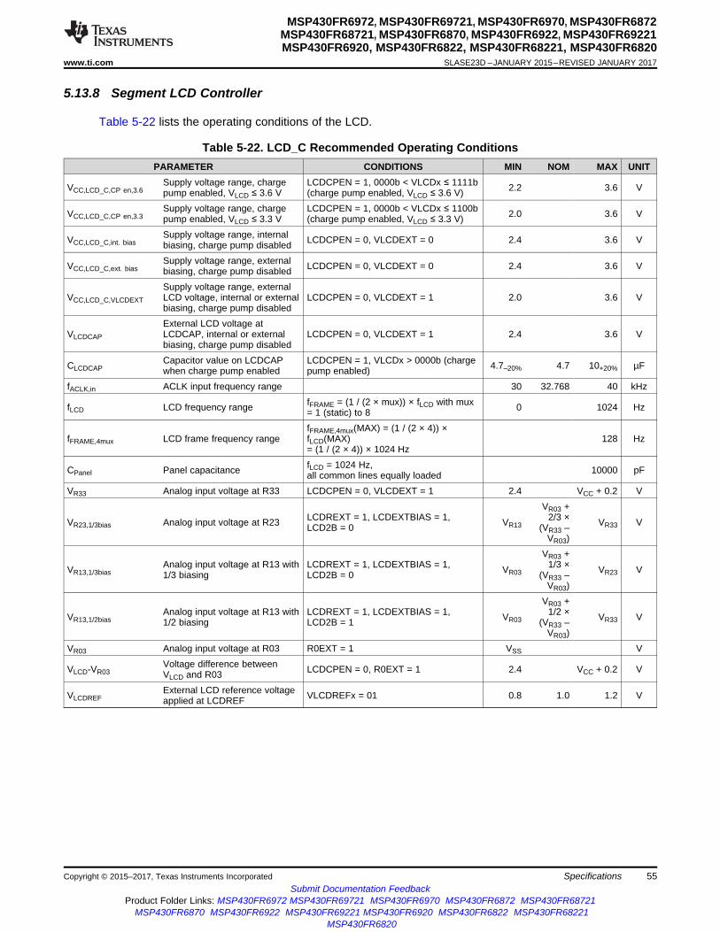
55
MSP430FR6972, MSP430FR69721, MSP430FR6970, MSP430FR6872MSP430FR68721, MSP430FR6870, MSP430FR6922, MSP430FR69221MSP430FR6920, MSP430FR6822, MSP430FR68221, MSP430FR6820
www.ti.com SLASE23D –JANUARY 2015–REVISED JANUARY 2017
Submit Documentation FeedbackProduct Folder Links: MSP430FR6972 MSP430FR69721 MSP430FR6970 MSP430FR6872 MSP430FR68721
MSP430FR6870 MSP430FR6922 MSP430FR69221 MSP430FR6920 MSP430FR6822 MSP430FR68221MSP430FR6820
SpecificationsCopyright © 2015–2017, Texas Instruments Incorporated
5.13.8 Segment LCD Controller
Table 5-22 lists the operating conditions of the LCD.
Table 5-22. LCD_C Recommended Operating ConditionsPARAMETER CONDITIONS MIN NOM MAX UNIT
VCC,LCD_C,CP en,3.6Supply voltage range, chargepump enabled, VLCD ≤ 3.6 V
LCDCPEN = 1, 0000b < VLCDx ≤ 1111b(charge pump enabled, VLCD ≤ 3.6 V) 2.2 3.6 V
VCC,LCD_C,CP en,3.3Supply voltage range, chargepump enabled, VLCD ≤ 3.3 V
LCDCPEN = 1, 0000b < VLCDx ≤ 1100b(charge pump enabled, VLCD ≤ 3.3 V) 2.0 3.6 V
VCC,LCD_C,int. biasSupply voltage range, internalbiasing, charge pump disabled LCDCPEN = 0, VLCDEXT = 0 2.4 3.6 V
VCC,LCD_C,ext. biasSupply voltage range, externalbiasing, charge pump disabled LCDCPEN = 0, VLCDEXT = 0 2.4 3.6 V
VCC,LCD_C,VLCDEXT
Supply voltage range, externalLCD voltage, internal or externalbiasing, charge pump disabled
LCDCPEN = 0, VLCDEXT = 1 2.0 3.6 V
VLCDCAP
External LCD voltage atLCDCAP, internal or externalbiasing, charge pump disabled
LCDCPEN = 0, VLCDEXT = 1 2.4 3.6 V
CLCDCAPCapacitor value on LCDCAPwhen charge pump enabled
LCDCPEN = 1, VLCDx > 0000b (chargepump enabled) 4.7–20% 4.7 10+20% µF
fACLK,in ACLK input frequency range 30 32.768 40 kHz
fLCD LCD frequency range fFRAME = (1 / (2 × mux)) × fLCD with mux= 1 (static) to 8 0 1024 Hz
fFRAME,4mux LCD frame frequency rangefFRAME,4mux(MAX) = (1 / (2 × 4)) ×fLCD(MAX)= (1 / (2 × 4)) × 1024 Hz
128 Hz
CPanel Panel capacitance fLCD = 1024 Hz,all common lines equally loaded 10000 pF
VR33 Analog input voltage at R33 LCDCPEN = 0, VLCDEXT = 1 2.4 VCC + 0.2 V
VR23,1/3bias Analog input voltage at R23 LCDREXT = 1, LCDEXTBIAS = 1,LCD2B = 0 VR13
VR03 +2/3 ×
(VR33 –VR03)
VR33 V
VR13,1/3biasAnalog input voltage at R13 with1/3 biasing
LCDREXT = 1, LCDEXTBIAS = 1,LCD2B = 0 VR03
VR03 +1/3 ×
(VR33 –VR03)
VR23 V
VR13,1/2biasAnalog input voltage at R13 with1/2 biasing
LCDREXT = 1, LCDEXTBIAS = 1,LCD2B = 1 VR03
VR03 +1/2 ×
(VR33 –VR03)
VR33 V
VR03 Analog input voltage at R03 R0EXT = 1 VSS V
VLCD-VR03Voltage difference betweenVLCD and R03 LCDCPEN = 0, R0EXT = 1 2.4 VCC + 0.2 V
VLCDREFExternal LCD reference voltageapplied at LCDREF VLCDREFx = 01 0.8 1.0 1.2 V

56
MSP430FR6972, MSP430FR69721, MSP430FR6970, MSP430FR6872MSP430FR68721, MSP430FR6870, MSP430FR6922, MSP430FR69221MSP430FR6920, MSP430FR6822, MSP430FR68221, MSP430FR6820SLASE23D –JANUARY 2015–REVISED JANUARY 2017 www.ti.com
Submit Documentation FeedbackProduct Folder Links: MSP430FR6972 MSP430FR69721 MSP430FR6970 MSP430FR6872 MSP430FR68721
MSP430FR6870 MSP430FR6922 MSP430FR69221 MSP430FR6920 MSP430FR6822 MSP430FR68221MSP430FR6820
Specifications Copyright © 2015–2017, Texas Instruments Incorporated
Table 5-23 lists the characteristics of the LCD.
Table 5-23. LCD_C Electrical Characteristicsover operating free-air temperature range (unless otherwise noted)
PARAMETER TEST CONDITIONS VCC MIN TYP MAX UNITVLCD,0
LCD voltage
VLCDx = 0000, VLCDEXT = 0 2.4 V to 3.6 V VCC
V
VLCD,1 LCDCPEN = 1, VLCDx = 0001b 2 V to 3.6 V 2.49 2.60 2.72VLCD,2 LCDCPEN = 1, VLCDx = 0010b 2 V to 3.6 V 2.66VLCD,3 LCDCPEN = 1, VLCDx = 0011b 2 V to 3.6 V 2.72VLCD,4 LCDCPEN = 1, VLCDx = 0100b 2 V to 3.6 V 2.78VLCD,5 LCDCPEN = 1, VLCDx = 0101b 2 V to 3.6 V 2.84VLCD,6 LCDCPEN = 1, VLCDx = 0110b 2 V to 3.6 V 2.90VLCD,7 LCDCPEN = 1, VLCDx = 0111b 2 V to 3.6 V 2.96VLCD,8 LCDCPEN = 1, VLCDx = 1000b 2 V to 3.6 V 3.02VLCD,9 LCDCPEN = 1, VLCDx = 1001b 2 V to 3.6 V 3.08VLCD,10 LCDCPEN = 1, VLCDx = 1010b 2 V to 3.6 V 3.14VLCD,11 LCDCPEN = 1, VLCDx = 1011b 2 V to 3.6 V 3.20VLCD,12 LCDCPEN = 1, VLCDx = 1100b 2 V to 3.6 V 3.26VLCD,13 LCDCPEN = 1, VLCDx = 1101b 2.2 V to 3.6 V 3.32VLCD,14 LCDCPEN = 1, VLCDx = 1110b 2.2 V to 3.6 V 3.38VLCD,15 LCDCPEN = 1, VLCDx = 1111b 2.2 V to 3.6 V 3.32 3.44 3.6
VLCD,7,0.8LCD voltage with externalreference of 0.8 V
LCDCPEN = 1, VLCDx = 0111b,VLCDREFx = 01b, VLCDREF = 0.8 V
2 V to 3.6 V 2.96 ×0.8 V V
VLCD,7,1.0LCD voltage with externalreference of 1.0 V
LCDCPEN = 1, VLCDx = 0111b,VLCDREFx = 01b, VLCDREF = 1.0 V
2 V to 3.6 V 2.96 ×1.0 V V
VLCD,7,1.2LCD voltage with externalreference of 1.2 V
LCDCPEN = 1, VLCDx = 0111b,VLCDREFx = 01b, VLCDREF = 1.2 V
2.2 V to 3.6 V 2.96 ×1.2 V V
ΔVLCDVoltage difference betweenconsecutive VLCDx settings
ΔVLCD = VLCD,x - VLCD,x–1with x = 0010b to 1111b 40 60 80 mV
ICC,Peak,CPPeak supply currents due tocharge pump activities
LCDCPEN = 1, VLCDx = 1111bexternal, with decoupling capacitor onDVCC supply ≥1 µF
2.2 V600 µA
tLCD,CP,onTime to charge CLCD whendischarged
CLCD = 4.7 µF, LCDCPEN = 0→1,VLCDx = 1111b
2.2 V 100 500 ms
ICP,LoadMaximum charge pump loadcurrent LCDCPEN = 1, VLCDx = 1111b 2.2 V 50 µA
RLCD,SegLCD driver output impedance,segment lines LCDCPEN = 0, ILOAD = ±10 µA 2.2 V 10 kΩ
RLCD,COMLCD driver output impedance,common lines LCDCPEN = 0, ILOAD = ±10 µA 2.2 V 10 kΩ

57
MSP430FR6972, MSP430FR69721, MSP430FR6970, MSP430FR6872MSP430FR68721, MSP430FR6870, MSP430FR6922, MSP430FR69221MSP430FR6920, MSP430FR6822, MSP430FR68221, MSP430FR6820
www.ti.com SLASE23D –JANUARY 2015–REVISED JANUARY 2017
Submit Documentation FeedbackProduct Folder Links: MSP430FR6972 MSP430FR69721 MSP430FR6970 MSP430FR6872 MSP430FR68721
MSP430FR6870 MSP430FR6922 MSP430FR69221 MSP430FR6920 MSP430FR6822 MSP430FR68221MSP430FR6820
SpecificationsCopyright © 2015–2017, Texas Instruments Incorporated
5.13.9 ADC12
Table 5-24 lists the power supply and input range conditions for the ADC.
(1) The analog input voltage range must be within the selected reference voltage range VR+ to VR– for valid conversion results.(2) The internal reference supply current is not included in current consumption parameter I(ADC12_B).(3) Typically about 60% of the total current into the AVCC and DVCC terminal is from AVCC.
Table 5-24. 12-Bit ADC, Power Supply and Input Range Conditionsover recommended ranges of supply voltage and operating free-air temperature (unless otherwise noted)
PARAMETER TEST CONDITIONS VCC MIN NOM MAX UNITV(Ax) Analog input voltage (1) All ADC12 analog input pins Ax 0 AVCC V
I(ADC12_B)single-ended mode
Operating supply current intoAVCC plus DVCC terminal (2) (3)
fADC12CLK = MODCLK, ADC12ON = 1,ADC12PWRMD = 0, ADC12DIF = 0REFON = 0, ADC12SHTx = 0,ADC12DIV = 0
3.0 V 145 199
µA2.2 V 140 190
I(ADC12_B)differentialmode
Operating supply current intoAVCC and DVCC terminals (2) (3)
fADC12CLK = MODCLK, ADC12ON = 1,ADC12PWRMD = 0, ADC12DIF = 1REFON = 0, ADC12SHTx = 0,ADC12DIV = 0
3.0 V 175 245
µA2.2 V 170 230
CI Input capacitance Only one terminal Ax can be selectedat one time 2.2 V 10 15 pF
RI Input MUX ON resistance 0 V ≤ V(Ax) ≤ AVCC>2 V 0.5 4
kΩ<2 V 1 10
Table 5-25 lists the timing parameter for the ADC.
(1) The ADC12OSC is sourced directly from MODOSC inside the UCS.(2) 14 × 1 / fADC12CLK. If ADC12WINC = 1, then 15 × 1 / fADC12CLK
(3) The condition is that the error in a conversion started after tADC12ON is less than ±0.5 LSB. The reference and input signals are alreadysettled.
Table 5-25. 12-Bit ADC, Timing Parametersover recommended ranges of supply voltage and operating free-air temperature (unless otherwise noted)
PARAMETER TEST CONDITIONS MIN TYP MAX UNIT
fADC12CLK Specified performance
For specified performance of ADC12 linearity parameterswith ADC12PWRMD = 0,If ADC12PWRMD = 1, the maximum is 1/4 of the valueshown here
0.45 5.4 MHz
fADC12CLK Reduced performance Linearity parameters have reduced performance 32.768 kHzfADC12OSC Internal oscillator (1) ADC12DIV = 0, fADC12CLK = fADC12OSC from MODCLK 4 4.8 5.4 MHz
tCONVERT Conversion time
REFON = 0, Internal oscillator,fADC12CLK = fADC12OSC from MODCLK,ADC12WINC = 0
2.6 3.5µs
External fADC12CLK from ACLK, MCLK, or SMCLK,ADC12SSEL ≠ 0
(2)
tADC12ONTurnon settling time ofthe ADC See (3) 100 ns
tADC12OFF
Time ADC must be offbefore can be turnedon again
tADC12OFF must be met to make sure tADC12ON time holds 100 ns

58
MSP430FR6972, MSP430FR69721, MSP430FR6970, MSP430FR6872MSP430FR68721, MSP430FR6870, MSP430FR6922, MSP430FR69221MSP430FR6920, MSP430FR6822, MSP430FR68221, MSP430FR6820SLASE23D –JANUARY 2015–REVISED JANUARY 2017 www.ti.com
Submit Documentation FeedbackProduct Folder Links: MSP430FR6972 MSP430FR69721 MSP430FR6970 MSP430FR6872 MSP430FR68721
MSP430FR6870 MSP430FR6922 MSP430FR69221 MSP430FR6920 MSP430FR6822 MSP430FR68221MSP430FR6820
Specifications Copyright © 2015–2017, Texas Instruments Incorporated
Table 5-25. 12-Bit ADC, Timing Parameters (continued)over recommended ranges of supply voltage and operating free-air temperature (unless otherwise noted)
PARAMETER TEST CONDITIONS MIN TYP MAX UNIT
(4) Approximately 10 Tau (τ) are needed to get an error of less than ±0.5 LSB: tsample = ln(2n+2) × (RS + RI) × (CI + Cpext), RS < 10 kΩ,where n = ADC resolution = 12, RS= external source resistance, Cpext = external parasitic capacitance.
(5) 6 × (1 / fADC12CLK)
tSample Sampling time RS = 400 Ω, RI = 4 kΩ,CI = 15 pF, Cpext= 8 pF (4)
All pulse sample mode(ADC12SHP = 1) andextended sample mode(ADC12SHP = 0) withbuffered reference (ADC12VRSEL = 0x1, 0x3, 0x5, 0x7,0x9, 0xB, 0xD, 0xF)
1 µs
Extended sample mode(ADC12SHP = 0) withunbuffered reference(ADC12 VRSEL= 0x0, 0x2,0x4, 0x6, 0xC, 0xE)
(5) µs
Table 5-26 lists the linearity parameters of the ADC when using an external reference.
(1) See Table 5-28 and Table 5-34 for more information on internal reference performance and see Designing With the MSP430FR59xxand MSP430FR58xx ADC for details on optimizing ADC performance for your application with the choice of internal versus externalreference.
(2) Offset is measured as the input voltage (at which ADC output transitions from 0 to 1) minus 0.5 LSB.(3) Offset increases as IR drop increases when VR– is AVSS.(4) For details, see the device descriptor table section in the MSP430FR58xx, MSP430FR59xx, MSP430FR68xx, and MSP430FR69xx
Family User's Guide.
Table 5-26. 12-Bit ADC, Linearity Parameters With External Reference (1)
over recommended ranges of supply voltage and operating free-air temperature (unless otherwise noted)PARAMETER TEST CONDITIONS MIN TYP MAX UNIT
Resolution Number of no missing codeoutput-code bits 12 bits
EIIntegral linearity error (INL)for differential input 1.2 V ≤ VR+ – VR–≤ AVCC ±1.8 LSB
EIIntegral linearity error (INL)for single ended inputs 1.2 V ≤ VR+ – VR–≤ AVCC ±2.2 LSB
EDDifferential linearity error(DNL) –0.99 +1.0 LSB
EO Offset error (2) (3) ADC12 VRSEL = 0x2 or 0x4 without TLV calibration,TLV calibration data can be used to improve the parameter (4) ±0.5 ±1.5 mV
EG,ext Gain error
With external voltage reference without internal buffer(ADC12 VRSEL = 0x2 or 0x4) without TLV calibration,TLV calibration data can be used to improve the parameter (4),VR+ = 2.5 V, VR– = AVSS
±0.8 ±2.5
LSBWith external voltage reference with internal buffer (ADC12VRSEL = 0x3),VR+ = 2.5 V, VR– = AVSS
±1 ±20
ET,ext Total unadjusted error
With external voltage reference without internal buffer(ADC12 VRSEL = 0x2 or 0x4) without TLV calibration,TLV calibration data can be used to improve the parameter (4),VR+ = 2.5 V, VR– = AVSS
±1.4 ±3.5
LSBWith external voltage reference with internal buffer (ADC12VRSEL = 0x3),VR+ = 2.5 V, VR– = AVSS
±1.4 ±21.0

59
MSP430FR6972, MSP430FR69721, MSP430FR6970, MSP430FR6872MSP430FR68721, MSP430FR6870, MSP430FR6922, MSP430FR69221MSP430FR6920, MSP430FR6822, MSP430FR68221, MSP430FR6820
www.ti.com SLASE23D –JANUARY 2015–REVISED JANUARY 2017
Submit Documentation FeedbackProduct Folder Links: MSP430FR6972 MSP430FR69721 MSP430FR6970 MSP430FR6872 MSP430FR68721
MSP430FR6870 MSP430FR6922 MSP430FR69221 MSP430FR6920 MSP430FR6822 MSP430FR68221MSP430FR6820
SpecificationsCopyright © 2015–2017, Texas Instruments Incorporated
Table 5-27 lists the differential dynamic performance characteristics of the ADC with an externalreference.
(1) See Table 5-28 and Table 5-34 for more information on internal reference performance and see Designing With the MSP430FR59xxand MSP430FR58xx ADC for details on optimizing ADC performance for your application with the choice of internal versus externalreference.
(2) ENOB = (SINAD – 1.76) / 6.02
Table 5-27. 12-Bit ADC, Dynamic Performance for Differential Inputs With External Reference (1)
over recommended ranges of supply voltage and operating free-air temperature (unless otherwise noted)PARAMETER TEST CONDITIONS MIN TYP MAX UNIT
SNR Signal-to-noise ratio VR+ = 2.5 V, VR– = AVSS 68 71 dBENOB Effective number of bits (2) VR+ = 2.5 V, VR– = AVSS 10.7 11.2 bits
Table 5-28 lists the differential dynamic performance characteristics of the ADC with an internal reference.
(1) See Table 5-34 for more information on internal reference performance and see Designing With the MSP430FR59xx andMSP430FR58xx ADC for details on optimizing ADC performance for your application with the choice of internal versus externalreference.
(2) ENOB = (SINAD – 1.76) / 6.02
Table 5-28. 12-Bit ADC, Dynamic Performance for Differential Inputs With Internal Reference (1)
over recommended ranges of supply voltage and operating free-air temperature (unless otherwise noted)PARAMETER TEST CONDITIONS MIN TYP MAX UNIT
ENOB Effective number of bits (2) VR+ = 2.5V, VR– = AVSS 10.3 10.7 Bits
Table 5-29 lists the single-ended dynamic performance characteristics of the ADC with an externalreference.
(1) See Table 5-30 and Table 5-34 for more information on internal reference performance and see Designing With the MSP430FR59xxand MSP430FR58xx ADC for details on optimizing ADC performance for your application with the choice of internal versus externalreference.
(2) ENOB = (SINAD – 1.76) / 6.02
Table 5-29. 12-Bit ADC, Dynamic Performance for Single-Ended Inputs With External Reference (1)
over recommended ranges of supply voltage and operating free-air temperature (unless otherwise noted)PARAMETER TEST CONDITIONS MIN TYP MAX UNIT
SNR Signal-to-noise ratio VR+ = 2.5 V, VR– = AVSS 64 68 dBENOB Effective number of bits (2) VR+ = 2.5 V, VR– = AVSS 10.2 10.7 bits
Table 5-30 lists the single-ended dynamic performance characteristics of the ADC with an internalreference.
(1) See Table 5-34 for more information on internal reference performance and see Designing With the MSP430FR59xx andMSP430FR58xx ADC for details on optimizing ADC performance for your application with the choice of internal versus externalreference.
(2) ENOB = (SINAD – 1.76) / 6.02
Table 5-30. 12-Bit ADC, Dynamic Performance for Single-Ended Inputs With Internal Reference (1)
over recommended ranges of supply voltage and operating free-air temperature (unless otherwise noted)PARAMETER TEST CONDITIONS MIN TYP MAX UNIT
ENOB Effective number of bits (2) VR+ = 2.5 V, VR– = AVSS 9.4 10.4 bits
Table 5-31 lists the dynamic performance characteristics of the ADC with using a 32.768-kHz clock.
(1) ENOB = (SINAD – 1.76) / 6.02
Table 5-31. 12-Bit ADC, Dynamic Performance With 32.768-kHz Clockover recommended ranges of supply voltage and operating free-air temperature (unless otherwise noted)
PARAMETER TEST CONDITIONS MIN TYP MAX UNIT
ENOB Effective number of bits (1) Reduced performance with fADC12CLK from ACLK LFXTat 32.768 kHz, VR+ = 2.5 V, VR– = AVSS 10 bits

500
550
600
650
700
750
800
850
900
950
–40 –20 0 20 40 60 80
Typ
ica
lTe
mp
era
ture
Se
nso
r V
olta
ge
(m
V)
Ambient Temperature (°C)
60
MSP430FR6972, MSP430FR69721, MSP430FR6970, MSP430FR6872MSP430FR68721, MSP430FR6870, MSP430FR6922, MSP430FR69221MSP430FR6920, MSP430FR6822, MSP430FR68221, MSP430FR6820SLASE23D –JANUARY 2015–REVISED JANUARY 2017 www.ti.com
Submit Documentation FeedbackProduct Folder Links: MSP430FR6972 MSP430FR69721 MSP430FR6970 MSP430FR6872 MSP430FR68721
MSP430FR6870 MSP430FR6922 MSP430FR69221 MSP430FR6920 MSP430FR6822 MSP430FR68221MSP430FR6820
Specifications Copyright © 2015–2017, Texas Instruments Incorporated
Table 5-32 lists the temperature sensor and built-in V1/2 characteristics.
(1) The temperature sensor offset can be as much as ±30°C. TI recommends a single-point calibration to minimize the offset error of thebuilt-in temperature sensor.
(2) The device descriptor structure contains calibration values for 30°C ±3°C and 85°C ±3°C for each of the available reference voltagelevels. The sensor voltage can be computed as VSENSE = TCSENSOR * (Temperature, °C) + VSENSOR, where TCSENSOR and VSENSOR canbe computed from the calibration values for higher accuracy.
(3) The typical equivalent impedance of the sensor is 250 kΩ. The sample time required includes the sensor on-time tSENSOR(on).(4) The on-time tV 1/2(on) is included in the sampling time tV 1/2 (sample); no additional on time is needed.
Table 5-32. 12-Bit ADC, Temperature Sensor and Built-In V1/2
over recommended ranges of supply voltage and operating free-air temperature (unless otherwise noted)PARAMETER TEST CONDITIONS VCC MIN TYP MAX UNIT
VSENSOR See (1) (2) ADC12ON = 1, ADC12TCMAP = 1,TA = 0°C (see Figure 5-19) 700 mV
TCSENSOR See (2) ADC12ON = 1, ADC12TCMAP = 1 2.5 mV/°C
tSENSOR(sample)
Sample time required ifADCTCMAP = 1 and channel(MAX – 1) is selected (3)
ADC12ON = 1, ADC12TCMAP = 1,Error of conversion result ≤ 1 LSB 30 µs
V1/2
AVCC voltage divider forADC12BATMAP = 1 on MAX inputchannel
ADC12ON = 1, ADC12BATMAP = 1 47.5% 50% 52.5%
IV 1/2current for battery monitor duringsample time ADC12ON = 1, ADC12BATMAP = 1 38 72 µA
tV 1/2 (sample)
Sample time required ifADC12BATMAP = 1 and channelMAX is selected (4)
ADC12ON = 1, ADC12BATMAP = 1 1.7 µs
Figure 5-19. Typical Temperature Sensor Voltage

61
MSP430FR6972, MSP430FR69721, MSP430FR6970, MSP430FR6872MSP430FR68721, MSP430FR6870, MSP430FR6922, MSP430FR69221MSP430FR6920, MSP430FR6822, MSP430FR68221, MSP430FR6820
www.ti.com SLASE23D –JANUARY 2015–REVISED JANUARY 2017
Submit Documentation FeedbackProduct Folder Links: MSP430FR6972 MSP430FR69721 MSP430FR6970 MSP430FR6872 MSP430FR68721
MSP430FR6870 MSP430FR6922 MSP430FR69221 MSP430FR6920 MSP430FR6822 MSP430FR68221MSP430FR6820
SpecificationsCopyright © 2015–2017, Texas Instruments Incorporated
Table 5-33 lists the external reference characteristics of the ADC.
(1) The external reference is used during ADC conversion to charge and discharge the capacitance array. The input capacitance, CI, is alsothe dynamic load for an external reference during conversion. The dynamic impedance of the reference supply should follow therecommendations on analog-source impedance to allow the charge to settle for 12-bit accuracy.
(2) Two decoupling capacitors, 10 µF and 470 nF, should be connected to VeREF to decouple the dynamic current required for an externalreference source if it is used for the ADC12_B. See also the MSP430FR58xx, MSP430FR59xx, MSP430FR68xx, and MSP430FR69xxFamily User's Guide.
Table 5-33. 12-Bit ADC, External Reference (1)
over recommended ranges of supply voltage and operating free-air temperature (unless otherwise noted)PARAMETER TEST CONDITIONS MIN MAX UNIT
VR+Positive external reference voltage inputVeREF+ or VeREF- based on ADC12 VRSEL bit VR+ > VR– 1.2 AVCC V
VR–Negative external reference voltage inputVeREF+ or VeREF- based on ADC12 VRSEL bit VR+ > VR– 0 1.2 V
(VR+ – VR–) Differential external reference voltage input VR+ > VR– 1.2 AVCC V
IVeREF+IVeREF-
Static input current singled ended input mode
1.2 V ≤ VeREF+≤ VAVCC, VeREF– = 0 VfADC12CLK = 5 MHz, ADC12SHTx = 1h,ADC12DIF = 0, ADC12PWRMD = 0
±10
µA1.2 V ≤ VeREF+≤ VAVCC , VeREF– = 0 VfADC12CLK = 5 MHz, ADC12SHTx = 8h,ADC12DIF = 0, ADC12PWRMD = 01
±2.5
IVeREF+IVeREF-
Static input current differential input mode
1.2 V ≤ VeREF+≤ VAVCC, VeREF– = 0 VfADC12CLK = 5 MHz, ADC12SHTx = 1h,ADC12DIF = 1, ADC12PWRMD = 0
±20
uA1.2 V ≤ VeREF+≤ VAVCC , VeREF– = 0 VfADC12CLK = 5 MHz, ADC12SHTx = 8h,ADC12DIF = 1, ADC12PWRMD = 1
±5
IVeREF+ Peak input current with single ended input 0 V ≤ VeREF+ ≤ VAVCC, ADC12DIF = 0 1.5 mAIVeREF+ Peak input current with differential input 0 V ≤ VeREF+ ≤ VAVCC, ADC12DIF = 1 3 mACVeREF+/- Capacitance at VeREF+ or VeREF- terminal See (2) 10 µF

62
MSP430FR6972, MSP430FR69721, MSP430FR6970, MSP430FR6872MSP430FR68721, MSP430FR6870, MSP430FR6922, MSP430FR69221MSP430FR6920, MSP430FR6822, MSP430FR68221, MSP430FR6820SLASE23D –JANUARY 2015–REVISED JANUARY 2017 www.ti.com
Submit Documentation FeedbackProduct Folder Links: MSP430FR6972 MSP430FR69721 MSP430FR6970 MSP430FR6872 MSP430FR68721
MSP430FR6870 MSP430FR6922 MSP430FR69221 MSP430FR6920 MSP430FR6822 MSP430FR68221MSP430FR6820
Specifications Copyright © 2015–2017, Texas Instruments Incorporated
5.13.10 REF Module
Table 5-34 lists the characteristics of the built-in voltage reference.
(1) Internal reference noise affects ADC performance when ADC uses internal reference. See Designing With the MSP430FR59xx andMSP430FR58xx ADC for details on optimizing ADC performance for your application with the choice of internal versus externalreference.
(2) Buffer offset affects ADC gain error and thus total unadjusted error.(3) The internal reference current is supplied through terminal AVCC.(4) Calculated using the box method: (MAX(–40°C to 85°C) – MIN(–40°C to 85°C)) / MIN(–40°C to 85°C)/(85°C – (–40°C)).(5) The condition is that the error in a conversion started after tREFON is less than ±0.5 LSB.
Table 5-34. REF, Built-In Referenceover recommended ranges of supply voltage and operating free-air temperature (unless otherwise noted)
PARAMETER TEST CONDITIONS VCC MIN TYP MAX UNIT
VREF+Positive built-in referencevoltage output
REFVSEL = 2 for 2.5 V, REFON = 1 2.7 V 2.5 ±1.5%VREFVSEL = 1 for 2.0 V, REFON = 1 2.2 V 2.0 ±1.5%
REFVSEL = 0 for 1.2 V, REFON = 1 1.8 V 1.2 ±1.8%Noise RMS noise at VREF (1) From 0.1 Hz to 10 Hz, REFVSEL = 0 110 600 µV
VOS_BUF_INTVREF ADC BUF_INT bufferoffset (2)
TA = 25°C , ADC ON, REFVSEL = 0,REFON = 1, REFOUT = 0 –12 +12 mV
VOS_BUF_EXTVREF ADC BUF_EXTbuffer offset (2)
TA = 25°C, REFVSEL = 0 , REFOUT = 1,REFON = 1 or ADC ON –12 +12 mV
AVCC(min)
AVCC minimum voltage,Positive built-in referenceactive
REFVSEL = 0 for 1.2 V 1.8VREFVSEL = 1 for 2.0 V 2.2
REFVSEL = 2 for 2.5 V 2.7
IREF+Operating supply currentinto AVCC terminal (3) REFON = 1 3 V 8 15 µA
IREF+_ADC_BUFOperating supply currentinto AVCC terminal (3)
ADC ON, REFOUT = 0, REFVSEL = 0, 1, 2,ADC12PWRMD = 0, 3 V 225 355
µA
ADC ON, REFOUT = 1, REFVSEL = 0, 1, 2,ADC12PWRMD = 0 3 V 1030 1660
ADC ON, REFOUT = 0, REFVSEL = 0, 1, 2,ADC12PWRMD = 1 3 V 120 185
ADC ON, REFOUT = 1, REFVSEL = 0, 1, 2,ADC12PWRMD = 1 3 V 545 895
ADC OFF, REFON = 1, REFOUT = 1,REFVSEL = 0, 1, 2 3 V 1085 1780
IO(VREF+)VREF maximum loadcurrent, VREF+ terminal
REFVSEL = 0, 1, 2, AVCC = AVCC(min) foreach reference level,REFON = REFOUT = 1
–1000 +10 µA
ΔVout/ΔIo(VREF+)
Load-current regulation,VREF+ terminal
REFVSEL = 0, 1, 2,IO(VREF+) = +10 µA or –1000 µA,AVCC = AVCC(min) for each reference level,REFON = REFOUT = 1
2500 µV/mA
CVREF+/-Capacitance at VREF+ andVREF- terminals REFON = REFOUT = 1 0 100 pF
TCREF+Temperature coefficient ofbuilt-in reference
REFVSEL = 0, 1, 2, REFON = REFOUT = 1,TA = –40°C to 85°C (4) 18 50 ppm/K
PSRR_DC Power supply rejection ratio(DC)
AVCC = AVCC(min) to AVCC(max), TA = 25°C,REFVSEL = 0, 1, 2, REFON = REFOUT = 1 120 400 µV/V
PSRR_AC Power supply rejection ratio(AC) dAVCC= 0.1 V at 1 kHz 3.0 mV/V
tSETTLESettling time of referencevoltage (5)
AVCC = AVCC (min) to AVCC(max),REFVSEL = 0, 1, 2, REFON = 0 → 1 75 80 µs

63
MSP430FR6972, MSP430FR69721, MSP430FR6970, MSP430FR6872MSP430FR68721, MSP430FR6870, MSP430FR6922, MSP430FR69221MSP430FR6920, MSP430FR6822, MSP430FR68221, MSP430FR6820
www.ti.com SLASE23D –JANUARY 2015–REVISED JANUARY 2017
Submit Documentation FeedbackProduct Folder Links: MSP430FR6972 MSP430FR69721 MSP430FR6970 MSP430FR6872 MSP430FR68721
MSP430FR6870 MSP430FR6922 MSP430FR69221 MSP430FR6920 MSP430FR6822 MSP430FR68221MSP430FR6820
SpecificationsCopyright © 2015–2017, Texas Instruments Incorporated
5.13.11 Comparator
Table 5-35 lists the characteristics of the comparator.
Table 5-35. Comparator_Eover recommended ranges of supply voltage and operating free-air temperature (unless otherwise noted)
PARAMETER TEST CONDITIONS VCC MIN TYP MAX UNIT
IAVCC_COMP
Comparator operating supplycurrent into AVCC, excludesreference resistor ladder
CEPWRMD = 00, CEON = 1,CERSx = 00 (fast)
2.2 V,3.0 V
11 20
µA
CEPWRMD = 01, CEON = 1,CERSx = 00 (medium) 9 17
CEPWRMD = 10, CEON = 1,CERSx = 00 (slow), TA = 30°C 0.5
CEPWRMD = 10, CEON = 1,CERSx = 00 (slow), TA = 85°C 1.3
IAVCC_REF
Quiescent current of resistorladder into AVCC, includingREF module current
CEREFLx = 01, CERSx = 10, REFON = 0,CEON = 0, CEREFACC = 0 2.2 V,
3.0 V
12 15µA
CEREFLx = 01, CERSx = 10, REFON = 0,CEON = 0, CEREFACC = 1 5 7
VREF Reference voltage level
CERSx = 11, CEREFLx = 01, CEREFACC = 0 1.8 V 1.17 1.2 1.23
V
CERSx = 11, CEREFLx = 10, CEREFACC = 0 2.2 V 1.92 2.0 2.08
CERSx = 11, CEREFLx = 11, CEREFACC = 0 2.7 V 2.40 2.5 2.60
CERSx = 11, CEREFLx = 01, CEREFACC = 1 1.8 V 1.10 1.2 1.245
CERSx = 11, CEREFLx = 10, CEREFACC = 1 2.2 V 1.90 2.0 2.08
CERSx = 11, CEREFLx = 11, CEREFACC = 1 2.7 V 2.35 2.5 2.60
VIC Common-mode input range 0 VCC-1 V
VOFFSET Input offset voltage
CEPWRMD = 00 –32 32
mVCEPWRMD = 01 –32 32
CEPWRMD = 10 –30 30
CIN Input capacitanceCEPWRMD = 00 or CEPWRMD = 01 9
pFCEPWRMD = 10 9
RSIN Series input resistanceOn (switch closed) 1 3 kΩ
Off (switch open) 50 MΩ
tPDPropagation delay, responsetime
CEPWRMD = 00, CEF = 0, Overdrive ≥ 20 mV 260 330ns
CEPWRMD = 01, CEF = 0, Overdrive ≥ 20 mV 350 460
CEPWRMD = 10, CEF = 0, Overdrive ≥ 20 mV 15 µs
tPD,filterPropagation delay with filteractive
CEPWRMD = 00 or 01, CEF = 1,Overdrive ≥ 20 mV, CEFDLY = 00 700 1000 ns
CEPWRMD = 00 or 01, CEF = 1,Overdrive ≥ 20 mV, CEFDLY = 01 1.0 1.8
µsCEPWRMD = 00 or 01, CEF = 1,Overdrive ≥ 20 mV, CEFDLY = 10 2.0 3.5
CEPWRMD = 00 or 01, CEF = 1,Overdrive ≥ 20 mV, CEFDLY = 11 4.0 7.0
tEN_CMP Comparator enable time
CEON = 0 → 1, VIN+, VIN- from pins,Overdrive ≥ 20 mV, CEPWRMD = 00 0.9 1.5
µsCEON = 0 → 1, VIN+, VIN- from pins,Overdrive ≥ 20 mV, CEPWRMD = 01 0.9 1.5
CEON = 0 → 1, VIN+, VIN- from pins,Overdrive ≥ 20 mV, CEPWRMD = 10 15 100
tEN_CMP_VREF
Comparator and referenceladder and reference voltageenable time
CEON = 0 → 1, CEREFLX = 10, CERSx = 10 or 11,CEREF0 = CEREF1 = 0x0F,Overdrive ≥ 20 mV
350 1500 µs
VCE_REFReference voltage for agiven tap
VIN = reference into resistor ladder,n = 0 to 31
VIN ×(n + 0.5)
/ 32
VIN ×(n + 1)
/ 32
VIN ×(n + 1.5)
/ 32V

64
MSP430FR6972, MSP430FR69721, MSP430FR6970, MSP430FR6872MSP430FR68721, MSP430FR6870, MSP430FR6922, MSP430FR69221MSP430FR6920, MSP430FR6822, MSP430FR68221, MSP430FR6820SLASE23D –JANUARY 2015–REVISED JANUARY 2017 www.ti.com
Submit Documentation FeedbackProduct Folder Links: MSP430FR6972 MSP430FR69721 MSP430FR6970 MSP430FR6872 MSP430FR68721
MSP430FR6870 MSP430FR6922 MSP430FR69221 MSP430FR6920 MSP430FR6822 MSP430FR68221MSP430FR6820
Specifications Copyright © 2015–2017, Texas Instruments Incorporated
5.13.12 FRAM Controller
Table 5-36 lists the characteristics of the FRAM.
(1) Writing to FRAM does not require a setup sequence or additional power when compared to reading from FRAM. The FRAM readcurrent IREAD is included in the active mode current consumption numbers IAM,FRAM.
(2) N/A = not applicable. FRAM does not require a special erase sequence.(3) Writing into FRAM is as fast as reading.(4) The maximum read (and write) speed is specified by fSYSTEM using the appropriate wait state settings (NWAITSx).
Table 5-36. FRAMover recommended ranges of supply voltage and operating free-air temperature (unless otherwise noted)
PARAMETER TESTCONDITIONS MIN TYP MAX UNIT
Read and write endurance 1015 cycles
tRetention Data retention durationTJ = 25°C 100
yearsTJ = 70°C 40TJ = 85°C 10
IWRITE Current to write into FRAM IREAD(1) nA
IERASE Erase current N/A (2) nAtWRITE Write time tREAD
(3) ns
tREADRead time, NWAITSx = 0 1 / fSYSTEM
(4)ns
Read time, NWAITSx = 1 2 / fSYSTEM(4)
5.13.13 Emulation and Debug
Table 5-37 lists the characteristics of the JTAG and Spy-Bi-Wire interface.
(1) Tools that access the Spy-Bi-Wire and BSL interfaces must wait for the tSBW,En time after the first transition of the TEST/SBWTCK pin(low to high), before the second transition of the pin (high to low) during the entry sequence.
(2) fTCK may be restricted to meet the timing requirements of the module selected.
Table 5-37. JTAG and Spy-Bi-Wire Interfaceover recommended ranges of supply voltage and operating free-air temperature (unless otherwise noted)
PARAMETER TESTCONDITIONS MIN TYP MAX UNIT
IJTAG Supply current adder when JTAG active (but not clocked) 2.2 V, 3.0 V 40 100 μAfSBW Spy-Bi-Wire input frequency 2.2 V, 3.0 V 0 10 MHztSBW,Low Spy-Bi-Wire low clock pulse duration 2.2 V, 3.0 V 0.04 15 μs
tSBW, EnSpy-Bi-Wire enable time (TEST high to acceptance of first clockedge) (1) 2.2 V, 3.0 V 110 μs
tSBW,Rst Spy-Bi-Wire return to normal operation time 15 100 μs
fTCK TCK input frequency, 4-wire JTAG (2) 2.2 V 0 16 MHz3.0 V 0 16 MHz
Rinternal Internal pulldown resistance on TEST 2.2 V, 3.0 V 20 35 50 kΩ
fTCLKTCLK/MCLK frequency during JTAG access, no FRAM access(limited by fSYSTEM) 16 MHz
tTCLK,Low/High TCLK low or high clock pulse duration, no FRAM access 25 ns
fTCLK,FRAMTCLK/MCLK frequency during JTAG access, including FRAM access(limited by fSYSTEM with no FRAM wait states) 4 MHz
tTCLK,FRAM,Low/High TCLK low or high clock pulse duration, including FRAM accesses 100 ns

65
MSP430FR6972, MSP430FR69721, MSP430FR6970, MSP430FR6872MSP430FR68721, MSP430FR6870, MSP430FR6922, MSP430FR69221MSP430FR6920, MSP430FR6822, MSP430FR68221, MSP430FR6820
www.ti.com SLASE23D –JANUARY 2015–REVISED JANUARY 2017
Submit Documentation FeedbackProduct Folder Links: MSP430FR6972 MSP430FR69721 MSP430FR6970 MSP430FR6872 MSP430FR68721
MSP430FR6870 MSP430FR6922 MSP430FR69221 MSP430FR6920 MSP430FR6822 MSP430FR68221MSP430FR6820
Detailed DescriptionCopyright © 2015–2017, Texas Instruments Incorporated
6 Detailed Description
6.1 OverviewThe Texas Instruments MSP430FR697x(1), MSP430FR687x(1), MSP430FR692x(1), andMSP430FR682x(1) family of ultra-low-power microcontrollers consists of several devices featuringdifferent sets of peripherals. The architecture, combined with seven low-power modes is optimized toachieve extended battery life for example in portable measurement applications. The devices features apowerful 16-bit RISC CPU, 16-bit registers, and constant generators that contribute to maximum codeefficiency. The devices are microcontroller configurations with up to five 16-bit timers, a comparator,eUSCIs that support UART, SPI, and I2C, a hardware multiplier, an AES accelerator, DMA, an RTCmodule with alarm capabilities, up to 52 I/O pins, and a high-performance 12-bit ADC. TheMSP430FR6xxx(1) devices also include an LCD module with contrast control for displays with up to 116segments.
6.2 CPUThe MSP430 CPU has a 16-bit RISC architecture that is highly transparent to the application. Alloperations, other than program-flow instructions, are performed as register operations in conjunction withseven addressing modes for source operand and four addressing modes for destination operand.
The CPU is integrated with 16 registers that provide reduced instruction execution time. The register-to-register operation execution time is one cycle of the CPU clock.
Four of the registers, R0 to R3, are dedicated as program counter, stack pointer, status register, andconstant generator, respectively. The remaining registers are general-purpose registers.
Peripherals are connected to the CPU using data, address, and control buses, and can be handled with allinstructions.
The instruction set consists of the original 51 instructions with three formats and seven address modesand additional instructions for the expanded address range. Each instruction can operate on word andbyte data. CPUxV2 can also operate on address-word data (20-bit).
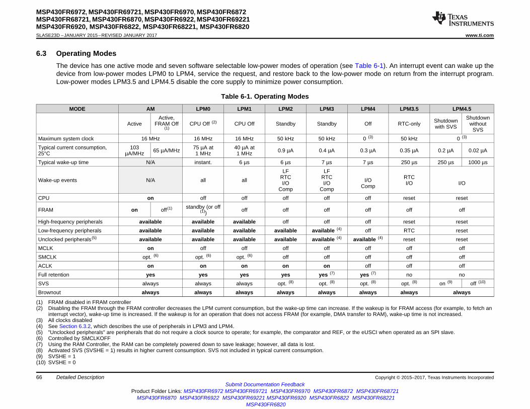
Copyright © 2015–2017, Texas Instruments IncorporatedDetailed DescriptionSubmit Documentation Feedback
Product Folder Links: MSP430FR6972 MSP430FR69721 MSP430FR6970 MSP430FR6872 MSP430FR68721MSP430FR6870 MSP430FR6922 MSP430FR69221 MSP430FR6920 MSP430FR6822 MSP430FR68221
MSP430FR6820
66
MSP430FR6972, MSP430FR69721, MSP430FR6970, MSP430FR6872MSP430FR68721, MSP430FR6870, MSP430FR6922, MSP430FR69221MSP430FR6920, MSP430FR6822, MSP430FR68221, MSP430FR6820SLASE23D –JANUARY 2015–REVISED JANUARY 2017 www.ti.com
6.3 Operating ModesThe device has one active mode and seven software selectable low-power modes of operation (see Table 6-1). An interrupt event can wake up thedevice from low-power modes LPM0 to LPM4, service the request, and restore back to the low-power mode on return from the interrupt program.Low-power modes LPM3.5 and LPM4.5 disable the core supply to minimize power consumption.
(1) FRAM disabled in FRAM controller(2) Disabling the FRAM through the FRAM controller decreases the LPM current consumption, but the wake-up time can increase. If the wakeup is for FRAM access (for example, to fetch an
interrupt vector), wake-up time is increased. If the wakeup is for an operation that does not access FRAM (for example, DMA transfer to RAM), wake-up time is not increased.(3) All clocks disabled(4) See Section 6.3.2, which describes the use of peripherals in LPM3 and LPM4.(5) "Unclocked peripherals" are peripherals that do not require a clock source to operate; for example, the comparator and REF, or the eUSCI when operated as an SPI slave.(6) Controlled by SMCLKOFF(7) Using the RAM Controller, the RAM can be completely powered down to save leakage; however, all data is lost.(8) Activated SVS (SVSHE = 1) results in higher current consumption. SVS not included in typical current consumption.(9) SVSHE = 1(10) SVSHE = 0
Table 6-1. Operating Modes
MODE AM LPM0 LPM1 LPM2 LPM3 LPM4 LPM3.5 LPM4.5
ActiveActive,
FRAM Off(1)
CPU Off (2) CPU Off Standby Standby Off RTC-only Shutdownwith SVS
Shutdownwithout
SVSMaximum system clock 16 MHz 16 MHz 16 MHz 50 kHz 50 kHz 0 (3) 50 kHz 0 (3)
Typical current consumption,25°C
103µA/MHz 65 µA/MHz 75 µA at
1 MHz40 µA at1 MHz 0.9 µA 0.4 µA 0.3 µA 0.35 µA 0.2 µA 0.02 µA
Typical wake-up time N/A instant. 6 µs 6 µs 7 µs 7 µs 250 µs 250 µs 1000 µs
Wake-up events N/A all all
LFRTCI/O
Comp
LFRTCI/O
Comp
_I/O
Comp
RTCI/O
_I/O
CPU on off off off off off reset reset
FRAM on off (1) standby (or off(1)) off off off off off off
High-frequency peripherals available available available off off off reset resetLow-frequency peripherals available available available available available (4) off RTC resetUnclocked peripherals (5) available available available available available (4) available (4) reset resetMCLK on off off off off off off offSMCLK opt. (6) opt. (6) opt. (6) off off off off offACLK on on on on on off off offFull retention yes yes yes yes yes (7) yes (7) no noSVS always always always opt. (8) opt. (8) opt. (8) opt. (8) on (9) off (10)
Brownout always always always always always always always always

67
MSP430FR6972, MSP430FR69721, MSP430FR6970, MSP430FR6872MSP430FR68721, MSP430FR6870, MSP430FR6922, MSP430FR69221MSP430FR6920, MSP430FR6822, MSP430FR68221, MSP430FR6820
www.ti.com SLASE23D –JANUARY 2015–REVISED JANUARY 2017
Submit Documentation FeedbackProduct Folder Links: MSP430FR6972 MSP430FR69721 MSP430FR6970 MSP430FR6872 MSP430FR68721
MSP430FR6870 MSP430FR6922 MSP430FR69221 MSP430FR6920 MSP430FR6822 MSP430FR68221MSP430FR6820
Detailed DescriptionCopyright © 2015–2017, Texas Instruments Incorporated
6.3.1 Peripherals in Low-Power ModesPeripherals can be in different states that affect which power mode the device can enter. The statesdepend on the operational modes of the peripherals (see Table 6-2). The states are:• A peripheral is in a "high-frequency state" if it requires or uses a clock with a "high" frequency of more
than 50 kHz.• A peripheral is in a "low-frequency state" if it requires or uses a clock with a "low" frequency of 50 kHz
or less.• A peripheral is in an "unclocked state" if it does not require or use an internal clock.
If the CPU requests a power mode that does not support the current state of all active peripherals, thedevice does not enter the requested power mode. The device instead enters a power mode that stillsupports the current state of the peripherals, except if an external clock is used. If an external clock isused, the application must use the correct frequency range for the requested power mode.
(1) Peripherals are in a state that requires or uses a clock with a "high" frequency of more than 50 kHz.(2) Peripherals are in a state that requires or uses a clock with a "low" frequency of 50 kHz or less.(3) Peripherals are in a state that does not require or does not use an internal clock.(4) The DMA always transfers data in active mode but can wait for a trigger in any low-power mode. A DMA trigger during a low-power
mode causes a temporary transition into active mode for the time of the transfer.(5) This peripheral operates during active mode only and delays the transition into a low-power mode until its operation is completed.
Table 6-2. Peripheral States
PERIPHERAL IN HIGH-FREQUENCY STATE (1) IN LOW-FREQUENCY STATE (2) IN UNCLOCKED STATE (3)
WDT Clocked by SMCLK Clocked by ACLK Not applicableDMA (4) Not applicable Not applicable Waiting for a triggerRTC_C Not applicable Clocked by LFXT Not applicableLCD_C Not applicable Clocked by ACLK or VLOCLK Not applicable
Timer_A TAx Clocked by SMCLK orclocked by external clock >50 kHz
Clocked by ACLK orclocked by external clock ≤50 kHz Clocked by external clock ≤50 kHz
Timer_B TBx Clocked by SMCLK orclocked by external clock >50 kHz
Clocked by ACLK orclocked by external clock ≤50 kHz Clocked by external clock ≤50 kHz
eUSCI_Ax inUART mode Clocked by SMCLK Clocked by ACLK Waiting for first edge of START bit.
eUSCI_Ax in SPImaster mode Clocked by SMCLK Clocked by ACLK Not applicable
eUSCI_Ax in SPIslave mode Clocked by external clock >50 kHz Clocked by external clock ≤50 kHz Clocked by external clock ≤50 kHz
eUSCI_Bx in I2Cmaster mode
Clocked by SMCLK orclocked by external clock >50 kHz
Clocked by ACLK orclocked by external clock ≤50 kHz Not applicable
eUSCI_Bx in I2Cslave mode Clocked by external clock >50 kHz Clocked by external clock ≤50 kHz Waiting for START condition or
clocked by external clock ≤50 kHzeUSCI_Bx in SPImaster mode Clocked by SMCLK Clocked by ACLK Not applicable
eUSCI_Bx in SPIslave mode Clocked by external clock >50 kHz Clocked by external clock ≤50 kHz Clocked by external clock ≤50 kHz
ADC12_B Clocked by SMCLK or by MODOSC Clocked by ACLK Waiting for a triggerREF_A Not applicable Not applicable AlwaysCOMP_E Not applicable Not applicable AlwaysCRC (5) Not applicable Not applicable Not applicableMPY (5) Not applicable Not applicable Not applicableAES (5) Not applicable Not applicable Not applicable

68
MSP430FR6972, MSP430FR69721, MSP430FR6970, MSP430FR6872MSP430FR68721, MSP430FR6870, MSP430FR6922, MSP430FR69221MSP430FR6920, MSP430FR6822, MSP430FR68221, MSP430FR6820SLASE23D –JANUARY 2015–REVISED JANUARY 2017 www.ti.com
Submit Documentation FeedbackProduct Folder Links: MSP430FR6972 MSP430FR69721 MSP430FR6970 MSP430FR6872 MSP430FR68721
MSP430FR6870 MSP430FR6922 MSP430FR69221 MSP430FR6920 MSP430FR6822 MSP430FR68221MSP430FR6820
Detailed Description Copyright © 2015–2017, Texas Instruments Incorporated
6.3.2 Idle Currents of Peripherals in LPM3 and LPM4Most peripherals can be activated to be operational in LPM3 if clocked by ACLK. Some modules are evenoperational in LPM4 because they do not require a clock to operate (for example, the comparator).Activating a peripheral in LPM3 or LPM4 increases the current consumption due to its active supplycurrent contribution but also due to an additional idle current. To limit the idle current adder, certainperipherals are group together. To achieve optimal current consumption, try to use modules within onegroup and to limit the number of groups with active modules. Table 6-3 lists the grouping. Modules notlisted in this table are either already included in the standard LPM3 current consumption specifications orcannot be used in LPM3 or LPM4.
The idle current adder is very small at room temperature (25°C) but increases at high temperatures(85°C); see the IIDLE current parameters in Section 5.7 for details.
Table 6-3. Peripheral Groups
Group A Group B Group CTimer TA0 Timer TA2 Timer TA3Timer TA1 Timer B0 eUSCI_A1
Comparator eUSCI_A0 LCD_CADC12_B eUSCI_B0
REF_A eUSCI_B1
6.4 Interrupt Vector Table and SignaturesThe interrupt vectors, the power-up start address, and signatures are in the address range 0FFFFh to0FF80h. Table 6-4 summarizes the content of this address range.
The power-up start address or reset vector is at 0FFFFh to 0FFFEh. It contains the 16-bit address pointingto the start address of the application program.
The interrupt vectors start at 0FFFDh extending to lower addresses. Each vector contains the 16-bitaddress of the appropriate interrupt-handler instruction sequence.
The vectors programmed into the address range from 0FFFFh to 0FFE0h are used as BSL password (ifenabled by the corresponding signature)
The signatures are at 0FF80h extending to higher addresses. Signatures are evaluated during devicestart-up. Starting from address 0FF88h extending to higher addresses a JTAG password canprogrammed. The password can extend into the interrupt vector locations using the interrupt vectoraddresses as additional bits for the password.
See the chapter System Resets, Interrupts, and Operating Modes, System Control Module (SYS) in theMSP430FR58xx, MSP430FR59xx, MSP430FR68xx, and MSP430FR69xx Family User's Guide for details.

69
MSP430FR6972, MSP430FR69721, MSP430FR6970, MSP430FR6872MSP430FR68721, MSP430FR6870, MSP430FR6922, MSP430FR69221MSP430FR6920, MSP430FR6822, MSP430FR68221, MSP430FR6820
www.ti.com SLASE23D –JANUARY 2015–REVISED JANUARY 2017
Submit Documentation FeedbackProduct Folder Links: MSP430FR6972 MSP430FR69721 MSP430FR6970 MSP430FR6872 MSP430FR68721
MSP430FR6870 MSP430FR6922 MSP430FR69221 MSP430FR6920 MSP430FR6822 MSP430FR68221MSP430FR6820
Detailed DescriptionCopyright © 2015–2017, Texas Instruments Incorporated
(1) Multiple source flags(2) A reset is generated if the CPU tries to fetch instructions from within peripheral space(3) (Non)maskable: the individual interrupt-enable bit can disable an interrupt event, but the general-interrupt enable cannot disable it.(4) Only on devices with ADC, otherwise reserved.
Table 6-4. Interrupt Sources, Flags, Vectors, and Signatures
INTERRUPT SOURCE INTERRUPT FLAG SYSTEMINTERRUPT
WORDADDRESS PRIORITY
System ResetPower-Up, Brownout, Supply
SupervisorExternal Reset RST
Watchdog Time-out (Watchdogmode)
WDT, FRCTL MPU, CS, PMMPassword Violation
FRAM uncorrectable bit errordetection
FRAM access time errorMPU segment violation
Software POR, BOR
SVSHIFGPMMRSTIFG
WDTIFGWDTPW, FRCTLPW, MPUPW, CSPW, PMMPW
UBDIFGACCTEIFG
MPUSEGIIFG, MPUSEG1IFG, MPUSEG2IFG,MPUSEG3IFG
PMMPORIFG, PMMBORIFG(SYSRSTIV) (1) (2)
Reset 0FFFEh Highest
System NMIVacant Memory Access
JTAG MailboxFRAM bit error detectionMPU segment violation
VMAIFGJMBNIFG, JMBOUTIFG
CBDIFG, UBDIFGMPUSEGIIFG, MPUSEG1IFG, MPUSEG2IFG,
MPUSEG3IFG(SYSSNIV) (1) (3)
(Non)maskable 0FFFCh
User NMIExternal NMI
Oscillator Fault
NMIIFG, OFIFG(SYSUNIV) (1) (3) (Non)maskable 0FFFAh
Comparator_E Comparator_E interrupt flags(CEIV) (1) Maskable 0FFF8h
Timer_B TB0 TB0CCR0.CCIFG Maskable 0FFF6h
Timer_B TB0TB0CCR1.CCIFG to TB0CCR6.CCIFG,
TB0CTL.TBIFG(TB0IV) (1)
Maskable 0FFF4h
Watchdog Timer(Interval Timer Mode) WDTIFG Maskable 0FFF2h
Reserved Reserved Maskable 0FFF0h
eUSCI_A0 Receive or Transmit
UCA0IFG: UCRXIFG, UCTXIFG (SPI mode)UCA0IFG:UCSTTIFG, UCTXCPTIFG, UCRXIFG,
UCTXIFG (UART mode)(UCA0IV) (1)
Maskable 0FFEEh
eUSCI_B0 Receive or Transmit
UCB0IFG: UCRXIFG, UCTXIFG (SPI mode)UCB0IFG: UCALIFG, UCNACKIFG, UCSTTIFG,UCSTPIFG, UCRXIFG0, UCTXIFG0, UCRXIFG1,UCTXIFG1, UCRXIFG2, UCTXIFG2, UCRXIFG3,UCTXIFG3, UCCNTIFG, UCBIT9IFG (I2C mode)
(UCB0IV) (1)
Maskable 0FFECh
ADC12_B
ADC12IFG0 to ADC12IFG31ADC12LOIFG, ADC12INIFG, ADC12HIIFG,
ADC12RDYIFG, ADC12OVIFG, ADC12TOVIFG(ADC12IV) (1) (4)
Maskable 0FFEAh
Timer_A TA0 TA0CCR0.CCIFG Maskable 0FFE8h
Timer_A TA0TA0CCR1.CCIFG to TA0CCR2.CCIFG,
TA0CTL.TAIFG(TA0IV) (1)
Maskable 0FFE6h
eUSCI_A1 Receive or Transmit
UCA1IFG:UCRXIFG, UCTXIFG (SPI mode)UCA1IFG:UCSTTIFG, UCTXCPTIFG, UCRXIFG,
UCTXIFG (UART mode)(UCA1IV) (1)
Maskable 0FFE4h
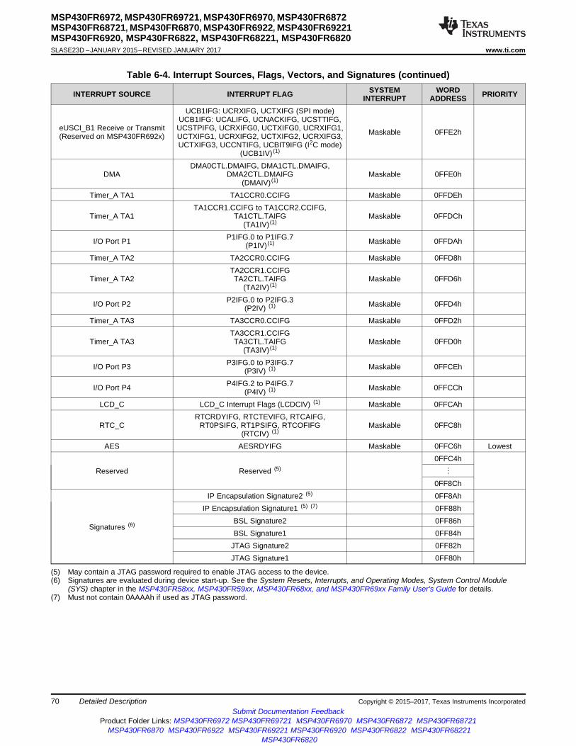
70
MSP430FR6972, MSP430FR69721, MSP430FR6970, MSP430FR6872MSP430FR68721, MSP430FR6870, MSP430FR6922, MSP430FR69221MSP430FR6920, MSP430FR6822, MSP430FR68221, MSP430FR6820SLASE23D –JANUARY 2015–REVISED JANUARY 2017 www.ti.com
Submit Documentation FeedbackProduct Folder Links: MSP430FR6972 MSP430FR69721 MSP430FR6970 MSP430FR6872 MSP430FR68721
MSP430FR6870 MSP430FR6922 MSP430FR69221 MSP430FR6920 MSP430FR6822 MSP430FR68221MSP430FR6820
Detailed Description Copyright © 2015–2017, Texas Instruments Incorporated
Table 6-4. Interrupt Sources, Flags, Vectors, and Signatures (continued)
INTERRUPT SOURCE INTERRUPT FLAG SYSTEMINTERRUPT
WORDADDRESS PRIORITY
(5) May contain a JTAG password required to enable JTAG access to the device.(6) Signatures are evaluated during device start-up. See the System Resets, Interrupts, and Operating Modes, System Control Module
(SYS) chapter in the MSP430FR58xx, MSP430FR59xx, MSP430FR68xx, and MSP430FR69xx Family User's Guide for details.(7) Must not contain 0AAAAh if used as JTAG password.
eUSCI_B1 Receive or Transmit(Reserved on MSP430FR692x)
UCB1IFG: UCRXIFG, UCTXIFG (SPI mode)UCB1IFG: UCALIFG, UCNACKIFG, UCSTTIFG,UCSTPIFG, UCRXIFG0, UCTXIFG0, UCRXIFG1,UCTXIFG1, UCRXIFG2, UCTXIFG2, UCRXIFG3,UCTXIFG3, UCCNTIFG, UCBIT9IFG (I2C mode)
(UCB1IV) (1)
Maskable 0FFE2h
DMADMA0CTL.DMAIFG, DMA1CTL.DMAIFG,
DMA2CTL.DMAIFG(DMAIV) (1)
Maskable 0FFE0h
Timer_A TA1 TA1CCR0.CCIFG Maskable 0FFDEh
Timer_A TA1TA1CCR1.CCIFG to TA1CCR2.CCIFG,
TA1CTL.TAIFG(TA1IV) (1)
Maskable 0FFDCh
I/O Port P1 P1IFG.0 to P1IFG.7(P1IV) (1) Maskable 0FFDAh
Timer_A TA2 TA2CCR0.CCIFG Maskable 0FFD8h
Timer_A TA2TA2CCR1.CCIFGTA2CTL.TAIFG
(TA2IV) (1)Maskable 0FFD6h
I/O Port P2 P2IFG.0 to P2IFG.3(P2IV) (1) Maskable 0FFD4h
Timer_A TA3 TA3CCR0.CCIFG Maskable 0FFD2h
Timer_A TA3TA3CCR1.CCIFGTA3CTL.TAIFG
(TA3IV) (1)Maskable 0FFD0h
I/O Port P3 P3IFG.0 to P3IFG.7(P3IV) (1) Maskable 0FFCEh
I/O Port P4 P4IFG.2 to P4IFG.7(P4IV) (1) Maskable 0FFCCh
LCD_C LCD_C Interrupt Flags (LCDCIV) (1) Maskable 0FFCAh
RTC_CRTCRDYIFG, RTCTEVIFG, RTCAIFG,
RT0PSIFG, RT1PSIFG, RTCOFIFG(RTCIV) (1)
Maskable 0FFC8h
AES AESRDYIFG Maskable 0FFC6h Lowest
Reserved Reserved (5)
0FFC4h⋮
0FF8Ch
Signatures (6)
IP Encapsulation Signature2 (5) 0FF8AhIP Encapsulation Signature1 (5) (7) 0FF88h
BSL Signature2 0FF86hBSL Signature1 0FF84h
JTAG Signature2 0FF82hJTAG Signature1 0FF80h
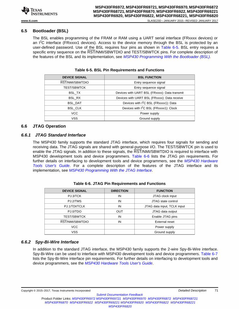
71
MSP430FR6972, MSP430FR69721, MSP430FR6970, MSP430FR6872MSP430FR68721, MSP430FR6870, MSP430FR6922, MSP430FR69221MSP430FR6920, MSP430FR6822, MSP430FR68221, MSP430FR6820
www.ti.com SLASE23D –JANUARY 2015–REVISED JANUARY 2017
Submit Documentation FeedbackProduct Folder Links: MSP430FR6972 MSP430FR69721 MSP430FR6970 MSP430FR6872 MSP430FR68721
MSP430FR6870 MSP430FR6922 MSP430FR69221 MSP430FR6920 MSP430FR6822 MSP430FR68221MSP430FR6820
Detailed DescriptionCopyright © 2015–2017, Texas Instruments Incorporated
6.5 Bootloader (BSL)The BSL enables programming of the FRAM or RAM using a UART serial interface (FRxxxx devices) oran I2C interface (FRxxxx1 devices). Access to the device memory through the BSL is protected by anuser-defined password. Use of the BSL requires four pins as shown in Table 6-5. BSL entry requires aspecific entry sequence on the RST/NMI/SBWTDIO and TEST/SBWTCK pins. For complete description ofthe features of the BSL and its implementation, see MSP430 Programming With the Bootloader (BSL).
Table 6-5. BSL Pin Requirements and Functions
DEVICE SIGNAL BSL FUNCTIONRST/NMI/SBWTDIO Entry sequence signal
TEST/SBWTCK Entry sequence signalBSL_TX Devices with UART BSL (FRxxxx): Data transmitBSL_RX Devices with UART BSL (FRxxxx): Data receive
BSL_DAT Devices with I2C BSL (FRxxxx1): DataBSL_CLK Devices with I2C BSL (FRxxxx1): Clock
VCC Power supplyVSS Ground supply
6.6 JTAG Operation
6.6.1 JTAG Standard InterfaceThe MSP430 family supports the standard JTAG interface, which requires four signals for sending andreceiving data. The JTAG signals are shared with general-purpose I/O. The TEST/SBWTCK pin is used toenable the JTAG signals. In addition to these signals, the RST/NMI/SBWTDIO is required to interface withMSP430 development tools and device programmers. Table 6-6 lists the JTAG pin requirements. Forfurther details on interfacing to development tools and device programmers, see the MSP430 HardwareTools User's Guide. For a complete description of the features of the JTAG interface and itsimplementation, see MSP430 Programming With the JTAG Interface.
Table 6-6. JTAG Pin Requirements and Functions
DEVICE SIGNAL DIRECTION FUNCTIONPJ.3/TCK IN JTAG clock inputPJ.2/TMS IN JTAG state control
PJ.1/TDI/TCLK IN JTAG data input, TCLK inputPJ.0/TDO OUT JTAG data output
TEST/SBWTCK IN Enable JTAG pinsRST/NMI/SBWTDIO IN External reset
VCC Power supplyVSS Ground supply
6.6.2 Spy-Bi-Wire InterfaceIn addition to the standard JTAG interface, the MSP430 family supports the 2-wire Spy-Bi-Wire interface.Spy-Bi-Wire can be used to interface with MSP430 development tools and device programmers. Table 6-7lists the Spy-Bi-Wire interface pin requirements. For further details on interfacing to development tools anddevice programmers, see the MSP430 Hardware Tools User's Guide.
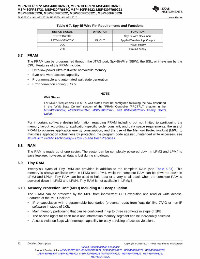
72
MSP430FR6972, MSP430FR69721, MSP430FR6970, MSP430FR6872MSP430FR68721, MSP430FR6870, MSP430FR6922, MSP430FR69221MSP430FR6920, MSP430FR6822, MSP430FR68221, MSP430FR6820SLASE23D –JANUARY 2015–REVISED JANUARY 2017 www.ti.com
Submit Documentation FeedbackProduct Folder Links: MSP430FR6972 MSP430FR69721 MSP430FR6970 MSP430FR6872 MSP430FR68721
MSP430FR6870 MSP430FR6922 MSP430FR69221 MSP430FR6920 MSP430FR6822 MSP430FR68221MSP430FR6820
Detailed Description Copyright © 2015–2017, Texas Instruments Incorporated
Table 6-7. Spy-Bi-Wire Pin Requirements and Functions
DEVICE SIGNAL DIRECTION FUNCTIONTEST/SBWTCK IN Spy-Bi-Wire clock input
RST/NMI/SBWTDIO IN, OUT Spy-Bi-Wire data input/outputVCC Power supplyVSS Ground supply
6.7 FRAMThe FRAM can be programmed through the JTAG port, Spy-Bi-Wire (SBW), the BSL, or in-system by theCPU. Features of the FRAM include:• Ultra-low-power ultra-fast-write nonvolatile memory• Byte and word access capability• Programmable and automated wait-state generation• Error correction coding (ECC)
NOTEWait States
For MCLK frequencies > 8 MHz, wait states must be configured following the flow describedin the "Wait State Control" section of the "FRAM Controller (FRCTRL)" chapter in theMSP430FR58xx, MSP430FR59xx, MSP430FR68xx, and MSP430FR69xx Family User'sGuide.
For important software design information regarding FRAM including but not limited to partitioning thememory layout according to application-specific code, constant, and data space requirements, the use ofFRAM to optimize application energy consumption, and the use of the Memory Protection Unit (MPU) tomaximize application robustness by protecting the program code against unintended write accesses, seeMSP430™ FRAM Technology – How To and Best Practices
6.8 RAMThe RAM is made up of one sector. The sector can be completely powered down in LPM3 and LPM4 tosave leakage; however, all data is lost during shutdown.
6.9 Tiny RAMTwenty-six bytes of Tiny RAM are provided in addition to the complete RAM (see Table 6-37). Thismemory is always available even in LPM3 and LPM4, while the complete RAM can be powered down inLPM3 and LPM4. Tiny RAM can be used to hold data or a very small stack when the complete RAM ispowered down in LPM3 and LPM4. Tiny RAM is not available in LPMx.5.
6.10 Memory Protection Unit (MPU) Including IP EncapsulationThe FRAM can be protected by the MPU from inadvertent CPU execution and read or write access.Features of the MPU include:• IP encapsulation with programmable boundaries (prevents reads from "outside" like JTAG or non-IP
software) in steps of 1KB.• Main memory partitioning that can be configured in up to three segments in steps of 1KB.• The access rights for each main and information memory segment can be individually selected.• Access violation flags with interrupt capability for easy servicing of access violations.

73
MSP430FR6972, MSP430FR69721, MSP430FR6970, MSP430FR6872MSP430FR68721, MSP430FR6870, MSP430FR6922, MSP430FR69221MSP430FR6920, MSP430FR6822, MSP430FR68221, MSP430FR6820
www.ti.com SLASE23D –JANUARY 2015–REVISED JANUARY 2017
Submit Documentation FeedbackProduct Folder Links: MSP430FR6972 MSP430FR69721 MSP430FR6970 MSP430FR6872 MSP430FR68721
MSP430FR6870 MSP430FR6922 MSP430FR69221 MSP430FR6920 MSP430FR6822 MSP430FR68221MSP430FR6820
Detailed DescriptionCopyright © 2015–2017, Texas Instruments Incorporated
6.11 PeripheralsPeripherals are connected to the CPU through data, address, and control buses. Peripherals can bemanaged using all instructions. For complete module descriptions, see the MSP430FR58xx,MSP430FR59xx, MSP430FR68xx, and MSP430FR69xx Family User's Guide.
6.11.1 Digital I/OThere are up to nine 8-bit I/O ports implemented:• All individual I/O bits are independently programmable.• Any combination of input, output, and interrupt conditions is possible.• Programmable pullup or pulldown on all ports.• Edge-selectable interrupt and LPM3.5 and LPM4.5 wake-up input capability is available for all pins of
ports P1 to P4.• Read and write access to port control registers is supported by all instructions.• Ports can be accessed byte-wise or word-wise in pairs.• Capacitive touch functionality is supported on all pins of ports P1 to P7, P9, and PJ.
NOTEConfiguration of Digital I/Os After BOR Reset
To prevent any cross-currents during start-up of the device, all port pins are high-impedancewith Schmitt triggers and their module functions disabled. To enable the I/O functionality aftera BOR reset, the ports must be configured first and then the LOCKLPM5 bit must be cleared.For details see the "Digital I/O" chapter, section "Configuration After Reset" in theMSP430FR58xx, MSP430FR59xx, MSP430FR68xx, and MSP430FR69xx Family User'sGuide.
6.11.2 Oscillator and Clock System (CS)The clock system includes support for a 32-kHz watch-crystal oscillator XT1 (LF), an internal very-low-power low-frequency oscillator (VLO), an integrated internal digitally controlled oscillator (DCO), and ahigh-frequency crystal oscillator XT2 (HF). The clock system module is designed to meet the requirementsof both low system cost and low power consumption. A fail-safe mechanism exists for all crystal sources.The clock system module provides the following clock signals:• Auxiliary clock (ACLK), sourced from a 32-kHz watch crystal (LFXT1), the internal low-frequency
oscillator (VLO), or a digital external low frequency (<50 kHz) clock source.• Main clock (MCLK), the system clock used by the CPU. MCLK can be sourced from a high-frequency
crystal (HFXT2), the internal DCO, a 32-kHz watch crystal (LFXT1), the internal VLO, or a digitalexternal clock source.
• Sub-Main clock (SMCLK), the subsystem clock used by the peripheral modules. SMCLK can besourced by same sources made available to MCLK.
6.11.3 Power-Management Module (PMM)The PMM includes an integrated voltage regulator that supplies the core voltage to the device . The PMMalso includes the supply voltage supervisor (SVS) and brownout protection. The brownout circuit isimplemented to provide the proper internal reset signal to the device during power on and power off. TheSVS circuitry detects if the supply voltage drops below a safe level. SVS circuitry is available on theprimary and core supplies.
74
MSP430FR6972, MSP430FR69721, MSP430FR6970, MSP430FR6872MSP430FR68721, MSP430FR6870, MSP430FR6922, MSP430FR69221MSP430FR6920, MSP430FR6822, MSP430FR68221, MSP430FR6820SLASE23D –JANUARY 2015–REVISED JANUARY 2017 www.ti.com
Submit Documentation FeedbackProduct Folder Links: MSP430FR6972 MSP430FR69721 MSP430FR6970 MSP430FR6872 MSP430FR68721
MSP430FR6870 MSP430FR6922 MSP430FR69221 MSP430FR6920 MSP430FR6822 MSP430FR68221MSP430FR6820
Detailed Description Copyright © 2015–2017, Texas Instruments Incorporated
6.11.4 Hardware MultiplierThe multiplication operation is supported by a dedicated peripheral module. The module performsoperations with 32-, 24-, 16-, and 8-bit operands. The module supports signed and unsigned multiplicationas well as signed and unsigned multiply-and-accumulate operations.
6.11.5 Real-Time Clock (RTC_C)The RTC_C module contains an integrated real-time clock (RTC) with the following features implemented:• Calendar mode with leap year correction• General-purpose counter mode
The internal calendar compensates for months with fewer than 31 days and includes leap year correction.The RTC_C also supports flexible alarm functions and offset-calibration hardware. RTC operation isavailable in LPM3.5 modes to minimize power consumption.
6.11.6 Watchdog Timer (WDT_A)The primary function of the WDT_A module is to perform a controlled system restart after a softwareproblem occurs. If the selected time interval expires, a system reset is generated. If the watchdog functionis not needed in an application, the module can be configured as an interval timer and can generateinterrupts at selected time intervals. Table 6-8 lists the clocks that the WDT_A module can use.
Table 6-8. WDT_A Clocks
WDTSSEL NORMAL OPERATION(WATCHDOG AND INTERVAL TIMER MODE)
00 SMCLK01 ACLK10 VLOCLK11 LFMODOSC
6.11.7 System Module (SYS)The SYS module handles many of the system functions within the device. These system functions includepower-on reset and power-up clear handling, NMI source selection and management, reset interruptvector generators, bootloader entry mechanisms, and configuration management (device descriptors).Also included is a data exchange mechanism using JTAG called a JTAG mailbox that can be used in theapplication. Table 6-9 lists the SYS module interrupt vector registers.

75
MSP430FR6972, MSP430FR69721, MSP430FR6970, MSP430FR6872MSP430FR68721, MSP430FR6870, MSP430FR6922, MSP430FR69221MSP430FR6920, MSP430FR6822, MSP430FR68221, MSP430FR6820
www.ti.com SLASE23D –JANUARY 2015–REVISED JANUARY 2017
Submit Documentation FeedbackProduct Folder Links: MSP430FR6972 MSP430FR69721 MSP430FR6970 MSP430FR6872 MSP430FR68721
MSP430FR6870 MSP430FR6922 MSP430FR69221 MSP430FR6920 MSP430FR6822 MSP430FR68221MSP430FR6820
Detailed DescriptionCopyright © 2015–2017, Texas Instruments Incorporated
Table 6-9. System Module Interrupt Vector Registers
INTERRUPT VECTORREGISTER ADDRESS INTERRUPT EVENT VALUE PRIORITY
SYSRSTIV, System Reset 019Eh
No interrupt pending 00hBrownout (BOR) 02h Highest
RSTIFG RST/NMI (BOR) 04hPMMSWBOR software BOR (BOR) 06h
LPMx.5 wakeup (BOR) 08hSecurity violation (BOR) 0Ah
Reserved 0ChSVSHIFG SVSH event (BOR) 0Eh
Reserved 10hReserved 12h
PMMSWPOR software POR (POR) 14hWDTIFG watchdog time-out (PUC) 16hWDTPW password violation (PUC) 18h
FRCTLPW password violation (PUC) 1AhUncorrectable FRAM bit error detection (PUC) 1Ch
Peripheral area fetch (PUC) 1EhPMMPW PMM password violation (PUC) 20hMPUPW MPU password violation (PUC) 22h
CSPW CS password violation (PUC) 24hMPUSEGPIFG encapsulated IP memory segment violation
(PUC) 26h
MPUSEGIIFG information memory segment violation (PUC) 28hMPUSEG1IFG segment 1 memory violation (PUC) 2AhMPUSEG2IFG segment 2 memory violation (PUC) 2ChMPUSEG3IFG segment 3 memory violation (PUC) 2Eh
ACCTEIFG access time error (PUC) 30hReserved 32h to 3Eh Lowest
SYSSNIV, System NMI 019Ch
No interrupt pending 00hReserved 02h Highest
Uncorrectable FRAM bit error detection 04hReserved 06h
MPUSEGPIFG encapsulated IP memory segment violation 08hMPUSEGIIFG information memory segment violation 0Ah
MPUSEG1IFG segment 1 memory violation 0ChMPUSEG2IFG segment 2 memory violation 0EhMPUSEG3IFG segment 3 memory violation 10h
VMAIFG vacant memory access 12hJMBINIFG JTAG mailbox input 14h
JMBOUTIFG JTAG mailbox output 16hCorrectable FRAM bit error detection 18h
Reserved 1Ah to 1Eh Lowest
SYSUNIV, User NMI 019Ah
No interrupt pending 00hNMIIFG NMI pin 02h Highest
OFIFG oscillator fault 04hReserved 06hReserved 08hReserved 0Ah to 1Eh Lowest

76
MSP430FR6972, MSP430FR69721, MSP430FR6970, MSP430FR6872MSP430FR68721, MSP430FR6870, MSP430FR6922, MSP430FR69221MSP430FR6920, MSP430FR6822, MSP430FR68221, MSP430FR6820SLASE23D –JANUARY 2015–REVISED JANUARY 2017 www.ti.com
Submit Documentation FeedbackProduct Folder Links: MSP430FR6972 MSP430FR69721 MSP430FR6970 MSP430FR6872 MSP430FR68721
MSP430FR6870 MSP430FR6922 MSP430FR69221 MSP430FR6920 MSP430FR6822 MSP430FR68221MSP430FR6820
Detailed Description Copyright © 2015–2017, Texas Instruments Incorporated
6.11.8 DMA ControllerThe DMA controller allows movement of data from one memory address to another without CPUintervention. For example, the DMA controller can be used to move data from the ADC12_B conversionmemory to RAM. Using the DMA controller can increase the throughput of peripheral modules. The DMAcontroller reduces system power consumption by allowing the CPU to remain in sleep mode, withouthaving to awaken to move data to or from a peripheral. Table 6-10 lists the available DMA triggers.
(1) If a reserved trigger source is selected, no trigger is generated.(2) Only on devices with AES. Reserved on devices without AES.(3) Only on devices with ADC. Reserved on devices without ADC.
Table 6-10. DMA Trigger Assignments (1)
TRIGGER CHANNEL 0 CHANNEL 1 CHANNEL 20 DMAREQ DMAREQ DMAREQ1 TA0CCR0 CCIFG TA0CCR0 CCIFG TA0CCR0 CCIFG2 TA0CCR2 CCIFG TA0CCR2 CCIFG TA0CCR2 CCIFG3 TA1CCR0 CCIFG TA1CCR0 CCIFG TA1CCR0 CCIFG4 TA1CCR2 CCIFG TA1CCR2 CCIFG TA1CCR2 CCIFG5 TA2 CCR0 CCIFG TA2 CCR0 CCIFG TA2 CCR0 CCIFG6 TA3 CCR0 CCIFG TA3 CCR0 CCIFG TA3 CCR0 CCIFG7 TB0CCR0 CCIFG TB0CCR0 CCIFG TB0CCR0 CCIFG8 TB0CCR2 CCIFG TB0CCR2 CCIFG TB0CCR2 CCIFG9 Reserved Reserved Reserved10 Reserved Reserved Reserved11 AES Trigger 0 (2) AES Trigger 0 (2) AES Trigger 0 (2)
12 AES Trigger 1 (2) AES Trigger 1 (2) AES Trigger 1 (2)
13 AES Trigger 2 (2) AES Trigger 2 (2) AES Trigger 2 (2)
14 UCA0RXIFG UCA0RXIFG UCA0RXIFG15 UCA0TXIFG UCA0TXIFG UCA0TXIFG16 UCA1RXIFG UCA1RXIFG UCA1RXIFG17 UCA1TXIFG UCA1TXIFG UCA1TXIFG
18 UCB0RXIFG (SPI)UCB0RXIFG0 (I2C)
UCB0RXIFG (SPI)UCB0RXIFG0 (I2C)
UCB0RXIFG (SPI)UCB0RXIFG0 (I2C)
19 UCB0TXIFG (SPI)UCB0TXIFG0 (I2C)
UCB0TXIFG (SPI)UCB0TXIFG0 (I2C)
UCB0TXIFG (SPI)UCB0TXIFG0 (I2C)
20 UCB0RXIFG1 (I2C) UCB0RXIFG1 (I2C) UCB0RXIFG1 (I2C)21 UCB0TXIFG1 (I2C) UCB0TXIFG1 (I2C) UCB0TXIFG1 (I2C)22 UCB0RXIFG2 (I2C) UCB0RXIFG2 (I2C) UCB0RXIFG2 (I2C)23 UCB0TXIFG2 (I2C) UCB0TXIFG2 (I2C) UCB0TXIFG2 (I2C)
24 UCB1RXIFG (SPI)UCB1RXIFG0 (I2C)
UCB1RXIFG (SPI)UCB1RXIFG0 (I2C)
UCB1RXIFG (SPI)UCB1RXIFG0 (I2C)
25 UCB1TXIFG (SPI)UCB1TXIFG0 (I2C)
UCB1TXIFG (SPI)UCB1TXIFG0 (I2C)
UCB1TXIFG (SPI)UCB1TXIFG0 (I2C)
26 ADC12 end of conversion (3) ADC12 end of conversion (3) ADC12 end ofconversion (3)
27 Reserved Reserved Reserved28 Reserved Reserved Reserved29 MPY ready MPY ready MPY ready30 DMA2IFG DMA0IFG DMA1IFG31 DMAE0 DMAE0 DMAE0
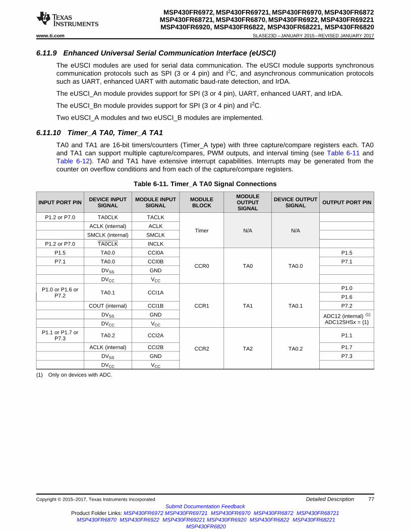
77
MSP430FR6972, MSP430FR69721, MSP430FR6970, MSP430FR6872MSP430FR68721, MSP430FR6870, MSP430FR6922, MSP430FR69221MSP430FR6920, MSP430FR6822, MSP430FR68221, MSP430FR6820
www.ti.com SLASE23D –JANUARY 2015–REVISED JANUARY 2017
Submit Documentation FeedbackProduct Folder Links: MSP430FR6972 MSP430FR69721 MSP430FR6970 MSP430FR6872 MSP430FR68721
MSP430FR6870 MSP430FR6922 MSP430FR69221 MSP430FR6920 MSP430FR6822 MSP430FR68221MSP430FR6820
Detailed DescriptionCopyright © 2015–2017, Texas Instruments Incorporated
(1) Only on devices with ADC.
6.11.9 Enhanced Universal Serial Communication Interface (eUSCI)The eUSCI modules are used for serial data communication. The eUSCI module supports synchronouscommunication protocols such as SPI (3 or 4 pin) and I2C, and asynchronous communication protocolssuch as UART, enhanced UART with automatic baud-rate detection, and IrDA.
The eUSCI_An module provides support for SPI (3 or 4 pin), UART, enhanced UART, and IrDA.
The eUSCI_Bn module provides support for SPI (3 or 4 pin) and I2C.
Two eUSCI_A modules and two eUSCI_B modules are implemented.
6.11.10 Timer_A TA0, Timer_A TA1TA0 and TA1 are 16-bit timers/counters (Timer_A type) with three capture/compare registers each. TA0and TA1 can support multiple capture/compares, PWM outputs, and interval timing (see Table 6-11 andTable 6-12). TA0 and TA1 have extensive interrupt capabilities. Interrupts may be generated from thecounter on overflow conditions and from each of the capture/compare registers.
Table 6-11. Timer_A TA0 Signal Connections
INPUT PORT PIN DEVICE INPUTSIGNAL
MODULE INPUTSIGNAL
MODULEBLOCK
MODULEOUTPUTSIGNAL
DEVICE OUTPUTSIGNAL OUTPUT PORT PIN
P1.2 or P7.0 TA0CLK TACLK
Timer N/A N/AACLK (internal) ACLK
SMCLK (internal) SMCLKP1.2 or P7.0 TA0CLK INCLK
P1.5 TA0.0 CCI0A
CCR0 TA0 TA0.0
P1.5P7.1 TA0.0 CCI0B P7.1
DVSS GNDDVCC VCC
P1.0 or P1.6 orP7.2 TA0.1 CCI1A
CCR1 TA1 TA0.1
P1.0P1.6
COUT (internal) CCI1B P7.2DVSS GND ADC12 (internal) (1)
ADC12SHSx = 1DVCC VCC
P1.1 or P1.7 orP7.3 TA0.2 CCI2A
CCR2 TA2 TA0.2
P1.1
ACLK (internal) CCI2B P1.7DVSS GND P7.3DVCC VCC

78
MSP430FR6972, MSP430FR69721, MSP430FR6970, MSP430FR6872MSP430FR68721, MSP430FR6870, MSP430FR6922, MSP430FR69221MSP430FR6920, MSP430FR6822, MSP430FR68221, MSP430FR6820SLASE23D –JANUARY 2015–REVISED JANUARY 2017 www.ti.com
Submit Documentation FeedbackProduct Folder Links: MSP430FR6972 MSP430FR69721 MSP430FR6970 MSP430FR6872 MSP430FR68721
MSP430FR6870 MSP430FR6922 MSP430FR69221 MSP430FR6920 MSP430FR6822 MSP430FR68221MSP430FR6820
Detailed Description Copyright © 2015–2017, Texas Instruments Incorporated
(1) Only on devices with ADC.
Table 6-12. Timer_A TA1 Signal Connections
INPUT PORT PIN DEVICE INPUTSIGNAL
MODULE INPUTSIGNAL
MODULEBLOCK
MODULEOUTPUTSIGNAL
DEVICE OUTPUTSIGNAL OUTPUT PORT PIN
P1.1 or P4.4 TA1CLK TACLK
Timer N/A N/AACLK (internal) ACLK
SMCLK (internal) SMCLKP1.1 or P4.4 TA1CLK INCLKP1.4 or P4.5 TA1.0 CCI0A
CCR0 TA0 TA1.0
P1.4DVSS CCI0B P4.5DVSS GNDDVCC VCC
P1.2 or P3.3 orP4.6 TA1.1 CCI1A
CCR1 TA1 TA1.1
P1.2P4.6
COUT (internal) CCI1B P3.3DVSS GND ADC12 (internal) (1)
ADC12SHSx = 4DVCC VCC
P1.3 or P4.7 TA1.2 CCI2A
CCR2 TA2 TA1.2
P1.3ACLK (internal) CCI2B P4.7
DVSS GNDDVCC VCC
(1) Only on devices with ADC.
6.11.11 Timer_A TA2TA2 is a 16-bit timer/counter (Timer_A type) with two capture/compare registers each and with internalconnections only. TA2 can support multiple capture/compares, PWM outputs, and interval timing (seeTable 6-13). TA2 has extensive interrupt capabilities. Interrupts may be generated from the counter onoverflow conditions and from each of the capture/compare registers.
Table 6-13. Timer_A TA2 Signal Connections
DEVICE INPUT SIGNAL MODULE INPUT NAME MODULE BLOCK MODULE OUTPUTSIGNAL DEVICE OUTPUT SIGNAL
COUT (internal) TACLK
Timer N/AACLK (internal) ACLK
SMCLK (internal) SMCLKFrom Capacitive Touch
I/O 0 (internal) INCLK
TA3 CCR0 output(internal) CCI0A
CCR0 TA0
TA3 CCI0A input
ACLK (internal) CCI0BDVSS GNDDVCC VCC
From Capacitive TouchI/O 0 (internal) CCI1A
CCR1 TA1
ADC12 (internal) (1)
ADC12SHSx = 5COUT (internal) CCI1B
DVSS GNDDVCC VCC

79
MSP430FR6972, MSP430FR69721, MSP430FR6970, MSP430FR6872MSP430FR68721, MSP430FR6870, MSP430FR6922, MSP430FR69221MSP430FR6920, MSP430FR6822, MSP430FR68221, MSP430FR6820
www.ti.com SLASE23D –JANUARY 2015–REVISED JANUARY 2017
Submit Documentation FeedbackProduct Folder Links: MSP430FR6972 MSP430FR69721 MSP430FR6970 MSP430FR6872 MSP430FR68721
MSP430FR6870 MSP430FR6922 MSP430FR69221 MSP430FR6920 MSP430FR6822 MSP430FR68221MSP430FR6820
Detailed DescriptionCopyright © 2015–2017, Texas Instruments Incorporated
(1) Only on devices with ADC.
6.11.12 Timer_A TA3TA3 is a 16-bit timer/counter (Timer_A type) with five capture/compare registers each and with internalconnections only. TA3 can support multiple capture/compares, PWM outputs, and interval timing (seeTable 6-14). TA3 has extensive interrupt capabilities. Interrupts may be generated from the counter onoverflow conditions and from each of the capture/compare registers.
Table 6-14. Timer_A TA3 Signal Connections
DEVICE INPUT SIGNAL MODULE INPUT NAME MODULE BLOCK MODULE OUTPUTSIGNAL DEVICE OUTPUT SIGNAL
COUT (internal) TACLK
Timer N/AACLK (internal) ACLK
SMCLK (internal) SMCLKFrom Capacitive Touch
I/O 1 (internal) INCLK
TA2 CCR0 output(internal) CCI0A
CCR0 TA0
TA2 CCI0A input
ACLK (internal) CCI0BDVSS GNDDVCC VCC
From Capacitive TouchI/O 1 (internal) CCI1A
CCR1 TA1
ADC12 (internal) (1)
ADC12SHSx = 6COUT (internal) CCI1B
DVSS GNDDVCC VCC
DVSS CCI2A
CCR2 TA2
P3.0DVSS (FR692x(1) and
FR682x(1) 64‑pinpackage)
CCI2BP3.0 (Note: Not available forFR692x(1) and FR682x(1)64-pin package devices)
DVSS GNDDVCC VCC
DVSS CCI3A
CCR3 TA3
P3.1DVSS (FR692x(1) and
FR682x(1) 64‑pinpackage)
CCI3BP3.1 (Note: Not available forFR692x(1) and FR682x(1)64-pin package devices)
DVSS GNDDVCC VCC
DVSS CCI4A
CCR4 TA4
P3.2DVSS (FR692x(1) and
FR682x(1) 64‑pinpackage)
CCI4BP3.2 (Note: Not available forFR692x(1) and FR682x(1)64-pin package devices)
DVSS GNDDVCC VCC

80
MSP430FR6972, MSP430FR69721, MSP430FR6970, MSP430FR6872MSP430FR68721, MSP430FR6870, MSP430FR6922, MSP430FR69221MSP430FR6920, MSP430FR6822, MSP430FR68221, MSP430FR6820SLASE23D –JANUARY 2015–REVISED JANUARY 2017 www.ti.com
Submit Documentation FeedbackProduct Folder Links: MSP430FR6972 MSP430FR69721 MSP430FR6970 MSP430FR6872 MSP430FR68721
MSP430FR6870 MSP430FR6922 MSP430FR69221 MSP430FR6920 MSP430FR6822 MSP430FR68221MSP430FR6820
Detailed Description Copyright © 2015–2017, Texas Instruments Incorporated
(1) Only on devices with ADC.
6.11.13 Timer_B TB0TB0 is a 16-bit timer/counter (Timer_B type) with seven capture/compare registers each. TB0 can supportmultiple capture/compares, PWM outputs, and interval timing (see Table 6-15). TB0 has extensiveinterrupt capabilities. Interrupts may be generated from the counter on overflow conditions and from eachof the capture/compare registers.
Table 6-15. Timer_B TB0 Signal Connections
INPUT PORT PIN DEVICE INPUTSIGNAL
MODULE INPUTSIGNAL
MODULEBLOCK
MODULEOUTPUTSIGNAL
DEVICE OUTPUTSIGNAL OUTPUT PORT PIN
P2.0 or P3.3 orP5.7 TB0CLK TBCLK
Timer N/A N/AACLK (internal) ACLK
SMCLK (internal) SMCLKP2.0 or P3.3 or
P5.7 TB0CLK INCLK
P3.4 TB0.0 CCI0A
CCR0 TB0 TB0.0
P3.4P6.4 TB0.0 CCI0B P6.4
DVSS GND ADC12 (internal) (1)
ADC12SHSx = 2DVCC VCC
P3.5 or P6.5 TB0.1 CCI1A
CCR1 TB1 TB0.1
P3.5COUT (internal) CCI1B P6.5
DVSS GND ADC12 (internal) (1)
ADC12SHSx = 3DVCC VCC
P3.6 or P6.6 TB0.2 CCI2A
CCR2 TB2 TB0.2
P3.6ACLK (internal) CCI2B P6.6
DVSS GNDDVCC VCC
DVSS CCI3A
CCR3 TB3 TB0.3P3.7 TB0.3 CCI3B P3.7
DVSS GNDDVCC VCC
DVSS CCI4A
CCR4 TB4 TB0.4P2.2 TB0.4 CCI4B P2.2
DVSS GNDDVCC VCC
DVSS CCI5A
CCR5 TB5 TB0.5P2.1 TB0.5 CCI5B P2.1
DVSS GNDDVCC VCC
DVSS CCI6A
CCR6 TB6 TB0.6P2.0 TB0.6 CCI6B P2.0
DVSS GNDDVCC VCC

81
MSP430FR6972, MSP430FR69721, MSP430FR6970, MSP430FR6872MSP430FR68721, MSP430FR6870, MSP430FR6922, MSP430FR69221MSP430FR6920, MSP430FR6822, MSP430FR68221, MSP430FR6820
www.ti.com SLASE23D –JANUARY 2015–REVISED JANUARY 2017
Submit Documentation FeedbackProduct Folder Links: MSP430FR6972 MSP430FR69721 MSP430FR6970 MSP430FR6872 MSP430FR68721
MSP430FR6870 MSP430FR6922 MSP430FR69221 MSP430FR6920 MSP430FR6822 MSP430FR68221MSP430FR6820
Detailed DescriptionCopyright © 2015–2017, Texas Instruments Incorporated
6.11.14 ADC12_BThe ADC12_B module supports fast 12-bit analog-to-digital conversions with differential and single-endedinputs. The module implements a 12-bit SAR core, sample select control, reference generator and aconversion result buffer. A window comparator with a lower and upper limits allows CPU-independentresult monitoring with three window comparator interrupt flags.
Table 6-16 summarizes the available external trigger sources.
Table 6-17 lists the available multiplexing between internal and external analog inputs.
Table 6-16. ADC12_B Trigger Signal Connections
ADC12SHSx CONNECTED TRIGGERSOURCEBINARY DECIMAL
000 0 Software (ADC12SC)001 1 Timer_A TA0 CCR1 output010 2 Timer_B TB0 CCR0 output011 3 Timer_B TB0 CCR1 output100 4 Timer_A TA1 CCR1 output101 5 Timer_A TA2 CCR1 output110 6 Timer_A TA3 CCR1 output111 7 Reserved (DVSS)
(1) N/A: No internal signal available on this device.
Table 6-17. ADC12_B External and Internal Signal Mapping
CONTROL BIT EXTERNAL(CONTROL BIT = 0)
INTERNAL(CONTROL BIT = 1)
ADC12BATMAP A31 Battery monitorADC12TCMAP A30 Temperature sensor
ADC12CH0MAP A29 N/A (1)
ADC12CH1MAP A28 N/A (1)
ADC12CH2MAP A27 N/A (1)
ADC12CH3MAP A26 N/A (1)
6.11.15 Comparator_EThe primary function of the Comparator_E module is to support precision slope analog-to-digitalconversions, battery voltage supervision, and monitoring of external analog signals.
6.11.16 CRC16The CRC16 module produces a signature based on a sequence of entered data values and can be usedfor data checking purposes. The CRC16 signature is based on the CRC-CCITT standard.
6.11.17 CRC32The CRC32 module produces a signature based on a sequence of entered data values and can be usedfor data checking purposes. The CRC32 signature is based on the ISO 3309 standard.
6.11.18 AES256 AcceleratorThe AES accelerator module performs encryption and decryption of 128-bit data with 128-, 192-, or 256-bit keys according to the advanced encryption standard (AES) (FIPS PUB 197) in hardware.
82
MSP430FR6972, MSP430FR69721, MSP430FR6970, MSP430FR6872MSP430FR68721, MSP430FR6870, MSP430FR6922, MSP430FR69221MSP430FR6920, MSP430FR6822, MSP430FR68221, MSP430FR6820SLASE23D –JANUARY 2015–REVISED JANUARY 2017 www.ti.com
Submit Documentation FeedbackProduct Folder Links: MSP430FR6972 MSP430FR69721 MSP430FR6970 MSP430FR6872 MSP430FR68721
MSP430FR6870 MSP430FR6922 MSP430FR69221 MSP430FR6920 MSP430FR6822 MSP430FR68221MSP430FR6820
Detailed Description Copyright © 2015–2017, Texas Instruments Incorporated
6.11.19 True Random SeedThe Device Descriptor Info (TLV) (see Section 6.12) contains a 128-bit true random seed that can be usedto implement a deterministic random-number generator.
6.11.20 Shared Reference (REF_A)The REF_A module is responsible for generation of all critical reference voltages that can be used by thevarious analog peripherals in the device.
6.11.21 LCD_CThe LCD_C driver generates the segment and common signals required to drive a liquid crystal display(LCD). The LCD_C controller has dedicated data memories to hold segment drive information. Commonand segment signals are generated as defined by the mode. Static, and 2-mux up to 4-mux LCDs aresupported. The module can provide an LCD voltage independent of the supply voltage with its integratedcharge pump. It is possible to control the level of the LCD voltage and thus contrast by software. Themodule also provides an automatic blinking capability for individual segments in static, 2-mux, 3-mux, and4-mux modes.
To reduce system noise the charge pump can be temporarily disabled. Table 6-18 lists the availableautomatic charge pump disable options.
Table 6-18. LCD Automatic Charge Pump Disable Bits (LCDCPDISx)
CONTROL BIT DESCRIPTION
LCDCPDIS0LCD charge pump disable during ADC12 conversion.0b = LCD charge pump not automatically disabled during conversion1b = LCD charge pump automatically disabled during conversion
LCDCPDIS1 to LCDCPDIS7 No functionality
6.11.22 Embedded Emulation
6.11.22.1 Embedded Emulation Module (EEM)
The EEM supports real-time in-system debugging. The S version of the EEM has the following features:• Three hardware triggers or breakpoints on memory access• One hardware trigger or breakpoint on CPU register write access• Up to four hardware triggers that can be combined to form complex triggers or breakpoints• One cycle counter• Clock control on module level
6.11.22.2 EnergyTrace++™ Technology
The devices implement circuitry to support EnergyTrace++ technology. The EnergyTrace++ technologylets you observe information about the internal states of the microcontroller. These states include the CPUProgram Counter (PC), the ON or OFF status of the peripherals and the system clocks (regardless of theclock source), and the low-power mode currently in use. These states can always be read by a debugtool, even when the microcontroller sleeps in LPMx.5 modes.
The activity of the following modules can be observed:• MPY is calculating.• WDT is counting.• RTC is counting.• ADC: a sequence, sample, or conversion is active.• REF: REFBG or REFGEN active and BG in static mode.

83
MSP430FR6972, MSP430FR69721, MSP430FR6970, MSP430FR6872MSP430FR68721, MSP430FR6870, MSP430FR6922, MSP430FR69221MSP430FR6920, MSP430FR6822, MSP430FR68221, MSP430FR6820
www.ti.com SLASE23D –JANUARY 2015–REVISED JANUARY 2017
Submit Documentation FeedbackProduct Folder Links: MSP430FR6972 MSP430FR69721 MSP430FR6970 MSP430FR6872 MSP430FR68721
MSP430FR6870 MSP430FR6922 MSP430FR69221 MSP430FR6920 MSP430FR6822 MSP430FR68221MSP430FR6820
Detailed DescriptionCopyright © 2015–2017, Texas Instruments Incorporated
• COMP is on.• AES is encrypting or decrypting.• eUSCI_A0 is transferring (receiving or transmitting) data.• eUSCI_A1 is transferring (receiving or transmitting) data.• eUSCI_B0 is transferring (receiving or transmitting) data.• eUSCI_B1 is transferring (receiving or transmitting) data.• TB0 is counting.• TA0 is counting.• TA1 is counting.• TA2 is counting.• TA3 is counting.• LCD timing generator is active.

Px.y/Mod1/Mod2/Mod3/Sz
PxSEL1.y
PxDIR.y
PxIN.y
To module 1(A)
To module 2(A)
To module 3(A)
From module 1
PxOUT.y
1
0DVSS
DVCC 1
Pad Logic
Direction0: Input1: Output
PxREN.y
0 1
0 0
1 0
1 1
PxSEL0.y
0 1
0 0
1 0
1 1
From module 2
From module 2(B)
From module 1(B)
From module 3(B)
From module 3
Sz
LCDSz
84
MSP430FR6972, MSP430FR69721, MSP430FR6970, MSP430FR6872MSP430FR68721, MSP430FR6870, MSP430FR6922, MSP430FR69221MSP430FR6920, MSP430FR6822, MSP430FR68221, MSP430FR6820SLASE23D –JANUARY 2015–REVISED JANUARY 2017 www.ti.com
Submit Documentation FeedbackProduct Folder Links: MSP430FR6972 MSP430FR69721 MSP430FR6970 MSP430FR6872 MSP430FR68721
MSP430FR6870 MSP430FR6922 MSP430FR69221 MSP430FR6920 MSP430FR6822 MSP430FR68221MSP430FR6820
Detailed Description Copyright © 2015–2017, Texas Instruments Incorporated
6.11.23 Input/Output Diagrams
6.11.23.1 Digital I/O Functionality Port P1 to P7 and P9
The port pins provide the following features:• Interrupt and wakeup from LPMx.5 capability for ports P1 to P4• Capacitive touch functionality (see Section 6.11.23.2)• Up to three digital module input and/or output functions• LCD segment functionality (not all pins, package dependent)
Figure 6-1 shows the features and the corresponding control logic (besides the Capacitive Touch logic).Figure 6-1 is applicable for all port pins P1.0 to P9.7, unless a dedicated diagram is available in thefollowing sections. The module functions provided per pin and whether the direction is controlled by themodule or by the port direction register for the selected secondary function are described in the followingpin function tables.
A. The direction is either controlled by connected module or by the corresponding PxDIR.y bit. See pin function tables.B. The inputs from several pins towards a module are ORed together.
NOTE: Functional representation only.
Figure 6-1. General Port Pin Diagram
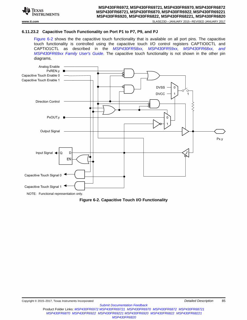
0
1
0
1
1
PxREN.y
PxOUT.y
Direction Control
Analog Enable
Capacitive Touch Enable 0
Output Signal
DVSS
DVCC
Input Signal
Px.y
Capacitive Touch Signal 0
Capacitive Touch Signal 1
EN
DQ
Capacitive Touch Enable 1
85
MSP430FR6972, MSP430FR69721, MSP430FR6970, MSP430FR6872MSP430FR68721, MSP430FR6870, MSP430FR6922, MSP430FR69221MSP430FR6920, MSP430FR6822, MSP430FR68221, MSP430FR6820
www.ti.com SLASE23D –JANUARY 2015–REVISED JANUARY 2017
Submit Documentation FeedbackProduct Folder Links: MSP430FR6972 MSP430FR69721 MSP430FR6970 MSP430FR6872 MSP430FR68721
MSP430FR6870 MSP430FR6922 MSP430FR69221 MSP430FR6920 MSP430FR6822 MSP430FR68221MSP430FR6820
Detailed DescriptionCopyright © 2015–2017, Texas Instruments Incorporated
6.11.23.2 Capacitive Touch Functionality on Port P1 to P7, P9, and PJ
Figure 6-2 shows the the capacitive touch functionality that is available on all port pins. The capacitivetouch functionality is controlled using the capacitive touch I/O control registers CAPTIO0CTL andCAPTIO1CTL as described in the MSP430FR58xx, MSP430FR59xx, MSP430FR68xx, andMSP430FR69xx Family User's Guide. The capacitive touch functionality is not shown in the other pindiagrams.
NOTE: Functional representation only.
Figure 6-2. Capacitive Touch I/O Functionality

P1.0/TA0.1/DMAE0/RTCCLK/A0/C0/VREF-/VeREF-
P1.1/TA0.2/TA1CLK/COUT/A1/C1/VREF+/VeREF+
P1.2/TA1.1/TA0CLK/COUT/A2/C2P1.3/TA1.2/A3/C3
P1SEL1.x
P1DIR.x
P1IN.x
DVSS
P1OUT.x
1
0DVSS
DVCC 1
To Comparator
From Comparator
Pad Logic
To ADC
From ADC
BusKeeper
Direction0: Input1: Output
CEPD.x
P1REN.x
0 1
0 0
1 0
1 1
P1SEL0.x
0 1
0 0
1 0
1 1
DVSS
DVSS
86
MSP430FR6972, MSP430FR69721, MSP430FR6970, MSP430FR6872MSP430FR68721, MSP430FR6870, MSP430FR6922, MSP430FR69221MSP430FR6920, MSP430FR6822, MSP430FR68221, MSP430FR6820SLASE23D –JANUARY 2015–REVISED JANUARY 2017 www.ti.com
Submit Documentation FeedbackProduct Folder Links: MSP430FR6972 MSP430FR69721 MSP430FR6970 MSP430FR6872 MSP430FR68721
MSP430FR6870 MSP430FR6922 MSP430FR69221 MSP430FR6920 MSP430FR6822 MSP430FR68221MSP430FR6820
Detailed Description Copyright © 2015–2017, Texas Instruments Incorporated
6.11.23.3 Port P1 (P1.0 to P1.3) Input/Output With Schmitt Trigger
Figure 6-3 shows the port diagram. Table 6-19 summarizes the selection of the pin functions.
NOTE: Functional representation only.
Figure 6-3. Port P1 (P1.0 to P1.3) Diagram
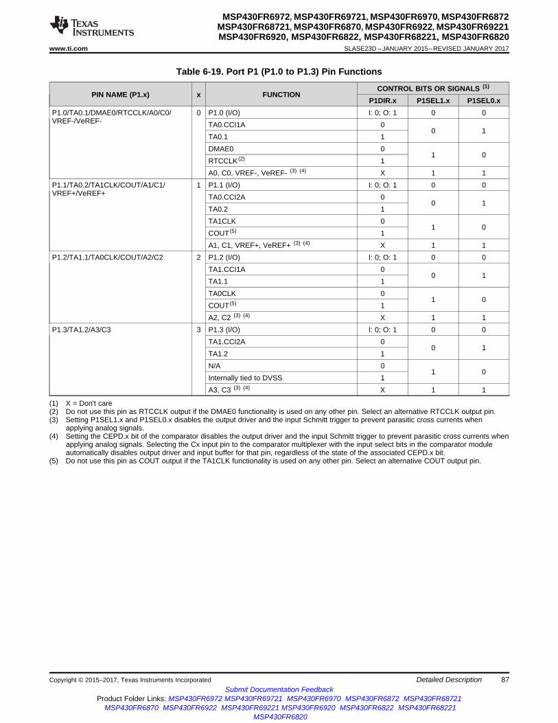
87
MSP430FR6972, MSP430FR69721, MSP430FR6970, MSP430FR6872MSP430FR68721, MSP430FR6870, MSP430FR6922, MSP430FR69221MSP430FR6920, MSP430FR6822, MSP430FR68221, MSP430FR6820
www.ti.com SLASE23D –JANUARY 2015–REVISED JANUARY 2017
Submit Documentation FeedbackProduct Folder Links: MSP430FR6972 MSP430FR69721 MSP430FR6970 MSP430FR6872 MSP430FR68721
MSP430FR6870 MSP430FR6922 MSP430FR69221 MSP430FR6920 MSP430FR6822 MSP430FR68221MSP430FR6820
Detailed DescriptionCopyright © 2015–2017, Texas Instruments Incorporated
(1) X = Don't care(2) Do not use this pin as RTCCLK output if the DMAE0 functionality is used on any other pin. Select an alternative RTCCLK output pin.(3) Setting P1SEL1.x and P1SEL0.x disables the output driver and the input Schmitt trigger to prevent parasitic cross currents when
applying analog signals.(4) Setting the CEPD.x bit of the comparator disables the output driver and the input Schmitt trigger to prevent parasitic cross currents when
applying analog signals. Selecting the Cx input pin to the comparator multiplexer with the input select bits in the comparator moduleautomatically disables output driver and input buffer for that pin, regardless of the state of the associated CEPD.x bit.
(5) Do not use this pin as COUT output if the TA1CLK functionality is used on any other pin. Select an alternative COUT output pin.
Table 6-19. Port P1 (P1.0 to P1.3) Pin Functions
PIN NAME (P1.x) x FUNCTIONCONTROL BITS OR SIGNALS (1)
P1DIR.x P1SEL1.x P1SEL0.xP1.0/TA0.1/DMAE0/RTCCLK/A0/C0/VREF-/VeREF-
0 P1.0 (I/O) I: 0; O: 1 0 0TA0.CCI1A 0
0 1TA0.1 1DMAE0 0
1 0RTCCLK (2) 1A0, C0, VREF-, VeREF- (3) (4) X 1 1
P1.1/TA0.2/TA1CLK/COUT/A1/C1/VREF+/VeREF+
1 P1.1 (I/O) I: 0; O: 1 0 0TA0.CCI2A 0
0 1TA0.2 1TA1CLK 0
1 0COUT (5) 1A1, C1, VREF+, VeREF+ (3) (4) X 1 1
P1.2/TA1.1/TA0CLK/COUT/A2/C2 2 P1.2 (I/O) I: 0; O: 1 0 0TA1.CCI1A 0
0 1TA1.1 1TA0CLK 0
1 0COUT (5) 1A2, C2 (3) (4) X 1 1
P1.3/TA1.2/A3/C3 3 P1.3 (I/O) I: 0; O: 1 0 0TA1.CCI2A 0
0 1TA1.2 1N/A 0
1 0Internally tied to DVSS 1A3, C3 (3) (4) X 1 1

88
MSP430FR6972, MSP430FR69721, MSP430FR6970, MSP430FR6872MSP430FR68721, MSP430FR6870, MSP430FR6922, MSP430FR69221MSP430FR6920, MSP430FR6822, MSP430FR68221, MSP430FR6820SLASE23D –JANUARY 2015–REVISED JANUARY 2017 www.ti.com
Submit Documentation FeedbackProduct Folder Links: MSP430FR6972 MSP430FR69721 MSP430FR6970 MSP430FR6872 MSP430FR68721
MSP430FR6870 MSP430FR6922 MSP430FR69221 MSP430FR6920 MSP430FR6822 MSP430FR68221MSP430FR6820
Detailed Description Copyright © 2015–2017, Texas Instruments Incorporated
(1) X = Don't care(2) Direction controlled by eUSCI_B0 module.(3) Direction controlled by eUSCI_A0 module.(4) Associated LCD segment is package dependent. See the pin diagrams and signal descriptions in Section 4.
6.11.23.4 Port P1 (P1.4 to P1.7) Input/Output With Schmitt Trigger
For the port diagram, see Figure 6-1. Table 6-20 summarizes the selection of the pin functions.
Table 6-20. Port P1 (P1.4 to P1.7) Pin Functions
PIN NAME (P1.x) x FUNCTIONCONTROL BITS OR SIGNALS (1)
P1DIR.x P1SEL1.x P1SEL0.x LCDSzP1.4/UCB0CLK/UCA0STE/TA1.0/Sz 4 P1.4 (I/O) I: 0; O: 1 0 0 0
UCB0CLK X (2) 0 1 0UCA0STE X (3) 1 0 0TA1.CCI0A 0
1 1 0TA1.0 1Sz (4) X X X 1
P1.5/UCB0STE/UCA0CLK/TA0.0/Sz 5 P1.5 (I/O) I: 0; O: 1 0 0 0UCB0STE X (2) 0 1 0UCA0CLK X (3) 1 0 0TA0.CCI0A 0
1 1 0TA0.0 1Sz (4) X X X 1
P1.6/UCB0SIMO/UCB0SDA/TA0.1/Sz
6 P1.6 (I/O) I: 0; O: 1 0 0 0UCB0SIMO/UCB0SDA X (2) 0 1 0N/A 0
1 0 0Internally tied to DVSS 1TA0.CCI1A 0
1 1 0TA0.1 1Sz (4) X X X 1
P1.7/UCB0SOMI/UCB0SCL/TA0.2/Sz
7 P1.7 (I/O) I: 0; O: 1 0 0 0UCB0SOMI/UCB0SCL X (2) 0 1 0N/A 0
1 0 0Internally tied to DVSS 1TA0.CCI2A 0
1 1 0TA0.2 1Sz (4) X X X 1

89
MSP430FR6972, MSP430FR69721, MSP430FR6970, MSP430FR6872MSP430FR68721, MSP430FR6870, MSP430FR6922, MSP430FR69221MSP430FR6920, MSP430FR6822, MSP430FR68221, MSP430FR6820
www.ti.com SLASE23D –JANUARY 2015–REVISED JANUARY 2017
Submit Documentation FeedbackProduct Folder Links: MSP430FR6972 MSP430FR69721 MSP430FR6970 MSP430FR6872 MSP430FR68721
MSP430FR6870 MSP430FR6922 MSP430FR69221 MSP430FR6920 MSP430FR6822 MSP430FR68221MSP430FR6820
Detailed DescriptionCopyright © 2015–2017, Texas Instruments Incorporated
(1) X = Don't care(2) Direction controlled by eUSCI_A0 module.(3) Associated LCD segment is package dependent. See the pin diagrams and signal descriptions in Section 4.
6.11.23.5 Port P2 (P2.0 to P2.3) Input/Output With Schmitt Trigger
For the port diagram, see Figure 6-1. Table 6-21 summarizes the selection of the pin functions.
Table 6-21. Port P2 (P2.0 to P2.3) Pin Functions
PIN NAME (P2.x) x FUNCTIONCONTROL BITS OR SIGNALS (1)
P2DIR.x P2SEL1.x P2SEL0.x LCDSzP2.0/UCA0SIMO/UCA0TXD/TB0.6/TB0CLK/Sz
0 P2.0 (I/O) I: 0; O: 1 0 0 0UCA0SIMO/UCA0TXD X (2) 0 1 0TB0.CCI6B 0
1 0 0TB0.6 1TB0CLK 0
1 1 0Internally tied to DVSS 1Sz (3) X X X 1
P2.1/UCA0SOMI/UCA0RXD/TB0.5/DMAE0/Sz
1 P2.1 (I/O) I: 0; O: 1 0 0 0UCA0SOMI/UCA0RXD X (2) 0 1 0TB0.CCI5B 0
1 0 0TB0.5 1DMA0E 0
1 1 0Internally tied to DVSS 1Sz (3) X X X 1
P2.2/UCA0CLK/TB0.4/RTCCLK/Sz 2 P2.2 (I/O) I: 0; O: 1 0 0 0UCA0CLK X (2) 0 1 0TB0.CCI4B 0
1 0 0TB0.4 1N/A 0
1 1 0RTCCLK 1Sz (3) X X X 1
P2.3/UCA0STE/TB0OUTH/Sz 3 P2.3 (I/O) I: 0; O: 1 0 0 0UCA0STE X (2) 0 1 0TB0OUTH 0
1 0 0Internally tied to DVSS 1N/A 0
1 1 0Internally tied to DVSS 1Sz (3) X X X 1

90
MSP430FR6972, MSP430FR69721, MSP430FR6970, MSP430FR6872MSP430FR68721, MSP430FR6870, MSP430FR6922, MSP430FR69221MSP430FR6920, MSP430FR6822, MSP430FR68221, MSP430FR6820SLASE23D –JANUARY 2015–REVISED JANUARY 2017 www.ti.com
Submit Documentation FeedbackProduct Folder Links: MSP430FR6972 MSP430FR69721 MSP430FR6970 MSP430FR6872 MSP430FR68721
MSP430FR6870 MSP430FR6922 MSP430FR69221 MSP430FR6920 MSP430FR6822 MSP430FR68221MSP430FR6820
Detailed Description Copyright © 2015–2017, Texas Instruments Incorporated
(1) X = Don't care(2) Direction controlled by eUSCI_B1 module.(3) Associated LCD segment is package dependent. See the pin diagrams and signal descriptions in Section 4.
6.11.23.6 Port P3 (P3.0 to P3.7) Input/Output With Schmitt Trigger
For the port diagram, see Figure 6-1. Table 6-22 and Table 6-23 summarize the selection of the pinfunctions.
Table 6-22. Port P3 (P3.0 to P3.3) Pin Functions
PIN NAME (P3.x) x FUNCTIONCONTROL BITS OR SIGNALS (1)
P3DIR.x P3SEL1.x P3SEL0.x LCDSzP3.0/UCB1CLK/Sz 0 P3.0 (I/O) I: 0; O: 1 0 0 0
UCB1CLK X (2) 0 1 0TA3.CCI2B (Note: not available forFR692x(1) and FR682x(1) 64-pinpackage devices)
0
1 0 0TA3.2Internally tied to DVSS (for FR692x(1)and FR682x(1) 64-pin package devices)
1
N/A 01 1 0
Internally tied to DVSS 1Sz (3) X X X 1
P3.1/UCB1SIMO/UCB1SDA/Sz 1 P3.1 (I/O) I: 0; O: 1 0 0 0UCB1SIMO/UCB1SDA X (2) 0 1 0TA3.CCI3B (Note: not available forFR692x(1) and FR682x(1) 64-pinpackage devices)
0
1 0 0TA3.3Internally tied to DVSS (for FR692x(1)and FR682x(1) 64-pin package devices)
1
N/A 01 1 0
Internally tied to DVSS 1Sz (3) X X X 1
P3.2/UCB1SOMI/UCB1SCL/Sz 2 P3.2 (I/O) I: 0; O: 1 0 0 0UCB1SOMI/UCB1SCL X (2) 0 1 0TA3.CCI4B (Note: not available forFR692x(1) and FR682x(1) 64-pinpackage devices)
0
1 0 0TA3.4Internally tied to DVSS (for FR692x(1)and FR682x(1) 64-pin package devices)
1
01 1 0
1Sz (3) X X X 1
P3.3/TA1.1/TB0CLK/Sz 3 P3.3 (I/O) I: 0; O: 1 0 0 0N/A 0
0 1 0Internally tied to DVSS 1TA1.CCI1A 0
1 0 0TA1.1 1TB0CLK 0
1 1 0Internally tied to DVSS 1Sz (3) X X X 1

91
MSP430FR6972, MSP430FR69721, MSP430FR6970, MSP430FR6872MSP430FR68721, MSP430FR6870, MSP430FR6922, MSP430FR69221MSP430FR6920, MSP430FR6822, MSP430FR68221, MSP430FR6820
www.ti.com SLASE23D –JANUARY 2015–REVISED JANUARY 2017
Submit Documentation FeedbackProduct Folder Links: MSP430FR6972 MSP430FR69721 MSP430FR6970 MSP430FR6872 MSP430FR68721
MSP430FR6870 MSP430FR6922 MSP430FR69221 MSP430FR6920 MSP430FR6822 MSP430FR68221MSP430FR6820
Detailed DescriptionCopyright © 2015–2017, Texas Instruments Incorporated
(1) X = Don't care(2) Direction controlled by eUSCI_A1 module.(3) Associated LCD segment is package dependent. See the pin diagrams and signal descriptions in Section 4.
Table 6-23. Port P3 (P3.4 to P3.7) Pin Functions
PIN NAME (P3.x) x FUNCTIONCONTROL BITS OR SIGNALS (1)
P3DIR.x P3SEL1.x P3SEL0.x LCDSzP3.4/UCA1SIMO/UCA1TXD/TB0.0/Sz
4 P3.4 (I/O) I: 0; O: 1 0 0 0UCA1SIMO/UCA1TXD X (2) 0 1 0TB0CCI0A 0
1 0 0TB0.0 1N/A 0
1 1 0Internally tied to DVSS 1Sz (3) X X X 1
P3.5/UCA1SOMI/UCA1RXD/TB0.1/Sz
5 P3.5 (I/O) I: 0; O: 1 0 0 0UCA1SOMI/UCA1RXD X (2) 0 1 0TB0CCI1A 0
1 0 0TB0.1 1N/A 0
1 1 0Internally tied to DVSS 1Sz (3) X X X 1
P3.6/UCA1CLK/TB0.2/Sz 6 P3.6 (I/O) I: 0; O: 1 0 0 0UCA1CLK X (2) 0 1 0TB0CCI2A 0
1 0 0TB0.2 1N/A 0
1 1 0Internally tied to DVSS 1Sz (3) X X X 1
P3.7/UCA1STE/TB0.3/Sz 7 P3.7 (I/O) I: 0; O: 1 0 0 0UCA1STE X (2) 0 1 0TB0CCI3B 0
1 0 0TB0.3 1N/A 0
1 1 0Internally tied to DVSS 1Sz (3) X X X 1

92
MSP430FR6972, MSP430FR69721, MSP430FR6970, MSP430FR6872MSP430FR68721, MSP430FR6870, MSP430FR6922, MSP430FR69221MSP430FR6920, MSP430FR6822, MSP430FR68221, MSP430FR6820SLASE23D –JANUARY 2015–REVISED JANUARY 2017 www.ti.com
Submit Documentation FeedbackProduct Folder Links: MSP430FR6972 MSP430FR69721 MSP430FR6970 MSP430FR6872 MSP430FR68721
MSP430FR6870 MSP430FR6922 MSP430FR69221 MSP430FR6920 MSP430FR6822 MSP430FR68221MSP430FR6820
Detailed Description Copyright © 2015–2017, Texas Instruments Incorporated
(1) X = Don't care(2) Direction controlled by eUSCI_A0 module.(3) Direction controlled by eUSCI_B1 module.(4) Associated LCD segment is package dependent. See the pin diagrams and signal descriptions in Section 4.
6.11.23.7 Port P4 (P4.2 to P4.7) Input/Output With Schmitt Trigger
For the port diagram, see Figure 6-1. Table 6-24 and Table 6-25 summarize the selection of the pinfunctions.
Table 6-24. Port P4 (P4.2 and P4.3) Pin Functions
PIN NAME (P4.x) x FUNCTIONCONTROL BITS OR SIGNALS (1)
P4DIR.x P4SEL1.x P4SEL0.x LCDSzP4.2/UCA0SIMO/UCA0TXD/UCB1CLK/Sz
2 P4.2 (I/O) I: 0; O: 1 0 0 0UCA0SIMO/UCA0TXD X (2) 0 1 0UCB1CLK X (3) 1 0 0N/A 0
1 1 0Internally tied to DVSS 1Sz (4) X X X 1
P4.3/UCA0SOMI/UCA0RXD/UCB1STE/Sz
3 P4.3 (I/O) I: 0; O: 1 0 0 0UCA0SOMI/UCA0RXD X (2) 0 1 0UCB1STE X (3) 1 0 0N/A 0
1 1 0Internally tied to DVSS 1Sz (4) X X X 1
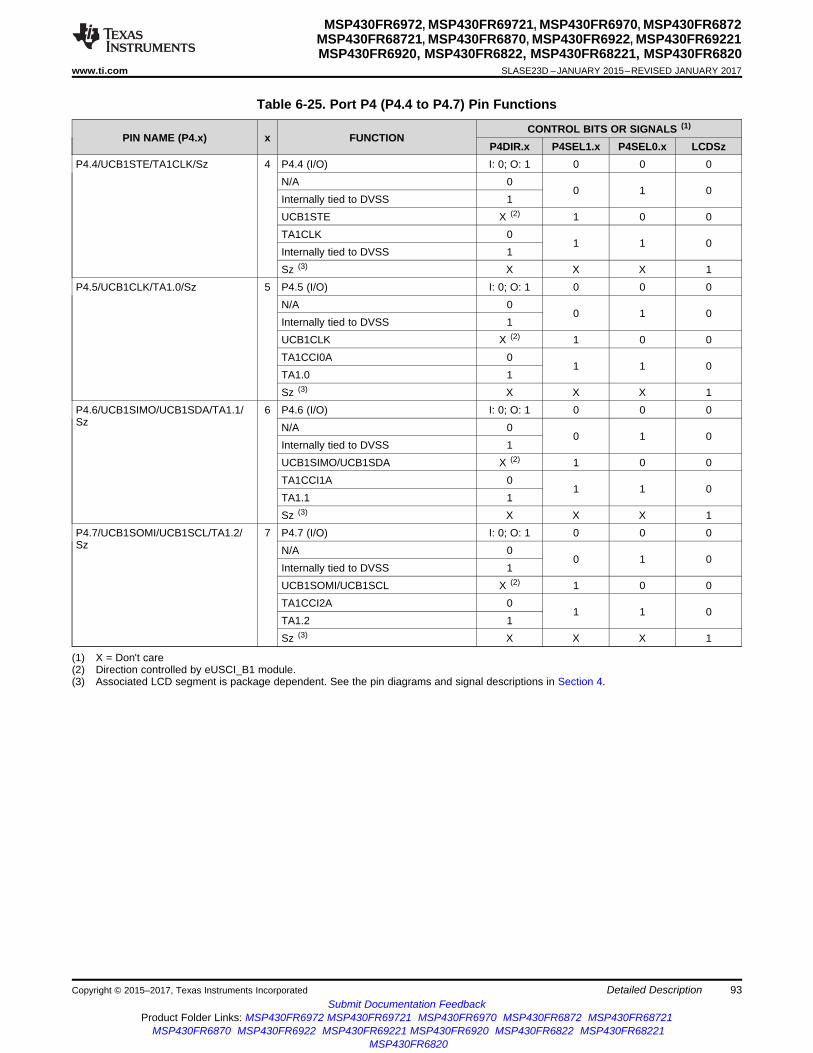
93
MSP430FR6972, MSP430FR69721, MSP430FR6970, MSP430FR6872MSP430FR68721, MSP430FR6870, MSP430FR6922, MSP430FR69221MSP430FR6920, MSP430FR6822, MSP430FR68221, MSP430FR6820
www.ti.com SLASE23D –JANUARY 2015–REVISED JANUARY 2017
Submit Documentation FeedbackProduct Folder Links: MSP430FR6972 MSP430FR69721 MSP430FR6970 MSP430FR6872 MSP430FR68721
MSP430FR6870 MSP430FR6922 MSP430FR69221 MSP430FR6920 MSP430FR6822 MSP430FR68221MSP430FR6820
Detailed DescriptionCopyright © 2015–2017, Texas Instruments Incorporated
(1) X = Don't care(2) Direction controlled by eUSCI_B1 module.(3) Associated LCD segment is package dependent. See the pin diagrams and signal descriptions in Section 4.
Table 6-25. Port P4 (P4.4 to P4.7) Pin Functions
PIN NAME (P4.x) x FUNCTIONCONTROL BITS OR SIGNALS (1)
P4DIR.x P4SEL1.x P4SEL0.x LCDSzP4.4/UCB1STE/TA1CLK/Sz 4 P4.4 (I/O) I: 0; O: 1 0 0 0
N/A 00 1 0
Internally tied to DVSS 1UCB1STE X (2) 1 0 0TA1CLK 0
1 1 0Internally tied to DVSS 1Sz (3) X X X 1
P4.5/UCB1CLK/TA1.0/Sz 5 P4.5 (I/O) I: 0; O: 1 0 0 0N/A 0
0 1 0Internally tied to DVSS 1UCB1CLK X (2) 1 0 0TA1CCI0A 0
1 1 0TA1.0 1Sz (3) X X X 1
P4.6/UCB1SIMO/UCB1SDA/TA1.1/Sz
6 P4.6 (I/O) I: 0; O: 1 0 0 0N/A 0
0 1 0Internally tied to DVSS 1UCB1SIMO/UCB1SDA X (2) 1 0 0TA1CCI1A 0
1 1 0TA1.1 1Sz (3) X X X 1
P4.7/UCB1SOMI/UCB1SCL/TA1.2/Sz
7 P4.7 (I/O) I: 0; O: 1 0 0 0N/A 0
0 1 0Internally tied to DVSS 1UCB1SOMI/UCB1SCL X (2) 1 0 0TA1CCI2A 0
1 1 0TA1.2 1Sz (3) X X X 1
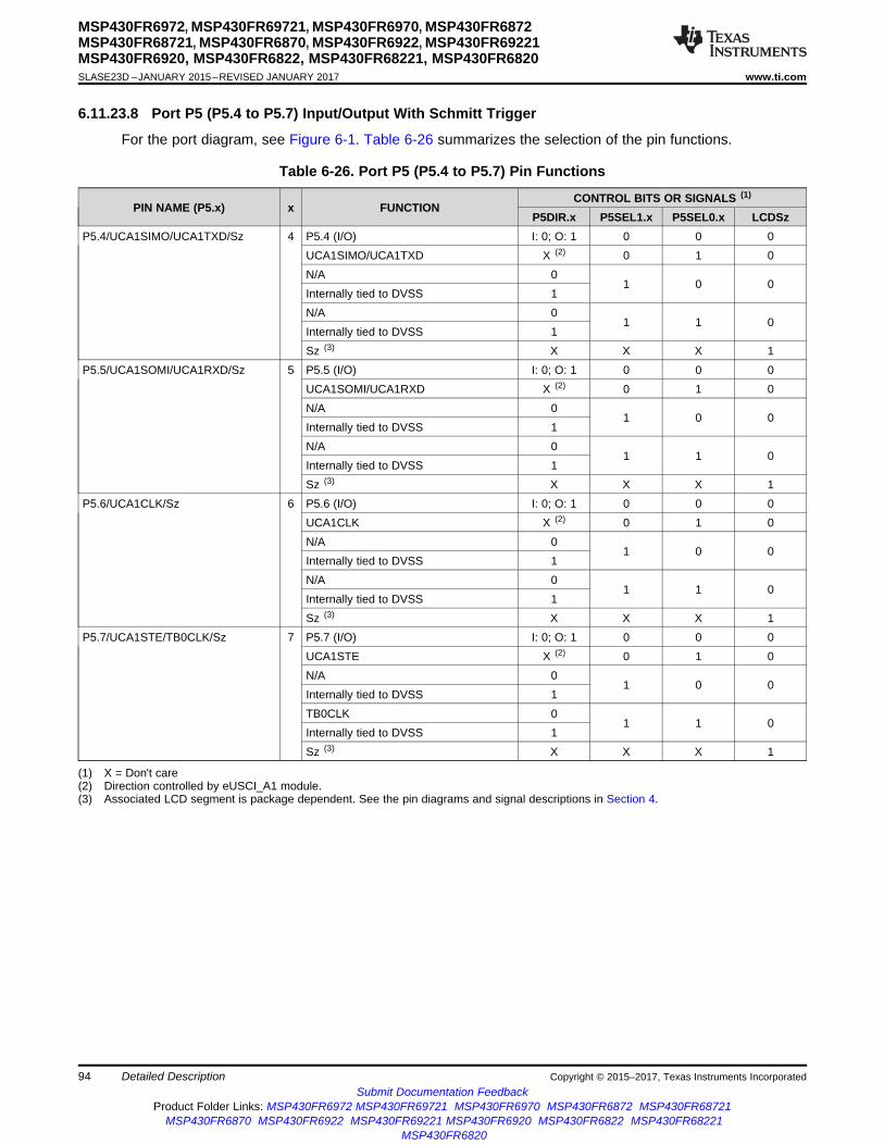
94
MSP430FR6972, MSP430FR69721, MSP430FR6970, MSP430FR6872MSP430FR68721, MSP430FR6870, MSP430FR6922, MSP430FR69221MSP430FR6920, MSP430FR6822, MSP430FR68221, MSP430FR6820SLASE23D –JANUARY 2015–REVISED JANUARY 2017 www.ti.com
Submit Documentation FeedbackProduct Folder Links: MSP430FR6972 MSP430FR69721 MSP430FR6970 MSP430FR6872 MSP430FR68721
MSP430FR6870 MSP430FR6922 MSP430FR69221 MSP430FR6920 MSP430FR6822 MSP430FR68221MSP430FR6820
Detailed Description Copyright © 2015–2017, Texas Instruments Incorporated
(1) X = Don't care(2) Direction controlled by eUSCI_A1 module.(3) Associated LCD segment is package dependent. See the pin diagrams and signal descriptions in Section 4.
6.11.23.8 Port P5 (P5.4 to P5.7) Input/Output With Schmitt Trigger
For the port diagram, see Figure 6-1. Table 6-26 summarizes the selection of the pin functions.
Table 6-26. Port P5 (P5.4 to P5.7) Pin Functions
PIN NAME (P5.x) x FUNCTIONCONTROL BITS OR SIGNALS (1)
P5DIR.x P5SEL1.x P5SEL0.x LCDSzP5.4/UCA1SIMO/UCA1TXD/Sz 4 P5.4 (I/O) I: 0; O: 1 0 0 0
UCA1SIMO/UCA1TXD X (2) 0 1 0N/A 0
1 0 0Internally tied to DVSS 1N/A 0
1 1 0Internally tied to DVSS 1Sz (3) X X X 1
P5.5/UCA1SOMI/UCA1RXD/Sz 5 P5.5 (I/O) I: 0; O: 1 0 0 0UCA1SOMI/UCA1RXD X (2) 0 1 0N/A 0
1 0 0Internally tied to DVSS 1N/A 0
1 1 0Internally tied to DVSS 1Sz (3) X X X 1
P5.6/UCA1CLK/Sz 6 P5.6 (I/O) I: 0; O: 1 0 0 0UCA1CLK X (2) 0 1 0N/A 0
1 0 0Internally tied to DVSS 1N/A 0
1 1 0Internally tied to DVSS 1Sz (3) X X X 1
P5.7/UCA1STE/TB0CLK/Sz 7 P5.7 (I/O) I: 0; O: 1 0 0 0UCA1STE X (2) 0 1 0N/A 0
1 0 0Internally tied to DVSS 1TB0CLK 0
1 1 0Internally tied to DVSS 1Sz (3) X X X 1

P6.0/R23P6.1/R13/LCDREFP6.2/COUT/R03P6.3/COM0P6.4/TB0.0/COM1P6.5/TB0.1/COM2P6.6/TB0.2/COM3
P6SEL1.x
P6DIR.x
P6IN.x
From module 1
P6OUT.x
1
0DVSS
DVCC 1
To/FromLCD module
Pad Logic
BusKeeper
Direction0: Input1: Output
P6REN.x
0 1
0 0
1 0
1 1
P6SEL0.x
0 1
0 0
1 0
1 1
From module 2
DVSS
To module 1(A)
To module 2(A)
95
MSP430FR6972, MSP430FR69721, MSP430FR6970, MSP430FR6872MSP430FR68721, MSP430FR6870, MSP430FR6922, MSP430FR69221MSP430FR6920, MSP430FR6822, MSP430FR68221, MSP430FR6820
www.ti.com SLASE23D –JANUARY 2015–REVISED JANUARY 2017
Submit Documentation FeedbackProduct Folder Links: MSP430FR6972 MSP430FR69721 MSP430FR6970 MSP430FR6872 MSP430FR68721
MSP430FR6870 MSP430FR6922 MSP430FR69221 MSP430FR6920 MSP430FR6822 MSP430FR68221MSP430FR6820
Detailed DescriptionCopyright © 2015–2017, Texas Instruments Incorporated
6.11.23.9 Port P6 (P6.0 to P6.6) Input/Output With Schmitt Trigger
Figure 6-4 shows the port diagram. Table 6-27 and Table 6-28 summarize the selection of the pinfunctions.
NOTE: Functional representation only.
Figure 6-4. Port P6 (P6.0 to P6.6) Diagram

96
MSP430FR6972, MSP430FR69721, MSP430FR6970, MSP430FR6872MSP430FR68721, MSP430FR6870, MSP430FR6922, MSP430FR69221MSP430FR6920, MSP430FR6822, MSP430FR68221, MSP430FR6820SLASE23D –JANUARY 2015–REVISED JANUARY 2017 www.ti.com
Submit Documentation FeedbackProduct Folder Links: MSP430FR6972 MSP430FR69721 MSP430FR6970 MSP430FR6872 MSP430FR68721
MSP430FR6870 MSP430FR6922 MSP430FR69221 MSP430FR6920 MSP430FR6822 MSP430FR68221MSP430FR6820
Detailed Description Copyright © 2015–2017, Texas Instruments Incorporated
(1) X = Don't care(2) Setting P6SEL1.x and P6SEL0.x disables the output driver and the input Schmitt trigger to prevent parasitic cross currents when
applying analog signals.
Table 6-27. Port P6 (P6.0 to P6.2) Pin Functions
PIN NAME (P6.x) x FUNCTIONCONTROL BITS OR SIGNALS (1)
P6DIR.x P6SEL1.x P6SEL0.xP6.0/R23 0 P6.0 (I/O) I: 0; O: 1 0 0
N/A 00 1
Internally tied to DVSS 1N/A 0
1 0Internally tied to DVSS 1R23 (2) X 1 1
P6.1/R13/LCDREF 1 P6.1 (I/O) I: 0; O: 1 0 0N/A 0
0 1Internally tied to DVSS 1N/A 0
1 0Internally tied to DVSS 1R13/LCDREF (2) X 1 1
P6.2/COUT/R03 2 P6.2 (I/O) I: 0; O: 1 0 0N/A 0
0 1COUT 1N/A 0
1 0Internally tied to DVSS 1R03 (2) X 1 1
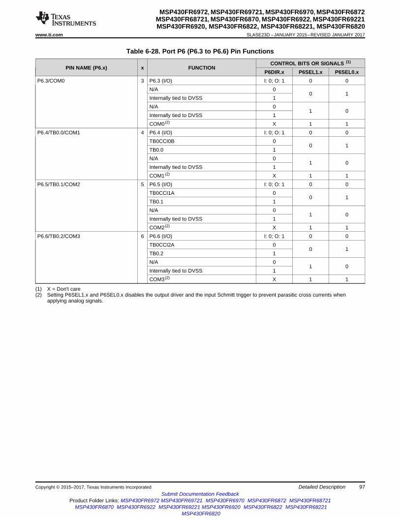
97
MSP430FR6972, MSP430FR69721, MSP430FR6970, MSP430FR6872MSP430FR68721, MSP430FR6870, MSP430FR6922, MSP430FR69221MSP430FR6920, MSP430FR6822, MSP430FR68221, MSP430FR6820
www.ti.com SLASE23D –JANUARY 2015–REVISED JANUARY 2017
Submit Documentation FeedbackProduct Folder Links: MSP430FR6972 MSP430FR69721 MSP430FR6970 MSP430FR6872 MSP430FR68721
MSP430FR6870 MSP430FR6922 MSP430FR69221 MSP430FR6920 MSP430FR6822 MSP430FR68221MSP430FR6820
Detailed DescriptionCopyright © 2015–2017, Texas Instruments Incorporated
(1) X = Don't care(2) Setting P6SEL1.x and P6SEL0.x disables the output driver and the input Schmitt trigger to prevent parasitic cross currents when
applying analog signals.
Table 6-28. Port P6 (P6.3 to P6.6) Pin Functions
PIN NAME (P6.x) x FUNCTIONCONTROL BITS OR SIGNALS (1)
P6DIR.x P6SEL1.x P6SEL0.xP6.3/COM0 3 P6.3 (I/O) I: 0; O: 1 0 0
N/A 00 1
Internally tied to DVSS 1N/A 0
1 0Internally tied to DVSS 1COM0 (2) X 1 1
P6.4/TB0.0/COM1 4 P6.4 (I/O) I: 0; O: 1 0 0TB0CCI0B 0
0 1TB0.0 1N/A 0
1 0Internally tied to DVSS 1COM1 (2) X 1 1
P6.5/TB0.1/COM2 5 P6.5 (I/O) I: 0; O: 1 0 0TB0CCI1A 0
0 1TB0.1 1N/A 0
1 0Internally tied to DVSS 1COM2 (2) X 1 1
P6.6/TB0.2/COM3 6 P6.6 (I/O) I: 0; O: 1 0 0TB0CCI2A 0
0 1TB0.2 1N/A 0
1 0Internally tied to DVSS 1COM3 (2) X 1 1

98
MSP430FR6972, MSP430FR69721, MSP430FR6970, MSP430FR6872MSP430FR68721, MSP430FR6870, MSP430FR6922, MSP430FR69221MSP430FR6920, MSP430FR6822, MSP430FR68221, MSP430FR6820SLASE23D –JANUARY 2015–REVISED JANUARY 2017 www.ti.com
Submit Documentation FeedbackProduct Folder Links: MSP430FR6972 MSP430FR69721 MSP430FR6970 MSP430FR6872 MSP430FR68721
MSP430FR6870 MSP430FR6922 MSP430FR69221 MSP430FR6920 MSP430FR6822 MSP430FR68221MSP430FR6820
Detailed Description Copyright © 2015–2017, Texas Instruments Incorporated
(1) X = Don't care(2) Associated LCD segment is package dependent. See the pin diagrams and signal descriptions in Section 4.
6.11.23.10 Port P7 (P7.0 to P7.4) Input/Output With Schmitt Trigger
For the port diagram, see Figure 6-1. Table 6-29 and Table 6-30 summarize the selection of the pinfunctions.
Table 6-29. Port P7 (P7.0 to P7.3) Pin Functions
PIN NAME (P7.x) x FUNCTIONCONTROL BITS OR SIGNALS (1)
P7DIR.x P7SEL1.x P7SEL0.x LCDSzP7.0/TA0CLK/Sz 0 P7.0 (I/O) I: 0; O: 1 0 0 0
TA0CLK 00 1 0
Internally tied to DVSS 1N/A 0
1 0 0Internally tied to DVSS 1N/A 0
1 1 0Internally tied to DVSS 1Sz (2) X X X 1
P7.1/TA0.0/ACLK/Sz 1 P7.1 (I/O) I: 0; O: 1 0 0 0TA0CCI0B 0
0 1 0TA0.0 1N/A 0
1 0 0Internally tied to DVSS 1N/A 0
1 1 0ACLK 1Sz (2) X X X 1
P7.2/TA0.1/Sz 2 P7.2 (I/O) I: 0; O: 1 0 0 0TA0CCI1A 0
0 1 0TA0.1 1N/A 0
1 0 0Internally tied to DVSS 1N/A 0
1 1 0N/A 1Sz (2) X X X 1
P7.3/TA0.2/Sz 3 P7.3 (I/O) I: 0; O: 1 0 0 0TA0CCI2A 0
0 1 0TA0.2 1N/A 0
1 0 0Internally tied to DVSS 1N/A 0
1 1 0Internally tied to DVSS 1Sz (2) X X X 1
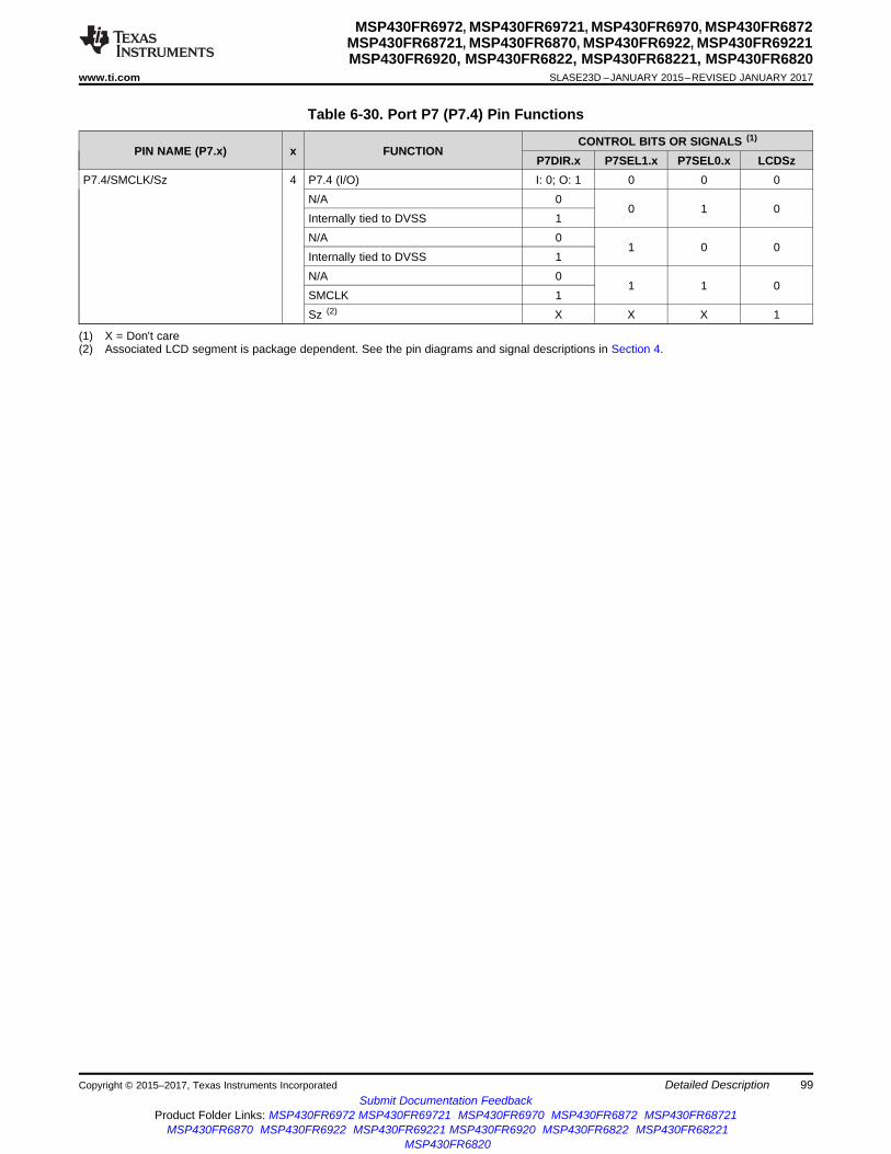
99
MSP430FR6972, MSP430FR69721, MSP430FR6970, MSP430FR6872MSP430FR68721, MSP430FR6870, MSP430FR6922, MSP430FR69221MSP430FR6920, MSP430FR6822, MSP430FR68221, MSP430FR6820
www.ti.com SLASE23D –JANUARY 2015–REVISED JANUARY 2017
Submit Documentation FeedbackProduct Folder Links: MSP430FR6972 MSP430FR69721 MSP430FR6970 MSP430FR6872 MSP430FR68721
MSP430FR6870 MSP430FR6922 MSP430FR69221 MSP430FR6920 MSP430FR6822 MSP430FR68221MSP430FR6820
Detailed DescriptionCopyright © 2015–2017, Texas Instruments Incorporated
(1) X = Don't care(2) Associated LCD segment is package dependent. See the pin diagrams and signal descriptions in Section 4.
Table 6-30. Port P7 (P7.4) Pin Functions
PIN NAME (P7.x) x FUNCTIONCONTROL BITS OR SIGNALS (1)
P7DIR.x P7SEL1.x P7SEL0.x LCDSzP7.4/SMCLK/Sz 4 P7.4 (I/O) I: 0; O: 1 0 0 0
N/A 00 1 0
Internally tied to DVSS 1N/A 0
1 0 0Internally tied to DVSS 1N/A 0
1 1 0SMCLK 1Sz (2) X X X 1

P9.4/A12/C12P9.5/A13/C13P9.6/A14/C14P9.7/A15/C15P9SEL1.x
P9DIR.x
P9IN.x
DVSS
P9OUT.x
1
0DVSS
DVCC 1
To Comparator
From Comparator
Pad Logic
To ADC
From ADC
BusKeeper
Direction0: Input1: Output
CEPD.x
P9REN.x
0 1
0 0
1 0
1 1
P9SEL0.x
0 1
0 0
1 0
1 1
DVSS
DVSS
100
MSP430FR6972, MSP430FR69721, MSP430FR6970, MSP430FR6872MSP430FR68721, MSP430FR6870, MSP430FR6922, MSP430FR69221MSP430FR6920, MSP430FR6822, MSP430FR68221, MSP430FR6820SLASE23D –JANUARY 2015–REVISED JANUARY 2017 www.ti.com
Submit Documentation FeedbackProduct Folder Links: MSP430FR6972 MSP430FR69721 MSP430FR6970 MSP430FR6872 MSP430FR68721
MSP430FR6870 MSP430FR6922 MSP430FR69221 MSP430FR6920 MSP430FR6822 MSP430FR68221MSP430FR6820
Detailed Description Copyright © 2015–2017, Texas Instruments Incorporated
6.11.23.11 Port P9 (P9.4 to P9.7) Input/Output With Schmitt Trigger
Figure 6-5 shows the port diagram. Table 6-31 summarizes the selection of the pin functions.
NOTE: Functional representation only.
Figure 6-5. Port P9 (P9.4 to P9.7) Diagram

101
MSP430FR6972, MSP430FR69721, MSP430FR6970, MSP430FR6872MSP430FR68721, MSP430FR6870, MSP430FR6922, MSP430FR69221MSP430FR6920, MSP430FR6822, MSP430FR68221, MSP430FR6820
www.ti.com SLASE23D –JANUARY 2015–REVISED JANUARY 2017
Submit Documentation FeedbackProduct Folder Links: MSP430FR6972 MSP430FR69721 MSP430FR6970 MSP430FR6872 MSP430FR68721
MSP430FR6870 MSP430FR6922 MSP430FR69221 MSP430FR6920 MSP430FR6822 MSP430FR68221MSP430FR6820
Detailed DescriptionCopyright © 2015–2017, Texas Instruments Incorporated
(1) X = Don't care(2) Setting P9SEL1.x and P9SEL0.x disables the output driver and the input Schmitt trigger to prevent parasitic cross currents when
applying analog signals.(3) Setting the CEPD.x bit of the comparator disables the output driver and the input Schmitt trigger to prevent parasitic cross currents when
applying analog signals. Selecting the Cx input pin to the comparator multiplexer with the input select bits in the comparator moduleautomatically disables output driver and input buffer for that pin, regardless of the state of the associated CEPD.x bit.
Table 6-31. Port P9 (P9.4 to P9.7) Pin Functions
PIN NAME (P9.x) x FUNCTIONCONTROL BITS OR SIGNALS (1)
P9DIR.x P9SEL1.x P9SEL0.xP9.4/A12/C12 4 P9.4 (I/O) I: 0; O: 1 0 0
N/A 00 1
Internally tied to DVSS 1N/A 0
1 0Internally tied to DVSS 1A12/C12 (2) (3) X 1 1
P9.5/A13/C13 5 P9.5 (I/O) I: 0; O: 1 0 0N/A 0
0 1Internally tied to DVSS 1N/A 0
1 0Internally tied to DVSS 1A13/C13 (2) (3) X 1 1
P9.6/A14/C14 6 P9.6 (I/O) I: 0; O: 1 0 0N/A 0
0 1Internally tied to DVSS 1N/A 0
1 0Internally tied to DVSS 1A14/C14 (2) (3) X 1 1
P9.7/A15/C15 7 P9.7 (I/O) I: 0; O: 1 0 0N/A 0
0 1Internally tied to DVSS 1N/A 0
1 0Internally tied to DVSS 1A15/C15 (2) (3) X 1 1

PJ.4/LFXIN
PJSEL1.4
PJDIR.4
PJIN.4
EN
To modules
DVSS
PJOUT.4
1
0DVSS
DVCC 1
D
To LFXT XIN
Pad Logic
BusKeeper
Direction0: Input1: Output
PJREN.4
0 1
0 0
1 0
1 1
PJSEL0.4
0 1
0 0
1 0
1 1
DVSS
DVSS
102
MSP430FR6972, MSP430FR69721, MSP430FR6970, MSP430FR6872MSP430FR68721, MSP430FR6870, MSP430FR6922, MSP430FR69221MSP430FR6920, MSP430FR6822, MSP430FR68221, MSP430FR6820SLASE23D –JANUARY 2015–REVISED JANUARY 2017 www.ti.com
Submit Documentation FeedbackProduct Folder Links: MSP430FR6972 MSP430FR69721 MSP430FR6970 MSP430FR6872 MSP430FR68721
MSP430FR6870 MSP430FR6922 MSP430FR69221 MSP430FR6920 MSP430FR6822 MSP430FR68221MSP430FR6820
Detailed Description Copyright © 2015–2017, Texas Instruments Incorporated
6.11.23.12 Port PJ (PJ.4 and PJ.5) Input/Output With Schmitt Trigger
Figure 6-6 and Figure 6-7 show the port diagrams. Table 6-32 summarizes the selection of the pinfunctions.
NOTE: Functional representation only.
Figure 6-6. Port PJ (PJ.4) Diagram

PJ.5/LFXOUT
PJSEL1.5
PJDIR.5
PJIN.5
EN
To modules
DVSS
PJOUT.5
1
0DVSS
DVCC 1
D
To LFXT XOUT
Pad Logic
BusKeeper
Direction0: Input1: Output
PJREN.5
0 1
0 0
1 0
1 1
PJSEL0.5
0 1
0 0
1 0
1 1
DVSS
DVSS
PJSEL1.4
PJSEL0.4
LFXTBYPASS
103
MSP430FR6972, MSP430FR69721, MSP430FR6970, MSP430FR6872MSP430FR68721, MSP430FR6870, MSP430FR6922, MSP430FR69221MSP430FR6920, MSP430FR6822, MSP430FR68221, MSP430FR6820
www.ti.com SLASE23D –JANUARY 2015–REVISED JANUARY 2017
Submit Documentation FeedbackProduct Folder Links: MSP430FR6972 MSP430FR69721 MSP430FR6970 MSP430FR6872 MSP430FR68721
MSP430FR6870 MSP430FR6922 MSP430FR69221 MSP430FR6920 MSP430FR6822 MSP430FR68221MSP430FR6820
Detailed DescriptionCopyright © 2015–2017, Texas Instruments Incorporated
NOTE: Functional representation only.
Figure 6-7. Port PJ (PJ.5) Diagram

104
MSP430FR6972, MSP430FR69721, MSP430FR6970, MSP430FR6872MSP430FR68721, MSP430FR6870, MSP430FR6922, MSP430FR69221MSP430FR6920, MSP430FR6822, MSP430FR68221, MSP430FR6820SLASE23D –JANUARY 2015–REVISED JANUARY 2017 www.ti.com
Submit Documentation FeedbackProduct Folder Links: MSP430FR6972 MSP430FR69721 MSP430FR6970 MSP430FR6872 MSP430FR68721
MSP430FR6870 MSP430FR6922 MSP430FR69221 MSP430FR6920 MSP430FR6822 MSP430FR68221MSP430FR6820
Detailed Description Copyright © 2015–2017, Texas Instruments Incorporated
(1) X = Don't care(2) Setting PJSEL1.4 = 0 and PJSEL0.4 = 1 causes the general-purpose I/O to be disabled. When LFXTBYPASS = 0, PJ.4 and PJ.5 are
configured for crystal operation and PJSEL1.5 and PJSEL0.5 are don't care. When LFXTBYPASS = 1, PJ.4 is configured for bypassoperation and PJ.5 is configured as general-purpose I/O.
(3) When PJ.4 is configured in bypass mode, PJ.5 is configured as general-purpose I/O.(4) With PJSEL0.5 = 1 or PJSEL1.5 =1 the general-purpose I/O functionality is disabled. No input function is available. Configured as
output, the pin is actively pulled to zero.
Table 6-32. Port PJ (PJ.4 and PJ.5) Pin Functions
PIN NAME (PJ.x) x FUNCTIONCONTROL BITS OR SIGNALS (1)
PJDIR.x PJSEL1.5 PJSEL0.5 PJSEL1.4 PJSEL0.4 LFXTBYPASSPJ.4/LFXIN 4 PJ.4 (I/O) I: 0; O: 1 X X 0 0 X
N/A 0X X 1 X X
Internally tied to DVSS 1LFXIN crystal mode (2) X X X 0 1 0LFXIN bypass mode (2) X X X 0 1 1
PJ.5/LFXOUT 5PJ.5 (I/O) I: 0; O: 1 0 0
0 00
1 XX X 1 (3)
N/A 0 See (4) See (4)
0 00
1 XX X 1 (3)
Internally tied to DVSS 1 See (4) See (4)
0 00
1 XX X 1 (3)
LFXOUT crystal mode(2) X X X 0 1 0

PJ.6/HFXIN
PJSEL1.6
PJDIR.6
PJIN.6
EN
To modules
DVSS
PJOUT.6
1
0DVSS
DVCC 1
D
To HFXT XIN
Pad Logic
BusKeeper
Direction0: Input1: Output
PJREN.6
0 1
0 0
1 0
1 1
PJSEL0.6
0 1
0 0
1 0
1 1
DVSS
DVSS
105
MSP430FR6972, MSP430FR69721, MSP430FR6970, MSP430FR6872MSP430FR68721, MSP430FR6870, MSP430FR6922, MSP430FR69221MSP430FR6920, MSP430FR6822, MSP430FR68221, MSP430FR6820
www.ti.com SLASE23D –JANUARY 2015–REVISED JANUARY 2017
Submit Documentation FeedbackProduct Folder Links: MSP430FR6972 MSP430FR69721 MSP430FR6970 MSP430FR6872 MSP430FR68721
MSP430FR6870 MSP430FR6922 MSP430FR69221 MSP430FR6920 MSP430FR6822 MSP430FR68221MSP430FR6820
Detailed DescriptionCopyright © 2015–2017, Texas Instruments Incorporated
6.11.23.13 Port PJ (PJ.6 and PJ.7) Input/Output With Schmitt Trigger
Figure 6-8 and Figure 6-9 show the port diagrams. Table 6-33 summarizes the selection of the pinfunctions.
NOTE: Functional representation only.
Figure 6-8. Port PJ (PJ.6) Diagram

PJ.7/HFXOUT
PJSEL1.7
PJDIR.7
PJIN.7
EN
To modules
DVSS
PJOUT.7
1
0DVSS
DVCC 1
D
To HFXT XOUT
Pad Logic
BusKeeper
Direction0: Input1: Output
PJREN.7
0 1
0 0
1 0
1 1
PJSEL0.7
0 1
0 0
1 0
1 1
DVSS
DVSS
PJSEL1.6
HFXTBYPASS
PJSEL0.6
106
MSP430FR6972, MSP430FR69721, MSP430FR6970, MSP430FR6872MSP430FR68721, MSP430FR6870, MSP430FR6922, MSP430FR69221MSP430FR6920, MSP430FR6822, MSP430FR68221, MSP430FR6820SLASE23D –JANUARY 2015–REVISED JANUARY 2017 www.ti.com
Submit Documentation FeedbackProduct Folder Links: MSP430FR6972 MSP430FR69721 MSP430FR6970 MSP430FR6872 MSP430FR68721
MSP430FR6870 MSP430FR6922 MSP430FR69221 MSP430FR6920 MSP430FR6822 MSP430FR68221MSP430FR6820
Detailed Description Copyright © 2015–2017, Texas Instruments Incorporated
NOTE: Functional representation only.
Figure 6-9. Port PJ (PJ.7) Diagram

107
MSP430FR6972, MSP430FR69721, MSP430FR6970, MSP430FR6872MSP430FR68721, MSP430FR6870, MSP430FR6922, MSP430FR69221MSP430FR6920, MSP430FR6822, MSP430FR68221, MSP430FR6820
www.ti.com SLASE23D –JANUARY 2015–REVISED JANUARY 2017
Submit Documentation FeedbackProduct Folder Links: MSP430FR6972 MSP430FR69721 MSP430FR6970 MSP430FR6872 MSP430FR68721
MSP430FR6870 MSP430FR6922 MSP430FR69221 MSP430FR6920 MSP430FR6822 MSP430FR68221MSP430FR6820
Detailed DescriptionCopyright © 2015–2017, Texas Instruments Incorporated
(1) X = Don't care(2) Setting PJSEL1.6 = 0 and PJSEL0.6 = 1 causes the general-purpose I/O to be disabled. When HFXTBYPASS = 0, PJ.6 and PJ.7 are
configured for crystal operation and PJSEL1.6 and PJSEL0.7 are don't care. When HFXTBYPASS = 1, PJ.6 is configured for bypassoperation and PJ.7 is configured as general-purpose I/O.
(3) When PJ.6 is configured in bypass mode, PJ.7 is configured as general-purpose I/O.(4) With PJSEL0.7 = 1 or PJSEL1.7 = 1 the general-purpose I/O functionality is disabled. No input function is available. Configured as
output, the pin is actively pulled to zero.
Table 6-33. Port PJ (PJ.6 and PJ.7) Pin Functions
PIN NAME (PJ.x) x FUNCTIONCONTROL BITS OR SIGNALS (1)
PJDIR.x PJSEL1.7 PJSEL0.7 PJSEL1.6 PJSEL0.6 HFXTBYPASSPJ.6/HFXIN 6 PJ.6 (I/O) I: 0; O: 1 X X 0 0 X
N/A 0X X 1 X X
Internally tied to DVSS 1HFXIN crystal mode (2) X X X 0 1 0HFXIN bypass mode (2) X X X 0 1 1
PJ.7/HFXOUT 7PJ.7 (I/O) I: 0; O: 1 0 0
0 00
1 XX X 1 (3)
N/A 0 See (4) See (4)
0 00
1 XX X 1 (3)
Internally tied to DVSS 1 See (4) See (4)
0 00
1 XX X 1 (3)
HFXOUT crystal mode (2) X X X 0 1 0

PJ.0/TDO/TB0OUTH/SMCLK SRSCG1
PJ.1/TDI/TCLK/MCLK/SRSCG0
PJ.2/TMS/ACLK/SROSCOFF
PJ.3/TCK/COUT/SRCPUOFF
PJSEL1.x
PJDIR.x
PJIN.x
EN
To modulesand JTAG
From module 1
PJOUT.x
1
0DVSS
DVCC 1
D
Pad Logic
BusKeeper
Direction0: Input1: Output
PJREN.x
0 1
0 0
1 0
1 1
PJSEL0.x
0 1
0 0
1 0
1 1
From Status Register (SR)
DVSS
DVSS
0
1
0
1
JTAG enable
From JTAG
From JTAG
108
MSP430FR6972, MSP430FR69721, MSP430FR6970, MSP430FR6872MSP430FR68721, MSP430FR6870, MSP430FR6922, MSP430FR69221MSP430FR6920, MSP430FR6822, MSP430FR68221, MSP430FR6820SLASE23D –JANUARY 2015–REVISED JANUARY 2017 www.ti.com
Submit Documentation FeedbackProduct Folder Links: MSP430FR6972 MSP430FR69721 MSP430FR6970 MSP430FR6872 MSP430FR68721
MSP430FR6870 MSP430FR6922 MSP430FR69221 MSP430FR6920 MSP430FR6822 MSP430FR68221MSP430FR6820
Detailed Description Copyright © 2015–2017, Texas Instruments Incorporated
6.11.23.14 Port PJ (PJ.0 to PJ.3) JTAG Pins TDO, TMS, TCK, TDI/TCLK, Input/Output With SchmittTrigger
Figure 6-10 shows the port diagram. Table 6-34 summarizes the selection of the pin functions.
NOTE: Functional representation only.
Figure 6-10. Port PJ (PJ.0 to PJ.3) Diagram

109
MSP430FR6972, MSP430FR69721, MSP430FR6970, MSP430FR6872MSP430FR68721, MSP430FR6870, MSP430FR6922, MSP430FR69221MSP430FR6920, MSP430FR6822, MSP430FR68221, MSP430FR6820
www.ti.com SLASE23D –JANUARY 2015–REVISED JANUARY 2017
Submit Documentation FeedbackProduct Folder Links: MSP430FR6972 MSP430FR69721 MSP430FR6970 MSP430FR6872 MSP430FR68721
MSP430FR6870 MSP430FR6922 MSP430FR69221 MSP430FR6920 MSP430FR6822 MSP430FR68221MSP430FR6820
Detailed DescriptionCopyright © 2015–2017, Texas Instruments Incorporated
(1) X = Don't care(2) Default condition(3) The pin direction is controlled by the JTAG module. JTAG mode selection is made by the SYS module or by the Spy-Bi-Wire 4-wire
entry sequence. Neither PJSEL1.x and PJSEL0.x nor CEPD.x bits have an effect in these cases.(4) Do not use this pin as SMCLK output if the TB0OUTH functionality is used on any other pin. Select an alternative SMCLK output pin.(5) In JTAG mode, pullups are activated automatically on TMS, TCK, and TDI/TCLK. PJREN.x are don't care.
Table 6-34. Port PJ (PJ.0 to PJ.3) Pin Functions
PIN NAME (PJ.x) x FUNCTIONCONTROL BITS OR SIGNALS (1)
PJDIR.x PJSEL1.x PJSEL0.xPJ.0/TDO/TB0OUTH/SMCLK/SRSCG1
0 PJ.0 (I/O) (2) I: 0; O: 1 0 0TDO (3) X X XTB0OUTH 0
0 1SMCLK (4) 1N/A 0
1 0CPU Status Register Bit SCG1 1N/A 0
1 1Internally tied to DVSS 1
PJ.1/TDI/TCLK/MCLK/SRSCG0
1 PJ.1 (I/O) (2) I: 0; O: 1 0 0TDI/TCLK (3) (5) X X XN/A 0
0 1MCLK 1N/A 0
1 0CPU Status Register Bit SCG0 1N/A 0
1 1Internally tied to DVSS 1
PJ.2/TMS/ACLK/SROSCOFF
2 PJ.2 (I/O) (2) I: 0; O: 1 0 0TMS (3) (5) X X XN/A 0
0 1ACLK 1N/A 0
1 0CPU Status Register Bit OSCOFF 1N/A 0
1 1Internally tied to DVSS 1
PJ.3/TCK/COUT/SRCPUOFF
3 PJ.3 (I/O) (2) I: 0; O: 1 0 0TCK (3) (5) X X XN/A 0
0 1COUT 1N/A 0
1 0CPU Status Register Bit CPUOFF 1N/A 0
1 1Internally tied to DVSS 1

110
MSP430FR6972, MSP430FR69721, MSP430FR6970, MSP430FR6872MSP430FR68721, MSP430FR6870, MSP430FR6922, MSP430FR69221MSP430FR6920, MSP430FR6822, MSP430FR68221, MSP430FR6820SLASE23D –JANUARY 2015–REVISED JANUARY 2017 www.ti.com
Submit Documentation FeedbackProduct Folder Links: MSP430FR6972 MSP430FR69721 MSP430FR6970 MSP430FR6872 MSP430FR68721
MSP430FR6870 MSP430FR6922 MSP430FR69221 MSP430FR6920 MSP430FR6822 MSP430FR68221MSP430FR6820
Detailed Description Copyright © 2015–2017, Texas Instruments Incorporated
6.12 Device Descriptors (TLV)Table 6-35 summarizes the Device IDs. Table 6-36 list the contents of the device descriptor tag-length-value (TLV) structure.
Table 6-35. Device ID
DEVICE PACKAGEDEVICE ID
At 01A05h At 01A04hMSP430FR6970 PM and RGC 82h 49h
MSP430FR6972(1) PM and RGC 82h 4BhMSP430FR6870 PM and RGC 82h 4Ch
MSP430FR6872(1) PM and RGC 82h 4Eh
MSP430FR6920DGG 82h 4Fh
PM and RGC 82h 50h
MSP430FR6922(1)DGG 82h 53h
PM and RGC 82h 54h
MSP430FR6820DGG 82h 55h
PM and RGC 82h 56h
MSP430FR6822(1)DGG 82h 59h
PM and RGC 82h 5Ah
(1) NA = Not applicable, Per unit = content can differ from device to device
Table 6-36. Device Descriptor Table (1)
DESCRIPTIONMSP430FRxxxx (UART BSL) MSP430FRxxxx1 (I2C BSL)
ADDRESS VALUE ADDRESS VALUE
Info Block
Info length 01A00h 06h 01A00h 06hCRC length 01A01h 06h 01A01h 06h
CRC value01A02h Per unit 01A02h Per unit01A03h Per unit 01A03h Per unit
Device ID 01A04hSee Table 6-35.
01A04hSee Table 6-35.
Device ID 01A05h 01A05hHardware revision 01A06h Per unit 01A06h Per unitFirmware revision 01A07h Per unit 01A07h Per unit
Die Record
Die record tag 01A08h 08h 01A08h 08hDie record length 01A09h 0Ah 01A09h 0Ah
Lot/wafer ID
01A0Ah Per unit 01A0Ah Per unit01A0Bh Per unit 01A0Bh Per unit01A0Ch Per unit 01A0Ch Per unit01A0Dh Per unit 01A0Dh Per unit
Die X position01A0Eh Per unit 01A0Eh Per unit01A0Fh Per unit 01A0Fh Per unit
Die Y position01A10h Per unit 01A10h Per unit01A11h Per unit 01A11h Per unit
Test results01A12h Per unit 01A12h Per unit01A13h Per unit 01A13h Per unit

111
MSP430FR6972, MSP430FR69721, MSP430FR6970, MSP430FR6872MSP430FR68721, MSP430FR6870, MSP430FR6922, MSP430FR69221MSP430FR6920, MSP430FR6822, MSP430FR68221, MSP430FR6820
www.ti.com SLASE23D –JANUARY 2015–REVISED JANUARY 2017
Submit Documentation FeedbackProduct Folder Links: MSP430FR6972 MSP430FR69721 MSP430FR6970 MSP430FR6872 MSP430FR68721
MSP430FR6870 MSP430FR6922 MSP430FR69221 MSP430FR6920 MSP430FR6822 MSP430FR68221MSP430FR6820
Detailed DescriptionCopyright © 2015–2017, Texas Instruments Incorporated
Table 6-36. Device Descriptor Table (1) (continued)
DESCRIPTIONMSP430FRxxxx (UART BSL) MSP430FRxxxx1 (I2C BSL)
ADDRESS VALUE ADDRESS VALUE
(2) ADC gain: The gain correction factor is measured using the internal voltage reference with REFOUT = 0. Other settings (for example,with REFOUT = 1) can result in different correction factors.
(3) ADC offset: The offset correction factor is measured using the internal 2.5-V reference.
ADC12BCalibration
ADC12B calibration tag 01A14h 11h 01A14h 11hADC12B calibration length 01A15h 10h 01A15h 10h
ADC gain factor (2) 01A16h Per unit 01A16h Per unit01A17h Per unit 01A17h Per unit
ADC offset (3) 01A18h Per unit 01A18h Per unit01A19h Per unit 01A19h Per unit
ADC 1.2-V referenceTemperature sensor 30°C
01A1Ah Per unit 01A1Ah Per unit01A1Bh Per unit 01A1Bh Per unit
ADC 1.2-V referenceTemperature sensor 85°C
01A1Ch Per unit 01A1Ch Per unit01A1Dh Per unit 01A1Dh Per unit
ADC 2.0-V referenceTemperature sensor 30°C
01A1Eh Per unit 01A1Eh Per unit01A1Fh Per unit 01A1Fh Per unit
ADC 2.0-V referenceTemperature sensor 85°C
01A20h Per unit 01A20h Per unit01A21h Per unit 01A21h Per unit
ADC 2.5-V referenceTemperature sensor 30°C
01A22h Per unit 01A22h Per unit01A23h Per unit 01A23h Per unit
ADC 2.5-V referenceTemperature sensor 85°C
01A24h Per unit 01A24h Per unit01A25h Per unit 01A25h Per unit
REF Calibration
REF calibration tag 01A26h 12h 01A26h 12hREF calibration length 01A27h 06h 01A27h 06h
REF 1.2-V reference01A28h Per unit 01A28h Per unit01A29h Per unit 01A29h Per unit
REF 2.0-V reference01A2Ah Per unit 01A2Ah Per unit01A2Bh Per unit 01A2Bh Per unit
REF 2.5-V reference01A2Ch Per unit 01A2Ch Per unit01A2Dh Per unit 01A2Dh Per unit
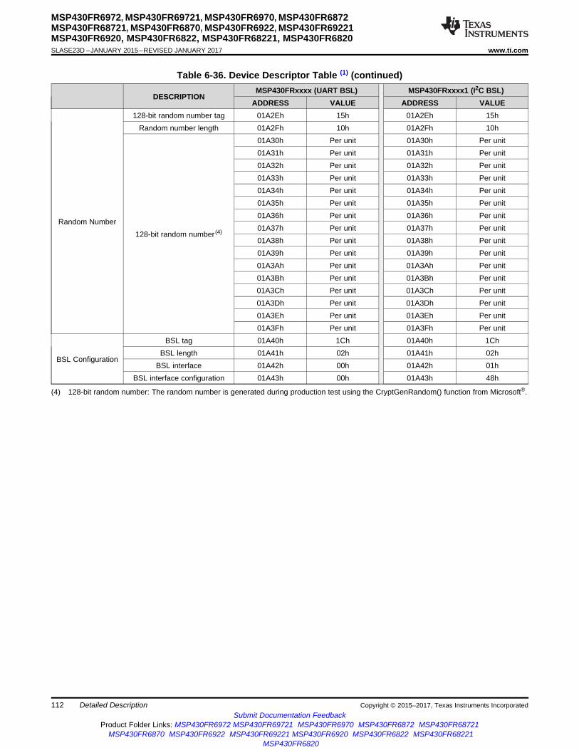
112
MSP430FR6972, MSP430FR69721, MSP430FR6970, MSP430FR6872MSP430FR68721, MSP430FR6870, MSP430FR6922, MSP430FR69221MSP430FR6920, MSP430FR6822, MSP430FR68221, MSP430FR6820SLASE23D –JANUARY 2015–REVISED JANUARY 2017 www.ti.com
Submit Documentation FeedbackProduct Folder Links: MSP430FR6972 MSP430FR69721 MSP430FR6970 MSP430FR6872 MSP430FR68721
MSP430FR6870 MSP430FR6922 MSP430FR69221 MSP430FR6920 MSP430FR6822 MSP430FR68221MSP430FR6820
Detailed Description Copyright © 2015–2017, Texas Instruments Incorporated
Table 6-36. Device Descriptor Table (1) (continued)
DESCRIPTIONMSP430FRxxxx (UART BSL) MSP430FRxxxx1 (I2C BSL)
ADDRESS VALUE ADDRESS VALUE
(4) 128-bit random number: The random number is generated during production test using the CryptGenRandom() function from Microsoft®.
Random Number
128-bit random number tag 01A2Eh 15h 01A2Eh 15hRandom number length 01A2Fh 10h 01A2Fh 10h
128-bit random number (4)
01A30h Per unit 01A30h Per unit01A31h Per unit 01A31h Per unit01A32h Per unit 01A32h Per unit01A33h Per unit 01A33h Per unit01A34h Per unit 01A34h Per unit01A35h Per unit 01A35h Per unit01A36h Per unit 01A36h Per unit01A37h Per unit 01A37h Per unit01A38h Per unit 01A38h Per unit01A39h Per unit 01A39h Per unit01A3Ah Per unit 01A3Ah Per unit01A3Bh Per unit 01A3Bh Per unit01A3Ch Per unit 01A3Ch Per unit01A3Dh Per unit 01A3Dh Per unit01A3Eh Per unit 01A3Eh Per unit01A3Fh Per unit 01A3Fh Per unit
BSL Configuration
BSL tag 01A40h 1Ch 01A40h 1ChBSL length 01A41h 02h 01A41h 02h
BSL interface 01A42h 00h 01A42h 01hBSL interface configuration 01A43h 00h 01A43h 48h

113
MSP430FR6972, MSP430FR69721, MSP430FR6970, MSP430FR6872MSP430FR68721, MSP430FR6870, MSP430FR6922, MSP430FR69221MSP430FR6920, MSP430FR6822, MSP430FR68221, MSP430FR6820
www.ti.com SLASE23D –JANUARY 2015–REVISED JANUARY 2017
Submit Documentation FeedbackProduct Folder Links: MSP430FR6972 MSP430FR69721 MSP430FR6970 MSP430FR6872 MSP430FR68721
MSP430FR6870 MSP430FR6922 MSP430FR69221 MSP430FR6920 MSP430FR6822 MSP430FR68221MSP430FR6820
Detailed DescriptionCopyright © 2015–2017, Texas Instruments Incorporated
(1) All address space not listed is considered vacant memory.(2) Read as: D032h at 00h (Opcode: BIS.W LPM4, SR), 00F0h at 02h (Opcode: BIS.W LPM4, SR), 3FFFh at 04h (Opcode: JMP$)
6.13 MemoryTable 6-37 summarizes the memory map for all devices.
Table 6-37. Memory Organization (1)
MSP430FR69x2(1)MSP430FR68x2(1)
MSP430FR69x0MSP430FR68x0
Memory (FRAM)Main: interrupt vectors andsignaturesMain: code memory
Total Size63KB
00FFFFh–00FF80h013FFFh–004400h
32KB00FFFFh–00FF80h00FF7Fh–008000h
RAM Sect 1 2KB0023FFh–001C00h
2KB0023FFh–001C00h
Device Descriptor Info (TLV)(FRAM)
256 B001AFFh–001A00h
256 B001AFFh–001A00h
Information memory (FRAM)
Info A 128 B0019FFh–001980h
128 B0019FFh–001980h
Info B 128 B00197Fh–001900h
128 B00197Fh–001900h
Info C 128 B0018FFh–001880h
128 B0018FFh–001880h
Info D 128 B00187Fh–001800h
128 B00187Fh–001800h
Bootloader (BSL) memory (ROM)
BSL 3 512 B0017FFh–001600h
512 B0017FFh–001600h
BSL 2 512 B0015FFh–001400h
512 B0015FFh–001400h
BSL 1 512 B0013FFh–001200h
512 B0013FFh–001200h
BSL 0 512 B0011FFh–001000h
512 B0011FFh–001000h
Peripherals Size 4KB000FFFh–000020h
4KB000FFFh–000020h
Tiny RAM Size 26 B000001Fh–000006h
26 B000001Fh–000006h
Reserved(Read Only) (2) Size 6 B
000005h–000000h6 B
000005h–000000h

114
MSP430FR6972, MSP430FR69721, MSP430FR6970, MSP430FR6872MSP430FR68721, MSP430FR6870, MSP430FR6922, MSP430FR69221MSP430FR6920, MSP430FR6822, MSP430FR68221, MSP430FR6820SLASE23D –JANUARY 2015–REVISED JANUARY 2017 www.ti.com
Submit Documentation FeedbackProduct Folder Links: MSP430FR6972 MSP430FR69721 MSP430FR6970 MSP430FR6872 MSP430FR68721
MSP430FR6870 MSP430FR6922 MSP430FR69221 MSP430FR6920 MSP430FR6822 MSP430FR68221MSP430FR6820
Detailed Description Copyright © 2015–2017, Texas Instruments Incorporated
6.13.1 Peripheral File MapTable 6-38 lists the base address and offset range for the registers of supported peripheral modules.
Table 6-38. Peripherals
MODULE NAME BASE ADDRESS OFFSET ADDRESSRANGE
Special Functions (see Table 6-39) 0100h 000h-01FhPMM (see Table 6-40) 0120h 000h-01Fh
FRAM Control (see Table 6-41) 0140h 000h-00FhCRC16 (see Table 6-42) 0150h 000h-007h
RAM Controller (see Table 6-43) 0158h 000h-001hWatchdog (see Table 6-44) 015Ch 000h-001h
CS (see Table 6-45) 0160h 000h-00FhSYS (see Table 6-46) 0180h 000h-01Fh
Shared Reference (see Table 6-47) 01B0h 000h-001hPort P1, P2 (see Table 6-48) 0200h 000h-01FhPort P3, P4 (see Table 6-49) 0220h 000h-01FhPort P5, P6 (see Table 6-50) 0240h 000h-01Fh
Port P7 (see Table 6-51) 0260h 000h-01FhPort P9 (see Table 6-52) 0280h 000h-01FhPort PJ (see Table 6-53) 0320h 000h-01Fh
Timer_A TA0 (see Table 6-54) 0340h 000h-02FhTimer_A TA1 (see Table 6-55) 0380h 000h-02FhTimer_B TB0 (see Table 6-56) 03C0h 000h-02FhTimer_A TA2 (see Table 6-57) 0400h 000h-02Fh
Capacitive Touch I/O 0 (see Table 6-58) 0430h 000h-00FhTimer_A TA3 (see Table 6-59) 0440h 000h-02Fh
Capacitive Touch I/O 1 (see Table 6-60) 0470h 000h-00FhReal-Time Clock (RTC_C) (see Table 6-61) 04A0h 000h-01Fh32-Bit Hardware Multiplier (see Table 6-62) 04C0h 000h-02Fh
DMA General Control (see Table 6-63) 0500h 000h-00FhDMA Channel 0 (see Table 6-63) 0510h 000h-00FhDMA Channel 1 (see Table 6-63) 0520h 000h-00FhDMA Channel 2 (see Table 6-63) 0530h 000h-00Fh
MPU Control (see Table 6-64) 05A0h 000h-00FheUSCI_A0 (see Table 6-65) 05C0h 000h-01FheUSCI_A1 (see Table 6-66) 05E0h 000h-01FheUSCI_B0 (see Table 6-67) 0640h 000h-02FheUSCI_B1 (see Table 6-68) 0680h 000h-02FhADC12_B (see Table 6-69) 0800h 000h-09Fh
Comparator_E (see Table 6-70) 08C0h 000h-00FhCRC32 (see Table 6-71) 0980h 000h-02Fh
AES (see Table 6-72) 09C0h 000h-00FhLCD_C (see Table 6-73) 0A00h 000h-05Fh
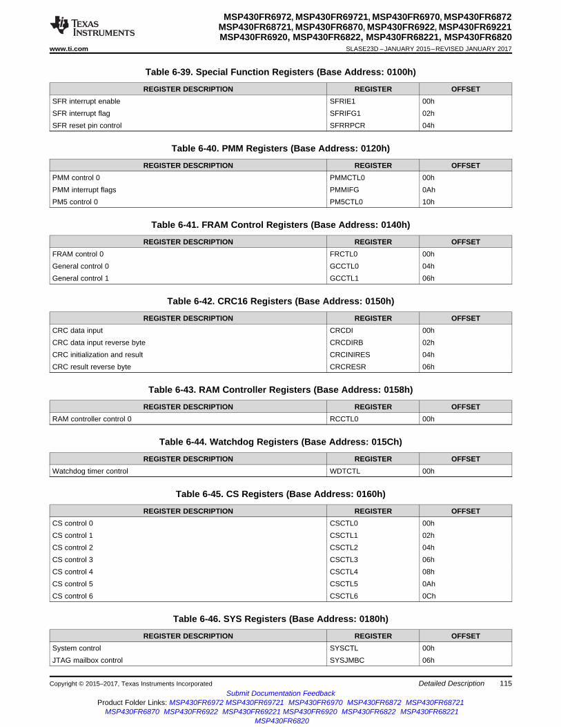
115
MSP430FR6972, MSP430FR69721, MSP430FR6970, MSP430FR6872MSP430FR68721, MSP430FR6870, MSP430FR6922, MSP430FR69221MSP430FR6920, MSP430FR6822, MSP430FR68221, MSP430FR6820
www.ti.com SLASE23D –JANUARY 2015–REVISED JANUARY 2017
Submit Documentation FeedbackProduct Folder Links: MSP430FR6972 MSP430FR69721 MSP430FR6970 MSP430FR6872 MSP430FR68721
MSP430FR6870 MSP430FR6922 MSP430FR69221 MSP430FR6920 MSP430FR6822 MSP430FR68221MSP430FR6820
Detailed DescriptionCopyright © 2015–2017, Texas Instruments Incorporated
Table 6-39. Special Function Registers (Base Address: 0100h)
REGISTER DESCRIPTION REGISTER OFFSETSFR interrupt enable SFRIE1 00hSFR interrupt flag SFRIFG1 02hSFR reset pin control SFRRPCR 04h
Table 6-40. PMM Registers (Base Address: 0120h)
REGISTER DESCRIPTION REGISTER OFFSETPMM control 0 PMMCTL0 00hPMM interrupt flags PMMIFG 0AhPM5 control 0 PM5CTL0 10h
Table 6-41. FRAM Control Registers (Base Address: 0140h)
REGISTER DESCRIPTION REGISTER OFFSETFRAM control 0 FRCTL0 00hGeneral control 0 GCCTL0 04hGeneral control 1 GCCTL1 06h
Table 6-42. CRC16 Registers (Base Address: 0150h)
REGISTER DESCRIPTION REGISTER OFFSETCRC data input CRCDI 00hCRC data input reverse byte CRCDIRB 02hCRC initialization and result CRCINIRES 04hCRC result reverse byte CRCRESR 06h
Table 6-43. RAM Controller Registers (Base Address: 0158h)
REGISTER DESCRIPTION REGISTER OFFSETRAM controller control 0 RCCTL0 00h
Table 6-44. Watchdog Registers (Base Address: 015Ch)
REGISTER DESCRIPTION REGISTER OFFSETWatchdog timer control WDTCTL 00h
Table 6-45. CS Registers (Base Address: 0160h)
REGISTER DESCRIPTION REGISTER OFFSETCS control 0 CSCTL0 00hCS control 1 CSCTL1 02hCS control 2 CSCTL2 04hCS control 3 CSCTL3 06hCS control 4 CSCTL4 08hCS control 5 CSCTL5 0AhCS control 6 CSCTL6 0Ch
Table 6-46. SYS Registers (Base Address: 0180h)
REGISTER DESCRIPTION REGISTER OFFSETSystem control SYSCTL 00hJTAG mailbox control SYSJMBC 06h

116
MSP430FR6972, MSP430FR69721, MSP430FR6970, MSP430FR6872MSP430FR68721, MSP430FR6870, MSP430FR6922, MSP430FR69221MSP430FR6920, MSP430FR6822, MSP430FR68221, MSP430FR6820SLASE23D –JANUARY 2015–REVISED JANUARY 2017 www.ti.com
Submit Documentation FeedbackProduct Folder Links: MSP430FR6972 MSP430FR69721 MSP430FR6970 MSP430FR6872 MSP430FR68721
MSP430FR6870 MSP430FR6922 MSP430FR69221 MSP430FR6920 MSP430FR6822 MSP430FR68221MSP430FR6820
Detailed Description Copyright © 2015–2017, Texas Instruments Incorporated
Table 6-46. SYS Registers (Base Address: 0180h) (continued)REGISTER DESCRIPTION REGISTER OFFSET
JTAG mailbox input 0 SYSJMBI0 08hJTAG mailbox input 1 SYSJMBI1 0AhJTAG mailbox output 0 SYSJMBO0 0ChJTAG mailbox output 1 SYSJMBO1 0EhUser NMI vector generator SYSUNIV 1AhSystem NMI vector generator SYSSNIV 1ChReset vector generator SYSRSTIV 1Eh
Table 6-47. Shared Reference Registers (Base Address: 01B0h)
REGISTER DESCRIPTION REGISTER OFFSETShared reference control REFCTL 00h
Table 6-48. Port P1, P2 Registers (Base Address: 0200h)
REGISTER DESCRIPTION REGISTER OFFSETPort P1 input P1IN 00hPort P1 output P1OUT 02hPort P1 direction P1DIR 04hPort P1 resistor enable P1REN 06hPort P1 selection 0 P1SEL0 0AhPort P1 selection 1 P1SEL1 0ChPort P1 interrupt vector word P1IV 0EhPort P1 complement selection P1SELC 16hPort P1 interrupt edge select P1IES 18hPort P1 interrupt enable P1IE 1AhPort P1 interrupt flag P1IFG 1ChPort P2 input P2IN 01hPort P2 output P2OUT 03hPort P2 direction P2DIR 05hPort P2 resistor enable P2REN 07hPort P2 selection 0 P2SEL0 0BhPort P2 selection 1 P2SEL1 0DhPort P2 complement selection P2SELC 17hPort P2 interrupt vector word P2IV 1EhPort P2 interrupt edge select P2IES 19hPort P2 interrupt enable P2IE 1BhPort P2 interrupt flag P2IFG 1Dh
Table 6-49. Port P3, P4 Registers (Base Address: 0220h)
REGISTER DESCRIPTION REGISTER OFFSETPort P3 input P3IN 00hPort P3 output P3OUT 02hPort P3 direction P3DIR 04hPort P3 resistor enable P3REN 06hPort P3 selection 0 P3SEL0 0AhPort P3 selection 1 P3SEL1 0ChPort P3 interrupt vector word P3IV 0Eh

117
MSP430FR6972, MSP430FR69721, MSP430FR6970, MSP430FR6872MSP430FR68721, MSP430FR6870, MSP430FR6922, MSP430FR69221MSP430FR6920, MSP430FR6822, MSP430FR68221, MSP430FR6820
www.ti.com SLASE23D –JANUARY 2015–REVISED JANUARY 2017
Submit Documentation FeedbackProduct Folder Links: MSP430FR6972 MSP430FR69721 MSP430FR6970 MSP430FR6872 MSP430FR68721
MSP430FR6870 MSP430FR6922 MSP430FR69221 MSP430FR6920 MSP430FR6822 MSP430FR68221MSP430FR6820
Detailed DescriptionCopyright © 2015–2017, Texas Instruments Incorporated
Table 6-49. Port P3, P4 Registers (Base Address: 0220h) (continued)REGISTER DESCRIPTION REGISTER OFFSET
Port P3 complement selection P3SELC 16hPort P3 interrupt edge select P3IES 18hPort P3 interrupt enable P3IE 1AhPort P3 interrupt flag P3IFG 1ChPort P4 input P4IN 01hPort P4 output P4OUT 03hPort P4 direction P4DIR 05hPort P4 resistor enable P4REN 07hPort P4 selection 0 P4SEL0 0BhPort P4 selection 1 P4SEL1 0DhPort P4 complement selection P4SELC 17hPort P4 interrupt vector word P4IV 1EhPort P4 interrupt edge select P4IES 19hPort P4 interrupt enable P4IE 1BhPort P4 interrupt flag P4IFG 1Dh
Table 6-50. Port P5, P6 Registers (Base Address: 0240h)
REGISTER DESCRIPTION REGISTER OFFSETPort P5 input P5IN 00hPort P5 output P5OUT 02hPort P5 direction P5DIR 04hPort P5 resistor enable P5REN 06hPort P5 selection 0 P5SEL0 0AhPort P5 selection 1 P5SEL1 0ChReserved 0EhPort P5 complement selection P5SELC 16hReserved 18hReserved 1AhReserved 1ChPort P6 input P6IN 01hPort P6 output P6OUT 03hPort P6 direction P6DIR 05hPort P6 resistor enable P6REN 07hPort P6 selection 0 P6SEL0 0BhPort P6 selection 1 P6SEL1 0DhPort P6 complement selection P6SELC 17hReserved 1EhReserved 19hReserved 1BhReserved 1Dh
Table 6-51. Port P7 Registers (Base Address: 0260h)
REGISTER DESCRIPTION REGISTER OFFSETPort P7 input P7IN 00hPort P7 output P7OUT 02hPort P7 direction P7DIR 04hPort P7 resistor enable P7REN 06h

118
MSP430FR6972, MSP430FR69721, MSP430FR6970, MSP430FR6872MSP430FR68721, MSP430FR6870, MSP430FR6922, MSP430FR69221MSP430FR6920, MSP430FR6822, MSP430FR68221, MSP430FR6820SLASE23D –JANUARY 2015–REVISED JANUARY 2017 www.ti.com
Submit Documentation FeedbackProduct Folder Links: MSP430FR6972 MSP430FR69721 MSP430FR6970 MSP430FR6872 MSP430FR68721
MSP430FR6870 MSP430FR6922 MSP430FR69221 MSP430FR6920 MSP430FR6822 MSP430FR68221MSP430FR6820
Detailed Description Copyright © 2015–2017, Texas Instruments Incorporated
Table 6-51. Port P7 Registers (Base Address: 0260h) (continued)REGISTER DESCRIPTION REGISTER OFFSET
Port P7 selection 0 P7SEL0 0AhPort P7 selection 1 P7SEL1 0ChReserved 0EhPort P7 complement selection P7SELC 16hReserved 18hReserved 1AhReserved 1Ch
Table 6-52. Port P9 Registers (Base Address: 0280h)
REGISTER DESCRIPTION REGISTER OFFSETPort P9 input P9IN 00hPort P9 output P9OUT 02hPort P9 direction P9DIR 04hPort P9 resistor enable P9REN 06hPort P9 selection 0 P9SEL0 0AhPort P9 selection 1 P9SEL1 0ChReserved 0EhPort P9 complement selection P9SELC 16hReserved 18hReserved 1AhReserved 1Ch
Table 6-53. Port J Registers (Base Address: 0320h)
REGISTER DESCRIPTION REGISTER OFFSETPort PJ input PJIN 00hPort PJ output PJOUT 02hPort PJ direction PJDIR 04hPort PJ resistor enable PJREN 06hPort PJ selection 0 PJSEL0 0AhPort PJ selection 1 PJSEL1 0ChPort PJ complement selection PJSELC 16h
Table 6-54. Timer_A TA0 Registers (Base Address: 0340h)
REGISTER DESCRIPTION REGISTER OFFSETTA0 control TA0CTL 00hCapture/compare control 0 TA0CCTL0 02hCapture/compare control 1 TA0CCTL1 04hCapture/compare control 2 TA0CCTL2 06hTA0 counter TA0R 10hCapture/compare 0 TA0CCR0 12hCapture/compare 1 TA0CCR1 14hCapture/compare 2 TA0CCR2 16hTA0 expansion 0 TA0EX0 20hTA0 interrupt vector TA0IV 2Eh
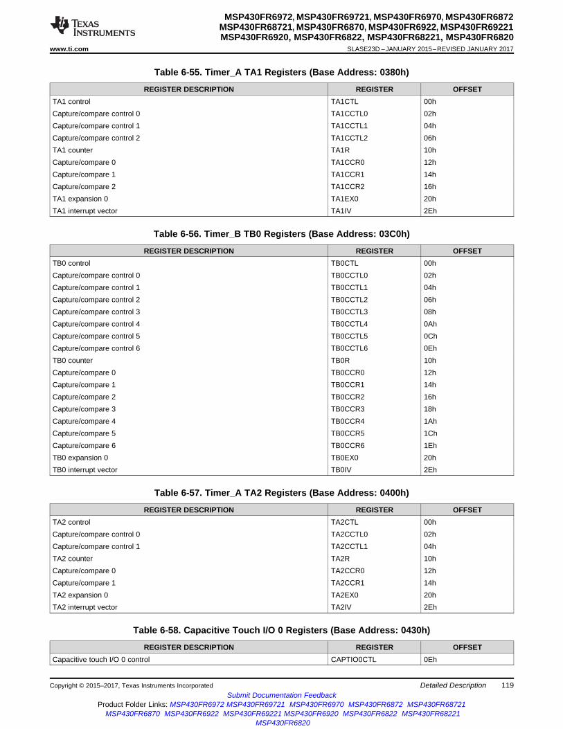
119
MSP430FR6972, MSP430FR69721, MSP430FR6970, MSP430FR6872MSP430FR68721, MSP430FR6870, MSP430FR6922, MSP430FR69221MSP430FR6920, MSP430FR6822, MSP430FR68221, MSP430FR6820
www.ti.com SLASE23D –JANUARY 2015–REVISED JANUARY 2017
Submit Documentation FeedbackProduct Folder Links: MSP430FR6972 MSP430FR69721 MSP430FR6970 MSP430FR6872 MSP430FR68721
MSP430FR6870 MSP430FR6922 MSP430FR69221 MSP430FR6920 MSP430FR6822 MSP430FR68221MSP430FR6820
Detailed DescriptionCopyright © 2015–2017, Texas Instruments Incorporated
Table 6-55. Timer_A TA1 Registers (Base Address: 0380h)
REGISTER DESCRIPTION REGISTER OFFSETTA1 control TA1CTL 00hCapture/compare control 0 TA1CCTL0 02hCapture/compare control 1 TA1CCTL1 04hCapture/compare control 2 TA1CCTL2 06hTA1 counter TA1R 10hCapture/compare 0 TA1CCR0 12hCapture/compare 1 TA1CCR1 14hCapture/compare 2 TA1CCR2 16hTA1 expansion 0 TA1EX0 20hTA1 interrupt vector TA1IV 2Eh
Table 6-56. Timer_B TB0 Registers (Base Address: 03C0h)
REGISTER DESCRIPTION REGISTER OFFSETTB0 control TB0CTL 00hCapture/compare control 0 TB0CCTL0 02hCapture/compare control 1 TB0CCTL1 04hCapture/compare control 2 TB0CCTL2 06hCapture/compare control 3 TB0CCTL3 08hCapture/compare control 4 TB0CCTL4 0AhCapture/compare control 5 TB0CCTL5 0ChCapture/compare control 6 TB0CCTL6 0EhTB0 counter TB0R 10hCapture/compare 0 TB0CCR0 12hCapture/compare 1 TB0CCR1 14hCapture/compare 2 TB0CCR2 16hCapture/compare 3 TB0CCR3 18hCapture/compare 4 TB0CCR4 1AhCapture/compare 5 TB0CCR5 1ChCapture/compare 6 TB0CCR6 1EhTB0 expansion 0 TB0EX0 20hTB0 interrupt vector TB0IV 2Eh
Table 6-57. Timer_A TA2 Registers (Base Address: 0400h)
REGISTER DESCRIPTION REGISTER OFFSETTA2 control TA2CTL 00hCapture/compare control 0 TA2CCTL0 02hCapture/compare control 1 TA2CCTL1 04hTA2 counter TA2R 10hCapture/compare 0 TA2CCR0 12hCapture/compare 1 TA2CCR1 14hTA2 expansion 0 TA2EX0 20hTA2 interrupt vector TA2IV 2Eh
Table 6-58. Capacitive Touch I/O 0 Registers (Base Address: 0430h)
REGISTER DESCRIPTION REGISTER OFFSETCapacitive touch I/O 0 control CAPTIO0CTL 0Eh

120
MSP430FR6972, MSP430FR69721, MSP430FR6970, MSP430FR6872MSP430FR68721, MSP430FR6870, MSP430FR6922, MSP430FR69221MSP430FR6920, MSP430FR6822, MSP430FR68221, MSP430FR6820SLASE23D –JANUARY 2015–REVISED JANUARY 2017 www.ti.com
Submit Documentation FeedbackProduct Folder Links: MSP430FR6972 MSP430FR69721 MSP430FR6970 MSP430FR6872 MSP430FR68721
MSP430FR6870 MSP430FR6922 MSP430FR69221 MSP430FR6920 MSP430FR6822 MSP430FR68221MSP430FR6820
Detailed Description Copyright © 2015–2017, Texas Instruments Incorporated
Table 6-59. Timer_A TA3 Registers (Base Address: 0440h)
REGISTER DESCRIPTION REGISTER OFFSETTA3 control TA3CTL 00hCapture/compare control 0 TA3CCTL0 02hCapture/compare control 1 TA3CCTL1 04hCapture/compare control 2 TA3CCTL2 06hCapture/compare control 3 TA3CCTL3 08hCapture/compare control 4 TA3CCTL4 0AhTA3 counter TA3R 10hCapture/compare 0 TA3CCR0 12hCapture/compare 1 TA3CCR1 14hCapture/compare 2 TA3CCR2 16hCapture/compare 3 TA3CCR3 18hCapture/compare 4 TA3CCR4 1AhTA3 expansion 0 TA3EX0 20hTA3 interrupt vector TA3IV 2Eh
Table 6-60. Capacitive Touch I/O 1 Registers (Base Address: 0470h)
REGISTER DESCRIPTION REGISTER OFFSETCapacitive touch I/O 1 control CAPTIO1CTL 0Eh
Table 6-61. RTC_C Registers (Base Address: 04A0h)
REGISTER DESCRIPTION REGISTER OFFSETRTC control 0 RTCCTL0 00hRTC password RTCPWD 01hRTC control 1 RTCCTL1 02hRTC control 3 RTCCTL3 03hRTC offset calibration RTCOCAL 04hRTC temperature compensation RTCTCMP 06hRTC prescaler 0 control RTCPS0CTL 08hRTC prescaler 1 control RTCPS1CTL 0AhRTC prescaler 0 RTCPS0 0ChRTC prescaler 1 RTCPS1 0DhRTC interrupt vector word RTCIV 0EhRTC seconds/counter 1 RTCSEC/RTCNT1 10hRTC minutes/counter 2 RTCMIN/RTCNT2 11hRTC hours/counter 3 RTCHOUR/RTCNT3 12hRTC day of week/counter 4 RTCDOW/RTCNT4 13hRTC days RTCDAY 14hRTC month RTCMON 15hRTC year RTCYEAR 16hRTC alarm minutes RTCAMIN 18hRTC alarm hours RTCAHOUR 19hRTC alarm day of week RTCADOW 1AhRTC alarm days RTCADAY 1BhBinary-to-BCD conversion BIN2BCD 1ChBCD-to-binary conversion BCD2BIN 1Eh
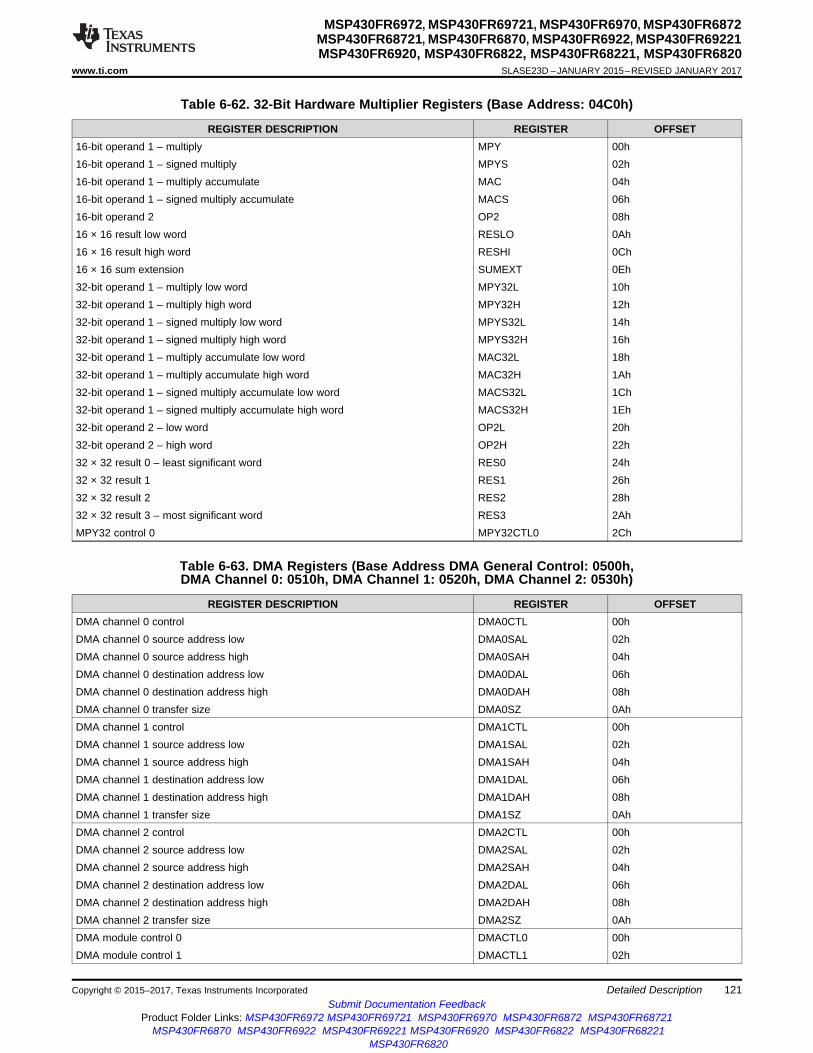
121
MSP430FR6972, MSP430FR69721, MSP430FR6970, MSP430FR6872MSP430FR68721, MSP430FR6870, MSP430FR6922, MSP430FR69221MSP430FR6920, MSP430FR6822, MSP430FR68221, MSP430FR6820
www.ti.com SLASE23D –JANUARY 2015–REVISED JANUARY 2017
Submit Documentation FeedbackProduct Folder Links: MSP430FR6972 MSP430FR69721 MSP430FR6970 MSP430FR6872 MSP430FR68721
MSP430FR6870 MSP430FR6922 MSP430FR69221 MSP430FR6920 MSP430FR6822 MSP430FR68221MSP430FR6820
Detailed DescriptionCopyright © 2015–2017, Texas Instruments Incorporated
Table 6-62. 32-Bit Hardware Multiplier Registers (Base Address: 04C0h)
REGISTER DESCRIPTION REGISTER OFFSET16-bit operand 1 – multiply MPY 00h16-bit operand 1 – signed multiply MPYS 02h16-bit operand 1 – multiply accumulate MAC 04h16-bit operand 1 – signed multiply accumulate MACS 06h16-bit operand 2 OP2 08h16 × 16 result low word RESLO 0Ah16 × 16 result high word RESHI 0Ch16 × 16 sum extension SUMEXT 0Eh32-bit operand 1 – multiply low word MPY32L 10h32-bit operand 1 – multiply high word MPY32H 12h32-bit operand 1 – signed multiply low word MPYS32L 14h32-bit operand 1 – signed multiply high word MPYS32H 16h32-bit operand 1 – multiply accumulate low word MAC32L 18h32-bit operand 1 – multiply accumulate high word MAC32H 1Ah32-bit operand 1 – signed multiply accumulate low word MACS32L 1Ch32-bit operand 1 – signed multiply accumulate high word MACS32H 1Eh32-bit operand 2 – low word OP2L 20h32-bit operand 2 – high word OP2H 22h32 × 32 result 0 – least significant word RES0 24h32 × 32 result 1 RES1 26h32 × 32 result 2 RES2 28h32 × 32 result 3 – most significant word RES3 2AhMPY32 control 0 MPY32CTL0 2Ch
Table 6-63. DMA Registers (Base Address DMA General Control: 0500h,DMA Channel 0: 0510h, DMA Channel 1: 0520h, DMA Channel 2: 0530h)
REGISTER DESCRIPTION REGISTER OFFSETDMA channel 0 control DMA0CTL 00hDMA channel 0 source address low DMA0SAL 02hDMA channel 0 source address high DMA0SAH 04hDMA channel 0 destination address low DMA0DAL 06hDMA channel 0 destination address high DMA0DAH 08hDMA channel 0 transfer size DMA0SZ 0AhDMA channel 1 control DMA1CTL 00hDMA channel 1 source address low DMA1SAL 02hDMA channel 1 source address high DMA1SAH 04hDMA channel 1 destination address low DMA1DAL 06hDMA channel 1 destination address high DMA1DAH 08hDMA channel 1 transfer size DMA1SZ 0AhDMA channel 2 control DMA2CTL 00hDMA channel 2 source address low DMA2SAL 02hDMA channel 2 source address high DMA2SAH 04hDMA channel 2 destination address low DMA2DAL 06hDMA channel 2 destination address high DMA2DAH 08hDMA channel 2 transfer size DMA2SZ 0AhDMA module control 0 DMACTL0 00hDMA module control 1 DMACTL1 02h

122
MSP430FR6972, MSP430FR69721, MSP430FR6970, MSP430FR6872MSP430FR68721, MSP430FR6870, MSP430FR6922, MSP430FR69221MSP430FR6920, MSP430FR6822, MSP430FR68221, MSP430FR6820SLASE23D –JANUARY 2015–REVISED JANUARY 2017 www.ti.com
Submit Documentation FeedbackProduct Folder Links: MSP430FR6972 MSP430FR69721 MSP430FR6970 MSP430FR6872 MSP430FR68721
MSP430FR6870 MSP430FR6922 MSP430FR69221 MSP430FR6920 MSP430FR6822 MSP430FR68221MSP430FR6820
Detailed Description Copyright © 2015–2017, Texas Instruments Incorporated
Table 6-63. DMA Registers (Base Address DMA General Control: 0500h,DMA Channel 0: 0510h, DMA Channel 1: 0520h, DMA Channel 2: 0530h) (continued)
REGISTER DESCRIPTION REGISTER OFFSETDMA module control 2 DMACTL2 04hDMA module control 3 DMACTL3 06hDMA module control 4 DMACTL4 08hDMA interrupt vector DMAIV 0Eh
Table 6-64. MPU Control Registers (Base Address: 05A0h)
REGISTER DESCRIPTION REGISTER OFFSETMPU control 0 MPUCTL0 00hMPU control 1 MPUCTL1 02hMPU Segmentation Border 2 MPUSEGB2 04hMPU Segmentation Border 1 MPUSEGB1 06hMPU access management MPUSAM 08hMPU IP control 0 MPUIPC0 0AhMPU IP Encapsulation Segment Border 2 MPUIPSEGB2 0ChMPU IP Encapsulation Segment Border 1 MPUIPSEGB1 0Eh
Table 6-65. eUSCI_A0 Registers (Base Address: 05C0h)
REGISTER DESCRIPTION REGISTER OFFSETeUSCI_A control word 0 UCA0CTLW0 00heUSCI _A control word 1 UCA0CTLW1 02heUSCI_A baud rate 0 UCA0BR0 06heUSCI_A baud rate 1 UCA0BR1 07heUSCI_A modulation control UCA0MCTLW 08heUSCI_A status word UCA0STATW 0AheUSCI_A receive buffer UCA0RXBUF 0CheUSCI_A transmit buffer UCA0TXBUF 0EheUSCI_A LIN control UCA0ABCTL 10heUSCI_A IrDA transmit control UCA0IRTCTL 12heUSCI_A IrDA receive control UCA0IRRCTL 13heUSCI_A interrupt enable UCA0IE 1AheUSCI_A interrupt flags UCA0IFG 1CheUSCI_A interrupt vector word UCA0IV 1Eh
Table 6-66. eUSCI_A1 Registers (Base Address:05E0h)
REGISTER DESCRIPTION REGISTER OFFSETeUSCI_A control word 0 UCA1CTLW0 00heUSCI _A control word 1 UCA1CTLW1 02heUSCI_A baud rate 0 UCA1BR0 06heUSCI_A baud rate 1 UCA1BR1 07heUSCI_A modulation control UCA1MCTLW 08heUSCI_A status word UCA1STATW 0AheUSCI_A receive buffer UCA1RXBUF 0CheUSCI_A transmit buffer UCA1TXBUF 0EheUSCI_A LIN control UCA1ABCTL 10heUSCI_A IrDA transmit control UCA1IRTCTL 12h

123
MSP430FR6972, MSP430FR69721, MSP430FR6970, MSP430FR6872MSP430FR68721, MSP430FR6870, MSP430FR6922, MSP430FR69221MSP430FR6920, MSP430FR6822, MSP430FR68221, MSP430FR6820
www.ti.com SLASE23D –JANUARY 2015–REVISED JANUARY 2017
Submit Documentation FeedbackProduct Folder Links: MSP430FR6972 MSP430FR69721 MSP430FR6970 MSP430FR6872 MSP430FR68721
MSP430FR6870 MSP430FR6922 MSP430FR69221 MSP430FR6920 MSP430FR6822 MSP430FR68221MSP430FR6820
Detailed DescriptionCopyright © 2015–2017, Texas Instruments Incorporated
Table 6-66. eUSCI_A1 Registers (Base Address:05E0h) (continued)REGISTER DESCRIPTION REGISTER OFFSET
eUSCI_A IrDA receive control UCA1IRRCTL 13heUSCI_A interrupt enable UCA1IE 1AheUSCI_A interrupt flags UCA1IFG 1CheUSCI_A interrupt vector word UCA1IV 1Eh
Table 6-67. eUSCI_B0 Registers (Base Address: 0640h)
REGISTER DESCRIPTION REGISTER OFFSETeUSCI_B control word 0 UCB0CTLW0 00heUSCI_B control word 1 UCB0CTLW1 02heUSCI_B bit rate 0 UCB0BR0 06heUSCI_B bit rate 1 UCB0BR1 07heUSCI_B status word UCB0STATW 08heUSCI_B byte counter threshold UCB0TBCNT 0AheUSCI_B receive buffer UCB0RXBUF 0CheUSCI_B transmit buffer UCB0TXBUF 0EheUSCI_B I2C own address 0 UCB0I2COA0 14heUSCI_B I2C own address 1 UCB0I2COA1 16heUSCI_B I2C own address 2 UCB0I2COA2 18heUSCI_B I2C own address 3 UCB0I2COA3 1AheUSCI_B received address UCB0ADDRX 1CheUSCI_B address mask UCB0ADDMASK 1EheUSCI_B I2C slave address UCB0I2CSA 20heUSCI_B interrupt enable UCB0IE 2AheUSCI_B interrupt flags UCB0IFG 2CheUSCI_B interrupt vector word UCB0IV 2Eh
Table 6-68. eUSCI_B1 Registers (Base Address: 0680h)
REGISTER DESCRIPTION REGISTER OFFSETeUSCI_B control word 0 UCB1CTLW0 00heUSCI_B control word 1 UCB1CTLW1 02heUSCI_B bit rate 0 UCB1BR0 06heUSCI_B bit rate 1 UCB1BR1 07heUSCI_B status word UCB1STATW 08heUSCI_B byte counter threshold UCB1TBCNT 0AheUSCI_B receive buffer UCB1RXBUF 0CheUSCI_B transmit buffer UCB1TXBUF 0EheUSCI_B I2C own address 0 UCB1I2COA0 14heUSCI_B I2C own address 1 UCB1I2COA1 16heUSCI_B I2C own address 2 UCB1I2COA2 18heUSCI_B I2C own address 3 UCB1I2COA3 1AheUSCI_B received address UCB1ADDRX 1CheUSCI_B address mask UCB1ADDMASK 1EheUSCI_B I2C slave address UCB1I2CSA 20heUSCI_B interrupt enable UCB1IE 2AheUSCI_B interrupt flags UCB1IFG 2CheUSCI_B interrupt vector word UCB1IV 2Eh

124
MSP430FR6972, MSP430FR69721, MSP430FR6970, MSP430FR6872MSP430FR68721, MSP430FR6870, MSP430FR6922, MSP430FR69221MSP430FR6920, MSP430FR6822, MSP430FR68221, MSP430FR6820SLASE23D –JANUARY 2015–REVISED JANUARY 2017 www.ti.com
Submit Documentation FeedbackProduct Folder Links: MSP430FR6972 MSP430FR69721 MSP430FR6970 MSP430FR6872 MSP430FR68721
MSP430FR6870 MSP430FR6922 MSP430FR69221 MSP430FR6920 MSP430FR6822 MSP430FR68221MSP430FR6820
Detailed Description Copyright © 2015–2017, Texas Instruments Incorporated
Table 6-69. ADC12_B Registers (Base Address: 0800h)
REGISTER DESCRIPTION REGISTER OFFSETADC12_B control 0 ADC12CTL0 00hADC12_B control 1 ADC12CTL1 02hADC12_B control 2 ADC12CTL2 04hADC12_B control 3 ADC12CTL3 06hADC12_B window comparator low threshold ADC12LO 08hADC12_B window comparator high threshold ADC12HI 0AhADC12_B interrupt flag 0 ADC12IFGR0 0ChADC12_B interrupt flag 1 ADC12IFGR1 0EhADC12_B interrupt flag 2 ADC12IFGR2 10hADC12_B interrupt enable 0 ADC12IER0 12hADC12_B Interrupt Enable 1 ADC12IER1 14hADC12_B interrupt enable 2 ADC12IER2 16hADC12_B interrupt vector ADC12IV 18hADC12_B memory control 0 ADC12MCTL0 20hADC12_B memory control 1 ADC12MCTL1 22hADC12_B memory control 2 ADC12MCTL2 24hADC12_B memory control 3 ADC12MCTL3 26hADC12_B memory control 4 ADC12MCTL4 28hADC12_B memory control 5 ADC12MCTL5 2AhADC12_B memory control 6 ADC12MCTL6 2ChADC12_B memory control 7 ADC12MCTL7 2EhADC12_B memory control 8 ADC12MCTL8 30hADC12_B memory control 9 ADC12MCTL9 32hADC12_B memory control 10 ADC12MCTL10 34hADC12_B memory control 11 ADC12MCTL11 36hADC12_B memory control 12 ADC12MCTL12 38hADC12_B memory control 13 ADC12MCTL13 3AhADC12_B memory control 14 ADC12MCTL14 3ChADC12_B memory control 15 ADC12MCTL15 3EhADC12_B memory control 16 ADC12MCTL16 40hADC12_B memory control 17 ADC12MCTL17 42hADC12_B memory control 18 ADC12MCTL18 44hADC12_B memory control 19 ADC12MCTL19 46hADC12_B memory control 20 ADC12MCTL20 48hADC12_B memory control 21 ADC12MCTL21 4AhADC12_B memory control 22 ADC12MCTL22 4ChADC12_B memory control 23 ADC12MCTL23 4EhADC12_B memory control 24 ADC12MCTL24 50hADC12_B memory control 25 ADC12MCTL25 52hADC12_B memory control 26 ADC12MCTL26 54hADC12_B memory control 27 ADC12MCTL27 56hADC12_B memory control 28 ADC12MCTL28 58hADC12_B memory control 29 ADC12MCTL29 5AhADC12_B memory control 30 ADC12MCTL30 5ChADC12_B memory control 31 ADC12MCTL31 5EhADC12_B memory 0 ADC12MEM0 60hADC12_B memory 1 ADC12MEM1 62h

125
MSP430FR6972, MSP430FR69721, MSP430FR6970, MSP430FR6872MSP430FR68721, MSP430FR6870, MSP430FR6922, MSP430FR69221MSP430FR6920, MSP430FR6822, MSP430FR68221, MSP430FR6820
www.ti.com SLASE23D –JANUARY 2015–REVISED JANUARY 2017
Submit Documentation FeedbackProduct Folder Links: MSP430FR6972 MSP430FR69721 MSP430FR6970 MSP430FR6872 MSP430FR68721
MSP430FR6870 MSP430FR6922 MSP430FR69221 MSP430FR6920 MSP430FR6822 MSP430FR68221MSP430FR6820
Detailed DescriptionCopyright © 2015–2017, Texas Instruments Incorporated
Table 6-69. ADC12_B Registers (Base Address: 0800h) (continued)REGISTER DESCRIPTION REGISTER OFFSET
ADC12_B memory 2 ADC12MEM2 64hADC12_B memory 3 ADC12MEM3 66hADC12_B memory 4 ADC12MEM4 68hADC12_B memory 5 ADC12MEM5 6AhADC12_B memory 6 ADC12MEM6 6ChADC12_B memory 7 ADC12MEM7 6EhADC12_B memory 8 ADC12MEM8 70hADC12_B memory 9 ADC12MEM9 72hADC12_B memory 10 ADC12MEM10 74hADC12_B memory 11 ADC12MEM11 76hADC12_B memory 12 ADC12MEM12 78hADC12_B memory 13 ADC12MEM13 7AhADC12_B memory 14 ADC12MEM14 7ChADC12_B memory 15 ADC12MEM15 7EhADC12_B memory 16 ADC12MEM16 80hADC12_B memory 17 ADC12MEM17 82hADC12_B memory 18 ADC12MEM18 84hADC12_B memory 19 ADC12MEM19 86hADC12_B memory 20 ADC12MEM20 88hADC12_B memory 21 ADC12MEM21 8AhADC12_B memory 22 ADC12MEM22 8ChADC12_B memory 23 ADC12MEM23 8EhADC12_B memory 24 ADC12MEM24 90hADC12_B memory 25 ADC12MEM25 92hADC12_B memory 26 ADC12MEM26 94hADC12_B memory 27 ADC12MEM27 96hADC12_B memory 28 ADC12MEM28 98hADC12_B memory 29 ADC12MEM29 9AhADC12_B memory 30 ADC12MEM30 9ChADC12_B memory 31 ADC12MEM31 9Eh
Table 6-70. Comparator_E Registers (Base Address: 08C0h)
REGISTER DESCRIPTION REGISTER OFFSETComparator control 0 CECTL0 00hComparator control 1 CECTL1 02hComparator control 2 CECTL2 04hComparator control 3 CECTL3 06hComparator interrupt CEINT 0ChComparator interrupt vector word CEIV 0Eh
Table 6-71. CRC32 Registers (Base Address: 0980h)
REGISTER DESCRIPTION REGISTER OFFSETCRC32 data input CRC32DIW0 00hReserved 02hReserved 04hCRC32 data input reverse CRC32DIRBW0 06hCRC32 initialization and result word 0 CRC32INIRESW0 08h

126
MSP430FR6972, MSP430FR69721, MSP430FR6970, MSP430FR6872MSP430FR68721, MSP430FR6870, MSP430FR6922, MSP430FR69221MSP430FR6920, MSP430FR6822, MSP430FR68221, MSP430FR6820SLASE23D –JANUARY 2015–REVISED JANUARY 2017 www.ti.com
Submit Documentation FeedbackProduct Folder Links: MSP430FR6972 MSP430FR69721 MSP430FR6970 MSP430FR6872 MSP430FR68721
MSP430FR6870 MSP430FR6922 MSP430FR69221 MSP430FR6920 MSP430FR6822 MSP430FR68221MSP430FR6820
Detailed Description Copyright © 2015–2017, Texas Instruments Incorporated
Table 6-71. CRC32 Registers (Base Address: 0980h) (continued)REGISTER DESCRIPTION REGISTER OFFSET
CRC32 initialization and result word 1 CRC32INIRESW1 0AhCRC32 result reverse word 1 CRC32RESRW1 0ChCRC32 result reverse word 0 CRC32RESRW1 0EhCRC16 data input CRC16DIW0 10hReserved 12hReserved 14hCRC16 data input reverse CRC16DIRBW0 16hCRC16 initialization and result word 0 CRC16INIRESW0 18hReserved 1AhReserved 1ChCRC16 result reverse word 0 CRC16RESRW1 1EhReserved 20hReserved 22hReserved 24hReserved 26hReserved 28hReserved 2AhReserved 2ChReserved 2Eh
Table 6-72. AES Accelerator Registers (Base Address: 09C0h)
REGISTER DESCRIPTION REGISTER OFFSETAES accelerator control 0 AESACTL0 00hReserved 02hAES accelerator status AESASTAT 04hAES accelerator key AESAKEY 06hAES accelerator data in AESADIN 008hAES accelerator data out AESADOUT 00AhAES accelerator XORed data in AESAXDIN 00ChAES accelerator XORed data in (no trigger) AESAXIN 00Eh
Table 6-73. LCD_C Registers (Base Address: 0A00h)
REGISTER DESCRIPTION REGISTER OFFSETLCD_C control 0 LCDCCTL0 000hLCD_C control 1 LCDCCTL1 002hLCD_C blinking control LCDCBLKCTL 004hLCD_C memory control LCDCMEMCTL 006hLCD_C voltage control LCDCVCTL 008hLCD_C port control 0 LCDCPCTL0 00AhLCD_C port control 1 LCDCPCTL1 00ChLCD_C port control 2 LCDCPCTL2 00EhLCD_C charge pump control LCDCCPCTL 012hLCD_C interrupt vector LCDCIV 01EhStatic and 2 to 4 mux modesLCD_C memory 1 LCDM1 020hLCD_C memory 2 LCDM2 021hLCD_C memory 3 LCDM3 022h

127
MSP430FR6972, MSP430FR69721, MSP430FR6970, MSP430FR6872MSP430FR68721, MSP430FR6870, MSP430FR6922, MSP430FR69221MSP430FR6920, MSP430FR6822, MSP430FR68221, MSP430FR6820
www.ti.com SLASE23D –JANUARY 2015–REVISED JANUARY 2017
Submit Documentation FeedbackProduct Folder Links: MSP430FR6972 MSP430FR69721 MSP430FR6970 MSP430FR6872 MSP430FR68721
MSP430FR6870 MSP430FR6922 MSP430FR69221 MSP430FR6920 MSP430FR6822 MSP430FR68221MSP430FR6820
Detailed DescriptionCopyright © 2015–2017, Texas Instruments Incorporated
Table 6-73. LCD_C Registers (Base Address: 0A00h) (continued)REGISTER DESCRIPTION REGISTER OFFSET
LCD_C memory 4 LCDM4 023hLCD_C memory 5 LCDM5 024hLCD_C memory 6 LCDM6 025hLCD_C memory 7 LCDM7 026hLCD_C memory 8 LCDM8 027hLCD_C memory 9 LCDM9 028hLCD_C memory 10 LCDM10 029hLCD_C memory 11 LCDM11 02AhLCD_C memory 12 LCDM12 02BhLCD_C memory 13 LCDM13 02ChLCD_C memory 14 LCDM14 02DhLCD_C memory 15 LCDM15 02EhLCD_C memory 16 LCDM16 02FhLCD_C memory 17 LCDM17 030hLCD_C memory 18 LCDM18 031hLCD_C memory 19 LCDM19 032hLCD_C memory 20 LCDM20 033hLCD_C memory 21 LCDM21 034hLCD_C memory 22 LCDM22 035hReserved 036hReserved 037hLCD_C blinking memory 1 LCDBM1 040hLCD_C blinking memory 2 LCDBM2 041hLCD_C blinking memory 3 LCDBM3 042hLCD_C blinking memory 4 LCDBM4 043hLCD_C blinking memory 5 LCDBM5 044hLCD_C blinking memory 6 LCDBM6 045hLCD_C blinking memory 7 LCDBM7 046hLCD_C blinking memory 8 LCDBM8 047hLCD_C blinking memory 9 LCDBM9 048hLCD_C blinking memory 10 LCDBM10 049hLCD_C blinking memory 11 LCDBM11 04AhLCD_C blinking memory 12 LCDBM12 04BhLCD_C blinking memory 13 LCDBM13 04ChLCD_C blinking memory 14 LCDBM14 04DhLCD_C blinking memory 15 LCDBM15 04EhLCD_C blinking memory 16 LCDBM16 04FhLCD_C blinking memory 17 LCDBM17 050hLCD_C blinking memory 18 LCDBM18 051hLCD_C blinking memory 19 LCDBM19 052hLCD_C blinking memory 20 LCDBM20 053hLCD_C blinking memory 21 LCDBM21 054hLCD_C blinking memory 22 LCDBM22 055hReserved 056hReserved 057h5 to 8 mux modesLCD_C memory 1 LCDM1 020h

128
MSP430FR6972, MSP430FR69721, MSP430FR6970, MSP430FR6872MSP430FR68721, MSP430FR6870, MSP430FR6922, MSP430FR69221MSP430FR6920, MSP430FR6822, MSP430FR68221, MSP430FR6820SLASE23D –JANUARY 2015–REVISED JANUARY 2017 www.ti.com
Submit Documentation FeedbackProduct Folder Links: MSP430FR6972 MSP430FR69721 MSP430FR6970 MSP430FR6872 MSP430FR68721
MSP430FR6870 MSP430FR6922 MSP430FR69221 MSP430FR6920 MSP430FR6822 MSP430FR68221MSP430FR6820
Detailed Description Copyright © 2015–2017, Texas Instruments Incorporated
Table 6-73. LCD_C Registers (Base Address: 0A00h) (continued)REGISTER DESCRIPTION REGISTER OFFSET
LCD_C memory 2 LCDM2 021hLCD_C memory 3 LCDM3 022hLCD_C memory 4 LCDM4 023hLCD_C memory 5 LCDM5 024hLCD_C memory 6 LCDM6 025hLCD_C memory 7 LCDM7 026hLCD_C memory 8 LCDM8 027hLCD_C memory 9 LCDM9 028hLCD_C memory 10 LCDM10 029hLCD_C memory 11 LCDM11 02AhLCD_C memory 12 LCDM12 02BhLCD_C memory 13 LCDM13 02ChLCD_C memory 14 LCDM14 02DhLCD_C memory 15 LCDM15 02EhLCD_C memory 16 LCDM16 02FhLCD_C memory 17 LCDM17 030hLCD_C memory 18 LCDM18 031hLCD_C memory 19 LCDM19 032hLCD_C memory 20 LCDM20 033hLCD_C memory 21 LCDM21 034hLCD_C memory 22 LCDM22 035hLCD_C memory 23 LCDM23 036hLCD_C memory 24 LCDM24 037hLCD_C memory 25 LCDM25 038hLCD_C memory 26 LCDM26 039hLCD_C memory 27 LCDM27 03AhLCD_C memory 28 LCDM28 03BhLCD_C memory 29 LCDM29 03ChLCD_C memory 30 LCDM30 03DhLCD_C memory 31 LCDM31 03EhLCD_C memory 32 LCDM32 03FhLCD_C memory 33 LCDM33 040hLCD_C memory 34 LCDM34 041hLCD_C memory 35 LCDM35 042hLCD_C memory 36 LCDM36 043hLCD_C memory 37 LCDM37 044hLCD_C memory 38 LCDM38 045hLCD_C memory 39 LCDM39 046hLCD_C memory 40 LCDM40 047hLCD_C memory 41 LCDM41 048hLCD_C memory 42 LCDM42 049hLCD_C memory 43 LCDM43 04Ah

129
MSP430FR6972, MSP430FR69721, MSP430FR6970, MSP430FR6872MSP430FR68721, MSP430FR6870, MSP430FR6922, MSP430FR69221MSP430FR6920, MSP430FR6822, MSP430FR68221, MSP430FR6820
www.ti.com SLASE23D –JANUARY 2015–REVISED JANUARY 2017
Submit Documentation FeedbackProduct Folder Links: MSP430FR6972 MSP430FR69721 MSP430FR6970 MSP430FR6872 MSP430FR68721
MSP430FR6870 MSP430FR6922 MSP430FR69221 MSP430FR6920 MSP430FR6822 MSP430FR68221MSP430FR6820
Detailed DescriptionCopyright © 2015–2017, Texas Instruments Incorporated
6.14 Identification
6.14.1 Revision IdentificationThe device revision information is shown as part of the top-side marking on the device package. Thedevice-specific errata sheet describes these markings. For links to the errata sheets for the devices in thisdata sheet, see Section 8.4.
The hardware revision is also stored in the Device Descriptor structure in the Info Block section. Fordetails on this value, see the "Hardware Revision" entries in Section 6.12.
6.14.2 Device IdentificationThe device type can be identified from the top-side marking on the device package. The device-specificerrata sheet describes these markings. For links to the errata sheets for the devices in this data sheet, seeSection 8.4.
A device identification value is also stored in the Device Descriptor structure in the Info Block section. Fordetails on this value, see the "Device ID" entries in Section 6.12.
6.14.3 JTAG IdentificationProgramming through the JTAG interface, including reading and identifying the JTAG ID, is described indetail in MSP430 Programming With the JTAG Interface.
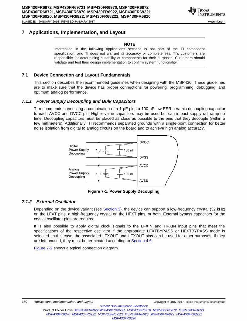
DigitalPower SupplyDecoupling
100 nF1 Fµ
AnalogPower SupplyDecoupling
DVCC
DVSS
AVCC
AVSS
+
+100 nF1 Fµ
130
MSP430FR6972, MSP430FR69721, MSP430FR6970, MSP430FR6872MSP430FR68721, MSP430FR6870, MSP430FR6922, MSP430FR69221MSP430FR6920, MSP430FR6822, MSP430FR68221, MSP430FR6820SLASE23D –JANUARY 2015–REVISED JANUARY 2017 www.ti.com
Submit Documentation FeedbackProduct Folder Links: MSP430FR6972 MSP430FR69721 MSP430FR6970 MSP430FR6872 MSP430FR68721
MSP430FR6870 MSP430FR6922 MSP430FR69221 MSP430FR6920 MSP430FR6822 MSP430FR68221MSP430FR6820
Applications, Implementation, and Layout Copyright © 2015–2017, Texas Instruments Incorporated
7 Applications, Implementation, and Layout
NOTEInformation in the following applications sections is not part of the TI componentspecification, and TI does not warrant its accuracy or completeness. TI’s customers areresponsible for determining suitability of components for their purposes. Customers shouldvalidate and test their design implementation to confirm system functionality.
7.1 Device Connection and Layout FundamentalsThis section describes the recommended guidelines when designing with the MSP430. These guidelinesare to make sure that the device has proper connections for powering, programming, debugging, andoptimum analog performance.
7.1.1 Power Supply Decoupling and Bulk CapacitorsTI recommends connecting a combination of a 1-µF plus a 100-nF low-ESR ceramic decoupling capacitorto each AVCC and DVCC pin. Higher-value capacitors may be used but can impact supply rail ramp-uptime. Decoupling capacitors must be placed as close as possible to the pins that they decouple (within afew millimeters). Additionally, TI recommends separated grounds with a single-point connection for betternoise isolation from digital to analog circuits on the board and to achieve high analog accuracy.
Figure 7-1. Power Supply Decoupling
7.1.2 External OscillatorDepending on the device variant (see Section 3), the device can support a low-frequency crystal (32 kHz)on the LFXT pins, a high-frequency crystal on the HFXT pins, or both. External bypass capacitors for thecrystal oscillator pins are required.
It is also possible to apply digital clock signals to the LFXIN and HFXIN input pins that meet thespecifications of the respective oscillator if the appropriate LFXTBYPASS or HFXTBYPASS mode isselected. In this case, the associated LFXOUT and HFXOUT pins can be used for other purposes. If theyare left unused, they must be terminated according to Section 4.6.
Figure 7-2 shows a typical connection diagram.

CL1
CL2
LFXIN
or
HFXIN
LFXOUT
or
HFXOUT
131
MSP430FR6972, MSP430FR69721, MSP430FR6970, MSP430FR6872MSP430FR68721, MSP430FR6870, MSP430FR6922, MSP430FR69221MSP430FR6920, MSP430FR6822, MSP430FR68221, MSP430FR6820
www.ti.com SLASE23D –JANUARY 2015–REVISED JANUARY 2017
Submit Documentation FeedbackProduct Folder Links: MSP430FR6972 MSP430FR69721 MSP430FR6970 MSP430FR6872 MSP430FR68721
MSP430FR6870 MSP430FR6922 MSP430FR69221 MSP430FR6920 MSP430FR6822 MSP430FR68221MSP430FR6820
Applications, Implementation, and LayoutCopyright © 2015–2017, Texas Instruments Incorporated
Figure 7-2. Typical Crystal Connection
See MSP430 32-kHz Crystal Oscillators for more information on selecting, testing, and designing a crystaloscillator with the MSP430 devices.
7.1.3 JTAGWith the proper connections, the debugger and a hardware JTAG interface (such as the MSP-FET orMSP-FET430UIF) can be used to program and debug code on the target board. In addition, theconnections also support the MSP-GANG production programmers, thus providing an easy way toprogram prototype boards, if desired. Figure 7-3 shows the connections between the 14-pin JTAGconnector and the target device required to support in-system programming and debugging for 4-wireJTAG communication. Figure 7-4 shows the connections for 2-wire JTAG mode (Spy-Bi-Wire).
The connections for the MSP-FET and MSP-FET430UIF interface modules and the MSP-GANG areidentical. Both can supply VCC to the target board (through pin 2). In addition, the MSP-FET and MSP-FET430UIF interface modules and MSP-GANG have a VCC sense feature that, if used, requires analternate connection (pin 4 instead of pin 2). The VCC-sense feature senses the local VCC present on thetarget board (that is, a battery or other local power supply) and adjusts the output signals accordingly.Figure 7-3 and Figure 7-4 show a jumper block that supports both scenarios of supplying VCC to thetarget board. If this flexibility is not required, the desired VCC connections may be hard-wired to eliminatethe jumper block. Pins 2 and 4 must not be connected at the same time.
For additional design information regarding the JTAG interface, see the MSP430 Hardware Tools User'sGuide.
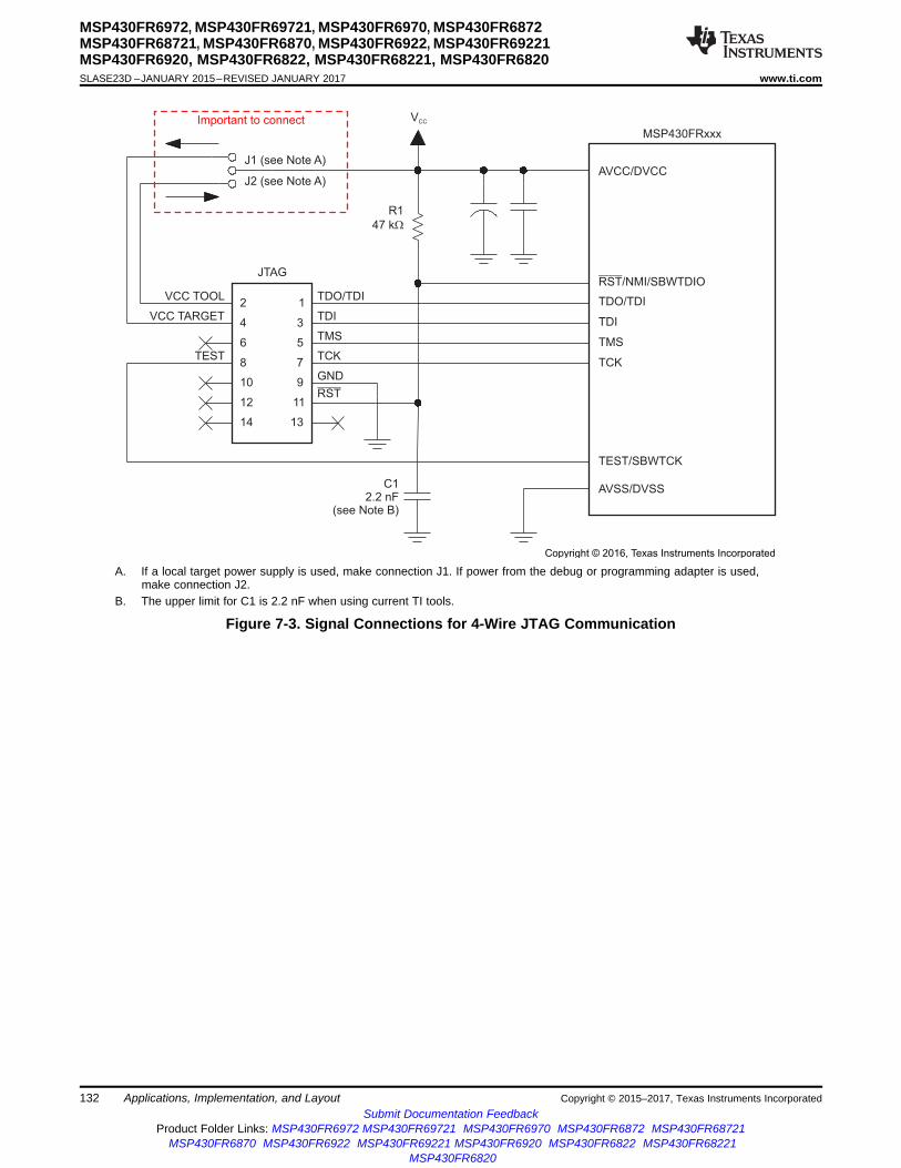
1
3
5
7
9
11
13
2
4
6
8
10
12
14
TDO/TDI
TDI
TMS
TCK
GND
TEST
JTAG
VCC TOOL
VCC TARGET
J1 (see Note A)
J2 (see Note A)
VCC
R1
47 kW
AV /DVCCCC
RST/NMI/SBWTDIO
TDO/TDI
TDI
TMS
TCK
TEST/SBWTCK
AV /DVSS SS
MSP430FRxxx
C12.2 nF
(see Note B)
RST
Important to connect
Copyright © 2016, Texas Instruments Incorporated
132
MSP430FR6972, MSP430FR69721, MSP430FR6970, MSP430FR6872MSP430FR68721, MSP430FR6870, MSP430FR6922, MSP430FR69221MSP430FR6920, MSP430FR6822, MSP430FR68221, MSP430FR6820SLASE23D –JANUARY 2015–REVISED JANUARY 2017 www.ti.com
Submit Documentation FeedbackProduct Folder Links: MSP430FR6972 MSP430FR69721 MSP430FR6970 MSP430FR6872 MSP430FR68721
MSP430FR6870 MSP430FR6922 MSP430FR69221 MSP430FR6920 MSP430FR6822 MSP430FR68221MSP430FR6820
Applications, Implementation, and Layout Copyright © 2015–2017, Texas Instruments Incorporated
A. If a local target power supply is used, make connection J1. If power from the debug or programming adapter is used,make connection J2.
B. The upper limit for C1 is 2.2 nF when using current TI tools.
Figure 7-3. Signal Connections for 4-Wire JTAG Communication

1
3
5
7
9
11
13
2
4
6
8
10
12
14
TEST/SBWTCK
MSP430FRxxx
RST/NMI/SBWTDIOTDO/TDI
TCK
GND
JTAG
R147 kΩ
(See Note B)
VCC TOOL
VCC TARGET
C12.2 nF
(See Note B)
J1 (see Note A)
J2 (see Note A)
Important to connect
AV /DVCCCC
AV /DVSS SS
VCC
Copyright © 2016, Texas Instruments Incorporated
133
MSP430FR6972, MSP430FR69721, MSP430FR6970, MSP430FR6872MSP430FR68721, MSP430FR6870, MSP430FR6922, MSP430FR69221MSP430FR6920, MSP430FR6822, MSP430FR68221, MSP430FR6820
www.ti.com SLASE23D –JANUARY 2015–REVISED JANUARY 2017
Submit Documentation FeedbackProduct Folder Links: MSP430FR6972 MSP430FR69721 MSP430FR6970 MSP430FR6872 MSP430FR68721
MSP430FR6870 MSP430FR6922 MSP430FR69221 MSP430FR6920 MSP430FR6822 MSP430FR68221MSP430FR6820
Applications, Implementation, and LayoutCopyright © 2015–2017, Texas Instruments Incorporated
A. Make connection J1 if a local target power supply is used, or make connection J2 if the target is powered from thedebug or programming adapter.
B. The device RST/NMI/SBWTDIO pin is used in 2-wire mode for bidirectional communication with the device duringJTAG access, and any capacitance that is attached to this signal may affect the ability to establish a connection withthe device. The upper limit for C1 is 2.2 nF when using current TI tools.
Figure 7-4. Signal Connections for 2-Wire JTAG Communication (Spy-Bi-Wire)
7.1.4 ResetThe reset pin can be configured as a reset function (default) or as an NMI function in the special functionregister (SFR) SFRRPCR.
In reset mode, the RST/NMI pin is active low, and a pulse applied to this pin that meets the reset timingspecifications generates a BOR-type device reset.
Setting SYSNMI causes the RST/NMI pin to be configured as an external NMI source. The external NMI isedge sensitive, and its edge is selectable by SYSNMIIES. Setting the NMIIE enables the interrupt of theexternal NMI. When an external NMI event occurs, the NMIIFG is set.
The RST/NMI pin can have either a pullup or pulldown that is enabled or not. SYSRSTUP selects eitherpullup or pulldown, and SYSRSTRE causes the pullup (default) or pulldown to be enabled (default) or not.If the RST/NMI pin is unused, it is required either to select and enable the internal pullup or to connect anexternal 47-kΩ pullup resistor to the RST/NMI pin with a 10-nF pulldown capacitor. The pulldown capacitorshould not exceed 2.2 nF when using devices with Spy-Bi-Wire interface in Spy-Bi-Wire mode or in 4-wireJTAG mode with TI tools like FET interfaces or GANG programmers.
See the MSP430FR58xx, MSP430FR59xx, MSP430FR68xx, and MSP430FR69xx Family User's Guide formore information on the referenced control registers and bits.
7.1.5 Unused PinsFor details on the connection of unused pins, see Section 4.6.

Using anExternalPositiveReference
Using anExternalNegativeReference
VEREF-
VREF+/VEREF+
+
+
4.7 µF10 Fµ
4.7 µF10 Fµ
AVSS
134
MSP430FR6972, MSP430FR69721, MSP430FR6970, MSP430FR6872MSP430FR68721, MSP430FR6870, MSP430FR6922, MSP430FR69221MSP430FR6920, MSP430FR6822, MSP430FR68221, MSP430FR6820SLASE23D –JANUARY 2015–REVISED JANUARY 2017 www.ti.com
Submit Documentation FeedbackProduct Folder Links: MSP430FR6972 MSP430FR69721 MSP430FR6970 MSP430FR6872 MSP430FR68721
MSP430FR6870 MSP430FR6922 MSP430FR69221 MSP430FR6920 MSP430FR6822 MSP430FR68221MSP430FR6820
Applications, Implementation, and Layout Copyright © 2015–2017, Texas Instruments Incorporated
7.1.6 General Layout Recommendations• Proper grounding and short traces for external crystal to reduce parasitic capacitance. See MSP430
32-kHz Crystal Oscillators for recommended layout guidelines.• Proper bypass capacitors on DVCC, AVCC, and reference pins if used.• Avoid routing any high-frequency signal close to an analog signal line. For example, keep digital
switching signals such as PWM or JTAG signals away from the oscillator circuit.• See Circuit Board Layout Techniques for a detailed discussion of PCB layout considerations. This
document is written primarily about op amps, but the guidelines are generally applicable for all mixed-signal applications.
• Proper ESD level protection should be considered to protect the device from unintended high-voltageelectrostatic discharge. See MSP430 System-Level ESD Considerations for guidelines.
7.1.7 Do's and Don'tsTI recommends powering AVCC and DVCC pins from the same source. At a minimum, during power up,power down, and device operation, the voltage difference between AVCC and DVCC must not exceed thelimits specified in the Absolute Maximum Ratings section. Exceeding the specified limits may causemalfunction of the device including erroneous writes to RAM and FRAM.
7.2 Peripheral- and Interface-Specific Design Information
7.2.1 ADC12_B Peripheral
7.2.1.1 Partial Schematic
Figure 7-5. ADC12_B Grounding and Noise Considerations
7.2.1.2 Design Requirements
As with any high-resolution ADC, appropriate printed-circuit-board layout and grounding techniques shouldbe followed to eliminate ground loops, unwanted parasitic effects, and noise.
Ground loops are formed when return current from the ADC flows through paths that are common withother analog or digital circuitry. If care is not taken, this current can generate small unwanted offsetvoltages that can add to or subtract from the reference or input voltages of the ADC. The generalguidelines in Section 7.1.1 combined with the connections shown in Section 7.2.1.1 prevent this.
In addition to grounding, ripple and noise spikes on the power-supply lines that are caused by digitalswitching or switching power supplies can corrupt the conversion result. TI recommends a noise-freedesign using separate analog and digital ground planes with a single-point connection to achieve highaccuracy.

135
MSP430FR6972, MSP430FR69721, MSP430FR6970, MSP430FR6872MSP430FR68721, MSP430FR6870, MSP430FR6922, MSP430FR69221MSP430FR6920, MSP430FR6822, MSP430FR68221, MSP430FR6820
www.ti.com SLASE23D –JANUARY 2015–REVISED JANUARY 2017
Submit Documentation FeedbackProduct Folder Links: MSP430FR6972 MSP430FR69721 MSP430FR6970 MSP430FR6872 MSP430FR68721
MSP430FR6870 MSP430FR6922 MSP430FR69221 MSP430FR6920 MSP430FR6822 MSP430FR68221MSP430FR6820
Applications, Implementation, and LayoutCopyright © 2015–2017, Texas Instruments Incorporated
Figure 7-5 shows the recommended decoupling circuit when an external voltage reference is used. Theinternal reference module has a maximum drive current as specified in the IO(VREF+) specification of theReference module.
The reference voltage must be a stable voltage for accurate measurements. The capacitor values that areselected in the general guidelines filter out the high- and low-frequency ripple before the reference voltageenters the device. In this case, the 10-µF capacitor is used to buffer the reference pin and filter any low-frequency ripple. A bypass capacitor of 4.7 µF is used to filter out any high-frequency noise.
7.2.1.3 Detailed Design Procedure
For additional design information, see Designing With the MSP430FR58xx, FR59xx, FR68xx, and FR69xxADC.
7.2.1.4 Layout Guidelines
Components that are shown in the partial schematic (see Figure 7-5) should be placed as close aspossible to the respective device pins. Avoid long traces, because they add additional parasiticcapacitance, inductance, and resistance on the signal.
Avoid routing analog input signals close to a high-frequency pin (for example, a high-frequency PWM),because the high-frequency switching can be coupled into the analog signal.
If differential mode is used for the ADC12_B, the analog differential input signals must be routed closetogether to minimize the effect of noise on the resulting signal.
7.2.2 LCD_C Peripheral
7.2.2.1 Partial Schematic
Required LCD connections greatly vary by the type of display that is used (static or multiplexed), whetherexternal or internal biasing is used, and whether the on-chip charge pump is employed. Also, there is afair amount of flexibility as to how the segment (Sx) and common (COMx) signals are connected to theMCU which can provide unique benefits. Because LCD connections are application specific, it is difficult toprovide a single one-fits-all schematic. However, for examples and how-to circuit design guidance, seeDesigning With MSP430™ MCUs and Segment LCDs.
7.2.2.2 Design Requirements
Due to the flexibility of the LCD_C peripheral module to accommodate various segment-based LCDs,selecting the correct display for the application in combination with determining specific designrequirements is often an iterative process. TI strongly recommends reviewing the LCD_C peripheralmodule chapter in the MSP430FR58xx, MSP430FR59xx, MSP430FR68xx, and MSP430FR69xx FamilyUser's Guide and Designing With MSP430™ MCUs and Segment LCDs during the initial designrequirements and decision process.
7.2.2.3 Detailed Design Procedure
A major component in designing the LCD solution is determining the exact connections between theLCD_C peripheral module and the display itself. One of the following basic design processes can beemployed for this step, although a balanced co-design approach is often recommended:• PCB layout-driven design that optimizes signal routing• Software-driven design that optimizes computational overhead
For a detailed discussion of the design procedure as well as for design information regarding the LCDcontroller input voltage selection including internal and external options, contrast control, and biasgeneration, see Designing With MSP430™ MCUs and Segment LCDs and the LCD_C controller chapterin the MSP430FR58xx, MSP430FR59xx, MSP430FR68xx, and MSP430FR69xx Family User's Guide.
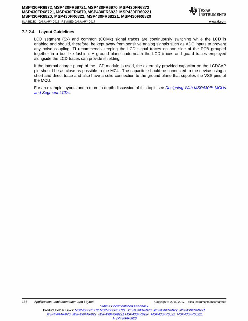
136
MSP430FR6972, MSP430FR69721, MSP430FR6970, MSP430FR6872MSP430FR68721, MSP430FR6870, MSP430FR6922, MSP430FR69221MSP430FR6920, MSP430FR6822, MSP430FR68221, MSP430FR6820SLASE23D –JANUARY 2015–REVISED JANUARY 2017 www.ti.com
Submit Documentation FeedbackProduct Folder Links: MSP430FR6972 MSP430FR69721 MSP430FR6970 MSP430FR6872 MSP430FR68721
MSP430FR6870 MSP430FR6922 MSP430FR69221 MSP430FR6920 MSP430FR6822 MSP430FR68221MSP430FR6820
Applications, Implementation, and Layout Copyright © 2015–2017, Texas Instruments Incorporated
7.2.2.4 Layout Guidelines
LCD segment (Sx) and common (COMx) signal traces are continuously switching while the LCD isenabled and should, therefore, be kept away from sensitive analog signals such as ADC inputs to preventany noise coupling. TI recommends keeping the LCD signal traces on one side of the PCB groupedtogether in a bus-like fashion. A ground plane underneath the LCD traces and guard traces employedalongside the LCD traces can provide shielding.
If the internal charge pump of the LCD module is used, the externally provided capacitor on the LCDCAPpin should be as close as possible to the MCU. The capacitor should be connected to the device using ashort and direct trace and also have a solid connection to the ground plane that supplies the VSS pins ofthe MCU.
For an example layouts and a more in-depth discussion of this topic see Designing With MSP430™ MCUsand Segment LCDs.

137
MSP430FR6972, MSP430FR69721, MSP430FR6970, MSP430FR6872MSP430FR68721, MSP430FR6870, MSP430FR6922, MSP430FR69221MSP430FR6920, MSP430FR6822, MSP430FR68221, MSP430FR6820
www.ti.com SLASE23D –JANUARY 2015–REVISED JANUARY 2017
Submit Documentation FeedbackProduct Folder Links: MSP430FR6972 MSP430FR69721 MSP430FR6970 MSP430FR6872 MSP430FR68721
MSP430FR6870 MSP430FR6922 MSP430FR69221 MSP430FR6920 MSP430FR6822 MSP430FR68221MSP430FR6820
Device and Documentation SupportCopyright © 2015–2017, Texas Instruments Incorporated
8 Device and Documentation Support
8.1 Getting Started and Next StepsFor more information on the MSP430™ family of devices and the tools and libraries that are available tohelp with your development, visit the Getting Started page.
8.2 Device NomenclatureTo designate the stages in the product development cycle, TI assigns prefixes to the part numbers of allMSP430 MCU devices and support tools. Each MSP430 MCU commercial family member has one ofthree prefixes: MSP, PMS, or XMS (for example, MSP430FR59721). TI recommends two of three possibleprefix designators for its support tools: MSP and MSPX. These prefixes represent evolutionary stages ofproduct development from engineering prototypes (with XMS for devices and MSPX for tools) through fullyqualified production devices and tools (with MSP for devices and MSP for tools).
Device development evolutionary flow:
XMS – Experimental device that is not necessarily representative of the electrical specifications for thefinal device
MSP – Fully qualified production device
Support tool development evolutionary flow:
MSPX – Development-support product that has not yet completed TI's internal qualification testing.
MSP – Fully-qualified development-support product
XMS devices and MSPX development-support tools are shipped against the following disclaimer:
"Developmental product is intended for internal evaluation purposes."
MSP devices and MSP development-support tools have been characterized fully, and the quality andreliability of the device have been demonstrated fully. TI's standard warranty applies.
Predictions show that prototype devices (XMS) have a greater failure rate than the standard productiondevices. TI recommends that these devices not be used in any production system because their expectedend-use failure rate still is undefined. Only qualified production devices are to be used.
TI device nomenclature also includes a suffix with the device family name. This suffix indicates thepackage type (for example, RGC) and temperature range (for example, T). Figure 8-1 provides a legendfor reading the complete device name for any family member.

Feature Set
Series
Processor Family
Optional: Temperature Range
MCU Platform
Device Type
Optional: Distribution Format
Packaging
MSP 430 FR 6 9721 I RGC T
Optional: BSL
FRAM
AES
Oscillators
ProcessorFamily
MSP = Mixed Signal ProcessorXMS = Experimental Silicon
MCUPlatform
TI’s 16-bit Low-Power Microcontroller PlatformMSP430
DeviceType
Memory TypeFR = FRAM
Series FRAM 6 Series = Up to 16 MHz with LCDFRAM 5 Series = Up to 16 MHz without LCD
FeatureSet
AES9 = AES8 = No AES
Oscillators7 = HFXT and LFXT2 = LFXT
FRAM (KB)2 = 640 = 32
Optional - BSL1 = I CNo value = UART
2
Optional:TemperatureRange
Packaging http://www.ti.com/packaging
Optional:DistributionFormat
Optional:AdditionalFeatures
-Q1 =-EP = Enhanced Product (–40°C to 105°C)-HT = Extreme Temperature Parts (–55°C to 150°C)
Automotive Qualified
T = Small ReelR = Large ReelNo Markings = Tube or Tray
S = 0°C to 50 CI = –40 C to 85 CT = –40 C to 105 C
°° °° °
138
MSP430FR6972, MSP430FR69721, MSP430FR6970, MSP430FR6872MSP430FR68721, MSP430FR6870, MSP430FR6922, MSP430FR69221MSP430FR6920, MSP430FR6822, MSP430FR68221, MSP430FR6820SLASE23D –JANUARY 2015–REVISED JANUARY 2017 www.ti.com
Submit Documentation FeedbackProduct Folder Links: MSP430FR6972 MSP430FR69721 MSP430FR6970 MSP430FR6872 MSP430FR68721
MSP430FR6870 MSP430FR6922 MSP430FR69221 MSP430FR6920 MSP430FR6822 MSP430FR68221MSP430FR6820
Device and Documentation Support Copyright © 2015–2017, Texas Instruments Incorporated
Figure 8-1. Device Nomenclature

139
MSP430FR6972, MSP430FR69721, MSP430FR6970, MSP430FR6872MSP430FR68721, MSP430FR6870, MSP430FR6922, MSP430FR69221MSP430FR6920, MSP430FR6822, MSP430FR68221, MSP430FR6820
www.ti.com SLASE23D –JANUARY 2015–REVISED JANUARY 2017
Submit Documentation FeedbackProduct Folder Links: MSP430FR6972 MSP430FR69721 MSP430FR6970 MSP430FR6872 MSP430FR68721
MSP430FR6870 MSP430FR6922 MSP430FR69221 MSP430FR6920 MSP430FR6822 MSP430FR68221MSP430FR6820
Device and Documentation SupportCopyright © 2015–2017, Texas Instruments Incorporated
8.3 Tools and SoftwareAll MSP microcontrollers are supported by a wide variety of software and hardware development tools.Tools are available from TI and various third parties. See them all at Development Kits and Software forLow-Power MCUs.
Table 8-1 lists the debug features of the MSP430FR697x(1), MSP430FR687x(1), MSP430FR692x(1), andMSP430FR682x(1) MCUs. See the Code Composer Studio for MSP430 User's Guide for details on theavailable features.
Table 8-1. Hardware Debug Features
MSP430ARCHITECTURE
4-WIREJTAG
2-WIREJTAG
BREAK-POINTS
RANGEBREAK-POINTS
CLOCKCONTROL
STATESEQUENCER
TRACEBUFFER
LPMx.5DEBUGGING
SUPPORTEnergyTrace++TECHNOLOGY
MSP430Xv2 Yes Yes 3 Yes Yes No No Yes Yes
Design Kits and Evaluation ModulesMSP430FR6989 LaunchPad Development Kit The MSP-EXP430FR6989 LaunchPad Development Kit
is an easy-to-use Evaluation Module (EVM) for the MSP40FR6989 microcontroller (MCU). Itcontains everything needed to start developing on the ultra-low-power MSP430FRx FRAMmicrocontroller platform, including onboard emulation for programming, debugging, andenergy measurements.
MSP-TS430PM64F - MSP430 64-pin FRAM Target Socket Board The MSP-TS430PZ5X100 is a stand-alone ZIF socket target board used to program and debug the MSP430 MCU in-systemthrough the JTAG interface or the Spy-Bi-Wire (2-wire JTAG) protocol.
MSP-FET430U64F - MSP430 64-pin FRAM TS Board and MSP-FET Bundle The MSP-FET430U64F isa bundle containing the MSP-FET emulator and a stand-alone 64-pin ZIF socket targetboard to program and debug the MSP430 in-system through the JTAG interface or the Spy-Bi-Wire (2-wire JTAG) protocol. The TS development board supports the MSP430FR6972FRAM device in a 64-pin LQFP package (TI package code: PM).
SoftwareMSP430Ware™ Software MSP430Ware software is a collection of code examples, data sheets, and
other design resources for all MSP430 devices delivered in a convenient package. Inaddition to providing a complete collection of existing MSP430 MCU design resources,MSP430Ware software also includes a high-level API called MSP Driver Library. This librarymakes it easy to program MSP430 hardware. MSP430Ware software is available as acomponent of CCS or as a stand-alone package.
MSP430FR592x, MSP430FR5x7x, MSP430FR6x2x, MSP430FR6x7x Code Examples C Codeexamples are available for every MSP device that configures each of the integratedperipherals for various application needs.
Capacitive Touch Software Library Free C libraries for enabling capacitive touch capabilities onMSP430 MCUs. The MSP430 MCU version of the library features several capacitive touchimplementations including the RO and RC method.
MSP Driver Library The abstracted API of MSP Driver Library provides easy-to-use function calls thatfree you from directly manipulating the bits and bytes of the MSP430 hardware. Thoroughdocumentation is delivered through a helpful API Guide, which includes details on eachfunction call and the recognized parameters. Developers can use Driver Library functions towrite complete projects with minimal overhead.
MSP EnergyTrace™ Technology EnergyTrace technology for MSP430 microcontrollers is an energy-based code analysis tool that measures and displays the energy profile of the applicationand helps to optimize it for ultra-low-power consumption.
ULP (Ultra-Low Power) Advisor ULP Advisor™ software is a tool for guiding developers to write moreefficient code to fully use the unique ultra-low-power features of MSP and MSP432microcontrollers. Aimed at both experienced and new microcontroller developers, ULPAdvisor checks your code against a thorough ULP checklist to help minimize the energyconsumption of your application. At build time, ULP Advisor provides notifications andremarks to identify areas of your code that can be further optimized for lower power.

140
MSP430FR6972, MSP430FR69721, MSP430FR6970, MSP430FR6872MSP430FR68721, MSP430FR6870, MSP430FR6922, MSP430FR69221MSP430FR6920, MSP430FR6822, MSP430FR68221, MSP430FR6820SLASE23D –JANUARY 2015–REVISED JANUARY 2017 www.ti.com
Submit Documentation FeedbackProduct Folder Links: MSP430FR6972 MSP430FR69721 MSP430FR6970 MSP430FR6872 MSP430FR68721
MSP430FR6870 MSP430FR6922 MSP430FR69221 MSP430FR6920 MSP430FR6822 MSP430FR68221MSP430FR6820
Device and Documentation Support Copyright © 2015–2017, Texas Instruments Incorporated
IEC60730 Software Package The IEC60730 MSP430 software package was developed to helpcustomers comply with IEC 60730-1:2010 (Automatic Electrical Controls for Household andSimilar Use – Part 1: General Requirements) for up to Class B products, which includeshome appliances, arc detectors, power converters, power tools, e-bikes, and many others.The IEC60730 MSP430 software package can be embedded in customer applicationsrunning on MSP430s to help simplify the customer’s certification efforts of functional safety-compliant consumer devices to IEC 60730-1:2010 Class B.
Fixed Point Math Library for MSP The MSP IQmath and Qmath Libraries are a collection of highlyoptimized and high-precision mathematical functions for C programmers to seamlessly port afloating-point algorithm into fixed-point code on MSP430 and MSP432 devices. Theseroutines are typically used in computationally intensive real-time applications where optimalexecution speed, high accuracy, and ultra-low energy are critical. By using the IQmath andQmath libraries, it is possible to achieve execution speeds considerably faster and energyconsumption considerably lower than equivalent code written using floating-point math.
Floating Point Math Library for MSP430 Continuing to innovate in the low-power and low-costmicrocontroller space, TI provides MSPMATHLIB. Leveraging the intelligent peripherals ofMSP devices, this floating-point math library of scalar functions is up to 26 times faster thanthe standard MSP430 math functions. Mathlib is easy to integrate into your designs. Thislibrary is free and is integrated in both Code Composer Studio IDE and IAR EmbeddedWorkbench IDE.
Development ToolsCode Composer Studio™ Integrated Development Environment for MSP Microcontrollers Code
Composer Studio (CCS) integrated development environment (IDE) supports all MSPmicrocontroller devices. CCS comprises a suite of embedded software utilities used todevelop and debug embedded applications. CCS includes an optimizing C/C++ compiler,source code editor, project build environment, debugger, profiler, and many other features.
Command-Line Programmer MSP Flasher is an open-source shell-based interface for programmingMSP microcontrollers through a FET programmer or eZ430 using JTAG or Spy-Bi-Wire(SBW) communication. MSP Flasher can download binary files (.txt or .hex) directly to theMSP microcontroller without an IDE.
MSP MCU Programmer and Debugger The MSP-FET is a powerful emulation development tool – oftencalled a debug probe – which lets users quickly begin application development on MSP low-power MCUs. Creating MCU software usually requires downloading the resulting binaryprogram to the MSP device for validation and debugging.
MSP-GANG Production Programmer The MSP Gang Programmer is an MSP430 or MSP432 deviceprogrammer that can program up to eight identical MSP430 or MSP432 flash or FRAMdevices at the same time. The MSP Gang Programmer connects to a host PC using astandard RS-232 or USB connection and provides flexible programming options that let theuser fully customize the process.

141
MSP430FR6972, MSP430FR69721, MSP430FR6970, MSP430FR6872MSP430FR68721, MSP430FR6870, MSP430FR6922, MSP430FR69221MSP430FR6920, MSP430FR6822, MSP430FR68221, MSP430FR6820
www.ti.com SLASE23D –JANUARY 2015–REVISED JANUARY 2017
Submit Documentation FeedbackProduct Folder Links: MSP430FR6972 MSP430FR69721 MSP430FR6970 MSP430FR6872 MSP430FR68721
MSP430FR6870 MSP430FR6922 MSP430FR69221 MSP430FR6920 MSP430FR6822 MSP430FR68221MSP430FR6820
Device and Documentation SupportCopyright © 2015–2017, Texas Instruments Incorporated
8.4 Documentation SupportThe following documents describe the MSP430FR697x(1), MSP430FR687x(1), MSP430FR692x(1), andMSP430FR682x(1) MCUs. Copies of these documents are available on the Internet at www.ti.com.
Receiving Notification of Document Updates
To receive notification of documentation updates—including silicon errata—go to the product folder foryour device on ti.com (for links to product folders, see Section 8.5). In the upper right corner, click the"Alert me" button. This registers you to receive a weekly digest of product information that has changed (ifany). For change details, check the revision history of any revised document.
ErrataMSP430FR6972 Device Erratasheet Describes the known exceptions to the functional specifications.MSP430FR69721 Device Erratasheet Describes the known exceptions to the functional specifications.MSP430FR6970 Device Erratasheet Describes the known exceptions to the functional specifications.MSP430FR6922 Device Erratasheet Describes the known exceptions to the functional specifications.MSP430FR69221 Device Erratasheet Describes the known exceptions to the functional specifications.MSP430FR6920 Device Erratasheet Describes the known exceptions to the functional specifications.MSP430FR6872 Device Erratasheet Describes the known exceptions to the functional specifications.MSP430FR68721 Device Erratasheet Describes the known exceptions to the functional specifications.MSP430FR6870 Device Erratasheet Describes the known exceptions to the functional specifications.MSP430FR6822 Device Erratasheet Describes the known exceptions to the functional specifications.MSP430FR68221 Device Erratasheet Describes the known exceptions to the functional specifications.MSP430FR6820 Device Erratasheet Describes the known exceptions to the functional specifications.
User's GuidesMSP430FR58xx, MSP430FR59xx, MSP430FR68xx, and MSP430FR69xx Family User's Guide
Detailed information on the modules and peripherals available in this device family.MSP430FR57xx, MSP430FR58xx, MSP430FR59xx, MSP430FR68xx, and MSP430FR69xx Bootloader
(BSL)The bootloader (BSL, formerly known as the bootstrap loader) provides a method to programmemory during MSP430 MCU project development and updates. It can be activated by autility that sends commands using a serial protocol. The BSL lets the user control the activityof the MSP430 and to exchange data using a personal computer or other device.
MSP430 Programming With the JTAG Interface This document describes the functions that arerequired to erase, program, and verify the memory module of the MSP430 flash-based andFRAM-based microcontroller families using the JTAG communication port. In addition, itdescribes how to program the JTAG access security fuse that is available on all MSP430devices. This document describes device access using both the standard 4-wire JTAGinterface and the 2-wire JTAG interface, which is also referred to as Spy-Bi-Wire (SBW).
MSP430 Hardware Tools User's Guide This manual describes the hardware of the TI MSP-FET430Flash Emulation Tool (FET). The FET is the program development tool for the MSP430 ultra-low-power microcontroller. Both available interface types, the parallel port interface and theUSB interface, are described.
Application ReportsDesigning With MSP430 and Segment LCDs Segment liquid crystal displays (LCDs) are needed to
provide information to users in a wide variety of applications from smart meters to electronicshelf labels (ESLs) to medical equipment. Several MSP430™ microcontroller families includebuilt-in low-power LCD driver circuitry that allows the MSP430 MCU to directly control thesegmented LCD glass. This application note helps explain how segmented LCDs work, thedifferent features of the various LCD modules across the MSP430 MCU family, LCDhardware layout tips, guidance on writing efficient and easy-to-use LCD driver software, andan overview of the portfolio of MSP430 devices that include different LCD features to aid indevice selection.

142
MSP430FR6972, MSP430FR69721, MSP430FR6970, MSP430FR6872MSP430FR68721, MSP430FR6870, MSP430FR6922, MSP430FR69221MSP430FR6920, MSP430FR6822, MSP430FR68221, MSP430FR6820SLASE23D –JANUARY 2015–REVISED JANUARY 2017 www.ti.com
Submit Documentation FeedbackProduct Folder Links: MSP430FR6972 MSP430FR69721 MSP430FR6970 MSP430FR6872 MSP430FR68721
MSP430FR6870 MSP430FR6922 MSP430FR69221 MSP430FR6920 MSP430FR6822 MSP430FR68221MSP430FR6820
Device and Documentation Support Copyright © 2015–2017, Texas Instruments Incorporated
MSP430 FRAM Technology – How-To and Best Practices FRAM is a nonvolatile memory technologythat behaves like SRAM while enabling a whole host of new applications, but also changesthe way firmware should be designed. This application report outlines the how-to and bestpractices of using FRAM technology in MSP430 from an embedded software developmentperspective. It discusses how to implement a memory layout according to application-specificcode, constant, data space requirements, the use of FRAM to optimize application energyconsumption, and the use of the Memory Protection Unit (MPU) to maximize applicationrobustness by protecting the program code against unintended write accesses.
MSP430 32-kHz Crystal Oscillators Selection of the correct crystal, correct load circuit, and properboard layout are important for a stable crystal oscillator. This application report summarizescrystal oscillator function and explains the parameters to select the correct crystal forMSP430 ultra-low-power operation. In addition, hints and examples for correct board layoutare given. The document also contains detailed information on the possible oscillator tests toensure stable oscillator operation in mass production.
MSP430 System-Level ESD Considerations System-Level ESD has become increasingly demandingwith silicon technology scaling towards lower voltages and the need for designing cost-effective and ultra-low-power components. This application report addresses three differentESD topics to help board designers and OEMs understand and design robust system-leveldesigns.
8.5 Related LinksTable 8-2 lists quick access links. Categories include technical documents, support and communityresources, tools and software, and quick access to sample or buy.
Table 8-2. Related Links
PARTS PRODUCT FOLDER ORDER NOW TECHNICALDOCUMENTS
TOOLS &SOFTWARE
SUPPORT &COMMUNITY
MSP430FR6972 Click here Click here Click here Click here Click hereMSP430FR69721 Click here Click here Click here Click here Click hereMSP430FR6970 Click here Click here Click here Click here Click hereMSP430FR6872 Click here Click here Click here Click here Click hereMSP430FR68721 Click here Click here Click here Click here Click hereMSP430FR6870 Click here Click here Click here Click here Click hereMSP430FR6922 Click here Click here Click here Click here Click hereMSP430FR69221 Click here Click here Click here Click here Click hereMSP430FR6920 Click here Click here Click here Click here Click hereMSP430FR6822 Click here Click here Click here Click here Click hereMSP430FR68221 Click here Click here Click here Click here Click hereMSP430FR6820 Click here Click here Click here Click here Click here
8.6 Community ResourcesThe following links connect to TI community resources. Linked contents are provided "AS IS" by therespective contributors. They do not constitute TI specifications and do not necessarily reflect TI's views;see TI's Terms of Use.
TI E2E™ CommunityTI's Engineer-to-Engineer (E2E) Community. Created to foster collaboration among engineers. Ate2e.ti.com, you can ask questions, share knowledge, explore ideas, and help solve problems with fellowengineers.
TI Embedded Processors WikiTexas Instruments Embedded Processors Wiki. Established to help developers get started with embeddedprocessors from Texas Instruments and to foster innovation and growth of general knowledge about thehardware and software surrounding these devices.

143
MSP430FR6972, MSP430FR69721, MSP430FR6970, MSP430FR6872MSP430FR68721, MSP430FR6870, MSP430FR6922, MSP430FR69221MSP430FR6920, MSP430FR6822, MSP430FR68221, MSP430FR6820
www.ti.com SLASE23D –JANUARY 2015–REVISED JANUARY 2017
Submit Documentation FeedbackProduct Folder Links: MSP430FR6972 MSP430FR69721 MSP430FR6970 MSP430FR6872 MSP430FR68721
MSP430FR6870 MSP430FR6922 MSP430FR69221 MSP430FR6920 MSP430FR6822 MSP430FR68221MSP430FR6820
Device and Documentation SupportCopyright © 2015–2017, Texas Instruments Incorporated
8.7 TrademarksEnergyTrace++, MSP430, MSP430Ware, EnergyTrace, ULP Advisor, Code Composer Studio, E2E aretrademarks of Texas Instruments.Microsoft is a registered trademark of Microsoft Corporation.All other trademarks are the property of their respective owners.
8.8 Electrostatic Discharge CautionThis integrated circuit can be damaged by ESD. Texas Instruments recommends that all integrated circuits be handled withappropriate precautions. Failure to observe proper handling and installation procedures can cause damage.
ESD damage can range from subtle performance degradation to complete device failure. Precision integrated circuits may be moresusceptible to damage because very small parametric changes could cause the device not to meet its published specifications.
8.9 Export Control NoticeRecipient agrees to not knowingly export or re-export, directly or indirectly, any product or technical data(as defined by the U.S., EU, and other Export Administration Regulations) including software, or anycontrolled product restricted by other applicable national regulations, received from disclosing party undernondisclosure obligations (if any), or any direct product of such technology, to any destination to whichsuch export or re-export is restricted or prohibited by U.S. or other applicable laws, without obtaining priorauthorization from U.S. Department of Commerce and other competent Government authorities to theextent required by those laws.
8.10 GlossaryTI Glossary This glossary lists and explains terms, acronyms, and definitions.

144
MSP430FR6972, MSP430FR69721, MSP430FR6970, MSP430FR6872MSP430FR68721, MSP430FR6870, MSP430FR6922, MSP430FR69221MSP430FR6920, MSP430FR6822, MSP430FR68221, MSP430FR6820SLASE23D –JANUARY 2015–REVISED JANUARY 2017 www.ti.com
Submit Documentation FeedbackProduct Folder Links: MSP430FR6972 MSP430FR69721 MSP430FR6970 MSP430FR6872 MSP430FR68721
MSP430FR6870 MSP430FR6922 MSP430FR69221 MSP430FR6920 MSP430FR6822 MSP430FR68221MSP430FR6820
Mechanical, Packaging, and Orderable Information Copyright © 2015–2017, Texas Instruments Incorporated
9 Mechanical, Packaging, and Orderable Information
The following pages include mechanical, packaging, and orderable information. This information is themost current data available for the designated devices. This data is subject to change without notice andrevision of this document. For browser-based versions of this data sheet, refer to the left-hand navigation.
PACKAGE OPTION ADDENDUM
www.ti.com 23-Jul-2015
Addendum-Page 1
PACKAGING INFORMATION
Orderable Device Status(1)
Package Type PackageDrawing
Pins PackageQty
Eco Plan(2)
Lead/Ball Finish(6)
MSL Peak Temp(3)
Op Temp (°C) Device Marking(4/5)
Samples
MSP430FR6820IG56R ACTIVE TSSOP DGG 56 2000 Green (RoHS& no Sb/Br)
CU NIPDAU Level-3-260C-168 HR -40 to 85 FR6820
MSP430FR6820IPMR ACTIVE LQFP PM 64 1000 Green (RoHS& no Sb/Br)
CU NIPDAU Level-3-260C-168 HR -40 to 85 FR6820
MSP430FR6820IRGCR ACTIVE VQFN RGC 64 2000 Green (RoHS& no Sb/Br)
CU NIPDAU Level-3-260C-168 HR -40 to 85 FR6820
MSP430FR68221IG56R ACTIVE TSSOP DGG 56 2000 Green (RoHS& no Sb/Br)
CU NIPDAU Level-3-260C-168 HR -40 to 85 FR68221
MSP430FR68221IPMR ACTIVE LQFP PM 64 1000 Green (RoHS& no Sb/Br)
CU NIPDAU Level-3-260C-168 HR -40 to 85 FR68221
MSP430FR68221IRGCR ACTIVE VQFN RGC 64 2000 Green (RoHS& no Sb/Br)
CU NIPDAU Level-3-260C-168 HR -40 to 85 FR68221
MSP430FR6822IG56R ACTIVE TSSOP DGG 56 2000 Green (RoHS& no Sb/Br)
CU NIPDAU Level-3-260C-168 HR -40 to 85 FR6822
MSP430FR6822IPMR ACTIVE LQFP PM 64 1000 Green (RoHS& no Sb/Br)
CU NIPDAU Level-3-260C-168 HR -40 to 85 FR6822
MSP430FR6822IRGCR ACTIVE VQFN RGC 64 2000 Green (RoHS& no Sb/Br)
CU NIPDAU Level-3-260C-168 HR -40 to 85 FR6822
MSP430FR6870IPMR ACTIVE LQFP PM 64 1000 Green (RoHS& no Sb/Br)
CU NIPDAU Level-3-260C-168 HR -40 to 85 FR6870
MSP430FR6870IRGCR ACTIVE VQFN RGC 64 2000 Green (RoHS& no Sb/Br)
CU NIPDAU Level-3-260C-168 HR -40 to 85 FR6870
MSP430FR68721IPMR ACTIVE LQFP PM 64 1000 Green (RoHS& no Sb/Br)
CU NIPDAU Level-3-260C-168 HR -40 to 85 FR68721
MSP430FR68721IRGCR ACTIVE VQFN RGC 64 2000 Green (RoHS& no Sb/Br)
CU NIPDAU Level-3-260C-168 HR -40 to 85 FR68721
MSP430FR6872IPMR ACTIVE LQFP PM 64 1000 Green (RoHS& no Sb/Br)
CU NIPDAU Level-3-260C-168 HR -40 to 85 FR6872
MSP430FR6872IRGCR ACTIVE VQFN RGC 64 2000 Green (RoHS& no Sb/Br)
CU NIPDAU Level-3-260C-168 HR -40 to 85 FR6872
MSP430FR6920IG56R ACTIVE TSSOP DGG 56 2000 Green (RoHS& no Sb/Br)
CU NIPDAU Level-3-260C-168 HR -40 to 85 FR6920
MSP430FR6920IPMR ACTIVE LQFP PM 64 1000 Green (RoHS& no Sb/Br)
CU NIPDAU Level-3-260C-168 HR -40 to 85 FR6920
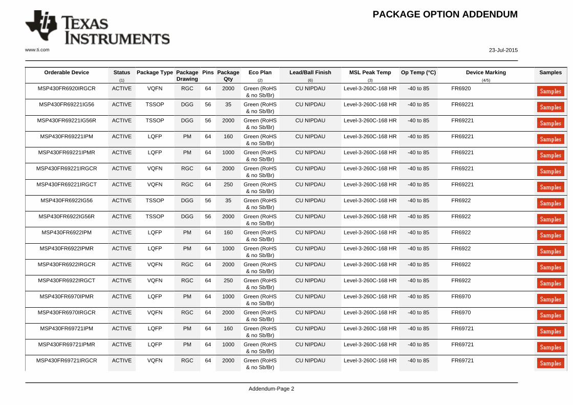
PACKAGE OPTION ADDENDUM
www.ti.com 23-Jul-2015
Addendum-Page 2
Orderable Device Status(1)
Package Type PackageDrawing
Pins PackageQty
Eco Plan(2)
Lead/Ball Finish(6)
MSL Peak Temp(3)
Op Temp (°C) Device Marking(4/5)
Samples
MSP430FR6920IRGCR ACTIVE VQFN RGC 64 2000 Green (RoHS& no Sb/Br)
CU NIPDAU Level-3-260C-168 HR -40 to 85 FR6920
MSP430FR69221IG56 ACTIVE TSSOP DGG 56 35 Green (RoHS& no Sb/Br)
CU NIPDAU Level-3-260C-168 HR -40 to 85 FR69221
MSP430FR69221IG56R ACTIVE TSSOP DGG 56 2000 Green (RoHS& no Sb/Br)
CU NIPDAU Level-3-260C-168 HR -40 to 85 FR69221
MSP430FR69221IPM ACTIVE LQFP PM 64 160 Green (RoHS& no Sb/Br)
CU NIPDAU Level-3-260C-168 HR -40 to 85 FR69221
MSP430FR69221IPMR ACTIVE LQFP PM 64 1000 Green (RoHS& no Sb/Br)
CU NIPDAU Level-3-260C-168 HR -40 to 85 FR69221
MSP430FR69221IRGCR ACTIVE VQFN RGC 64 2000 Green (RoHS& no Sb/Br)
CU NIPDAU Level-3-260C-168 HR -40 to 85 FR69221
MSP430FR69221IRGCT ACTIVE VQFN RGC 64 250 Green (RoHS& no Sb/Br)
CU NIPDAU Level-3-260C-168 HR -40 to 85 FR69221
MSP430FR6922IG56 ACTIVE TSSOP DGG 56 35 Green (RoHS& no Sb/Br)
CU NIPDAU Level-3-260C-168 HR -40 to 85 FR6922
MSP430FR6922IG56R ACTIVE TSSOP DGG 56 2000 Green (RoHS& no Sb/Br)
CU NIPDAU Level-3-260C-168 HR -40 to 85 FR6922
MSP430FR6922IPM ACTIVE LQFP PM 64 160 Green (RoHS& no Sb/Br)
CU NIPDAU Level-3-260C-168 HR -40 to 85 FR6922
MSP430FR6922IPMR ACTIVE LQFP PM 64 1000 Green (RoHS& no Sb/Br)
CU NIPDAU Level-3-260C-168 HR -40 to 85 FR6922
MSP430FR6922IRGCR ACTIVE VQFN RGC 64 2000 Green (RoHS& no Sb/Br)
CU NIPDAU Level-3-260C-168 HR -40 to 85 FR6922
MSP430FR6922IRGCT ACTIVE VQFN RGC 64 250 Green (RoHS& no Sb/Br)
CU NIPDAU Level-3-260C-168 HR -40 to 85 FR6922
MSP430FR6970IPMR ACTIVE LQFP PM 64 1000 Green (RoHS& no Sb/Br)
CU NIPDAU Level-3-260C-168 HR -40 to 85 FR6970
MSP430FR6970IRGCR ACTIVE VQFN RGC 64 2000 Green (RoHS& no Sb/Br)
CU NIPDAU Level-3-260C-168 HR -40 to 85 FR6970
MSP430FR69721IPM ACTIVE LQFP PM 64 160 Green (RoHS& no Sb/Br)
CU NIPDAU Level-3-260C-168 HR -40 to 85 FR69721
MSP430FR69721IPMR ACTIVE LQFP PM 64 1000 Green (RoHS& no Sb/Br)
CU NIPDAU Level-3-260C-168 HR -40 to 85 FR69721
MSP430FR69721IRGCR ACTIVE VQFN RGC 64 2000 Green (RoHS& no Sb/Br)
CU NIPDAU Level-3-260C-168 HR -40 to 85 FR69721

PACKAGE OPTION ADDENDUM
www.ti.com 23-Jul-2015
Addendum-Page 3
Orderable Device Status(1)
Package Type PackageDrawing
Pins PackageQty
Eco Plan(2)
Lead/Ball Finish(6)
MSL Peak Temp(3)
Op Temp (°C) Device Marking(4/5)
Samples
MSP430FR69721IRGCT ACTIVE VQFN RGC 64 250 Green (RoHS& no Sb/Br)
CU NIPDAU Level-3-260C-168 HR -40 to 85 FR69721
MSP430FR6972IPM ACTIVE LQFP PM 64 160 Green (RoHS& no Sb/Br)
CU NIPDAU Level-3-260C-168 HR -40 to 85 FR6972
MSP430FR6972IPMR ACTIVE LQFP PM 64 1000 Green (RoHS& no Sb/Br)
CU NIPDAU Level-3-260C-168 HR -40 to 85 FR6972
MSP430FR6972IRGCR ACTIVE VQFN RGC 64 2000 Green (RoHS& no Sb/Br)
CU NIPDAU Level-3-260C-168 HR -40 to 85 FR6972
MSP430FR6972IRGCT ACTIVE VQFN RGC 64 250 Green (RoHS& no Sb/Br)
CU NIPDAU Level-3-260C-168 HR -40 to 85 FR6972
(1) The marketing status values are defined as follows:ACTIVE: Product device recommended for new designs.LIFEBUY: TI has announced that the device will be discontinued, and a lifetime-buy period is in effect.NRND: Not recommended for new designs. Device is in production to support existing customers, but TI does not recommend using this part in a new design.PREVIEW: Device has been announced but is not in production. Samples may or may not be available.OBSOLETE: TI has discontinued the production of the device.
(2) Eco Plan - The planned eco-friendly classification: Pb-Free (RoHS), Pb-Free (RoHS Exempt), or Green (RoHS & no Sb/Br) - please check http://www.ti.com/productcontent for the latest availabilityinformation and additional product content details.TBD: The Pb-Free/Green conversion plan has not been defined.Pb-Free (RoHS): TI's terms "Lead-Free" or "Pb-Free" mean semiconductor products that are compatible with the current RoHS requirements for all 6 substances, including the requirement thatlead not exceed 0.1% by weight in homogeneous materials. Where designed to be soldered at high temperatures, TI Pb-Free products are suitable for use in specified lead-free processes.Pb-Free (RoHS Exempt): This component has a RoHS exemption for either 1) lead-based flip-chip solder bumps used between the die and package, or 2) lead-based die adhesive used betweenthe die and leadframe. The component is otherwise considered Pb-Free (RoHS compatible) as defined above.Green (RoHS & no Sb/Br): TI defines "Green" to mean Pb-Free (RoHS compatible), and free of Bromine (Br) and Antimony (Sb) based flame retardants (Br or Sb do not exceed 0.1% by weightin homogeneous material)
(3) MSL, Peak Temp. - The Moisture Sensitivity Level rating according to the JEDEC industry standard classifications, and peak solder temperature.
(4) There may be additional marking, which relates to the logo, the lot trace code information, or the environmental category on the device.
(5) Multiple Device Markings will be inside parentheses. Only one Device Marking contained in parentheses and separated by a "~" will appear on a device. If a line is indented then it is a continuationof the previous line and the two combined represent the entire Device Marking for that device.
(6) Lead/Ball Finish - Orderable Devices may have multiple material finish options. Finish options are separated by a vertical ruled line. Lead/Ball Finish values may wrap to two lines if the finishvalue exceeds the maximum column width.

PACKAGE OPTION ADDENDUM
www.ti.com 23-Jul-2015
Addendum-Page 4
Important Information and Disclaimer:The information provided on this page represents TI's knowledge and belief as of the date that it is provided. TI bases its knowledge and belief on informationprovided by third parties, and makes no representation or warranty as to the accuracy of such information. Efforts are underway to better integrate information from third parties. TI has taken andcontinues to take reasonable steps to provide representative and accurate information but may not have conducted destructive testing or chemical analysis on incoming materials and chemicals.TI and TI suppliers consider certain information to be proprietary, and thus CAS numbers and other limited information may not be available for release.
In no event shall TI's liability arising out of such information exceed the total purchase price of the TI part(s) at issue in this document sold by TI to Customer on an annual basis.
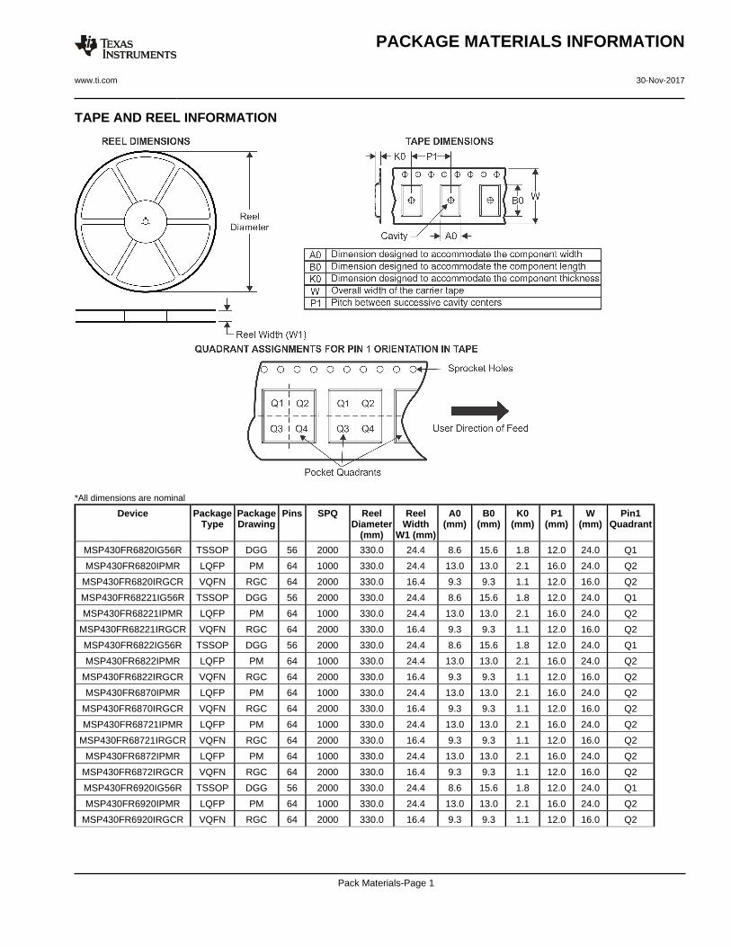
TAPE AND REEL INFORMATION
*All dimensions are nominal
Device PackageType
PackageDrawing
Pins SPQ ReelDiameter
(mm)
ReelWidth
W1 (mm)
A0(mm)
B0(mm)
K0(mm)
P1(mm)
W(mm)
Pin1Quadrant
MSP430FR6820IG56R TSSOP DGG 56 2000 330.0 24.4 8.6 15.6 1.8 12.0 24.0 Q1
MSP430FR6820IPMR LQFP PM 64 1000 330.0 24.4 13.0 13.0 2.1 16.0 24.0 Q2
MSP430FR6820IRGCR VQFN RGC 64 2000 330.0 16.4 9.3 9.3 1.1 12.0 16.0 Q2
MSP430FR68221IG56R TSSOP DGG 56 2000 330.0 24.4 8.6 15.6 1.8 12.0 24.0 Q1
MSP430FR68221IPMR LQFP PM 64 1000 330.0 24.4 13.0 13.0 2.1 16.0 24.0 Q2
MSP430FR68221IRGCR VQFN RGC 64 2000 330.0 16.4 9.3 9.3 1.1 12.0 16.0 Q2
MSP430FR6822IG56R TSSOP DGG 56 2000 330.0 24.4 8.6 15.6 1.8 12.0 24.0 Q1
MSP430FR6822IPMR LQFP PM 64 1000 330.0 24.4 13.0 13.0 2.1 16.0 24.0 Q2
MSP430FR6822IRGCR VQFN RGC 64 2000 330.0 16.4 9.3 9.3 1.1 12.0 16.0 Q2
MSP430FR6870IPMR LQFP PM 64 1000 330.0 24.4 13.0 13.0 2.1 16.0 24.0 Q2
MSP430FR6870IRGCR VQFN RGC 64 2000 330.0 16.4 9.3 9.3 1.1 12.0 16.0 Q2
MSP430FR68721IPMR LQFP PM 64 1000 330.0 24.4 13.0 13.0 2.1 16.0 24.0 Q2
MSP430FR68721IRGCR VQFN RGC 64 2000 330.0 16.4 9.3 9.3 1.1 12.0 16.0 Q2
MSP430FR6872IPMR LQFP PM 64 1000 330.0 24.4 13.0 13.0 2.1 16.0 24.0 Q2
MSP430FR6872IRGCR VQFN RGC 64 2000 330.0 16.4 9.3 9.3 1.1 12.0 16.0 Q2
MSP430FR6920IG56R TSSOP DGG 56 2000 330.0 24.4 8.6 15.6 1.8 12.0 24.0 Q1
MSP430FR6920IPMR LQFP PM 64 1000 330.0 24.4 13.0 13.0 2.1 16.0 24.0 Q2
MSP430FR6920IRGCR VQFN RGC 64 2000 330.0 16.4 9.3 9.3 1.1 12.0 16.0 Q2
PACKAGE MATERIALS INFORMATION
www.ti.com 30-Nov-2017
Pack Materials-Page 1

Device PackageType
PackageDrawing
Pins SPQ ReelDiameter
(mm)
ReelWidth
W1 (mm)
A0(mm)
B0(mm)
K0(mm)
P1(mm)
W(mm)
Pin1Quadrant
MSP430FR69221IG56R TSSOP DGG 56 2000 330.0 24.4 8.6 15.6 1.8 12.0 24.0 Q1
MSP430FR69221IPMR LQFP PM 64 1000 330.0 24.4 13.0 13.0 2.1 16.0 24.0 Q2
MSP430FR69221IRGCR VQFN RGC 64 2000 330.0 16.4 9.3 9.3 1.1 12.0 16.0 Q2
MSP430FR69221IRGCT VQFN RGC 64 250 180.0 16.4 9.3 9.3 1.1 12.0 16.0 Q2
MSP430FR6922IG56R TSSOP DGG 56 2000 330.0 24.4 8.6 15.6 1.8 12.0 24.0 Q1
MSP430FR6922IPMR LQFP PM 64 1000 330.0 24.4 13.0 13.0 2.1 16.0 24.0 Q2
MSP430FR6922IRGCT VQFN RGC 64 250 180.0 16.4 9.3 9.3 1.1 12.0 16.0 Q2
MSP430FR6970IPMR LQFP PM 64 1000 330.0 24.4 13.0 13.0 2.1 16.0 24.0 Q2
MSP430FR6970IRGCR VQFN RGC 64 2000 330.0 16.4 9.3 9.3 1.1 12.0 16.0 Q2
MSP430FR69721IPMR LQFP PM 64 1000 330.0 24.4 13.0 13.0 2.1 16.0 24.0 Q2
MSP430FR69721IRGCR VQFN RGC 64 2000 330.0 16.4 9.3 9.3 1.1 12.0 16.0 Q2
MSP430FR69721IRGCT VQFN RGC 64 250 180.0 16.4 9.3 9.3 1.1 12.0 16.0 Q2
MSP430FR6972IPMR LQFP PM 64 1000 330.0 24.4 13.0 13.0 2.1 16.0 24.0 Q2
MSP430FR6972IRGCR VQFN RGC 64 2000 330.0 16.4 9.3 9.3 1.1 12.0 16.0 Q2
MSP430FR6972IRGCT VQFN RGC 64 250 180.0 16.4 9.3 9.3 1.1 12.0 16.0 Q2
*All dimensions are nominal
Device Package Type Package Drawing Pins SPQ Length (mm) Width (mm) Height (mm)
MSP430FR6820IG56R TSSOP DGG 56 2000 367.0 367.0 45.0
MSP430FR6820IPMR LQFP PM 64 1000 336.6 336.6 41.3
PACKAGE MATERIALS INFORMATION
www.ti.com 30-Nov-2017
Pack Materials-Page 2

Device Package Type Package Drawing Pins SPQ Length (mm) Width (mm) Height (mm)
MSP430FR6820IRGCR VQFN RGC 64 2000 367.0 367.0 38.0
MSP430FR68221IG56R TSSOP DGG 56 2000 367.0 367.0 45.0
MSP430FR68221IPMR LQFP PM 64 1000 336.6 336.6 41.3
MSP430FR68221IRGCR VQFN RGC 64 2000 367.0 367.0 38.0
MSP430FR6822IG56R TSSOP DGG 56 2000 367.0 367.0 45.0
MSP430FR6822IPMR LQFP PM 64 1000 336.6 336.6 41.3
MSP430FR6822IRGCR VQFN RGC 64 2000 367.0 367.0 38.0
MSP430FR6870IPMR LQFP PM 64 1000 336.6 336.6 41.3
MSP430FR6870IRGCR VQFN RGC 64 2000 367.0 367.0 38.0
MSP430FR68721IPMR LQFP PM 64 1000 336.6 336.6 41.3
MSP430FR68721IRGCR VQFN RGC 64 2000 367.0 367.0 38.0
MSP430FR6872IPMR LQFP PM 64 1000 336.6 336.6 41.3
MSP430FR6872IRGCR VQFN RGC 64 2000 367.0 367.0 38.0
MSP430FR6920IG56R TSSOP DGG 56 2000 367.0 367.0 45.0
MSP430FR6920IPMR LQFP PM 64 1000 336.6 336.6 41.3
MSP430FR6920IRGCR VQFN RGC 64 2000 367.0 367.0 38.0
MSP430FR69221IG56R TSSOP DGG 56 2000 367.0 367.0 45.0
MSP430FR69221IPMR LQFP PM 64 1000 336.6 336.6 41.3
MSP430FR69221IRGCR VQFN RGC 64 2000 367.0 367.0 38.0
MSP430FR69221IRGCT VQFN RGC 64 250 210.0 185.0 35.0
MSP430FR6922IG56R TSSOP DGG 56 2000 367.0 367.0 45.0
MSP430FR6922IPMR LQFP PM 64 1000 336.6 336.6 41.3
MSP430FR6922IRGCT VQFN RGC 64 250 210.0 185.0 35.0
MSP430FR6970IPMR LQFP PM 64 1000 336.6 336.6 41.3
MSP430FR6970IRGCR VQFN RGC 64 2000 367.0 367.0 38.0
MSP430FR69721IPMR LQFP PM 64 1000 336.6 336.6 41.3
MSP430FR69721IRGCR VQFN RGC 64 2000 367.0 367.0 38.0
MSP430FR69721IRGCT VQFN RGC 64 250 210.0 185.0 35.0
MSP430FR6972IPMR LQFP PM 64 1000 336.6 336.6 41.3
MSP430FR6972IRGCR VQFN RGC 64 2000 367.0 367.0 38.0
MSP430FR6972IRGCT VQFN RGC 64 250 210.0 185.0 35.0
PACKAGE MATERIALS INFORMATION
www.ti.com 30-Nov-2017
Pack Materials-Page 3

www.ti.com
PACKAGE OUTLINE
C
TYP8.37.9
1.2 MAX
54X 0.5
56X 0.270.17
2X13.5
(0.15) TYP
0 - 80.150.05
0.25GAGE PLANE
0.750.50
A
NOTE 3
14.113.9
B 6.26.0
4222167/A 07/2015
TSSOP - 1.2 mm max heightDGG0056ASMALL OUTLINE PACKAGE
NOTES: 1. All linear dimensions are in millimeters. Any dimensions in parenthesis are for reference only. Dimensioning and tolerancing per ASME Y14.5M. 2. This drawing is subject to change without notice. 3. This dimension does not include mold flash, protrusions, or gate burrs. Mold flash, protrusions, or gate burrs shall not exceed 0.15 mm per side.4. Reference JEDEC registration MO-153.
156
0.08 C A B
2928
PIN 1 IDAREA
SEATING PLANE
0.1 C
SEE DETAIL A
DETAIL ATYPICAL
SCALE 1.200

www.ti.com
EXAMPLE BOARD LAYOUT
(7.5)
0.05 MAXALL AROUND
0.05 MINALL AROUND
56X (1.5)
56X (0.3)
54X (0.5)
(R )TYP
0.05
4222167/A 07/2015
TSSOP - 1.2 mm max heightDGG0056ASMALL OUTLINE PACKAGE
SYMM
SYMM
LAND PATTERN EXAMPLESCALE:6X
1
28 29
56
NOTES: (continued) 5. Publication IPC-7351 may have alternate designs. 6. Solder mask tolerances between and around signal pads can vary based on board fabrication site.
METALSOLDER MASKOPENING
NON SOLDER MASKDEFINED
SOLDER MASK DETAILS
SOLDER MASKOPENING
METAL UNDERSOLDER MASK
SOLDER MASKDEFINED

www.ti.com
EXAMPLE STENCIL DESIGN
(7.5)
54X (0.5)
56X (0.3)
56X (1.5)
(R ) TYP0.05
4222167/A 07/2015
TSSOP - 1.2 mm max heightDGG0056ASMALL OUTLINE PACKAGE
NOTES: (continued) 7. Laser cutting apertures with trapezoidal walls and rounded corners may offer better paste release. IPC-7525 may have alternate design recommendations. 8. Board assembly site may have different recommendations for stencil design.
SYMM
SYMM
1
28 29
56
SOLDER PASTE EXAMPLEBASED ON 0.125 mm THICK STENCIL
SCALE:6X

MECHANICAL DATA
MTQF008A – JANUARY 1995 – REVISED DECEMBER 1996
1POST OFFICE BOX 655303 • DALLAS, TEXAS 75265
PM (S-PQFP-G64) PLASTIC QUAD FLATPACK
4040152/C 11/96
32
170,13 NOM
0,25
0,450,75
Seating Plane
0,05 MIN
Gage Plane
0,27
33
16
48
1
0,17
49
64
SQ
SQ10,20
11,8012,20
9,80
7,50 TYP
1,60 MAX
1,451,35
0,08
0,50 M0,08
0°–7°
NOTES: A. All linear dimensions are in millimeters.B. This drawing is subject to change without notice.C. Falls within JEDEC MS-026D. May also be thermally enhanced plastic with leads connected to the die pads.


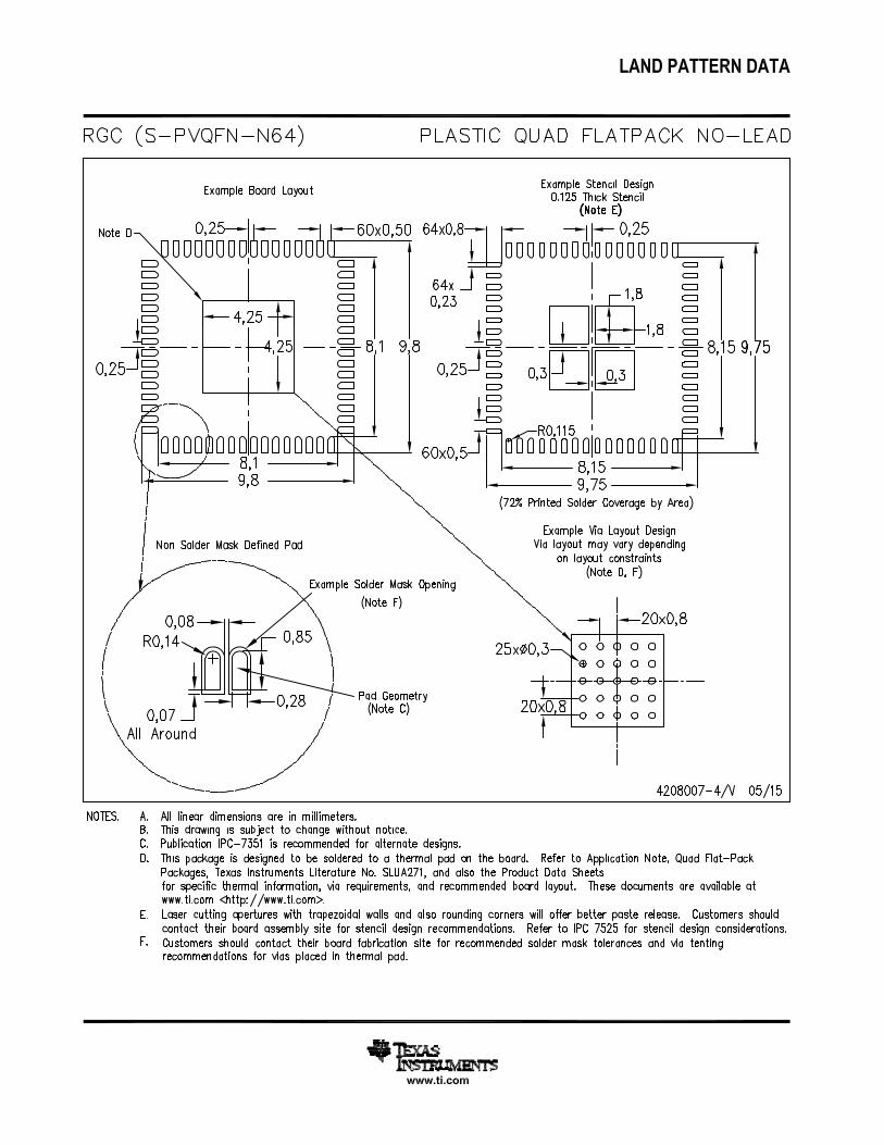

IMPORTANT NOTICE
Texas Instruments Incorporated (TI) reserves the right to make corrections, enhancements, improvements and other changes to itssemiconductor products and services per JESD46, latest issue, and to discontinue any product or service per JESD48, latest issue. Buyersshould obtain the latest relevant information before placing orders and should verify that such information is current and complete.TI’s published terms of sale for semiconductor products (http://www.ti.com/sc/docs/stdterms.htm) apply to the sale of packaged integratedcircuit products that TI has qualified and released to market. Additional terms may apply to the use or sale of other types of TI products andservices.Reproduction of significant portions of TI information in TI data sheets is permissible only if reproduction is without alteration and isaccompanied by all associated warranties, conditions, limitations, and notices. TI is not responsible or liable for such reproduceddocumentation. Information of third parties may be subject to additional restrictions. Resale of TI products or services with statementsdifferent from or beyond the parameters stated by TI for that product or service voids all express and any implied warranties for theassociated TI product or service and is an unfair and deceptive business practice. TI is not responsible or liable for any such statements.Buyers and others who are developing systems that incorporate TI products (collectively, “Designers”) understand and agree that Designersremain responsible for using their independent analysis, evaluation and judgment in designing their applications and that Designers havefull and exclusive responsibility to assure the safety of Designers' applications and compliance of their applications (and of all TI productsused in or for Designers’ applications) with all applicable regulations, laws and other applicable requirements. Designer represents that, withrespect to their applications, Designer has all the necessary expertise to create and implement safeguards that (1) anticipate dangerousconsequences of failures, (2) monitor failures and their consequences, and (3) lessen the likelihood of failures that might cause harm andtake appropriate actions. Designer agrees that prior to using or distributing any applications that include TI products, Designer willthoroughly test such applications and the functionality of such TI products as used in such applications.TI’s provision of technical, application or other design advice, quality characterization, reliability data or other services or information,including, but not limited to, reference designs and materials relating to evaluation modules, (collectively, “TI Resources”) are intended toassist designers who are developing applications that incorporate TI products; by downloading, accessing or using TI Resources in anyway, Designer (individually or, if Designer is acting on behalf of a company, Designer’s company) agrees to use any particular TI Resourcesolely for this purpose and subject to the terms of this Notice.TI’s provision of TI Resources does not expand or otherwise alter TI’s applicable published warranties or warranty disclaimers for TIproducts, and no additional obligations or liabilities arise from TI providing such TI Resources. TI reserves the right to make corrections,enhancements, improvements and other changes to its TI Resources. TI has not conducted any testing other than that specificallydescribed in the published documentation for a particular TI Resource.Designer is authorized to use, copy and modify any individual TI Resource only in connection with the development of applications thatinclude the TI product(s) identified in such TI Resource. NO OTHER LICENSE, EXPRESS OR IMPLIED, BY ESTOPPEL OR OTHERWISETO ANY OTHER TI INTELLECTUAL PROPERTY RIGHT, AND NO LICENSE TO ANY TECHNOLOGY OR INTELLECTUAL PROPERTYRIGHT OF TI OR ANY THIRD PARTY IS GRANTED HEREIN, including but not limited to any patent right, copyright, mask work right, orother intellectual property right relating to any combination, machine, or process in which TI products or services are used. Informationregarding or referencing third-party products or services does not constitute a license to use such products or services, or a warranty orendorsement thereof. Use of TI Resources may require a license from a third party under the patents or other intellectual property of thethird party, or a license from TI under the patents or other intellectual property of TI.TI RESOURCES ARE PROVIDED “AS IS” AND WITH ALL FAULTS. TI DISCLAIMS ALL OTHER WARRANTIES ORREPRESENTATIONS, EXPRESS OR IMPLIED, REGARDING RESOURCES OR USE THEREOF, INCLUDING BUT NOT LIMITED TOACCURACY OR COMPLETENESS, TITLE, ANY EPIDEMIC FAILURE WARRANTY AND ANY IMPLIED WARRANTIES OFMERCHANTABILITY, FITNESS FOR A PARTICULAR PURPOSE, AND NON-INFRINGEMENT OF ANY THIRD PARTY INTELLECTUALPROPERTY RIGHTS. TI SHALL NOT BE LIABLE FOR AND SHALL NOT DEFEND OR INDEMNIFY DESIGNER AGAINST ANY CLAIM,INCLUDING BUT NOT LIMITED TO ANY INFRINGEMENT CLAIM THAT RELATES TO OR IS BASED ON ANY COMBINATION OFPRODUCTS EVEN IF DESCRIBED IN TI RESOURCES OR OTHERWISE. IN NO EVENT SHALL TI BE LIABLE FOR ANY ACTUAL,DIRECT, SPECIAL, COLLATERAL, INDIRECT, PUNITIVE, INCIDENTAL, CONSEQUENTIAL OR EXEMPLARY DAMAGES INCONNECTION WITH OR ARISING OUT OF TI RESOURCES OR USE THEREOF, AND REGARDLESS OF WHETHER TI HAS BEENADVISED OF THE POSSIBILITY OF SUCH DAMAGES.Unless TI has explicitly designated an individual product as meeting the requirements of a particular industry standard (e.g., ISO/TS 16949and ISO 26262), TI is not responsible for any failure to meet such industry standard requirements.Where TI specifically promotes products as facilitating functional safety or as compliant with industry functional safety standards, suchproducts are intended to help enable customers to design and create their own applications that meet applicable functional safety standardsand requirements. Using products in an application does not by itself establish any safety features in the application. Designers mustensure compliance with safety-related requirements and standards applicable to their applications. Designer may not use any TI products inlife-critical medical equipment unless authorized officers of the parties have executed a special contract specifically governing such use.Life-critical medical equipment is medical equipment where failure of such equipment would cause serious bodily injury or death (e.g., lifesupport, pacemakers, defibrillators, heart pumps, neurostimulators, and implantables). Such equipment includes, without limitation, allmedical devices identified by the U.S. Food and Drug Administration as Class III devices and equivalent classifications outside the U.S.TI may expressly designate certain products as completing a particular qualification (e.g., Q100, Military Grade, or Enhanced Product).Designers agree that it has the necessary expertise to select the product with the appropriate qualification designation for their applicationsand that proper product selection is at Designers’ own risk. Designers are solely responsible for compliance with all legal and regulatoryrequirements in connection with such selection.Designer will fully indemnify TI and its representatives against any damages, costs, losses, and/or liabilities arising out of Designer’s non-compliance with the terms and provisions of this Notice.
Mailing Address: Texas Instruments, Post Office Box 655303, Dallas, Texas 75265Copyright © 2017, Texas Instruments Incorporated