mss 8051 subsystem - capital-micro.com · mss 8051 subsystem user guide 03/2013 capital...
TRANSCRIPT
MSS 8051 Subsystem
User Guide
03/2013
Capital microelectronics Co., Ltd

MSS 8051 System User Guide
http://www.capital-micro.com 1
Notes
Copyright © 2013 Capital Microelectronics, Inc. All
rights reserved.
No part of this document may be copied, transmitted,
transcribed, stored in a retrieval system, or translated
into any language or computer language, in any form or
by any means, electronic, mechanical, magnetic,
optical, chemical, manual or otherwise, without the
written permission of Capital Microelectronics, Inc. All
trademarks are the property of their respective
companies.
Version Number
CME8051UGE03
Contact Us
If you have any problems or requirements during using
our product, please contact
Capital Microelectronics, Inc. or your local
distributors, or send e-mail to
Warranty
The information in this document has been carefully
checked and is believed to be entirely reliable.
However, no responsibility is assumed for inaccuracies.
Furthermore, Capital Microelectronics, Inc. reserves the
right to discontinue or make changes, without prior
notice, to any products herein to improve reliability,
function, or design.
Capital Microelectronics, Inc. advises its customers to
obtain the latest version of the relevant information to
verify, before placing orders, that the information being
relied upon is current.
The product introduced in this book is not authorized
for use as critical components in life support devices
or systems without the express written approval of
Capital Microelectronics, Inc. As used herein: 1. Life
support devices or systems are devices or systems
that (a) are intended for surgical implant into the body
or (b) support or sustain life, and whose failure to
perform, when properly used in accordance with
instructions for use provided in the labeling, can be
reasonably expected to result in a significant injury to
the user. 2. A critical component is any component of
a life support device or system whose failure to
perform can be reasonably expected to cause the
failure of the life support device or system, or to affect
its safety or effectiveness.
Environmental Considerations
To avoid the harmful substances being
released into the environment or harming
human health, we encourage you to recycle
this product in an appropriate way to make
sure that most of the materials are reused or
recycled appropriately. Please contact your
local authorities for disposal or recycle
information.

MSS 8051 System User Guide
http://www.capital-micro.com 2
Contents
Notes .............................................................................................................................. 1
Version Number ............................................................................................................................. 1 Contact Us ...................................................................................................................................... 1 Warranty ......................................................................................................................................... 1 Environmental Considerations ....................................................................................................... 1
Contents ......................................................................................................................... 2
1 Features ................................................................................................................... 5
2 Overview .................................................................................................................. 6
2.1 Block Diagram ................................................................................................................. 7 2.2 Block Description ............................................................................................................. 7 2.3 Port Configuration ............................................................................................................ 8
2.3.1 Clocks ...................................................................................................................... 11 2.3.2 Reset ....................................................................................................................... 11
3 Memory .................................................................................................................. 13
3.1 Internal Memory and SFR ............................................................................................. 13 3.2 External Memory Interface (EMIF) ................................................................................ 14
3.2.1 Interface Description .............................................................................................. 14 3.2.2 Program Memory .................................................................................................... 14 3.2.3 External Data Memory............................................................................................ 15 3.2.4 EMIF Write and Read Cycle ................................................................................... 16
3.3 Memory Banking ............................................................................................................ 25
4 Special function registers (SFRs) ........................................................................ 26
4.1 Special Function Registers Locations ........................................................................... 26 4.2 SFR reset values ........................................................................................................... 27 4.3 SFR Description ............................................................................................................ 31
5 Instruction Set ....................................................................................................... 60
5.1 Instructions in Functional Order .................................................................................... 60 5.2 Instructions in hexadecimal order.................................................................................. 63 5.3 Read-Write-Modify instructions ..................................................................................... 64 5.4 Instruction duration calculation ...................................................................................... 65
6 Interrupt Controller ............................................................................................... 66
6.1 ISR ................................................................................................................................. 66 6.1.1 Block diagram ......................................................................................................... 66 6.1.2 Interrupt priority ...................................................................................................... 66
6.2 EXINT ............................................................................................................................ 68
7 Multiplication-Division Unit (MDU) ....................................................................... 71
7.1 MDU Operation Description .......................................................................................... 71
8 Timer0..................................................................................................................... 74
8.1 Block diagram ................................................................................................................ 74 8.1.1 Mode 0 and Mode 1 ............................................................................................... 74 8.1.2 Mode 2 .................................................................................................................... 74 8.1.3 Mode 3 .................................................................................................................... 75
8.2 Timer 0 Description ........................................................................................................ 75
MSS 8051 System User Guide
http://www.capital-micro.com 3
8.2.1 Timer/Counter 0 in Mode 0 .................................................................................... 75 8.2.2 Timer/Counter 0 in Mode 1 .................................................................................... 76 8.2.3 Timer/Counter 0 in Mode 2 .................................................................................... 76 8.2.4 Timer/Counter 0 in Mode 3 .................................................................................... 76
9 Timer1..................................................................................................................... 77
9.1 Block diagram ................................................................................................................ 77 9.1.1 Mode 0 and Mode 1 ............................................................................................... 77 9.1.2 Mode 2 .................................................................................................................... 77 9.1.3 Mode 3 .................................................................................................................... 77
9.2 Timer 1 Description ........................................................................................................ 78 9.2.1 Timer/Counter 1 in Mode 0 .................................................................................... 78 9.2.2 Timer/Counter 1 in Mode 1 .................................................................................... 78 9.2.3 Timer/Counter 1 in Mode 2 .................................................................................... 78 9.2.4 Timer/Counter 1 in Mode 3 .................................................................................... 79
10 Timer2 .............................................................................................................. 80
10.1 Block diagram ................................................................................................................ 80 10.2 Timer 2 Description ........................................................................................................ 80
10.2.1 Timer mode ............................................................................................................ 80 10.2.2 Event counter mode ............................................................................................... 80 10.2.3 Gated timer mode ................................................................................................... 81 10.2.4 Timer 2 reload ........................................................................................................ 81
10.3 Compare Description ..................................................................................................... 81 10.3.1 Compare Mode 0 .................................................................................................... 82 10.3.2 Compare Mode 1 .................................................................................................... 83
11 USART0(Serial0) ......................................................................................... 85
11.1 Block diagram ................................................................................................................ 85 11.2 Description ..................................................................................................................... 85
11.2.1 Baud Rate Generation ........................................................................................... 85 11.2.2 Operating Mode ...................................................................................................... 86 11.2.3 USART0 Multiprocessor Communication .............................................................. 88
12 USART1 ............................................................................................................ 89
12.1 Block diagram ................................................................................................................ 89 12.2 Description ..................................................................................................................... 89
12.2.1 Baud Rate Generation ........................................................................................... 89 12.2.2 USART1 operating modes ..................................................................................... 89 12.2.3 USART1 Multiprocessor Communication .............................................................. 91
13 Watchdog Timer .............................................................................................. 92
13.1 Block Diagram ............................................................................................................... 92 13.2 Description ..................................................................................................................... 92
14 Power Management and Reset Control Unit ................................................. 94
14.1 Power Managerment Description .................................................................................. 94 14.1.1 Idle mode ................................................................................................................ 94 14.1.2 Stop mode .............................................................................................................. 94
14.2 Reset control Description .............................................................................................. 94
15 Port ................................................................................................................... 95
16 I2C .................................................................................................................... 96
16.1 Block diagram ................................................................................................................ 96 16.2 Description ..................................................................................................................... 96
16.2.1 Operating Modes .................................................................................................... 97
MSS 8051 System User Guide
http://www.capital-micro.com 4
16.2.2 Arbitration ............................................................................................................... 97 16.2.3 Serial clock generator ............................................................................................ 97 16.2.4 Address comparator ............................................................................................... 98 16.2.5 Interrupt Generation ............................................................................................... 98 16.2.6 Special Function Registers..................................................................................... 98
16.3 System Management Bus Extension .......................................................................... 104
17 SPI .................................................................................................................. 106
17.1 Block diagram .............................................................................................................. 107 17.2 Description ................................................................................................................... 108
17.2.1 Special Function Registers................................................................................... 108 17.2.2 TR block ............................................................................................................... 109 17.2.3 Interrupt generation ...............................................................................................112
18 DMA ................................................................................................................ 114
18.1 Block diagram ...............................................................................................................114 18.2 Description ....................................................................................................................114
19 RTC ................................................................................................................. 117
19.1 Block diagram ...............................................................................................................117 19.2 Description ....................................................................................................................117
19.2.1 RTC Internal Special Function Registers ..............................................................117 19.2.2 Operating .............................................................................................................. 121
20 HOLD Interface .............................................................................................. 123
21 Revision History ............................................................................................ 125
MSS 8051 System User Guide
http://www.capital-micro.com 5
1 Features
MSS Subsystem is composed of 200MHz enhanced 8051 processor, embedded peripheral and SRAM. The features are as follow:
Enhanced 8051MCU - Reduced instruction cycle, 12 times in respect of standard 8051 MIPS, up to 200MHz - Compatible 8051 instruction system - Support up to 8Mbit data/code memory extension - Support hardware 32/16-bit MDU - On-chip debugger system (OCDS), online JTAG debugging - Up to 8M data/code memory
Peripheral - 3 16-bit Timers, Timer 2 can used as capture unit - 1 16-bit Watch Dog Timer - 1 I2C Interface - 1 SPI Interface - 2 USART - 4 input/output independend Port - RTC - 4 channels DMA - Hold interface
Stop, Idle Mode Power Management
MSS 8051 System User Guide
http://www.capital-micro.com 6
2 Overview
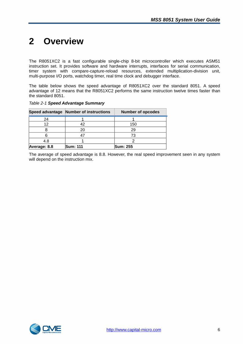
The R8051XC2 is a fast configurable single-chip 8-bit microcontroller which executes ASM51 instruction set. It provides software and hardware interrupts, interfaces for serial communication, timer system with compare-capture-reload resources, extended multiplication-division unit, multi-purpose I/O ports, watchdog timer, real time clock and debugger interface. The table below shows the speed advantage of R8051XC2 over the standard 8051. A speed advantage of 12 means that the R8051XC2 performs the same instruction twelve times faster than the standard 8051.
Table 2-1 Speed Advantage Summary
Speed advantage Number of instructions Number of opcodes
24 1 1 12 42 150 8 20 29 6 47 73
4.8 1 2
Average: 8.8 Sum: 111 Sum: 255
The average of speed advantage is 8.8. However, the real speed improvement seen in any system will depend on the instruction mix.
MSS 8051 System User Guide
http://www.capital-micro.com 7
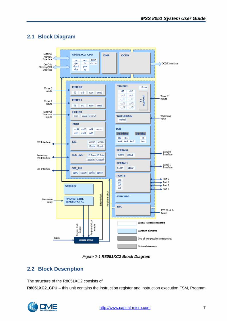
2.1 Block Diagram
Figure 2-1 R8051XC2 Block Diagram
2.2 Block Description
The structure of the R8051XC2 consists of:
R8051XC2_CPU – this unit contains the instruction register and instruction execution FSM, Program

MSS 8051 System User Guide
http://www.capital-micro.com 8
Counter and Data Pointer(s) registers, Stack Pointer register, the Arithmetic-Logic Unit with Accumulator, B and Program Status Word registers (ACC, B, PSW) (to provide all arithmetic - addition, subtraction, multiplication, division - and logic - bit- and byte-wise AND, OR, XOR – operations, the Program and External Data Memory interface, the On-Chip Data Memory and Special Function Registers interface, internally-generated wait-states, and interface to On-Chip Instrumentation
ISR – Interrupt Service Routine, provides interrupt enable and priority registers, priority decoder and interrupt vector generation - one of two options, or none
MDU – Multiplication-Division Unit, provides fast extended arithmetic operations like 16-bit multiplication, 32-bit division, shifting and normalizing
TIMER0 – provides a flexible 16-bit timer/counter with control and status register
TIMER1 – provides a flexible 16-bit timer/counter with control and status register
TIMER2 – contains the 16-bit Timer 2 with Capture-Compare Unit (4 compare/capture modules), with control and status register
SERIAL0 – contains Serial Port 0, a flexible synchronous/UART controller compatible to standard 80C51 serial port, with additional baud rate generator
SERIAL1 – provides the Serial Port 1, a simplified UART with its own baud rate generator
EXTINT – provides edge-detection hardware for all External Interrupts from 0 to 12
WATCHDOG – system supervisor, generating microcontroller reset when not refreshed in specified time
DMA – Direct Memory Access Controller, with 1 to 8 independent channels
PMURSTCTRL – Power Management Unit with Reset Control Unit, generates clock gates for the main CPU and for peripherals, serves the Power Down Modes: IDLE and STOP; generates internal synchronous reset signal (upon external reset or watchdog timer overflow)
WAKEUPCTRL – Wake-Up From Power-Down Mode Control Unit, provides external interrupts ―int0‖ and ―int1‖ service during power-down modes, to be used by the PMURSTCTRL module
PORTS – parallel I/O port controller, serves up to 4 parallel 8-bit I/O ports to be used in combination with off-core buffers, compatible to classic 80C51, but without multiplexed memory feature and without alternate functions (if needed, to be combined off-core)
SYNCNEG – contains flip-flops to synchronize all asynchronous inputs such as hardware reset or external interrupts
SFRMUX – provides a common bus multiplexer for all the internal and external Special Function Registers
I2C – provides a flexible master – slave I2C interface
SPI – provides a flexible master – slave SPI interface
OCDS – provides development functions such as run/stop/step control and software/hardware breakpoints of program execution
RTC – provides Real Time Clock function
2.3 Port Configuration
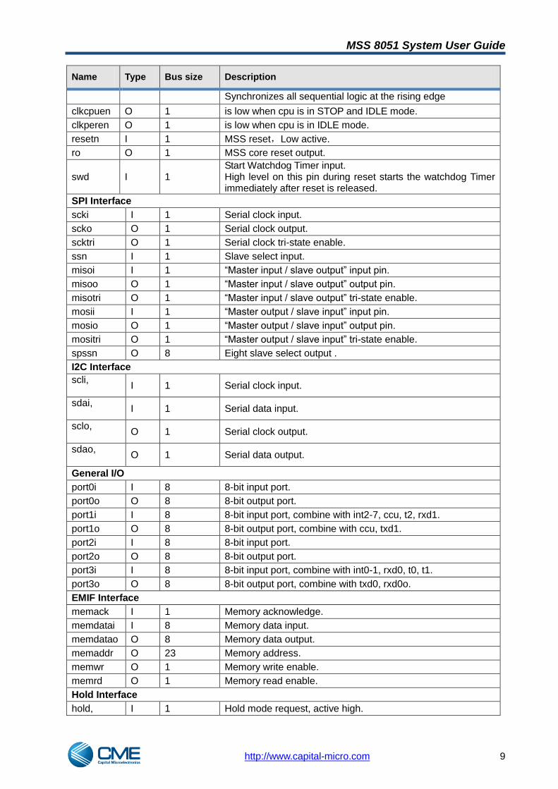
Table 2-2 8051 Port Definition
Name Type Bus size Description
Global Interface
clkcpu I 1 Engine clock
MSS 8051 System User Guide
http://www.capital-micro.com 9
Name Type Bus size Description
Synchronizes all sequential logic at the rising edge
clkcpuen O 1 is low when cpu is in STOP and IDLE mode.
clkperen O 1 is low when cpu is in IDLE mode.
resetn I 1 MSS reset,Low active.
ro O 1 MSS core reset output.
swd I 1 Start Watchdog Timer input. High level on this pin during reset starts the watchdog Timer immediately after reset is released.
SPI Interface
scki I 1 Serial clock input.
scko O 1 Serial clock output.
scktri O 1 Serial clock tri-state enable.
ssn I 1 Slave select input.
misoi I 1 ―Master input / slave output‖ input pin.
misoo O 1 ―Master input / slave output‖ output pin.
misotri O 1 ―Master input / slave output‖ tri-state enable.
mosii I 1 ―Master output / slave input‖ input pin.
mosio O 1 ―Master output / slave input‖ output pin.
mositri O 1 ―Master output / slave input‖ tri-state enable.
spssn O 8 Eight slave select output .
I2C Interface
scli,
I 1 Serial clock input.
sdai,
I 1 Serial data input.
sclo,
O 1 Serial clock output.
sdao,
O 1 Serial data output.
General I/O
port0i I 8 8-bit input port.
port0o O 8 8-bit output port.
port1i I 8 8-bit input port, combine with int2-7, ccu, t2, rxd1.
port1o O 8 8-bit output port, combine with ccu, txd1.
port2i I 8 8-bit input port.
port2o O 8 8-bit output port.
port3i I 8 8-bit input port, combine with int0-1, rxd0, t0, t1.
port3o O 8 8-bit output port, combine with txd0, rxd0o.
EMIF Interface
memack I 1 Memory acknowledge.
memdatai I 8 Memory data input.
memdatao O 8 Memory data output.
memaddr O 23 Memory address.
memwr O 1 Memory write enable.
memrd O 1 Memory read enable.
Hold Interface
hold, I 1 Hold mode request, active high.

MSS 8051 System User Guide
http://www.capital-micro.com 10
Name Type Bus size Description
holda O 1 Hold mode acknowledge signal.
intoccur O 1 Interrupt occure in hold mode signal.
waitstaten O 1 Waitstate indicator, active low when 8051 performs a wait cycle.
All the ports are connected to SoC fabric. The EMIF unites the program and external data memory interfaces of the R8051XC2 to one memory interface. Some function pins, such as: external interrupt1, USART0, USART1, Timer 0~2, and Compare – Capture Unit, share pins with port1 and port3. The following shows the details. Table 2-3 Port Pin Multiplex
Name Type Polarity Bus size
Alternate Port
Description
External Interrupts Inputs
int0 I Low/Fall port3i[2] External interrupt 0
int1 I Low/Fall port3i[3] External interrupt 1
int2 I Fall/Rise port1i[4] External interrupt 2
int3 I Fall/Rise port1i[0] External interrupt 3
int4 I Rise port1i[1] External interrupt 4
int5 I Rise port1i[2] External interrupt 5
int6 I Rise port1i[3] External interrupt 6
int7 I Rise port1i[6] External interrupt 7
Serial 0 Interface
rxd0i I 1 port3i[0] Serial 0 receive data
rxd0o O 1 port3o[0] Serial 0 transmit data
txd0 O 1
port3o[1] Serial 0 transmit data or receive clock in mode 0
Serial 1 Interface
rxd1 I 1 port1i[0] Serial 1 receive data
txd1 O 1 port1o[1] Serial 1 transmit data
Timers Inputs
t0 I Fall port3i[4] Timer 0 external input
t1 I Fall port3i[5] Timer 1 external input
t2 I Fall port1i[7] Timer 2 external input
t2ex I Fall port1i[5] Timer 2 capture trigger
Compare – Capture Unit
cc(0) I Rise/Fall port1i[0] Compare/Capture 0 input
cc(1) I Rise port1i[1] Compare/Capture 1 input
cc(2) I Rise port1i[2] Compare/Capture 2 input
cc(3) I Rise port1i[3] Compare/Capture 3 input
Ccubus[0] O 1 port1o[0] Compare/Capture 0 Output
Ccubus[1] O 1 port1o[1] Compare/Capture 1 Output
Ccubus[2] O 1 port1o[2] Compare/Capture 2 Output
Ccubus[3] O 1 port1o[3] Compare/Capture 3 Output

MSS 8051 System User Guide
http://www.capital-micro.com 11
2.3.1 Clocks
Table 2-4 R8051XC2 Clock Inputs
Clock Type Polarity Description
clkcpu I Rise
Engine clock Pulse for internal circuits, which are stopped
when R8051XC2 is in IDLE or STOP mode
clkper I Rise
Peripheral clock Pulse for internal circuits, which are stopped
when R8051XC2 is in STOP mode
tck I Rise/Fall Test (Debug) Clock IEEE1149.1 port clock input.
rtcx I Rise/Fall RTC Clock Pulse for the Real Time Clock (should be 32,768kHz).
The ‖clkcpu‖ is a clock signal dedicated to main R8051XC2 modules like CPU, DMA, OCDS (On Chip Debug System) and SOFTRSTCTRL (Software Reset), which are stopped in both IDLE and STOP power-down modes. It should be generated outside the core the way that it runs when the ―clkcpuen‖ output is active and stopped otherwise. The‖clkper‖ is a clock signal dedicated to R8051XC2 peripheral modules like Interrupt Service Routine, Serial Ports, Timers, Watchdog Timer, Multiplication/Division Unit, Parallel I/O Ports, External Interrupts, I2C and SPI, which are stopped in the STOP mode. It should be generated outside the core the way that it runs when the ―clkperen‖ output is active and stopped otherwise. Both ―clkcpu‖ and ―clkper‖ have to be balanced since there is no synchronization logic between their domains. The‖tck‖ is a clock signal dedicated to R8051XC2 OCDS module. It is used to synchronize the transmission through OCDS port (IEEE1149.1 compliant). Both edges of this clock are used inside the OCDS module. The‖rtcx‖ is a clock signal dedicated to R8051XC2 Real Time Clock module. It should be connected to a 32,768 kHz oscillator to provide valid time count. The ―rtcx‖ triggers the RTC time registers at the rising edge.
2.3.2 Reset
(1) Reset Description
Upon reset, all the registers and flip-flops of the R8051XC2 are put into known state. The Program Memory, External Data Memory, On-Chip Data Memory (Internal Data Memory) and Special Function Register interface control outputs are set inactive. The Program Counter is loaded with zero. During reset, the ―swd‖ input is sampled to enable or disable the ―automatic start‖ of the Watchdog Timer, when selected during core configuration. Only the synchronization flip-flops gathered in the SYNCNEG module have no reset.
(2) Hardware Reset

MSS 8051 System User Guide
http://www.capital-micro.com 12
The R8051XC2 core contains a single ―reset‖ input. It should be active (high) for at least two periods of ―clkper‖ clock to ensure that it will be sampled active at least once. The ―reset‖ input is routed to the SYNCNEG subcomponent and sampled there at every peripheral clock (―clkper‖) rising edge. The main internal synchronous ―rst‖ signal is generated from the input samples of ―reset‖, software reset, watchdog overflow and OCDS. The ―rst‖ signal is routed to all clock domains in the core and it forces all synchronous logic to a known state. Additionally the R8051XC2 can be reset using the ―trst‖ input to the OCDS module, if implemented. It is used asynchronously to reset the TAP machine of the OCDS, and also generates an internal reset to be OR-ed with the ―rst‖ signal mentioned above. If the Real Time Clock is implemented, there is the ―rtcreset‖ input implemented to provide asynchronous reset to the flip-flops and registers which are triggered by the ―rtcx‖ clock. Those registers / flip-flops should not be affected by the main hardware reset in order to maintain valid clock count despite of the system activity.
(3) Software Reset
For more details on Software Reset feature see section 15.

MSS 8051 System User Guide
http://www.capital-micro.com 13
3 Memory
The R8051XC2 microcontroller core incorporates the Harvard architecture, with separate code and data spaces. Memory organization is similar to that of the industry standard 8051. There are three memory areas: Program Memory, External Data Memory (External RAM) and Internal Data Memory (Internal RAM). In addition, MSS integrates 256 bytes Internal Data Memory. The R8051XC2 microcontroller core can be configured to extend both Program Memory and External Data Memory total up to 8MB by means of dedicated page address register.
Internal RAM SFR
Only indirect
addressing
Only direct
addressing
Bit-addressable space (bits 00h-7Fh)Registers bank
4x8 bytes000000h00001Fh00002Fh
00007Fh
0000FFh
common
bank1
bank2
bank255
007FFFh008000h
00FFFFh010000h
010FFFh
7FFFFFh
7F8000h
Figure 3-1 R8051XC2 Memory Map
3.1 Internal Memory and SFR
Depending on configuration the R8051XC2 internal data memory interface services up to 256 bytes of off-core data memory. The memory space accommodates also 128 bytes of Special Function Registers (see figure below). Addresses lower than 80h access lower 128 bytes of internal data memory. Both direct or indirect addressing can be used in this case. Indirect addressing of locations higher than 7Fh accesses upper 128 bytes of internal data memory, while direct addressing of locations higher than 7Fh accesses SFR space.

MSS 8051 System User Guide
http://www.capital-micro.com 14
The lower 128 bytes contain work registers (00h … 1Fh) and bit-addressable memory (20h … 2Fh). The lowest 32 bytes form four banks, each consisting of eight registers (R0-R7). Two bits of the program memory status word (PSW) select which bank is in use. The next 16 bytes of memory form a block of bit-addressable memory, accessible via 00h-7Fh addresses (Table 4-2 ). The figure below shows the internal 256-byte memory map. The memory space accommodates 128 bytes of Special Function Registers. Addresses lower than 80h access lower 128 bytes of internal data memory. Both direct and indirect addressing can be used in this case. Indirect addressing of locations higher than 7Fh accesses upper 128 bytes of internal data memory, while direct addressing of locations higher than 7Fh accesses SFR space. The lower 128 bytes contain work registers (00h … 1Fh) and bit-addressable memory (20h …2Fh). The lowest 32 bytes form four banks, each consisting of eight registers (R0-R7). Two bits of the program memory status word (PSW) select which bank is in use. The next 16 bytes of memory form a block of bit-addressable memory, accessible via 00h-7Fh addresses (see 1HTable 4-2 Bit-addressable space).
Internal RAM SFR
Only indirect
addressing
Only direct
addressing
Bit-addressable space
(bits 00h-7Fh)
Registers bank
4x8 bytes00h1Fh
2Fh
7Fh
FFh
Figure 3-2 Internal memory mapping
3.2 External Memory Interface (EMIF)
3.2.1 Interface Description
The R8051XC2 contains interface to External Memory which is used to access external data memory and program memory. The interface consists of the 23-bit wide address bus ―memaddr‖, the 8-bit input data bus ―memdatai‖, the 8-bit output data bus ―memdatao‖, and control signals ―memrd‖, ―memwr‖, ―mempsrd‖, ―mempswr‖, ―memack‖, ―mempsack‖. It spreads program memory and external data memory total up to 8MB. The External Bus Interface shares both Program Memory and External Data Memory and services Program Memory when ―mempsrd‖ or ―mempswr‖ signals are active. The Program Memory and External Data Memory share the External Bus Interface, which services data memory when ―memrd‖ or ―memwr‖ signals are active.
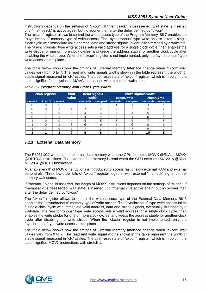
3.2.2 Program Memory
Program memory is read when the CPU performs instruction fetch or constant read via MOVC instruction, and is written when R8051XC2 is in Program Memory Write Mode using MOVX instruction. Three bits of high-order half of ―ckcon‖ register together with external ―mempsack‖ signal control memory wait states. If ―mempsack‖ signal is asserted, the length of fetch cycle and MOVC
MSS 8051 System User Guide
http://www.capital-micro.com 15
instructions depends on the settings of ―ckcon‖. If ―mempsack‖ is deasserted, wait state is inserted until ―mempsack‖ is active again, but no sooner than after the delay defined by ―ckcon‖. The ―ckcon‖ register allows to control the write access type of the Program Memory. Bit 7 enables the ―asynchronous‖ memory-type of write access. The ―synchronous‖ type write access takes a single clock cycle with immediate valid address, data and strobe signals, eventually stretched by a waitstate. The ―asynchronous‖ type write access sets a valid address for a single clock cycle, then enables the write strobe for one or more clock cycles, and keeps the address stable for another clock cycle after disabling the write strobe. When the ―ckcon‖ register is not implemented, only the ―synchronous‖ type write access takes place. The table below shows how the timings of External Memory Interface change when ―ckcon‖ wait values vary from 0 to 7. The read and write signals widths shown in the table represent the width of stable signal measured in ―clk‖ cycles. The post-reset state of ―ckcon‖ register, which is in bold in the table, signifies fetch cycles or MOVC instructions with maximum waitstates.
Table 3-1 Program Memory Wait State Cycle Width
3.2.3 External Data Memory
The R8051XC2 writes to the external data memory when the CPU executes MOVX @Ri,A or MOVX @DPTR,A instructions. The external data memory is read when the CPU executes MOVX A,@Ri or MOVX A,@DPTR instructions.
A variable length of MOVX instructions is introduced to access fast or slow external RAM and external peripherals. Three low-order bits of ―ckcon‖ register together with external ―mamack‖ signal control memory wait states.
If ―memack‖ signal is asserted, the length of MOVX instructions depends on the settings of ―ckcon‖. If ―mempsack‖ is deasserted, wait state is inserted until ―memack‖ is active again, but no sooner than after the delay defined by ―ckcon‖.
The ―ckcon‖ register allows to control the write access type of the External Data Memory. Bit 3 enables the ―asynchronous‖ memory-type of write access. The ―synchronous‖ type write access takes a single clock cycle with immediate valid address, data and strobe signals, eventually stretched by a waitstate. The ―asynchronous‖ type write access sets a valid address for a single clock cycle, then enables the write strobe for one or more clock cycles, and keeps the address stable for another clock cycle after disabling the write strobe. When the ―ckcon‖ register is not implemented, only the ―synchronous‖ type write access takes place.
The table below shows how the timings of External Memory Interface change when ―ckcon‖ wait values vary from 0 to 7. The read and write signal widths shown in the table represent the width of stable signal measured in ―clk‖ cycles. The post-reset state of ―ckcon‖ register, which is in bold in the table, signifies MOVX instructions with stretch 1.

MSS 8051 System User Guide
http://www.capital-micro.com 16
Table 3-2 External Data Memory Wait State Cycle Width
3.2.4 EMIF Write and Read Cycle
The R8051XC2 core contains interface to External Memory consisting of the 23-bit wide address bus ―memaddr‖, the 8-bit input data bus ―memdatai‖, the 8-bit output data bus ―memdatao‖, and control signals ―memrd‖, ―memwr‖, ―mempsrd‖, ―mempswr‖, ―memack‖, ―mempsack‖. The control signals ―memrd‖, ―memwr‖, ―memack‖ and ―mempsrd‖, ―mempswr‖, ―mempsack‖ are used to access external data memory and program memory. But the control signals ―memrd‖, ―memwr‖, ―memack‖ and ―mempsrd‖, ―mempswr‖, ―mempsack‖ are oried in the MSS system to ―memrd‖, ―memwr‖, ―memack‖ for user to use. So the external data memory and program memory have the united memory space and one memory bus for user but the core has independend external data memory and program memory space. Note:
User must not overlap the external data memory and program memory space. The xdata operation will modify the code and cause the 8051 running fault if the external data memory and program memory have overlap.
(1) Program Memory Read Cycle
The execution of instruction N is performed during the fetch of instruction N+1.
Figure 3-3 Memory Read Cycle without Wait States
Note: N - address of actually executed instruction (N) - Instruction fetched from address N N+1 - address of next instruction read sample - point of capturing data into internal register

MSS 8051 System User Guide
http://www.capital-micro.com 17
Figure 3-4 Memory Read Cycle with 5 Wait States Note: N - address of actually executed instruction
(N) - instruction fetched from address N read sample - point of capturing data into internal register
Figure 3-5 Memory Read Cycle with 5 Wait States, Delayed by Mempsack Note: N - address of actually executed instruction (N) - instruction fetched from address N read sample - point of capturing data into internal register
(2) Program Memory write cycle
(N) is the instruction that performs program memory write.
MSS 8051 System User Guide
http://www.capital-micro.com 18
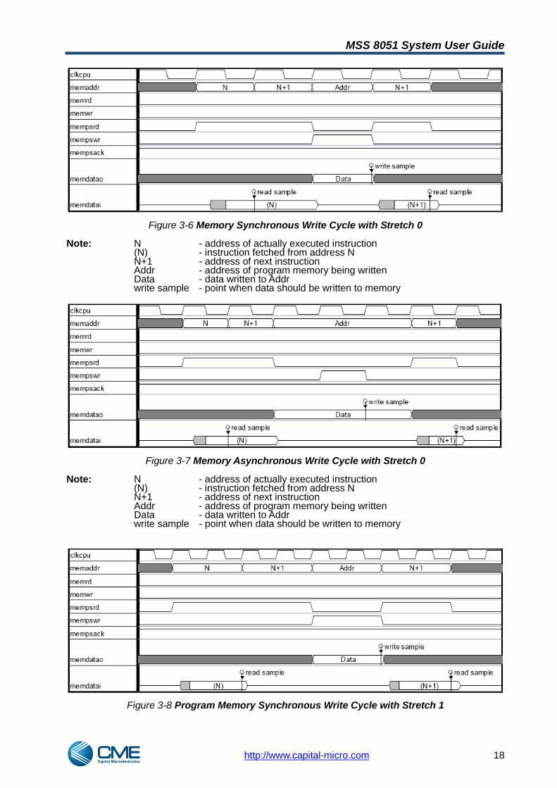
Figure 3-6 Memory Synchronous Write Cycle with Stretch 0 Note: N - address of actually executed instruction (N) - instruction fetched from address N N+1 - address of next instruction Addr - address of program memory being written Data - data written to Addr write sample - point when data should be written to memory
Figure 3-7 Memory Asynchronous Write Cycle with Stretch 0 Note: N - address of actually executed instruction (N) - instruction fetched from address N N+1 - address of next instruction Addr - address of program memory being written Data - data written to Addr write sample - point when data should be written to memory
Figure 3-8 Program Memory Synchronous Write Cycle with Stretch 1
MSS 8051 System User Guide
http://www.capital-micro.com 19
Note: N - address of actually executed instruction (N) - instruction fetched from address N N+1 - address of next instruction
Addr - address of program memory being written Data - data written to Addr write sample - point when data should be written to memory
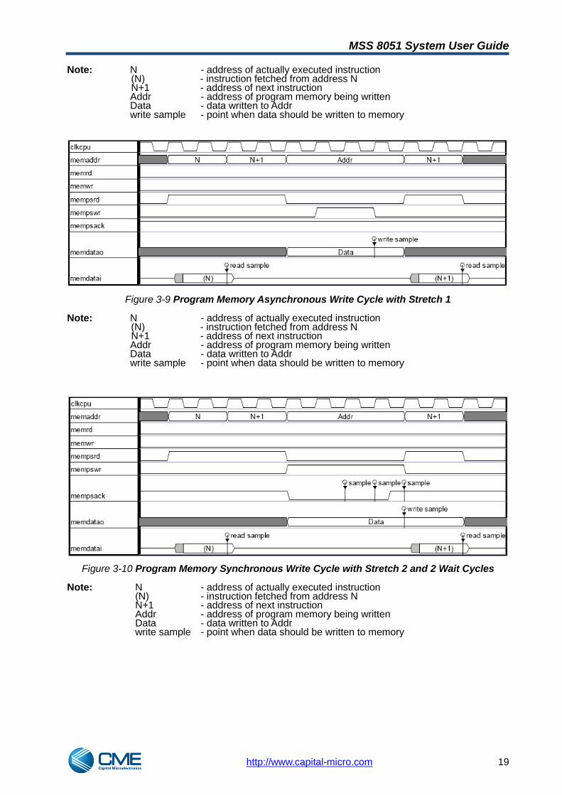
Figure 3-9 Program Memory Asynchronous Write Cycle with Stretch 1 Note: N - address of actually executed instruction
(N) - instruction fetched from address N N+1 - address of next instruction
Addr - address of program memory being written Data - data written to Addr write sample - point when data should be written to memory
Figure 3-10 Program Memory Synchronous Write Cycle with Stretch 2 and 2 Wait Cycles Note: N - address of actually executed instruction (N) - instruction fetched from address N N+1 - address of next instruction Addr - address of program memory being written Data - data written to Addr write sample - point when data should be written to memory
MSS 8051 System User Guide
http://www.capital-micro.com 20
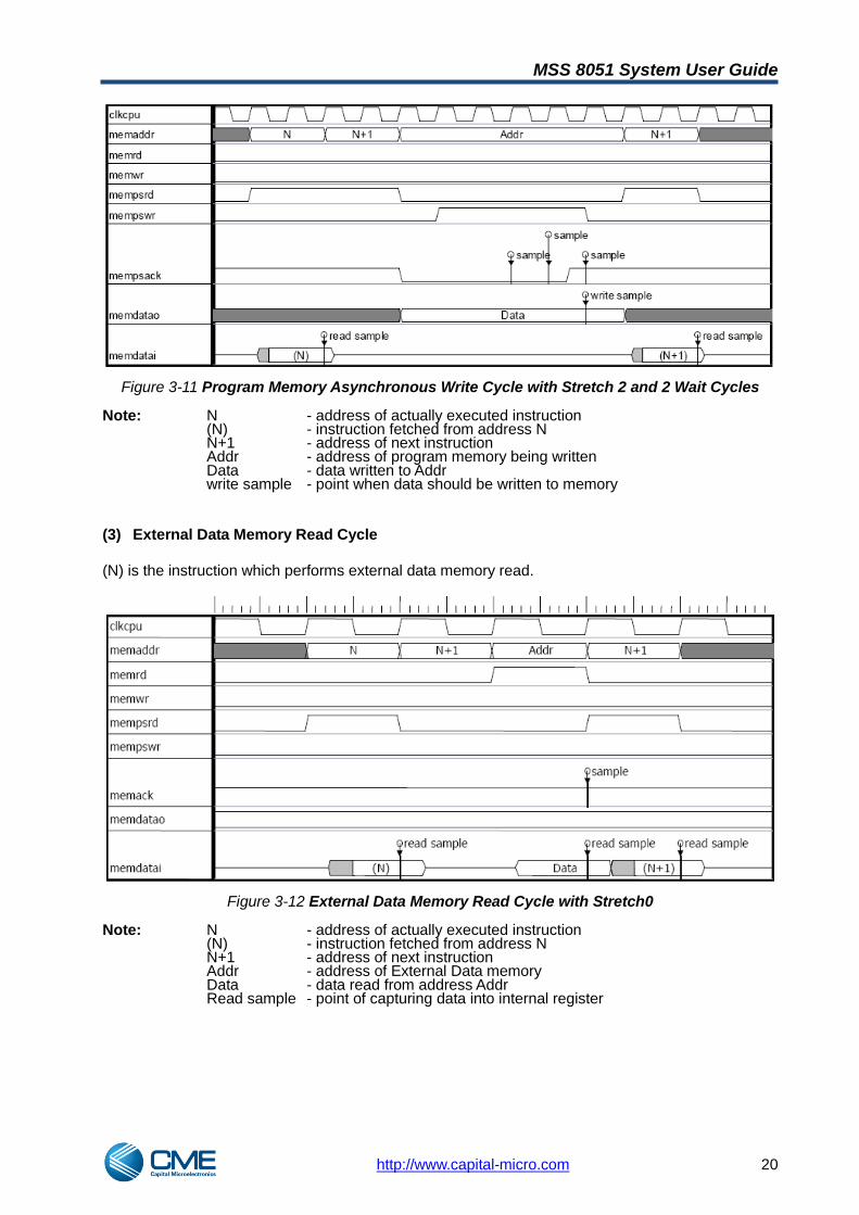
Figure 3-11 Program Memory Asynchronous Write Cycle with Stretch 2 and 2 Wait Cycles Note: N - address of actually executed instruction (N) - instruction fetched from address N N+1 - address of next instruction Addr - address of program memory being written Data - data written to Addr write sample - point when data should be written to memory
(3) External Data Memory Read Cycle
(N) is the instruction which performs external data memory read.
Figure 3-12 External Data Memory Read Cycle with Stretch0 Note: N - address of actually executed instruction (N) - instruction fetched from address N N+1 - address of next instruction Addr - address of External Data memory Data - data read from address Addr Read sample - point of capturing data into internal register
MSS 8051 System User Guide
http://www.capital-micro.com 21
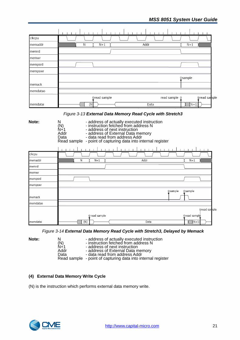
Figure 3-13 External Data Memory Read Cycle with Stretch3 Note: N - address of actually executed instruction (N) - instruction fetched from address N N+1 - address of next instruction Addr - address of External Data memory Data - data read from address Addr Read sample - point of capturing data into internal register
Figure 3-14 External Data Memory Read Cycle with Stretch3, Delayed by Memack Note: N - address of actually executed instruction (N) - instruction fetched from address N N+1 - address of next instruction Addr - address of External Data memory Data - data read from address Addr Read sample - point of capturing data into internal register
(4) External Data Memory Write Cycle
(N) is the instruction which performs external data memory write.
MSS 8051 System User Guide
http://www.capital-micro.com 22
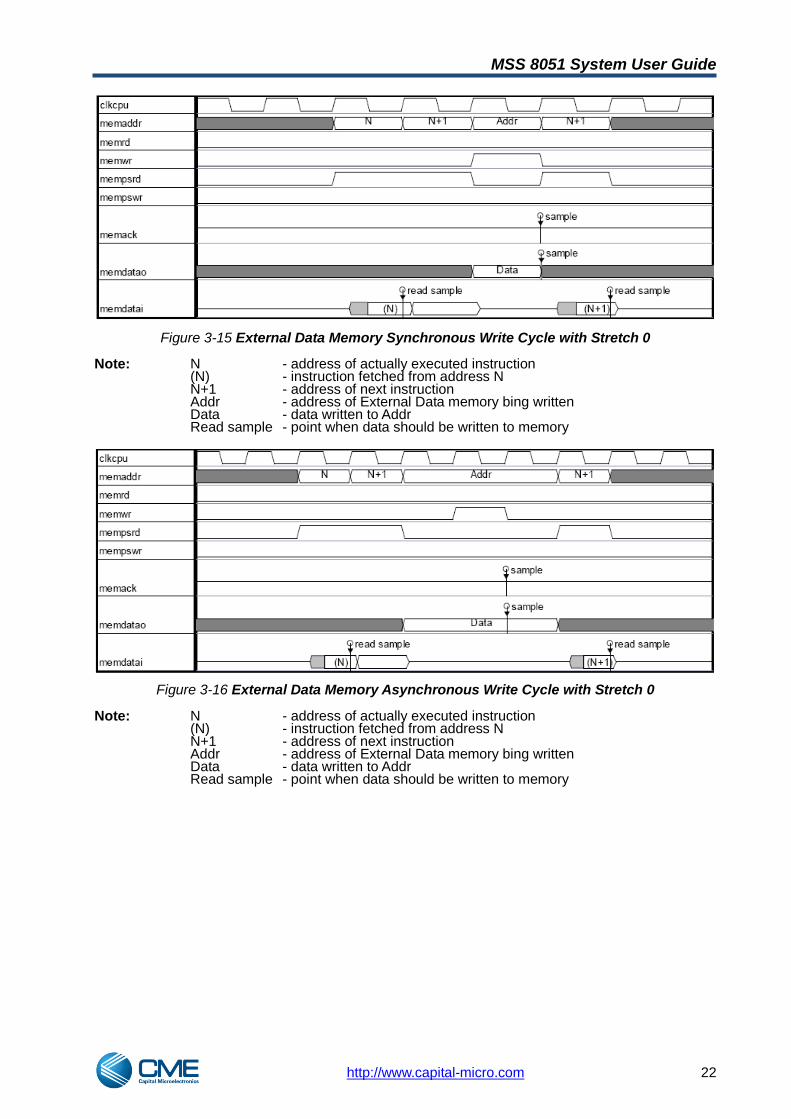
Figure 3-15 External Data Memory Synchronous Write Cycle with Stretch 0 Note: N - address of actually executed instruction (N) - instruction fetched from address N N+1 - address of next instruction Addr - address of External Data memory bing written Data - data written to Addr Read sample - point when data should be written to memory
Figure 3-16 External Data Memory Asynchronous Write Cycle with Stretch 0 Note: N - address of actually executed instruction (N) - instruction fetched from address N N+1 - address of next instruction Addr - address of External Data memory bing written Data - data written to Addr Read sample - point when data should be written to memory

MSS 8051 System User Guide
http://www.capital-micro.com 23
Figure 3-17 External Data Memory Synchronous Write Cycle with Stretch 1 Note: N - address of actually executed instruction (N) - instruction fetched from address N N+1 - address of next instruction Addr - address of External Data memory bing written Data - data written to Addr Read sample - point when data should be written to memory
Figure 3-18 External Data Memory Asynchronous Write Cycle with Stretch 1 Note: N - address of actually executed instruction (N) - instruction fetched from address N N+1 - address of next instruction Addr - address of External Data memory bing written Data - data written to Addr Read sample - point when data should be written to memory
MSS 8051 System User Guide
http://www.capital-micro.com 24
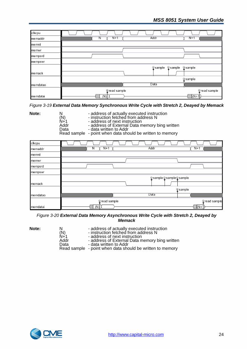
Figure 3-19 External Data Memory Synchronous Write Cycle with Stretch 2, Deayed by Memack Note: N - address of actually executed instruction (N) - instruction fetched from address N N+1 - address of next instruction Addr - address of External Data memory bing written Data - data written to Addr Read sample - point when data should be written to memory
Figure 3-20 External Data Memory Asynchronous Write Cycle with Stretch 2, Deayed by Memack
Note: N - address of actually executed instruction (N) - instruction fetched from address N N+1 - address of next instruction Addr - address of External Data memory bing written Data - data written to Addr Read sample - point when data should be written to memory

MSS 8051 System User Guide
http://www.capital-micro.com 25
3.3 Memory Banking
When 8051 does not work as banking, memory can reach to 64KB (0000h~FFFFh). When works as banking using the PAGESEL and D_PAGESEL to select the program and data memory bank, memory mapping shows below. For detail settings, please refer to Section 4 SFR description 2H(10) and 3H(11).
common
000000h
bank1
bank2
bank255
007FFFh008000h
00FFFFh010000h
010FFFh
7FFFFFh
7F8000h
Memory banking
Figure 3-21 code/external data memory banking
The table below lists the bank logic address, physical address and Keil expression relation.
Table 3-3 Logic and Physical Memory Relation
Program/Xdata
Bank
Physical Address
(memaddr[22:0])
Logic
Address
(Keil Memory Windows)
Keil Code
0 x:0x00000 x:0x07FFF
x:0x00000 x:0x07FFF
D_PAGESEL= 0 / PAGESEL= 0 x:0x00000 x:0x07FFF
1 x:0x08000 x:0x0FFFF
x:0x18000 x:0x1FFFF
D_PAGESEL= 1 / PAGESEL= 1 x:0x08000 x:0x0FFFF
2 x:0x10000 x:0x17FFF
x:0x28000 x:0x2FFFF
D_PAGESEL= 2 / PAGESEL= 2 x:0x08000 x:0x0FFFF
3 x:0x18000 x:0x1FFFF
x:0x38000 x:0x3FFFF
D_PAGESEL= 3 / PAGESEL= 3 x:0x08000 x:0x0FFFF
4 x:0x20000 x:0x27FFF
x:0x48000 x:0x4FFFF
D_PAGESEL= 4 / PAGESEL= 4 x:0x08000 x:0x0FFFF
..

MSS 8051 System User Guide
http://www.capital-micro.com 26
4 Special function registers (SFRs)
4.1 Special Function Registers Locations
The table below shows the map of SFR.
Table 4-1 SFR locations
Hex/ Bin
X000 X001 X010 X011 X100 X101 X110 X111 Bin/ Hex
F8 FF
F0 b srst F7
E8 Umd0 Umd1 Umd2 Umd3 Umd4 Umd5 Uarcon EF
E0 Uacc Uspsta Uspcon Uspdat Uspssn Urtccmd Urtcsel Urtcdata E7
D8 adcon i2cdat i2cadr i2ccon i2csta smb_sel smb_dst DF
D0 Upsw ien4 D7
C8 Ut2con Ucrcl Ucrch Utl2 Uth2 CF
C0 ircon ccen ccl1 cch1 ccl2 cch2 ccl3 cch3 C7
B8 Uien1 Uip1 Us0relh Us1relh BF
B0 Up3 dmac0 dmac1 dmac2 dmasel dmam0 dmam1 B7
A8 ien0 ip0 s0rell AF
A0 Up2 dmas0 dmas1 dmas2 dmat0 dmat1 dmat2 A7
98 Us0con Us0buf Uien2 Us1con Us1buf Us1rell 9F
90 p1 dps pagesel d_pagesel 97
88 Utcon Utmod Utl0 Utl1 Uth0 Uth1 Uckcon 8F
80 p0 sp dpl dph dpl1 dph1 wdtrel pcon 87
The 16 addresses from SFR space are both byte- and bit-addressable. The bit-addressable SFRs are registers which addresses end with 000‘b (80‘h, 88‘h, 90‘h … F8‘h). Those 16 registers (128 bits) together with 128 bits from internal data memory (locations 20‘h … 2F‘h) form the bit-addressable space (refer to the table below). Table 4-2 Bit-addressable space
Hex/ Bin
X000 X001 X010 X011 X100 X101 X110 X111 Bin/ Hex
SFR
F8 FF
F0 b.0 b.1 b.2 b.3 b.4 b.5 b.6 b.7 F7
E8 EF
E0 acc.0 acc.1 acc.2 acc.3 acc.4 acc.5 acc.6 acc.7 E7
D8 adcon.0 adcon.1 adcon.2 adcon.3 adcon.4 adcon.5 adcon.6 adcon.7 DF
D0 psw.0 psw.1 psw.2 psw.3 psw.4 psw.5 psw.6 psw.7 D7
C8 t2con.0 t2con.1 t2con.2 t2con.3 t2con.4 t2con.5 t2con.6 t2con.7 CF
C0 ircon.0 ircon.1 ircon.2 ircon.3 ircon.4 ircon.5 ircon.6 ircon.7 C7

MSS 8051 System User Guide
http://www.capital-micro.com 27
Hex/ Bin
X000 X001 X010 X011 X100 X101 X110 X111 Bin/ Hex
B8 ip.0 /ien1.0
ip.1 /ien1.1
ip.2 /ien1.2
ip.3 /ien1.3
ip.4 /ien1.4
ip.5 /ien1.5
ip.6 /ien1.6
ip.7 /ien1.7
BF
B0 p3.0 p3.1 p3.2 p3.3 p3.4 p3.5 p3.6 p3.7 B7
A8 ien0.0 ien0.1 ien0.2 ien0.3 ien0.4 ien0.5 ien0.6 ien0.7 AF
A0 p2.0 p2.1 p2.2 p2.3 p2.4 p2.5 p2.6 p2.7 A7
98 s0con.0 s0con.1 s0con.2 s0con.3 s0con.4 s0con.5 s0con.6 s0con.7 9F
90 p1.0 p1.1 p1.2 p1.3 p1.4 p1.5 p1.6 p1.7 97
88 tcon.0 tcon.1 tcon.2 tcon.3 tcon.4 tcon.5 tcon.6 tcon.7 8F
80 p0.0 p0.1 p0.2 p0.3 p0.4 p0.5 p0.6 p0.7 87
Internal RAM
78 2Fh.0 2Fh.1 2Fh.2 2Fh.3 2Fh.4 2Fh.5 2Fh.6 2Fh.7 7F
70 2Eh 77
68 2Dh 6F
60 2Ch 67
58 2Bh 5F
50 2Ah 57
48 29h 4F
40 28h 47
38 27h 3F
30 26h 37
28 25h 2F
20 24h 27
18 23h 1F
10 22h 17
08 21h.0 21h.1 21h.2 21h.3 21h.4 21h.5 21h.6 21h.7 0F
00 20h.0 20h.1 20h.2 20h.3 20h.4 20h.5 20h.6 20h.7 07
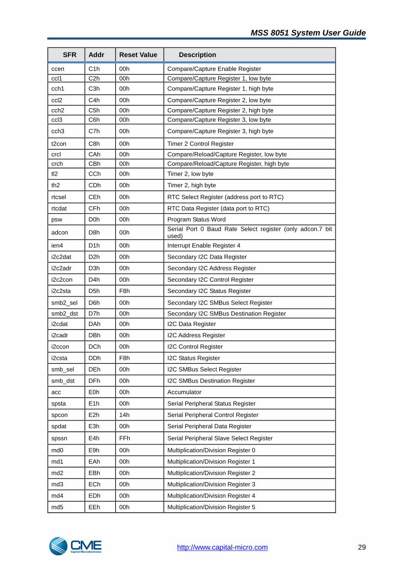
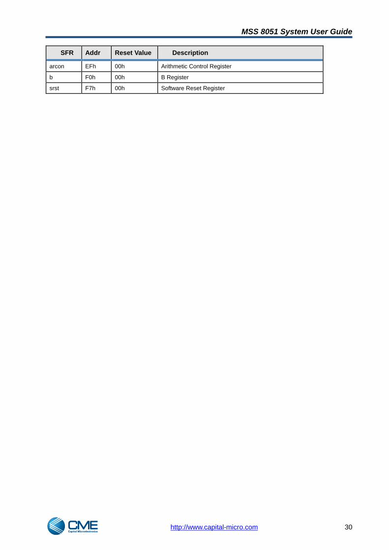
4.2 SFR reset values
Following table shows reset values and simple description of the SFR.
Table 4-3 SFR description and reset values
SFR Addr Reset Value Description
p0 80h FFh Port 0
sp 81h 07h Stack Pointer
dpl 82h 00h Data Pointer Low
dph 83h 00h Data Pointer High
wdtrel 86h 00h Watchdog Timer Reload register
pcon 87h 00h Power Control
tcon 88h 00h Timer/Counter Control Register
tmod 89h 00h Timer Mode Register
tl0 8Ah 00h Timer 0, low byte

MSS 8051 System User Guide
http://www.capital-micro.com 28
SFR Addr Reset Value Description
tl1 8Bh 00h Timer 1, low byte
th0 8Ch 00h Timer 0, high byte
th1 8Dh 00h Timer 1, high byte
ckcon 8Eh 71h Clock Control Register
p1 90h FFh Port 1
dps 92h 00h Data Pointer Select Register
dpc 93h 00h Data Pointer Control Register
pagesel 94h 01h Program Memory Page selector
d_pagesel 95h 01h External Data Memory Page selector
s0con 98h 00h Serial Port 0, Control Register
s0buf 99h 00h Serial Port 0, Data Buffer
ien2 9Ah 00h Interrupt Enable Register 2
s1con 9Bh 00h Serial Port 1, Control Register
s1buf 9Ch 00h Serial Port 1, Data Buffer
s1rell 9Dh 00h Serial Port 1, Reload Register, low byte
p2 A0h FFh Port 2
dmas0 A1h 00h DMA Source Address Register 0
dmas1 A2h 00h DMA Source Address Register 1
dmas2 A3h 00h DMA Source Address Register 2
dmat0 A4h 00h DMA Target Address Register 0
dmat1 A5h 00h DMA Target Address Register 1
dmat2 A6h 00h DMA Target Address Register 2
ien0 A8h 00h Interrupt Enable Register 0
ip0 A9h 00h Interrupt Priority Register 0
s0rell AAh D9h Serial Port 0, Reload Register, low byte
p3 B0h FFh Port 3
dmac0 B1h 00h DMA Byte Counter Register 0
dmac1 B2h 00h DMA Byte Counter Register 1
dmac2 B3h 00h DMA Byte Counter Register 2
dmasel B4h 00h DMA Channel Select Register
dmam0 B5h 00h DMA Mode Register 0
dmam1 B6h 1Fh DMA Mode Register 1
ip/ien1 B8h 00h Interrupt Priority Register / Enable Register 1
ip1 B9h 00h Interrupt Priority Register 1
s0relh BAh 03h Serial Port 0, Reload Register, high byte
s1relh BBh 03h Serial Port 1, Reload Register, high byte
ircon2 BFh 00h Interrupt Request Control 2 Register
ircon C0h 00h Interrupt Request Control Register
MSS 8051 System User Guide
http://www.capital-micro.com 29
SFR Addr Reset Value Description
ccen C1h 00h Compare/Capture Enable Register
ccl1 C2h 00h Compare/Capture Register 1, low byte
cch1 C3h 00h Compare/Capture Register 1, high byte
ccl2 C4h 00h Compare/Capture Register 2, low byte
cch2 C5h 00h Compare/Capture Register 2, high byte
ccl3 C6h 00h Compare/Capture Register 3, low byte
cch3 C7h 00h Compare/Capture Register 3, high byte
t2con C8h 00h Timer 2 Control Register
crcl CAh 00h Compare/Reload/Capture Register, low byte
crch CBh 00h Compare/Reload/Capture Register, high byte
tl2 CCh 00h Timer 2, low byte
th2 CDh 00h Timer 2, high byte
rtcsel CEh 00h RTC Select Register (address port to RTC)
rtcdat CFh 00h RTC Data Register (data port to RTC)
psw D0h 00h Program Status Word
adcon D8h 00h Serial Port 0 Baud Rate Select register (only adcon.7 bit used)
ien4 D1h 00h Interrupt Enable Register 4
i2c2dat D2h 00h Secondary I2C Data Register
i2c2adr D3h 00h Secondary I2C Address Register
i2c2con D4h 00h Secondary I2C Control Register
i2c2sta D5h F8h Secondary I2C Status Register
smb2_sel D6h 00h Secondary I2C SMBus Select Register
smb2_dst D7h 00h Secondary I2C SMBus Destination Register
i2cdat DAh 00h I2C Data Register
i2cadr DBh 00h I2C Address Register
i2ccon DCh 00h I2C Control Register
i2csta DDh F8h I2C Status Register
smb_sel DEh 00h I2C SMBus Select Register
smb_dst DFh 00h I2C SMBus Destination Register
acc E0h 00h Accumulator
spsta E1h 00h Serial Peripheral Status Register
spcon E2h 14h Serial Peripheral Control Register
spdat E3h 00h Serial Peripheral Data Register
spssn E4h FFh Serial Peripheral Slave Select Register
md0 E9h 00h Multiplication/Division Register 0
md1 EAh 00h Multiplication/Division Register 1
md2 EBh 00h Multiplication/Division Register 2
md3 ECh 00h Multiplication/Division Register 3
md4 EDh 00h Multiplication/Division Register 4
md5 EEh 00h Multiplication/Division Register 5
MSS 8051 System User Guide
http://www.capital-micro.com 30
SFR Addr Reset Value Description
arcon EFh 00h Arithmetic Control Register
b F0h 00h B Register
srst F7h 00h Software Reset Register

MSS 8051 System User Guide
http://www.capital-micro.com 31
4.3 SFR Description
(1) Accumulator - ACC
Accumulator is used by most of the 8051 instructions to hold the operand and to store the result of an operation. The mnemonics for accumulator-specific instructions refer to accumulator as A, not ACC.
(2) B Register - B
The B register is used during multiplying and division instructions. It can also be used as a scratch-pad register to hold temporary data.
(3) Program Status Word Register - PSW
The PSW register contains status bits that reflect the current state of the CPU. Note that the Parity bit can only be modified by hardware upon the state of ACC register.
Table 4-4 PSW Register
Bit Symbol Description Type
psw.7 cy Carry flag
R/W Carry bit in arithmetic operations and accumulator for Boolean operations.
psw.6 ac Auxiliary Carry flag
R/W Set if there is a carry-out from 3rd bit of Accumulator in BCD Operations
psw.5 f0 General purpose Flag 0
R/W General purpose flag available for user
psw.4 rs1 Register bank select control bit 1, used to select working register bank R/W
psw.3 rs0 Register bank select control bit 0, used to select working register bank R/W
psw.2 ov Overflow flag
R/W Set in case of overflow in Accumulator during arithmetic operations
psw.1 f1 General purpose Flag 1
R/W General purpose flag available for user.
psw.0 p
Parity flag
R Reflects the number of ‗1‘s in the Accumulator.
P = ‗1‘ if Accumulator contains an odd number of ‗1‘s
P = ‗0‘ if Accumulator contains an even number of ‗1‘s
The state of rs1 and rs0 bits selects the working register bank as follows:
Table 4-5 Register bank locations
rs1 rs0 Selected Register Bank Location
0 0 Bank 0 (00H – 07H)
0 1 Bank 1 (08H – 0FH)
1 0 Bank 2 (10H – 17H)
1 1 Bank 3 (18H – 1FH)
MSS 8051 System User Guide
http://www.capital-micro.com 32
(4) Stack Pointer – SP
This register points to the top of stack in internal data memory space. It is used to store the return address of program before executing interrupt routine or subprograms. The SP is incremented before executing PUSH or CALL instruction and it is decremented after executing POP or RET(I) instruction (it always points the top of stack).
(5) Data Pointer – DPH, DPL
One of 1, 2 or 8 (depending on core configuration) Data Pointer Registers can be accessed through DPL and DPH. The actual Data Pointer is selected by DPSEL register. These registers are intended to hold 16-bit address in the indirect addressing mode used by MOVX (move external memory), MOVC (move program memory) or JMP (computed branch) instructions. They may be manipulated as 16-bit register or as two separate 8-bit registers. DPH holds higher byte and DPL holds lower byte of indirect address. It is generally used to access external code or data space (e.g. MOVC A,@A+DPTR or MOV A,@DPTR respectively). It is generally used to access external code or data space, e.g.:
MOVC A,@A+DPTR (code space) MOV A,@DPTR (data space)
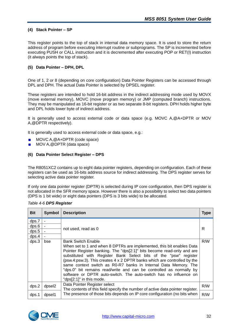
(6) Data Pointer Select Register – DPS
The R8051XC2 contains up to eight data pointer registers, depending on configuration. Each of these registers can be used as 16-bits address source for indirect addressing. The DPS register serves for selecting active data pointer register. If only one data pointer register (DPTR) is selected during IP core configuration, then DPS register is not allocated in the SFR memory space. However there is also a possibility to select two data pointers (DPS is 1 bit wide) or eight data pointers (DPS is 3 bits wide) to be allocated.
Table 4-6 DPS Register
Bit Symbol Description Type
dps.7 -
not used, read as 0 R dps.6 -
dps.5 -
dps.4 -
dps.3 bse Bank Switch Enable When set to 1 and when 8 DPTRs are implemented, this bit enables Data Pointer Register banking. The "dps[2:1]" bits become read-only and are substituted with Register Bank Select bits of the "psw" register (psw.4:psw.3). This creates 4 x 2 DPTR banks which are controlled by the same context switch as R0-R7 banks in Internal Data Memory. The "dps.0" bit remains read/write and can be controlled as normally by software or DPTR auto-switch. The auto-switch has no influence on "dps[2:1]" in this mode.
R/W
dps.2 dpsel2 Data Pointer Register select The contents of this field specify the number of active data pointer register. The presence of those bits depends on IP core configuration (no bits when
R/W
dps.1 dpsel1 R/W
MSS 8051 System User Guide
http://www.capital-micro.com 33
Bit Symbol Description Type
dps.0 dpsel0 only one DPTR selected, 1 dpsel0 bit when two DPTSs, or all three dpsel bits when 8 DPTRs selected)
R/W
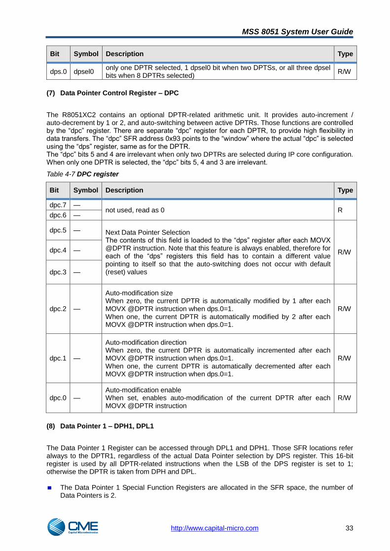
(7) Data Pointer Control Register – DPC
The R8051XC2 contains an optional DPTR-related arithmetic unit. It provides auto-increment / auto-decrement by 1 or 2, and auto-switching between active DPTRs. Those functions are controlled by the ―dpc‖ register. There are separate ―dpc‖ register for each DPTR, to provide high flexibility in data transfers. The ―dpc‖ SFR address 0x93 points to the ―window‖ where the actual ―dpc‖ is selected using the ―dps‖ register, same as for the DPTR. The ―dpc‖ bits 5 and 4 are irrelevant when only two DPTRs are selected during IP core configuration. When only one DPTR is selected, the ―dpc‖ bits 5, 4 and 3 are irrelevant.
Table 4-7 DPC register
Bit Symbol Description Type
dpc.7 — not used, read as 0 R
dpc.6 —
dpc.5 — Next Data Pointer Selection The contents of this field is loaded to the ―dps‖ register after each MOVX @DPTR instruction. Note that this feature is always enabled, therefore for each of the ―dps‖ registers this field has to contain a different value pointing to itself so that the auto-switching does not occur with default (reset) values
R/W dpc.4 —
dpc.3 —
dpc.2 —
Auto-modification size When zero, the current DPTR is automatically modified by 1 after each MOVX @DPTR instruction when dps.0=1. When one, the current DPTR is automatically modified by 2 after each MOVX @DPTR instruction when dps.0=1.
R/W
dpc.1 —
Auto-modification direction When zero, the current DPTR is automatically incremented after each MOVX @DPTR instruction when dps.0=1. When one, the current DPTR is automatically decremented after each MOVX @DPTR instruction when dps.0=1.
R/W
dpc.0 — Auto-modification enable When set, enables auto-modification of the current DPTR after each MOVX @DPTR instruction
R/W
(8) Data Pointer 1 – DPH1, DPL1
The Data Pointer 1 Register can be accessed through DPL1 and DPH1. Those SFR locations refer always to the DPTR1, regardless of the actual Data Pointer selection by DPS register. This 16-bit register is used by all DPTR-related instructions when the LSB of the DPS register is set to 1; otherwise the DPTR is taken from DPH and DPL.
The Data Pointer 1 Special Function Registers are allocated in the SFR space, the number of Data Pointers is 2.
MSS 8051 System User Guide
http://www.capital-micro.com 34
(9) Ports – P0, P1, P2, P3
After write operation, the contents of these registers can be observed at the corresponding pins of the chip (port 0, port 1, port2, port3). Writing a ‗1‘ to any of the port bits causes the corresponding pin to be at high level, and writing a ‗0‘ causes the corresponding pin to be held at low level. In case of reading, the state of P0, P1, P2, P3 registers reflects the value of the corresponding R8051XC2 port. It should be remembered that some of R8051XC2 instructions (the Read-Modify-Write instructions) while referring to the Port N in fact refer to the Port N register (e.g. INC P0; ANL P2, A) while the others refer directly to the external port input (e.g. MOV A, P1). The P0, P1, P2 and P3 registers are allocated in the SFR memory space when Port 0, Port 1, Port 2 or Port3 respectively are selected during IP core configuration.
(10) Program Memory Page Selector – PAGESEL
This register provides an additional address for program memory in banking scheme. Note that the default value is 1, to provide normal address generation (logical address of 8000h equals the physical address) when the ―pagesel‖ register is not written at all after reset. The value of 0 should not be used since it causes the banked area (logical address between 8000h-FFFFh) to overlap physically with the common bank (0000h-7FFFh).
(11) Data Memory Page Selector – D_PAGESEL
This register provides an additional address for data memory in banking scheme. Note that the default value is 1, to provide normal address generation (logical address of 8000h equals the physical address) when the ―d_pagesel‖ register is not written at all after reset. The value of 0 should not be used since it causes the banked area (logical address between 8000h-FFFFh) to overlap physically with the common bank (0000h-7FFFh).
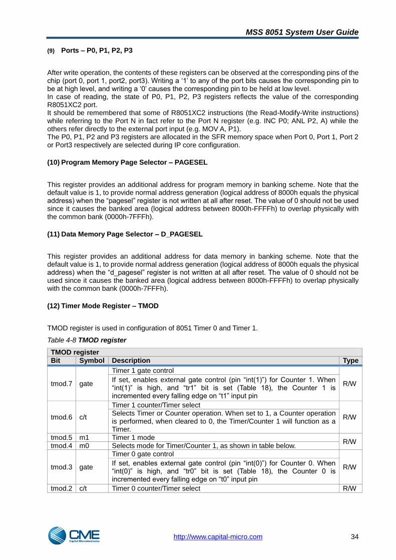
(12) Timer Mode Register – TMOD
TMOD register is used in configuration of 8051 Timer 0 and Timer 1.
Table 4-8 TMOD register
TMOD register Bit Symbol Description Type
tmod.7 gate
Timer 1 gate control
R/W If set, enables external gate control (pin ―int(1)‖) for Counter 1. When ―int(1)‖ is high, and ―tr1‖ bit is set (Table 18), the Counter 1 is incremented every falling edge on ―t1‖ input pin
tmod.6 c/t
Timer 1 counter/Timer select
R/W Selects Timer or Counter operation. When set to 1, a Counter operation is performed, when cleared to 0, the Timer/Counter 1 will function as a Timer.
tmod.5 m1 Timer 1 mode R/W
tmod.4 m0 Selects mode for Timer/Counter 1, as shown in table below.
tmod.3 gate
Timer 0 gate control
R/W If set, enables external gate control (pin ―int(0)‖) for Counter 0. When ―int(0)‖ is high, and ―tr0‖ bit is set (Table 18), the Counter 0 is incremented every falling edge on ―t0‖ input pin
tmod.2 c/t Timer 0 counter/Timer select R/W

MSS 8051 System User Guide
http://www.capital-micro.com 35
TMOD register Bit Symbol Description Type
Selects Timer or Counter operation. When set to 1, a Counter operation is performed, when cleared to 0, the Timer/Counter 0 will function as a Timer.
tmod.1 m1 Timer 0 mode R/W
tmod.0 m0 Selects mode for Timer/Counter 0, as shown in table below. Table 4-9 Timers/Counters modes
m0 m1 Mode Function
0 0 Mode 0 13-bit Counter/Timer, with 5 lower bits in tl0 (tl1) register and 8 bits in th0 (th1) register (for Timer 0 or Timer 1, respectively). Note, that unlike in 80C51, the 3 high-order bits of tl0 (tl1) are zeroed whenever Mode 0 is enabled.
0 1 Mode 1 16-bit Counter/Timer.
1 0 Mode 2 8 -bit auto-reload Counter/Timer. The reload value is kept in th0 (th1), while tl0 (tl1) is incremented every machine cycle. When tl0 (tl1) overflows, a value from th0 (th1) is copied to tl0 (tl1).
1 1 Mode 3
For Timer1: Timer1 is stopped.
For Timer0: Timer 0 acts as two independent 8 bit Timers / Counters – tl0, th0.
- tl0 uses the Timer0 control bits and sets tf0 flag on overflow
- th0 operates as Timer. It is enabled by tr1 bit and sets tf1 flag on overflow.
(13) Timer/Counter Control Register – TCON
TCON register reflects the current status of 8051 Timer 0 and Timer 1 and it is used to control operation of these modules.
Table 4-10 TCON register
TCON register
Bit Symbol Description Type
tcon.7 tf1
Timer 1 overflow flag
R/W Bit set by hardware when Timer1 overflows. This flag can be cleared by software and is automatically cleared when interrupt is processed.
tcon.6 tr1 Timer1 Run control
R/W If cleared, Timer 1 stops.
tcon.5 tf0
Timer 0 overflow flag
R/W Bit set by hardware when Timer 0 overflows. This flag can be cleared by software and is automatically cleared when interrupt is processed.
tcon.4 tr0 Timer 0 Run control
R/W If cleared, Timer 0 stops.
tcon.3 ie1 External interrupt 1 flag
R/W Set by hardware, when external interrupt int1 (edge/level, depending on settings) is observed. Cleared by hardware when interrupt is processed.
tcon.2 it1 External interrupt 1 type control
R/W If set, external interrupt 1 is activated at falling edge on input pin. If cleared, external interrupt 1 is activated at low level on input pin.
tcon.1 ie0 External interrupt 0 flag
R/W Set by hardware, when external interrupt int0 (edge/level, depending on settings) is observed. Cleared by hardware when interrupt is processed.
tcon.0 it0 External interrupt 0 type control
R/W If set, external interrupt 0 is activated at falling edge on input pin. If cleared, external interrupt 0 is activated at low level on input pin.

MSS 8051 System User Guide
http://www.capital-micro.com 36
The tf0, tf1 (timer 0 and timer 1 overflow flags), ie1 and ie1 (external interrupt 0 and 1 flags) will be automatically cleared by hardware when the corresponding service routine is called.
(14) Timer Mode Register – TMOD
TMOD register is used in configuration of R8051XC2 Timer 0 and Timer1. TMOD register is allocated in the SFR memory space when Timer 0 or Timer 1 is selected during IP core configuration.
Table 4-11 TMOD Register
Bit Symbol Description Type
tmod.7 gate
Timer 1 gate control If set, enables external gate control (pin ―int(1)‖) for Counter 1. When ―int(1)‖ is high, and ―tr1‖ bit is set (Table 18), the Counter 1 is incremented every falling edge on ―t1‖ input pin
R/W
tmod.6 c/t
Timer 1 counter/timer select Selects Timer or Counter operation. When set to 1, a Counter operation is performed, when cleared to 0, the Timer/Counter 1 will function as a Timer.
R/W
tmod.5 m1 Timer 1 mode Selects mode for Timer/Counter 1, as shown in table below.
R/W
tmod.4 m0
tmod.3 gate
Timer 0 gate control If set, enables external gate control (pin ―int(0)‖) for Counter 0. When ―int(0)‖ is high, and ―tr0‖ bit is set (Table 18), the Counter 0 is incremented every falling edge on ―t0‖ input pin
R/W
tmod.2 c/t
Timer 0 counter/timer select Selects Timer or Counter operation. When set to 1, a Counter operation is performed, when cleared to 0, the Timer/Counter 0 will function as a Timer.
R/W
tmod.1 m1 Timer 0 mode Selects mode for Timer/Counter 0, as shown in table below.
R/W
tmod.0 m0
Table 4-12 Timers/Counters Modes
m0 m1 Mode Function
0 0 Mode 0 13-bit Counter/Timer, with 5 lower bits in tl0 (tl1) register and 8 bits in th0 (th1) register (for Timer 0 or Timer 1, respectively). Note, that unlike in 80C51, the 3 high-order bits of tl0 (tl1) are zeroed whenever Mode 0 is enabled.
0 1 Mode 1 16-bit Counter/Timer.
1 0 Mode 2 8 -bit auto-reload Counter/Timer. The reload value is kept in th0 (th1), while tl0 (tl1) is incremented every machine cycle. When tl0 (tl1) overflows, a value from th0 (th1) is copied to tl0 (tl1).
1 1 Mode 3
For Timer1: Timer1 is stopped. For Timer0: Timer 0 acts as two independent 8 bit Timers / Counters – tl0, th0. - tl0 uses the Timer0 control bits and sets tf0 flag on overflow - th0 operates as timer. It is enabled by tr1 bit and sets tf1 flag on overflow.

MSS 8051 System User Guide
http://www.capital-micro.com 37
(15) Timer0 – TH0, TL0
These registers reflect the state of Timer 0. TH0 holds higher byte and TL0 holds lower byte. Timer 0 can be configured to operate as either timer or counter. TL0 and TH0 registers are allocated in the SFR memory space when Timer 0 is selected during IP core configuration.
(16) Timer1 – TH1, TL1
These registers reflect the state of Timer 1. TH1 holds higher byte and TL1 holds lower byte. Timer 1 can be configured to operate as either timer or counter. TL1 and TH1 registers are allocated in the SFR memory space when Timer 1 is selected during IP core configuration.
(17) Timer 2 Control Register – T2CON
T2CON register reflects the current status of R8051XC2 Timer 2 and it is used to control Timer 2 operation. T2CON register is allocated in the SFR memory space when Timer 2 is selected during IP core configuration.
Table 4-13 T2CON Register
Bit Symbol Description Type
t2con.7 t2ps Prescaler select t2ps = 0 – timer 2 is clocked with 1/12 of the oscillator frequency. t2ps = 1 – timer 2 is clocked with 1/24 of the oscillator frequency.
R/W
t2con.6 i3fr Active edge selection for external interrupt ―int3‖, (used also as compare and capture signal) 0 - falling edge 1 - rising edge
R/W
t2con.5 i2fr Active edge selection for external interrupt ―int2‖ 0 - falling edge 1 - rising edge
R/W
t2con.4 t2r1 Timer 2 reload mode selection: 0X – reload disabled 10 – Mode 0 11 – Mode 1
R/W t2con.3 t2r0
t2con.2 t2cm
Timer 2 compare mode selection
R/W 0 – Mode 0
1 – Mode 1
t2con.1 t2i1
Timer 2 input selection: (t2i1, t2i0) 00 timer 2 stopped 01 input frequency f/12 or f/24 10 timer 2 is incremented by falling edge detection at pin ―t2‖ 11 input frequency f/12 or f/24 gated by external pin ―t2‖
R/W
(18) Timer 2 – TH2, TL2
These registers reflect the state of Timer 2. TH2 holds higher byte and TL2 holds lower byte.

MSS 8051 System User Guide
http://www.capital-micro.com 38
Timer 2 can be configured to operate in compare, capture or reload modes. TL2 and TH2 registers are allocated in the SFR memory space when Timer 2 is selected during IP core configuration.
(19) Compare/Capture Enable Register – CCEN
CCEN register serves as a configuration register for Compare/Capture Unit associated with the Timer 2 (more description see 6H0).
Table 4-14 CCEN register
Bit Symbol Description Type
ccen.7 cocah3 compare/capture mode for CC3 register R/W
ccen.6 cocal3 cocah3 cocal3 Description R/W
0 0 compare/capture disabled
0 1 capture on rising edge at pin cc0
1 0 compare enabled
1 1 capture on write operation into register cc3
ccen.5 cocah2 compare/capture mode for CC2 register R/W
ccen.4 cocal2 cocah2 cocal2 Description R/W
0 0 compare/capture disabled
0 1 capture on rising edge at pin cc1
1 0 compare enabled
1 1 capture on write operation into register ccl2
ccen.3 cocah1 compare/capture mode for CC1 register R/W
ccen.2 cocal1 cocah1 cocal1 Description R/W
0 0 compare/capture disabled
0 1 capture on rising edge at pin cc2
1 0 compare enabled
1 1 capture on write operation into register cc1
ccen.1 cocah0 compare/capture mode for CRC register R/W
ccen.0 cocal0 cocah0 cocal0 Description R/W
0 0 compare/capture disabled
0 1 capture on falling/rising edge at pin cc3
1 0 compare enabled
1 1 capture on write operation into register crcl
(20) Compare/Capture Registers – CC1, CC2, CC3
Compare/Capture Registers (CC1, CC2, and CC3) are 16-bit registers used in the operation of Compare/Capture Unit associated with the Timer 2 (more description see 7H0 ). CCHn holds higher byte and CCLn holds lower byte of the CCn register.
CCL1, CCH1, CCL2, CCH2, CCL3, CCH3 are allocated in SFR memory space.
(21) Compare/Reload/Capture Register – CRCH, CRCL
Compare/Reload/Capture Register CRC is a 16-bit wide register used in the operation of Compare/Capture Unit associated with Timer 2 (more description see 0). CRCH holds higher byte and CRCL holds lower byte.
MSS 8051 System User Guide
http://www.capital-micro.com 39
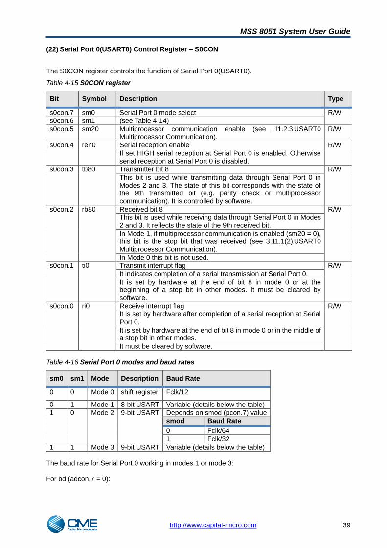
(22) Serial Port 0(USART0) Control Register – S0CON
The S0CON register controls the function of Serial Port 0(USART0).
Table 4-15 S0CON register
Bit Symbol Description Type
s0con.7 sm0 Serial Port 0 mode select R/W
s0con.6 sm1 (see Table 4-14)
s0con.5 sm20 Multiprocessor communication enable (see 46H11.2.347HUSART0 Multiprocessor Communication).
R/W
s0con.4 ren0 Serial reception enable R/W
If set HIGH serial reception at Serial Port 0 is enabled. Otherwise serial reception at Serial Port 0 is disabled.
s0con.3 tb80 Transmitter bit 8 R/W
This bit is used while transmitting data through Serial Port 0 in Modes 2 and 3. The state of this bit corresponds with the state of the 9th transmitted bit (e.g. parity check or multiprocessor communication). It is controlled by software.
s0con.2 rb80 Received bit 8 R/W
This bit is used while receiving data through Serial Port 0 in Modes 2 and 3. It reflects the state of the 9th received bit.
In Mode 1, if multiprocessor communication is enabled (sm20 = 0), this bit is the stop bit that was received (see 3.11.1(2)48HUSART0 Multiprocessor Communication).
In Mode 0 this bit is not used.
s0con.1 ti0 Transmit interrupt flag R/W
It indicates completion of a serial transmission at Serial Port 0.
It is set by hardware at the end of bit 8 in mode 0 or at the beginning of a stop bit in other modes. It must be cleared by software.
s0con.0 ri0 Receive interrupt flag R/W
It is set by hardware after completion of a serial reception at Serial Port 0.
It is set by hardware at the end of bit 8 in mode 0 or in the middle of a stop bit in other modes.
It must be cleared by software.
Table 4-16 Serial Port 0 modes and baud rates
sm0 sm1 Mode Description Baud Rate
0 0 Mode 0 shift register Fclk/12
0 1 Mode 1 8-bit USART Variable (details below the table)
1 0 Mode 2 9-bit USART Depends on smod (pcon.7) value
smod Baud Rate
0 Fclk/64
1 Fclk/32
1 1 Mode 3 9-bit USART Variable (details below the table)
The baud rate for Serial Port 0 working in modes 1 or mode 3: For bd (adcon.7 = 0):

MSS 8051 System User Guide
http://www.capital-micro.com 40
baud rate = 2SMOD*Fclk
32*(Timer1 overflow rate)
For bd (adcon.7 = 1):
baud rate = 2SMOD*Fclk
64*(210 – s0rel)
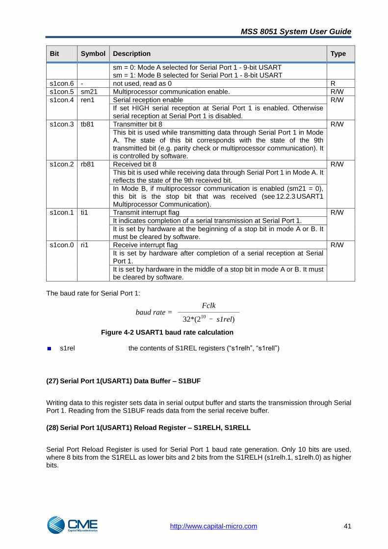
Figure 4-1 USART0 baud rate calculation
smod (pcon.7) Serial Port 0 baud rate select flag
s0rel the contents of S0REL registers (s0relh, s0rell) bd (adcon.7) the MSB of ―adcon‖ register
(23) Serial Port 0(USART0) Data Buffer – S0BUF
Writing data to this register sets data in serial output buffer and starts the transmission through Serial Port 0. Reading from the S0BUF, reads data from the serial receive buffer.
(24) Serial Port 0(USART0) Reload Register – S0RELH, S0RELL
Serial Port 0 Reload Register is used for Serial Port 0 baud rate generation. Only 10 bits are used, where 8 bits from the S0RELL as lower bits and 2 bits from the S0RELH (s0relh.1, s0relh.0) as higher bits.
(25) Serial Port 0 Baud Rate Select register – ADCON
The MSB of this register is used by Serial Port 0 for baud rate generation.
Table 4-17 ADCON register
Bit Symbol Description Type
adcon.7 bd Serial Port 0 baud rate select (in modes 1 and 3) R/W
When 1, additional internal baud rate generator is used, otherwise Timer 1 overflow is used
adcon.6 - not used, read as 0 R
adcon.5 -
adcon.4 -
adcon.3 -
adcon.2 -
adcon.1 -
adcon.0 -
(26) Serial Port 1 (USART1) Control Register – S1CON
The S1CON register controls the function of the Serial Port 1.
Table 4-18 S1CON register
Bit Symbol Description Type
s1con.7 sm Serial Port 1 mode select R/W
MSS 8051 System User Guide
http://www.capital-micro.com 41
Bit Symbol Description Type
sm = 0: Mode A selected for Serial Port 1 - 9-bit USART sm = 1: Mode B selected for Serial Port 1 - 8-bit USART
s1con.6 - not used, read as 0 R
s1con.5 sm21 Multiprocessor communication enable. R/W
s1con.4 ren1 Serial reception enable R/W
If set HIGH serial reception at Serial Port 1 is enabled. Otherwise serial reception at Serial Port 1 is disabled.
s1con.3 tb81 Transmitter bit 8 R/W
This bit is used while transmitting data through Serial Port 1 in Mode A. The state of this bit corresponds with the state of the 9th transmitted bit (e.g. parity check or multiprocessor communication). It is controlled by software.
s1con.2 rb81 Received bit 8 R/W
This bit is used while receiving data through Serial Port 1 in Mode A. It reflects the state of the 9th received bit.
In Mode B, if multiprocessor communication is enabled (sm21 = 0), this bit is the stop bit that was received (see 52H12.2.353HUSART1 Multiprocessor Communication).
s1con.1 ti1 Transmit interrupt flag R/W
It indicates completion of a serial transmission at Serial Port 1.
It is set by hardware at the beginning of a stop bit in mode A or B. It must be cleared by software.
s1con.0 ri1 Receive interrupt flag R/W
It is set by hardware after completion of a serial reception at Serial Port 1.
It is set by hardware in the middle of a stop bit in mode A or B. It must be cleared by software.
The baud rate for Serial Port 1:
baud rate = Fclk
32*(210 – s1rel)
Figure 4-2 USART1 baud rate calculation
s1rel the contents of S1REL registers (―s1relh‖, ―s1rell‖)
(27) Serial Port 1(USART1) Data Buffer – S1BUF
Writing data to this register sets data in serial output buffer and starts the transmission through Serial Port 1. Reading from the S1BUF reads data from the serial receive buffer.
(28) Serial Port 1(USART1) Reload Register – S1RELH, S1RELL
Serial Port Reload Register is used for Serial Port 1 baud rate generation. Only 10 bits are used, where 8 bits from the S1RELL as lower bits and 2 bits from the S1RELH (s1relh.1, s1relh.0) as higher bits.

MSS 8051 System User Guide
http://www.capital-micro.com 42
(29) Watchdog Timer – WDTREL
WDTREL register holds the reload value of 7 high-order bits of the Watchdog Timer (5.9). It also configures the frequency prescaller for the Watchdog Timer. WDTREL register is allocated in the SFR memory space when Watchdog Timer is selected during IP core configuration.
Table 4-19 WDTEL register
Timer 2 Control Register – T2CON
Bit Symbol Description Type
wdtrel.6 wdtrel.5 wdtrel.4 wdtrel.3 wdtrel.2 wdtrel.1 wdtrel.0
Watchdog reload value Reload value for the highest 7 bits of the watchdog timer. This value is loaded to the Watchdog Timer when a refresh is triggered by a consecutive setting of bits wdt (ien0.6) and swdt (ien1.6). For details see Watchdog Timer description (5.9).
R/W
(30) Interrupt Enable 0 Register – IEN0
The external interrupt enable flags are implemented. The Watchdog Timer Refresh Flag is implemented. The Timer 0 interrupt enable flag is implemented. The Timer 1 interrupt enable flag is implemented. The Timer 2 interrupt enable flag is implemented. The Serial Port 0 interrupt enable flag is implemented.
MSS 8051 System User Guide
http://www.capital-micro.com 43
Table 4-20 IEN0 register
Bit Symbol Description Type
ien0.7 eal
Interrupts enable
R/W When set to 0 – all interrupts are disabled Otherwise enabling each interrupt is done by setting the corresponding interrupt enable bit
ien0.6 wdt
Watchdog Timer refresh flag
R/W
Set to initiate a refresh of the watchdog Timer. Must be set directly before swdt (ien1.6) is set to prevent an unintentional refresh of the watchdog Timer. The wdt bit is cleared by hardware after the next instruction executed after the one that had set this bit, so that watchdog refresh can be done only with direct sequence of setting wdt and swdt.
ien0.5 et2
Timer 2 interrupt enable
R/W When et2=0 Timer 2 interrupt is disabled. When et2=1 and eal=1 Timer 2 interrupt is enabled.
ien0.4 es0 Serial Port 0 interrupt enable
R/W When es0=0 Serial Port 0 interrupt is disabled. When es0=1 and eal=1 Serial Port 0 interrupt is enabled.
ien0.3 et1
Timer 1 overflow interrupt enable
R/W When et1=0 Timer 0 overflow interrupt is disabled. When et1=1 and eal=1 Timer 1 overflow interrupt is enabled.
ien0.2 ex1 External interrupt 1 enable
R/W When ex1=0 external interrupt 1 is disabled. When ex1=1 and eal=1 external interrupt 1 is enabled.
ien0.1 et0 Timer 0 overflow interrupt enable
R/W When et0=0 Timer 0 overflow interrupt is disabled. When et0=1 and eal=1 Timer 0 overflow interrupt is enabled.
ien0.0 ex0
External interrupt 0 enable
R/W When ex0=0 external interrupt 0 is disabled. When ex0=1 and eal=1 external interrupt 0 is enabled.
(31) Interrupt Enable 1 Register – IEN1
The external interrupt enable flags are implemented. The Timer 2 interrupt enable flag is implemented. The Watchdog Timer Start/Refresh Flag is implemented.
Table 4-21 IEN1 register
Bit Symbol Description Type
ien1.7 exen2
Timer 2 external reload interrupt enable
R/W When exen2=0, Timer 2 external reload interrupt 2 is disabled. When exen2=1 and eal=1, Timer 2 external reload interrupt 2 is enabled.
ien1.6 swdt
Watchdog Timer start/refresh flag.
R/W Set to activate/refresh the watchdog Timer. When set directly after setting wdt (ien0.6), a watchdog Timer refresh is performed. This bit is immediately cleared by hardware.
ien1.5 ex6
External interrupt 6 enable
R/W When ex6=0 external interrupt 6 is disabled. When ex6=1 and eal=1 external interrupt 6 is enabled.
MSS 8051 System User Guide
http://www.capital-micro.com 44
Bit Symbol Description Type
ien1.4 ex5
External interrupt 5 enable
R/W When ex5=0 external interrupt 5 is disabled. When ex5=1 and eal=1 external interrupt 5 is enabled.
ien1.3 ex4
External interrupt 4 enable
R/W When ex4=0 external interrupt 4 is disabled. When ex4=1 and eal=1 external interrupt 4 is enabled.
ien1.2 ex3
External interrupt 3 enable
R/W When ex3=0 external interrupt 3 is disabled. When ex3=1 and eal=1 external interrupt 3 is enabled.
ien1.1 ex2
External interrupt 2 enable
R/W When ex2=0 external interrupt 2 is disabled. When ex2=1 and eal=1 external interrupt 2 is enabled.
ien1.0 ex7
External interrupt 7 enable
R/W When ex7=0 external interrupt 7 is disabled. When ex7=1 and eal=1 external interrupt 7 is enabled.
(32) Interrupt Enable 2 Register – IEN2
The Serial Port 1 interrupt enable flag is implemented.
Table 4-22 IEN2 register
Bit Symbol Description Type
ien2.7 - not used, read as 0 R
ien2.6 -
ien2.5 ex12 External interrupt 12 enable When ex12=0 external interrupt 12 is disabled. When ex12=1 and eal=1 external interrupt 12 is enabled.
R/W
ien2.4 ex11 External interrupt 11 enable When ex11=0 external interrupt 11 is disabled. When ex11=1 and eal=1 external interrupt 11 is enabled.
R/W
ien2.3 ex10 External interrupt 10 enable When ex10=0 external interrupt 10 is disabled. When ex10=1 and eal=1 external interrupt 10 is enabled.
R/W
ien2.2 ex9 External interrupt 9 enable When ex9=0 external interrupt 9 is disabled. When ex9=1 and eal=1 external interrupt 9 is enabled.
R/W
ien2.1 ex8 External interrupt 8 enable When ex8=0 external interrupt 8 is disabled. When ex8=1 and eal=1 external interrupt 8 is enabled.
R/W
ien2.0 es1 Serial Port 1 interrupt enable R/W When es1=0 Serial Port 1 interrupt is disabled.
When es1=1 and eal=1 Serial Port 1 interrupt is enabled.
(33) Interrupt Enable 2 Register – IEN4
The RTC interrupt enable flag is implemented.

MSS 8051 System User Guide
http://www.capital-micro.com 45
Table 4-23 IEN4 register
Bit Symbol Description Type
ien4.7 ien4.6
- -
not used, read as 0 R
ien4.5 ertc Real Time Clock interrupt enable When ertc=0 the RTC interrupt is disabled. When ertc=1 and eal=1 the RTC interrupt is enabled.
R/W
ien4.4 ien4.3 ien4.2 ien4.1 ien4.0
- R/W
(34) Interrupt Priority Registers – IP0, IP1
The 13 interrupt sources are grouped into 6 priority groups. For each of the groups, one of four priority levels can be selected. It is achieved by setting appropriate values in IP0 and IP1 registers. The contents of the Interrupt Priority Registers define the priority levels for each interrupt source according to the tables below.
The Watchdog Timer Status Flag is implemented.
Table 4-24 IP0 register
Bit Symbol Description Type
ip0.7 - not used, read as 0 R
ip0.6 wdts Watchdog Timer status flag R/W
Set by hardware when the watchdog Timer reset occurs.
ip0.5 - Interrupt priority R/W
ip0.4 - Each bit together with corresponding bit from IP1 register specifies the priority level of the respective interrupt priority group.
ip0.3 -
ip0.2 -
ip0.1 -
ip0.0 -
Table 4-25 IP1 register
Bit Symbol Description Type
ip1.7 - not used, read as 0 R
ip1.6 -
ip1.5 - Interrupt priority
R/W
ip1.4 -
Each bit together with corresponding bit from IP0 register specifies the priority level of the respective interrupt priority group.
ip1.3 -
ip1.2 -
ip1.1 -
ip1.0 -

MSS 8051 System User Guide
http://www.capital-micro.com 46
(35) Interrupt Request Control Register – IRCON
Table 4-26 IRCON register
Bit Symbol Description Type
ircon.7 exf2 Timer 2 external reload flag R/W
ircon.6 tf2 Timer 2 overflow flag R/W
ircon.5 iex6 External interrupt 6 edge flag R/W
ircon.4 iex5 External interrupt 5 edge flag R/W
ircon.3 iex4 External interrupt 4 edge flag R/W
ircon.2 iex3 External interrupt 3 edge flag R/W
ircon.1 iex2 External interrupt 2 edge flag R/W
ircon.0 iex7 External interrupt 7 edge flag R/W
(36) Power Control Register – PCON
The ―pmw‖ bit is implemented for Program Memory Write Mode.
Table 4-27 PCON register
Bit Symbol Description Type
pcon.7 smod Serial Port 0 baud rate select (see Table 4-14) (baud rate doubler) R/W
pcon.6 wdt_tm Watchdog Timer Test Mode flag R/W
When set to 1, the fclk/12 divider at the input of the Watchdog Timer is skipped
pcon.5 isr_tm Interrupt Service Routine Test Mode flag R/W
When set to 1, the interrupt vectors assigned to Timer 0 & 1, Serial Port 0 & 1, SPI and I2C interfaces can be triggered only with the use of external inputs of the core
pcon.4 pmw Program memory write mode R/W
Setting this bit enables the program memory write mode
pcon.3 p2sel High-order address byte configuration bit R/W
Chooses the higher byte of address (―memaddr[15:8]‖) during MOVX @Ri operations;
when 0, the ―memaddr[15:8]‖ = ―p2reg‖ when 1, the ―memaddr[15:8]‖ = ADDR_HIGH_RI
The ―p2reg‖ is the contents of Port2 output register. The ADDR_HIGH_RI = 8‘h0 is the parameter defined before synthesis.
pcon.2 gf0 General Purpose Flag R/W
pcon.1 stop Stop mode control R/W
Setting this bit activates the Stop Mode. This bit is always read as 0
pcon.0 idle Idle mode control R/W
Setting this bit activates the Idle Mode. This bit is always read as 0
(37) Clock Control Register – CKCON
The content of this register defines the number of internally generated wait states that occur during read/write accesses to external data and program memory.

MSS 8051 System User Guide
http://www.capital-micro.com 47
Table 4-28 CKCON register
Bit Symbol Description Type
ckcon.7 - not used, read as 0 R
ckcon.6 - Program memory wait state control R/W
ckcon.5 -
ckcon.4 -
ckcon.3 - not used, read as 0 R
ckcon.2 - External data memory stretch cycle control R/W
ckcon.1 -
ckcon.0 -
Table 4-29 program memory wait status cycle width
CKCON Register Wait Value
Read Signals Width Write Signals Width
ckcon.6 ckcon.5 ckcon.4 memaddr mempsrd memaddr mempsrd
0 0 0 0 1 1 2 1
0 0 1 1 2 2 3 1
0 1 0 2 3 3 4 2
0 1 1 3 4 4 5 3
1 1 0 4 5 5 6 4
1 0 1 5 6 6 7 5
1 1 0 6 7 7 8 6
1 1 1 7 8 8 9 7
Table 4-30 external data memory wait status cycle width
CKCON Register Strech Value
Read Signals Width Write Signals Width
ckcon.2 ckcon.1 ckcon.0 memaddr memrd memaddr memwr
0 0 0 0 1 1 2 1
0 0 1 1 2 2 3 1
0 1 0 2 3 3 4 2
0 1 1 3 4 4 5 3
1 0 0 4 5 5 6 4
1 0 1 5 6 6 7 5
1 1 0 6 7 7 8 6
1 1 1 7 8 8 9 7
(38) Arithmetic Control Register – ARCON
MD0: Address - E9H Reset value - 00H The ARCON register controls the operation of MDU and informs about its current state.
Table 4-31 ARCON register
Bit Symbol Description Type
arcon.7 mdef MDU Error flag MDEF R
Indicates an improperly performed operation (when one of the arithmetic operations has been restarted or interrupted by a new operation).
arcon.6 mdov MDU Overflow flag MDOV R
Overflow occurrence in the MDU operation.
arcon.5 slr Shift direction R/W
slr = 0 - shift left operation. slr = 1 - shift right operation.
arcon.4 sc.4 Shift counter R/W

MSS 8051 System User Guide
http://www.capital-micro.com 48
Bit Symbol Description Type
arcon.3 sc.3 When set to all ‗0‘s, normalize operation is selected. After normalization, the ―sc.0‖ … ―sc.4‖ contain the number of normalizing shifts performed.
arcon.2 sc.2
arcon.1 sc.1
arcon.0 sc.0 When at least one of these bit is set high shift operation is selected. The number of shifts performed is determined by the number written to ―sc.4‖.., ―sc.0‖, where ―sc.4‖ is the MSB.
(39) Multiplication/Division Registers – MD0, MD1, MD2, MD3, MD4, MD5
The MD0 … MD5 are registers used in the MDU operation. For detailed description of MDU functions refer to section 22H5 23H. MD0: Address - E9H Reset value - 00H MD1: Address - EAH Reset value - 00H MD2: Address - EBH Reset value - 00H MD3: Address - ECH Reset value - 00H MD4: Address - EDH Reset value - 00H MD5: Address - EEH Reset value - 00H
(40) I2C Data Register – I2CDAT
The I2CDAT register contains a byte to be transmitted through I2C bus or a byte which has just been received through I2C bus. The CPU can read from and write to this 8-bit, directly addressable SFR while it is not in the process of byte shifting. The I2CDAT register is not shadowed or double buffered so the user should only read I2CDAT when an I2C interrupt occurs. Detailed description of I2C interface functionality can be found in section 32H10 ―33HI2C‖.
(41) I2C Address Register – I2CADR
The I2CADR register holds the own address of 8051 I2C slave interface. This address is used to recognize if an external device is attempting to access the 8051 as slave via I2C bus. Detailed description of I2C interface functionality can be found in section 34H10 ―35HI2C‖.
Table 4-32 I2CADR register
Bit Symbol Description Type
i2cadr.7
adr Own I2C slave address (7 bit) R/W
i2cadr.6
i2cadr.5
i2cadr.4
i2cadr.3
i2cadr.2
i2cadr.1
i2cadr.0 gc
General Call Address Acknowledge
R/W If this bit is set, the general call address is recognized; otherwise it is ignored.
(42) I2C Control Register – I2CCON
The I2CCON register controls the operation of I2C interface. The CPU can read from and write to this
MSS 8051 System User Guide
http://www.capital-micro.com 49
8-bit, directly addressable SFR. Two bits of this register are affected by the I2C hardware: the si bit is set when serial interrupt is requested, and the ―sto‖ bit is cleared when STOP condition is present on the I2C bus. Detailed description of I2C interface functionality can be found in section 36H10 ―37HI2C‖. About clock rate setting, please refer to 38H(3).
Table 4-33 I2CCON register
Bit Symbol Description Type
i2ccon.7 cr2 Clock rate bit 2 R/W
i2ccon.6 ens1 I2C enable bit R/W
When ens1=‘0‘ the ―sdao‖ and ―sclo‖ outputs are set to 1, that drives the output pads of the chip in high impedance, and ―sdai‖ and ―scli‖ input signals are ignored.
When ens1=‘1‘ I2C component is enabled.
i2ccon.5 sta START Flag R/W
When sta=‘1‘, the I2C component checks the I
2C bus status and if the
bus is free a START condition is generated.
i2ccon.4 sto STOP Flag R/W
When sto=‘1‘ and I2C interface is in master mode, a STOP condition is
transmitted to the I2C bus.
i2ccon.3 si Serial Interrupt Flag R/W
The ―si ―is set by hardware when one of 25 out of 26 possible I2C states is entered (2.4.46 ). The only state that does not set the ―si‖ is state F8h, which indicates that no relevant state information is available. The ―si‖ flag must be cleared by software. In order to clear the ―si‖ bit, ‗0‘ must be written to this bit. Writing a ‗1‘ to si bit does not change value of the ―si‖.
i2ccon.2 aa Assert Acknowledge Flag R/W
When aa=‘1‘, an ―acknowledge‖ will be returned when: - the ―own slave address‖ has been received - the general call address has been received while gc bit in i2cadr register was set - a data byte has been received while I
2C was in master receiver mode
- a data byte has been received while I2C was in slave receiver mode
When aa=‘0‘, an ―not acknowledge‖ will be returned when: - a data byte has been received while I
2C was in master receiver mode
- a data byte has been received whileI2C was in slave receiver mode
i2ccon.1 cr1 Clock rate bit 1 R/W
i2ccon.0 cr0 Clock rate bit 0 R/W
(43) I2C Status Register – I2CSTA
The contents of this register reflect the actual state of I2C interface. Detailed description of I2C interface functionality can be found in section 39H10 ―40HI2C‖.
Table 4-34 I2CSTA register
Bit Symbol Description Type
i2csta.7 i2csta.6 i2csta.5 i2csta.4 i2csta.3
- I2CStatus Code R
i2csta.2 i2csta.1
- Not implemented, read as 0 R

MSS 8051 System User Guide
http://www.capital-micro.com 50
Bit Symbol Description Type
i2csta.0
(44) I2C SMBus Select Register – SMB_SEL
This register is used to enable the SMBus extension to the primary I2C interface and to provide a read/write access port to the SMBus timeout registers.
Table 4-35 SMB_SEL register
Bit Symbol Description Type
smb_sel.7 - SMBus Extension Enable R/W
smb_sel.6 smb_sel.5 smb_sel.4
Not implemented, read as 0 R
smb_sel.3 smb_sel.2 smb_sel.1 smb_sel.0
- SMBus Extension Enable SMBus Timeout Register Pointer Selects one of the Timeout Registers for read/write access through the SMB_DST register.
R/W
(45) I2C SMBus Destination Register – SMB_DST
This register is used to provide a read/write access port to the SMBus timeout registers. Data read or written to that register is actually read or written to the Timeout Register which is pointed by the SMB_SEL register.
(46) SPI Serial Peripheral Status Register – SPSTA
The SPSTA register contains flags to signal data transfer complete, Write collision and inconsistent logic level on ―ssn‖ (slave select) pin (mode fault error). Table 4-36 SPSTA register
Bit Symbol Description Type
spsta.7 spif
Serial Peripheral Data Transfer Flag
R Set by hardware upon data transfer completion.
Cleared by hardware when data transfer is in progress. Can be also cleared by reading the ―spsta‖ register with the ―spif‖ bit set, and then reading the ―spdat‖ register.
spsta.6 wcol
Write Collision Flag
R Set by hardware upon write collision to ―spdat‖.
Cleared by hardware upon data transfer completion when no collision has occurred. Can be also cleared by an access to ―spsta‖ register and an access to ―spdat‖ register.
spsta.5 sserr
Synchronous Serial Slave Error Flag
R Set by hardware when ―ssn‖ input is de-asserted before the end of receive sequence.
Cleared by disabling the SPI module (clearing ―spen‖ bit in ―spcon‖ register).
spsta.4 modf Mode Fault Flag
R Set by hardware when the ―ssn‖ pin level is in conflict with actual mode of the SPI controller (configured as master while externally
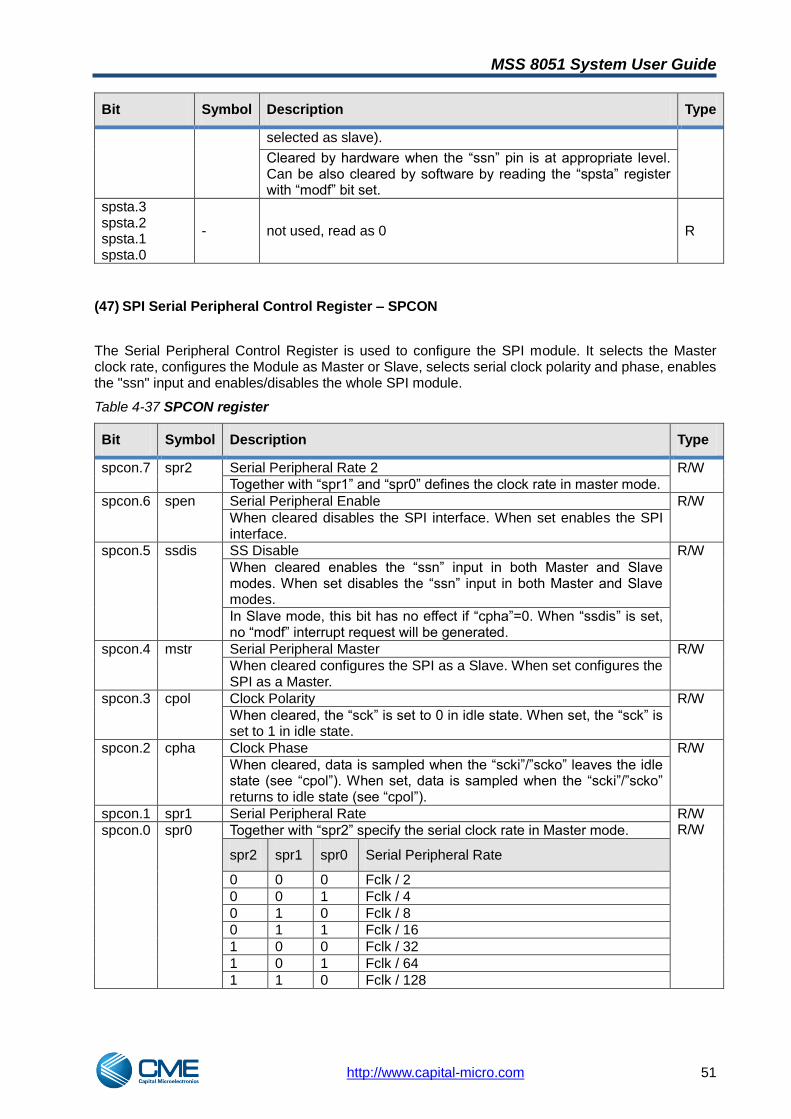
MSS 8051 System User Guide
http://www.capital-micro.com 51
Bit Symbol Description Type
selected as slave).
Cleared by hardware when the ―ssn‖ pin is at appropriate level. Can be also cleared by software by reading the ―spsta‖ register with ―modf‖ bit set.
spsta.3 spsta.2 spsta.1 spsta.0
- not used, read as 0 R
(47) SPI Serial Peripheral Control Register – SPCON
The Serial Peripheral Control Register is used to configure the SPI module. It selects the Master clock rate, configures the Module as Master or Slave, selects serial clock polarity and phase, enables the "ssn" input and enables/disables the whole SPI module.
Table 4-37 SPCON register
Bit Symbol Description Type
spcon.7 spr2 Serial Peripheral Rate 2 R/W
Together with ―spr1‖ and ―spr0‖ defines the clock rate in master mode.
spcon.6 spen Serial Peripheral Enable R/W
When cleared disables the SPI interface. When set enables the SPI interface.
spcon.5 ssdis SS Disable R/W
When cleared enables the ―ssn‖ input in both Master and Slave modes. When set disables the ―ssn‖ input in both Master and Slave modes.
In Slave mode, this bit has no effect if ―cpha‖=0. When ―ssdis‖ is set, no ―modf‖ interrupt request will be generated.
spcon.4 mstr Serial Peripheral Master R/W
When cleared configures the SPI as a Slave. When set configures the SPI as a Master.
spcon.3 cpol Clock Polarity R/W
When cleared, the ―sck‖ is set to 0 in idle state. When set, the ―sck‖ is set to 1 in idle state.
spcon.2 cpha Clock Phase R/W
When cleared, data is sampled when the ―scki‖/‖scko‖ leaves the idle state (see ―cpol‖). When set, data is sampled when the ―scki‖/‖scko‖ returns to idle state (see ―cpol‖).
spcon.1 spr1 Serial Peripheral Rate R/W R/W spcon.0 spr0 Together with ―spr2‖ specify the serial clock rate in Master mode.
spr2 spr1 spr0 Serial Peripheral Rate
0 0 0 Fclk / 2
0 0 1 Fclk / 4
0 1 0 Fclk / 8
0 1 1 Fclk / 16
1 0 0 Fclk / 32
1 0 1 Fclk / 64
1 1 0 Fclk / 128

MSS 8051 System User Guide
http://www.capital-micro.com 52
Bit Symbol Description Type
1 1 1 the master clock is not generated ( when ―cpol‖ = ‗1‘ on the ―scko‖ output is high level, otherwise is low level)
(48) SPI Serial Peripheral Data Register – SPDAT
The SPDAT is a read/write buffer for the ―receive data‖ register. While writing to the SPDAT data is placed directly into the shift register (there is no transmit buffer). Reading the SPDAT returns the value located in the receive buffer, not the shift register.
(49) SPI Serial Peripheral Slave Select Register – SPSSN
The SPSSN is a read/write register used to control the ―spssn [7:0]‖ output bus of the core. Data written to this register is directly available on the ―spssn‖ output. Each of its bits can be used to select a separate external SPI slave device.
(50) Software Reset Register – SRST
The software reset will be accomplished through the SRST SFR register. The contents of this register are presented below.
Table 4-38 SRST register
Bit Symbol Description Type
srst.7 - not used, read as 0 R
srst.6 -
srst.5 -
srst.4 -
srst.3 -
srst.2 -
srst.1 -
srst.0 srstreq Software reset request. R/W
Writing ‗0‘ value to this bit will have no effect. Single writing ‗1‘ value to this bit will have no effect. Double writing ‗1‘ value (in two consecutive instructions) will generate an internal software reset.
Reading this bit will inform about the reset source:
if ‗0‘ – source of last reset sequence was not a software reset (hardware, watchdog or debugger reset); if ‗1‘ – source of last reset sequence was a software reset (caused by double writing ‗1‘ value to the ―srstreq‖ bit).
(51) DMA – Source Address Registers 0, 1, 2
DMAS0: Address – A1h Reset value – 00h
DMAS1: Address – A2h Reset value – 00h
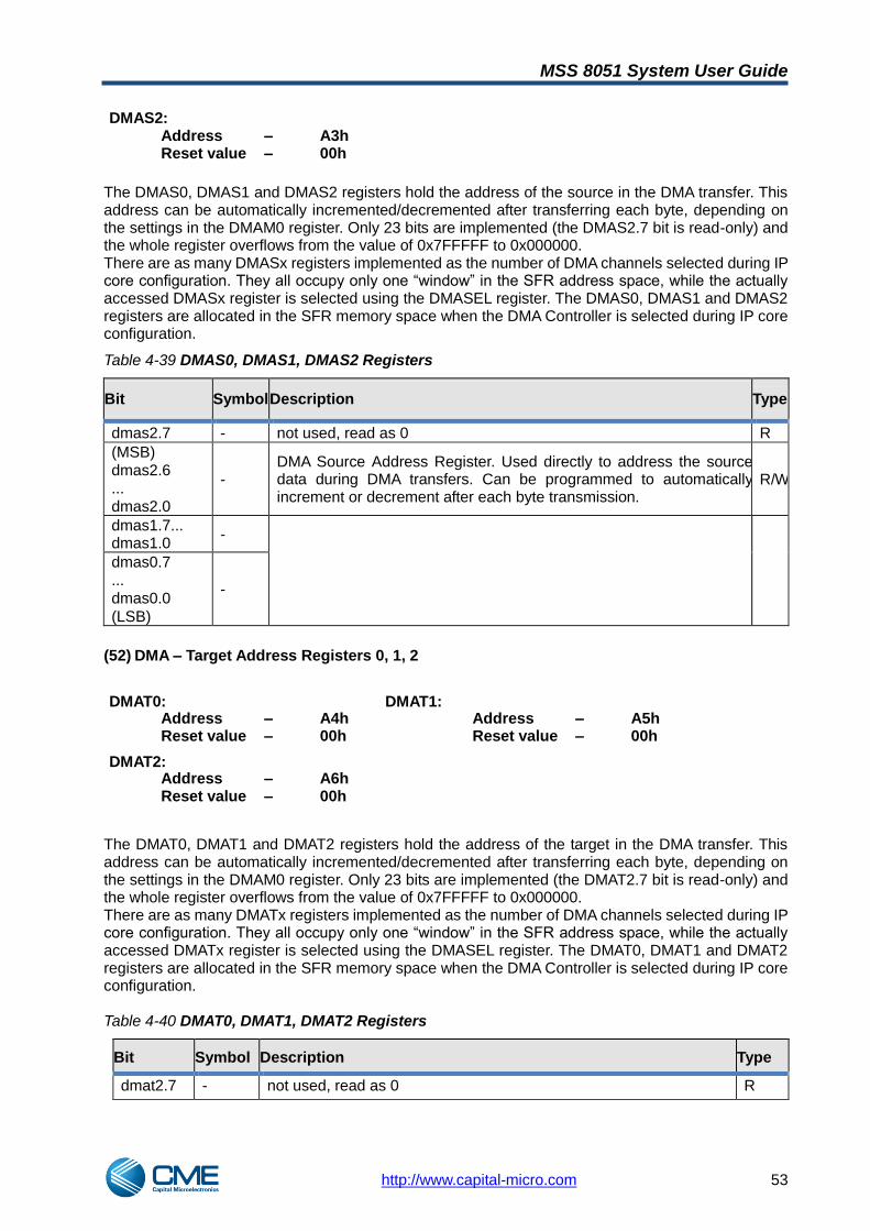
MSS 8051 System User Guide
http://www.capital-micro.com 53
DMAS2: Address – A3h Reset value – 00h
The DMAS0, DMAS1 and DMAS2 registers hold the address of the source in the DMA transfer. This address can be automatically incremented/decremented after transferring each byte, depending on the settings in the DMAM0 register. Only 23 bits are implemented (the DMAS2.7 bit is read-only) and the whole register overflows from the value of 0x7FFFFF to 0x000000. There are as many DMASx registers implemented as the number of DMA channels selected during IP core configuration. They all occupy only one ―window‖ in the SFR address space, while the actually accessed DMASx register is selected using the DMASEL register. The DMAS0, DMAS1 and DMAS2 registers are allocated in the SFR memory space when the DMA Controller is selected during IP core configuration.
Table 4-39 DMAS0, DMAS1, DMAS2 Registers
Bit Symbol Description Type
dmas2.7 - not used, read as 0 R
(MSB) dmas2.6 ... dmas2.0
- DMA Source Address Register. Used directly to address the source data during DMA transfers. Can be programmed to automatically increment or decrement after each byte transmission.
R/W
dmas1.7... dmas1.0
-
dmas0.7 ... dmas0.0
(LSB)
-
(52) DMA – Target Address Registers 0, 1, 2
DMAT0: Address – A4h Reset value – 00h
DMAT1: Address – A5h Reset value – 00h
DMAT2: Address – A6h Reset value – 00h
The DMAT0, DMAT1 and DMAT2 registers hold the address of the target in the DMA transfer. This address can be automatically incremented/decremented after transferring each byte, depending on the settings in the DMAM0 register. Only 23 bits are implemented (the DMAT2.7 bit is read-only) and the whole register overflows from the value of 0x7FFFFF to 0x000000. There are as many DMATx registers implemented as the number of DMA channels selected during IP core configuration. They all occupy only one ―window‖ in the SFR address space, while the actually accessed DMATx register is selected using the DMASEL register. The DMAT0, DMAT1 and DMAT2 registers are allocated in the SFR memory space when the DMA Controller is selected during IP core configuration. Table 4-40 DMAT0, DMAT1, DMAT2 Registers
Bit Symbol Description Type
dmat2.7 - not used, read as 0 R
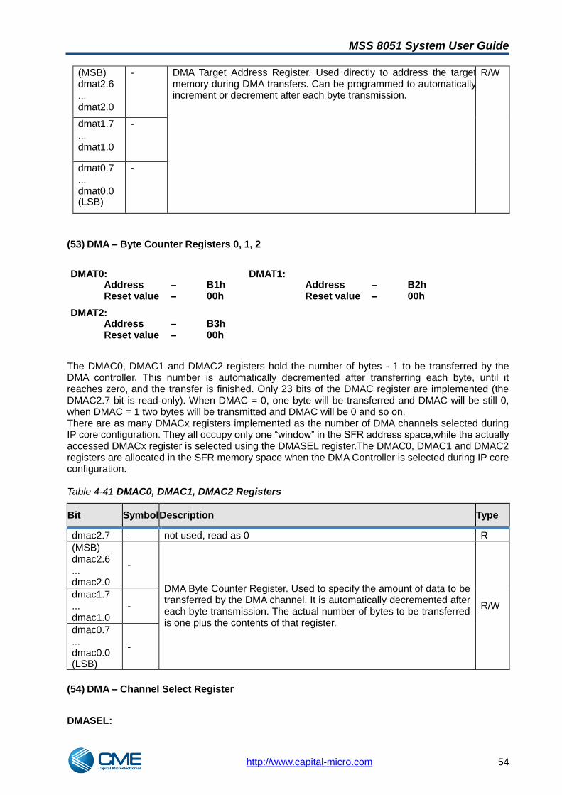
MSS 8051 System User Guide
http://www.capital-micro.com 54
(MSB) dmat2.6 ... dmat2.0
- DMA Target Address Register. Used directly to address the target memory during DMA transfers. Can be programmed to automatically increment or decrement after each byte transmission.
R/W
dmat1.7 ... dmat1.0
-
dmat0.7 ... dmat0.0 (LSB)
-
(53) DMA – Byte Counter Registers 0, 1, 2
DMAT0: Address – B1h Reset value – 00h
DMAT1: Address – B2h Reset value – 00h
DMAT2: Address – B3h Reset value – 00h
The DMAC0, DMAC1 and DMAC2 registers hold the number of bytes - 1 to be transferred by the DMA controller. This number is automatically decremented after transferring each byte, until it reaches zero, and the transfer is finished. Only 23 bits of the DMAC register are implemented (the DMAC2.7 bit is read-only). When DMAC = 0, one byte will be transferred and DMAC will be still 0, when DMAC = 1 two bytes will be transmitted and DMAC will be 0 and so on. There are as many DMACx registers implemented as the number of DMA channels selected during IP core configuration. They all occupy only one ―window‖ in the SFR address space,while the actually accessed DMACx register is selected using the DMASEL register.The DMAC0, DMAC1 and DMAC2 registers are allocated in the SFR memory space when the DMA Controller is selected during IP core configuration.
Table 4-41 DMAC0, DMAC1, DMAC2 Registers
Bit Symbol Description Type
dmac2.7 - not used, read as 0 R
(MSB) dmac2.6 ... dmac2.0
-
DMA Byte Counter Register. Used to specify the amount of data to be transferred by the DMA channel. It is automatically decremented after each byte transmission. The actual number of bytes to be transferred is one plus the contents of that register.
R/W dmac1.7 ... dmac1.0
-
dmac0.7 ... dmac0.0 (LSB)
-
(54) DMA – Channel Select Register
DMASEL:

MSS 8051 System User Guide
http://www.capital-micro.com 55
Address – B1h Reset value – 00h The DMASEL register is used to select the currently accessed set of registers assigned to one of the DMA channels. The other purpose of this register is to manually start the transmission using the actually selected DMA channel. Another feature controlled by the DMASEL register is the type of priority structure between channels (2-level programmable or rotating). The DMASEL register is allocated in the SFR memory space when the DMA Controller is selected during IP core configuration. Table 4-42 DMASEL Register
Bit Symbol Description Type
dmasel.7 dmarun When set to 1, starts the DMA transfer using the currently selected channel (dmasel.0-2). This bit is cleared by hardware after finishing the transfer.
R/W
dmasel.6 - not used, read as 0 R
dmasel.5 -
dmasel.4 dmarot DMA priority mode. When set to 1, the rotating priority is enabled, and after completing the transfer the highest priority is automatically given to the channel with the next following number (ascending). When set to 0, each DMA channel‘s priority can be programmed to one of two levels, and within each level the natural priority is used (channel 0 has the highest priority, channel 1 has lower and so on till the last channel implemented, which has the lowest priority).
R/W
dmasel.3 dmasynch Synchronous Mode flag When set to 1, configures the selected DMA channel to work in the Synchronous Mode, where only a single byte is transferred at a single DMA activity (upon interrupt or software run); when 0, the selected channel works in the Asynchronous Mode, making the transmission of the whole amount of data specified in the DMAC register.
R/W
dmasel.2 - Number of currently selected DMA channel. If the number written to this field exceeds the number of channels implemented, the Channel 0 is accessed.
R/W
dmasel.1 R/W
dmasel.0 R/W
(55) DMA – Mode Register 0
DMAM0: Address – B5h Reset value – 00h The DMAM0 register is used to program the auto-modification of source address and target address independently. After transferring a byte, source/target address can remain the same, or be either incremented or decremented, depending on the settings in the DMAM0 register. The other purpose of the DMAM0 register is to specify the space accessed as source and as target. All the accessible spaces are: Program Memory, External Data Memory, On-Chip Memory (IRAM) and Special Function Registers. The source and target spaces are programmed independently, making it possible to transfer data from and to each of the available spaces. Only the number of bits which equal the size of the selected space‘s address bus are relevant (e.g. when SFR space is selected, only the 7 LSBs of the address are used, the others are ―don‘t care‖). There are as many DMAM0 registers implemented as the number of DMA channels selected during IP core configuration. They all occupy only one ―window‖ in the SFR address space, while the actually accessed DMAM0 register is selected using the DMASEL register. The DMAM0 register is allocated in the SFR memory space when the DMA Controller is selected during IP core configuration.
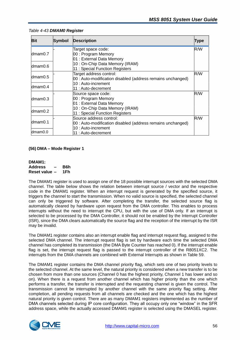
MSS 8051 System User Guide
http://www.capital-micro.com 56
Table 4-43 DMAM0 Register
Bit Symbol Description Type
dmam0.7 - Target space code:
00 : Program Memory 01 : External Data Memory 10 : On-Chip Data Memory (IRAM) 11 : Special Function Registers
R/W
dmam0.6
dmam0.5 - Target address control:
00 : Auto-modification disabled (address remains unchanged) 10 : Auto-increment 11 : Auto-decrement
R/W
dmam0.4
dmam0.3
- Source space code: 00 : Program Memory 01 : External Data Memory 10 : On-Chip Data Memory (IRAM) 11 : Special Function Registers
R/W
dmam0.2
dmam0.1 - Source address control:
00 : Auto-modification disabled (address remains unchanged) 10 : Auto-increment 11 : Auto-decrement
R/W
dmam0.0
(56) DMA – Mode Register 1
DMAM1: Address – B6h Reset value – 1Fh The DMAM1 register is used to assign one of the 18 possible interrupt sources with the selected DMA channel. The table below shows the relation between interrupt source / vector and the respective code in the DMAM1 register. When an interrupt request is generated by the specified source, it triggers the channel to start the transmission. When no valid source is specified, the selected channel can only be triggered by software. After completing the transfer, the selected source flag is automatically cleared by hardware upon request from the DMA controller. This enables to process interrupts without the need to interrupt the CPU, but with the use of DMA only. If an interrupt is selected to be processed by the DMA Controller, it should not be enabled by the Interrupt Controller (ISR), since the DMA clears automatically the source flag and the reception of the interrupt by the ISR may be invalid. The DMAM1 register contains also an interrupt enable flag and interrupt request flag, assigned to the selected DMA channel. The interrupt request flag is set by hardware each time the selected DMA channel has completed its transmission (the DMA Byte Counter has reached 0). If the interrupt enable flag is set, the interrupt request flag is passed to the interrupt controller of the R8051XC2. The interrupts from the DMA channels are combined with External Interrupts as shown in Table 59. The DMAM1 register contains the DMA channel priority flag, which sets one of two priority levels to the selected channel. At the same level, the natural priority is considered when a new transfer is to be chosen from more than one sources (Channel 0 has the highest priority, Channel 1 has lower and so on). When there is a request from another channel which has higher priority than the one which performs a transfer, the transfer is interrupted and the requesting channel is given the control. The transmission cannot be interrupted by another channel with the same priority flag setting. After completion, all pending requests from all channels are checked and the one which has the highest natural priority is given control. There are as many DMAM1 registers implemented as the number of DMA channels selected during IP core configuration. They all occupy only one ―window‖ in the SFR address space, while the actually accessed DMAM1 register is selected using the DMASEL register.

MSS 8051 System User Guide
http://www.capital-micro.com 57
The DMAM1 register is allocated in the SFR memory space when the DMA Controller is selected during IP core configuration. Table 4-44 DMAM1 Register
Bit Symbol Description Type
dmam1.7 dmairq DMA Channel interrupt request flag. Set to 1 by hardware upon transfer completion by current channel. It has to be cleared by software.
R/W
dmam1.6 dmaie DMA Channel interrupt enable. When set to 1, the state of the dmairq flag is passed to the Interrupt Controller. The associated External Interrupt must be enabled to process the DMA interrupt.
R/W
dmam1.5 dmapri DMA Channel priority bit. Programs the selected channel to one of two priority levels (0 – lower, 1 – higher).
R/W
dmam1.4 - DMA Channel trigger selection. Only one of the following sources can be programmed to trigger DMA transfer.
R/W
dmam1.3
dmam1.2 Code Source interrupt
dmam1.1 00000 External Interrupt 0
dmam1.0 00001 Timer 0
00010 External Interrupt 1
00011 Timer 1
00100 Serial Port 0
00101 Timer 2
00110 External Interrupt 7 / I2C
00111 External Interrupt 2 / SPI
01000 External Interrupt 3
01001 External Interrupt 4
01010 External Interrupt 5
01011 External Interrupt 6
01100 Serial Port 1
01101 External Interrupt 8 / DMA Ch 0 & 4
01110 External Interrupt 9 / DMA Ch 1 & 5
01111 External Interrupt 10 / DMA Ch 2 & 6
10000 External Interrupt 11 / DMA Ch 3 & 7
10001 External Interrupt 12
other No interrupt triggers the DMA channel
Table 4-45 DMA Interrupt Vectors
Channel No. Interrupt vector Shared interrupt source
0 0x008B External Interrupt 8
1 0x0093 External Interrupt 9
2 0x009B External Interrupt 10
3 0x00A3 External Interrupt 11
4 0x008B External Interrupt 8
5 0x0093 External Interrupt 9
6 0x009B External Interrupt 10

MSS 8051 System User Guide
http://www.capital-micro.com 58
7 0x00A3 External Interrupt 11
(57) RTC Select Register
Real Time Clock is interfaced through 10 special function registers: six that keep time count (rtcss, rtcs, rtcm, rtch, rtcd1, rtcd0) , three that control the alarm time (rtas, rtam, rtah) and . Its operation is controlled by the rtcc register and ertc (ien4.5) bit. All functions and restrictions on accessing the registers are presented in the ―Special Function Registers‖ section. RTCSEL: Address – E6h Reset value – 00h The purpose of the RTCSEL register is to provide (together with the RTCDAT register) a port to read/write the internal registers of the RTC module.
Table 4-46 RTCSEL Register
Bit Symbol Description Type
rtcsel.7 rtcsel.6 rtcsel.5
- Not used, read as 0 R
rtcsel.4 1:write operation,0: read operation R/W
rtcsel.3 rtcsel.2 rtcsel.1 rtcsel.0
- A 4-bit pointer to internal registers of the RTC R/W
The RTCSEL works as a pointer to another internal SFR of the RTC. After writing the requested register‘s ID to the RTCSEL, it becomes available for reading and writing through the RTCDAT location. The table below lists the internal registers of the RTC module together with their pointer values.
Table 4-47 Internal RTC Register Locations
Register ID(RTCSEL value)
Description
RTCC 0h Real Time Clock Control register
RTCS 1h Real Time Clock Second register
RTCM 2h Real Time Clock Minute register
RTCH 3h Real Time Clock Hour register
RTCW 4h Real Time Week register
RTCD0 5h Real Time Clock Day register 0
RTCD1 6h Real Time Clock Day register 1
RTAS 8h Real Time Alarm Second register
RTAM 9h Real Time Alarm Minute register
RTAH Ah Real Time Alarm Hour register
(58) RTC Data Register
RTCDATA:

MSS 8051 System User Guide
http://www.capital-micro.com 59
Address – E7h Reset value – 00h
The purpose of the RTCDAT register is to provide (together with the RTCSEL register) a port to read/write the internal registers of the RTC module.
(59) RTC Command Register
RTCCMD: Address – E5h Reset value – 00h
Table 4-48 RTCCMD Register
Bit Symbol Description Type
rtccmd.7 - WRITE go 1: write serial command, self cleared when done
R/W
rtccmd.6 rtccmd.5 rtccmd.4 rtccmd.3 rtccmd.2 rtccmd.1 rtccmd.0 rtcsel.0
- Not used, read as 0 R
The purpose of the RTCCMD register is to make trigger the read/write operation from/to the internal registers of the RTC module.
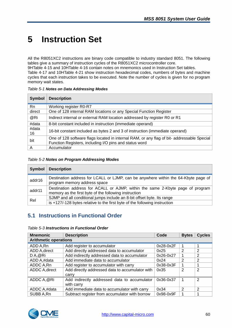
MSS 8051 System User Guide
http://www.capital-micro.com 60
5 Instruction Set
All the R8051XC2 instructions are binary code compatible to industry standard 8051. The following tables give a summary of instruction cycles of the R8051XC2 microcontroller core. 9HTable 4-15 and 10HTable 4-16 contain notes on mnemonics used in Instruction Set tables. Table 4-17 and 10HTable 4-21 show instruction hexadecimal codes, numbers of bytes and machine cycles that each instruction takes to be executed. Note the number of cycles is given for no program memory wait states.
Table 5-1 Notes on Data Addressing Modes
Symbol Description
Rn Working register R0-R7 direct One of 128 internal RAM locations or any Special Function Register
@Ri Indirect internal or external RAM location addressed by register R0 or R1
#data 8-bit constant included in instruction (immediate operand) #data 16
16-bit constant included as bytes 2 and 3 of instruction (immediate operand)
bit One of 128 software flags located in internal RAM, or any flag of bit- addressable Special Function Registers, including I/O pins and status word
A Accumulator
Table 5-2 Notes on Program Addressing Modes
Symbol Description
addr16 Destination address for LCALL or LJMP, can be anywhere within the 64-Kbyte page of program memory address space
addr11 Destination address for ACALL or AJMP, within the same 2-Kbyte page of program memory as the first byte of the following instruction
Rel SJMP and all conditional jumps include an 8-bit offset byte. Its range
is +127/-128 bytes relative to the first byte of the following instruction
5.1 Instructions in Functional Order
Table 5-3 Instructions in Functional Order
Mnemonic Description Code Bytes Cycles Arithmetic operations
ADD A,Rn Add register to accumulator 0x28-0x2F 1 1 ADD A,direct Add directly addressed data to accumulator 0x25 2 2 D A,@Ri Add indirectly addressed data to accumulator 0x26-0x27 1 2 ADD A,#data Add immediate data to accumulator 0x24 2 2 ADDC A,Rn Add register to accumulator with carry 0x38-0x3F 1 1 ADDC A,direct Add directly addressed data to accumulator with
carry 0x35 2 2
ADDC A,@Ri Add indirectly addressed data to accumulator with carry
0x36-0x37 1 2
ADDC A,#data Add immediate data to accumulator with carry 0x34 2 2 SUBB A,Rn Subtract register from accumulator with borrow 0x98-0x9F 1 1
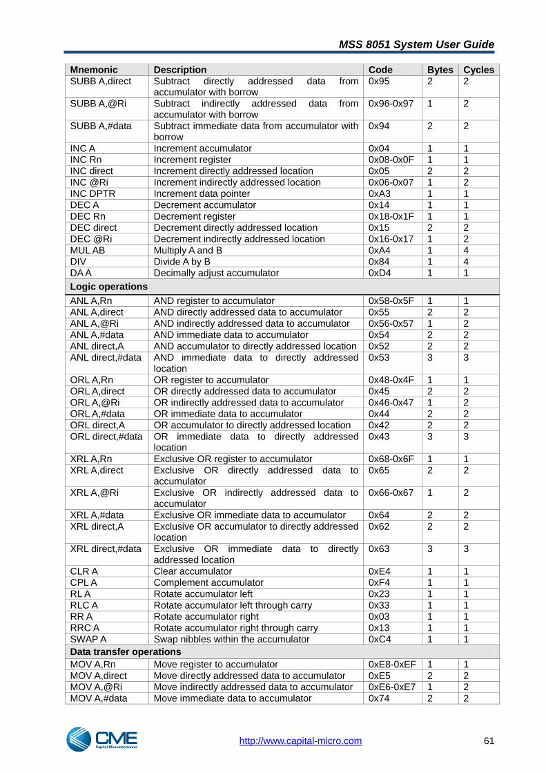
MSS 8051 System User Guide
http://www.capital-micro.com 61
Mnemonic Description Code Bytes Cycles SUBB A,direct Subtract directly addressed data from
accumulator with borrow 0x95 2 2
SUBB A,@Ri Subtract indirectly addressed data from accumulator with borrow
0x96-0x97 1 2
SUBB A,#data Subtract immediate data from accumulator with borrow
0x94 2 2
INC A Increment accumulator 0x04 1 1 INC Rn Increment register 0x08-0x0F 1 1 INC direct Increment directly addressed location 0x05 2 2 INC @Ri Increment indirectly addressed location 0x06-0x07 1 2 INC DPTR Increment data pointer 0xA3 1 1 DEC A Decrement accumulator 0x14 1 1 DEC Rn Decrement register 0x18-0x1F 1 1 DEC direct Decrement directly addressed location 0x15 2 2 DEC @Ri Decrement indirectly addressed location 0x16-0x17 1 2 MUL AB Multiply A and B 0xA4 1 4 DIV Divide A by B 0x84 1 4 DA A Decimally adjust accumulator 0xD4 1 1
Logic operations
ANL A,Rn AND register to accumulator 0x58-0x5F 1 1 ANL A,direct AND directly addressed data to accumulator 0x55 2 2 ANL A,@Ri AND indirectly addressed data to accumulator 0x56-0x57 1 2 ANL A,#data AND immediate data to accumulator 0x54 2 2 ANL direct,A AND accumulator to directly addressed location 0x52 2 2 ANL direct,#data AND immediate data to directly addressed
location 0x53 3 3
ORL A,Rn OR register to accumulator 0x48-0x4F 1 1 ORL A,direct OR directly addressed data to accumulator 0x45 2 2 ORL A,@Ri OR indirectly addressed data to accumulator 0x46-0x47 1 2 ORL A,#data OR immediate data to accumulator 0x44 2 2 ORL direct,A OR accumulator to directly addressed location 0x42 2 2 ORL direct,#data OR immediate data to directly addressed
location 0x43 3 3
XRL A,Rn Exclusive OR register to accumulator 0x68-0x6F 1 1 XRL A,direct Exclusive OR directly addressed data to
accumulator 0x65 2 2
XRL A,@Ri Exclusive OR indirectly addressed data to accumulator
0x66-0x67 1 2
XRL A,#data Exclusive OR immediate data to accumulator 0x64 2 2 XRL direct,A Exclusive OR accumulator to directly addressed
location 0x62 2 2
XRL direct,#data Exclusive OR immediate data to directly addressed location
0x63 3 3
CLR A Clear accumulator 0xE4 1 1 CPL A Complement accumulator 0xF4 1 1 RL A Rotate accumulator left 0x23 1 1 RLC A Rotate accumulator left through carry 0x33 1 1 RR A Rotate accumulator right 0x03 1 1 RRC A Rotate accumulator right through carry 0x13 1 1 SWAP A Swap nibbles within the accumulator 0xC4 1 1
Data transfer operations
MOV A,Rn Move register to accumulator 0xE8-0xEF 1 1 MOV A,direct Move directly addressed data to accumulator 0xE5 2 2 MOV A,@Ri Move indirectly addressed data to accumulator 0xE6-0xE7 1 2 MOV A,#data Move immediate data to accumulator 0x74 2 2
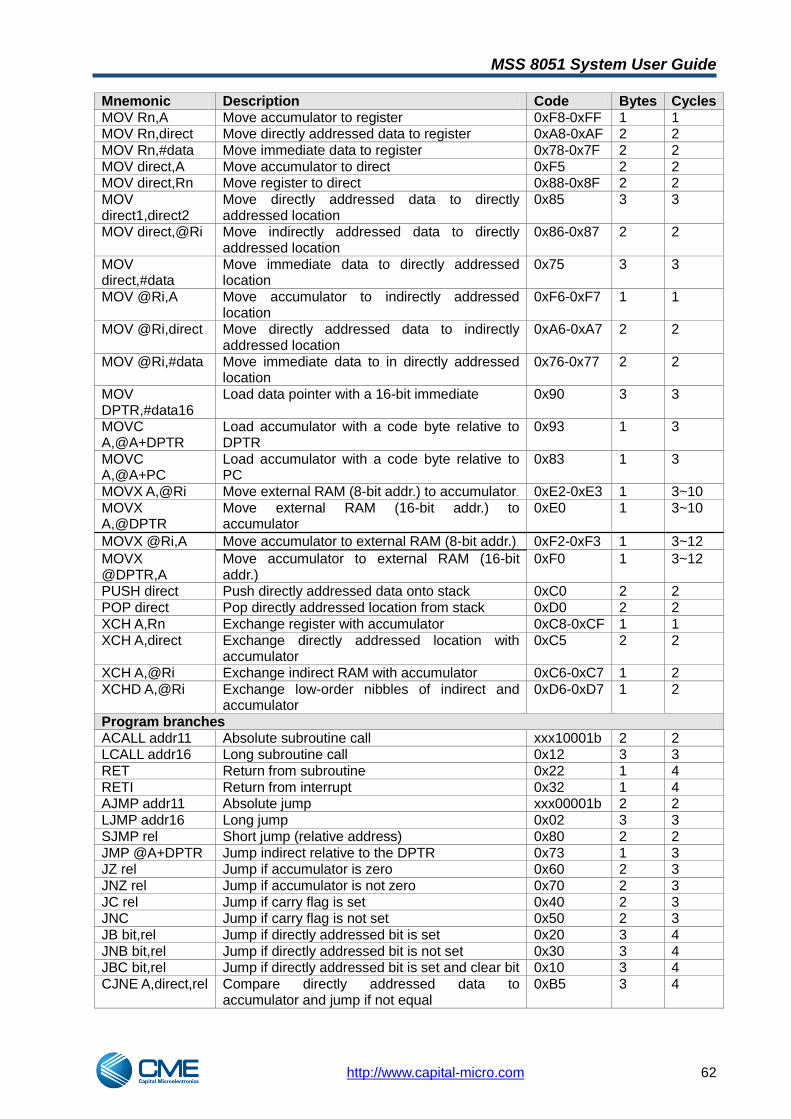
MSS 8051 System User Guide
http://www.capital-micro.com 62
Mnemonic Description Code Bytes Cycles MOV Rn,A Move accumulator to register 0xF8-0xFF 1 1 MOV Rn,direct Move directly addressed data to register 0xA8-0xAF 2 2 MOV Rn,#data Move immediate data to register 0x78-0x7F 2 2 MOV direct,A Move accumulator to direct 0xF5 2 2 MOV direct,Rn Move register to direct 0x88-0x8F 2 2 MOV direct1,direct2
Move directly addressed data to directly addressed location
0x85 3 3
MOV direct,@Ri Move indirectly addressed data to directly addressed location
0x86-0x87 2 2
MOV direct,#data
Move immediate data to directly addressed location
0x75 3 3
MOV @Ri,A Move accumulator to indirectly addressed location
0xF6-0xF7 1 1
MOV @Ri,direct Move directly addressed data to indirectly addressed location
0xA6-0xA7 2 2
MOV @Ri,#data Move immediate data to in directly addressed location
0x76-0x77 2 2
MOV DPTR,#data16
Load data pointer with a 16-bit immediate 0x90 3 3
MOVC A,@A+DPTR
Load accumulator with a code byte relative to DPTR
0x93 1 3
MOVC A,@A+PC
Load accumulator with a code byte relative to PC
0x83 1 3
MOVX A,@Ri Move external RAM (8-bit addr.) to accumulator0F0F 0xE2-0xE3 1 3~10 MOVX A,@DPTR
Move external RAM (16-bit addr.) to accumulator
0xE0 1 3~10
MOVX @Ri,A Move accumulator to external RAM (8-bit addr.)12H 0xF2-0xF3 1 3~12
MOVX @DPTR,A
Move accumulator to external RAM (16-bit addr.)13H
0xF0 1 3~12
PUSH direct Push directly addressed data onto stack 0xC0 2 2 POP direct Pop directly addressed location from stack 0xD0 2 2 XCH A,Rn Exchange register with accumulator 0xC8-0xCF 1 1 XCH A,direct Exchange directly addressed location with
accumulator 0xC5 2 2
XCH A,@Ri Exchange indirect RAM with accumulator 0xC6-0xC7 1 2 XCHD A,@Ri Exchange low-order nibbles of indirect and
accumulator 0xD6-0xD7 1 2
Program branches ACALL addr11 Absolute subroutine call xxx10001b 2 2 LCALL addr16 Long subroutine call 0x12 3 3 RET Return from subroutine 0x22 1 4 RETI Return from interrupt 0x32 1 4 AJMP addr11 Absolute jump xxx00001b 2 2 LJMP addr16 Long jump 0x02 3 3 SJMP rel Short jump (relative address) 0x80 2 2 JMP @A+DPTR Jump indirect relative to the DPTR 0x73 1 3 JZ rel Jump if accumulator is zero 0x60 2 3 JNZ rel Jump if accumulator is not zero 0x70 2 3 JC rel Jump if carry flag is set 0x40 2 3 JNC Jump if carry flag is not set 0x50 2 3 JB bit,rel Jump if directly addressed bit is set 0x20 3 4 JNB bit,rel Jump if directly addressed bit is not set 0x30 3 4 JBC bit,rel Jump if directly addressed bit is set and clear bit 0x10 3 4 CJNE A,direct,rel Compare directly addressed data to
accumulator and jump if not equal 0xB5 3 4

MSS 8051 System User Guide
http://www.capital-micro.com 63
Mnemonic Description Code Bytes Cycles CJNE A,#data,rel
Compare immediate data to accumulator and jump if not equal
0xB4 3 4
CJNE Rn,#data,rel
Compare immediate data to register and jump if not equal
0xB8-0xBF 3 4
CJNE @Ri,#data,rel
Compare immed. to ind. and jump if not equal B6-B7 3 5
DJNZ Rn,rel Decrement register and jump if not zero D8-DF 2 3 DJNZ direct,rel Decrement directly addressed location and
jump if not zero D5 3 4
NOP No operation 0 1 1 Boolean manipulation CLR C Clear carry flag 0xC3 1 1 CLR bit Clear directly addressed bit 0xC2 2 2 SETB C Set carry flag 0xD3 1 1 SETB bit Set directly addressed bit 0xD2 2 2 CPL C Complement carry flag 0xB3 1 2 CPL bit Complement directly addressed bit 0xB2 2 2 ANL C,bit AND directly addressed bit to carry flag 0x82 2 2 ANL C,/bit AND complement of directly addressed bit to
carry 0xB0 2 2
ORL C,bit OR directly addressed bit to carry flag 0x72 2 2 ORL C,/bit OR complement of directly addressed bit to
carry 0xA0 2 2
MOV C,bit Move directly addressed bit to carry flag 0xA2 2 2 MOV bit,C Move carry flag to directly addressed bit 0x92 2 2
5.2 Instructions in hexadecimal order
Table 5-4 Instructions in hexadecimal order
Opcode Mnemonic
00 H NOP
01 H AJMP addr11
02 H LJMP addr16
03 H RR A
04 H INC A
05 H INC direct
06 H INC @R0
07 H INC @R1
08 H INC R0
09 H INC R1
0A H INC R2
0B H INC R3
0C H INC R4
0D H INC R5
0E H INC R6
0F H INC R7
10 H JBC bit,rel
11 H ACALL addr11
12 H LCALL addr16
13 H RRC A
14 H DEC A
15 H DEC direct
Opcode Mnemonic
16 H DEC @R0
17 H DEC @R1
18 H DEC R0
19 H DEC R1
1A H DEC R2
1B H DEC R3
1C H DEC R4
1D H DEC R5
1E H DEC R6
1F H DEC R7
20 H JB bit.rel
21 H AJMP addr11
22 H RET
23 H RL A
24 H ADD A,#data
25 H ADD A,direct
26 H ADD A,@R0
27 H ADD A,@R1
28 H ADD A,R0
29 H ADD A,R1
2A H ADD A,R2
2B H ADD A,R3
Opcode Mnemonic
2C H ADD A,R4
2D H ADD A,R5
2E H ADD A,R6
2F H ADD A,R7
30 H JNB bit,rel
31 H ACALL addr11
32 H RETI
33 H RLC A
34 H ADDC A,#data
35 H ADDC A,direct
36 H ADDC A,@R0
37 H ADDC A,@R1
38 H ADDC A,R0
39 H ADDC A,R1
3A H ADDC A,R2
3B H ADDC A,R3
3C H ADDC A,R4
3D H ADDC A,R5
3E H ADDC A,R6
3F H ADDC A,R7
40 H JC rel
41 H AJMP addr11
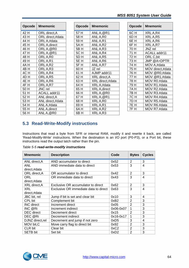
MSS 8051 System User Guide
http://www.capital-micro.com 64
Opcode Mnemonic
42 H ORL direct,A
43 H ORL direct,#data
44 H ORL A,#data
45 H ORL A,direct
46 H ORL A,@R0
47 H ORL A,@R1
48 H ORL A,R0
49 H ORL A,R1
4A H ORL A,R2
4B H ORL A,R3
4C H ORL A,R4
4D H ORL A,R5
4E H ORL A,R6
4F H ORL A,R7
50 H JNC rel
51 H ACALL addr11
52 H ANL direct,A
53 H ANL direct,#data
54 H ANL A,#data
55 H ANL A,direct
56 H ANL A,@R0
Opcode Mnemonic
57 H ANL A,@R1
58 H ANL A,R0
59 H ANL A,R1
5A H ANL A,R2
5B H ANL A,R3
5C H ANL A,R4
5D H ANL A,R5
5E H ANL A,R6
5F H ANL A,R7
60 H JZ rel
61 H AJMP addr11
62 H XRL direct,A
63 H XRL direct,#data
64 H XRL A,#data
65 H XRL A,direct
66 H XRL A,@R0
67 H XRL A,@R1
68 H XRL A,R0
69 H XRL A,R1
6A H XRL A,R2
6B H XRL A,R3
Opcode Mnemonic
6C H XRL A,R4
6D H XRL A,R5
6E H XRL A,R6
6F H XRL A,R7
70 H JNZ rel
71 H ACALL addr11
72 H ORL C,bit
73 H JMP @A+DPTR
74 H MOV A,#data
75 H MOV direct,#data
76 H MOV @R0,#data
77 H MOV @R1,#data
78 H MOV R0.#data
79 H MOV R1.#data
7A H MOV R2.#data
7B H MOV R3.#data
7C H MOV R4.#data
7D H MOV R5.#data
7E H MOV R6.#data
7F H MOV R7.#data
5.3 Read-Write-Modify instructions
Instructions that read a byte from SFR or internal RAM, modify it and rewrite it back, are called 'Read-Modify-Write' instructions. When the destination is an I/O port (P0-P3), or a Port bit, these instructions read the output latch rather than the pin.
Table 5-5 read-write-modify instructions
Mnemonic Description Code Bytes Cycles
ANL direct,A AND accumulator to direct 0x52 2 3
ANL direct,#data
AND immediate data to direct 0x53 3 4
ORL direct,A OR accumulator to direct 0x42 2 3
ORL direct,#data
OR immediate data to direct 0x43 3 4
XRL direct,A Exclusive OR accumulator to direct 0x62 2 3 XRL direct,#data
Exclusive OR immediate data to direct 0x63 3 4
JBC bit, rel Jump if bit is set and clear bit 0x10 3 4 CPL bit Complement bit 0xB2 2 3 INC direct Increment direct 0x05 2 3 INC @Ri Increment indirect 0x06-0x07 1 3 DEC direct Decrement direct 0x15 2 3 DEC @Ri Decrement indirect 0x16-0x17 1 3 DJNZ direct,rel Decrement and jump if not zero 0xD5 3 4
MOV bit,C Move carry flag to direct bit 0x92 2 3 CLR bit Clear bit 0xC2 2 3 SETB bit Set bit 0xD2 2 3
MSS 8051 System User Guide
http://www.capital-micro.com 65
5.4 Instruction duration calculation
To accurately estimate program execution time, the execution duration of each instruction is needed to be calculated. The duration of each instruction can be calculated using the formula below: if (BYTES > 1 or CYCLES = 1) then DURATION = CYCLES + (BYTES+R)*P + X*D else DURATION = CYCLES + (2+R)*P + X*D Wherein:
- BYTES is the number of bytes for the instruction (see Table above 14H) - CYCLES is the number of cycles for no wait states (see 16H Table above) - R = 1 for the MOVC instruction, otherwise R = 0
- X = 1 for MOVX instructions, otherwise X = 0
- P = number of program memory wait states (= ‗ckcon [6:4]‘) - D = number of data memory wait states (= ‗ckcon [2:0]‘).
In the Program Memory Write mode (PMW) the formula for MOVX is as follows: DURATION = CYCLES + (2+X)*P Table above
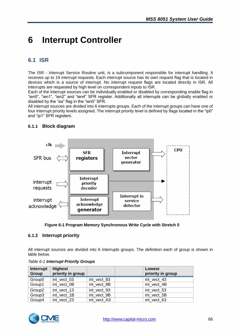
MSS 8051 System User Guide
http://www.capital-micro.com 66
6 Interrupt Controller
6.1 ISR
The ISR - Interrupt Service Routine unit, is a subcomponent responsible for interrupt handling. It receives up to 19 interrupt requests. Each interrupt source has its own request flag that is located in devices which is a source of interrupt. No interrupt request flags are located directly in ISR. All interrupts are requested by high level on correspondent inputs to ISR. Each of the interrupt sources can be individually enabled or disabled by corresponding enable flag in ―ien0‖, ―ien1‖, ―ien2‖ and ―ien4‖ SFR register. Additionally all interrupts can be globally enabled or disabled by the ―ea‖ flag in the ―ien0‖ SFR. All interrupt sources are divided into 6 interrupts groups. Each of the interrupt groups can have one of four interrupt priority levels assigned. The interrupt priority level is defined by flags located in the ―ip0‖ and ―ip1‖ SFR registers.
6.1.1 Block diagram
Figure 6-1 Program Memory Synchronous Write Cycle with Stretch 0
6.1.2 Interrupt priority
All interrupt sources are divided into 6 interrupts groups. The definition each of group is shown in table below.
Table 6-1 Interrupt Priority Groups
Interrupt Group
Highest priority in group
Lowest priority in group
Group0 int_vect_03 int_vect_83 int_vect_43 Group1 int_vect_0B int_vect_8B int_vect_4B
Group2 int_vect_13 int_vect_93 int_vect_53
Group3 int_vect_1B int_vect_9B int_vect_5B Group4 int_vect_23 int_vect_A3 int_vect_63

MSS 8051 System User Guide
http://www.capital-micro.com 67
Interrupt Group
Highest priority in group
Lowest priority in group
Group5 int_vect_2B int_vect_AB int_vect_EB int_vect_6B Inside group there is, fixed by hardware, interrupt priority structure. Sources from first column have the highest priority (inside group), sources from second column have middle priority and interrupts sources from third column have the lowest priority. There is no possibility to change interrupt priority inside the group. There is also an interrupt priority structure between the groups. Group0 has the highest priority and Group5 has the lowest. The priority between groups can be programmed by changing priority level (priority level can be set from 0 to 3) assigned to each group. The priority level of interrupt group is defined by flags of the ―ip0‖ and ―ip1‖ SFR registers. Relations between flags in ―ip0‖ and ―ip1‖ SFR registers and interrupt groups are defined in the table below. Table 6-2 Interrupt Priority between Groups
Interrupt Group
Priority within this same priority level
IP1 bit IP0 bit
Group0 Highest 0 0 Group1 1 1
Group2 2 2
Group3 3 3
Group4 4 4
Group5 Lowest 5 5
The settings of interrupt priority flags and priority level are shown in table below. Table 6-3 Interrupt Priority Levels
Level Priority IP1.x bit IP0.x bit
Level0 Lowest 0 0
Level1 0 1
Level2 1 0
Level3 Highest 1 1
All priority types are taken into account when more than one interrupt is requested. The most important is the priority level set by IP0 and IP1 registers, then the natural priority between groups, and at last the priority inside each group. To determine which interrupt has the highest priority (which must be serviced in the first order) the following steps are made. From all groups there are chosen those which have the highest priority level. From those with the highest priority level there is chosen one with the highest natural priority
between groups. From group with highest priority there is chosen the interrupt with the highest priority inside the
group. What is important is that currently running interrupt service subroutine can be interrupted only by interrupt with higher priority level. No interrupt with the same or lower priority level can interrupt the currently running interrupt service subroutine. Therefore there can be maximum four interrupts in service at the same time. ATTENTION: When some interrupt is requested with priority X, the invoked subroutine has priority level X even though priority level for sources has been changed; this interrupt subroutine can be

MSS 8051 System User Guide
http://www.capital-micro.com 68
interrupted only by interrupt with priority higher than X. Table 6-4 Summary of interrupt sources
Source Vector Address Vector Number
Interrupt Group
External Interrupt 0 0003H 0 0
Timer0 overflow 000BH 1 1
External Interrupt 1 0013H 2 2
Timer1 overflow 001BH 3 3
Serial Port 0 interrupt 0023H 4 4
Timer2 interrupt 002BH 5 5
External Interrupt 7/I2C interrupt 0043H 8 0
External Interrupt 2/SPI interrupt 004BH 9 1
External Interrupt 3 0053H 10 2
External Interrupt 4 005BH 11 3
External Interrupt 5 0063H 12 4
External Interrupt 6 006BH 13 5
Serial Port 1 interrupt 0083H 16 0
External Interrupt 8 / DMA Channel 0 & 4 008BH 17 1
External Interrupt 9 / DMA Channel 1 & 5 0093H 18 2
External Interrupt 10 / DMA Channel 2 & 6 009BH 19 3
External Interrupt 11 / DMA Channel 3 & 7 00A3H 20 4
External Interrupt 12 00ABH 21 5
RTC Interrupt 00EBH 29 5
6.2 EXINT
6.2.1 External Interrupt 0 and 1
The External interrupts 0 and 1 can be programmed to be either low level triggered or falling transaction triggered, depending on bit IT0 and IT1. The bits IE0 and IE1 in the TCON register are the flags which are checked to generate the interrupt. In the edge triggered mode, the INTx inputs are sampled in every machine cycle. If the sample is high in one cycle and low in the next, then a falling transition is detected and the interrupts request flag IEx is set. The rising transition is detected as the same way. The flag bit requests the interrupt. Since the external interrupts are sampled every machine cycle, the have to be held high or low for at least one complete machine cycle. The IEx flag is automatically cleared when the service routine is called. If the level triggered mode is selected, then the requesting source has to hold the pin low till the interrupt is serviced. The IEx flag will not be cleared by the hardware on entering the service routine. If the interrupt continues to be held low even after the service routine is completed, then the
MSS 8051 System User Guide
http://www.capital-micro.com 69
processor may acknowledge another interrupt request from the same source. The interrupt can also be triggered by setting the corresponding flag bit by software.
6.2.2 External Interrupt 2
The External Interrupt 2 can be programmed to be positive or negative edge sensitive (depending on ―i2fr‖ bit in ―t2con‖. When the chosen edge occurs, bit ―iex2‖ in ―ircon‖ SFR register is set and corresponding interrupt is invoked. Interrupt request flag ―iex2‖ in ―ircon‖ is cleared by hardware automatically when the service routine is vectored to.
6.2.3 External Interrupt 3
The External interrupts 3 can be programmed to be either rising or falling transaction triggered, depending on bit I3FR in the T2CON register. The bit IEX3 in the IRCON register is the flag which is checked to generate the interrupt. Additionally the flag bit can be set (and interrupt invoked) by the Compare/Capture Unit (0). The Compare/Capture Unit sets the flag bit when compare/capture mode is set to compare mode (flags cocal0=0 and cocah0=1 in CCEN register) and the value in Timer 2 becomes equal to the value of compare register CRC. The external interrupt configuration (falling or rising edge sensitive) also applies here. The I3FR defines the edge which generates interrupt, which means that it is also possible to generate interrupt when the contents of Timer 2 become not equal to the CRC register. The flag bit is set by Compare/Capture Unit only when cocal0=0 and cocah0=1. In all others cases the flag bit is set when corresponding edge on external pin occurs. It is impossible to use both External Interrupt and interrupt from CCU at this same time. The flag bit is automatically cleared when the service routine is called.
6.2.4 External Interrupt 4
The External interrupts 4 is only rising transaction triggered. The bit IEX4 in the IRCON register is the flag which is checked to generate the interrupt. Additionally the flag bit can be set (and interrupt invoked) by the Compare/Capture Unit. The Compare/Capture Unit sets the flag bit when compare/capture mode is set to compare mode (flags cocal1=0 and cocah1=1 in CCEN register) and the value in Timer 2 becomes equal to the value of compare register CC1. The flag bit is automatically cleared when the service routine is called.
6.2.5 External Interrupt 5
The External interrupts 5 is only rising transaction triggered. The bit IEX5 in the IRCON register is the flag which is checked to generate the interrupt. Additionally the flag bit can be set (and interrupt invoked) by the Compare/Capture Unit. The Compare/Capture Unit sets the flag bit when compare/capture mode is set to compare mode (flags cocal2=0 and cocah2=1 in CCEN register) and the value in Timer 2 becomes equal to the value of compare register CC2. The flag bit is automatically cleared when the service routine is called.
MSS 8051 System User Guide
http://www.capital-micro.com 70
6.2.6 External Interrupt 6
The External interrupts 6 is only rising transaction triggered. The bit IEX6 in the IRCON register is the flag which is checked to generate the interrupt. Additionally the flag bit can be set (and interrupt invoked) by the Compare/Capture Unit. The Compare/Capture Unit sets the flag bit when compare/capture mode is set to compare mode (flags cocal3=0 and cocah3=1 in CCEN register) and the value in Timer 2 becomes equal to the value of compare register CC3. The ―iex6‖ flag is cleared by hardware automatically when invoked service routine is vectored to.
6.2.7 External Interrupt 7
The External Interrupt 7 is only rising edge sensitive. When a rising edge occurs, the ―iex7‖ flag in ―ircon‖ SFR register is set and corresponding interrupt is invoked. Low or high level at ―int7‖ input pin must be at least 1 clock cycle long for the rising edge to be detected. The ―iex7‖ flag is cleared by hardware automatically when invoked service routine is vectored to.
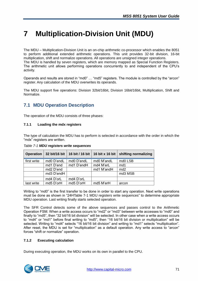
MSS 8051 System User Guide
http://www.capital-micro.com 71
7 Multiplication-Division Unit (MDU)
The MDU – Multiplication-Division Unit is an on-chip arithmetic co-processor which enables the 8051 to perform additional extended arithmetic operations. This unit provides 32-bit division, 16-bit multiplication, shift and normalize operations. All operations are unsigned integer operations. The MDU is handled by seven registers, which are memory mapped as Special Function Registers. The arithmetic unit allows performing operations concurrently to and independent of the CPU‘s activity. Operands and results are stored in ―md0‖ … ―md5‖ registers. The module is controlled by the ―arcon‖ register. Any calculation of the MDU overwrites its operands. The MDU support five operations: Division 32bit/16bit, Division 16bit/16bit, Multiplication, Shift and Normalize.
7.1 MDU Operation Description
The operation of the MDU consists of three phases:
7.1.1 Loading the mdx registers
The type of calculation the MDU has to perform is selected in accordance with the order in which the ―mdx‖ registers are written.
Table 7-1 MDU registers write sequences
Operation 32 bit/16 bit 16 bit / 16 bit 16 bit x 16 bit shifting normalizing
first write md0 D‘endL md0 D‘endL md0 M‘andL md0 LSB
md1 D‘end md1 D‘endH md4 M‘erL md1
md2 D‘end md1 M‘andH md2
md3 D‘endH md3 MSB
md4 D‘orL md4 D‘orL
last write md5 D‘orH md5 D‘orH md5 M‘erH arcon
Writing to ―md0‖ is the first transfer to be done in order to start any operation. Next write operations must be done as shown in ―24HTable 7-1 MDU registers write sequences‖ to determine appropriate MDU operation. Last writing finally starts selected operation. The SFR Control detects some of the above sequences and passes control to the Arithmetic Operation FSM. When a write access occurs to ―md2‖ or ―md3‖ between write accesses to ―md0‖ and finally to ―md5‖, then ―32 bit/16 bit division‖ will be selected. In other case when a write access occurs to ―md4‖ or ―md1‖ before final writing to ―md5‖, then ―16 bit/16 bit division or multiplication‖ will be selected. Writing to ―md4‖ selects ―16 bit/16 bit division‖ and writing to ―md1‖ selects ―multiplication‖. After reset, the MDU is set for ―multiplication‖ as a default operation. Any write access to ―arcon‖ forces ―shift or normalize‖ operation.
7.1.2 Executing calculation
During executing operation, the MDU works on its own in parallel to the CPU.
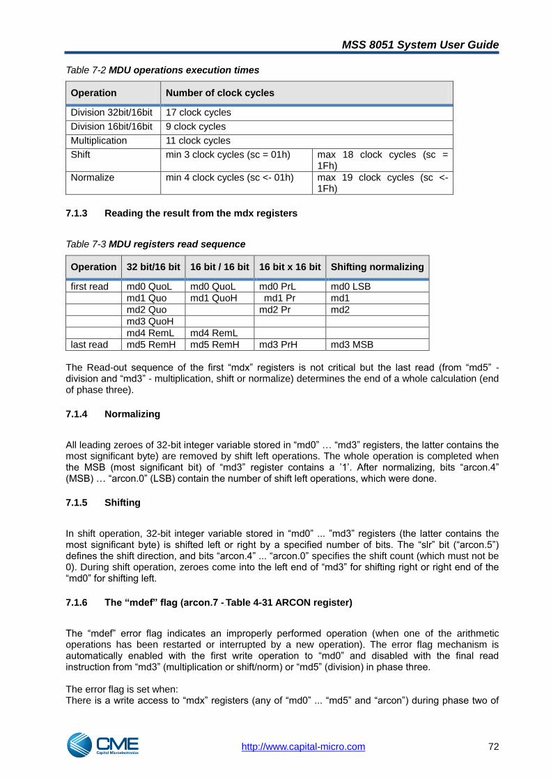
MSS 8051 System User Guide
http://www.capital-micro.com 72
Table 7-2 MDU operations execution times
Operation Number of clock cycles
Division 32bit/16bit 17 clock cycles
Division 16bit/16bit 9 clock cycles
Multiplication 11 clock cycles
Shift min 3 clock cycles (sc = 01h) max 18 clock cycles (sc = 1Fh)
Normalize min 4 clock cycles (sc <- 01h) max 19 clock cycles (sc <- 1Fh)
7.1.3 Reading the result from the mdx registers
Table 7-3 MDU registers read sequence
Operation 32 bit/16 bit 16 bit / 16 bit 16 bit x 16 bit Shifting normalizing
first read md0 QuoL md0 QuoL md0 PrL md0 LSB
md1 Quo md1 QuoH md1 Pr md1
md2 Quo md2 Pr md2
md3 QuoH
md4 RemL md4 RemL
last read md5 RemH md5 RemH md3 PrH md3 MSB
The Read-out sequence of the first ―mdx‖ registers is not critical but the last read (from ―md5‖ - division and ―md3‖ - multiplication, shift or normalize) determines the end of a whole calculation (end of phase three).
7.1.4 Normalizing
All leading zeroes of 32-bit integer variable stored in ―md0‖ … ―md3‖ registers, the latter contains the most significant byte) are removed by shift left operations. The whole operation is completed when the MSB (most significant bit) of ―md3‖ register contains a ‘1‘. After normalizing, bits ―arcon.4‖ (MSB) … ―arcon.0‖ (LSB) contain the number of shift left operations, which were done.
7.1.5 Shifting
In shift operation, 32-bit integer variable stored in ―md0‖ ... ‖md3‖ registers (the latter contains the most significant byte) is shifted left or right by a specified number of bits. The ―slr‖ bit (―arcon.5‖) defines the shift direction, and bits ―arcon.4‖ ... ―arcon.0‖ specifies the shift count (which must not be 0). During shift operation, zeroes come into the left end of ―md3‖ for shifting right or right end of the ―md0‖ for shifting left.
7.1.6 The “mdef” flag (arcon.7 -26HTable 4-31 ARCON register)
The ―mdef‖ error flag indicates an improperly performed operation (when one of the arithmetic operations has been restarted or interrupted by a new operation). The error flag mechanism is automatically enabled with the first write operation to ―md0‖ and disabled with the final read instruction from ―md3‖ (multiplication or shift/norm) or ―md5‖ (division) in phase three. The error flag is set when: There is a write access to ―mdx‖ registers (any of ―md0‖ ... ―md5‖ and ―arcon‖) during phase two of
MSS 8051 System User Guide
http://www.capital-micro.com 73
MDU operation (restart or calculations interrupting) There is a read access to one of ―mdx‖ registers during phase two of MDU operation when the error flag mechanism is enabled. In such condition error flag is set but the calculation is not interrupted. The error flag is reset only after read access to ―arcon‖ register. The error flag is read only.
7.1.7 The “mdov” flag (arcon.6 -27HTable 4-31 ARCON register)
The ―mdov‖ overflow flag is set when one of the following conditions occurs: Division by zero Multiplication with a result greater than 0000 FFFFh Start of normalizing if the most significant bit of ―md3‖ is set (―md3.7‖ = ‗1‘) Any operation of the MDU that does not match the above conditions clears the overflow flag. Note that the overflow flag is exclusively controlled by hardware. lt cannot be written.

MSS 8051 System User Guide
http://www.capital-micro.com 74
8 Timer0
Timer 0 is a 16-bit register that can be configured for counter or timer operations. It can be accessed as SFRs: ―th0‖ and ―tl0‖.
8.1 Block diagram
8.1.1 Mode 0 and Mode 1
In mode 0, Timer 0 is configured as a 13-bit register (―tl0‖ = 5 bits, ―th0‖ = 8 bits). The upper 3 bits of ―tl0‖ are unchanged and should be ignored. In mode 1 Timer 0 is configured as a 16- bit register.
Figure 8-1 Timer 0 in Mode 0 and 1
8.1.2 Mode 2
In this mode the Timer 0 is configured as an 8-bit register with auto-reload.
Figure 8-2 Timer 0 in Mode 2
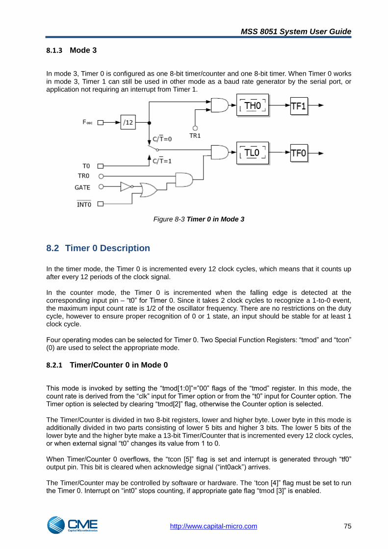
MSS 8051 System User Guide
http://www.capital-micro.com 75
8.1.3 Mode 3
In mode 3, Timer 0 is configured as one 8-bit timer/counter and one 8-bit timer. When Timer 0 works in mode 3, Timer 1 can still be used in other mode as a baud rate generator by the serial port, or application not requiring an interrupt from Timer 1.
Figure 8-3 Timer 0 in Mode 3
8.2 Timer 0 Description
In the timer mode, the Timer 0 is incremented every 12 clock cycles, which means that it counts up after every 12 periods of the clock signal. In the counter mode, the Timer 0 is incremented when the falling edge is detected at the corresponding input pin – ―t0‖ for Timer 0. Since it takes 2 clock cycles to recognize a 1-to-0 event, the maximum input count rate is 1/2 of the oscillator frequency. There are no restrictions on the duty cycle, however to ensure proper recognition of 0 or 1 state, an input should be stable for at least 1 clock cycle. Four operating modes can be selected for Timer 0. Two Special Function Registers: ―tmod‖ and ―tcon‖ (0) are used to select the appropriate mode.
8.2.1 Timer/Counter 0 in Mode 0
This mode is invoked by setting the ―tmod[1:0]‖=‖00‖ flags of the ―tmod‖ register. In this mode, the count rate is derived from the ―clk‖ input for Timer option or from the ―t0‖ input for Counter option. The Timer option is selected by clearing ―tmod[2]‖ flag, otherwise the Counter option is selected. The Timer/Counter is divided in two 8-bit registers, lower and higher byte. Lower byte in this mode is additionally divided in two parts consisting of lower 5 bits and higher 3 bits. The lower 5 bits of the lower byte and the higher byte make a 13-bit Timer/Counter that is incremented every 12 clock cycles, or when external signal ―t0‖ changes its value from 1 to 0. When Timer/Counter 0 overflows, the ―tcon [5]‖ flag is set and interrupt is generated through ―tf0‖ output pin. This bit is cleared when acknowledge signal (―int0ack‖) arrives. The Timer/Counter may be controlled by software or hardware. The ‗tcon [4]‖ flag must be set to run the Timer 0. Interrupt on ―int0‖ stops counting, if appropriate gate flag ―tmod [3]‖ is enabled.
MSS 8051 System User Guide
http://www.capital-micro.com 76
8.2.2 Timer/Counter 0 in Mode 1
This mode is invoked by setting the ―tmod [1:0]‖=‖01‖ flags of the ―tmod‖ register. This mode differs from Mode 0 only in that the lower byte is not divided in 5-bit and 3-bit parts, but the whole lower byte works as a counter. The Timer/Counter 0 is a 16 bit counter in mode 1.
8.2.3 Timer/Counter 0 in Mode 2
This mode is invoked by setting the ―tmod [1:0]‖=‖10‖ flags of the ―tmod‖ register. In this mode, the count rate is derived from the ―clk‖ input for Timer option or from the ―t0‖ input for Counter option. The Timer option is selected by clearing ―tmod [2]‖ flag, otherwise the Counter option is selected. In this mode only lower byte (―tl0‖) is incremented every 12 clock cycles or when external signal ―t0‖ changes its value from 1 to 0. In this mode the Timer/Counter works as an 8-bit reload timer/counter. When lower byte of Timer/Counter overflows, the ―tcon[5]‖ flag is set and interrupt is generated through ―tf0‖ output pin. This bit is cleared when acknowledge signal (―int0ack‖) arrives. Additionally, when the overflow occurs the new value is fetched from higher byte (―th0‖) to lower byte (―tl0‖). The Timer/Counter may be controlled by software or hardware. The ―tcon [4]‖ flag must be set to run the Timer 0. Interrupt on ―int0‖ stops counting, if appropriate gate flag ―tmod [3]‖ is enabled.
8.2.4 Timer/Counter 0 in Mode 3
This mode is invoked by setting the ―tmod [1:0]‖=11 flag of ―tmod‖ register. In this mode, the count rate for lower byte is derived from the ―clk‖ input for Timer option or from the ―t0‖ input for Counter option, but the count rate for higher byte is only derived from the ―clk‖. The Timer option is selected by clearing ―tmod [2]‖ flag; otherwise the Counter option is selected. In this mode the lower byte (―tl0‖) is incremented every 12 clock cycles or when external signal ―t0‖ changes its value from 1 to 0. The higher byte (―th0‖) is incremented every 12 clock cycles. When the lower byte of Timer/Counter overflows, the ―tcon [5]‖ flag is set and interrupt is generated through ―tf0‖ output pin. When the higher byte overflows, the ―tcon [7]‖ flag is set and interrupt is generated through ―tf1‖ output pin. These bits are cleared when appropriate acknowledge signals (―int0ack‖, ―int1ack‖) arrive, respectively. In this mode the lower byte of Timer/Counter 0 is controlled by ‗tcon[4]‖ flag which must be set to enable Timer operation, and by the ―int0‖ input which stops counting when forced to 0 while the ―tmod[3]‖ flag is set. The higher byte is controlled only by ―tcon [6]‖ flag which enables counting when set.

MSS 8051 System User Guide
http://www.capital-micro.com 77
9 Timer1
Timer 1 is a 16-bit register that can be configured for counter or timer operations. It can be accessed as SFRs: ―th1‖, ―tl1‖ (Timer1 – TH1, TL1).
9.1 Block diagram
9.1.1 Mode 0 and Mode 1
In mode 0, Timer 1 is configured as a 13-bit register (‖tl1‖ = 5 bits,‖th1‖ = 8 bits). The upper 3 bits of‖tl1‖ are unchanged and should be ignored. In mode 1 Timer 1 is configured as a 16- bit register.
Figure 9-1 Timer 1 in Mode 0 and 1
9.1.2 Mode 2
In this mode the Timer1 is configured as an 8-bit register with auto-reload.
Figure 9-2 Timer 1 in Mode 2
9.1.3 Mode 3
In mode 3 Timer 1 is stopped.
MSS 8051 System User Guide
http://www.capital-micro.com 78
9.2 Timer 1 Description
In the timer mode, the Timer 1 is incremented every 12 clock cycles, which means that it counts up after every 12 periods of the clock signal. In the counter mode, the Timer 1 is incremented when the falling edge is detected at the corresponding input pin – ―t1‖ for Timer 1. Since it takes 2 clock cycles to recognize a 1-to-0 event, the maximum input count rate is 1/2 of the oscillator frequency. There are no restrictions on the duty cycle, however to ensure proper recognition of 0 or 1 state, an input should be stable for at least 1 clock cycle. Four operating modes can be selected for Timer 1. Two Special Function Registers: ―tmod‖ and ―tcon‖ (0) are used to select the appropriate mode.
9.2.1 Timer/Counter 1 in Mode 0
This mode is invoked by setting the ―tmod [5:4]‖=‖00‖ flags of the ―tmod‖ register (see Table 4-11). In this mode, the count rate is derived from the ―clk‖ input for Timer option or from the ―t1‖ input for Counter option. The Timer option is selected by clearing ―tmod[6]‖ flag, otherwise the Counter option is selected. The Timer/Counter 1 is divided into two 8 bit registers, lower and higher byte. Lower byte in this mode is additionally divided in two parts consisting of lower 5 bits and higher 3 bits. Lower 5 bits from lower byte and higher byte make the Timer/Counter 1 a 13 bit counter that is incremented every 12 clock cycles or when external signal ―t1‖ changes its value from 1 to 0. When Timer/Counter 1 overflows, the ―tcon [7]‖ flag is set and interrupt is generated through ―tf1‖ output pin. This bit is cleared when acknowledge signal (―int1ack‖) arrives. The Timer/Counter 1 may be controlled by software or hardware. The ‗tcon [6]‖ flag must be set to run the Timer 1. Interrupt on ―int1‖ stops counting, if appropriate gate flag ―tmod [7]‖ is enabled.
9.2.2 Timer/Counter 1 in Mode 1
This mode is invoked by setting the ―tmod [5:4]‖=‖01‖ flags of the ―tmod‖ register (see Table 4-11). This mode differs from Mode 0 only in that the lower byte is not divided in 5-bit and 3-bit parts, but the whole lower byte works as a counter. The Timer/Counter 1 is a 16 bit counter in mode 1.
9.2.3 Timer/Counter 1 in Mode 2
This mode is invoked by setting the ―tmod[5:4]‖=‖10‖ flags of the ―tmod‖ register (see Table 4-11). In this mode, the count rate is derived from the ―clk‖ input for Timer option or from the ―t1‖ input for Counter option. The Timer option is selected by clearing the ―tmod[6]‖ flag, otherwise the Counter option is selected. In this mode the Timer/Counter works as an 8-bit reload timer/counter. Only lower byte (―tl1‖) is incremented every 12 clock cycles or when external signal ―t1‖ changes its value from 1 to 0. When lower byte of Timer/Counter overflows, the ―tcon[7]‖ flag is set and interrupt is generated through ―tf1‖ output pin. This bit is cleared when acknowledge signal (―int1ack‖) arrives. Additionally when the overflow occurs, the new value is fetched from higher byte (―th1‖) to lower byte (―tl1‖). The Timer/Counter may be controlled by software or hardware. The ―tcon[6]‖ flag must be set to run the Timer 1. Interrupt on ―int1‖ stops counting, if appropriate gate flag ―tmod[7]‖ is enabled.
MSS 8051 System User Guide
http://www.capital-micro.com 79
9.2.4 Timer/Counter 1 in Mode 3
This mode is invoked by setting the ―tmod[5:4]‖=11 flag of ―tmod‖ register (see Table 4-11). In this mode the Timer/Counter 1 is disabled (only Timer/Counter 0 can operate in mode 3).

MSS 8051 System User Guide
http://www.capital-micro.com 80
10 Timer2
Timer 2 can be configured for both counter or timer operations, and the Compare/Capture Unit which is a sub-component of Timer2.
10.1 Block diagram
Figure 10-1 Timer 2 Block Diagram
10.2 Timer 2 Description
The Timer 2 can operate as timer, event counter, or gated timer.
10.2.1 Timer mode
This mode is invoked by setting the ―t2i0‖=1 and ―t2i1‖=0 flags of ―t2con‖ register (See Table 4-13). In this mode, the count rate is derived from the ―clk‖ input. The Timer 2 is incremented every 12 or 24 clock cycles depending on the 2:1 prescaler. The prescaler mode is selected by bit ―t2ps‖ of ―t2con‖ register (See Table 4-13). When ―t2ps‖=0, the timer counts up every 12 clock cycles, otherwise every 24 cycles.
10.2.2 Event counter mode
This mode is invoked by setting the ―t2i0‖=0 and ―t2i1‖=1 flags of ―t2con‖ register (See Table 4-13). In this mode the Timer 2 is incremented when external signal ―t2‖ changes its value from 1 to 0. The ―t2‖ input is sampled at every rising edge of the clock. The Timer 2 is incremented in the cycle following the one in which the transition was detected. The maximum count rate is ½ of the clock frequency.
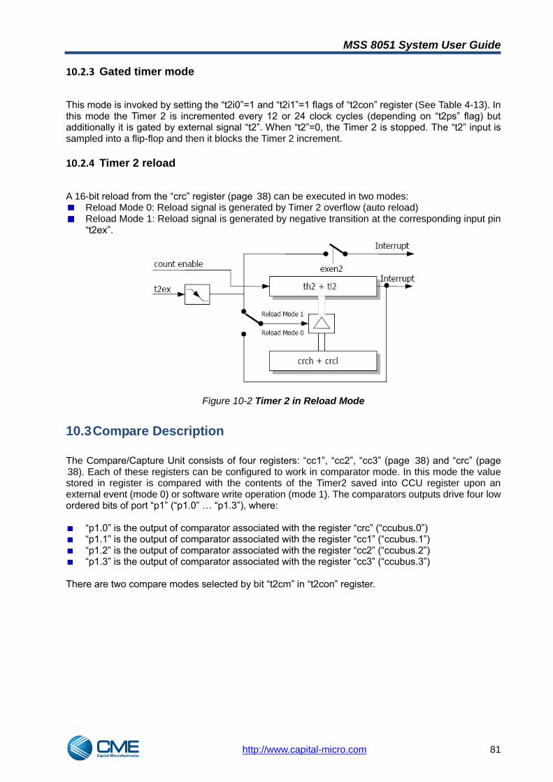
MSS 8051 System User Guide
http://www.capital-micro.com 81
10.2.3 Gated timer mode
This mode is invoked by setting the ―t2i0‖=1 and ―t2i1‖=1 flags of ―t2con‖ register (See Table 4-13). In this mode the Timer 2 is incremented every 12 or 24 clock cycles (depending on ―t2ps‖ flag) but additionally it is gated by external signal ―t2‖. When ―t2‖=0, the Timer 2 is stopped. The ―t2‖ input is sampled into a flip-flop and then it blocks the Timer 2 increment.
10.2.4 Timer 2 reload
A 16-bit reload from the ―crc‖ register (page 31H38) can be executed in two modes: Reload Mode 0: Reload signal is generated by Timer 2 overflow (auto reload) Reload Mode 1: Reload signal is generated by negative transition at the corresponding input pin
―t2ex‖.
Figure 10-2 Timer 2 in Reload Mode
10.3 Compare Description
The Compare/Capture Unit consists of four registers: ―cc1‖, ―cc2‖, ―cc3‖ (page 29H38) and ―crc‖ (page 30H38). Each of these registers can be configured to work in comparator mode. In this mode the value stored in register is compared with the contents of the Timer2 saved into CCU register upon an external event (mode 0) or software write operation (mode 1). The comparators outputs drive four low ordered bits of port ―p1‖ (―p1.0‖ … ―p1.3‖), where:
―p1.0‖ is the output of comparator associated with the register ―crc‖ (―ccubus.0‖) ―p1.1‖ is the output of comparator associated with the register ―cc1‖ (―ccubus.1‖) ―p1.2‖ is the output of comparator associated with the register ―cc2‖ (―ccubus.2‖) ―p1.3‖ is the output of comparator associated with the register ―cc3‖ (―ccubus.3‖)
There are two compare modes selected by bit ―t2cm‖ in ―t2con‖ register.
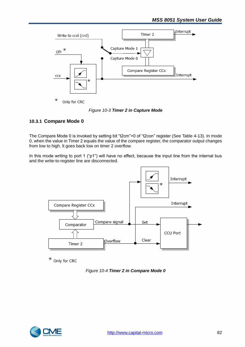
MSS 8051 System User Guide
http://www.capital-micro.com 82
Figure 10-3 Timer 2 in Capture Mode
10.3.1 Compare Mode 0
The Compare Mode 0 is invoked by setting bit ―t2cm‖=0 of ―t2con‖ register (See Table 4-13). In mode 0, when the value in Timer 2 equals the value of the compare register, the comparator output changes from low to high. lt goes back low on timer 2 overflow. In this mode writing to port 1 (―p1‖) will have no effect, because the input line from the internal bus and the write-to-register line are disconnected.
Figure 10-4 Timer 2 in Compare Mode 0
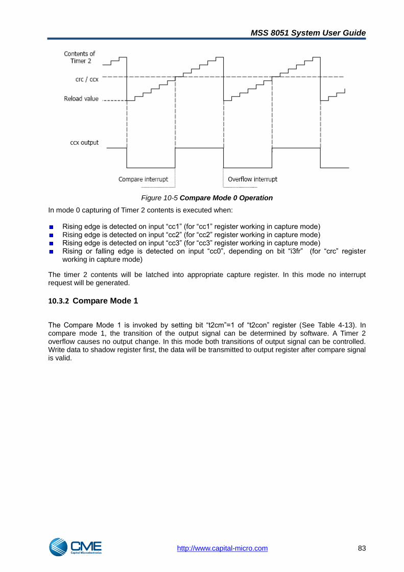
MSS 8051 System User Guide
http://www.capital-micro.com 83
Figure 10-5 Compare Mode 0 Operation
In mode 0 capturing of Timer 2 contents is executed when:
Rising edge is detected on input ―cc1‖ (for ―cc1‖ register working in capture mode) Rising edge is detected on input ―cc2‖ (for ―cc2‖ register working in capture mode) Rising edge is detected on input ―cc3‖ (for ―cc3‖ register working in capture mode) Rising or falling edge is detected on input ―cc0‖, depending on bit ―i3fr‖ (for ―crc‖ register
working in capture mode)
The timer 2 contents will be latched into appropriate capture register. In this mode no interrupt request will be generated.
10.3.2 Compare Mode 1
The Compare Mode 1 is invoked by setting bit ―t2cm‖=1 of ―t2con‖ register (See Table 4-13). In compare mode 1, the transition of the output signal can be determined by software. A Timer 2 overflow causes no output change. In this mode both transitions of output signal can be controlled. Write data to shadow register first, the data will be transmitted to output register after compare signal is valid.
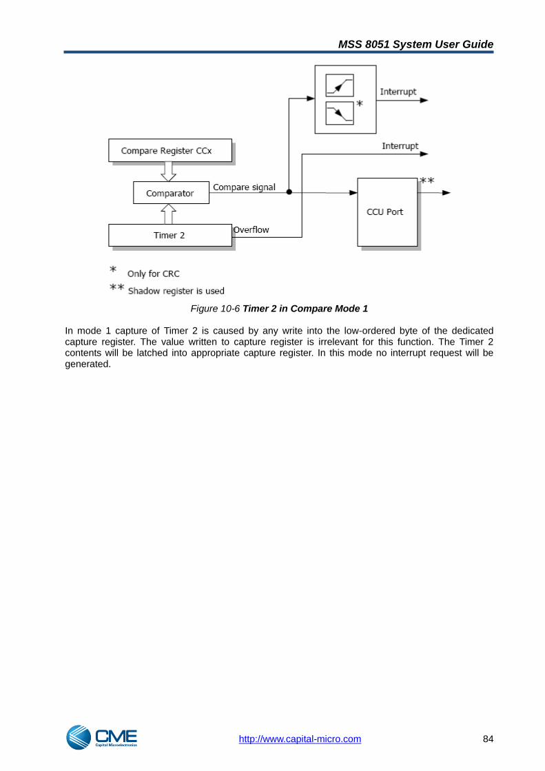
MSS 8051 System User Guide
http://www.capital-micro.com 84
Figure 10-6 Timer 2 in Compare Mode 1 In mode 1 capture of Timer 2 is caused by any write into the low-ordered byte of the dedicated capture register. The value written to capture register is irrelevant for this function. The Timer 2 contents will be latched into appropriate capture register. In this mode no interrupt request will be generated.

MSS 8051 System User Guide
http://www.capital-micro.com 85
11 USART0(Serial0)
The Serial0 provides a flexible full-duplex synchronous/asynchronous receiver/transmitter. It can operate in four modes (one synchronous and three asynchronous). The Serial0 is buffered at the receive side, i.e. it can receive new data while the previously received is not damaged in the receive register until the completion of the 2nd transfer. The Serial0 is fully compatible with the standard 8051 serial port.
11.1 Block diagram
Figure 11-1 Serial0 block diagram
11.2 Description
11.2.1 Baud Rate Generation
The Serial Port 0 Baud Rate Generation
Figure 11-2 Serial0 Baud Rate Generation Diagram

MSS 8051 System User Guide
http://www.capital-micro.com 86
11.2.2 Operating Mode
USART0 supports 4 operating modes.
(1) Mode 0
In mode 0, USART0 operates as synchronous transmitter/receiver. The "txd0" outputs the shift clock. The ―rxd0o‖ outputs data and the ―rxd0i‖ inputs data. 8 bits are transmitted with LSB first. The baud rate is fixed at 1/12 of the main clock frequency. Reception is started by setting the―ren0‖ = 1 flag ―s0con‖ register, and clearing the ―ri0‖ flag. Transmission is started by writing data to ―s0buf‖ register.
Figure 11-3 Serial0 Transmission in Mode 0
Figure 11-4 Serial0 Reception in Mode 0
(2) Mode 1
In mode 1, USART0 operates as asynchronous transmitter/receiver with 8 data bits and programmable baud rate. Depending on the setting of ―bd‖ bit of ―adcon‖ register (page 49H47), either Timer 1 overflow or ―s0relh‖, ―s0rell‖ baud rate generator is used. Additionally the baud rate can be doubled with the use of the ―smod‖ bit of the ―pcon‖ register. Transmission is started by writing to the ―s0buf‖ register. The ―txd0‖ pin outputs data. The first bit transmitted is a start bit (always 0), then 8 bits of data proceed, after which a stop bit (always 1) is transmitted. The ―rxd0i‖ pin inputs data. When reception starts, USART0 synchronizes with the falling edge detected at pin ―rxd0i‖. Input data are available after completion of the reception in the ―s0buf‖ register, and the value of stop bit is available as the ―rb80‖ flag in the ―s0con‖ register. During the reception, the ―s0buf‖ and ―rb80‖ remain unchanged until the completion.
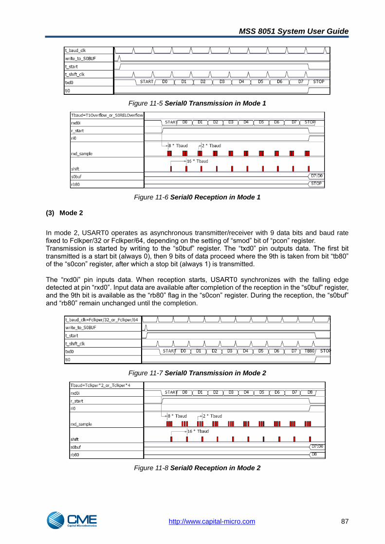
MSS 8051 System User Guide
http://www.capital-micro.com 87
Figure 11-5 Serial0 Transmission in Mode 1
Figure 11-6 Serial0 Reception in Mode 1
(3) Mode 2
In mode 2, USART0 operates as asynchronous transmitter/receiver with 9 data bits and baud rate fixed to Fclkper/32 or Fclkper/64, depending on the setting of ―smod‖ bit of ―pcon‖ register. Transmission is started by writing to the ―s0buf‖ register. The ―txd0‖ pin outputs data. The first bit transmitted is a start bit (always 0), then 9 bits of data proceed where the 9th is taken from bit ―tb80‖ of the ―s0con‖ register, after which a stop bit (always 1) is transmitted. The ―rxd0i‖ pin inputs data. When reception starts, USART0 synchronizes with the falling edge detected at pin ―rxd0‖. Input data are available after completion of the reception in the ―s0buf‖ register, and the 9th bit is available as the ―rb80‖ flag in the ―s0con‖ register. During the reception, the ―s0buf‖ and ―rb80‖ remain unchanged until the completion.
Figure 11-7 Serial0 Transmission in Mode 2
Figure 11-8 Serial0 Reception in Mode 2

MSS 8051 System User Guide
http://www.capital-micro.com 88
(4) Mode 3
The only difference between Mode 2 and Mode 3 is that in Mode 3 either internal baud rate generator or Timer 1 can be used to specify the baud rate.
Figure 11-9 Serial0 Transmission in Mode 3
Figure 11-10 Serial0 Reception in Mode 3
11.2.3 USART0 Multiprocessor Communication
The feature of receiving 9 bits in Modes 2 and 3 of Serial Interface 0 can be used for multiprocessor communication. When the ―sm20‖ bit of the ―s0con‖ register is set, the receive interrupt is generated only when the 9th received bit (―rb80‖ of ―s0con‖) is 1. Otherwise, no interrupt is generated upon reception. To utilize this feature to multiprocessor communication, the slave processors have their ―sm20‖ bit set to 1. The master processor transmits the slave‘s address, with the 9th bit set to 1, causing reception interrupt in all of the slaves. The slave processors‘ software compares the received byte with their network address. If there is a match, the addressed slave clears its ―sm20‖ flag and the rest of the message is transmitted from the master with the 9th bit set to 0. The other slaves keep their ―sm20‖ set to 1 so that they ignore the rest of the message sent by the master.
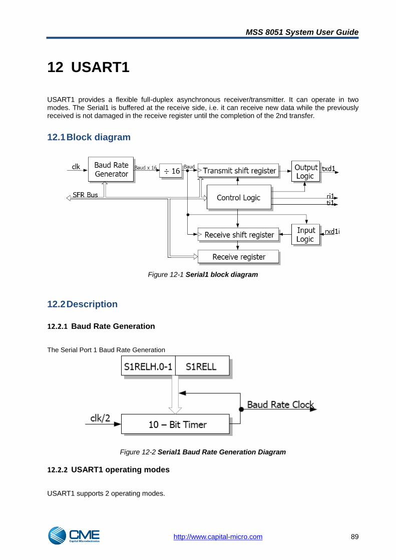
MSS 8051 System User Guide
http://www.capital-micro.com 89
12 USART1
USART1 provides a flexible full-duplex asynchronous receiver/transmitter. It can operate in two modes. The Serial1 is buffered at the receive side, i.e. it can receive new data while the previously received is not damaged in the receive register until the completion of the 2nd transfer.
12.1 Block diagram
Figure 12-1 Serial1 block diagram
12.2 Description
12.2.1 Baud Rate Generation
The Serial Port 1 Baud Rate Generation
Figure 12-2 Serial1 Baud Rate Generation Diagram
12.2.2 USART1 operating modes
USART1 supports 2 operating modes.

MSS 8051 System User Guide
http://www.capital-micro.com 90
(1) Mode A
In mode A, USART1 operates as asynchronous transmitter/receiver with 9 data bits and programmable baud rate. The ―s1relh‖, ―s1rell‖ baud rate generator is used to synchronize input and output transfers. The baud rate of USART1 cannot be modified using the ―smod‖ bit of the ―pcon‖ register. Transmission is started by writing to the ―s1buf‖ register. The ―txd1‖ pin outputs data. The first bit transmitted is a start bit (always 0), then 9 bits of data proceed where the 9th bit is taken from bit ―tb81‖ of the ―s1con‖ register, after which a stop bit (always 1) is transmitted. The ―rxd1i‖ pin inputs data. When reception starts, USART1 synchronizes with the falling edge detected at pin ―rxd1i‖. Input data are available after completion of the reception in the ―s1buf‖ register, and the 9th bit is available as the ―rb81‖ flag in the ―s1con‖ register (See Table 4-18). During the reception, the ―s1buf‖ and ―rb81‖ remain unchanged until the completion.
Figure 12-3 Serial1 Transmission in Mode A
Figure 12-4 Serial1 Reception in Mode A
(2) Mode B
In mode B, USART1 operates as asynchronous transmitter/receiver with 8 data bits and programmable baud rate. The ―s1relh‖, ―s1rell‖ baud rate generator is used to synchronize input and output transfers. The baud rate cannot be modified using the ―smod‖ bit of the ―pcon‖ register. Transmission is started by writing to the ―s1buf‖ register. The ―txd1‖ pin outputs data. The first bit transmitted is a start bit (always 0), then 8 bits of data proceed, after which a stop bit (always 1) is transmitted. The ―rxd1i‖ pin inputs data. When reception starts, USART1 synchronizes with the falling edge detected at pin ―rxd1i‖. Input data are available after completion of the reception in the ―s1buf‖ register, and the value of stop bit is available as the ―rb81‖ flag in the ―s1con‖ register (See Table 4-18). During the reception, the ―s1buf‖ and ―rb81‖ remain unchanged until the completion.
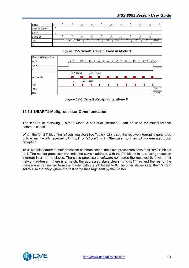
MSS 8051 System User Guide
http://www.capital-micro.com 91
Figure 12-5 Serial1 Transmission in Mode B
Figure 12-6 Serial1 Reception in Mode B
12.2.3 USART1 Multiprocessor Communication
The feature of receiving 9 bits in Mode A of Serial Interface 1 can be used for multiprocessor communication. When the ―sm21‖ bit of the ―s1con‖ register (See Table 4-18) is set, the receive interrupt is generated only when the 9th received bit (―rb81‖ of ―s1con‖) is 1. Otherwise, no interrupt is generated upon reception. To utilize this feature to multiprocessor communication, the slave processors have their ―sm21‖ bit set to 1. The master processor transmits the slave‘s address, with the 9th bit set to 1, causing reception interrupt in all of the slaves. The slave processors‘ software compares the received byte with their network address. If there is a match, the addressed slave clears its ―sm21‖ flag and the rest of the message is transmitted from the master with the 9th bit set to 0. The other slaves keep their ―sm21‖ set to 1 so that they ignore the rest of the message sent by the master.

MSS 8051 System User Guide
http://www.capital-micro.com 92
13 Watchdog Timer
The watchdog timer is a 15-bit counter that is incremented every 24 or 384 clock cycles. It is used to provide the system supervision in case of software or hardware upset. If the software is not able to refresh the Watchdog Timer after 786336 or 12581376 clock cycles (65ms or 1s when using 12MHz clock), an internal reset is generated.
13.1 Block Diagram
Figure 13-1 Serial1 block diagram
13.2 Description
The Watchdog Timer consists of 15-bit counter (not accessible as SFR), reload register ―wdtrel‖, prescalers by 2 and 16, and control logic. The count rate of the Watchdog Timer depends on the MSB of the ―wdtrel‖ register. When the ―wdtrel.7‖=1, the Watchdog Timer is incremented every 12*32=384 clock cycles, which makes the whole period to be 12*32*256*128=12582912 clock cycles long. When the ―wdtrel.7‖=0, the Watchdog Timer is incremented every 12*2=24 clock cycles, which makes the whole period to be 12*2*256*128= 786432 clock cycles long. When the ―wdt_tm‖ test mode input is set to 1, the count rate of the Watchdog Timer is clkper clock rate (all dividers – 1/12, 1/8, ½, 1/16 are omitted) to shorten the time required for the Watchdog to overflow (for verification purposes).
13.2.1 Start Procedure
There are two ways to start the watchdog. One method, called hardware automatic start, is based on examining the level of the ―swd‖ input signal during active external ―reset‖ signal. When ―swd‖ is high until the ―reset‖ goes low, the Watchdog Timer starts running automatically with default settings (all registers set to zero) after reset.
MSS 8051 System User Guide
http://www.capital-micro.com 93
The other way to start the Watchdog Timer is by software. The Watchdog Timer is started by setting ―swdt‖ flag of the ―ien1‖ register. Starting the Watchdog Timer by setting only ―swdt‖ flag does not reload the Watchdog Timer. Once started, the Watchdog Timer can only be stopped by forcing the ―swd‖ input pin inactive during the hardware reset using the ―reset‖ pin. When watchdog counter enters the state of 7FFCh, the internal reset is generated as the ―wdts‖ output is active. The ―wdts‖ flag of the ―ip0‖ register is also set upon the Watchdog Timer reset, while it is cleared upon external hardware ―reset‖ signal. The ―wdts‖ signal does not reset the Watchdog, which remains running. When it overflows from 7FFFh to 0000h, the ―wdts‖ output is deactivated, while the ―wdts‖ flag of ―ip0‖ register remains set to allow the software to determine whether the reset was caused by external input or by Watchdog timeout. The ―wdts‖ flag of the ―ip0‖ register can also be modified by software.
13.2.2 Refreshing the Watchdog Timer
The watchdog timer must be refreshed regularly to prevent reset request signal (―wdts‖) from becoming active. This requirement imposes obligation on the programmer to issue two followed instructions. The first instruction sets the ―wdt‖ bit of the ―ien0‖ register and the second one sets the ―swdt‖ flag of the ―ien1‖ register. The maximum allowed delay between setting the ―wdt‖ and ―swdt‖ is 1 instruction cycles (that means the instructions which set both flags are not separated with any other instruction). After that the ―wdt‖ flag is automatically cleared, which prevents the Watchdog Timer from being reloaded regardless of later ―swdt‖ flag setting. The 7 high-order bits of the Watchdog Timer are re-loaded with the contents of the ―wdtrel‖. The bigger the value of ―wdtrel‖ the shorter the period required to refresh the Watchdog Timer.

MSS 8051 System User Guide
http://www.capital-micro.com 94
14 Power Management and Reset Control Unit
The main purpose of the PMURSTCTRL subcomponent is to provide the R8051XC2 with two operation modes with limited power consumption (IDLE or STOP) and to generate the internal synchronous reset signal. The power down modes is implemented as two outputs controlling the behaviour of the off-core clock generator. The PMURSTCTRL generates output signals named ―clkcpuen‖ and ―clkperen‖ which should be externally used as gating control signals for clocks connected with appropriate R8051XC2 inputs (―clkcpu‖ and ―clkper‖, respectively). These signals serve as clock enable signals for R8051XC2 CPU and peripherals. The most of all registers and flip-flops in the R8051XC2 design are synchronously reset by high active internal ―rst‖ signal. External hardware reset or watchdog timer reset can activate this signal. High level on external ―reset‖ pin or watchdog reset request for at least two clock cycles while the ―clk‖ is running resets the device. The ―rst‖ signal is synchronized with the ―clkper‖ in the SYNCNEG module, then it is combined with the other reset requests from Watchdog, Software Reset module and the OCDS in the PMURSTCTRL, and again it is synchronized by one flip-flop in the SYNCNEG module. The Power Management Unit provides two power management modes: IDLE and STOP.
14.1 Power Managerment Description
14.1.1 Idle mode
Setting the ―idle‖ bit of ―pcon‖ register invokes the IDLE mode. In the IDLE mode clock for peripherals is running (the ―clkper_en‖=1, ―clkcpu_en‖=0). Power consumption drops because the CPU clock is stopped. The CPU can exit the IDLE state with any interrupt or reset.
14.1.2 Stop mode
Setting the ―stop‖ bit of ―pcon‖ register invokes the STOP mode. Both clocks for the CPU and peripherals are stopped in this mode (the ―clkper_en‖=0, ―clkcpu_en‖=0). The CPU can exit this state with an external interrupt (―int0‖ or ―int1‖) or reset. Internally generated interrupts (timer, serial port…) cannot be used since they require clock activity to operate. The ―clkcpu_en‖ output is dedicated to control the off-core gate on to the ―clkcpu‖ input. The ―clkper_en‖ output is dedicated to control the off-core gate on to the ―clkper‖ input.
14.2 Reset control Description
The external ―reset‖ input is sampled by two rising-edge triggered flip-flops in the SYNCNEG module. The main device synchronous reset ―rst‖ is activated three clock periods after hardware ―reset‖ is active. The ―rst‖ is active for minimum 2 clock cycles to allow the proper reset when Power Down mode is invoked. When the Watchdog Timer overflow occurs, the ―rst‖ is activated immediately.
MSS 8051 System User Guide
http://www.capital-micro.com 95
15 Port
The PORTS subcomponent is composed of four 8-bit registers that can be accessed as Special Function Registers: ―p0‖, ―p1‖, ―p2‖ and ―p3‖ while performing write or Read-Modify-Write instructions. The contents of these registers is reflected at the output ports: ―port0o‖, ―port1o‖, ―port2o‖ and ―port3o‖, respectively. The related inputs of the ―p0‖...‖p3‖ are sampled by the SYNCNEG module to filter-out the metastable states. The Read-Modify-Write access to the Ports is performed in the SFRMUX module, where either the contents of an output register (―port0‖..‖port3‖) or the sampled inputs (―port0ff‖..‖port3ff‖) are selected using the ―rmwinstr‖ signal. To ensure the 8051-like Ports, it is required for the corresponding inputs and outputs to be externally (off-core) connected using open-drain buffers.
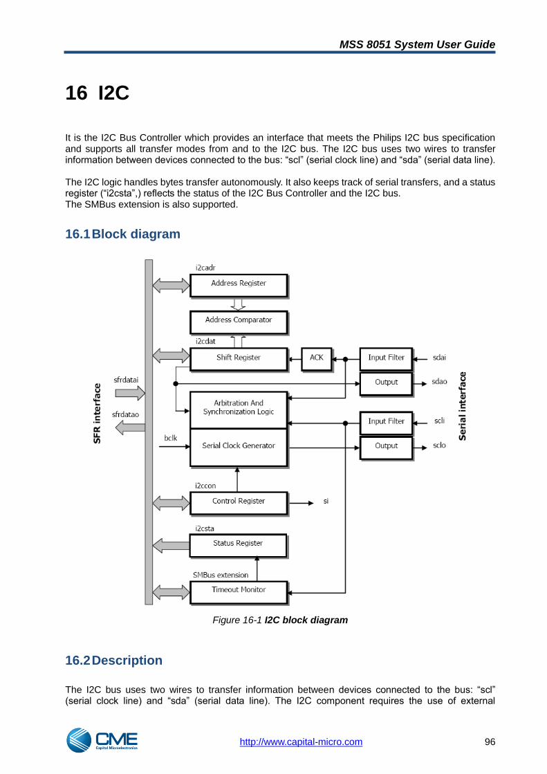
MSS 8051 System User Guide
http://www.capital-micro.com 96
16 I2C
It is the I2C Bus Controller which provides an interface that meets the Philips I2C bus specification and supports all transfer modes from and to the I2C bus. The I2C bus uses two wires to transfer information between devices connected to the bus: ―scl‖ (serial clock line) and ―sda‖ (serial data line). The I2C logic handles bytes transfer autonomously. It also keeps track of serial transfers, and a status register (―i2csta‖,) reflects the status of the I2C Bus Controller and the I2C bus. The SMBus extension is also supported.
16.1 Block diagram
Figure 16-1 I2C block diagram
16.2 Description
The I2C bus uses two wires to transfer information between devices connected to the bus: ―scl‖ (serial clock line) and ―sda‖ (serial data line). The I2C component requires the use of external
MSS 8051 System User Guide
http://www.capital-micro.com 97
open-drain buffers since it has only unidirectional ports. The ―sda‖ and ―scl‖ lines referred further are the actual I2C bus signals, while the I2C component is connected to them with the use of open-drains (―sdao‖ as output and ―sdai‖ as input, ―sclo‖ as output and ―scli‖ as input). Each device connected to the bus is software addressable by a unique address. The I2C is a true multi-master bus including collision detection and arbitration to prevent data corruption if two or more masters simultaneously initiate data transfer. The filtering logic rejects spikes on the bus data line to preserve data integrity.
16.2.1 Operating Modes
The I2C component performs 8-bit oriented; bi-directional data transfers up to 100 kbit/s in the standard mode or up to 400 kbit/s in the fast mode and may operate in the following four modes:
(1) Master Transmitter Mode:
Serial data output through ―sdao‖ while ―sclo‖ outputs the serial clock.
(2) Master Receiver Mode:
Serial data is received via ―sdai‖ while ―sclo‖ outputs the serial clock.
(3) Slave Receiver Mode
Serial data and the serial clock are received through ―sdai‖ and ―scli‖.
(4) Slave Transmitter Mode
Serial data is transmitted via ―sdao‖ while the serial clock is input through ―scli‖.
16.2.2 Arbitration
In the master mode, the arbitration logic checks that every transmitted high state (‗1‘) on ―sdao‖ actually appears as high state (‗1‘) on the I2C bus ―sda‖. If another device on the bus overrides high and pulls the ―sda‖ line low (‗0‘), arbitration is lost and the I2C immediately changes from master transmitter to slave receiver.
16.2.3 Serial clock generator
This programmable clock pulse generator provides the ―scl‖ clock pulses when the I2C is in the master mode. The clock generator is suppressed when the I2C is in the slave mode. The function of the clock generator is controlled by bits ―cr0‖, ―cr1‖ and ―cr2‖ of ―i2ccon‖ register. The table below shows the possible rates of ―clko‖ in the master mode. The ―bclk‖ input referenced in the table is connected to the Timer 1 overflow output. That means the baud rate of the I2C can be controlled by the Timer 1.

MSS 8051 System User Guide
http://www.capital-micro.com 98
Table 16-1 I2C clock frequency bit settings
cr2 cr1 cr0 Bit frequency Clk divided by
6 MHz 12 MHz 16 MHz 24 MHz
0 0 0 23(KHz) 47(KHz) 63(KHz) 92(KHz) 256
0 0 1 27(KHz) 54(KHz) 71(KHz) 108(KHz) 224
0 1 0 31(KHz) 63(KHz) 83(KHz) 124(KHz) 192
0 1 1 37(KHz) 75(KHz) 100(KHz) 148(KHz) 160
1 0 0 6.25(KHz) 12.5(KHz) 17(KHz) 25(KHz) 960
1 0 1 50(KHz) 100(KHz) 133(KHz) 200(KHz) 120
1 1 0 100(KHz) 200(KHz) 266(KHz) 400(KHz) 60
1 1 1 ―bclk‖ input divided by 8
16.2.4 Address comparator
The received 7-bit slave address is compared with the I2C component own slave address. The own slave address can be programmed using the ―i2cadr‖ register. Also the first received byte is compared with the general call address (00H), depending on the ―gc‖ bit of ―i2cadr‖ register.If equality is found, the ―si‖ bit of the ―i2ccon‖ register is set and an interrupt is requested.
16.2.5 Interrupt Generation
The ―si― flag of the ―i2ccon‖ register is set by hardware when one of 25 out of 26 possible I2C states is entered. The only state that does not set the ―si‖ is state F8h, which indicates that no relevant state information is available. The ―si‖ flag must be cleared by software. In order to clear the ―si‖ bit, ‗0‘ must be written to this bit. Writing a ‗1‘ to si bit does not change value of the ―si‖. The I2C interrupt share the same interrupt vectors works as external interrupt 7. The ―si‖ signal is OR-ed with the External Interrupt 7 edge flag, before it comes into the Interrupt Controller (ISR). To determine the actual source of that interrupt, the ―si‖ flag has to be investigated by the interrupt service routine. Since the External Interrupt 7 flag is automatically cleared after vectoring to the service subroutine, only the state of the ―si‖ flag brings the information of the actual source of the interrupt.
16.2.6 Special Function Registers
The microprocessor interfaces to the I2C component via the following four special function registers: ―i2ccon‖ (control register, below), ―i2csta‖ (status register, below), ―i2cdat‖ (data register, below) and ―i2cadr‖ (own slave address registe). The ―i2cadr‖ register contains the Own Slave Address of the I2C component, and the ―gc‖ flag which enables the recognition of a general call address. The ―i2ccon‖ register contains the global I2C enable bit ―ens1‖, clock rate setting bits (―cr0‖, ―cr1‖, ―cr2‖). It also provides flags to initiate sending START or STOP conditions to the I2C bus (―sta‖, ―sto‖ bits), a flag controlling the ACK bit in I2C transmission after receiving own slave address or general call address or after receiving data either in master or slave mode (―aa‖ – assert acknowledge flag). Finally the ―i2ccon‖ provides the interrupt request flag ―si‖ which is set by hardware when a change of the main controlling FSM is detected. See the ―i2csta‖ register description for FSM details. The ―i2cdat‖ register contains a byte to be transmitted through I2C bus or a byte which has just been received through I2C bus. The ―i2cdat‖ register is not shadowed or double buffered so the MCU
MSS 8051 System User Guide
http://www.capital-micro.com 99
would only read it when an I2C interrupt occurs. The ―i2csta‖ register reflects the state of the main FSM of the I2C component. The three least significant bits of this register are always zero. There are 26 possible status codes, which are presented in 41HTable 16-2 I2C Status in Master Transmitter Mode to Table 16-6 I2C Status - miscellaneous states. When one of the 25 out of 26 possible I2C FSM states is entered, an interrupt is requested. The only state that does not generate an interrupt is the F8h state. To clear the flag, ‗0‘ must be written in ―si‖ by software, while writing ‗1‘ can not change the value in ―si‖ at all. In the table below, referring to ―SLA‖ means slave address, ―R‖ means R/W bit=1 transferred together with the slave address, ―W‖ means R/W bit=0 transferred together with the slave address.
Table 16-2 I2C Status in Master Transmitter Mode
Status code
Status of the I2C Application software
response Next action taken by the I
2C hardware
to/from I2CDAT
to I2CCON
sta sto si aa
08H START condition has been transmitted
Load SLA+W
X 0 0 X SLA+W will be transmitted ACK will be received
10H Repeated START condition has been transmitted
Load SLA+W
X 0 0 X As above
or Load SLA+R
X 0 0 X SLA+R will be transmitted;I2C
will be switched to MST/REC mode
18H SLA+W has been transmitted; ACK has been received
Load data byte
0 0 0 X Data byte will be transmitted; ACK will be received
or no action
1 0 0 X Repeated START will be ransmitted;
or no action
0 1 0 X STOP condition will be transmitted; the ―sto‖ flag will be reset
or no action
1 1 0 X STOP condition followed by a START condition will be transmitted; the ―sto‖ flag will be reset
20H SLA+W has been transmitted; ―not ACK‖ has been received
Load data byte
0 0 0 X Data byte will be transmitted; ACK will be received
or no action
1 0 0 X Repeated START will be transmitted;
or no action
0 1 0 X STOP condition will be transmitted; the ―sto‖ flag will be reset
or no action
1 1 0 X STOP condition followed by a START condition will be transmitted; the ―sto‖ flag will be reset
28H Data byte in i2cdat has been transmitted; ACK has been received
Load data byte
0 0 0 X Data byte will be transmitted; ACK bit will be received
or no action
1 0 0 X Repeated START will be transmitted
or no action
0 1 0 X STOP condition will be transmitted; the ―sto‖ flag will be
MSS 8051 System User Guide
http://www.capital-micro.com 100
Status code
Status of the I2C Application software
response Next action taken by the I
2C hardware
to/from I2CDAT
to I2CCON
sta sto si aa
reset
or no action
1 1 0 X STOP condition followed by a START condition will be transmitted; sto flag will be reset
30H Data byte in i2cdat has been transmitted
Data byte 0 0 0 X Data byte will be transmitted; ACK will be received
or no action
1 0 0 X Repeated START will be transmitted;
or no action
0 1 0 X STOP condition will be transmitted; sto flag will be reset
or no action
1 1 0 X STOP condition followed by a START condition will be transmitted; sto flag will be reset
Table 16-3 I2C Status in Master Receiver Mode
Status code
Status of the I2C Application software
response Next action taken by the I
2C
hardware
to/from to i2CCON
I2CDAT sta sto si aa
08H START condition has been transmitted
Load SLA+R
X 0 0 X SLA+R will be transmitted; ACK will be received
10H Repeated START condition has been transmitted
Load SLA+R
X 0 0 X As above
or Load SLA+W
X 0 0 X SLA+W will be transmitted; I2C
will be switched to ―master transmitter‖ mode
40H SLA+R has been transmitted; ACK has been received
No action 0 0 0 0 Data byte will be received;
or no action
0 0 0 1 not ACK will be returned
Data byte will be received; ACK will be returned
48H SLA+R has been transmitted; ACK has been received
No action 1 0 0 X Repeated START condition will be transmitted
or no action
0 1 0 X STOP condition will be transmitted; the ―sto‖ flag will be reset
or no action
1 1 0 X STOP condition followed by START condition will be transmitted; the ―sto‖ flag will be reset
50H Data byte has been received; ACK has been returned
Read data byte
0 0 0 0 Data byte will be received; ―not ACK‖ will be returned
or read data byte
0 0 0 1 Data byte will be received; ACK will be returned
58H Data byte has been received; ACK has been returned
or Read data byte
1 0 0 X Repeated START condition will be transmitted

MSS 8051 System User Guide
http://www.capital-micro.com 101
Status code
Status of the I2C Application software
response Next action taken by the I
2C
hardware
to/from to i2CCON
I2CDAT sta sto si aa
or read data byte
0 1 0 X STOP condition will be transmitted; the ―sto‖ flag will be reset
or read data byte
1 1 0 X STOP condition followed by START condition will be transmitted; the ―sto‖ flag will be reset
Table 16-4 I2C Status in Slave Receiver Mode
Status code
Status of the I2C Application software
response Next action taken by the I
2C
hardware
to/from to i2CCON
I2CDAT sta sto si aa
60H Own SLA+W has been received; ACK has been returned
No action
X 0 0 0 Data byte will be received and ―not ACK‖ will be returned
or no action
X 0 0 1 Data byte will be received and ACK will be returned
68H Arbitration lost in SLA+R/W as master; own SLA+W has been received, ACK returned
or No action
X 0 0 0 Data byte will be received and ―not ACK‖ will be returned
or no action
X 0 0 1 Data byte will be received and ACK will be returned
70H General call address (00H) has been received; ACK has been returned
or No action
X 0 0 0 Data byte will be received and ―not ACK‖ will be returned
or no action
X 0 0 1 Data byte will be received and ACK will be returned
78H Arbitration lost in SLA+R/W as
No action
X 0 0 0 Data byte will be received and ―not ACK‖ will be returned
master; general call address has been received, ACK returned
or no action
X 0 0 1 Data byte will be received and ACK will be returned
80H Previously addressed with own SLV address; DATA has been received; ACK returned
Read data byte
X 0 0 0 Data byte will be received and ―not ACK‖ will be returned
or read data byte
X 0 0 1 Data byte will be received and ACK will be returned
88H Previously addressed with own SLA; DATA byte has been received; ―not ACK‖ returned
Read data byte
0 0 0 0 Switched to ―not addressed slave‖ mode; no recognition of own slave address or general call address
or read data byte
0 0 0 1 Switched to ―not addressed slave‖ mode; own slave address or general call address will be recognized
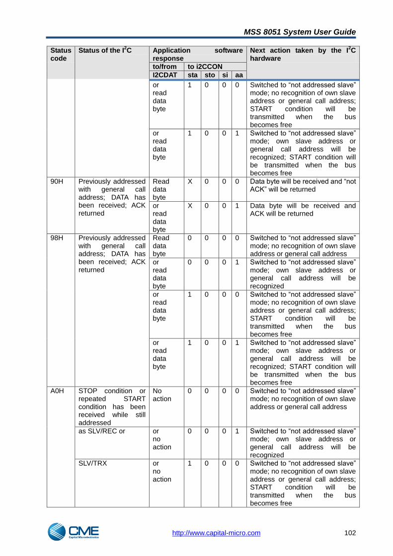
MSS 8051 System User Guide
http://www.capital-micro.com 102
Status code
Status of the I2C Application software
response Next action taken by the I
2C
hardware
to/from to i2CCON
I2CDAT sta sto si aa
or read data byte
1 0 0 0 Switched to ―not addressed slave‖ mode; no recognition of own slave address or general call address; START condition will be transmitted when the bus becomes free
or read data byte
1 0 0 1 Switched to ―not addressed slave‖ mode; own slave address or general call address will be recognized; START condition will be transmitted when the bus becomes free
90H Previously addressed with general call address; DATA has been received; ACK returned
Read data byte
X 0 0 0 Data byte will be received and ―not ACK‖ will be returned
or read data byte
X 0 0 1 Data byte will be received and ACK will be returned
98H Previously addressed with general call address; DATA has been received; ACK returned
Read data byte
0 0 0 0 Switched to ―not addressed slave‖ mode; no recognition of own slave address or general call address
or read data byte
0 0 0 1 Switched to ―not addressed slave‖ mode; own slave address or general call address will be recognized
or read data byte
1 0 0 0 Switched to ―not addressed slave‖ mode; no recognition of own slave address or general call address; START condition will be transmitted when the bus becomes free
or read data byte
1 0 0 1 Switched to ―not addressed slave‖ mode; own slave address or general call address will be recognized; START condition will be transmitted when the bus becomes free
A0H STOP condition or repeated START condition has been received while still addressed
No action
0 0 0 0 Switched to ―not addressed slave‖ mode; no recognition of own slave address or general call address
as SLV/REC or or no action
0 0 0 1 Switched to ―not addressed slave‖ mode; own slave address or general call address will be recognized
SLV/TRX or no action
1 0 0 0 Switched to ―not addressed slave‖ mode; no recognition of own slave address or general call address; START condition will be transmitted when the bus becomes free
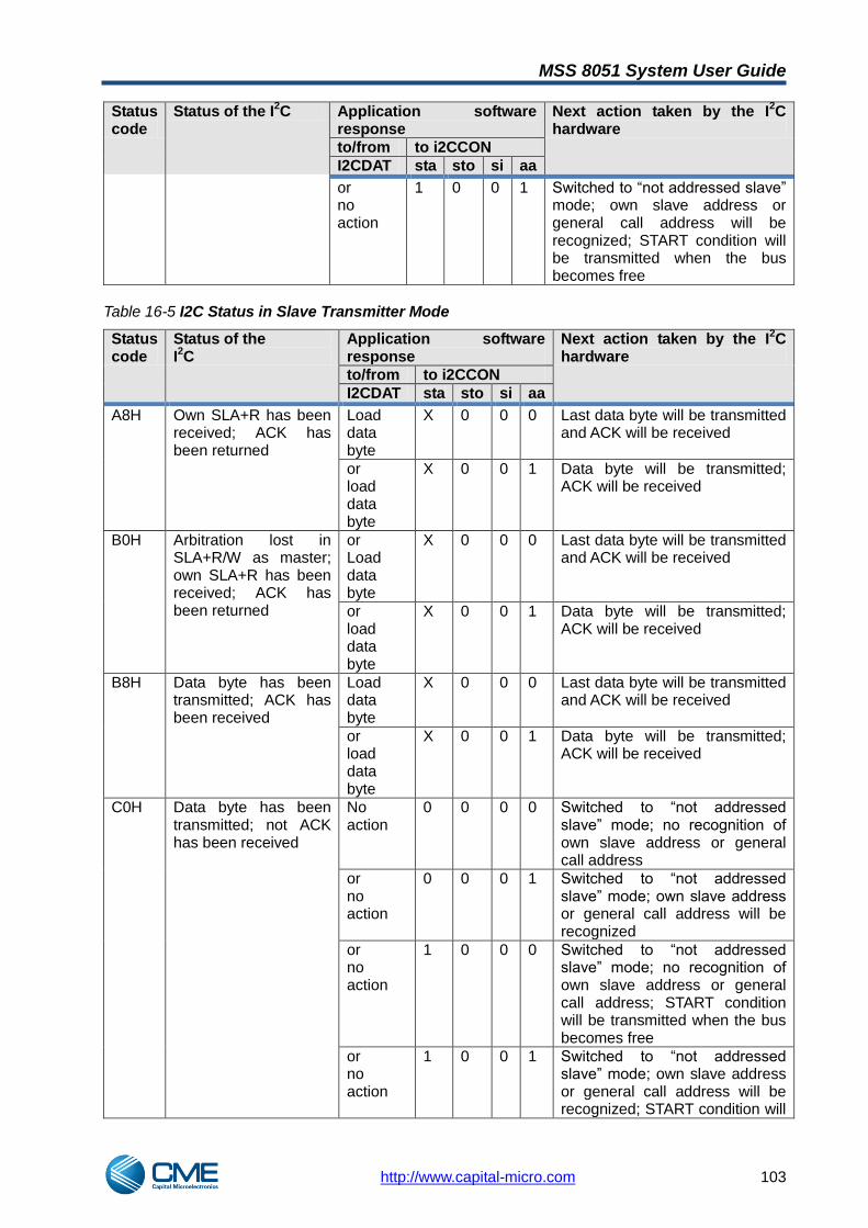
MSS 8051 System User Guide
http://www.capital-micro.com 103
Status code
Status of the I2C Application software
response Next action taken by the I
2C
hardware
to/from to i2CCON
I2CDAT sta sto si aa
or no action
1 0 0 1 Switched to ―not addressed slave‖ mode; own slave address or general call address will be recognized; START condition will be transmitted when the bus becomes free
Table 16-5 I2C Status in Slave Transmitter Mode
Status code
Status of the I2C
Application software response
Next action taken by the I2C
hardware
to/from to i2CCON
I2CDAT sta sto si aa
A8H Own SLA+R has been received; ACK has been returned
Load data byte
X 0 0 0 Last data byte will be transmitted and ACK will be received
or load data byte
X 0 0 1 Data byte will be transmitted; ACK will be received
B0H Arbitration lost in SLA+R/W as master; own SLA+R has been received; ACK has been returned
or Load data byte
X 0 0 0 Last data byte will be transmitted and ACK will be received
or load data byte
X 0 0 1 Data byte will be transmitted; ACK will be received
B8H Data byte has been transmitted; ACK has been received
Load data byte
X 0 0 0 Last data byte will be transmitted and ACK will be received
or load data byte
X 0 0 1 Data byte will be transmitted; ACK will be received
C0H Data byte has been transmitted; not ACK has been received
No action
0 0 0 0 Switched to ―not addressed slave‖ mode; no recognition of own slave address or general call address
or no action
0 0 0 1 Switched to ―not addressed slave‖ mode; own slave address or general call address will be recognized
or no action
1 0 0 0 Switched to ―not addressed slave‖ mode; no recognition of own slave address or general call address; START condition will be transmitted when the bus becomes free
or no action
1 0 0 1 Switched to ―not addressed slave‖ mode; own slave address or general call address will be recognized; START condition will

MSS 8051 System User Guide
http://www.capital-micro.com 104
Status code
Status of the I2C
Application software response
Next action taken by the I2C
hardware
to/from to i2CCON
I2CDAT sta sto si aa
be transmitted when the bus becomes free
C8H Last data byte has been transmitted; ACK has been received
No action
0 0 0 0 Switched to ―not addressed slave‖ mode; no recognition of own slave address or general call address
or no action
0 0 0 1 Switched to ―not addressed slave‖ mode; own slave address or general call address will be recognized
or no action
1 0 0 0 Switched to ―not addressed slave‖ mode; no recognition of own slave address or general call address; START condition will be transmitted when the bus becomes free
or no action
1 0 0 1 Switched to ―not addressed slave‖ mode; own slave address or general call address will be recognized; START condition will be transmitted when the bus becomes free
Table 16-6 I2C Status - miscellaneous states
Status code
Status of the I2C
Application software response
Next action taken by the I2C
hardware
to/from to i2CCON
I2CDAT sta sto si aa
38H Arbitration lost No action
0 0 0 x I2C bus will be released;
or no action
1 0 0 x A start condition will be transmitted when the bus becomes free (enter to a master mode)
F8H No relevant state information available; si=0
No action
No action Wait or proceed current transfer
00H Bus error during MST or selected slave modes
No action
0 1 0 X Only the internal hardware is affected in the ―master‖ or ―addressed slave‖ modes. In all cases, the bus is released and I
2C is switched to the
―not addressed slave‖ mode. The ―sto‖ flag is reset.
16.3 System Management Bus Extension
The System Management Bus (SMBus) protocol hardware implementation features:
Timeout detection (clock low timeout measurement) Tmext timeout detection (cumulative stretch clock cycles within one byte) Tsext timeout detection (cumulative stretch clock cycles between start and stop condition)

MSS 8051 System User Guide
http://www.capital-micro.com 105
The SMBus requires two additional registers: ―smb_sel‖ (located at 0xDE sfr addres) and ―smb_dst‖ (located at 0xDF sfr addres, see 2.4.54 ). They both form a read/write access port to the timeout registers. The ―smb_sel‖ is used to enable the SMBus feature (bit 7), and for selecting the SMBus internal timeout register being accessed through the other register as a data port. The ―smb_dst‖ register is used to read or write internal SMBus timeout register, which is selected by the ―smb_sel‖. Table 16-7 SMBus registers
smb_sel smb_dst Description
0xxxxxxx - Disable SMBus timeout features. 1xxxxxxx - Enable SMBus timeout features.
xxxxx000 TMEXT_L Select the least significant byte of Tmext register.
xxxxx001 TMEXT_H Select the most significant byte of Tmext register.
xxxxx010 TSEXT_L Select the least significant byte of Tsext register.
xxxxx011 TSEXT_H Select the most significant byte of Tsext register.
xxxxx100 TOUT_L Select the least significant byte of Tout register.
xxxxx101 TOUT_H Select the most significant byte of Tout register.
The value of SMBus timeout registers should be calculated according to the following formula:
Txxx = timeout[sec] * fclkper[Hz] / 1024
Example:
fclkper = 24 MHz
Tmext = 5ms -> TMEXT = 118 Tsext = 25ms -> TSEXT =
586 Tout = 35ms -> TOUT = 821
When the SMBus feature is enabled, the 3 least significant bits of the I2C status register hold the information about tiomeouts. Table 16-8 SMBus error status
I2C2STA Description
xxxxx000 No timeout errors. Xxxxxxx1
Tout timeout error.
Xxxxxx1
x Tsext timeout error.
xxxxx1xx Tmext timeout error.
MSS 8051 System User Guide
http://www.capital-micro.com 106
17 SPI
The SPI interface allows full-duplex, synchronous, serial communication between the MCU and peripherals, including other MCUs. It is obvious that the MCU and any peripherals must include SPI module. The module may be programmed to work as master or as slave device, with the following features:
Full duplex mode
Three wire synchronous transfers
Master or Slave mode
Seven SPI Master baud rates
Slave Clock rate up to Fclk/4
Serial clock with programmable polarity and phase
8-bit data transmitted Most Significant Bit (MSB) first, Least Significant Bit (LSB) last 8-bit Slave Select Output port to control external slave devices

MSS 8051 System User Guide
http://www.capital-micro.com 107
17.1 Block diagram
Figure 17-1 SPI Block Diagram
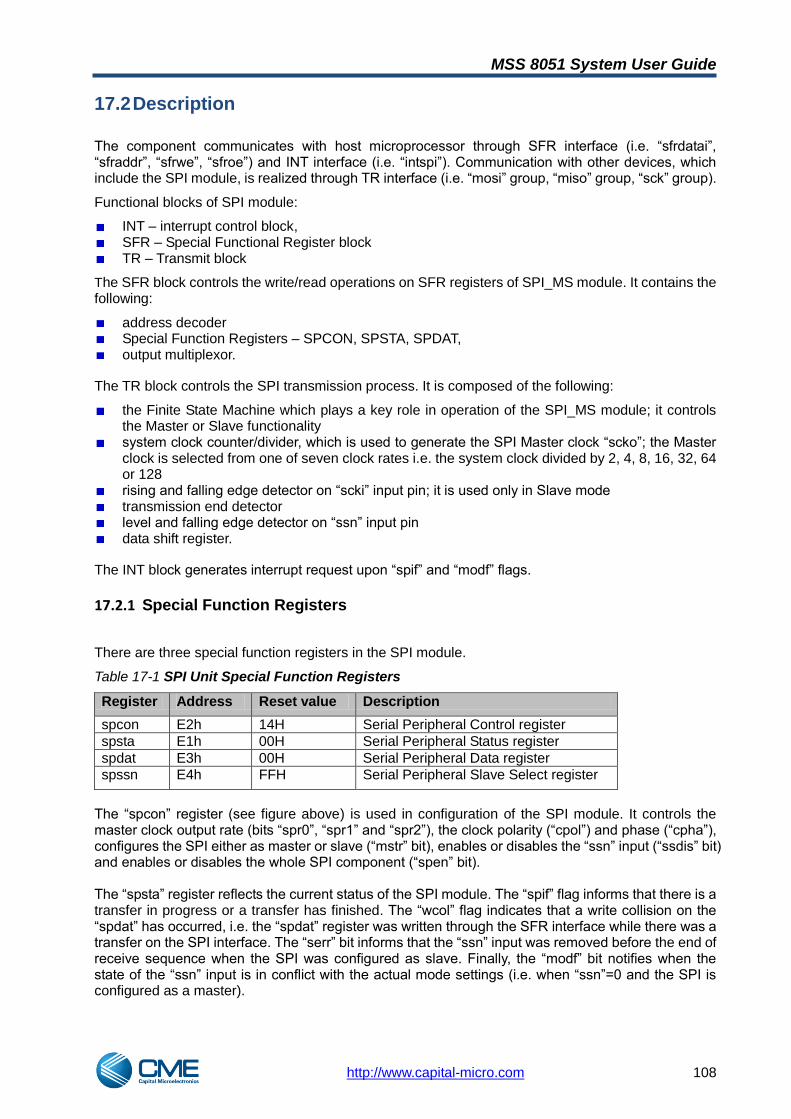
MSS 8051 System User Guide
http://www.capital-micro.com 108
17.2 Description
The component communicates with host microprocessor through SFR interface (i.e. ―sfrdatai‖, ―sfraddr‖, ―sfrwe‖, ―sfroe‖) and INT interface (i.e. ―intspi‖). Communication with other devices, which include the SPI module, is realized through TR interface (i.e. ―mosi‖ group, ―miso‖ group, ―sck‖ group).
Functional blocks of SPI module:
INT – interrupt control block,
SFR – Special Functional Register block
TR – Transmit block
The SFR block controls the write/read operations on SFR registers of SPI_MS module. It contains the following:
address decoder Special Function Registers – SPCON, SPSTA, SPDAT, output multiplexor.
The TR block controls the SPI transmission process. It is composed of the following:
the Finite State Machine which plays a key role in operation of the SPI_MS module; it controls the Master or Slave functionality
system clock counter/divider, which is used to generate the SPI Master clock ―scko‖; the Master clock is selected from one of seven clock rates i.e. the system clock divided by 2, 4, 8, 16, 32, 64 or 128
rising and falling edge detector on ―scki‖ input pin; it is used only in Slave mode transmission end detector level and falling edge detector on ―ssn‖ input pin data shift register.
The INT block generates interrupt request upon ―spif‖ and ―modf‖ flags.
17.2.1 Special Function Registers
There are three special function registers in the SPI module.
Table 17-1 SPI Unit Special Function Registers
Register Address Reset value Description
spcon E2h 14H Serial Peripheral Control register
spsta E1h 00H Serial Peripheral Status register
spdat E3h 00H Serial Peripheral Data register
spssn E4h FFH Serial Peripheral Slave Select register
The ―spcon‖ register (see figure abovef) is used in configuration of the SPI module. It controls the master clock output rate (bits ―spr0‖, ―spr1‖ and ―spr2‖), the clock polarity (―cpol‖) and phase (―cpha‖), configures the SPI either as master or slave (―mstr‖ bit), enables or disables the ―ssn‖ input (―ssdis‖ bit) and enables or disables the whole SPI component (―spen‖ bit). The ―spsta‖ register reflects the current status of the SPI module. The ―spif‖ flag informs that there is a transfer in progress or a transfer has finished. The ―wcol‖ flag indicates that a write collision on the ―spdat‖ has occurred, i.e. the ―spdat‖ register was written through the SFR interface while there was a transfer on the SPI interface. The ―serr‖ bit informs that the ―ssn‖ input was removed before the end of receive sequence when the SPI was configured as slave. Finally, the ―modf‖ bit notifies when the state of the ―ssn‖ input is in conflict with the actual mode settings (i.e. when ―ssn‖=0 and the SPI is configured as a master).

MSS 8051 System User Guide
http://www.capital-micro.com 109
The ―spdat‖ register is used during transmission process. Data from this register can be sent through the TR (Transmit/Receive) interface, i.e. byte of data begins shifting out on output pin (―mosio‖ - in Master mode, ―misoo‖ - in Slave mode). Simultaneously, another byte shifts in from input pin (―misoi‖ - in Master mode, ―mosii‖ - in Slave mode). After transmission process is completed the received data can be read from ―spdat‖ register. The ―spssn‖ register is used to control up to 8 external slave devices connected to the core. It can be also used as a general purpose 8-bit output port.
17.2.2 TR block
Transmit/Receive function is performed by the TR block. Depending on the settings of SPI module, the bits of data are sent in turn on rising edge (―cpol‖ = '0') or on falling edge (―cpol‖= '1') of master clock (―scko‖). Data are received at the falling edge (―cpol‖=‘0‘) or rising edge (―cpol‖=‘1‘) of master clock (―scko‖). This applies either for master or slave transmitter/receiver, assuming that ―scko‖ is the main clock of the transmission. If ―cpha‖ bit is set, the first bit (MSB) will be sent on the ―mosio‖/‖misoo‖ at the first active edge of ―scko‖. If ―cpha‖ bit is cleared, the first bit (MSB) will be sent half a period of ―scko‖ signal before active edge of this signal. In addition, the data input (―misoi‖ for master, ―mosii‖ for slave) is sampled in the half of each bit transmitted, at the opposite edge of the clock at which data are shifted out to ―mosio‖ output. The figure below shows the general format of data transmission.
Figure 17-2 SPI Transmitter Frame Format
The TR interface consists of four inputs and six outputs:
Inputs scki – serial clock ssn – slave select misoi – master input slave output mosii – master output slave input Outputs: scko – serial clock scktri – tri-state buffer enable of sck pin misoo – master input slave output misotri – tri-state buffer enable of miso pin mosio – master output slave input mositri – tri-state buffer enable of mosi pin
These inputs and outputs are divided in three groups:
―miso‖ group
The ―misoo‖, ―misotri‖ and ―misoi‖ are dedicated to an off-core connection with a tri-state buffer to provide an external bi-directional port ―miso‖.
―mosi‖ group
The ―mosio‖, ―mositri‖ and ―mosii‖ are dedicated to an off-core connection with a tri-state buffer to provide an external bi-directional port ―mosi‖.
―sck‖ group

MSS 8051 System User Guide
http://www.capital-micro.com 110
The ―scko‖, ―scktri‖ and ―scki‖ are dedicated to an off-core connection with a tri-state buffer to provide an external bi-directional port ―sck‖.
(1) MASTER MODE
In master mode (the ―mstr‖ bit of ―spcon‖ register is set) the SPI waits on write operation to ―spdat‖ register. If write operation to ―spdat‖ register is done, transmission is started. Data shifts out on ―mosio‖ pin at the ―scko‖ serial clock transition (―send_edge‖). Simultaneously, another data byte shifts in from the slave on master's ―misoi‖ pin (―capture_edge‖).
Figure 17-3 Data Transmission Format in MASTER Mode (cpha = „0‟ cpol = „0‟)
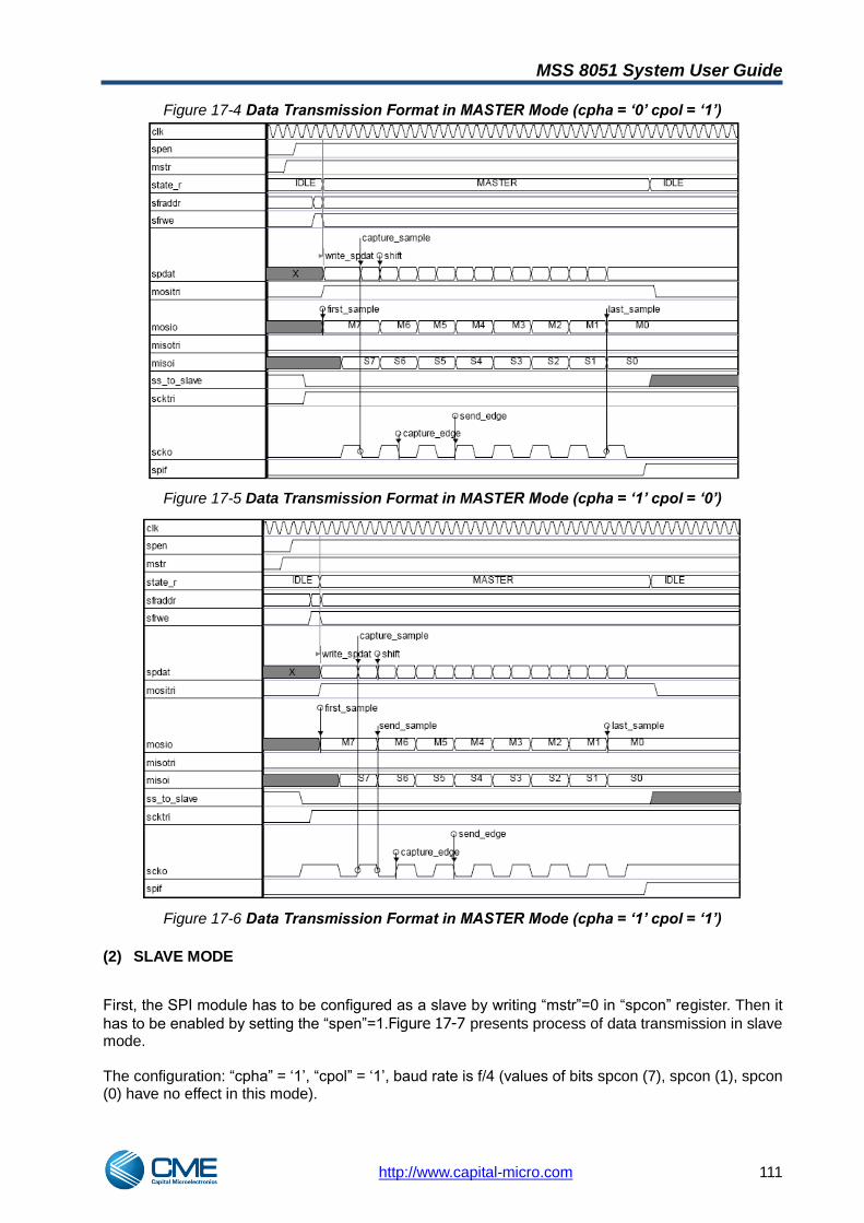
MSS 8051 System User Guide
http://www.capital-micro.com 111
Figure 17-4 Data Transmission Format in MASTER Mode (cpha = „0‟ cpol = „1‟)
Figure 17-5 Data Transmission Format in MASTER Mode (cpha = „1‟ cpol = „0‟)
Figure 17-6 Data Transmission Format in MASTER Mode (cpha = „1‟ cpol = „1‟)
(2) SLAVE MODE
First, the SPI module has to be configured as a slave by writing ―mstr‖=0 in ―spcon‖ register. Then it
has to be enabled by setting the ―spen‖=1.Figure 17-7 presents process of data transmission in slave mode. The configuration: ―cpha‖ = ‗1‘, ―cpol‖ = ‗1‘, baud rate is f/4 (values of bits spcon (7), spcon (1), spcon (0) have no effect in this mode).
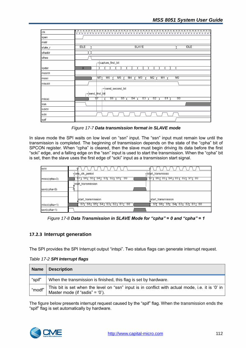
MSS 8051 System User Guide
http://www.capital-micro.com 112
Figure 17-7 Data transmission format in SLAVE mode In slave mode the SPI waits on low level on ―ssn‖ input. The ―ssn‖ input must remain low until the transmission is completed. The beginning of transmission depends on the state of the ―cpha‖ bit of SPCON register. When ―cpha‖ is cleared, then the slave must begin driving its data before the first ―scki‖ edge, and a falling edge on the ―ssn‖ input is used to start the transmission. When the ―cpha‖ bit is set, then the slave uses the first edge of ―scki‖ input as a transmission start signal.
Figure 17-8 Data Transmission in SLAVE Mode for “cpha” = 0 and “cpha” = 1
17.2.3 Interrupt generation
The SPI provides the SPI Interrupt output ―intspi‖. Two status flags can generate interrupt request. Table 17-2 SPI Interrupt flags
Name Description
―spif‖ When the transmission is finished, this flag is set by hardware.
―modf‖ This bit is set when the level on ―ssn‖ input is in conflict with actual mode, i.e. it is ‗0‘ in Master mode (if ―ssdis‖ = ‗0‘).
The figure below presents interrupt request caused by the ―spif‖ flag. When the transmission ends the ―spif‖ flag is set automatically by hardware.
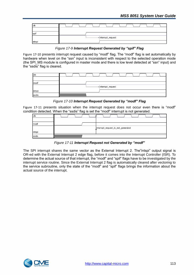
MSS 8051 System User Guide
http://www.capital-micro.com 113
Figure 17-9 Interrupt Request Generated by “spif” Flag
Figure 17-10 presents interrupt request caused by ―modf‖ flag. The ―modf‖ flag is set automatically by
hardware when level on the ―ssn‖ input is inconsistent with respect to the selected operation mode (the SPI_MS module is configured in master mode and there is low level detected at ―ssn‖ input) and the ―ssdis‖ flag is cleared.
Figure 17-10 Interrupt Request Generated by “modf” Flag
Figure 17-11 presents situation when the interrupt request does not occur even there is ―modf‖
condition detected. When the ―ssdis‖ flag is set the ―modf‖ interrupt is not generated.
Figure 17-11 Interrupt Request not Generated by “modf” The SPI interrupt shares the same vector as the External Interrupt 2. The‖intspi‖ output signal is OR-ed with the External Interrupt 2 edge flag, before it comes into the Interrupt Controller (ISR). To determine the actual source of that interrupt, the ―modf‖ and ―spif‖ flags have to be investigated by the interrupt service routine. Since the External Interrupt 2 flag is automatically cleared after vectoring to the service subroutine, only the state of the ―modf‖ and ―spif‖ flags brings the information about the actual source of the interrupt.
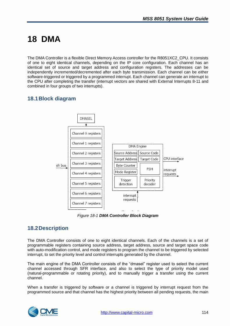
MSS 8051 System User Guide
http://www.capital-micro.com 114
18 DMA
The DMA Controller is a flexible Direct Memory Access controller for the R8051XC2_CPU. It consists of one to eight identical channels, depending on the IP core configuration. Each channel has an identical set of source and target address and configuration registers. The addresses can be independently incremented/decremented after each byte transmission. Each channel can be either software-triggered or triggered by a programmed interrupt. Each channel can generate an interrupt to the CPU after completing the transfer (interrupt vectors are shared with External Interrupts 8-11 and combined in four groups of two interrupts).
18.1 Block diagram
Figure 18-1 DMA Controller Block Diagram
18.2 Description
The DMA Controller consists of one to eight identical channels. Each of the channels is a set of programmable registers containing source address, target address, source and target space code with auto-modification control, and mode registers to program the channel to be triggered by selected interrupt, to set the priority level and control interrupts generated by the channel. The main engine of the DMA Controller consists of the ―dmasel‖ register used to select the current channel accessed through SFR interface, and also to select the type of priority model used (natural-programmable or rotating priority), and to manually trigger a transfer using the current channel. When a transfer is triggered by software or a channel is triggered by interrupt request from the programmed source and that channel has the highest priority between all pending requests, the main

MSS 8051 System User Guide
http://www.capital-micro.com 115
engine of the DMA controller copies all the registers from selected channel to its own working registers, which are used directly to control the CPU. At first, the ―dmareq‖ signal is activated to stop the CPU from instruction execution and to enter the ―hold‖ mode. The CPU acknowledges with the ―dmaack‖ signal, which the DMA controller receives as a permission to start the transfer. The ―dmasrcaddr‖, ―dmasrccode‖, ―dmataraddr‖ and―dmatarcode‖ are driven simultaneously with the proper values of address and space codes used for source and target respectively. The ―dmastart‖ is activated for a single clock cycle to trigger the CPU to perform a transfer from ―source‖ to ―target‖ (one byte only). When completed, the CPU acknowledges the end of transfer using the ―dmaend‖ signal, activated for one clock cycle. Between ―dmastart‖ and ―dmaend‖ the DMA controller cannot change the values of any address or space code bus. After receiving the ―dmaend‖ signal, the DMA controller modifies the Byte Counter, Source Address and Target Address registers, depending on configuration stored previously in the DMA Mode Registers. Once the Byte Counter reaches zero, the DMA controller acknowledges the selected interrupt source which has triggered the transfer, and deasserts the ―dmareq‖ signal to allow the CPU to resume program execution. There are two exceptional situations that can take place during the transfer. One is when there is an external ―hold‖ request to the CPU, which has priority over the DMA controller. When the ―hold‖ input to the CPU is asserted, the CPU finishes current byte transfer triggered by the DMA, and deasserts the ―dmaack‖ together with asserting the ―holda‖, to give the bus access to the external device and to take away from DMA controller. During that, the DMA controller waits until the ―dmaack‖ is active again. The DMA can modify any of the output signals only when there is the ―dmaack‖ active. Also the DMA controller must not sample any of the signals from the CPU (―dmaack‖, ―dmaend‖) when there is a waitstate (―waitstaten‖=0). The other situation is when there is a channel with higher priority triggered during the transfer of another channel. In such case, the lower-priority channel transfer is interrupted and the contents of all registers of the new channel are copied to the internal working registers of the DMA engine. Whenever a transfer gets interrupted by another transfer with higher priority, the contents of working source and target address registers as long as the working byte counter are copied back to the registers of the channel which was triggered previously, to allow to get back to the interrupted transfer after finishing the new one. The same happens at the end of a transfer, when the source and target address are updated from the working registers. The byte counter is written with zero.
Table 18-1 DMA Priority Structure
Natural Priority
Rotating Priority
Each transfer changes priority structure
Highest Lowest
Channel0 Channel1 Channel2 Channel3 Channel4 Channel5 Channel6 Channel7
Channel0 Channel1 Channel2 Channel3 Channel4 Channel5 Channel6 Channel7
Channel1 Channel2 Channel3 Channel4 Channel5 Channel6 Channel7 Channel0
Channel2 Channel3 Channel4 Channel5 Channel6 Channel7 Channel0 Channel1
Channel3 Channel4 Channel5 Channel6 Channel7 Channel0 Channel1 Channel2
….. Channel7 Channel0 Channel1 Channel2 Channel3 Channel4 Channel5 Channel6

MSS 8051 System User Guide
http://www.capital-micro.com 116
Figure 18-2 CPU – DMA Operation with no Stretch
Figure 18-3 CPU – HOLD During DMA Operation

MSS 8051 System User Guide
http://www.capital-micro.com 117
19 RTC
The Real Time Clock realizes a real time count with a resolution of 1/256th second. It allows the user to read seconds, minutes, hours, day of the week and the date. The date is represented by a 16-bit number, which value is interpreted by the user software. The RTC enables a count of 179 years. The RTC features an alarm function which may be used to generate interrupts at a given time during a day or periodically. These interrupts may be used to resume operation from the IDLE/STOP mode at a given time.
19.1 Block diagram
rtcx Divider
/16
Seconds
6bits
Minutes
6bits
hours
5bits
Weeks
3bits
Days
16bits
Alarm Match Comparator
Second
Alarm reg
Minute
Alarm reg
Hours
Alarm reg
rtc control
register
1hz
Serial interface with mcu
Figure 19-1 RTC Block Diagram
19.2 Description
19.2.1 RTC Internal Special Function Registers
The R8051XC2 uses the three RTCSEL, RTCCMD and RTCDATA SFR to operate the Real Time Clock through 10 RTC internal special function registers: six that keep time count (rtcs, rtcm, rtch, rtcw, rtcd1, rtcd0) and three that control the alarm time (rtas, rtam, rtah) and one that controls the RTC operations .
(1) RTCC - Real Time Clock Control register
RTCC: Offset Address – 00h Reset value – 00h Table 19-1 RTCC Register
Bit Symbol Description Type
rtcc.7 sce Second Compare Enable When set to 1 enables a match between rtcs and rtas registers when evaluating an alarm condition; when set to 0 disables this match and thus an interrupt per
R/W

MSS 8051 System User Guide
http://www.capital-micro.com 118
Bit Symbol Description Type
second is generated as long as other registers match. This bit is reset only by the ―rtcreset‖.
rtcc.6 mce Minute Compare Enable When set to 1 enables a match between rtcm and rtam registers when evaluating an alarm condition; when set to 0 disables this match and thus one interrupt per minute is generated as long as other registers match. This bit is reset only by the ―rtcreset‖.
R/W
rtcc.5 hce Hour Compare Enable When set to 1 enables a match between rtch and rtah registers when evaluating an alarm condition; when set to 0 disables this match and thus one interrupt per hour is generated as long as other registers match. This bit is reset only by the ―rtcreset‖.
R/W
rtcc.4 rtcc.3 rtcc.2
Not used, read as 0 R/W R/W R/W
rtcc.1 rtcif Real Time Clock Interrupt Flag The bit is set when a match has been detected between all enabled alarm registers and their corresponding clock registers. It must be cleared by software following an interrupt. Clearing all compare enable bits (rtcc.7-4) will also clear this bit. RTC interrupts cannot be generated by setting this bit (as it cannot be set in software). This bit is reset only by the ―rtcreset‖.
R/W
rtcc.0 rtce Real Time Clock Enable This bit enables (or disables) RTC operation as it works as an enable signal for all registers triggered by the clock signal (rtcx) from the real time clock oscillator. This bit is reset only by the ―rtcreset‖.
R/W
(2) RTCS - Real Time Clock Second Register
RTCs: Offset Address – 01h Reset value – 00h Table 19-2 RTCS Register
Bit Symbol Description Type
rtcs.7 rtcs.6
- Not used, read as 0 R
rtcs.5~rtcs.0 These bits represent the second value of the RTC. The register counts from 0H to 3BH (59 dec). The user is responsible for writing only the values in this range to the rtcs register.
R/W
(3) RTCM - Real Time Clock Minute Register
RTCM: Offset Address – 02h Reset value – 00h

MSS 8051 System User Guide
http://www.capital-micro.com 119
Table 19-3 RTCM Register
(4) RTCH - Real Time Clock Hour Register
RTCH: Offset Address – 03h Reset value – 00h Table 19-4 RTCH Register
Bit Symbol Description Type
rtch.7 rtch.6 rtch.5 - Not used, read as 0 R/W
rtch.4~rtch.0 - These bits represent the hour value of the RTC. This register counts from 0H to 17H (23 dec).
R/W
(5) RTCW-Real Time Clock Week Register
RTCW: Offset Address – 04h Reset value – 00h Table 19-5 RTCW Register
Bit Symbol Description Type
rtch.7~ rtch.3 Not used, read as 0 R/W
rtch.2~rtch.0 - These bits represent the week value of the RTC. This register counts from 1H to 7H, 1 for Sun, 7 for Sat.
R/W
(6) RTCD0-Real Time Clock Day Register 0
RTCD0: Offset Address – 06h Reset value – 00h Table 19-6 RTCD0 Register
Bit Symbol Description Type
rtcm.7 rtcm.6
- Not used, read as 0 R
rtcm.5~ rtcm.0 - These bits represent the minute value of the RTC. The register counts from 0H to 3BH (59 dec). The user is responsible for writing only the values in this range to the rtcm register.
R/W
MSS 8051 System User Guide
http://www.capital-micro.com 120
(7) RTCD1-Real Time Clock Day Register 1
RTCD1: Offset Address – 06h Reset value – 00h Table 19-7 RTCM Register
(8) RTAS - Real Time Alarm Second Register
RTCM: Offset Address – 08h Reset value – 00h Table 19-8 RTCAS Register
Bit Symbol Description Type
rtas.7 rtas.6
- Not used, read as 0 R
rtas.5~rtas.0 - These bits represent a second value of alarm that will be compared against corresponding bits of the Real Time Clock Second Register (rtcs.5-0) provided that sce bit (rtcc.6) is set. This register is reset only by the ―rtcreset‖.
R/W
(9) RTAM - Real Time Alarm Minute Register
RTAM: Offset Address – 09h Reset value – 00h
Bit Symbol Description Type
rtcd1.7 ~rtcd1.0
- The rtcd0 register bits represents the lest significant part of the 16-bit current day count. The day count should be seen as a value set by the user relative to a user specified calendar date. It is up to user software to interpret its contents in terms of an absolute date. No alarm register is compared against these bits.
R/W
Bit Symbol Description Type
rtcd1.7~rtcd1.0 - The rtcd1 register bits represents the most significant part of the 16-bit current day count. The day count should be seen as a value set by the user relative to a user specified calendar date. It is up to user software to interpret its contents in terms of an absolute date. No alarm register is compared against these bits.
R/W

MSS 8051 System User Guide
http://www.capital-micro.com 121
Table 19-9 RTAM Register
Bit Symbol Description Type
rtam.7 rtam.6
- Not used, read as 0 R
rtam.5 ~rtam.0 - These bits represent a minute value of alarm that will be compared against corresponding bits of the Real Time Clock Alarm Register (rtcm.5-0) provided that mce bit (rtcc.5) is set. This register is reset only by the ―rtcreset‖.
R/W
(10) RTAH - Real Time Alarm Hour Register
RTAH: Offset Address – 0Ah Reset value – 00h
Table 19-10 RTAH Register
19.2.2 Operating
(1) Starting and Stopping the RTC
Starting and stopping the RTC is controlled with rtce bit (rtcc.0). When the bit is set all the registers triggered with the RTC clock (rtcx) are enabled and the RTC counters are clocked. When this bit is cleared the state of the registers freezes. The value of the clock registers will be preserved along with all control and alarm settings.
(2) Setting and Reading the RTC Registers
Access to the RTC registers (rtcw, rtcs, rtcm, rtch, rtcd0, rtcd1) is controlled via the three SFR of RTCCMD, RTCSEL and RTCDATA For example: Write 1h to RTCC //write RTCC value 0x1 to RTCDATA RTCDATA = 0x1 //write 0x8 to RTCSEL to select the RTCC and set write operation RTCSEL = 0x8 //write RTCCMD value 0x80 to write 0x1 value to RTCC RTCCMD = 0x80 For example: Read RTCC //write 0x0 to RTCSEL to select the RTCC and set read operation RTCSEL = 0x0 //write RTCCMD value 0x80 to trigger the internal read from RTCC
Bit Symbol Description Type
rtah.7 rtah.6 rtah.5
- Not used, read as 0 R
rtah.4~rtah.0 - These bits represent an hour value of alarm that will be compared against corresponding bits of the Real Time Clock Hour Register (rtch.4-0) provided that hce bit (rtcc.4) is set. This register is reset only by the ―rtcreset‖.
R/W

MSS 8051 System User Guide
http://www.capital-micro.com 122
RTCCMD = 0x80 //Read RTCC value to P0 P0 = RTCDATA Writing an invalid time (i.e. a value outside the range representing valid second, minute or hour value) to the RTC registers will result in an inaccurate count by RTC.
(1) Using the RTC Alarm
The alarm function is used to generate an interrupt when the RTC value matches a value from the enabled alarm register. When the RTC reaches the selected alarm value, it sets a flag (rtcif). This will cause an interrupt if enabled, even in Stop mode. With interrupt not enabled, it can still wake-up the R8051XC2 from IDLE or STOM mode. The user selects the alarm time by setting the rtas, rtam and rtah registers. There is no specific alarm register bound to the RTC Day count or RTC Day of Week register. Therefore it is up to user software to control the execution of an alarm that is desired only at a specific date. Writing an invalid value (e.g. 61 to rtam or rtah registers) will never cause a match. It is the responsibility of the user to ensure that only valid time values are written to alarm registers. The alarm function is implemented with a comparator that matches the alarm value set by the user against the current RTC value. The user can select a match of one or more of the following registers: rtas, rtam and rtah against their RTC counterparts by setting appropriate compare enable bits (rtcc.7-5). Any RTC register that has a corresponding compare enable bit set to 0 is treated as a match. This allows an alarm to occur once a day at specific point in time (when all compare enable bits are set) or periodically - once per second, once per minute, once per hour within a given period of time (depending on a combination of the compare enable bits that are set). The general procedure for setting the alarm registers to cause an RTC interrupt is as follows:
clear all alarm compare enable bits (rtcc.7-5), write one or more alarm registers (rtas, rtam, rtah), Set the desired alarm compare enable bits (rtcc.7-5)

MSS 8051 System User Guide
http://www.capital-micro.com 123
20 HOLD Interface
The Hold Interface input is sampled at the beginning of a new instruction, at the same time as the instruction word is captured from program memory data bus. If that sample is active, the FSM proceeds to the Hold Mode: it clears the instruction register, suppresses program memory fetch, moves the Program Counter back as if the last fetch did not happen, and acknowledges using the ―holda‖ output. In that state, the ―hold‖ input is sampled at each clock cycle. The interrupt request is not taken into account in Hold Mode. If during the Hold Mode an interrupt occurs then the core activates ―intoccur‖ output. When the ―hold‖ becomes inactive, the FSM resumes program execution by initiating a new instruction pre-fetch and disabling the acknowledge output (―holda‖). When the ―hold‖ input goes active during the Power-Down Mode it proceeds to the Hold Mode and ‗holda‘ output is activated. The state of the Power-Down flags in the ―pcon‖ register remain unchanged. When the ―hold‖ input is disabled, the CPU deactivates ‗holda‘ output and returns to the Power-Down Mode as defined by flags in the ―pcon‖ register. If ―hold‖ goes active in Debug Mode and there is no pending single step operation then ‗debugack‘ output is deactivated, the core enters Hold Mode and ‗holda‘ output is activated. When ‗hold‘ input becomes inactive then ‗holda‘ output is deactivated, the core enters Debug Mode and activates ‗debugack‘ output or executes instructions if ‗debugreq‘ input is inactive. If ―hold‖ goes active in Debug Mode when single-step is executed then step operation is finished, ―debugack‖ stays inactive and ―holda‖ acknowledge output is activated. The core enters Hold Mode. When the ―hold‖ input becomes inactive ―holda‖ output is deactivated, ―debugack‖ goes active and the core enters into Debug Mode.
20.1 CPU- Hold Request Timing
Figure 20-1 CPU- Hold Request Timing
20.2 CPU- Hold Request During Debug Mode
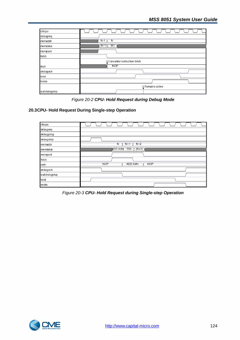
MSS 8051 System User Guide
http://www.capital-micro.com 124
Figure 20-2 CPU- Hold Request during Debug Mode
20.3 CPU- Hold Request During Single-step Operation
Figure 20-3 CPU- Hold Request during Single-step Operation
MSS 8051 System User Guide
http://www.capital-micro.com 125
21 Revision History
Table below shows the revision history for this document.
Date Version Revision
07/2012 1.0 Initial release.
09/2012 CME8051UGE02 Update the styles
03/2013 CME8051UGE03 Update