msw201x-201 - macom · sp2t pin diode switch rev. v1 msw201x-201 11 m/a-com technology solutions...
TRANSCRIPT
SP2T PIN Diode Switch
Rev. V1
MSW201x-201
1 1
M/A-COM Technology Solutions Inc. (MACOM) and its affiliates reserve the right to make changes to the product(s) or information contained herein without notice. Visit www.macom.com for additional data sheets and product information.
For further information and support please visit: https://www.macom.com/support
DS-xxxxxxx
1
Features
Wide Frequency Range: 50 MHz to 4 GHz, in 2 bands
Surface Mount SP2T Switch in Compact Outline: 8 mm L x 5 mm W x 2.5 mm H
Higher Average Power Handling than Plastic Packaged
MMIC Switches: 100 W CW
High RF Peak Power: 500 W
Low Insertion Loss: 0.25 dB
High IIP3: 65 dBm
Operates From Positive Voltage Only: 5 V & 28 V to 125 V
Ultra-Thin Termination Plating to Combat Embrittlement
RoHS* Compliant
Description
The MSW2010-201 (50 MHz - 1 GHz) and MSW2011-201 (400 MHz - 4 GHz) series of surface mount silicon PIN diode SP2T switches can be used for high power transmit/receive (TR) switching or active receiver protection. These switches are manufactured using a proven hybrid manufacturing process incorporating high voltage PIN diodes and passive devices integrated on a ceramic substrate. These low profile, compact, surface mount components offer superior small and large signal performance compared to that of MMIC devices in QFN packages. The SP2T switches are designed in an asymmetrical topology to minimize Tx-Ant loss and maximize Tx-Rx isolation performance. The very low thermal resistance (<10ºC/W ) of the PIN diodes in these devices enables them to reliably handle RF incident power levels of 50 dBm CW and RF peak incident power levels of 53 dBm in cold switching applications at TA = 85ºC. The thick I layers of the PIN diodes, coupled with their long minority carrier lifetime, provides input third order intercept point (IIP3) greater than 60 dBm.
The MSW2010-201 and MSW2011-201 SP2T switches are designed to be used in high average and peak power switch applications, operating from 50 MHz to 4 GHz in two bands, which utilize high volume, surface mount, solder re-flow manufacturing. These products are durable and capable of reliably operating in military, commercial, and industrial environments.
Ordering Information
Part Number Package
MSW2010-201-T tube
MSW2010-201-R 250 or 500 piece reel
MSW2010-201-W Waffle pack
MSW2011-201-T tube
MSW2011-201-R 250 or 500 piece reel
MSW2011-201-W Waffle pack
MSW2010-201-E RF evaluation board
MSW2011-201-E RF evaluation board
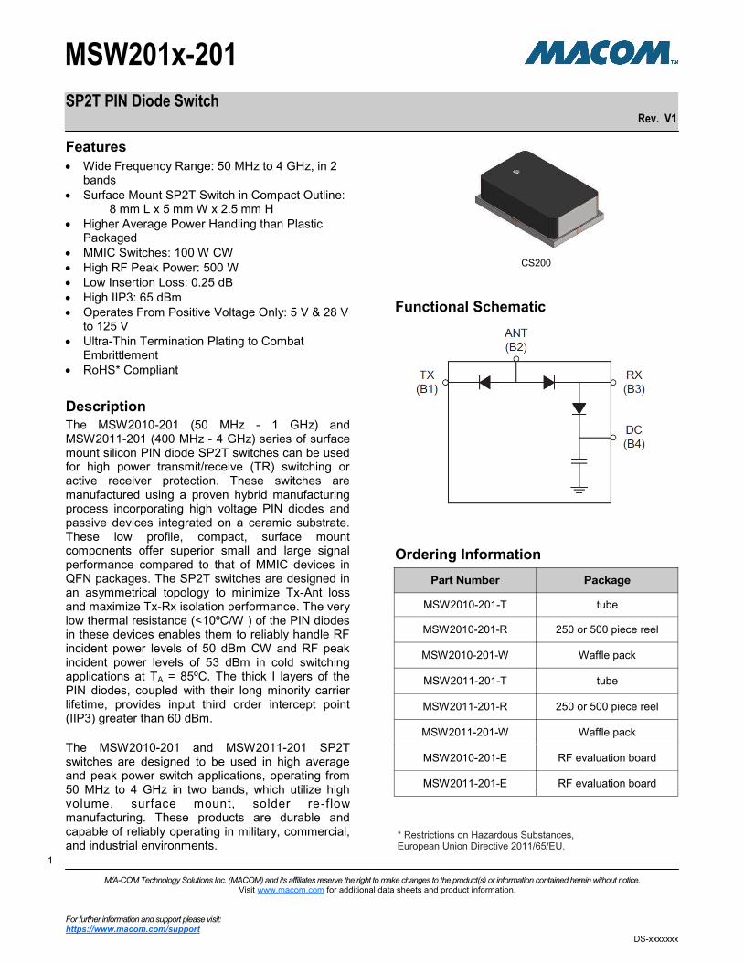
CS200
* Restrictions on Hazardous Substances, European Union Directive 2011/65/EU.
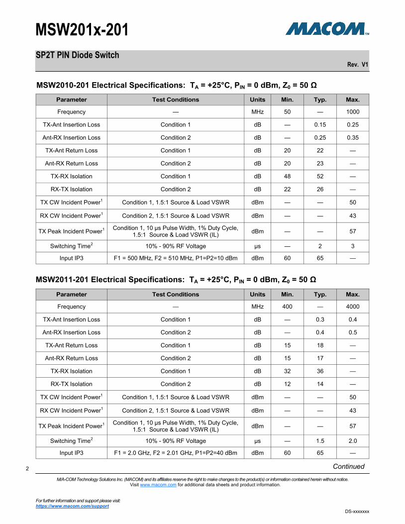
Functional Schematic
SP2T PIN Diode Switch
Rev. V1
MSW201x-201
2 2
M/A-COM Technology Solutions Inc. (MACOM) and its affiliates reserve the right to make changes to the product(s) or information contained herein without notice. Visit www.macom.com for additional data sheets and product information.
For further information and support please visit: https://www.macom.com/support
DS-xxxxxxx
2
MSW2010-201 Electrical Specifications: TA = +25°C, PIN = 0 dBm, Z0 = 50 Ω
Parameter Test Conditions Units Min. Typ. Max.
Frequency — MHz 50 — 1000
TX-Ant Insertion Loss Condition 1 dB — 0.15 0.25
Ant-RX Insertion Loss Condition 2 dB — 0.25 0.35
TX-Ant Return Loss Condition 1 dB 20 22 —
Ant-RX Return Loss Condition 2 dB 20 23 —
TX-RX Isolation Condition 1 dB 48 52 —
RX-TX Isolation Condition 2 dB 22 26 —
TX CW Incident Power1 Condition 1, 1.5:1 Source & Load VSWR dBm — — 50
RX CW Incident Power1 Condition 2, 1.5:1 Source & Load VSWR dBm — — 43
TX Peak Incident Power1 Condition 1, 10 µs Pulse Width, 1% Duty Cycle,
1.5:1 Source & Load VSWR (IL) dBm — — 57
Switching Time2 10% - 90% RF Voltage µs — 2 3
Input IP3 F1 = 500 MHz, F2 = 510 MHz, P1=P2=10 dBm dBm 60 65 —
Continued
MSW2011-201 Electrical Specifications: TA = +25°C, PIN = 0 dBm, Z0 = 50 Ω
Parameter Test Conditions Units Min. Typ. Max.
Frequency — MHz 400 — 4000
TX-Ant Insertion Loss Condition 1 dB — 0.3 0.4
Ant-RX Insertion Loss Condition 2 dB — 0.4 0.5
TX-Ant Return Loss Condition 1 dB 15 18 —
Ant-RX Return Loss Condition 2 dB 15 17 —
TX-RX Isolation Condition 1 dB 32 36 —
RX-TX Isolation Condition 2 dB 12 14 —
TX CW Incident Power1 Condition 1, 1.5:1 Source & Load VSWR dBm — — 50
RX CW Incident Power1 Condition 2, 1.5:1 Source & Load VSWR dBm — — 43
TX Peak Incident Power1 Condition 1, 10 µs Pulse Width, 1% Duty Cycle,
1.5:1 Source & Load VSWR (IL) dBm — — 57
Switching Time2 10% - 90% RF Voltage µs — 1.5 2.0
Input IP3 F1 = 2.0 GHz, F2 = 2.01 GHz, P1=P2=40 dBm dBm 60 65 —
SP2T PIN Diode Switch
Rev. V1
MSW201x-201
3 3
M/A-COM Technology Solutions Inc. (MACOM) and its affiliates reserve the right to make changes to the product(s) or information contained herein without notice. Visit www.macom.com for additional data sheets and product information.
For further information and support please visit: https://www.macom.com/support
DS-xxxxxxx
3
1. PIN diode DC reverse voltage to maintain high resistance in the OFF PIN diode is determined by RF frequency, incident power, and VSWR as well as by the characteristics of the diode. The minimum reverse bias voltage values are provided in this datasheet. The input signal level applied for small signal testing is approximately 0 dBm.
2. Switching time (50% TTL - 10/90% RF Voltage) is a function of the PIN diode driver performance as well as the characteristics of the diode. An RC “current spiking network” is used on the driver output to provide a transient current to rapidly remove stored charge from the PIN diode. Typical component values are: R = 50 to 220 Ω and C = 470 to 1,000 pF. MACOMs MPD2T28125-700 is the recommended PIN diode driver to interface with the MSW2010-201 and MSW2011-201 SP2T switches. Its data sheet is available.
Bias State Conditions:
Transmit State (TX - ANT in low insertion loss state): a. B1: -100 mA b. B2: +100 mA c. B3: -25 mA, +28 V d. B4: +25 mA
Small Signal Receive State (ANT - RX in low insertion loss state): a. B1: +28 V b. B2: +100 mA c. B3: -100 mA, 0 V d. B4: +28 V
Truth Table
RF Bias Network Component Values
Part # Frequency (MHz) Inductors DC Blocking Capacitors RF Bypass Capacitors
MSW2010-201 50 - 1000 4.7 µH 0.1 µF 0.1 µF
MSW2011-201 400 - 4000 43 nH 47 pF 270 pF
Evaluation Board Truth Table
Port J0 - J1
Port J0 - J2
Bias: B1 Bias: B2 Bias: B3 Bias: B4
Low Loss Isolation -100 mA +100 mA +25 mA @ +28 V -25 mA
Isolation Low Loss +28 V +100 mA -100 mA +28 V
Port J0 - J1
Ant Bias (P1-pin 3) TX Bias (P1-pin 1) RX Bias (P1-pin 7) DC Bias (P1-pin 5)
TX-ANT Low Loss & TX-RX Isolation
+5 V @ +100 mA 0 V @ -100 mA +28 V @ +25 mA 0 V @ -25 mA
ANT-RX Low Loss & RX-TX Isolation
+5 V @ +100 mA +28 V @ 0 mA 0 V @ +100 mA +28 V @ 0 mA

SP2T PIN Diode Switch
Rev. V1
MSW201x-201
4 4
M/A-COM Technology Solutions Inc. (MACOM) and its affiliates reserve the right to make changes to the product(s) or information contained herein without notice. Visit www.macom.com for additional data sheets and product information.
For further information and support please visit: https://www.macom.com/support
DS-xxxxxxx
4
Minimum Reverse Bias Voltage3: PINC = 125 W CW, Z0 = 50 Ω with 1.5:1 VSWR
Part # 20 MHz 100 MHz 200 MHz 400 MHz 1 GHz 4 GHz
MSW2010-201 120 V 110 V 85 V 55 V 28 V N/A
MSW2011-201 N/A N/A 110 V 85 V 55 V 28 V
3. N/A denotes the switch is not recommended for that frequency band.
Where: |VDC| = magnitude of the minimum DC reverse bias voltage |VRF| = magnitude of the peak RF voltage (including the effects of the VSWR) FMHz = lowest RF signal frequency expressed in MHz D = duty factor of the RF signal WMILS = thickness of the diode I layer, expressed in mils (thousands of an inch) R. Caverly and G. Hiller, ―Establishing the Minimum Reverse Bias for a PIN Diode in a High Power Switch, IEEE Transac-tions on Microwave Theory and Techniques, Vol.38, No.12, December 1990
The minimum reverse bias voltage required to maintain a PIN diode out of conduction in the presence of a large RF signal is given by:
SP2T PIN Diode Switch
Rev. V1
MSW201x-201
5 5
M/A-COM Technology Solutions Inc. (MACOM) and its affiliates reserve the right to make changes to the product(s) or information contained herein without notice. Visit www.macom.com for additional data sheets and product information.
For further information and support please visit: https://www.macom.com/support
DS-xxxxxxx
5
Absolute Maximum Ratings
Parameter Conditions Absolute Maximum
Forward Current Ant, TX or RX Port
DC Port 250 mA 150 mA
Reverse Voltage TX or RX Port
DC Port 125 V 125 V
Forward Diode Voltage IF = 250 mA 1.2 V
CW Incident Power Handling4 TX or Ant Port
Source & Load VSWR = 1.5:1, TC = 85°C, cold switching
50 dBm
CW Incident Power Handling4 RX or Ant Port
Source & Load VSWR = 1.5:1, TC = 85°C, cold switching
43 dBm
Peak Incident Power Handling4 RX or Ant Port
Source & Load VSWR = 1.5:1, TC = 85°C, cold switching, Pulse Width = 10 µs, Duty Cycle = 1%
57 dBm
Total Dissipated RF & DC Power4 TC = 85°C, cold switching 8 W
Junction Temperature — +175°C
Operating Temperature — -65°C to +125°C
Storage Temperature — -65°C to +150°C
Assembly Temperature t = 10 s +260°C
Handling Procedures
Please observe the following precautions to avoid damage:
Static Sensitivity
These electronic devices are sensitive to electrostatic discharge (ESD) and can be damaged by static electricity. Proper ESD control techniques should be used when handling these Class 1C (HBM) devices. The moisture sensitivity level (MSL) rating for this part is MSL 1.
Environmental Capabilities
The MSW204x-204 diode is capable of meeting the environmental requirements of MIL-STD-202 and MIL-STD-750.
4. Backside RF and DC grounding area of device must be completely solder attached to the RF circuit board vias for proper electrical and thermal circuit grounding.

SP2T PIN Diode Switch
Rev. V1
MSW201x-201
6 6
M/A-COM Technology Solutions Inc. (MACOM) and its affiliates reserve the right to make changes to the product(s) or information contained herein without notice. Visit www.macom.com for additional data sheets and product information.
For further information and support please visit: https://www.macom.com/support
DS-xxxxxxx
6
Typical Performance Curves
Isolation
Insertion Loss
MSW2010-201 MSW2011-201
Isolation
Insertion Loss
SP2T PIN Diode Switch
Rev. V1
MSW201x-201
7 7
M/A-COM Technology Solutions Inc. (MACOM) and its affiliates reserve the right to make changes to the product(s) or information contained herein without notice. Visit www.macom.com for additional data sheets and product information.
For further information and support please visit: https://www.macom.com/support
DS-xxxxxxx
7
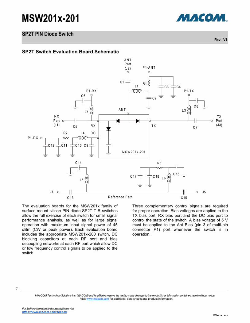
SP2T Switch Evaluation Board Schematic
The evaluation boards for the MSW201x family of surface mount silicon PIN diode SP2T T-R switches allow the full exercise of each switch for small signal performance analysis, as well as for large signal operation with maximum input signal power of 45 dBm (CW or peak power). Each evaluation board includes the appropriate MSW201x-200 switch, DC blocking capacitors at each RF port and bias decoupling networks at each RF port which allow DC or low frequency control signals to be applied to the switch.
Three complementary control signals are required for proper operation. Bias voltages are applied to the TX bias port, RX bias port and the DC bias port to control the state of the switch. A bias voltage of 5 V must be applied to the Ant Bias (pin 3 of multi-pin connector P1) port whenever the switch is in operation.

SP2T PIN Diode Switch
Rev. V1
MSW201x-201
8 8
M/A-COM Technology Solutions Inc. (MACOM) and its affiliates reserve the right to make changes to the product(s) or information contained herein without notice. Visit www.macom.com for additional data sheets and product information.
For further information and support please visit: https://www.macom.com/support
DS-xxxxxxx
8
Transmit State
In the TX state, the series PIN diode between the ANT and TX ports is forward biased by applying 0 V to the TX bias input port (pin 1 of multi-pin connector P1). The magnitude of the resultant bias current through the diode is primarily determined by the voltage applied to the ANT bias port (pin 3 of J1), the magnitude of the forward voltage across the PIN diode and the resistance of R1. This current is nominally 100 mA. At the same time, the PIN diode connected between RX and DC ports is also forward biased by applying a higher bias voltage, nominally 28 V, to the RX bias port (pin 7 of P1) and 0 V to the DC bias port (pin 5 of P1). Under this condition, the PIN diode connected between the ANT and RX port is reverse biased and the PIN diode connected between the RX and DC ports is forward biased. The magnitude of the bias current through this diode is primarily determined by the voltage applied to the RX bias port, the magnitude of the forward voltage across the PIN diode and the resistance of R2. This current is nominally 25 mA. The RX series PIN diode, which is connected between the ANT and RX ports, must be reverse biased during the transmit state. The reverse bias voltage must be sufficiently large to maintain the diode in its non-conducting, high impedance state when large RF signal voltage may be present in the ANT-to-TX path. The reverse voltage across this diode is the arithmetic difference of the bias voltage applied to the RX bias port and the DC forward voltage of the forward-biased transmit series PIN diode. The minimum voltage required to maintain the series diode on the RX side of the switch out of conduction is a function of the magnitude of the RF voltage present, the standing wave present at the RX series diode’s anode, the frequency of the RF signal and the characteristics of the RX series diode, among other factors. Minimum control voltages for several signal frequencies are shown in the table “Minimum Reverse Bias Voltage”, assuming the input power to the RX or ANT port to be 100 W CW and the VSWR on the ANT-TX path to be 1.5:1. It is important to note that the evaluation board, as supplied from the factory, is not capable of handling RF input signals larger than 45 dBm. If performance of the switch under larger input signals is to be evaluated, an adequate heat sink must be properly attached to the
evaluation board, and several of the passive components on the board must be changed in order to safely handle the dissipated power as well as the high bias voltage necessary for proper performance. Contact the factory for recommended components and heat sink.
Receive State
In the RX state, the series PIN diode between the ANT and RX ports is forward biased by applying 0 V to the RX bias input port (pin 7 of multi-pin connector P1). The magnitude of the resultant bias current through the diode is primarily determined by the voltage applied to the ANT bias port (pin 3 of P1), the magnitude of the forward voltage across the PIN diode and the resistance of R1. This current is nominally 100 mA. At the same time, the PIN diode connected between RX and DC ports is reverse biased by applying a high bias voltage, nominally 28 V, to the DC bias port (pin 5 of P1). A high voltage, nominally 28 V, is also applied to the TX bias port (pin 1 of P1). Under this condition, the PIN diode connected between the ANT and TX port is reverse biased thus isolating the TX RF port from the RX signal path. The reverse voltage across this diode is the arithmetic difference of the bias voltage applied to the TX bias port and the DC forward voltage of the forward-biased receive series PIN diode. The minimum voltage required to maintain the series diode on the TX side of the switch out of conduction is a function of the magnitude of the RF voltage present, the standing wave present at the RX series diode’s anode, the frequency of the RF signal and the characteristics of the TX series diode, among other factors. For typical receive-level signals, this diode is held out of conduction with a relatively small reverse bias voltage. The values of the reactive components which comprise the bias decoupling networks as well as the signal path DC blocking are shown in the table RF Bias Network Component Values.
Reference Path
A reference path is provided on the evaluation board, complete with bias decoupling networks, so that the magnitude of the insertion loss of the micro-strip transmission lines connected to the switch and the associated bias decoupling components can be measured and removed from the measured performance of the switch.

SP2T PIN Diode Switch
Rev. V1
MSW201x-201
9 9
M/A-COM Technology Solutions Inc. (MACOM) and its affiliates reserve the right to make changes to the product(s) or information contained herein without notice. Visit www.macom.com for additional data sheets and product information.
For further information and support please visit: https://www.macom.com/support
DS-xxxxxxx
9
SP2T Switch Evaluation Board Layout Evaluation Board Parts List
MSW2010-201 Band 1
Part Value Case Style
C1, C2, C5 - C10, C13 - C15
0.1 µF 0603
5C3, C4, C11, C12, C17, C18
0.1 µF 0603
L1 - L6 47 µH 1008
R1, R3 39 Ω 2512
R2 1200 Ω 2512
MSW2011-201 Band 2
Part Value Case Style
C1, C5, C7, C13, C15 47 pF 0603
C2, C6, C8, C9, C10, C14, C16
220 pF 0603
C3, C4, C11, C12, C17, C18
1000 pF 0603
L1 - L7 43 nH 0603
R1, R3 39 Ω 2512
R2, R4 1200 Ω 2512
7. Second bypass capacitor is optional.

SP2T PIN Diode Switch
Rev. V1
MSW201x-201
10 10
M/A-COM Technology Solutions Inc. (MACOM) and its affiliates reserve the right to make changes to the product(s) or information contained herein without notice. Visit www.macom.com for additional data sheets and product information.
For further information and support please visit: https://www.macom.com/support
DS-xxxxxxx
10
Assembly Instructions
SP2T PIN Diodes may be placed onto circuit boards with pick and place manufacturing equipment from tape and reel. The devices are attached to the circuit using conventional solder re-flow or wave soldering procedures with RoHS type or Sn 60 / Pb 40 type solders.
SP2T PIN Diode Switch
Rev. V1
MSW201x-201
11 11
M/A-COM Technology Solutions Inc. (MACOM) and its affiliates reserve the right to make changes to the product(s) or information contained herein without notice. Visit www.macom.com for additional data sheets and product information.
For further information and support please visit: https://www.macom.com/support
DS-xxxxxxx
11
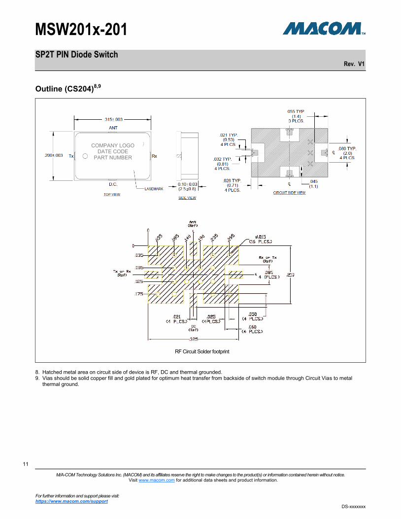
Outline (CS204)8,9
COMPANY LOGO DATE CODE
PART NUMBER
8. Hatched metal area on circuit side of device is RF, DC and thermal grounded. 9. Vias should be solid copper fill and gold plated for optimum heat transfer from backside of switch module through Circuit Vias to metal
thermal ground.
RF Circuit Solder footprint
SP2T PIN Diode Switch
Rev. V1
MSW201x-201
12 12
M/A-COM Technology Solutions Inc. (MACOM) and its affiliates reserve the right to make changes to the product(s) or information contained herein without notice. Visit www.macom.com for additional data sheets and product information.
For further information and support please visit: https://www.macom.com/support
DS-xxxxxxx
12
M/A-COM Technology Solutions Inc. All rights reserved. Information in this document is provided in connection with M/A-COM Technology Solutions Inc ("MACOM")products. These materials are provided by MACOM as a service to its customers and may be used for informational purposes only. Except as provided in MACOM's Terms and Conditions of Sale for such products or in any separate agreement related to this document, MACOM assumes no liability whatsoever. MACOM assumes no responsibility for errors or omissions in these materials. MACOM may make changes to specifications and product descriptions at any time, without notice. MACOM makes no commitment to update the information and shall have no responsibility whatsoever for conflicts or incompatibilities arising from future changes to its specifications and product descriptions. No license, express or implied, by estoppels or otherwise, to any intellectual property rights is granted by this document. THESE MATERIALS ARE PROVIDED "AS IS" WITHOUT WARRANTY OF ANY KIND, EITHER EXPRESS OR IMPLIED, RELATING TO SALE AND/OR USE OF MACOM PRODUCTS INCLUDING LIABILITY OR WARRANTIES RELATING TO FITNESS FOR A PARTICULAR PURPOSE, CONSEQUENTIAL OR INCIDENTAL DAMAGES, MERCHANTABILITY, OR INFRINGEMENT OF ANY PATENT, COPYRIGHT OR OTHER INTELLECTUAL PROPERTY RIGHT. MACOM FURTHER DOES NOT WARRANT THE ACCURACY OR COMPLETENESS OF THE INFORMATION, TEXT, GRAPHICS OR OTHER ITEMS CONTAINED WITHIN THESE MATERIALS. MACOM SHALL NOT BE LIABLE FOR ANY SPECIAL, INDIRECT, INCIDENTAL, OR CONSEQUENTIAL DAMAGES, INCLUDING WITHOUT LIMITATION, LOST REVENUES OR LOST PROFITS, WHICH MAY RESULT FROM THE USE OF THESE MATERIALS. MACOM products are not intended for use in medical, lifesaving or life sustaining applications. MACOM customers using or selling MACOM products for use in such applications do so at their own risk and agree to fully indemnify MACOM for any damages resulting from such improper use or sale.