mtrx1701 soldering labweb.aeromech.usyd.edu.au/mtrxlab/soldering/cap meter kit...on a four digit...
TRANSCRIPT

1
MTRX1701 Soldering Lab
You will complete this soldering exercise as part of the workshop technology component of MTRX1701. Even if you have not previously soldered, with a little care you will be able to assemble a capacitance meter from a kit of parts. The assembled capacitance meter is yours to keep and use.
A single three‐hour lab will not give you enough practice to become proficient at soldering; that takes continual practice. Instead, the objective of the lab is to teach you the correct way to solder and to instil good practice in assembling and soldering electronic components.
0. Safety
You will want to get started, but first consider your safety. This lab uses tools and material that are potentially hazardous. The risks involved in the Soldering Lab have formally been evaluated in accordance with University policy and NSW law. The results of this evaluation are presented as a Project Risk Analysis (PRA) and Safe Operating Procedure (SOP) that are linked from the MTRX1701 Soldering Lab Website. Materials safety data sheets (MSDS) are also linked. This section summarises the risks and required controls.
Soldering iron: Risk: burns. Controls: contain long and loose hair; wear approved safety glasses, to be provided by students.
Solder containing Multicore resin flux 309. Risks: Fumes emitted during soldering may irritate the eyes and skin and may produce an allergic reaction; fumes will irritate the nose, throat and lungs; prolonged or repeated exposure to flux fumes may result in sensitisation. Controls: avoid breathing soldering fumes; air conditioning must be operating; nitrile gloves provided by the University may be worn. Comment: exposure to lead during soldering is not a hazard unless there is a considerable surface area of molten lead, such as occurs in industrial wave soldering.
Isopropanol: Used for de‐fluxing. Risks: Highly flammable; irritating to the eyes; vapours may cause drowsiness and dizziness; may cause lung damage if swallowed. Controls: Keep away from sources of ignition; keep container closed when not in use; wear approved safety glasses (student to provide) and nitrile gloves (University to provide); air conditioning must be operating.
Chemtools Flux Pen: May be required for adding extra flux. This flux is mostly isopropanol with a small percentage of naphtha (petroleum) heavy alkylate. The risks and controls are identical to those for solder and isopropanol.
General: Do not eat or drink when soldering. Wash hands with soap and water before eating or drinking and at the end of the lab.
1. About the Capacitance Meter Kit
This kit allows you to assemble your own capacitance meter that is capable of measuring the values of capacitors between 1 pF (p = pico, or 10‐12) and 500 μF (μ = micro, or 10‐6) with an accuracy between 1% and 2%.
The meter works by using a (pre‐programmed) microcontroller to measure the time taken to charge the unknown capacitor. The charging time is directly proportional to the capacitance. Charging and discharging of the unknown capacitance is controlled by making associated microcontroller ports high, low or high‐impedance (effectively disconnected). The meter outputs the measured capacitance on a four digit 7‐segment LED (light emitting diode) display and as TTL‐level ASCII text through a serial port. An 8‐16 VDC power supply is required, but not included. TTL is transistor‐transistor logic, using (nominally) 0V and +5V to represent logic 0 and logic 1.
2
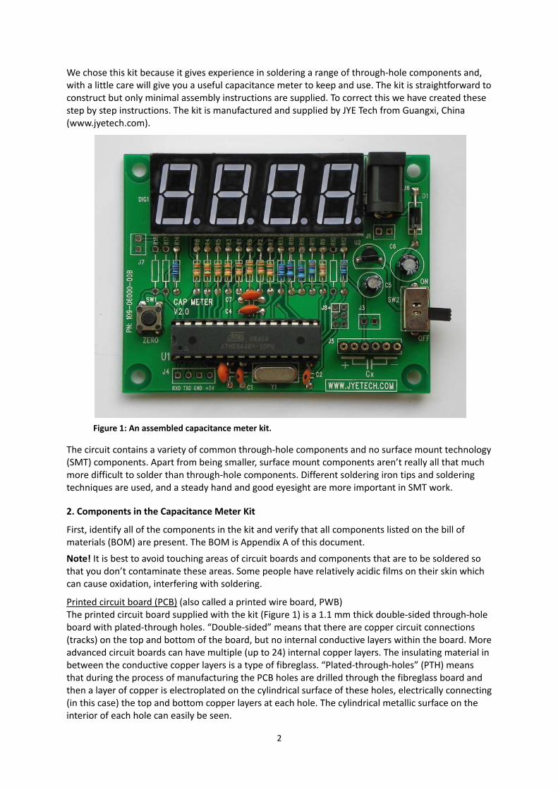
We chose this kit because it gives experience in soldering a range of through‐hole components and, with a little care will give you a useful capacitance meter to keep and use. The kit is straightforward to construct but only minimal assembly instructions are supplied. To correct this we have created these step by step instructions. The kit is manufactured and supplied by JYE Tech from Guangxi, China (www.jyetech.com).
Figure 1: An assembled capacitance meter kit.
The circuit contains a variety of common through‐hole components and no surface mount technology (SMT) components. Apart from being smaller, surface mount components aren’t really all that much more difficult to solder than through‐hole components. Different soldering iron tips and soldering techniques are used, and a steady hand and good eyesight are more important in SMT work.
2. Components in the Capacitance Meter Kit
First, identify all of the components in the kit and verify that all components listed on the bill of materials (BOM) are present. The BOM is Appendix A of this document.
Note! It is best to avoid touching areas of circuit boards and components that are to be soldered so that you don’t contaminate these areas. Some people have relatively acidic films on their skin which can cause oxidation, interfering with soldering.
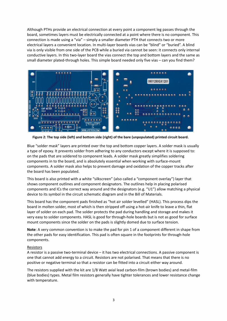
Printed circuit board (PCB) (also called a printed wire board, PWB) The printed circuit board supplied with the kit (Figure 1) is a 1.1 mm thick double‐sided through‐hole board with plated‐through holes. “Double‐sided” means that there are copper circuit connections (tracks) on the top and bottom of the board, but no internal conductive layers within the board. More advanced circuit boards can have multiple (up to 24) internal copper layers. The insulating material in between the conductive copper layers is a type of fibreglass. “Plated‐through‐holes” (PTH) means that during the process of manufacturing the PCB holes are drilled through the fibreglass board and then a layer of copper is electroplated on the cylindrical surface of these holes, electrically connecting (in this case) the top and bottom copper layers at each hole. The cylindrical metallic surface on the interior of each hole can easily be seen.
3
Although PTHs provide an electrical connection at every point a component leg passes through the board, sometimes layers must be electrically connected at a point where there is no component. This connection is made using a “via” – simply a smaller diameter PTH that connects two or more electrical layers a convenient location. In multi‐layer boards vias can be “blind” or “buried”. A blind via is only visible from one side of the PCB while a buried via cannot be seen: it connects only internal conductive layers. In this two‐layer board the vias connect the top and bottom layers and the same as small diameter plated‐through holes. This simple board needed only five vias – can you find them?
Figure 2: The top side (left) and bottom side (right) of the bare (unpopulated) printed circuit board.
Blue “solder mask” layers are printed over the top and bottom copper layers. A solder mask is usually a type of epoxy. It prevents solder from adhering to any conductors except where it is supposed to: on the pads that are soldered to component leads. A solder mask greatly simplifies soldering components in to the board, and is absolutely essential when working with surface‐mount components. A solder mask also helps to prevent damage and oxidation of the copper tracks after the board has been populated.
This board is also printed with a white “silkscreen” (also called a “component overlay”) layer that shows component outlines and component designators. The outlines help in placing polarised components and ICs the correct way around and the designators (e.g. “U1”) allow matching a physical device to its symbol in the circuit schematic diagram and in the Bill of Materials.
This board has the component pads finished as “hot air solder levelled” (HASL). This process dips the board in molten solder, most of which is then stripped off using a hot‐air knife to leave a thin, flat layer of solder on each pad. The solder protects the pad during handling and storage and makes it very easy to solder components. HASL is good for through‐hole boards but is not as good for surface mount components since the solder on the pads is slightly domed due to surface tension.
Note: A very common convention is to make the pad for pin 1 of a component different in shape from the other pads for easy identification. This pad is often square in the footprints for through‐hole components.
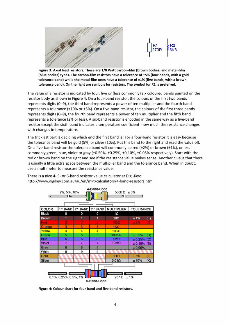
Resistors A resistor is a passive two‐terminal device – it has two electrical connections. A passive component is one that cannot add energy to a circuit. Resistors are not polarised. That means that there is no positive or negative terminal so that a resistor can be fitted into a circuit either way around.
The resistors supplied with the kit are 1/8 Watt axial lead carbon‐film (brown bodies) and metal‐film (blue bodies) types. Metal film resistors generally have tighter tolerances and lower resistance change with temperature.
4
Figure 3: Axial lead resistors. These are 1/8 Watt carbon‐film (brown bodies) and metal‐film (blue bodies) types. The carbon‐film resistors have a tolerance of ±5% (four bands, with a gold tolerance band) while the metal‐film ones have a tolerance of ±1% (five bands, with a brown tolerance band). On the right are symbols for resistors. The symbol for R1 is preferred.
The value of a resistor is indicated by four, five or (less commonly) six coloured bands painted on the resistor body as shown in Figure 4. On a four‐band resistor, the colours of the first two bands represents digits (0–9), the third band represents a power of ten multiplier and the fourth band represents a tolerance (±10% or ±5%). On a five‐band resistor, the colours of the first three bands represents digits (0–9), the fourth band represents a power of ten multiplier and the fifth band represents a tolerance (2% or less). A six‐band resistor is encoded in the same way as a five‐band resistor except the sixth band indicates a temperature coefficient: how much the resistance changes with changes in temperature.
The trickiest part is deciding which end the first band is! For a four‐band resistor it is easy because the tolerance band will be gold (5%) or silver (10%). Put this band to the right and read the value off. On a five‐band resistor the tolerance band will commonly be red (±2%) or brown (±1%), or less commonly green, blue, violet or gray (±0.50%, ±0.25%, ±0.10%, ±0.05% respectively). Start with the red or brown band on the right and see if the resistance value makes sense. Another clue is that there is usually a little extra space between the multiplier band and the tolerance band. When in doubt, use a multimeter to measure the resistance value.
There is a nice 4‐ 5‐ or 6‐band resistor value calculator at Digi‐Key: http://www.digikey.com.au/au/en/mkt/calculators/4‐band‐resistors.html
Figure 4: Colour chart for four band and five band resistors.

5
Capacitors
A capacitor is a passive two‐terminal device. The board uses two types of capacitor: ceramic capacitors which are the small orange‐brown disk components and electrolytic capacitors which are the black cylindrical components.
Figure 5 left: Capacitors: Electrolytic radial lead (left) and ceramic radial lead types (right). Note that electrolytic capacitors are polarised. The longer lead is the positive one. On the right are symbols for capacitors. C1 and C2 are polarised types; C3 is unpolarised.
Electrolytic capacitors are polarised; they have a positive terminal and a negative terminal and must be connected the correct way. If they are connected with reverse polarity they will not work, and some types (particularly tantalum capacitors) may explode. The polarity of an electrolytic capacitor is marked on the case with a stripe and/or a negative sign denoting the negative terminal and/or the shorter of the two leads denoting the negative terminal. The smaller electrolytic capacitor is marked 10μF 25V and the larger one with 100 μF 16V.
Ceramic capacitors are not polarised; they can be connected either way around. The smaller ceramic capacitors are marked “22”. This is read as 22 pF (pico Farad). One Farad is a lot of capacitance, so capacitor values are usually small. One pF is 1 x 10‐12 Farad, sometimes called a “puff”... The larger ceramic capacitors are marked “104”. This is read as 10 x 104 pF = 105 pF = 102 nF = 100 nano Farad.
Diode One diode (a very common 1N4001) is used to protect the circuit against connecting a power source the wrong way around. A diode is a polarised two‐terminal device: it has a positive terminal (the anode) and a negative terminal (the cathode). The cathode is marked with a stripe on the device – the stripe resembles the line on the diode symbol.
Figure 6: Axial lead diode (left) and symbol (right). The stripe around the body of the diode indicates the negative terminal, or cathode.
Crystal A packaged crystal (and two capacitors, C1, C2) is needed to produce a clock signal that allows the microcontroller to operate, and to operate at a precise clock frequency. A crystal is a passive two‐terminal device. It is literally a very precisely sized block of piezoelectric quartz with electrical terminals connected to two parallel faces. Piezoelectric quartz has the useful property of producing a charge across its faces when compressed, and vice‐versa. This allows oscillation at a precise frequency. The crystal in the kit is cut to 12.000 MHz and packaged in a HC49 case.
6
Figure 7: Crystal in HCM49 package (left) and symbol (right).
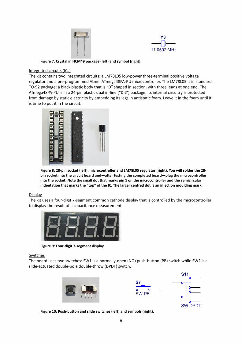
Integrated circuits (ICs) The kit contains two integrated circuits: a LM78L05 low‐power three‐terminal positive voltage regulator and a pre‐programmed Atmel ATmega48PA‐PU microcontroller. The LM78L05 is in standard TO‐92 package: a black plastic body that is “D” shaped in section, with three leads at one end. The ATmega48PA‐PU is in a 24‐pin plastic dual in‐line (“DIL”) package. Its internal circuitry is protected from damage by static electricity by embedding its legs in antistatic foam. Leave it in the foam until it is time to put it in the circuit.
Figure 8: 28‐pin socket (left), microcontroller and LM78L05 regulator (right). You will solder the 28‐pin socket into the circuit board and—after testing the completed board—plug the microcontroller into the socket. Note the small dot that marks pin 1 on the microcontroller and the semicircular indentation that marks the “top” of the IC. The larger centred dot is an injection moulding mark.
Display The kit uses a four‐digit 7‐segment common cathode display that is controlled by the microcontroller to display the result of a capacitance measurement.
Figure 9: Four‐digit 7‐segment display.
Switches The board uses two switches: SW1 is a normally‐open (NO) push‐button (PB) switch while SW2 is a slide‐actuated double‐pole double‐throw (DPDT) switch.
Figure 10: Push‐button and slide switches (left) and symbols (right).
7
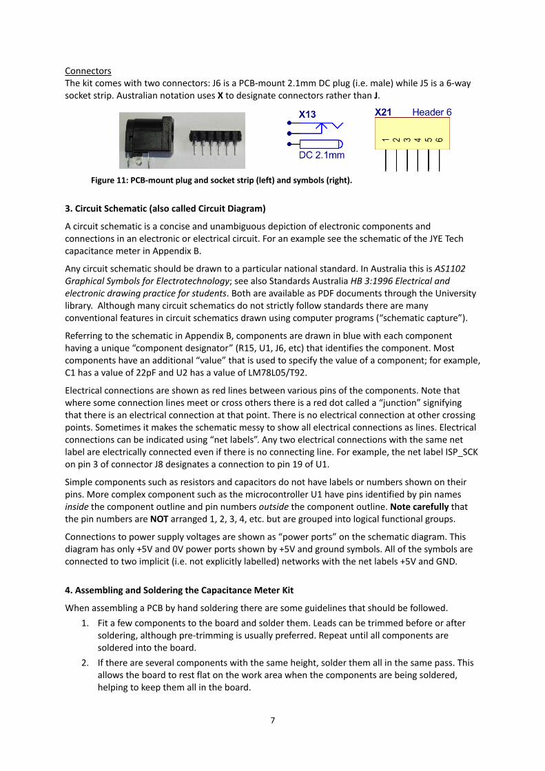
Connectors The kit comes with two connectors: J6 is a PCB‐mount 2.1mm DC plug (i.e. male) while J5 is a 6‐way socket strip. Australian notation uses X to designate connectors rather than J.
Figure 11: PCB‐mount plug and socket strip (left) and symbols (right).
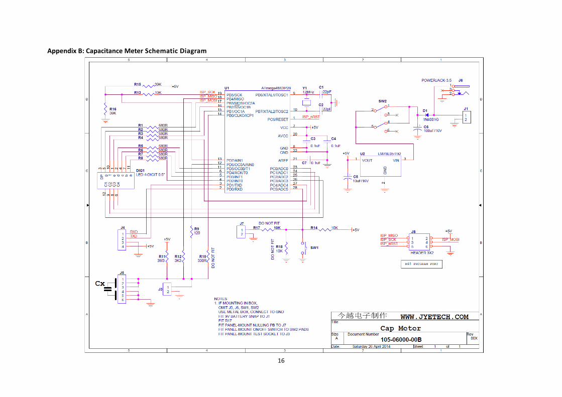
3. Circuit Schematic (also called Circuit Diagram)
A circuit schematic is a concise and unambiguous depiction of electronic components and connections in an electronic or electrical circuit. For an example see the schematic of the JYE Tech capacitance meter in Appendix B.
Any circuit schematic should be drawn to a particular national standard. In Australia this is AS1102 Graphical Symbols for Electrotechnology; see also Standards Australia HB 3:1996 Electrical and electronic drawing practice for students. Both are available as PDF documents through the University library. Although many circuit schematics do not strictly follow standards there are many conventional features in circuit schematics drawn using computer programs (“schematic capture”).
Referring to the schematic in Appendix B, components are drawn in blue with each component having a unique “component designator” (R15, U1, J6, etc) that identifies the component. Most components have an additional “value” that is used to specify the value of a component; for example, C1 has a value of 22pF and U2 has a value of LM78L05/T92.
Electrical connections are shown as red lines between various pins of the components. Note that where some connection lines meet or cross others there is a red dot called a “junction” signifying that there is an electrical connection at that point. There is no electrical connection at other crossing points. Sometimes it makes the schematic messy to show all electrical connections as lines. Electrical connections can be indicated using “net labels”. Any two electrical connections with the same net label are electrically connected even if there is no connecting line. For example, the net label ISP_SCK on pin 3 of connector J8 designates a connection to pin 19 of U1.
Simple components such as resistors and capacitors do not have labels or numbers shown on their pins. More complex component such as the microcontroller U1 have pins identified by pin names inside the component outline and pin numbers outside the component outline. Note carefully that the pin numbers are NOT arranged 1, 2, 3, 4, etc. but are grouped into logical functional groups.
Connections to power supply voltages are shown as “power ports” on the schematic diagram. This diagram has only +5V and 0V power ports shown by +5V and ground symbols. All of the symbols are connected to two implicit (i.e. not explicitly labelled) networks with the net labels +5V and GND.
4. Assembling and Soldering the Capacitance Meter Kit
When assembling a PCB by hand soldering there are some guidelines that should be followed.
1. Fit a few components to the board and solder them. Leads can be trimmed before or after soldering, although pre‐trimming is usually preferred. Repeat until all components are soldered into the board.
2. If there are several components with the same height, solder them all in the same pass. This allows the board to rest flat on the work area when the components are being soldered, helping to keep them all in the board.

8
3. Solder components that sit closer to the board (lower mounted height) before components that sit further away from the board (higher mounted height). For surface mount components this prevents tall components from interfering with the soldering iron when soldering surface‐mount or other short components.
4. If a board has a difficult‐to‐solder expensive component(s), solder this component first and test it if you can before soldering any more components. This avoids extra work if the expensive component or board is damaged in soldering.
5. Once all components that can be “washed” are soldered in, remove the soldering flux residue from the board. This is called de‐fluxing. Different solvents are used to remove different types of flux.
6. Some components, typically potentiometers, switches and connectors, are not sealed and therefore are not protected against the solvents that are used to remove soldering flux. These are soldered in after de‐fluxing.
7. Carefully inspect all solder joints on the board and then test it.
In production, soldering is done by solder wave or reflow soldering machines that effectively solder all components at the same time so these rules don’t apply. De‐fluxing also occurs in machines. Some components have seals that are removed after the de‐fluxing stage; otherwise, non‐washable components are hand soldered after machine de‐fluxing. There are many stages in production soldering that are not described here.
Practice Soldering 1. Do not open the Capacitance Meter Kit yet!
2. You will use the eight 1K0 resistors (brown, black, red, gold) supplied separately to practice with by soldering them into a small piece of strip board.
3. The standard length of a 1/4 W axial lead resistor is 0.4 inches, or the distance between five holes in the strip board. The legs of the resistor need to be bent to fit this distance. Centre a resistor on five holes in the strip board to judge where its legs should be bent. Use long nose flat‐jaw pliers to bend one leg at 90 degrees at the correct place. The leg is tin‐plated annealed copper and is very soft – just bend it by pushing with your finger. Put the bent leg in one of the holes in the strip board and grip the other leg with the pliers in a place that will allow the leg to go into the fifth hole when the leg is bent. Withdraw the resistor with the pliers and bend the second leg at 90 degrees. This is called “dressing the legs” of the resistor. Repeat for the other seven 1K0 resistors.
4. Insert four of the 1K0 resistors in adjacent locations in the strip board from the component side (the side without copper strips) ensuring that the gold tolerance bands are all on one side. Non‐polarised components such resistors, inductors and non‐polarised capacitors should always be placed so that they can easily be read from the bottom of the board and from one side of the board.
5. With four resistors correctly inserted from the component side of the strip board, turn the board over and bend the resistor leads by about 30 degrees to hold them in place. Avoid folding the component leads flat on the board since this would make them difficult to de‐solder if necessary in the future.
6. Turn the strip board over so the leads are facing up. Solder the leads one at a time to the board and cut off surplus leads close to the board.
7. Now use the other four resistors to repeat steps 4 and 5. Once the leads have been bent at about 30 degrees, trim them to no longer than 1.5 mm above the board. Then solder the leads to the board.
Comment: Although it is more difficult, there are good reasons why component leads should be trimmed to length before soldering. See the comment at assembly step 4 below.
9
Assembly sequence In the instructions below it is assumed that you have the silkscreen printing uppermost and the board oriented so the text “WWW.JYETECH.COM” is in the bottom right hand corner.
Note that the completed board will have three unpopulated (empty) resistor locations (R10, R17, R18), and five unpopulated connectors (J1, J3, J4, J7, J8) as discussed in section 8 below.
1. Open the Capacitance Meter Kit and begin by identifying all of the components. A good method is to write the component designators, spread out on a piece of paper and then place the component on the designator once it is identified. Note that there are multiples of some components. For example, there are eight 680R resistors, R1 to R8.
2. Start with resistors R1 to R8, located below the 7‐segment display area DIG1. The 1K5 resistors usually supplied in the kit have been replaced with 680R resistors (blue, grey, black, black, brown) so that the LED display is brighter.
3. Dress the legs of R1 to R8 and insert them into the board, making sure that they are all inserted the same way around, and that the gold tolerance band is on the right when viewed from the right side of the board. That is, when you turn the board sideways so that the component designators R1, R2, R3, etc. are the correct way up, each resistor should be oriented for correct reading of the bands from left to right.
4. With resistors R1 to R8 correctly inserted from the front of the board, turn the board over and bend the resistor leads by about 30° to hold them in place. Solder the leads one at a time to the board and cut off surplus leads close to the board: within about 1.5 mm.
Comment: High quality soldering to IPC class 3 prescribes that the trimmed leads protrude no more than 1.5mm from the surface of the board. The leads should be trimmed to length before soldering in this case so that there is no risk of cutting the solder fillet or fracturing the joint between the solder and the lead by trimming the leads after soldering. If component leads are trimmed after soldering, all IPD classes require visual inspection at 10x magnification of every solder joint to ensure that no solder joint fractures have occurred.
5. Next dress, insert, solder and trim (or trim and solder) the remaining resistors. These are all located below the display area, DIG1
R1 – R8: 680R (±1%) blue body, blue, grey, black, black, (brown)
R9: 120R (±5%) tan body, brown, red, brown, (gold)
R11: 3M3 (±1%) blue body, orange, orange, black, yellow, (brown)
R12: 3K3 (±1%) blue body, orange, orange, black, brown, (brown)
R13, R14: 10K (±1%) blue body, brown, black, black, red, (brown)
R15, R16: 39K (±1%) blue body, orange, white, black, red, (brown).
Note: There should be no resistor fitted in the positions for R10, R17 and R18.
6. Insert the SIL socket J5 (do not bend the pins to retain the component) and turn the board over. Make sure the socket is still fully inserted and solder the two end pins. Check that the socket is pressed against the board and correct if required. Solder the remaining pins. There is no need to trim the pins.
7. Now insert and solder the 12MHz crystal, Y1. Bend the leads out slightly to hold the component in place, turn the board over, solder the crystal and trim off excess leads.
8. Insert 22 pF capacitors C1 & C2. These are the small orange/brown discs with 22 on the side and a black band on the top of the capacitor. Bend the leads slightly to hold them in place.
9. Now insert 0.1 μF capacitors C3, C4 & C7. They are small orange/brown discs with 104 on the side. Capacitor C3 is inserted to the left of the crystal and left of C1. Capacitors C4 & C7 are located in the middle of the board. Bend the leads slightly to hold the capacitors in place and then turn the board over. Solder the capacitors and remove excess leads.
10. Insert 1N4007 diode D1 near the top right hand corner of the PCB. The white band of the

10
diode goes downwards matching the white band on the silkscreen. Bend the leads slightly to hold the diode in place and turn PCB over. Solder the diode and remove excess leads.
11. Insert the LM78L05 regulator U2, aligning the flat side of the regulator with the flat on the silkscreen. Bend the leads outwards slightly to hold U2 in place, turn the board over and solder. Remove excess leads.
12. See note below. Insert the two electrolytic capacitors C5 (10 μF) and C6 (100 μF). These are about 8mm long and 4mm/6.5mm diameter. On the side of the two capacitors you will see a white stripe: the lead on that side is the negative one and the other (longer) lead is the positive lead. Important! Electrolytic capacitors are polarised. Make sure that the long lead (positive) is inserted in the hole with the square pad (pin 1). Bend the leads to hold the components in place then turn the board over and solder the capacitors. Trim surplus leads.
NOTE! If you are going to mount the PCB in a box with the display flush then you will need to mount them on the other side of the board or bend them over as they are higher than the display. When bending the capacitors over make sure that the leads do not short together. See section 9 of this document.
13. See note below. Carefully insert SW1 and SW2 then turn the PCB over and solder the switches. Note that the footprint of the push button switch is rectangular not square.
NOTE! If you are going to mount the PCB in a box with the display flush then do not mount SW2; see section 9 of this document.
14. Insert the 28‐pin socket for the microcontroller in U1, ensuring that the indentation on the socket matches the indentation on the silkscreen (pointing to the word ZERO). DIL sockets are easiest to solder if you tack two diagonal corners, making sure that the socket is flat against the PCB, and then solder all pins. Do not insert the microcontroller in the socket yet.
15. See note below. If you intend to use the on‐board power socket J6 then carefully insert it. It goes to the right of the display area near diode D1. Turn the board over and solder the pins.
NOTE! If you are going to mount the PCB in a box with the display flush then do not mount J6; see section 9 of this document.
16. Carefully insert the LED display with the decimal points facing towards the line of resistors. You may find that the leads need a little straightening to line up with holes in the PCB. Turn the PCB over and solder the leads, ensuring that the LED display remains flush with the PCB. Use the diagonal tacking technique from step 15. Trim the leads close to the board.
17. Now de‐flux the board using the technique demonstrated by your tutor and carefully inspect each solder joint. Inspection is much easier once the residual flux has been removed from the board. Always visually inspect each solder joint. Every solder joint should be smooth and shiny (or at least satin), with a concave fillet between the pad on the PCB and the component lead showing that the molten solder has correctly wet both board and lead on both sides of the board. Any dull or crinkly uneven joints will need to be re‐soldered by using “solder wick” to remove most of the existing solder and then re‐soldering.
Comment: See NASA document on through‐hole soldering workmanship for inspection details. We do not expect you to be able to solder to IPC Class 3 but you do need to understand what good and bad solder joints look like.
18. The soldering is now complete and the capacitance meter ready for testing.
If you are going to mount the board in a box you should now temporarily connect the off‐board switches that you are going to use by soldering them to discrete wires so that the meter can be tested before putting it into the box.

11
5. About Flux and Flux Removal
Soldering flux has a vital but difficult job to do. The purpose of a soldering flux is (a) to clean impurities and oxides, particularly copper oxide, from metal parts to be soldered; (b) to exclude air (oxygen) from the solder joint and (c) to lower the surface tension of the molten solder. All of these improve solder wetting. Solder flux must therefore become chemically active at a temperature lower than the melting point of solder. When a flux is activated by heating (usually around 100°C) it becomes a highly effective reducing agent. It is so reactive that it can strip oxygen atoms that have already bonded with copper, converting copper oxide to metallic copper.
Solder wire for electronics use contains a core of dry powdered resin [US rosin] which may have additives. Two types of resin flux are used: RMA (resin mildly activated) is the most common and RA (resin activated) is also used. Resin fluxes become active at about 100°C, well under the melting point of solder. Both types must be removed after soldering as they contain acidic substances (particularly RA) that would corrode the PCB.
Other types of solder flux are used in different situations: no‐clean flux – as its name says, you just leave it on; low solids flux completely evaporates if the (wave) soldering process is correctly controlled; water soluble flux must be removed (using hot water) because it is hygroscopic and leaves a conductive residue on the board.
Solder manufacturers also manufacture solvents specifically to remove their fluxes. Multicore manufactures MCF800 solvent for cleaning residues from its 309 flux. MCF800 contains glycol ethers and can be used by itself, in aqueous solution, and/or with subsequent alcohol or de‐ionised water washes. In general, de‐fluxing solvents contain a range of quite aggressive organic solvent. They are effective but unpleasant to work with, typically requiring breathing, eye and skin protection.
Isopropyl alcohol (2‐Propanol, also called Isopropanol or IPA) is a common solvent used for a range of electronics cleaning purposes, including de‐fluxing. Isopropanol does not attack plastics and is relatively safe for people to use. When Isopropanol is used for de‐fluxing, mechanical scrubbing with a stiff bristle brush is also required, and it is essential to remove flux soon after soldering.
You will use Isopropanol and a bristle brush for de‐fluxing in the Lab.
6. Checking and Testing your Meter
Next, inspect the assembly very carefully before applying power – you don’t want to ruin your hard work because of a simple error. Check
Is the diode inserted the correct way, with the stripe downwards?
Are the two electrolytic capacitors inserted the correct way, with the negative terminals in the round pads?
Is the LM78L05 regulator inserted the correct way, matching the silkscreen?
Is the IC socket inserted the correct way, with the indentation to the left?
Is the 7‐segment display inserted the correct way, with the decimal points downwards?
Are all resistors in the correct places?
Check all pads for pins that you have forgotten to solder (it happens!)
Check carefully on the bottom and top of the board for solder splatter shorting across connections. The magnifying glass on the “helping hands” is useful.
If you find anything wrong, such as a component inserted backwards or in the wrong place, ask a tutor to show you how to safely remove the component and re‐solder it.
Do not insert the microcontroller in its socket yet.
First check the +5V power supply rail on the board for short circuits to ground. It will be helpful to refer to the circuit schematic in Appendix B.
12
1. Using a digital multimeter (DMM) set to resistance, measure that resistance between pin 1 of the LM78L05 regulator U2 and GND. Pin 1 is the left‐most pin of U2 when looking from the bottom of the board. A suitable GND reference point is pin 2 (round pad) on either J1 or J7. You should measure at least several thousand Ohms. If the resistance is zero or close to it there is a short circuit between +5V and GND somewhere on the board. You will need to find and remove the short before proceeding.
Next check the supply voltage, on‐off switch and +5 V power supply as follows. 2. Disable the power supply output, set the voltage to 10.0 V and the current limit to 0.10 A. 3. Use the supplied banana plug to 2.1 mm socket lead to connect the lab power supply to the
connector J6. If you haven’t populated J6, ask for an alligator clip lead to connect to the wires that you soldered on to connector J1.
4. Enable the power supply output. If the green Constant Voltage light immediately changes to a red Constant Current light the 50 mA current limit that you have set has been reached and something is wrong: turn off the power supply immediately. There is probably a short circuit between the supply voltage and ground somewhere on the PCB.
5. If everything seems OK, then use a digital multimeter (DMM) set to DC Volts to measure the supply voltage at the input to switch SW2 with the switch in the OFF position. A convenient place to measure this voltage is on the cathode lead of diode D1. When you measure a voltage you are always measuring it relative to some other (reference) voltage level. A suitable reference voltage is GND, or 0 V, on the circuit; a convenient GND reference point is pin 2 on either J1 or J7. You should measure about +9.3 V (i.e. about 0.7 V less than the 10.0 V supply) on the cathode of D1 relative to GND. If the supply voltage is less than 8.0 V the regulator may not operate correctly.
6. Next, measure the output voltage on pin 1 of the LM78L05 regulator U2. Pin 1 is the left‐most pin of U2 when looking from the bottom of the board. You should measure 0 V when SW2 is OFF and +5.0 V when SW2 is ON.
7. Measure the voltage on pins 7 and 20 of the microcontroller socket U1. The pins on a dual in‐line IC are numbered beginning with pin 1 on the top left of the IC (square pad) down the left side, across to the bottom right pin and then up to the top right. Pins 7 and 20 are the +5 V power supply pins for the microcontroller so you should measure 0 V when SW2 is OFF and about +5.0 V when SW2 is ON. Pins 8 and 22 are the +0 V power supply pins for the microcontroller so you should measure 0 V regardless of the state of SW2.
Now that you have ensured that the power supply to the microcontroller socket U1 is correct, turn off the power at the lab supply. If you insert or remove a semiconductor device with power turned on, it is likely that the electronic component will be destroyed.
8. Now you can insert the microcontroller in its socket. It is very likely that you will need to bend all pins on both sides of the IC slightly inwards so that they will easily fit into the socket. Use flat‐jaw long‐nose pliers to do this, bending all pins on one side at the same time.
9. Fit the IC into the socket, checking that all pins are correctly started in their individual sockets. Then carefully push the IC into the socket.
10. Turn on the lab power supply and your capacitance meter should be working. 11. Pressing and releasing the push button SW1 will cause the microcontroller to measure the
capacitance with no test capacitor connected. This will measure the stray capacitance of the circuit itself and store the value in the microcontroller’s EEPROM. After some seconds a reading of 000P should appear on the 7‐segment display.
12. You can use known capacitances to check that the meter works and auto‐ranges. 13. To check the absolute accuracy you would need capacitors of at least 0.1% accuracy but you
will get a good feel for the instrument by checking with normal close tolerance capacitors such as 1% silver mica.

13
7. Fault finding
If you have followed the instructions carefully your meter should work first time, but people make mistakes and components may be faulty when supplied or damaged during assembly. To find out why your meter is not working use a digital multimeter (DMM) and/or an oscilloscope.
You should have tested the supply voltage connector, on‐off switch and +5 V regulator U2 before inserting the microcontroller in its socket. If you didn’t, shame on you for taking a shortcut. Remove the microcontroller from its socket and do those tests now. Following are some other tests that should show up most of the common faults. Follow them through step by step until you find the fault. In the following, all voltage measurements are made with a DMM or oscilloscope relative to GND on the board.
1. Check that the microcontroller U1 is inserted the correct way around. Check that none of the pins is bent over outside its socket or shorting with another pin. Check for solder shorts around U1 on the underside of the PCB. Check that all pins have been soldered.
2. If the display is not functioning correctly, first check that you have the display in the correct way round. Check that there are no shorts around the display pins on the underside of the board. Check that all pins have been soldered. Check all connections related to the LED display. Look for opens as well as shorts.
3. If there is still no display (or garbage display without activity)
First power supply should be checked again. Make sure that +5V is available at microcontroller power pins (pins 7 & 20 of U1).
If power supply is good, check that the microcontroller is being clocked. The best way to check is to probe the microcontroller’s oscillator output pin (pin 10 of U1) with an oscilloscope. You should see a quasi‐sinusoidal oscillation of around 500 mV peak to peak at a frequency of 12 MHz. This check can be done less well by measuring the DC voltage at pin 10 of U1. It should read about 350 mV if the oscillator is working. If not, Yl, Cl, C2 and the microcontroller U1 should be checked. Usually this problem is caused by defective Y1I, C1 or C2. An un‐programmed or incorrectly programmed microcontroller can cause this problem too.
4. If the display is stuck at "CO " when the zeroing button is pressed
Check R11, R13, R15, R16 and related connections.
Check that J5 pins 1, 2, and 3 are not shorted to GND.
5. Bad serial data output
Make sure that an RS232 level converter is being used if connected to a standard RS232 device. This converter, for example a MAX232 IC, changes 0V and +5V signals to +10V and ‐10V signals.
Make sure that correct data format is selected on the receiving device.
8. What about the unpopulated parts?
When assembled according to these instructions the board has several component places that are unpopulated (i.e. components not fitted). Q: Why would a circuit board be designed with places for unused parts? A: Because the circuit board can then be used in more flexible ways and additional cost is essentially zero. To understand how these ‘extra’ parts could be used, refer to the circuit schematic.
Connector J1 can be used instead of J6 to provide power to the circuit by using a 9V battery and a “battery snap” connector such as Jaycar part number PH9230, $0.40. This would make the capacitance meter completely portable.
Connector J3 can be used instead of J5 to connect to an external capacitor test point if the PCB is mounted in a box.

14
Connector J4 can be populated with header pins or sockets for serial output at TTL levels of the capacitance readings. TTL levels are nominally 0V for a logic 0 and +5V for a logic 1. You will be able to see this output by using an oscilloscope to probe the TXD pin relative to GND. With the addition of an RS232 level‐shifter circuit (not supplied) you could transform the TTL levels into ±10V RS232 levels and display the serial output of the capacitance meter on a computer terminal.
Connector J7 can be used to connect to an external Zero push button instead of SW1 if the PCB is mounted in a box.
Connector J8 is an in‐circuit programming connector for the Atmel ATMega microcontroller.
The three unused resistors are:
Resistor R10 is connected between U1 pin 14 (the microcontroller’s PB0/CLKO/ICP1 pin) and the positive terminal of the test socket J5. Its function is not obvious, although it may have been used when the program that runs on U1 was being developed and tested. Do not fit.
Resistor R17 is required only if an external Zero push button is used instead of SW1.
Resistor R18 is required only if an external Zero push button is used instead of SW1.
9. Mounting your meter in a box
If you plan on keeping and using your capacitance meter it should be mounted in a box to protect it. To achieve the best accuracy the box should be metal and the GND side of the component test connector connected to the box. You should make the following modifications for ease of use when the meter is mounted in a box.
The electrolytic capacitors C5 and C6 are too tall and will interfere with the box lid. You can place them on the back side of the board or leave the leads long enough to allow the capacitors to be bent over and rest sideways on the board.
Do not fit the power socket J6 since it will interfere with the box lid. Fit a PP3 battery snap to J1 instead, so your meter can be powered by a 9V battery.
Do not fit the power switch SW2 since you will need a power switch on the outside of the box. Instead, source a suitable panel‐mount switch, fit it to the lid of the box and run wires to terminals 1 and 2 of the footprint SW2 on the PCB.
Source a suitable panel‐mount normally‐open push button, fit it to the lid of the box and run wires to terminals 1 and 2 of the footprint J7 on the PCB. You can leave SW1 in place
Mount the circuit board to the underside of the box lid with 8mm long standoffs. This will place the top of the 7‐segment display just below the outside of the box lid.
Acknowledgement These notes draw from a document written by Charles Ivermee [1] and used with his permission.
References
1. C. Ivermee. Capacitance Meter. Electronic document http://www.radiowymsey.org/capmeter.htm, accessed 29 March 2014.
2. Williams, T. Circuit Designer's Companion. Butterworth Heinmann, Kent, 1991. 621.3815/118 3. MTRX1701 Workshop Technology – Soldering Lab.
http://www.aeromech.usyd.edu.au/MTRX1701/Course Material/Soldering/
David Rye
April 2014; revised 15 April 2015.

15
Appendix A: Capacitance Meter Bill of Materials (P/N: 102‐06001‐04)
Designator Type Value Qty Package Remarks
C1, C2 Capacitor 22pF, ceramic 2 [CR200] Marking 22
C3, C4, C7 Capacitor 0.1uF, ceramic 3 [CR200] Marking 104 = 10 x 104 pF
C5 Capacitor 10uF/16V, electrolytic 1 [CAPPR_025X060]
C6 Capacitor 100uF/16V, electrolytic 1 [CAPPR_035X080]
DIG1 LED 7‐segment LED, 4‐Digit 0.5", common cathode, red 1 [DIG_4‐0.5"]
D1 Diode 1N4001G 1 [DO41] 1N4007 actually supplied
J5 Socket 6‐pin single row socket, 2.54 mm (0.1”) pitch 1 [HD1001X6]
J6 Connector DC005, 2.1mm core 1 [POWERJACK‐3.5]
R1, R2, R3, R4, R5, R6, R7, R8
Resistor 680R 1% 8 [RAXIAL400] The 1K5 resistors usually supplied with the kit are replaced with 680R for a brighter display.
R9 Resistor 120R 5% 1 [RAXIAL400] brown, red, brown, gold
R11 Resistor 3M3 1% 1 [RAXIAL400] orange, orange, black, yellow, brown
R12 Resistor 3K3 1% 1 [RAXIAL400] orange, orange, black, brown, brown
R13, R14 Resistor 10K 1% 2 [RAXIAL400] brown, black, black, red, brown
R15, R16 Resistor 39K 1% 2 [RAXIAL400] orange, white, black, red, brown
SW1 Switch Tactile NO PB switch, 6 x 6 x 8 mm 1 [SW_TACT_4X6]
SW2 Switch DPDT switch, SK‐22D02P 1 [SW_2T2P_2MM]
U1 IC ATmega48 / DIP28 1 [DIP28‐300]
U2 IC LM78L05 / T92 1 [TO‐92]
Y1 Crystal 12 MHz 1 [XTAL_HCM49]
PCB PCB 109‐06000‐00B 1 —
Firmware 113‐06003‐010 1 — http://www.jyetech.com/Products/CapMeter/Firmwares_060.php
Note: 1. Do not install components not listed in this BOM. 2. Use component values as specified in this BOM.
Pedagogical note: The ‘Package’ name will depend on which program is used to produce the PCB layout. This name denotes the ‘footprint’ of the component: that is, the pattern of holes, pads on the bottom (and sometimes top) copper layer and the markings on the top (and sometimes bottom) silkscreen layer that suit the particular component. These package names are probably from Eagle PCB.
16
Appendix B: Capacitance Meter Schematic Diagram
17
Appendix C: Capacitance Meter Operating Instructions
Measurement Insert the capacitor to be tested into J5. The capacitance will be displayed. Alternatively capacitors not fitting into J5 can be connected through J3 with a pair of clips. It will take a longer time to show results for larger capacitors but the time should not be longer than 2 seconds.
Zeroing Remove capacitor (if any) from J5 and J3. Press the "ZERO" button and "CO " will be displayed. Wait for it to disappear. The stray capacitance has now been measured and compensated. The compensation value is stored in the microcontroller’s EEPROM and will remain in effect until another zeroing is performed.
Shielding is required to obtain good measurement results for small capacitances. Mount the board into a metal box and connect the ground of the meter to the enclosure.
Serial Data Output Format The ASCII output from TXD pin of J4 contains three fields: sequence number, measurement time (in seconds), and measured capacitance. The line format is as below.
SSSSS TTTTT.tt CCCCU
where SSSSS is a 5 digit sequence number, TTTTT.Tt is an 8 digit time stamp (in seconds),
and CCCCU is a 5 digit measured capacitance with U being unit digit. The fields are separated
by one space character (0x20). Each line terminates with line feed (0x0A) and carriage return (0x0D) characters.
Output baud rate is 38400bps; data format is 8 data bits, 1 stop bit, and no parity.
The output voltages are TTL (0V / 5V) levels, not RS232 (+10 / ‐10V) levels, so a level converter is needed to connect to a RS232 compatible device such as a PC serial port.
Specifications
Range: 1 pF – 500 μF
Power Supply voltage: 8 ‐ 16 DC
Power Supply current: < 30mA