multi-bit delta-sigma modulation technique for fractional...
TRANSCRIPT

MULTI-BIT DELTA-SIGMA MODULATION TECHNIQUEFOR FRACTIONAL-N FREQUENCY SYNTHESIZERS
BY
WOOGEUN RHEE
B.S., Seoul National University, 1991M.S., University of California at Los Angeles, 1993
THESIS
Submitted in partial fulfillment of the requirementsfor the degree of Doctor of Philosophy in Electrical Engineering
in the Graduate College of theUniversity of Illinois at Urbana-Champaign, 2001
Urbana, Illinois

iii
MULTI-BIT DELTA-SIGMA MODULATION TECHNIQUEFOR FRACTIONAL-N FREQUENCY SYNTHESIZERS
Woogeun Rhee, Ph.D.Department of Electrical and Computer EngineeringUniversity of Illinois at Urbana-Champaign, 2001
Bang-Sup Song, Advisor
Fractional-N frequency synthesis provides agile switching in narrow channel spacing
systems and alleviates phase-locked loop (PLL) design constraints for phase noise and
reference spur. The inherent problem of the fractional-N frequency synthesizer is that the
periodic operation of the dual-modulus divider produces spurious tones. Several techniques
have been used to reduce spurious tones. Among those techniques, the delta-sigma
modulation method provides arbitrarily fine frequency resolution and makes the spur-
reduction scheme less sensitive to process and temperature variations since frequencies are
synthesized by the digital modulation.
This thesis proposes a multi-bit∆−Σ modulation technique as a spur reduction method
to enhance the overall synthesizer performance, and the oversampling modulator
performance is analyzed with the consideration of practical design aspects for frequency
synthesizers. A prototype fractional-N frequency synthesizer using a 3-b third-order∆−Σ
modulator has been designed and implemented in 0.5-µm CMOS. Synthesizing 900 MHz
with 1-Hz resolution, it exhibits an in-band phase noise of -92 dBc/Hz at 10-kHz offset with
a reference spur of less than -95 dBc. Experimental results show that the proposed system
is applicable to low-cost, low-power wireless applications and that it meets the
requirements of most RF applications including multi-slot GSM, IS-54, CDMA, and PDC.

iv
ACKNOWLEDGMENTS
I would like to thank my advisor, Professor Bang-Sup Song, for his insightful guidance
and encouragement throughout this research. I was not a good circuit designer at all when
I joined his group, and I still need to learn many things to be so. However, his invaluable
advice has strengthened me to overcome many hardships, and it has been a great
opportunity for me all the time to work with him.
I also thank Professors Ibrahim N. Hajj, Dilip V. Sarwate, and Naresh Shanbhag, my
committee members, for their generous availability and kind patience, even though I had
difficulty communicating with them out of the campus.
I extend my thanks to supervisors and many engineers in RF IC design group at
Conexant Systems for their help in the prototype chip design, layout, and testing. I wish to
thank Frank Carr (who is now at Broadcom), Akbar Ali, Stephen L. Lloyd, and Mohy F.
Abdelgany for their support in fractional-N frequency synthesizer project; David Tester for
VHDL design; Truong Q. Tran and Frank J. In’tveld for the IC layout; and Ron E. Hlavac
for the board layout. In particular, I wish to thank Akbar Ali, my supervisor, who gave
strong interest and support in my work. I also thank Kwang-Young Kim, my senior friend,
who is now at Broadcom for encouragement during research. There are many other people
who deserve my thanks. They are professors, fellow students, and friends from the
University of Illinois at Urbana-Champaign.
Finally, I would like to thank my parents, Mr. and Mrs. Soo-Bin Rhee, and to my wife,
Soo-Jung Yang, for their love and endless support throughout my study.

v
TABLE OF CONTENTS
CHAPTER PAGE
1 INTRODUCTION .........................................................................................................1
2 REVIEW OF FREQUENCY SYNTHESIS TECHNIQUES........................................52.1 Frequency Synthesis by Phase-Lock Technique..................................................82.2 Fractional-N Frequency Synthesis.....................................................................102.3 Spur Reduction Techniques in Fractional-N Frequency Synthesis....................12
2.3.1 DAC estimation method.........................................................................132.3.2 Random jittering method.......................................................................142.3.3 ∆−Σ modulation method........................................................................162.3.4 Phase interpolation method....................................................................172.3.5 Phase compensation method..................................................................182.3.6 Phase insertion method..........................................................................22
3 INTERPOLATIVE FREQUENCY DIVISION BY OVERSAMPLING....................243.1 Basic Concept....................................................................................................243.2 Modulator Architectures....................................................................................26
3.2.1 Single-stage high-order modulator........................................................263.2.2 MASH modulator...................................................................................273.2.3 Multi-bit modulator................................................................................29
3.3 Quantization Noise.............................................................................................293.4 Dynamic Range Considerations.........................................................................313.5 Idle Tones...........................................................................................................333.6 Stability ..............................................................................................................34
4 HIGH-ORDER∆−Σ MODULATOR WITH MULTI-LEVEL QUANTIZER ...........364.1 Multi-Bit Oversampling Modulator...................................................................364.2 Design of Single-Stage High-Order∆−Σ Modulator.........................................39
4.2.1 Choice of NTF.......................................................................................404.2.2 A 3-b 3rd-order modulator design.........................................................41
4.3 Phase Detector Linearity....................................................................................46
5 DESIGN CONSIDERATIONS FOR HIGH SPECTRAL PURITY...........................495.1 Phase Noise........................................................................................................49
5.1.1 Phase noise generation principle............................................................515.1.2 Integrated phase noise............................................................................535.1.3 Effect of frequency division and multiplication on phase noise............535.1.4 Noise generation in frequency synthesizers...........................................54
vi
5.2 Spurious Tones...................................................................................................565.2.1 Spur generation principle.......................................................................575.2.2 Spur generation in frequency synthesizers............................................58
5.2.2.1 Leakage current.......................................................................595.2.2.2 Mismatches in charge pump...................................................615.2.2.3 Timing mismatch in P/FD.......................................................635.2.2.4 Spur by∆−Σ modulator ..........................................................66
5.3 Settling Time ......................................................................................................665.3.1 State variable description of PLL..........................................................675.3.2 Slew rate of PLL....................................................................................685.3.3 Settling time including slew rate............................................................70
5.4 Frequency Accuracy and Resolution.................................................................715.5 PLL Loop Parameter..........................................................................................72
6 IMPLEMENTATION OF A 1.1-GHZ CMOS FREQUENCY SYNTHESIZER.......746.1 System Architecture...........................................................................................756.2 P/FD ...................................................................................................................766.3 Charge Pump......................................................................................................786.4 Frequency Divider ..............................................................................................83
6.4.1 Prescaler.................................................................................................846.4.2 Digital counters......................................................................................87
6.5 Logic Converters................................................................................................876.6 Bias Circuit ........................................................................................................896.7 Multi-Bit Modulator and Control Logic............................................................896.8 Data Interface and Selection Logic....................................................................916.9 Loop Filter .........................................................................................................91
7 EXPERIMENTAL RESULTS.....................................................................................95
8 CONCLUSIONS........................................................................................................105
APPENDIX A PROGRAM LISTING....................................................................107A.1 Behavioral Model Simulation Program for Second-Order PLL................107A.2 Gate-Level PSPICE Program for Third-Order∆−Σ Modulator.................109
REFERENCES.........................................................................................................115
VITA .........................................................................................................................122

1
CHAPTER 1
INTRODUCTION
The demand for low-cost, universal frequency synthesizers is growing as wireless
systems become diversified. Cellular standards for less than 1-GHz frequency-range
applications are summarized in Table 1.1, including advanced mobile phone system
(AMPS), IS-54, code division multiple access (CDMA), personal digital cellular (PDC),
and global system for mobile communications (GSM). Some applications such as general
packet radio service (GPRS) require relatively agile frequency switching to increase the
data rate with a multi-slot operation. Standard frequency synthesizers based on a phase-
locked loop (PLL) have difficulties in meeting various specifications due to the
fundamental trade-off between loop bandwidth and channel spacing. Due to high division
ratio, meeting the noise requirement with integer-N synthesizers is also challenging when
implemented in CMOS. On the other hand, fractional-N techniques provide wide
bandwidth with narrow channel spacing and alleviate PLL design constraints for phase
noise and reference spur. The inherent problem of the fractional-N frequency synthesizer is
that the periodic operation of the dual-modulus divider produces spurious tones. Several
spur reduction techniques have been proposed, and the∆−Σ modulation technique is
considered in this work.
The objective of this work is to develop a practical frequency synthesis technique for
high spectral purity using a∆−Σ modulation method, which is applicable to low-cost
wireless transceivers. The∆−Σ modulation method makes the spur-reduction scheme

2
relatively less sensitive to process and temperature variations since frequencies are
synthesized by the digital modulation. Even though the implementation of the digital∆−Σ
modulators is not as complicated as that of the analog modulators, the frequency
synthesizer with an on-chip modulator suffers from high power consumption and less-than-
expected noise performance. For those reasons, low-cost fractional-N frequency
synthesizers having an on-chip modulator are hardly found in commercial handset
applications. In this work, the oversampling modulator performance is analyzed by
considering practical design aspects in fractional-N frequency synthesis, and a multi-bit
high-order∆−Σ modulator is proposed to enhance the overall performance.
Table 1.1 Summary of 1-GHz cellular standards.
AMPS
Frequency
Access
Number
Channel
Modulation
Channel
FDMA
CDMAPDC GSM
Synthesizer
TDMA/FDM
(IS-95)
832
30 kHz
FM
n/a
Slow
IS-54
band (MHz)
scheme
of channels
spacing
bit rate
switching
CDMA/FDM TDMA/FDM TDMA/FDM
(> 1ms)
Rx:925-960Tx:880-915
Rx:810-826Tx:940-956
Rx:869-894Tx:824-849
Rx:869-894Tx:824-849
Rx:869-894Tx:824-849
832 20 1600 124(3 users/channel)
(798 users/channel)
(3 users/channel)
(8 users/channel)
30 kHz 30 kHz 25 kHz 200 kHz
π/4 DQPSKQPSK/OQPSK π/4 DQPSKGMSK
48.6 kb/s 1.2288 Mb/s 42 kb/s 270.833 kb/s
Slow(> 1ms)
Slow(> 1ms)
Slow(> 1ms)
< 250 µs(for GPRS)

3
Figure 1.1 shows the performance of integrated frequency synthesizers for wireless
applications in the literature [1]–[14]. For comparison, the in-band phase noise
performance of each work is normalized into that of the 1-GHz synthesizer. Most frequency
synthesizers do not meet the requirements for the multi-slot GSM applications due to poor
noise performance or limited frequency resolution. As seen in Fig. 1.1, this work is shown
to be one of CMOS frequency synthesizers that can meet the requirements of the multi-slot
GSM application.
The thesis is organized as follows. In Chapter 2, frequency synthesizers using a PLL
and the fractional-N frequency synthesis with various spur reduction techniques are
Figure 1.1 Integrated frequency synthesizers for wireless (in-band phasenoise is normalized for 1-GHz output frequency).
-100
-90
-80
-70
-60
-50
Nor
mal
ized
in-b
and
phas
e no
ise
(dB
c/H
z)CMOSBiCMOSBJT
Frequency resolution
200kHz 2MHz 20MHz 200MHz20kHz1Hz
[3]
[4]
[5]
[6]
[7]
[8]
[9]
[10]
[11][12]
[13]
[14][2]
[1]
This work
for multi-slot GSM

4
reviewed. Chapter 3 describes the basic concept of the interpolative frequency division by
the oversampling modulator. In addition, ∆−Σ modulator architectures and their
performance are analyzed and compared. A multi-bit high-order topology is proposed in
Chapter 4, and the practical design aspects are addressed for frequency synthesizer
applications. In Chapter 5, system design considerations in frequency synthesis for high-
spectral purity are discussed with a focus on wireless applications. In Chapter 6, the CMOS
implementation of a prototype fractional-N frequency synthesizer is presented.
Experimental results are discussed in Chapter 7, and the conclusions of this work are given
in Chapter 8.

5
CHAPTER 2
REVIEW OF FREQUENCY SYNTHESIS TECHNIQUES
A frequency synthesizer is a device that generates one or many frequencies from a
single or several reference sources. The termfrequency synthesis was first used by Finden
in 1943 [15]. As shown in Fig. 2.1(a), the first-generation frequency synthesizers used an
incoherent method in such a way that the frequencies were synthesized by manually
switching several crystal oscillators and filters [16]. The rapidly growing field of
communications requires a more sophisticated frequency-generation scheme with accuracy
and stability higher by orders of magnitude than incoherent synthesis could provide. In
coherent synthesis, only one reference source is used as shown in Fig. 2.1(b), and various
output frequencies are generated with the combination of frequency multipliers, dividers,
and mixers. Hence, the stability and accuracy of the output frequency are the same as those
of the reference source.
Modern frequency synthesizers for portable applications use an indirect method known
as aphase-lock technique as shown in Fig. 2.1(c). Providing small area and low power
consumption, this technique exhibits many advantages not offered by direct synthesis. The
problems associated with the indirect synthesis are of a dynamic nature – loop stability and
frequency acquisition.
Another popular architecture is the direct digital frequency synthesizer (DDFS). A
signal is generated in the form of a series of digital numbers with clock frequency fref and
converted into analog form by a digital-to-analog converter (DAC). Figure 2.1(d) shows a

6
Figure 2.1 Frequency synthesis methods: (a) incoherent synthesis, (b) coherentdirect synthesis, (c) coherent indirect synthesis, and (d) direct digitalsynthesis.
LPF
N
fref fo
fo = Nfref
(a) (b)
(c) (d)
f1
f2
f3
f4
Nx
Filter
fo = Nfi + fj(i,j = 1,2,3,4)
fo
M1x M2x
M3xN Mixer+
Mixer+
Mixer+
fo1
fo2
fo3
fo4
fref
fo1 = M1M2fref
Phase fo
fref
accumSinetable DAC LPF
K
fo2 = (M1M2 + M3/N)fref
fo3 = (M1 + M1M2 + M3/N)fref
fo4 = (M1 + M1M2 + 2M3/N)fref
fo = (K/2N) fref

7
functional block diagram. For the DDFS to produce a complete cycle of a sinewave that has
the lowest frequency, it requires 2N clock cycles corresponding to an output frequency of
fref/2N with anN-bit accumulator. This method features fine frequency resolution and very
fast settling time since the DDFS can tune between any two frequencies in one reference
clock period. Different from the PLL-based synthesizer, the DDFS generates the output
frequency that is always lower than the half of the reference frequency based on the Nyquist
criterion. In Table 2.1, one typical example of the performance comparison between the
DDFS and the PLL-based synthesizer is summarized [2], [17]. The DDFS is used with
integrated mixers in radio frequency (RF) applications to overcome its low speed, but the
performance is limited by high power consumption and high cost [17], [18]. Therefore, the
PLL-based frequency synthesizer is a natural choice for low-cost wireless applications.
Table 2.1 Architecture comparison: DDFS vs. PLL-based synthesizer.
DDFS [17] PLL-based synthesizer [2]
Function Programmable Programmable
Fmax
Frequency resolution
Power
Die area
2 GHz 1.8 GHz
ArbitraryCan be arbitrary withfractional-N technique
2 x 2 mm2
27 mW
frequency divider frequency multiplier
160 mW(1.8 GHz PLL not included) (including GMSK modulator)
3 x 3 mm2
Wireless applicationNeeds upconversion withintegrated mixer (> 100 mW)
Settling time < 5 µs < 100 µs
Mostly used

8
2.1 Frequency Synthesis by Phase-Lock Technique
A frequency synthesizer used as a local oscillator is an important factor in determining
the performance of the overall RF system. Frequency synthesis by utilizing a phase-lock
technique has been widely used in low-cost wireless applications to accurately control the
output frequency with a fixed reference source. Figure 2.2 shows the functional block
diagram of the PLL-based frequency synthesizer. The performance of the PLL-based
frequency synthesizers is sensitive to the loop bandwidth in terms of the phase noise, the
spurious tones (spur), and the settling time. The feedback makes the PLL filter out the
incoming noise like an automatically-tuned high-Q band-pass filter [19], which is not
LPF
N
Mfref fo
fo frefNM
Narrow BW
Wide BW
fo
fo
f
S(f)
S(f)
f
Figure 2.2 PLL-based frequency synthesizer.
Wide BW
Narrow BW
fPD
fPD

9
appreciated much in frequency synthesis that uses a stable reference source. It also
suppresses the in-band noise of a voltage-controlled oscillator (VCO) and the loop acts as
a high-pass filter for the VCO phase noise. In Fig. 2.3, numerical simulations show that the
low-frequency components of the free-running VCO are suppressed by the open-loop gain
of a second-order PLL both in the time and in the frequency domains. The behavioral
simulation program is described in Appendix A. The loop bandwidth and the loop filter
zero are set to 2% and 0.5% of the phase detector frequency, respectively. A wide loop
bandwidth helps to suppress large amounts of the in-band VCO phase noise and offers fast
settling time which is critical in many applications.
A wideband PLL, however, suffers from high levels of spurious tones as shown in Fig.
2.2. It also gives stringent noise requirements for the reference source, the phase detector,
and the frequency divider since the wideband PLL requires low in-band noise for the given
Pha
se ji
tter
0o
0 1000 2000 3000 4000 5000 6000 7000
(a)
Cycle
Free−running VCO
Phase−locked VCO
Free−running VCO
Phase−locked VCO
(b)
−10dBc/Hz
−100
−110
−120
Normalized frequency (log scale)
unityfzero 0.5
−20
−30
−40
−50
−60
−70
−80
−90
f
Figure 2.3 VCO noise: (a) in time domain, and (b) in frequency domain.
(a) (b)

10
integrated noise specification unless the in-band noise is dominated by the VCO noise. One
possible way of having a wide bandwidth without degrading other performances is to have
the phase detector operate at high frequencies. However, high phase detector frequency
limits the frequency resolution of the integer-N synthesizer. Accordingly, the phase detector
frequency determines the channel spacing of the RF systems. Therefore, there is a
fundamental trade-off between the loop bandwidth and the channel spacing.
2.2 Fractional-N Frequency Synthesis
Fractional-N frequency synthesis makes synthesizers have a frequency resolution finer
than the phase detector frequency. This method originally comes fromdigiphase technique
[20], and a commercial version is referred to asfractional-N technique[21]. Figure 2.4
shows the block diagram of the fractional-N frequency synthesizer. The fractional division
is obtained by periodically modulating the control input of the dual-modulus divider. For
example, to achieve anN + 1/4 division ratio or thefractional modulo of 4, anN + 1 division
is done after every threeN divisions. The carry of the accumulator is the sequence of
...000100010001..., where theN + 1 division ratio is corresponding to “1.”
Since the phase detector frequency is higher than the frequency resolution in fractional-
N frequency synthesis, the loop bandwidth of the PLL is not limited by the frequency
resolution. For high-cost frequency synthesizers like a HP8662A signal generator, the
fractional-N loop is employed as an auxiliary loop in the multi-loop PLL topology having
the bandwidth wider than the frequency step with very fine resolution of 0.1 Hz. For low-
cost and low-power integrated circuits (ICs), however, the fractional spur still limits the

11
overall performance and the bandwidth may not be significantly wider than that of the
conventional synthesizers.
Even if the bandwidth of the fractional-N synthesizer is as low as that of the integer-N
synthesizer, the design constraints in standard frequency synthesizers with an integer
divider can be much alleviated with a fractional-N technique. In addition to providing agile
frequency switching, several advantages of using fractional-N technique are summarized as
follows. Firstly, the in-band phase noise contribution from the PLL excluding the VCO is
less when it is referred to the output phase noise. For example, suppose that the output
phase noise of -80 dBc/Hz within the loop bandwidth is required to meet the synthesizer
fout
N/N+1
ACCUM
p
LPF VCOfref
PD
k-bitfref
Carry
= (N+k/2p) fref
fref
fdiv
fout
Phaseerror
PD out
Figure 2.4 Fractional-N frequency synthesis.

12
specification. When the output frequency of 2 GHz is assumed with the phase detector
frequency of 200 kHz, the division ratio is 10 000. To achieve -80 dBc/Hz in-band noise,
the PLL circuit noise at the phase detector output should be as low as -160 dBc/Hz due to
the multiplication factor of 20log(10 000). When the fractional-N method is used with the
phase detector frequency of 8 MHz, the phase noise requirement of the PLL circuits
becomes only -112 dBc/Hz, which can be easily met in CMOS. Secondly, the reference
spur is less sensitive to the leakage current and any nonideal effects of the charge pump due
to high phase detector frequency. Thirdly, the fractional-N technique provides the
opportunity to use dynamic bandwidth methods more effectually. Some applications
employ the fractional-N technique not to achieve faster settling time but to relax the PLL
requirements in terms of the noise contribution and the reference spur. They obtain faster
settling time by using the dynamic bandwidth combined with the fractional-N method. By
dynamic bandwidth we mean that the loop bandwidth is set to be wider than the desired one
when the PLL is in the frequency acquisition mode and set to be normal after the PLL is
within the lock-in range [22]–[24]. With high phase detector frequency, the loop bandwidth
in the transient mode can be set high with less overshoot problem [25].
2.3 Spur Reduction Techniques in Fractional-N Frequency Synthesis
The unique problem of the fractional-N synthesizers is the generation of unwanted
spurs in addition to the reference spur. Fractional-N frequency synthesis is not useful in
practical applications unless the fractional spurs are suppressed. Therefore, additional
circuitry must be added to suppress those fractional spurs. Various techniques have been

13
proposed as summarized in Table 2.2 [26], and they will be discussed in the following
sections.
2.3.1 DAC estimation method
The phase error cancellation using a DAC is the traditional method employed in the
digiphase synthesizer to reduce the periodic tones. Figure 2.5 shows the basic architecture
and its operation. The value of the accumulator carries the information of the spurious beat
tone, which allows the DAC to predict the phase error for cancellation. A synthesizer that
operates from 40 to 51 MHz with a reference frequency of 100 kHz using this technique
has been reported to exhibit a resolution of 1 Hz and spurious sidebands less than -70 dBc
[27]. Since the phase error is compensated in the voltage domain, this method suffers from
analog imperfections. The mismatch results primarily from limited DAC resolution and the
limited accuracy of the DAC. This approach is effective when a sample-and-hold (S/H)
Technique Feature Problem
DAC estimation Cancels spur by DAC Analog mismatches
Random jittering
∆−Σ modulation
Phase interpolation
Phase compensation
Phase insertion
Randomizes divider control Frequency jitter
Modulates divider controlwith noise shaping
Quantization noiseat high frequencies
Inherent fractional division
Time-domain compensation
Frequency multiplierusing pulse insertion
Analog mismatches
Analog mismatches
Multi-phase VCO
Table 2.2 Spur reduction techniques in fractional-N frequency synthesis.

14
phase detector is used. For the S/H phase detector, the DAC needs to match only the dc
voltage during one reference clock period. For the phase-and-frequency detector (P/FD)
that is widely used in modern PLL ICs, the DAC must generate a waveform to match the
real-time phase detector output, and its performance is not sufficient to obtain the wide loop
bandwidth [23].
2.3.2 Random jittering method
The spur in the fractional-N synthesizer originates from the fixed pattern of the dual-
modulus divider. This periodicity in the control sequence of the dual-modulus divider can
fout
N/N+1
ACCUM
p
LPF VCOfref PD
k-bitfref
Carry
= (N+k/2p) fref
Σ
DAC
fref
fdiv
fdiv
fout
Phaseerror
PD out
DAC out
Effective phase error
Figure 2.5 DAC estimation method.

15
be eliminated by random jitter injection. While the phase estimation technique using a DAC
operates in the analog domain, the random jittering approach solves the spur problem in the
digital domain. Figure 2.6 shows a block diagram of a fractional-N divider with random
jittering [28]. At every output of the divider, the random or pseudorandom number
generator produces a new random wordPn which is compared with the frequency word K.
If Pn is less thanK, a division byN is performed. IfPn is greater thanK, a division byN +
1 is performed. The frequency wordK controls the dual-modulus divider so that the average
value can track the desired fractional division ratio. This method suffers from frequency
jitter because the white noise injected in the frequency domain results in 1/f2 noise in the
phase domain. Since the PLL acts as a low-pass filter for the jitter generated by the
fractional-N divider, the low-frequency components of the jitter will pass through the loop
and degrade the phase noise performance of the synthesizer.
fout
N/N+1
number
Pn
LPF VCOfref
PD
Random
N-bit word
generator
comparatorK
Figure 2.6 Random jittering method.

16
2.3.3 ∆−Σ modulation method
Another method is using an oversampling∆−Σ modulator to interpolate fractional
frequency with a coarse integer divider as shown in Fig. 2.7 [29], [30]. Since the second-
order or higher∆−Σ modulators do not generate fixed tones for dc inputs, they effectively
shape the phase noise without causing any spur. This method is similar to the random
jittering method, but it does not generate a frequency jitter due to the noise-shaping
property of the∆−Σ modulator.
The conventional digiphase technique suffers from poor fractional spur performance
due to imperfect analog matching. It is difficult for charge-pump PLLs to achieve high
output frequency since the ratio of the phase compensation current to the charge-pump
current becomes very small [23]. Typically, the synthesizers with output frequency higher
than 2-GHz have the fractional modulo of at most 8 for that reason. The digiphase
PD fout
N/N+1
∆−ΣmodulatorK
LPF VCOfref
Figure 2.7∆−Σ modulation method.

17
technique also requires specific crystal frequency range since it provides only finite
fractional modulo of 2N, whereN is the number of bits used for the accumulator.
The∆−Σ fractional-N synthesizer offers agile switching and arbitrarily fine frequency
resolution that can make the synthesizer compensate for crystal-frequency drift with a
digital word and accommodate various crystal frequencies without reducing phase detector
frequency [1], [2]. This synthesizer also alleviates PLL design constraints by allowing high
phase detector frequency and makes the spur-reduction scheme less sensitive to process
variation by using digital modulation.
2.3.4 Phase interpolation method
The fact that anN-stage ring oscillator generatesN different phases is applied to
implement a fractional divider [31], [32]. Figure 2.8 shows the realization of a fractional
divider cooperating with the ring-oscillator-based VCO. Since the number of inverters in
fout
N
LPFfref
PD
Frequencycontrol
K
4-stagering oscillator
Phaseinterpolator
Figure 2.8 Phase-interpolated fractional divider.

18
the ring oscillator is limited by the operating frequency, a phase interpolator is used to
generate finer phases out of the available phases from the VCO. By choosing the correct
phase among the interpolated phases, a fractional division is achieved. Since the phase
edges used for the fractional division ratio are selected periodically, any inaccuracy in the
timing interval of the interpolated phase edges generates fixed tones. Similar to the phase
estimation technique using a DAC, the spur performance of this architecture is also limited
by analog mismatching.
2.3.5 Phase compensation method
Figure 2.9 shows the architecture with an on-chip tuning technique [33]. Different from
the DAC cancellation method, the phase compensation is done before the P/FD. The on-
chip tuning circuit tracks the different amount of phase interpolation as the output
frequency varies. The detailed diagram regarding the phase interpolation and the on-chip
tuning is shown in Fig. 2.9. In this diagram, the modulo-4 operation is assumed with a 2-
bit accumulator. The output frequency fvco with the reference frequency fref is given by
(2.1)
or the output periodTvco with the reference periodTref is given by
(2.2)
The instantaneous timing error due to the divide-by-N is determined by
(2.3)
f vco f ref N14---+
×,
=
T ref T vco N14---+
N T vco
T vco
4-----------
.+⋅=×=
tN T ref N T vco
T vco
4-----------
.=⋅–=∆

19
DDD
Vc
(on-chip)
LPF
P/FDVCO
φ1
φ2
φ4
φ3
ACCUM(2-bit)
fref
fvco/4
DDDDφ0
o
φ90o
LPF
Phase
fref fo
N/N+1compensation
On-chiptuning
m-bitACCUM
fref
K
ChargeP/FD pump
Figure 2.9 (a) Phase compensation method, and (b) on-chip tuning with DLL.
(a)
(b)
N/N+1

20
Similarly, the instantaneous timing error due to the divide-by-N+1 is given by
(2.4)
Therefore, the timing error sequence is ...,Tvco/4, Tvco/4, Tvco/4, -3Tvco/4, ... for the
division ratio ofN + 1/4. Similarly, the timing error sequences are ...,Tvco/2, -Tvco/2, ...
and ..., 3Tvco/4, 3Tvco/4, 3Tvco/4, -Tvco/4, ... for the division ratio ofN + 1/2 andN + 3/4,
respectively. Since the timing error sequence can be predicted from the input of the
accumulator, the timing correction is possible if the phase is added with the opposite
direction of the timing error sequence. By selecting the phase edge periodically among the
interpolator outputs fromφ1 to φ4, the selected clock will be phase-locked to the reference
clock without generating any instantaneous phase error. Figure 2.10 shows the timing
diagram example for the division ratio of 4 + 1/4.
tN 1+ T ref N 1+( ) T vco34---T vco
.–=⋅–=∆
φ1
φ2
φ4
φ3
/4 /4 /4 /5 /4 /4
fref
fsel
fvco
Tvco/4
Figure 2.10 Timing diagram example for 4 + 1/4 division

21
The fixed delay element does not offer enough cancellation since the timing error, ∆tN
and∆tN+1, depends on the output frequency. As shown in Fig. 2.9(b), the delay-locked loop
(DLL) is employed to adjust the delay depending on the output frequency as an on-chip
tuning vehicle. It provides the delay that is immune to process and temperature variations
as it is referenced to the output frequency. The bandwidth of the DLL should be much wider
than that of the PLL so that the settling behavior of the PLL is not degraded by the DLL.
The wide-band DLL also makes the on-chip loop filter consume small area. Since the input
frequency of the DLL is same as the VCO frequency, it is difficult to implement such a
high-speed loop with low power consumption. By utilizing multi-phases of the specific
prescaler [34], the DLL requirement can be alleviated.
This architecture provides the system solution to remove the periodic tones completely
for the charge-pump PLL. Since the P/FD and the charge pump generates the phase error
by the pulse-width modulation, the fixed tones cannot be removed by using the DAC
cancellation method. One approach is to use the programmable charge pump which adds
the offset current periodically corresponding to the accumulator output [23]. By
compensating the charge pump current, the amount of charge dumped into the loop filter
can be same in each cycle. This method compensates the area of the pulse by changing the
amplitude for different pulse widths. However, the area compensation does not significantly
reduce the periodic tones. As a matter of fact, this method reduces the spur by at most -15
dBc. Another disadvantage of this method is the wide spread of the charge pump current.
For example, the ratio of the required offset current to the nominal charge pump current is
less than 0.1%. For example, few nanoamperes of current need to be added to the 100-µA
22
charge pump current, and any mismatch will degrade the performance. Practically, the
external resistor is required to have the accurate current value for the compensation. Even
when there is no mismatch, the spur cannot be completely removed as mentioned above.
Compared to the phase-interpolated fractional-N method, this architecture does not require
multi-phase VCOs such as ring-oscillators, which are not usually available in RF
applications. Since the phase selection is done at baseband, the power consumption is
negligible while the phase-interpolation method still needs fast rising edge of the clock to
swallow the subcycle of the VCO. This technique is useful when the design constraints of
the PLL need to be slightly alleviated.
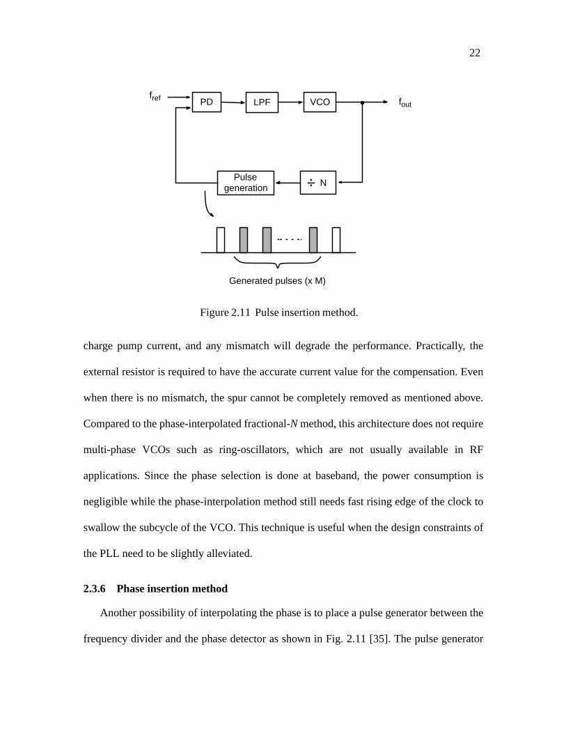
2.3.6 Phase insertion method
Another possibility of interpolating the phase is to place a pulse generator between the
frequency divider and the phase detector as shown in Fig. 2.11 [35]. The pulse generator
foutLPFfref PD
NPulse
generation
VCO
Generated pulses (x M)
Figure 2.11 Pulse insertion method.

23
insertsM new pulses between the frequency divider output pulses so that the frequency of
the pulse generator output becomesM + 1 times higher than that of the frequency divider
output. The VCO frequency fvco is given by
(2.5)
whereN is the division ratio of the frequency divider and the step size of this synthesizer is
fref/(M + 1). Therefore, the reference frequency can be madeM + 1 times higher than the
step size. As shown in Fig. 2.11, the pulse generator acts as a frequency multiplier. Like the
phase interpolation technique, the incorrect pulse position will degrade the spur
performance.
f vco Nf ref
M 1+--------------
,⋅=

24
CHAPTER 3
INTERPOLATIVE FREQUENCY DIVISION BY OVERSAMPLING
Oversampling data converters are widely used to achieve high dynamic range as the
power and the area of high-speed digital circuits become less significant with advanced
CMOS technology. Like a channel coding technique in digital communications, the
redundant output bits make the system robust against possible bit errors caused by analog
mismatches. Use of noise-shaped modulators in frequency synthesis also alleviates the
analog design constraints of the PLL and offers several advantages over the standard
approach.
3.1 Basic Concept
Fractional-N frequency synthesizers using∆−Σ modulators achieve fine frequency
resolution in such a way that the fractional division ratio is interpolated by an oversampling
∆−Σ modulator with a coarse integer divider [30]. In other words, the desired fractional
division ratio is similar to the dc input of an oversampling analog-to-digital converter
(ADC), and the integer divider is analogous to the one bit quantizer as shown in Fig. 3.1.
Since the second-order or higher modulators do not generate fixed tones, they are employed
to randomize the control input of the dual-modulus divider. In the ideal case, the resulting
system does not generate any spur, and the near-in phase noise due to modulation is shaped
to move into high frequencies. The∆−Σ modulation technique is similar to the random
jittering method [28], but it does not have a1/f2 phase noise spectrum due to its noise
shaping property.

25
Generally, the oversampling concept is valid only when the signal-to-noise ratio (SNR)
at baseband is considered. In other words, the noise power remains the same in the system
but the oversampling technique improves the SNR by filtering out the high-frequency noise
with the decimation filter. By having an integrator in the feedforward loop, the noise-
shaped oversampling modulator or the∆−Σ modulator improves the SNR more efficiently.
The∆−Σ modulators for the fractional-N synthesizer may not use the decimation filter to
suppress the high-frequency noise in the digital domain since the PLL with integer-N
dividers does not allow an intermediate level betweenN andN + 1. Therefore, the clock
frequency of the oversampling modulator must be same as the phase detector frequency in
order to not increase the quantization noise. However, the PLL acts as a low-pass filter to
the quantization noise, and the noise-shaped oversampling technique can be realized even
though the oversampling modulator is working at phase detector frequency. The effective
oversampling ratio, OSReff , can be defined by the ratio of the phase detector frequency fPD
to the PLL noise bandwidthfc, or
Figure 3.1 Basic concept of interpolated fractional division.
VCON/N+1
∆−Σmodulator
KN-1
N+1
1b quantizer
Oversampled output
P/FD1
N+1/4
0
...000100010001...

26
(3.1)
Narrowing the loop bandwidth increases the effective oversampling ratio, which results in
high in-band SNR. When high-order∆−Σ modulators are used, the PLL needs more poles
in the loop filter to suppress the quantization noise at high frequencies.
3.2 Modulator Architectures
For the∆−Σ modulators in fractional-N frequency synthesis, two major architectures
have been proposed in the literature [29], [30]. One is the single-stage high-order modula-
tor, and the other is the multi-stage cascaded modulator, which is often called the MASH
modulator. The advantages and disadvantages of each architecture will be discussed in this
section. The modulators with a multi-bit quantizer will be also discussed.
3.2.1 Single-stage high-order modulator
Figure 3.2 shows the simplified third-order modulator with a single-bit quantizer. The
noise transfer function (NTF) is given by
OSRef f
f PD
2 f c---------
.=
Figure 3.2 Single-stage high-order architecture.
XΣ
D
Σ DΣY
Σ Σ
D
Σ

27
(3.2)
whereN is the order of the modulator. Since the single-bit modulator generates only two-
level outputs, the dual-modulus divider can be directly used. It is also immune to the non-
linearity of the PLL by having a two-level quantizer. However, the single-bit modulator
suffers from the stability problem for high-order structures and limits the input range that
is to be less than the full-scale range of the quantizer for stable operation. Without design-
ing the NTF for that purpose, the practical use is limited to the second-order topology
unless the input range is substantially reduced [36], [37].
3.2.2 MASH modulator
The MASH modulator is designed by cascading the first-order modulators [38]. Due
to its inherent stable nature, the MASH architecture offers the maximum input range
almost equal to the full range of the quantizer. Without having feedback or feedforward
path, the design of the high-order MASH modulator is relatively easy to implement in the
pipeline architecture to increase the data throughput with low supply voltage [1], [2]. Fig-
ure 3.3 shows the third-order MASH modulator and the quantization noise is generated as
follows.
(3.3)
Note that the high-order MASH modulator has the high-order shaped quantization noise
by canceling the residual noise of the previous stage. The noise performance is identical to
Hn z( ) 1 z 1––( )N
,=
Q z( ) E0 E1 E2+ +=
E 1 z 1––( ) E 1 z 1––( )– E 1 z 1––( )2
+ E 1 z 1––( )2
– E 1 z 1––( )3
+ + +=
E 1 z 1––( )3
.=

28
that of the single-stage high-order topology in theory, but the noise-generation scheme is
slightly different.
The drawback of this architecture is that it requires a decimation filter with multi-bit
input in the ADC, or the multi-modulus divider in the synthesizer. Wide-spread output bit
pattern induces high-frequency jitter at the phase detector output, which gives more
stringent requirement on the phase detector design compared to the single-stage
architecture. Even though the MASH architecture offers inherent stability to any order over
all regions of operation, the performance will be limited by the noise smeared from the first-
stage modulator. When this point is reached, no gain in performance will be realized by
adding more stages to increase the overall modulator order [39]. An improved architecture
has been proposed by using a second-order modulator at the first stage in the cascade [40].
Figure 3.3 Cascaded (MASH) architecture.
ΣD
Σ D
ΣY
Σ
D
xi+ei-ei-1
xi-1-ei-2+ei-ei-1
XΣ DΣ
xi-ei-1

29
3.2.3 Multi-bit modulator
The oversampling ADC with a multi-bit quantizer provides high SNR for low
oversampling ratio by reducing the quantization noise itself [41]. By allowing larger dither
signal at the quantizer input, the stability problem and the nonlinearity effect are much
alleviated. However, imperfect matching of levels mainly due to the DAC nonlinearity
limits the overall performance. The use of the multi-bit modulator in frequency synthesizer
design has some different aspects, which will be discussed in next chapter.
3.3 Quantization Noise
The quantization noise effect of the∆−Σ modulator in frequency synthesis is well
analyzed in the literature [29], [30]. Assuming the uniform quantization error, the error
power is to be 1/12 where the minimum step size of the quantizer is set to 1 due to the
integer-divider quantization. This noise power is spread over a bandwidth of the phase
detector frequency fPD and the frequency fluctuation in thez-domainSv(z) with the NTF
Hn(z) is given by
(3.4)
Since the phase fluctuationSΦ(z) is the integration of the frequency fluctuation, it is
(3.5)
If SΦ(z) is a two-sided power spectral density (PSD), then the single-sided PSDL(z) is same
asSΦ(z). When the NTF in Equation (3.3) is assumed, theL(z) is given by
Sv z( ) Hn z( ) f PD2 1
12 f PD----------------
Hn z( ) 2 f PD
12---------
.⋅=⋅=
SΦ z( ) 2π1 z 1–– f PD
----------------------------î 2 Hn z( ) 2
f PD
12------------------------------
.⋅=
30
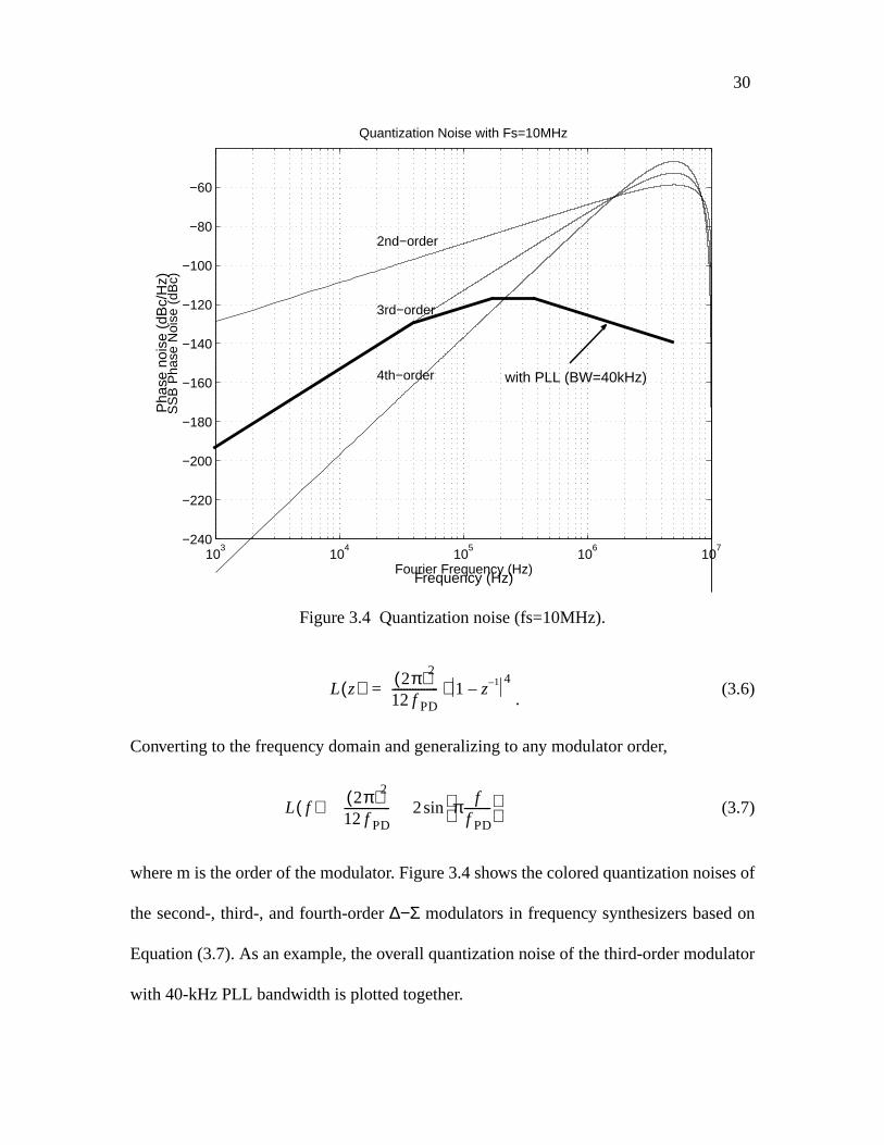
(3.6)
Converting to the frequency domain and generalizing to any modulator order,
(3.7)
where m is the order of the modulator. Figure 3.4 shows the colored quantization noises of
the second-, third-, and fourth-order∆−Σ modulators in frequency synthesizers based on
Equation (3.7). As an example, the overall quantization noise of the third-order modulator
with 40-kHz PLL bandwidth is plotted together.
L z( ) 2π( )2
12 f PD---------------- 1 z 1––
4
.⋅=
Figure 3.4 Quantization noise (fs=10MHz).
103
104
105
106
107
−240
−220
−200
−180
−160
−140
−120
−100
−80
−60
Quantization Noise with Fs=10MHz
Fourier Frequency (Hz)
SS
B P
hase
Noi
se (
dBc)
2nd−order
3rd−order
4th−order with PLL (BW=40kHz)
Frequency (Hz)
Pha
se n
oise
(dB
c/H
z)
L f( ) 2π( )2
12 f PD---------------- 2 π f
f PD---------
sinî 2 m 1–( )
,⋅=

31
3.4 Dynamic Range Considerations
Numerous theories have been developed in oversampling ADC or DAC modulators.
Most issues in the∆−Σ modulator design for fractional-N synthesizers are similar to those
of the oversampling data converters. The main difference is that the oversampling
modulators for the fractional-N synthesizers are to be analyzed in the frequency or in the
phase domain, while they are considered in the voltage domain for the data converters.
By interpreting the well-known results of the oversampling ADC into the frequency
domain, the generalized equation regarding the loop bandwidth requirement can be derived
in terms of the in-band phase noise, the phase detector frequency, and the order of the∆−Σ
modulator.
If the in-band phase noise ofAn (rad2/Hz) of the frequency synthesizer is assumed to
be limited within the noise bandwidth offc (Hz) as shown in Fig. 3.5, the integrated fre-
quency noise∆fn (rms Hz) withinfc is approximately [42]
(3.8)
wherefc >> fo assumed. Because the quantizer level in the frequency domain is equivalent
to fPD with the frequency noise of∆fn as illustrated in Fig. 3.5, the dynamic range of the
Lth-order∆−Σ modulator should meet the following condition [41].
(3.9)
∆ f n 2 An f2⋅( ) fd
f O
f C
∫=
23---An f c
32---
,⋅≅
32--- 2L 1+
π2L---------------- OSRef f( )2L 1+ f PD
∆ f n---------
2
,>⋅ ⋅

32
where OSReff is defined in Equation (3.1). Therefore, from Equations (3.1), (3.8), and
(3.9), we obtain
(3.10)
An integrated phase errorθrms [rms rad] is an important factor for synthesizers in digital
communications, and it is given by
(3.11)
From Equations (3.10) and (3.11), an approximate upper bound of the bandwidth is
obtained, or
(3.12)
Equation (3.12) gives an advantage of using an integrated phase error as a parameter,
which is not included in the previous results [29], [30]. For example, when the phase
Figure 3.5 Dynamic range consideration in oversampled fractional division.
-fPD/2
+fPD/2
Required dynamic range > (fPD/∆fn)2
∆fn
Quantizer
Interpolated frequency
fcf [Hz]
fBW
In-band noise
10 log (An)
Phase noise[dBc/Hz]
Synthesizer phase noise
f c AnL 0.5+
2π( )2L-----------------⋅
12L 2–---------------
f PD
2L 1–2L 2–---------------
.⋅<
θrms 2An f c⋅ .=
f c
θrms
2----------
2 L 0.5+
2π( )2L-----------------⋅
12L 1–----------------
f PD.
⋅<

33
detector frequency is 8 MHz, the upper bound of the bandwidth with the third-order∆−Σ
modulator to meet less than 1o-rms phase error is 195 kHz. Practically, the required loop
bandwidth is narrower than that by Equation (3.12) since the quantization noise of the 3rd-
order modulator is tapered off after the 4th pole of the PLL. In this work, the loop band-
width is set to 40 kHz with the 3rd pole placed at 160 kHz.
3.5 Idle Tones
It is known that even high-order∆−Σ modulators generate idle tones with some dc
input. The tonal behavior of the modulator is easily observed especially when the ratio of
the dc input offset to the full-scale input level is a rational number. The tones occur in the
output spectrum of the modulator at frequencies given by [43],
(3.13)
and
(3.14)
where Aoffset is the input dc offset level andAquant is the full-scale input level of the
quantizer. Even though the tone atftone2 does not occur within the band, it generates an in-
band tone from the two strong signals near half the sampling frequency [44]. In MASH
architectures, each modulator should have its own independent dither to provide the most
decorrelation of the quantization errors [45]. For example in an analog implementation,
there will be imperfect matching between stages, which will make the overall outcome
f tone1
Aof fset
Aquant--------------- m f s
,⋅=
f tone2 1Aof fset
Aquant---------------–
m f s ,⋅=

34
more prone to residual tones of the previous stage [46]. Also, each stage is potentially
capable of coupling higher frequency tones nearfs/2 into other stages.
In order to eliminate any audible artifacts of the repetition of the sequence, it is wise to
choose a sequence length of the modulator that spans at least several seconds in real-time
implementation. A typical way to have the dithering for the digital modulator is to set the
least-significant bit (LSB) to high all the time [30]. That is, the offset frequency equivalent
to the minimum resolution frequency is added to the desired frequency to decorrelate the
quantization error since inputs which excite only bits near the most-significant bit (MSB)
position result in a limit cycle of short duration and insufficient randomness. With the use
of 24-bit sequence, one LSB corresponds to less than 1-Hz frequency error, or less than
0.001 ppm for 1-GHz output. The fractional spur in the frequency synthesizer also stems
from other sources, which will be discussed later.
3.6 Stability
Being cascaded by first-order modulators, the MASH modulators are guaranteed to be
stable regardless of the number of order. For that reason, the MASH topology is mostly
employed in synthesizer applications. For high-order single-stage topology, building stable
system is the first step to be taken care of in the modulator design. There are two kinds of
stability considerations. One is small-signal (linear) stability and the other is large-signal
(nonlinear) stability. For the small-signal stability, the loop is stable as long as all the poles
are located inside the unit circle in thez-domain, which can be easily achieved by choosing
the appropriate coefficient for the NTF.

35
However, the modulator may not work well even with the proper pole location if there
is any chance for the accumulator or the integrator to be saturated due to nonlinear effects
of the feedback loop. In fact, it happens for most single-bit high-order modulators that do
not have the well-defined small-signal gain for the two-level quantizer. One possible way
to avoid this kind of problem is to reduce the maximum input signal range. Unfortunately,
reducing the input range as done in data converters is not allowed in most synthesizer
applications since the full range of the quantizer should be used to avoid any dead band, as
will be discussed in Chapter 4.
36
CHAPTER 4
HIGH-ORDER ∆−Σ MODULATOR WITH MULTI-LEVEL QUANTIZER
High-order∆−Σ modulators effectively shape the quantization noise, but the stability
problem often limits the performance. The multi-bit high-order modulator is considered in
this work to enhance the overall synthesizer performance. In following sections, the use of
a multi-bit oversampling modulator in frequency synthesis is introduced, and its
performance is discussed.
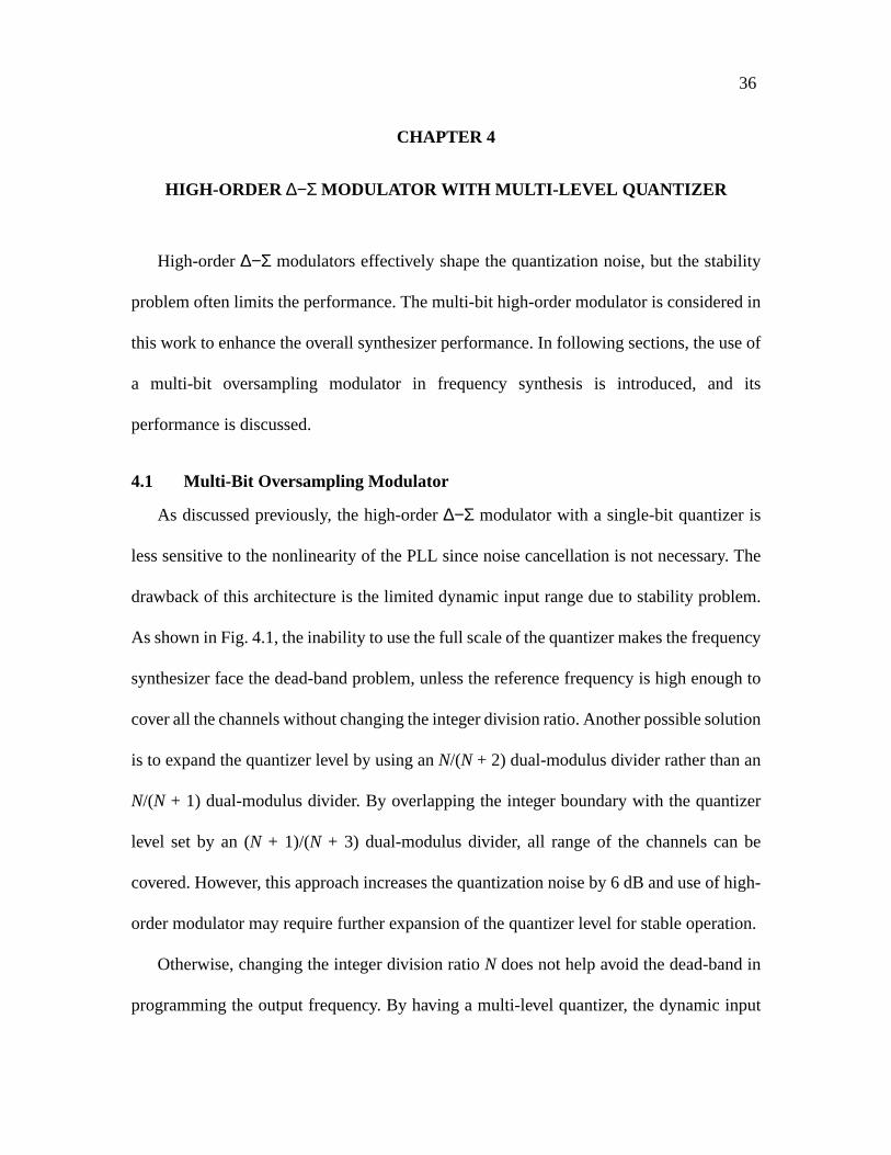
4.1 Multi-Bit Oversampling Modulator
As discussed previously, the high-order∆−Σ modulator with a single-bit quantizer is
less sensitive to the nonlinearity of the PLL since noise cancellation is not necessary. The
drawback of this architecture is the limited dynamic input range due to stability problem.
As shown in Fig. 4.1, the inability to use the full scale of the quantizer makes the frequency
synthesizer face the dead-band problem, unless the reference frequency is high enough to
cover all the channels without changing the integer division ratio. Another possible solution
is to expand the quantizer level by using anN/(N + 2) dual-modulus divider rather than an
N/(N + 1) dual-modulus divider. By overlapping the integer boundary with the quantizer
level set by an (N + 1)/(N + 3) dual-modulus divider, all range of the channels can be
covered. However, this approach increases the quantization noise by 6 dB and use of high-
order modulator may require further expansion of the quantizer level for stable operation.
Otherwise, changing the integer division ratioN does not help avoid the dead-band in
programming the output frequency. By having a multi-level quantizer, the dynamic input

37
range problem can be solved. The eight-level quantizer in Fig. 4.1 expands the active
division range from N, N + 1 to N – 3,N – 2, ...,N + 3, N + 4 without increasing the
minimum quantizer level. Therefore, the multi-bit high-order modulator can be easily
designed to be stable over all interpolated range betweenN andN + 1, which is about 12%
of the full range of the quantizer. The extended input range with the multi-level quantizer
helps reduce the nonideal effects at the band edges.
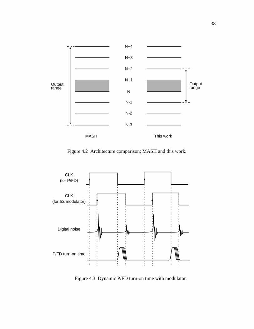
Compared to the MASH modulator, the multi-bit high-order modulator has less high-
frequency noise at the phase detector output. Although the MASH topology with the same
order can shape the in-band noise more sharply, it produces an output bit pattern spread
more widely than the proposed noise shaper does as shown in Fig. 4.2. Different from the
integer-N synthesizer, the fractional-N synthesizer with the∆−Σ modulator makes the
charge pump have the dynamic turn-on time after phase-locked as illustrated in Fig. 4.3.
N
N+1
N+2
N+3
N+4
N-1
N-2
N-3
Inputrange
Inputrange
Single-bit This work
Figure 4.1 Architecture comparison; single-bit and this work.
38
N
N+1
N+2
N+3
N+4
N-1
N-2
N-3
Outputrange
MASH This work
Outputrange
Figure 4.2 Architecture comparison; MASH and this work.
P/FD turn-on time
CLK
Digital noise
(for ∆Σ modulator)
CLK(for P/FD)
Figure 4.3 Dynamic P/FD turn-on time with modulator.

39
Widely spread output bit pattern makes the synthesizer more sensitive to the substrate noise
coupling as the modulated turn-on time of the charge pump in the locked condition
increases. The architecture comparison is summarized in Table 4.1.
4.2 Design of Single-Stage High-Order ∆−Σ Modulator
The ∆−Σ modulator design for the frequency synthesizer has some different aspects.
Since it consists of digital blocks having digital input and output, the coefficients of the
modulator can be controlled well. However, the modulator design for the frequency
synthesizer still faces the analog matching problem since the digital information is
transformed into the phase error in the analog domain when combined with the PLL. The
issues in the design of the digital modulator for frequency synthesizers will be discussed in
the following sections.
Table 4.1 Modulator architecture comparison.
Single-bit This work
Stability
Input range
Output range
Quantizationnoise (in-band)*
Quantizationnoise (out-band)*
Idle tone
MASH
Possibly unstable Stable Stable
< 100%of quantizer
almost 100%of quantizer
> 100%of quantizer
at most 2 levels almost 8 levels at most 4 levels
Poor Good Fair
PoorGood Good
Fair Fair Good
*Butterworth design is assumed except for MASH.

40
4.2.1 Choice of NTF
Different from the MASH modulator, the single-stage high-order∆−Σ modulator needs
careful NTF design for stable operation. Three conditions should be met for the NTF to be
valid [39]. The first condition is satisfying the causality condition to prevent the delay-free
loop that cannot be implemented in the hardware. Only the quantization error incurred in
the past is allowed to form the current input to the quantizer. This requirement can be met
by setting the leading coefficients of the numerator and the denominator polynomials of
Hn(z) to 1, or
(4.1)
The second condition is the small-signal stability. The poles of the NTF need to be within
the unit circle in thez-domain. Since the digital modulator accurately controls the
coefficients, it can be easily met. However, the location of the poles must be checked
carefully when the coefficient adjustment is done to simplify the hardware. The third
condition is the large-signal or nonlinear stability, which is difficult to predict. Empirical
study of the nonlinear stability shows that the passband gain should be limited [47].
Butterworth design is a good choice to have the flat frequency response over passband and
the passband gain can be set by controlling the cutoff frequency. Note that to meet both the
causality condition and the passband gain rule, there are no degree of freedom [39]. In other
words, once a Butterworth filter is chosen, there is one and only one choice of cutoff
frequency that meets both conditions. The Butterworth filter for the NTF is often a good
choice and is commonly used in commercial products. One reason for this is that the poles
are relatively low-Q, and therefore, the∆−Σ modulator tends to be less susceptible to
Hn ∞( ) 1 .=
41
oscillations. It also reduces the high-frequency noise energy resulting in low-spread output
bit pattern, which is useful in frequency synthesizer design as discussed previously.
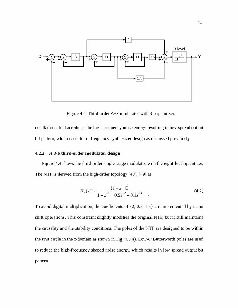
4.2.2 A 3-b third-order modulator design
Figure 4.4 shows the third-order single-stage modulator with the eight-level quantizer.
The NTF is derived from the high-order topology [48], [49] as
(4.2)
To avoid digital multiplication, the coefficients of 2, 0.5, 1.5 are implemented by using
shift operations. This constraint slightly modifies the original NTF, but it still maintains
the causality and the stability conditions. The poles of the NTF are designed to be within
the unit circle in thez-domain as shown in Fig. 4.5(a). Low-Q Butterworth poles are used
to reduce the high-frequency shaped noise energy, which results in low spread output bit
pattern.
X Σ D Σ DΣ
2
YΣ
1.5
Σ D 0.5
8-level
Figure 4.4 Third-order∆−Σ modulator with 3-b quantizer.
Hn z( ) 1 z1––( )
3
1 z1–– 0.5z
2– 0.1z3––+
---------------------------------------------------------.
≈

42
Figure 4.5 Proposed modulator: (a) pole-zero plot, and (b) noise transfer function.
(a)
(b)
−1 −0.5 0 0.5 1
−1
−0.8
−0.6
−0.4
−0.2
0
0.2
0.4
0.6
0.8
1
Real part
Imag
inar
y pa
rt
3rd−Order Single−Stage MF Loop
3
x
x
x
0 0.05 0.1 0.15 0.2 0.25 0.3 0.35 0.4 0.45 0.50
1
2
3
4
5
6
7
8Noise Transfer Function
Normalized Frequency
|Hn(
z)|
MB
MASH

43
For high-order modulators, it has been shown that as the number of quantizer levels
increases, the maximum passband gain of the NTF can be increased without causing any
nonlinear stability problem [50], [51]. As the maximum passband gain of the NTF
increases, the corresponding corner frequency increases. For example, if the input range is
set to about 80% of the quantizer, the maximum passband gain of the NTF can be set to 2.5
for a 2-b quantizer, 3.5 for a 3-b quantizer, and 5.0 for a 4-b quantizer. The corresponding
corner frequencies of the NTF are 0.13fs, 0.19fs, and 0.24fs, respectively. This implies that
quantization noise of the third-order modulator can be further suppressed by 16 dB with a
2-b quantizer, 22 dB with a 3-b quantizer, and 25 dB with a 4-b quantizer [50]. As shown
in Fig. 4.5(b), the NTF of the proposed modulator has the passband gain of 3.1 and the
corner frequency of 0.18 fs for the clock frequency fs. Note that the high corner frequency
is preferred for in-band noise suppression, but it increases the high-frequency noise energy.
Figure 4.6 shows the time-domain simulation of the division ratio for 1000 sequences
generated by the 3-b third-order modulator. The simulation is done with the behavioral
model of the gate-level modulator in PSPICE. The fractional division ratio is set to
1/4+1/27 and the 16th bit is used for dithering. That is, the actual fractional division ratio
is 1/4+1/27+1/216. Note that this interpolator uses mostly the closely spaced division val-
ues ofN, N – 1, andN + 1 to generate the fractional value. The fast Fourier transform
(FFT) of the modulator output is shown in Fig. 4.7. As predicted from the NTF in Fig.
4.5(b), the quantization noise has the flat passband gain with the corner frequency of less
than 0.2fs.

44
0 100 200 300 400 500 600 700 800 900 1000−3
−2
−1
0
1
2
3
4
Sequence
Mul
ti−m
odul
us d
ivis
ion
3rd−Order Delta−Sigma (MF) with .f = 1/2^7 + 1/2^16
Figure 4.6 3-b third-order modulator output stream forN + 1/4 + 1/27 divisionwith dithering in time domain.
10−3
10−2
10−1
100
−100
−80
−60
−40
−20
0
20
40
60
Normalized Frequency
Qan
tizat
ion
Noi
se
3rd−Order Delta−Sigma (MF) for .f = 1/2^7 + 1/2^16
Figure 4.7 FFT of 3-b third-order modulator output forN + 1/4 + 1/27 divisionwith dithering.

45
The discrete Fourier transform does not provide thetrue power spectrum, particularly
when the signal is aperiodic or random. To see the randomness of the output sequence, the
autocorrelation estimate is used and it is given by [52]
(4.3)
Figure 4.8 shows the autocorrelation of 2000 output samples with the fractional division
ratio of 1/4 + 1/27 + 1/216. For the random signal, the autocorrelation function should be
zero except forRx(0). A high peak-to-rms power ratio of pattern noise sequence is harmful
since it may produce an audible tones in the baseband for some dc input levels [45]. It is
known that the high-order noise shaping with the multi-bit quantization makes the dither-
ing more efficient.
RX n( ) 1N---- X m( ) X m n+( ) .⋅
m 0=
N 1–
∑=
0 200 400 600 800 1000 1200 1400 1600 1800 2000−0.2
0
0.2
0.4
0.6
0.8
Sequences
Nor
mal
ized
Aut
o−C
orre
latio
n
3rd−Order Delta−Sigma (MF) with .f = 1/2^7 + 1/2^16
Figure 4.8 Autocorrelation of 2000 samples withN + 1/27 + 1/216division.

46
4.3 Phase Detector Linearity
In general, the multi-bit modulators have no linearity problem, but when it is com-
bined with the PLL, the nonlinearity of the phase detector is a concern. Figure 4.9 shows
the similarity between the multi-bit oversampling ADC and the frequency synthesizer
having the multi-bit modulator. The frequency synthesizer has the multi-level feedback
inputs in the time domain generated by the modulated multi-modulator divider, whereas
the multi-bit ADC has the multi-level feedback inputs in the voltage domain generated by
the multi-bit DAC. It is well known that the multi-bit DAC limits the in-band noise perfor-
mance as well as the spurious tones performance. Therefore, the same behavior by the
multi-modulus divider with the modulator may be intuitively expected. However, the
multi-modulus divider and the modulator conveys the information in the digital domain
without having the linearity issue. The phase detector converts the digital quantity into the
analog quantity by generating the multi-phase errors, and the phase detector nonlinearity
Figure 4.9 Multi-bit oversampling: (a) ADC, and (b) frequency synthesizer.
8-levelΣ
fout
N/N+1 ,.., /N+7
∆−Σmodulator
3
LPF VCOfin
ΣDout
DAC
LPFVin
8-leveloutput
(a) (b)
3
8-leveloutput

47
is considered the main contributor for the nonideal effects of the∆−Σ modulated fre-
quency synthesizer.
Periodic tones are visible in simulations when the division ratio is close to the frac-
tional-band edges. Figure 4.10 shows the simulation results for the division ratio ofN +
1/27 with 0.1% and 1% mismatches. For simplicity, the simulations are done in the fre-
quency domain rather than in the phase domain to show the nonlinearity effect in the
open-loop condition. The results show that the nonlinearity limits the spurious tones and
the in-band phase noise. In the simulation, the third-order modulator has a 6-dB lower
spur level than the second-order modulator. Therefore, higher-order modulators are
needed not only for lower in-band noise but also for lower spur levels.

48
Figure 4.10 FFT of 3-b third-order modulator dithered output forN + 1/27
division: (a) with 0.1% nonlinearity, and (b) with 1% nonlinearity.
(a)
(b)
10−3
10−2
10−1
100
−100
−80
−60
−40
−20
0
20
40
603rd−Order DS (MF) for .f = 1/2^7 + 1/2^16 with 0.1% Nonlinearity
Normalized Frequency
Qan
tizat
ion
Noi
se
10−3
10−2
10−1
100
−100
−80
−60
−40
−20
0
20
40
603rd−Order DS (MF) for .f = 1/2^7 + 1/2^16 with 1% Nonlinearity
Normalized Frequency
Qan
tizat
ion
Noi
se

49
CHAPTER 5
DESIGN CONSIDERATIONS FOR HIGH SPECTRAL PURITY
A frequency synthesizer generates a stable signal, which is ideally a single tone in the
frequency domain. In reality, the signal is not pure at all, and the unwanted information is
added in two ways: random or deterministic [42]. Phase noise and spurious tones often limit
the overall synthesizer performance. The noise from the synthesizer without the VCO and
the spurious tones can be reduced by narrowing the PLL bandwidth, but the narrow-band
PLL suffers from long settling time. It also put stringent requirement for the VCO noise
performance. Therefore, there is a trade-off to determine the synthesizer performance in
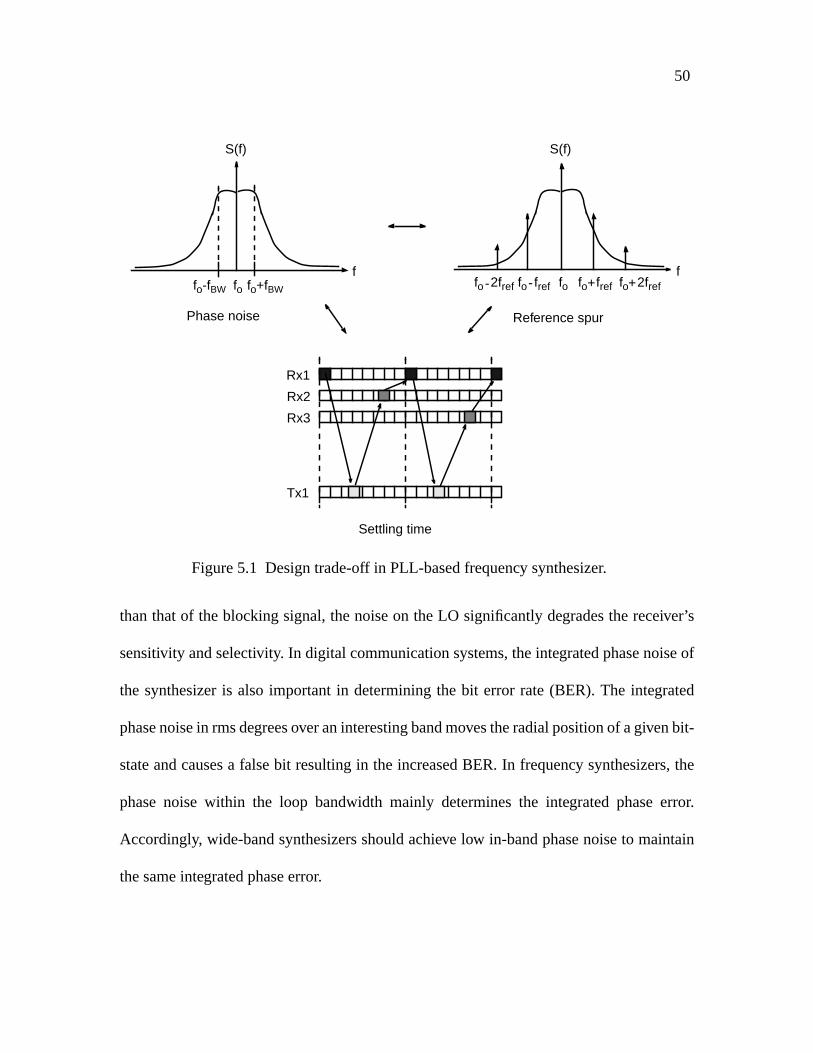
terms of the phase noise, the spurious tone, and the settling time as illustrated in Fig. 5.1.
In this chapter, the system-level design of frequency synthesizers for high spectral purity
will be discussed.
5.1 Phase Noise
Phase noise is the randomness of the frequency instability. In RF frequency
synthesizers, the phase noise is one of the most important specifications. Figure 5.2(a)
shows the example of the blocking-signal specification for GSM receivers [53]. The RF
signal is mixed with a local oscillator (LO) signal down to an intermediate frequency (IF).
Although the receiver’s IF filtering may be sufficient to remove the interfering signal’s main
mixing product, the desired signal’s mixing product is masked by the downconverted phase
noise of the LO. Since the power of the desired signal as low as -102 dBm is much weaker
50
than that of the blocking signal, the noise on the LO significantly degrades the receiver’s
sensitivity and selectivity. In digital communication systems, the integrated phase noise of
the synthesizer is also important in determining the bit error rate (BER). The integrated
phase noise in rms degrees over an interesting band moves the radial position of a given bit-
state and causes a false bit resulting in the increased BER. In frequency synthesizers, the
phase noise within the loop bandwidth mainly determines the integrated phase error.
Accordingly, wide-band synthesizers should achieve low in-band phase noise to maintain
the same integrated phase error.
Figure 5.1 Design trade-off in PLL-based frequency synthesizer.
fo+fBWfof
S(f)
fo
S(f)
ffo fref+ fo 2fref+fo 2fref- fo fref-
Rx1
Rx2
Rx3
Tx1
Phase noise Reference spur
Settling time
fo-fBW

51
5.1.1 Phase noise generation principle
By interpreting the noise as a normalized signal within 1-Hz bandwidth, the phase noise
can be analyzed by employing narrow-band FM theory [54]–[56]. The oscillator outputS(t)
can be expressed by
(5.1)
whereV(t) describes the amplitude variation as a function of time, andθ(t) the phase
variation or phase noise. A well-designed, high-quality oscillator is amplitude-stable, and
V(t) can be considered constant. For a constant amplitude signal, all oscillator noise is due
to θ(t). A carrier signal of amplitudeV and frequency fo, which is frequency-modulated by
a sine wave of frequency fm, can be represented by
Figure 5.2 Blocking signal in GSM.
Desiredsignal
fo-6
00kH
z
fo-1
.6M
Hz
fo-3
MH
z
fo+
600k
Hz
fo+
1.6M
Hz
fo+
3MH
z
fo
f
-23
-33
-43
-102
-23
-33
-43In
terf
erin
g si
gnal
s (d
Bm
)
S t( ) V t( ) ωot θ t( )+[ ] ,cos=

52
(5.2)
where∆f is the peak frequency deviation andθp (=∆f/fm) is the peak phase deviation – often
referred to as themodulation index m. Equation (5.2) can be expanded as
(5.3)
If the peak phase deviation is much less than ( ), then the signalS(t) is approximately
equal to
(5.4)
That is, when the peak phase deviation is small, the phase deviation results in frequency
components on each side of the carrier of amplitude ofθp/2. This frequency distribution of
a narrowband FM signal is useful for interpreting an oscillator’s power spectral density as
being due to phase noise. The phase noise in a 1-Hz bandwidth has a noise power-to-power
ratio of
(5.5)
The total noise is the noise in both sidebands and will be denoted bySθ. That is,
(5.6)
S t( ) V ωot∆ff m------ ωmtsin+
,
cos=
S t( ) V ωot( )cos θp ωmtsin( ) ωot( ) θp ωmtsin( )sinsin–cos[ ] .=
θp 1«
S t( ) V ωot( ) ωot( ) θp ωmtsin( )sin–cos[ ]=
V ωot( )θp
2----- ωo ωm+( )t ωo ωm–( )tcos–cos[ ]–cos
î
=.
L f m( )V n
V------
2 θp
2
4--------
θrms2
2-------------
.== =
Sθ 2θrms
2
2------------- θrms
22L f m( )
.===

53
5.1.2 Integrated phase noise
As mentioned previously, the integrated phase fluctuations in rms degrees can be useful
for analyzing system performance in digital communication systems. Integrated noise data
over any bandwidth of interest is easily obtained from the spectral density functions.
Integrated frequency noise (rms Hz), commonly calledresidual FM, can be found by
(5.7)
Integrated phase noise (rms rad) is determined similarly,
(5.8)
For example, the integrated phase noise of -38 dBc corresponds to 0.0178 (rms rad), or 1
(rms deg).
5.1.3 Effect of frequency division and multiplication on phase noise
It is interesting to know the effect of frequency division and multiplication on phase
noise [54]. Equation (5.9) states that the instantaneous phaseθi(t) of a carrier frequency
modulated by a sine wave of frequency fm is given by
(5.9)
Instantaneous frequency is defined as the time rate of change of phase, or
(5.10)
∆ f n 2L f m( ) f m2
f mda
b
∫ .=
∆θn 2L f m( ) f mda
b
∫ .=
θi t( ) ωot∆ff m------+ ωmt
.sin=
ωdθi
dt-------- ωo
∆ff m------ωm ωmt ωo ∆ω
.+≤cos+= =

54
If this signal is passed through a frequency divider that divides the frequency by N, the
output phaseθo(t) will be given by
(5.11)
The divider reduces the carrier frequency by N, but does not change the frequency of the
modulating signal. The peak phase deviation is reduced by the divide ratio ofN. Since it
was shown in Equation (5.5) that the ratio of the noise power to carrier power isθp2/4, the
frequency division byN reduces the noise power byN2.
5.1.4 Noise generation in frequency synthesizers
In synthesizer design, it is important to identify the phase noise contribution from each
source. Overall phase noise is determined mainly by three noise sources, the VCO, the PLL
including a frequency divider and a phase detector, and the reference source. The noise
contributions of each source for the given PLL open-loop gain are plotted in Fig. 5.3. The
VCO noise that has the slope of -30 dB/dec below the frequency f1 and the slope of -20
dB/dec above f1 is suppressed by the open-loop gain G(f) that has the slope of -20 dB/dec
from the zero frequency fz of the loop filter to the unity-gain bandwidthfunity, and the slope
of -40 dB/dec below fz . Since the PLL does not provide any suppression for the out-of-band
VCO noise, the VCO noise often determines the out-of-band phase noise in standard
integer-N synthesizers. The PLL noise by the frequency divider and the phase detector as
well as the reference source noise determines the in-band phase noise since the PLL
suppresses only out-of-band noise. Also, their noise contribution at the synthesizer output
θo t( )ωot
N-------- ∆f
Nf m----------+ ωmt
.sin=

55
Figure 5.3 Noise sources in frequency synthesizer.
G(f)
f
-40dB/dec
-20dB/dec
-40dB/dec
-60dB/dec
fz fp1 fp2funity
L(f)
f
f1
Overall
PLL
VCO
Reference

56
is multiplied by the division ratio as explained in the previous section. Since the in-band
noise is a dominant factor for the integrated phase error, the low-noise design of the phase
detector and the frequency divider is important assuming that a stable external reference
source is available. Therefore, optimizing the loop filter is important as each noise source
is sensitive to the open-loop gain of the PLL. As shown in Fig. 5.3, the open loop gain needs
to be carefully designed to have the overall output noise meet the system specification.
Different from integer-N synthesizers, the∆−Σ fractional-N synthesizers have another
noise source, or the∆−Σ modulator. It can possibly affect both in-band noise and out-of-
band noise, depending on the design. The in-band noise may be limited by the modulator
due to poor phase detector nonlinearity rather than by the PLL noise or by the reference
source, and the out-of-band noise can be possibly determined by the residual quantization
noise of the modulator rather than the VCO noise, which will be discussed later.
5.2 Spurious Tones
While the phase noise represents the randomness of the frequency stability, the spurious
tone is set by the deterministic behavior. Since the spur generation is considered the
systematic offset in the PLL, it is relatively easy to improve the spur performance up to
certain level compared to improving the phase noise performance. The open-loop gain
determines the spur performance at the system-level design, and the phase detector
including the charge pump mainly limits the performance at the circuit-level design.
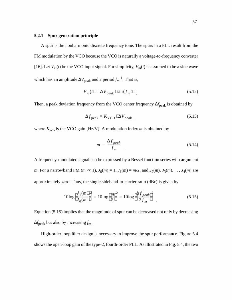
57
5.2.1 Spur generation principle
A spur is the nonharmonic discrete frequency tone. The spurs in a PLL result from the
FM modulation by the VCO because the VCO is naturally a voltage-to-frequency converter
[16]. LetVm(t) be the VCO input signal. For simplicity, Vm(t) is assumed to be a sine wave
which has an amplitude∆Vpeak and a periodfm-1. That is,
(5.12)
Then, a peak deviation frequency from the VCO center frequency ∆fpeak is obtained by
(5.13)
whereKvco is the VCO gain [Hz/V]. A modulation index m is obtained by
(5.14)
A frequency-modulated signal can be expressed by a Bessel function series with argument
m. For a narrowband FM (m << 1),J0(m) = 1,J1(m) = m/2, andJ2(m), J3(m), ... ,J4(m) are
approximately zero. Thus, the single sideband-to-carrier ratio (dBc) is given by
(5.15)
Equation (5.15) implies that the magnitude of spur can be decreased not only by decreasing
∆fpeak but also by increasingfm.
High-order loop filter design is necessary to improve the spur performance. Figure 5.4
shows the open-loop gain of the type-2, fourth-order PLL. As illustrated in Fig. 5.4, the two
V m t( ) ∆V peak f mt( ) .sin⋅=
∆ f peak KVCO ∆V peak ,⋅=
m∆ f peak
f m-----------------
.=
10J1 m( )J0 m( )---------------
210
m2----
210
∆ f peak
2 f m-----------------
2
.log=log=log

58
out-of-band poles atfp1 andfp2 provides additional spur suppression given by
(5.16)
When the spur level is given by the device, the only way to reduce the spur in integer-N
synthesizers is to have the narrower loop bandwidth or to have a higher-order loop filter
with the degraded phase margin resulting in longer settling time.
5.2.2 Spur generation in frequency synthesizers
A charge pump combined with the digital P/FD is widely used in modern synthesizer
ICs. Having a neutral state, the ideal charge pump provides the infinite dc gain without
Figure 5.4 Reference spur suppression by loop filter.
Additional spur suppressionby out-of-band poles
fz
fp1 fp2 fref
funity
G(f)
f
-40dB/dec
-20dB/dec
-40dB/dec
-60dB/dec
∆Pspur 20=f ref
f p1---------
20f ref
f p2---------
.
log+log

59
using an active loop filter. In other words, the type-2 PLL is possible with the passive filter
and the zero static phase error is achieved. It also provides the unbounded pull-in range for
second-order and higher-order PLLs if not limited by the VCO input range [57]. The charge
pump, however, is sensitive to any nonideal effects of the PLL since the timing information
is converted to an analogue quantity in voltage at the output of the charge pump. One of the
practical design issues in PLLs is the unbalanced large-signal operation caused by the
charge pump [58]. It makes the charge pump the dominant block that determines the level
of the unwanted FM modulation causing the reference spur.
5.2.2.1 Leakage current
One source of the reference spur is the leakage current caused by the charge pump itself,
by the on-chip varactor, or by any leakage in the board. The leakage current as high as 1 nA
can be easily present in submicron CMOS. The phase offset due to the leakage current is
usually negligible in digital clock generation, but the reference spur by the leakage current
is possibly substantial in frequency synthesizers as shown in Fig. 5.5. The phase offsetφε
(rad) due to the leakage currentIleak with the charge pump currentIcp is given by
(5.17)
The sideband due to the phase offset can be predicted using the narrow-band FM
modulation [16]. The amount of the reference spurPspur (dBc) in the third-order PLL is
approximately given by
φε 2πI leak
Icp----------
.⋅=

60
(5.18)
where R is the resistor in the loop filter, KVCO is the VCO gain, fref is the reference
frequency for the P/FD, andfp1 is the frequency of the pole in the loop filter. When the loop
is assumed to be overdamped, the loop bandwidthfBW with the division ratio N is
approximated by
(5.19)
Then, Equation (5.18) becomes
(5.20)
For example, if we assume thatfref= 200 kHz,fBW = 20 kHz,fout= 2 GHz (i.e,N = 10 000),
fp1 = 80 kHz,Icp= 1 mA, andIleak= 1 nA, the reference spur will be
fref
fdiv
Ileak
Figure 5.5 Phase offset due to leakage current.
Icp
φε
Pspur 202
IcpR
2π----------- φε KVCO⋅ ⋅ ⋅
2 f ref⋅-----------------------------------------------
20f ref
f P1---------
,
log–log=
f BW
Icp R KVCO⋅ ⋅2π N⋅
----------------------------------.
≅
Pspur 20f BW
f ref----------- N φε⋅ ⋅
20f ref
f P1---------
.
log–log=

61
(5.21)
If the spur level is not enough to meet the requirement, the loop bandwidth should be further
narrowed, or the charge pump current should be increased. Note that reducing the division
ratio by increasing the reference frequency is very helpful to improve the spur performance.
5.2.2.2 Mismatches in charge pump
Another consideration is the mismatch in the charge pump. Since CMOS charge pumps
usually have UP and DOWN switches with PMOS and NMOS, respectively, the current
mismatch and the switching time mismatch occur in dumping the charge to the loop filter
by UP and DOWN operations. The circuit needs to be optimized to minimize those effects.
When the mismatch is given in the charge pump, it is important to reduce the turn-on time
of the P/FD that is equivalent to the minimum pulse width of the outputs which is necessary
to remove the dead-zone. The phase offsetφε due to the current mismatch can be estimated
as illustrated in Fig. 5.6. Let the turn-on time of the P/FD, the reference clock period, and
the current mismatch of the charge pump denoted by∆ton, Tref, and∆i, respectively. The
amount of the phase offset is given by
(5.22)
Pspur 2020 kHz200 kHz--------------------- 10 000× 2π1 nA
1 mA--------------
× 20
200 kHz80 kHz---------------------
log–log=
52 dBc .–=
φε 2π∆ton
T ref---------- I ∆i+
I--------------- 1–
⋅ ⋅=
2π∆ton
T ref----------
∆iI
-----,
⋅ ⋅=

62
where∆i > 0 is assumed. Then, the spur level can be also derived similarly from Equations
(5.20) and (5.22). For the turn-on time of 10 ns in the P/FD and the same condition given
for Equation (5.21), the mismatch of 0.1% gives the amount of spur determined by
(5.23)
This shows how important to design the P/FD and the charge pump with the minimum turn-
on time as well as with the minimum mismatches. The minimum turn-on time is also
important to reduce the noise contribution of the charge pump current to the PLL. Since the
minimum turn-on time in the P/FD depends on the output loading by the charge pump and
fref
fdiv
UP
Effectiveoutput
DW
Locked with phase offset
(a) Iup = Idw
Locked without phase offset
(b) Iup > Idw
Figure 5.6 Phase offset due to charge pump mismatch.
Pspur 2020 kHz200 kHz--------------------- 10000× 2π 10 ns
5 µs------------- 0.001××
× 20
200 kHz80 kHz---------------------
log–log=
46 dBc .–=
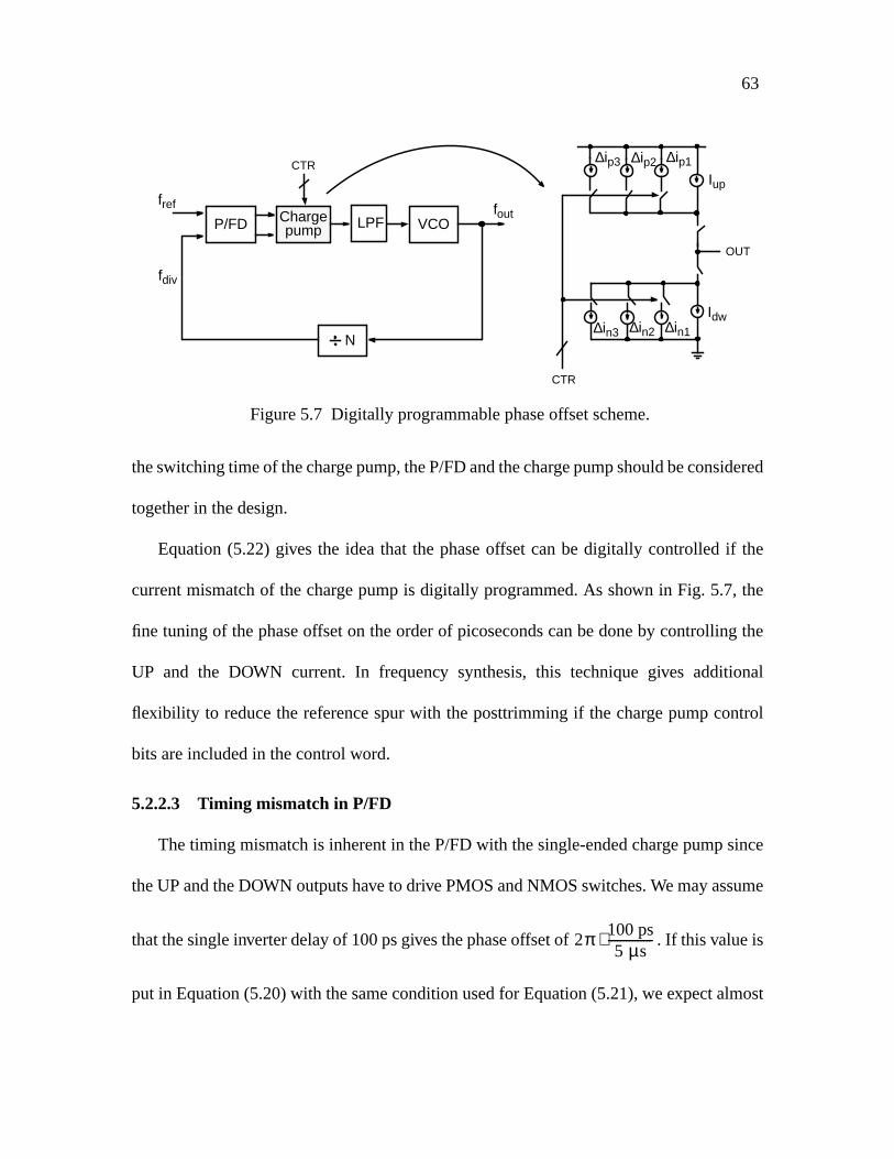
63
the switching time of the charge pump, the P/FD and the charge pump should be considered
together in the design.
Equation (5.22) gives the idea that the phase offset can be digitally controlled if the
current mismatch of the charge pump is digitally programmed. As shown in Fig. 5.7, the
fine tuning of the phase offset on the order of picoseconds can be done by controlling the
UP and the DOWN current. In frequency synthesis, this technique gives additional
flexibility to reduce the reference spur with the posttrimming if the charge pump control
bits are included in the control word.
5.2.2.3 Timing mismatch in P/FD
The timing mismatch is inherent in the P/FD with the single-ended charge pump since
the UP and the DOWN outputs have to drive PMOS and NMOS switches. We may assume
that the single inverter delay of 100 ps gives the phase offset of . If this value is
put in Equation (5.20) with the same condition used for Equation (5.21), we expect almost
CTR
Iup
Idw
∆ip1∆ip2∆ip3
∆in1∆in2∆in3
OUT
P/FD Charge VCO
N
fref
pump
fdiv
foutLPF
CTR
Figure 5.7 Digitally programmable phase offset scheme.
2π 100 ps5 µs
---------------⋅

64
-26 dBc spur, reaching to the wrong conclusion that the single gate delay mismatch in the
P/FD is far dominant over any mismatch in the charge pump. The effective FM noise due
to the timing mismatch in the P/FD, however, is also suppressed by the ratio of the turn-on
time of the P/FD to the reference period as illustrated in Fig. 5.8. When the delay mismatch
∆td is much smaller than the P/FD turn-on time∆ton, the amount of the spur is
approximately given by
(5.24)
By using Equation (5.24), the single inverter delay of 100 ps gives -64 dBc spur with the
same condition for Equation (5.21). Thus, the timing mismatch in the P/FD is less
significant compared to the leakage current or the mismatch in the charge pump.
fref
fdiv
UP
Effectiveoutput
DW
Figure 5.8 Phase offset due to P/FD mismatch.
Timing mismatch
Pspur 20f BW
f ref----------- N
2π( )2
2-------------
∆ton
T ref----------
∆td
T ref---------⋅⋅ ⋅ ⋅
20f ref
f P1---------
.
log–log≅

65
A closed-loop behavior simulation is done to verify the analysis. In Fig. 5.9, the spur
levels at 200-kHz offset in the VCO output are plotted with the nonideal conditions caused
by the leakage current, the charge pump mismatch and the P/FD mismatch. To reduce the
simulation time, a third-order PLL with the division value of only 4 is taken with the
reference frequency of 200 kHz. Since the division value is too small to measure the spur
level with the practical condition, the effect of the nonideal conditions are exaggerated to
get the sufficient spur level which is much higher than the numerical noise from the
simulator using the coarse time step. The loop bandwidth is about 16 kHz. The prediction
-60
-55
-50
-45
-40
-35
(10µA,1mA) (20µA,1mA)(5µA,1mA)
(25ns,0.8µs) (50ns,0.8µs)(25ns,0.4µs)
(1mA,1.1mA,0.5µs) (1mA,1.2mA,0.5µs) (1mA,1.2mA,1µs)
(a) (Ileak,Icp) ;
(b) (Iup,Idw,∆ton) ;
Ref
eren
ce s
pur
@20
0kH
z (d
Bc)
(c) (∆td,∆ton) ;
Figure 5.9 Closed-loop simulation of third-order PLL with nonideal effects(fref = 200 kHz,fBW = 16 kHz,fp1 = 80 kHz, andN = 4).
(a) with leakage current
(b) with current mismatch
(c) with P/FD mismatch
66
of the spur with the fourth-order PLL is straightforward when the spur level in the third-
order PLL is given. The results of each case are close to those obtained from the previous
analysis.
5.2.2.4 Spur by ∆−Σ modulator
In fractional-N frequency synthesizers, the∆−Σ modulator is an another source for the
spur generation. The idle tone of the modulator can cause the spur since the input of the
modulator is always dc. The dithering is useful to suppress the idle tone but cannot
eliminate the idle tone completely. The effect of the idle tone toward the spur in the
frequency synthesizer may be significant when the effect of the phase detector nonlinearity
is combined, as previously discussed. Another mechanism is the beat tone generated by the
harmonic of the phase detector frequency and the VCO output frequency. When the VCO
output frequency is close to the harmonic of the phase detector frequency, the tone is
generated at the corresponding offset frequency. Therefore, additional efforts are necessary
in fractional-N synthesizers to reduce the phase detector nonlinearity with the proper phase
detector design, and to minimize the harmonic coupling with careful layout floor-plan and
packaging.
5.3 Settling Time
Settling time indicates how agile the frequency synthesizer is to select the channel and
is an important factor in multi-slot wireless applications such as a GPRS system.

67
5.3.1 State variable description of PLL
A state variable description of the PLL helps to understand the internal system variables
such as the voltage across the capacitor in the loop filter, which cannot be described with
the input/output (I/O) transfer function [59], [60]. Figure 5.10 shows the equivalent model
of the type-2, second-order charge pump PLL with associated state variables. The phase
errorφ(t) and the voltagevc(t) across the capacitor in the loop filter are state variables of
the system. Then, the state variable equations are given by
(5.25)
whereICP is the charge pump output current. When the system is in a steady state, the state
variables must be constant. Then, the state equation in the steady state is given by
Figure 5.10 State-variable description of type-2, second-order charge-pump PLL.
Σ
VC(t)
ICP
KVCO
R
C ∫
Σ
∫
φ(t)θ(t)
1
dφ t( )dt
------------- KVCOV C t( )– KVCOICPR φ t( )⋅– dθ t( )dt
-------------+=
dV C t( )dt
-----------------ICP
C-------- φ t( ) ,⋅=
î

68
(5.26)
where the subscripts denotes the steady state of the state variables. If the input phase is
assumed to be a ramp, or
(5.27)
Then,
(5.28)
From Equation (5.28), the physical meaning ofVC(t) can be considered the control voltage
to retune the VCO by an amount of∆ω.
5.3.2 Slew rate of PLL
When the PLL is in frequency acquisition mode, the settling time is often limited by the
nonlinear behavior due to the large-signal operation. The nonlinear settling time analysis is
pretty similar to that of an op amplifier. While the op amplifier design considers the settling
time in the voltage domain, the PLL does in the frequency domain as shown in Fig. 5.11.
Similar to the op amplifier design, the slew rate of the PLL, SRPLL (Hz/s), based on
Equation (5.28) can be defined by
(5.29)
dφs
dt-------- 0 KVCOV Cs– KVCOICPR φs⋅–
tddθ+==
dV Cs
dt------------ 0
ICP
C-------- φs ,⋅==
î
θ t( ) ∆ωt, t 0≥0, t 0 .<î
=
V Cs∆ω
KVCO--------------
.=
SRPLL
ICP
C-------- KVCO ,
⋅=

69
where ICP is the charge pump output current, andC is the value of the capacitor that
determines the zero of the loop filter.
It is interesting to know whether the settling time is limited by slew rate. With the first-
order approximation, the frequency settling over time is given by
(5.30)
wherefo is the desired output frequency, andτn is the loop time constant or the inverse of
the natural frequency ωn. When the loop transient is not slew-limited, the slew rate of the
PLL with the frequency dividerN is higher than the slope of the function by Equation (5.30)
at t = 0, or
(5.31)
Figure 5.11 Settling time of PLL.
t
fε
f(t)
t1
ft1
SlopeIcp
CKvco=
Linear region
Nonlinear region
fo
f t( ) f o 1 e
tτn----–
–
,=
ICP
C-------- KVCO td
d f
t 0=
>⋅f o
τn----- f o
ICP
C--------
KVCO
N--------------⋅
.⋅= =

70
Then,
(5.32)
Therefore, the slew rate should be considered in the settling time when Equation (5.32) is
not satisfied. Note that the inverse relation of Equation (5.32) also implies the condition of
the maximum slope for the proper frequency ramping when the frequency acquisition aid
is done by ramping the VCO input voltage [16].
5.3.3 Settling time including slew rate
The settling time including the slew rate can be analyzed as illustrated in Fig. 5.11. The
frequency over time is described as
(5.33)
whereft1 is the boundary between the linear region and the nonlinear region, and it is given
by
(5.34)
In the lock-in range, the time for the PLL to be settled tofo within the frequency errorfε is
given by
(5.35)
ICP
C--------
f o2
N KVCO⋅-----------------------
.>
f t( )
ICPKVCO
C----------------------- t , t⋅ t1≤
f o f t1–( ) 1 e
tτn----–
–
, t t1 ,>
î
=
f t1ICPKVCO
C-----------------------t1 .
=
f o f t1–( )e
tτn----–
f ε .<

71
That is,
(5.36)
Then, the total settling time tsettle of the PLL is given by
(5.37)
wheret1 is obtained from Equation (5.33).
5.4 Frequency Accuracy and Resolution
In PLL-based frequency synthesizers, the output frequency accuracy is as good as that
of the reference source since the phase-lock technique guarantees the zero frequency error
in the locked condition. The required frequency accuracy is typically less than few ppm.
However, the frequency drift of the low-cost crystal oscillator is a concern, and it easily
degrades the system performance. As the∆−Σ modulated fractional-N synthesizer
generates the output frequency with an arbitrarily fine frequency resolution, the frequency
drift by the crystal oscillator can be compensated by the synthesizer. The frequency
resolution∆f of the synthesizer is determined by
(5.38)
whereN is the number of bits of the∆−Σ modulator andfPD is the phase detector frequency.
Such a fine frequency resolution also makes the synthesizer accommodate various crystal
oscillators without reducing the phase detector frequency, which is useful for the noise
performance.
tf o f t1–
f ε-------------------
τn .⋅ln>
tsettle t1
f o f t1–
f ε-------------------
τn ,⋅ln+=
∆ ff PD
2N
---------,
=

72
5.5 PLL Loop Parameter
For an oversampling ADC, the decimation filter is necessary to enhance the overall
dynamic range. In frequency synthesis, this filter cannot be used since the∆−Σ modulator
has to operate at the phase detector frequency for the best performance, as explained
previously. A PLL, however, will do a similar job since its transfer function suppresses the
high-frequency noise as a low-pass filter. Figure 5.12 shows the noise contribution of a
Figure 5.12 Overall synthesizer noise illustration with third-ordermodulator (not to be scaled).
fz fp1 fp2 freffunity
L(f)
f
+40dB/dec
Overall
PLL
VCO
Reference
Modulator
+20dB/dec -20dB/dec
0dB/dec

73
third-order modulator in a type-2, fourth-order PLL. As the quantization noise of the third-
order modulator has the slope of +40 dB/dec, the fourth pole is required to taper out the
quantization noise at high frequency. For example, a 40-kHz loop bandwidth will induce
theoretically less than -120 dBc/Hz in-band phase noise and the out-of-band noise is further
suppressed by the additional poles as seen in Fig. 5.12. Note that the quantization noise is
not multiplied by the division ratio when it is referred to the output phase noise of the
synthesizer, because it is generated by the frequency modulation having the resolution of
one VCO clock period.

74
CHAPTER 6
IMPLEMENTATION OF A 1.1-GHZ CMOS FREQUENCY SYNTHESIZER
Despite their high performance, fractional-N frequency synthesizers with on-chip∆−Σ
modulators have not been widely used in wireless handset applications due to their
hardware complexity and high power consumption. Low-cost and low-power CMOS
fractional-N synthesizers using the digiphase technique have not exhibited significantly
better noise performance compared to that of integer-N synthesizers. In this work, a 1.1-
GHz CMOS fractional-N synthesizer is implemented to meet most wireless applications,
including multi-slot GSM, AMPS, IS-54, CDMA (IS-95), and PDC. Among these
applications, the multi-slot GSM requires both agile switching and low noise performance,
and it is chosen as a target system in this work. The key specifications for the synthesizer
are listed below.
• Technology: 0.5-µm CMOS
• Output frequency: 880-960 MHz
• Frequency step: 200 kHz
• Frequency resolution: < 1 Hz
• Integrated noise: < 2o-rms with less than -125 dBc/Hz @ 600-kHz offset
• Spurious tones: < -55 dBc @ 200-kHz offset, < -75 dBc @ 400-kHz offset
• Settling time: < 250µs

75
6.1 System Architecture
Figure 6.1 shows the functional block diagram of the fractional-N frequency synthe-
sizer. All the synthesizer blocks are to be fully integrated except the VCO and the loop fil-
ter. Since a third-order∆−Σ modulator is used, a type-2, fourth-order PLL having two
additional out-of-band poles is designed to filter out the quantization noise of the modula-
tor at high frequencies. A standard frequency divider configuration is used with an 8/9
prescaler, a 3-b auxiliary counter, and an 8-b main counter, which results in a 11-b maxi-
mum division ratio. The use of 4/5 prescaler suffers from high power consumption by dig-
ital counters and the 16/17 prescaler suffers from the large minimum division ratio. The
asynchronous counters are used to save the power consumption, which will be explained
P/FD ChargeRFREFpump CPO
M P/P+1
A
Lockdetector
Controllogic
∆−Σmodulator
m
k
r sc
ds dat
sp
LD
RFINRFINB
Serial-to-parallel/selection logic
LECLKDAT
a
ctr
pd
Bias/reference
Figure 6.1 Functional block diagram of the synthesizer.

76
later. The system is configured to be compatible with existing integer-N frequency synthe-
sizers.
In this work, a tri-state charge pump with the P/FD is employed to avoid using an
active filter. It provides low power consumption with the passive loop filter and less sensi-
tivity to the substrate noise coupling even though the linearity performance may not be as
good as that of the active loop filter. The P/FD and the charge pump are designed to have
four different sets of the phase detector gain and to work with both positive- and negative-
gain VCO.
The band-gap reference circuit generates a temperature-independent output current for
the charge-pump. It also keeps the PLL bandwidth constant over temperature. The control
logic takes the 3-b output of the∆−Σ modulator and provides the randomized data to the
counters. A pseudorandom sequence with a length of 224 is used with LSB dithering. The
fine frequency resolution of less than 0.001 ppm can make the synthesizer compensate for
the crystal-frequency drift with a digital word. It can also accommodate various crystal
frequencies without reducing the phase detector frequency.
In the following sections, detailed design issues are discussed for major building
blocks, including the P/FD, the charge pump, the frequency divider, the bias cell, and the
digital cells.
6.2 P/FD
Providing frequency acquisition aid, the P/FD is a popular digital phase detector
combined with the charge pump in frequency synthesizer applications, while other

77
applications such as data-recovery systems employ different schemes [61]. The P/FD is
mostly implemented using either D-type master-slave flip-flops or R-S latches. The latter
offers higher speed than the former [62], but the improved edge-triggered D-type flip-flop
shown in Fig. 6.2 makes it possible to have the P/FD achieve high timing resolution [63].
It also has the small number of transistors, which helps to reduce the noise contribution by
P/FD.
The dead-zone of the P/FD is a concern since it degrades the noise performance by
reducing the open-loop gain of the PLL in the locked condition. This cross-over distortion
is mainly caused by the insufficient turn-on time for the charge pump when the P/FD
generates the pulse width for a small phase error. It can be avoided by giving an additional
delay for the reset time in the P/FD to provide an enough turn-on time. Two factors
determine the minimum turn-on time of the P/FD. One is the capacitance loading at the
output of the P/FD. The time constant given by the channel resistance of the output
Figure 6.2 Modified D-type P/FD.
CLK1 UP
DW
D Q
INHB
DLY
D QINHB
CLK2
D
Q
INHB

78
transistor and the load capacitance determines the falling (or rising) time above the
threshold voltage to turn on the UP (or DW) switch. This effect can be minimized by having
proper transistor size at the output stage. The other comes from the charge-pump turn-on
time itself. Since the charge pump output current is completely turned off in the tri-state
mode, the turn-on time of the current mirror determines the minimum turn-on time of the
P/FD, which is usually a dominant factor in the design of high-performance charge pumps.
6.3 Charge Pump
The tri-state charge pump is popular in frequency synthesizer applications since it
makes a type-2 PLL possible with the passive loop filter. It also provides low power con-
sumption with tri-state operation. In the standard integer-N frequency synthesizer, the out-
put current of the charge pump can be as high as 10 mA [64] to provide better spur
performance over the leakage current and to have high SNR at the output of the charge
pump for low noise contribution to the PLL. With tri-state operation, the current consump-
tion of the charge pump in the locked condition is lower than few hundredµA depending
on the phase detector frequency and the turn-on time of the P/FD. The use of a tri-state
charge pump is also important to minimize the substrate noise coupling when the∆−Σ
modulator is on the same die. By turning it on briefly between the rising and the falling
edges of the reference, the substrate noise coupling can be significantly reduced.
Three typical topologies are shown in Fig. 6.3. First one in Fig. 6.3(a) is the charge
pump with the switch at the drain of the current mirror MOS. When the switch is turned
off, the current pulls the drain of M1 to ground. After the switch is turned on, the voltage

79
at the drain of M1 increases from 0 V to the loop filter voltage held by PLL. In the mean-
time, M1 has to be in the linear region till the voltage at the drain of M1 is higher than the
minimum saturation voltage∆1. During this time, high peak current is generated even
though the charge coupling is not considered. The peak current is generated from the two
series turn-on resistors of the current mirror and the switch having the voltage difference
equivalent to the output voltage. On the PMOS side, the same situation will occur and the
matching of this peak current is difficult since the amount of the peak current varies with
the output voltage. Figure 6.3(b) shows the charge pump where the gate is switched
instead of the drain [65], [66]. With this topology, the current mirrors are guaranteed to be
in the saturation region. To achieve fast switching time, however, the bias current of M3
and M4 may not be scaled down since the transconductancegm affects the switching time
constant in this configuration. The gate capacitance of M1 and M2 is substantial when the
output current of the charge pump is high and when the long channel device is used for
OUTIUP
UP
DW
M2
M1 M3
M4
IDW
OUT
DW
UP
M2
M1M3
M4
IUP
IDW
OUT
UP
DW
M2
M1 M3
M4
IUP
IDW
(a) (b) (c)
Figure 6.3 Single-ended charge pumps: (a) switch in drain, (b) switch in gate,and (c) switch in source.

80
better matching. To save the constant bias current, the gated bias current can be employed
cooperating with the PLL at the cost of complexity [67]. The switch can be located at the
source of the current mirror MOS as shown in Fig. 6.3(c) [68]. M1 and M2 are in the satu-
ration all the time. Different from the gate switching, thegm of M3 and M4 does not affect
the switching time. As a result, the low bias current can be used with high output current.
This architecture gives faster switching time than the gate switching due to low parasitic
capacitance seen by the switches.
In addition to the typical configuration discussed previously, some variations are done
to improve the performance. Figure 6.4(a) shows the charge pump with an active amplifier
[69], [70]. With the unity gain amplifier, the voltage at the drain of M1 and M2 is set to
the voltage at the output node when the switch is off to avoid linear-region operation of
M1 and M2 and to reduce the charge sharing effect when the switch is turned on. Another
one is the charge pump with the current steering switch as shown in Fig. 6.4(b). The per-
OUTUP
DW
IDW
IUP
UPB
DWB
OUT
IUP
UPM2
M1M3
M4
IDW
DWDWB
UPB
(a) (b)
Figure 6.4 Variations of single-ended charge pumps: (a) with active amplifier,(b) with current-steering switch, and (c) with NMOS switches only.
OUT
M5
M1M2
M6
DWDWB
M3 M4UP UPB
ICP ICP
(c)

81
formance is similar to the one shown in Fig. 6.3(a), but the switching time is improved by
using the current switch. This structure provides high-speed single-ended charge pump. In
Fig. 6.4(c), the inherent mismatch of PMOS and NMOS is avoided by using only NMOS
switches [71]. However, the current mirrors, M5 and M6, limit the performance unless
large current is used. Since the current does not flow in the current mirror when UP switch
is turned off, this architecture is still far from the differential topology. From the above
investigation, the source switching is considered attractive due to the simple structure, low
power consumption and comparable switching time.
Figure 6.5 shows the schematic of a programmable charge pump designed to minimize
the turn-on time of the P/FD without creating a dead zone. Having the switches, M1, M2,
M19, and M20, at the source of the current mirror improves the switching speed while
M3
M21
M12
M8
M14
M17
M15
M18
BIAS2 M10
M6
M2
M20
M11
M7
M4
VDD
VDDMC1
MC2
BIAS1
ICP
M13
M16
DW
M9
M5
M1
M19UP
OUT
bi
bi
bi
bi
MS1
MS3
MS4
MS2
PDB
PD
MD2
MD1
Figure 6.5 Programmable charge pump.

82
keeping the switching noise low. Current mirrors, M5 - M18, are cascoded to increase out-
put impedance, and four different output currents can be generated with the control bitbi
at each stage. The capacitors MC1 and MC2 are added to reduce the charge coupling to
the gate and to enhance the switching speed. The control bit PD and the complementary
bit PDB force the current mirrors to be turned off during the power-down mode. Note that
the P/FD and the charge pump are triggered at the falling edge of the clock to reduce the
substrate noise coupling because the∆−Σ modulator is triggered at the rising edge. The
clock for the∆−Σ modulator is slightly delayed so that the turn-on time of the P/FD can be
separated from the falling edge of the clock for further reduction of the substrate noise
coupling. The output voltage compliance of the charge pump is designed to be larger than
the range of 0.5 to 2.5 V with 3-V supply over process and temperature variations.
In fractional-N frequency synthesis, the phase detector linearity is important to lower
the in-band noise and the idle tones. The simulation result in Fig. 6.6 shows the relation
between the phase detector linearity and the minimum turn-on time of the charge pump.
Accumulated charges after 7 clock cycles are plotted for each phase offset using different
charge pumps that require different minimum turn-on time combined with the P/FD. Note
that the minimum turn-on time shown in Fig. 6.6 and the actual turn-on time used in the
P/FD may be independent. For example, the charge pump having the minimum turn-on
time of 3.4 ns with the P/FD turn-on time of 28 ns produces better linearity than the charge
pump with the P/FD minimum turn-on time of 28 ns. Less minimum turn-on time in the
plot implies better phase resolution of the phase detector, and it can be done by faster charge
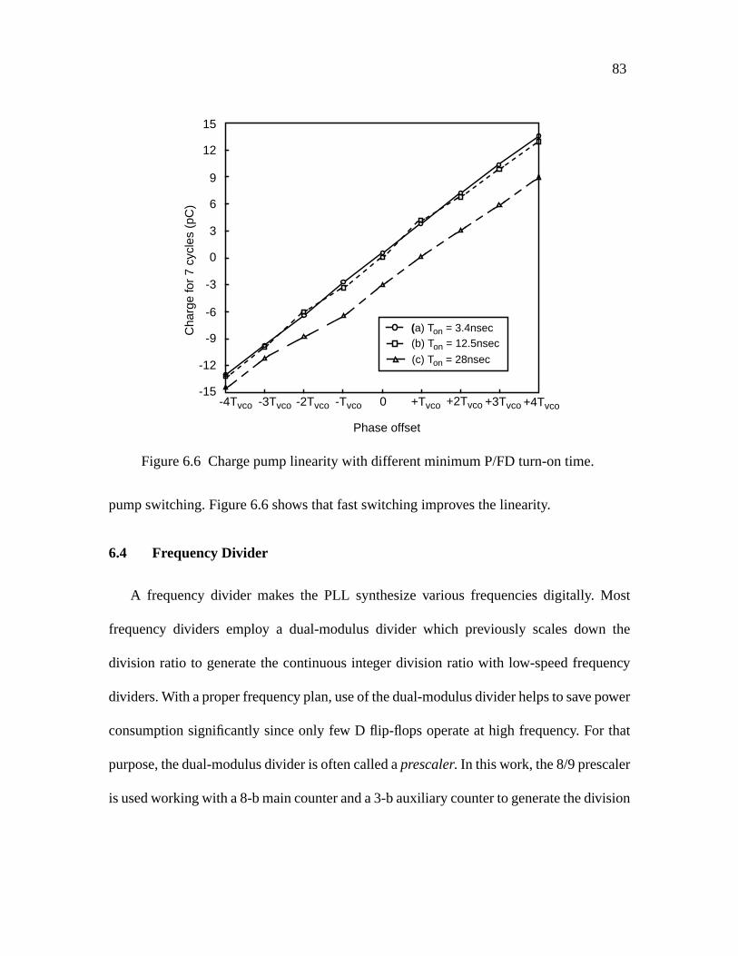
83
pump switching. Figure 6.6 shows that fast switching improves the linearity.
6.4 Frequency Divider
A frequency divider makes the PLL synthesize various frequencies digitally. Most
frequency dividers employ a dual-modulus divider which previously scales down the
division ratio to generate the continuous integer division ratio with low-speed frequency
dividers. With a proper frequency plan, use of the dual-modulus divider helps to save power
consumption significantly since only few D flip-flops operate at high frequency. For that
purpose, the dual-modulus divider is often called aprescaler. In this work, the 8/9 prescaler
is used working with a 8-b main counter and a 3-b auxiliary counter to generate the division
0
3
6
9
12
15
(a) Ton = 3.4nsec(b) Ton = 12.5nsec
(c) Ton = 28nsec
Cha
rge
for
7 cy
cles
(pC
)
-3Tvco-4Tvco -Tvco-2Tvco +3Tvco +4Tvco+Tvco +2Tvco0-15
-12
-9
-6
-3
Phase offset
Figure 6.6 Charge pump linearity with different minimum P/FD turn-on time.

84
ratio from 82 – 8 (= 56) to 211 – 1 (= 2047).
6.4.1 Prescaler
The 8/9 prescaler is designed in fully differential current-mode logic (CML) to have
low supply and substrate noise. To save power consumption, it is designed with a 4/5
divider and a toggle flip-flop, where the 4/5 divider works as a prescaler within the 8/9
divider. Figure 6.7 shows the master-slave D flip-flop in CML with an embedded OR gate
which is used in the 4/5 divider [9], [72]. The resistor is used as a passive load to reduce
parasitic capacitance and to improve the noise performance. The drain of the transistor M8
and the source of the transistor M7 are merged in the layout to improve the operating speed.
Note that the source follower is not necessary at the end of each block in CMOS design,
which helps to reduce power. The minimum channel length is chosen for each transistor
Figure 6.7 DFF with embedded OR gate in 4/5 prescaler.
A
C1
A
B
B
CK
CK
BIAS
R1 R2 R3 R4
M1 M2
M3 M4 M5 M6
M8
M7M9
M10M11 M12 M13M14 M15 M16

85
except for the current mirrors. TheW/L ratio of each transistor depends on the bias current.
It should be carefully determined by considering the tradeoff between the input sensitivity
and the speed. The minimumW/L ratio significantly improves the speed by having low
parasitic capacitance, but it might have the differential switch not turned on completely due
to the increased minimum saturation voltageVDS,SAT. Since the signal amplitude varies a
lot over temperature, theW/L ratio should be chosen with enough margin over temperature
and process variations.
Different from other RF circuits, prescalers operate in the large-signal mode except the
preamplifier. It means that the phase noise is primarily determined at the zero-crossing
time, where the bias current noise is considered a common-mode noise. Therefore, the
matching between the resistor loads is important since the mismatch gives the input-
referred dc offset, and it will convert the common-mode noise either by the bias current or
by the supply to the equivalent differential input noise. Large signal swing also improves
the noise performance with the increased power consumption. In this work, the signal
swing of 0.8 Vpeak is used. For further improvement, the use of cascoded current mirrors
will help to reduce the noise contribution from bias current by having high common-mode
rejection and by reducing the charge coupling to the gate of the current mirror through the
parasitic capacitance between the drain and the gate.
The preamplifier or the RF input buffer is designed to provide enough signal level to
drive the 4/5 prescaler from the external VCO. To accommodate various systems, the RF
input sensitivity needs to be as low as -15 dBm. Three differential amplifiers and source
followers in the last stage are used, and the differential input stage is designed with proper

86
dc biasing requiring the external ac coupling capacitor. Since the external VCO does not
provide differential output, only one pin is connected to the VCO and the other pin is ac-
grounded.
CNT–MIN
Trigger
P/P+1 DFF OUT(1) (2)
(Async.)
CNT–A DFF(Async.)
(3)
(4)
(5) (6)
(1)
td<7nsec
td1 ttrig
(2)
(3)
(4)
(5)
(6)
td2 AM
Figure 6.8 Locally asynchronous, globally synchronous modulus controller andtiming diagram example (M = 8, A = 3).

87
6.4.2 Digital counters
Since the digital counters operate at higher than 120 MHz for the 1.1-GHz output with
the 8/9 prescaler, the asynchronous counters are used to save the power consumption. The
block diagram is shown in Fig. 6.8 with the timing diagram example when the data of the
main counter and of the auxiliary counter are 8 and 3, respectively. The waveform (3) is
the main divider output or the input of the P/FD, and the waveform (6) is the modulus con-
trol where 3 clock cycles are used forP + 1 division and 8 – 3 (=5) clock cycles are used
for P division. The logic delay due to the asynchronous operation in addition to the delay
of the CML-to-CMOS converter gives stringent timing requirement for the modulus con-
trol resulting in more power consumption in the CML-to-CMOS converter. To absorb the
logic delays in the asynchronous operation, a D flip-flop is added at the output of the
counter triggered by the input clock. It also prevents the jitter from accumulating in the
asynchronous counter.
6.5 Logic Converters
Since the prescaler is designed in CML, the CML-to-CMOS converter is needed for the
prescaler to drive digital counters as the CMOS-to-CML converter is required by the
modulus controller. Figure 6.9(a) shows the schematic of the CML-to-CMOS converter.
This block is a pretty sensitive portion of the synthesizer to the supply and substrate noise
coupling since the differential signal is converted to the weak single-ended signal and then
amplified. More power consumption is used to achieve better immunity to the noise
coupling than required for slew rate. Since the NMOS pulling is faster than the PMOS

88
Figure 6.9 Logic converters: (a) CMOS-to-CML, and (b) CML-to-CMOS.
M1INP
BIAS
OUTINN
(a)
(b)
M2
M3 M4
M5 M6M7 M8
M9 M10
M11 M12 M13
M14
M15
IN
OUT
OUTB
BIAS
R1 R2
M5
M3
M1
M2
M4

89
pushing at the output stage, theW/L ratio of the inverter M14 and M15 is designed to have
lower logic threshold than VDD/2. Note that the supply for the analog portion and for the
digital inverters needs to be separate for better isolation.
Since the CML-to-CMOS converter conveys the modulus control of the prescaler, the
noise consideration is not necessary in the design. As shown in Fig. 6.9(b), a simple
differential stage is used with the resistor load that sets the CML level.
6.6 Bias Circuit
A fully on-chip bias generation circuit is designed [73]. To enhance the supply
regulation and matching, the current mirrors are cascoded and more than 10-µm channel
length is used for all the transistors. The temperature-independent bias current is generated
for the charge pump to maintain the constant PLL bandwidth over temperature. The
modified bandgap reference circuit is used to compensate the temperature variation of the
n-poly resistor. It also prevents the prescaler from being too slow due to the increased
voltage swing at high temperature. Since the on-chip resistor is used to generate the current,
each block is designed to overcome more than 20% process variation in addition to
temperature variation.
6.7 Multi-Bit Modulator and Control Logic
The ∆−Σ modulator implementation based on the architecture shown in Fig. 6.10 is
straightforward since it is a pure digital block. The digital modulator is implemented based
on the two’s complement binary system for subtraction, and the output data of the

90
modulator –4, –3, ..., +2, +3 are converted to the input data for the multi-modulus divider
0, +1, +2, ..., +6, +7, resulting in the division ratio offset of 3.5 when the input data of
the modulator are all zeros. In order to eliminate any audible tone due to the repetition of
the sequence, the fractional modulo of 224 is used with LSB dithering to have the sequence
length span several seconds. For example, when the clock frequency is 8 MHz, the
repetition time of the pseudorandom sequence is 224/8 MHz = 2.1 s.
Since the multi-bit modulator or the MASH modulator generates the multi-bit output,
a multi-modulus divider is necessary. However, a standard divider configuration having the
dual-modulus divider can be used if the modulated data are provided to each counter with
the control logic. As shown in Fig. 6.10, the 3-b modulator output is added to the 11-b input
data for the counters to generate the modulated input data. The overflow is neglected since
the typical division ratio is far less than 211 for fractional-N synthesizers. Each data is
Figure 6.10 Multi-bit modulator and control logic.
∆−Σ24
8/9
DFF
P/FD
modulator
Maincounter
Σ3 12
Aux.counter
Trigger
8
3
VCO
CLK
DAT
11
K

91
synchronized with the output clock of the main counter. Note that the data for each counter
should be updated at the rate of the output frequency of the 8/9 prescaler.
6.8 Data Interface and Selection Logic
Because of large number of control inputs in frequency synthesizer, the control bits are
provided to each block through the serial-to-parallel interface using a 3-wire bus which
consists of the clock signal (CLK), the data signal (DAT), and the load enable signal (LE).
As shown in Fig. 6.11(a), the serial-to-parallel interface transforms the serial data to the 26-
b parallel data. The 2-b address word selects the corresponding latch block while disabling
other latch block, and the 24-b control word is loaded to each latch block. Figure 6.11(b)
shows the word map used in this work to program the synthesizer.
6.9 Loop Filter
Since the PLL acts as a decimation filter for the oversampling output data, a fourth-
order PLL is required to filter out the out-of-band quantization noise of the third-order
modulator which has the phase noise density slope of +40 dB/dec. Figure 6.12 shows the
third-order loop filter using only the resistors and the capacitors.
The loop filter is designed as follows [23]. The external VCO having the sensitivity
KVCO of 25 MHz/V is used and the charge-pump output currentICP is set to 640µA. For
the 900-MHz output with the 8-MHz phase detector frequency, the division ratioN is about
112. The loop filter is designed to have shorter settling time than the specification to
accommodate the process variations of the VCO gain and the charge pump output current.

92
Fig
ure
6.11
(a)
Dat
a in
terfac
e an
d se
lect
ion
logi
c, a
nd (
b) c
ontr
ol w
ord
map
.
Latc
h(P
LL)
S-t
o-P
24
LEDAT
(a)
(b)
2
inte
rfac
e
CLK
Latc
h
24 24
(Mod
ulat
or)
Con
trol
wor
d1
Con
trol
wor
d2LE
cont
rol
D 0
D 1
D 2
D 21
D 3
D 4
D 5
D 6
D 7
D 8
D 9
D 10
D 11
D 12
D 13
D 14
D 15
D 16
D 17
D 18
D 19
D 20
D 25
D 22
D 23
D 24
1 1
0 1
Ref
eren
ce d
ivid
erM
ain
divi
der
∆−Σ
mod
ulat
or
PD
gai
n &
Pow
erco
ntro
lpo
larit
y

93
The natural frequency fn of the synthesizer having the frequency errorfe of 100 Hz to have
less than 150-µs settling timets for the frequency jump fstep of 100 MHz is given by
(6.1)
where the damping factorζ of 0.7 is assumed. The capacitorC1 that creates the zero of the
loop filter is determined by
(6.2)
Then, the resistorR1 is given by
(6.3)
The capacitorC2 of 560 pF is used to have the 3rd-pole of the PLL at about 160 kHz. The
values of the resistorR2 and the capacitorC3 are chosen to have the fourth-pole at 260 kHz.
f n1–
2πtsζ--------------
ζ f e×f step
---------------
27 kHz ,≅ln⋅=
Figure 6.12 3rd-order loop filter.
Charge pump
C1
C2R1
C3
R2VCO
(560pF)
(4.9nF)
(60pF)(1.68kΩ)
(10kΩ)
C1
ICP KVCO×
N 2π f n×( )2×------------------------------------- 4.9 nF .≅=
R1 2ζ NICP KVCO C1⋅ ⋅----------------------------------------× 1.68 kΩ .≅=

94
The slew rate defined by Equation (5.29) is about 3.3 MHz/µs and can be neglected. In this
work, the loop is designed to be overdamped by increasing the value of the capacitorC1
even though the phase margin of about 50o is known to be optimal for the settling time. The
overdamped loop suppresses the phase noise peaking around the loop bandwidth and helps
to analyze the phase noise contribution of each source including the∆−Σ modulator.

95
CHAPTER 7
EXPERIMENTAL RESULTS
The prototype synthesizer with second and third-order∆−Σ modulators was fabricated
in 0.5-µm CMOS and packaged in a 32-pin thin quadrature flat package (TQFP). The die
photo is shown in Fig. 7.1. The chip area is mm2, including two other MASH
modulators. Each modulator is selected with an external 2-bit control word. As mentioned
previously, the synthesizer is fully programmable through a 3-wire bus from a PC.
Figure 7.2 shows the measured output spectrum at 900.03 MHz with the 3-b second-
and third-order∆−Σ modulators. They are compared by switching the output bits of each
modulator without changing any loop parameter of the synthesizer. The external loop filter
is designed to have about 40-kHz loop bandwidth for the 900-MHz output with the 8-MHz
phase detector frequency, or with the division ratio of about 112. The third-order modulator
case shows less out-of-band noise as expected. With the 8-MHz phase detector frequency,
-45-dBc spur appears at about 60-kHz offset and it is suppressed to -80 dBc with the 3-kHz
loop bandwidth. However, no fractional spur was observed when the phase detector
frequency is set to 7.994 MHz. From the experiment, the spur results from the relation
between the output frequency and the phase detector frequency, and it becomes more
significant when the output frequency approaches the rational multiples of the phase
detector frequency. For example, when the output frequency is set to 900.03 MHz with the
8-MHz phase detector frequency, the division ratio is 112.5 + 0.0375. The idle tone near
the half clock frequency is given by (3.14).
3.16 3.49×
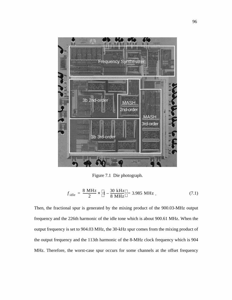
96
(7.1)
Then, the fractional spur is generated by the mixing product of the 900.03-MHz output
frequency and the 226th harmonic of the idle tone which is about 900.61 MHz. When the
output frequency is set to 904.03 MHz, the 30-kHz spur comes from the mixing product of
the output frequency and the 113th harmonic of the 8-MHz clock frequency which is 904
MHz. Therefore, the worst-case spur occurs for some channels at the offset frequency
Figure 7.1 Die photograph.
Frequency Synthesizer
3b 3rd-order
3b 2nd-order
MASH
3rd-order
MASH
2nd-order
f idle8 MHz
2------------------ 1 30 kHz
8 MHz------------------–
3.985MHz .=×=

97
which is equivalent to the channel spacing of the system, and it is independent of the
frequency resolution of the synthesizer.
Being limited by the synthesizer noise, the output phase noise does not show the noise
shaping effect by the∆−Σ modulator unless the loop bandwidth is further increased.
However, the effect of the quantization noise from the∆−Σ modulator can be seen at the
divider output. Figure 7.3 shows the shaped quantization noise seen at the divider output.
The output with the second-order modulator has idle tones at high frequencies but they can
be suppressed to a negligible level at the VCO output with a 40-kHz loop bandwidth. The
third-order modulator does not exhibit high-frequency tones nearfs/2. Note that the corner
frequency of the quantization noise is close to that of the NTF shown n Fig. 4.5(b).
Figure 7.2 Measured spectrum at the VCO output.
2nd-order
3rd-order
98
Figure 7.4 shows the reference spur performance and the 7.994-MHz reference spur
was not measurable with a 40-kHz loop bandwidth. The spur level is estimated to be less
than -95 dBc since -88 dBc reference spur is measured with the 4-MHz phase detector
frequency for the same output frequency. It is found that -85 dBc spur shown at around 5-
MHz offset comes from the equipments not from the synthesizer board, because it was also
observed in the integer-N mode with different phase detector frequencies.
Figure 7.5 shows the synthesizer output phase noise measured at 900.03 MHz. The
phase noise of a free-running external VCO is plotted together. As shown in Fig. 7.5, the
phase noise of -92 dBc/Hz at 10-kHz offset frequency is achieved. The phase noise floor
from 200 to 800 kHz is the residual quantization noise of the modulator. The phase noise
is -135 dBc/Hz at 3-MHz offset frequency, and it can be further suppressed either by
Figure 7.3 Measured spectrum at the divider output.
2nd-order
3rd-order
99
Figure 7.4 Measured reference spur.
Figure 7.5 Measured open-loop and closed-loop output phase noises.
Open-loop
Closed-loop

100
increasing the phase detector frequency or by pushing high-order poles toward the loop
bandwidth sacrificing the phase margin.
Figure 7.6 shows the frequency divider output in the locked condition measured by the
digital oscilloscope. There was difficulty in triggering the modulated divider output with
the reference clock, and a short-duration performance was measured. The modulated
divider output has less than 2.5-ns peak-to-peak jitter, which shows that it swallows at most
2 VCO cyclesTVCO. In other words, the frequency divider modulation is performed with
at most 3 integer division values.
Figure 7.7 shows the fractional spur performance over frequency channels having 200-
kHz step with the phase detector frequency of 8 MHz. Most channels do not exhibit
TVCO TVCO
Figure 7.6 Measured modulated divider output in time domain.

101
fractional spur up to -85 dBc. However, the 400-kHz spur is shown when the output
frequency is set to 899.8 MHz or 900.2 MHz, which are close to 112.5 times 8 MHz, and
the 200-kHz spur is shown with the 400-kHz spur as a second harmonic when the output
frequency is set to 903.8 MHz or 904.2 MHz, which are close to 113 times 8 MHz. Almost
same spur performance is observed at around 908 MHz and 912 MHz, showing that the
fractional spur performance does not depend on the integer-N division ratio.
Figure 7.8 shows the fractional spur performance with different offset frequencies from
the output frequency of 904 MHz. For example, the -55-dBc spur is measured for the output
frequency of 900.16 MHz with the 40-kHz loop bandwidth. The spurs within the loop
bandwidth have the similar magnitude regardless of the offset frequency. The out-of-band
spur is suppressed substantially by the loop filter as the offset frequency increases. Even
Figure 7.7 Measured fractional spur vs. output frequency (fPD = 8 MHz).
-90
-80
-70
-60
-50
-40
200-kHz spur
400-kHz spur
Output frequency (MHz)
Frac
tiona
l spu
r (d
Bc)
898 899 900 901 902 903 904 905
400kHz
400kHz
800kHz

102
though the spurs are observed, the overall performance exceeds that of any integer-N
synthesizers reported to date. For example, when the output frequency is programmed in a
200-kHz step with the phase detector frequency of 6.4 MHz and the loop bandwidth of 15
kHz, the worst-case spur at 200-kHz offset is below -85 dBc for all channels and the in-
band phase noise is as low as -90 dBc/Hz.
Another interesting result that is not present in integer-N synthesizers is the noise-
shaped reference spur, which shows that the noise shaping is related with the digital
modulation. The noise shaping at the carrier is not clear since it may also come from the
phase noise peaking due to low phase margin, but the noise shaping at the reference spur
cannot be achieved in integer-N synthesizers. Several features observed in∆−Σ modulated
Figure 7.8 Measured fractional spur vs. offset frequency (fo = 904 MHz + offset).
-80
-70
-60
-50
-40
Offset frequency (kHz)
Frac
tiona
l spu
r (d
Bc)
5 10 20 40 80 160 320
-30

103
fractional-N synthesizers that are not present in integer-N synthesizers are summarized as
follows.
• Arbitrarily fine frequency resolution
• Fractional spur for some channels
• Residual out-of-band noise floor with low OSR
• Noise shaped reference spur
Among them, the residual out-of-band noise floor can be suppressed to a negligible level
when the synthesizer is designed with high OSR.
The chip works at 1.1 GHz with an input sensitivity of -15 dBm. The third-order
modulator consumes 1.4 mA at 1.5 V. The total current consumption of the synthesizer is
10.8 mA where 5 mA is consumed by the RF input buffer and 1.9 mA by the prescaler. The
measured bandgap voltage is 1.119 V and shows less than 1-mV variation over 2.7 – 4.0 V
supply. The measured performance is summarized in Table 7.1 Having about 3-kHz loop
bandwidth, the prototype synthesizer is useful for AMPS, IS-54, CDMA (IS-95), and PDC
applications. It can be also employed for multi-slot GSM application with a 40-kHz loop
bandwidth. Table 7.2 shows the performance comparison with the previously published
works. Without increasing the phase detector frequency and the oversampling ratio, the
noise performance of this work is comparable to that of the synthesizer with the fourth-
order MASH modulator that used a 20-MHz reference on the separate CMOS die [1].

104
Table 7.1 Summary of the measured performance.
Supply voltage
Supply current
Max. output frequency
Min. frequency resolution
Phase noise @10-kHz offset
Spurious tones
RF input sensitivity
2.5 - 4 V
* fo = 900.03 MHz, fpd = 7.994 MHz, and loop BW = 40 kHz.
10.8 mA
1130 MHz
< 1 Hz
– 15 dBm
< – 92 dBc/Hz*
< – 95 dBc*
< 10µA (stand-by)
< – 80dBc**
** fo = 900.03 MHz, fpd = 8 MHz, and loop BW = 3 kHz.
(2.7V analog, 1.5V digital)
Table 7.2 Performance comparison with existing arts.
Ref. Tech. Arch. fo fPD noiseIn-band
spurfBW
fPD
fBWRef.
Filiolet al. [1]
Perrottet al. [2]
Milleret al. [30]
Rileyet al. [29]
Thiswork
CMOS(∆−Σ)BJT(PLL) MASH
4th-order
0.6µmCMOS
0.5µmCMOS
Discrete
Discrete
MASH2nd-order
MASH3rd-order
3-bit3rd-order
1-bit3rd-order
(from PC)
915 MHz
1.8 GHz
405 MHz
(ext. /2)
750 MHz(ext. /2)
900 MHz
20 MHz
20 MHz
10 MHz
8 MHz
200 kHz
100 kHz
84 kHz
30 kHz
750 Hz
40 kHz
-95 dBc/Hz
-74 dBc/Hz
-85 dBc/Hz
-70 dBc/Hz
-92 dBc/Hz
-90 dBc
-60 dBc
>-82 dBc
>-133 dBc
-95 dBc
200
238
333
267
200

105
CHAPTER 8
CONCLUSIONS
Use of integer-N frequency synthesizers is limited for next-generation RF transceivers
due to the fundamental trade-off between the channel spacing and the loop bandwidth.
Providing agile frequency selection and superior noise performance, fractional-N
frequency synthesis is considered an ultimate solution for wireless applications. The∆−Σ
modulation method provides arbitrarily fine frequency resolution and becomes the
dominant spur reduction technique as CMOS technology advances.
Previous works mostly focus either on the∆−Σ modulator or on the PLL, and the design
aspects considering both blocks have not been well discussed. The research shows that a
multi-bit modulation technique improves the synthesizer performance by reducing high-
frequency jitter at the phase detector output. The phase detector linearity problem is
identified and discussed. To enhance the phase detector linearity, the charge pump with high
timing resolution is designed. Also, the tri-state charge pump is employed to have better
immunity to the substrate noise coupling due to the digital switching. A 1.1-GHz CMOS
fractional-N frequency synthesizer with a 3-b third-order∆−Σ modulator is implemented to
achieve better in-band phase noise, lower spurs, and faster settling time than those of
standard integer-N synthesizers. Synthesizing 900 MHz with 1-Hz resolution, it exhibits an
in-band phase noise of -92 dBc/Hz at 10-kHz offset with a reference spur of less than -95
dBc. Experimental results show that the proposed system is applicable to low-cost, low-

106
power wireless applications meeting the requirements of most RF applications including
multi-slot GSM, AMPS, IS-54, CDMA (IS-95), and PDC.
For extensions of this work, the VCO and the loop filter may be integrated to realize the
fully monolithic frequency synthesizer that requires no external component. With an on-
chip VCO, the wideband fractional-N frequency synthesis is more useful to suppress the
phase noise of the VCO. The substrate noise coupling to the on-chip VCO by the digital
modulation is to be further investigated. The interpolative frequency division technique is
not limited only to the fractional-N frequency synthesizers. It is applicable to the DDFS as
a spur reduction scheme and to FM modulators and demodulators. Consequently, this
research also demonstrates the feasibility of a general modulation method by oversampling
to build robust communication systems.

107
#include <stdio.h>#include <malloc.h>#include <math.h>
#define pi 3.141592654#define Seed 3#define Sigma 1.1
/* Normalized PLL Loop Parameter *//* reference;0.01Hz */#define f_clk .01/* LPF; 500 Ohm */#define R 500./* LPF; 7F */#define C 7./* charge pump; 1mA */#define Ip 1.e-3/* VCO; 0.01Hz */#define fo_vco .01/* VCO gain; .002 Hz/V */#define K_vco .002
/* Time Frame Set Up */#define rate_resol 1000.0#define cycle_max 7000#define t_delay_clk 0. /* 0 nsec */#define t_delay_vco 0. /* 0 nsec */#define plot_start1 400000#define plot_start2 0
extern long random();double Ranuni();double Pow();double Rangaus();double Div;
main()int clk, vco, vco_1, div;int clk_value, div_value;int up, down;
int rise_clk, fall_clk;int rise_div, fall_div;int first_fall_vco;int rise_vco, fall_vco;int cycle_clk;int half_cycle_clk, half_cycle_div;int count_error, acc;double t, t_start, t_final, t_res;double count_clk, count_div;double f_vco, To_vco;double vco_sin;double T_clk, T_half_clk;double Ip_eff;double V_vco_eff, V_vco, V_c;double noise_vco, noise_vco_lp;double phase_clk, phase_div;double phase_error;
To_vco = 1./fo_vco;T_clk = 1./f_clk;t_res = To_vco/rate_resol;t_start = 0;t_final = (double)cycle_max *To_vco + t_delay_vco;clk_value = 0;div_value = 0;first_fall_vco = 1;up = 0;down = 0;V_c = 0;V_vco = 0;V_vco_eff=0;T_half_clk = 0;half_cycle_clk = 0;half_cycle_div = 0;phase_clk = 0;phase_div = 0;count_error = 0;acc = 0;noise_vco_lp = 0;FILE *fo1, *fo2, *fo3, *fo4, *fo5,
APPENDIX A
PROGRAM LISTING
A.1 Behavioral Model Simulation Program for Second-Order PLL

108
*fo6, *fo7, *fo8;fo1 = fopen(“pll_vco.dat”, “w”);fo2 = fopen(“pll_vco_sin.dat”,“w”);fo3 = fopen(“pll_clk.dat”, “w”);fo4 = fopen(“pll_clk2.dat”, “w”);fo5 = fopen(“pll_phase_err.dat”,“w”);fo6 = fopen(“pll_phase_err2.dat”,“w”);fo7 = fopen(“pll_qp.dat”, “w”);fo8 = fopen(“pll_noise.dat”, “w”);
srandom(Seed); /* gaussian randomnumber */Div = Pow(2.0,31);
for(t=t_start;t<=t_final;t=t+t_res)/* set up time frame *//* VCO */rise_vco = 0; fall_vco = 0;noise_vco = Rangaus(Sigma);
/* Gaussian Random Number *//* noise_vco_lp = noise_vco_lp +10*noise_vco*t_res; *//* if (t>plot_start1) fprintf(fo8, “%e %e\n”, t,noise_vco); */ /* noise_vco = 0 */ /* No VCO Noise*/ V_vco_eff = V_vco_eff + t_res *(V_vco + noise_vco);vco_sin = sin(2 * pi * (fo_vco *(t-t_delay_vco) + K_vco*V_vco_eff));if (vco_sin>=0) vco = 1; else vco = 0; if ((vco==0)&&(vco_1==1)) fall_vco = 1; if ((vco==1)&&(vco_1==0)) rise_vco = 1; vco_1 = vco;if (t > plot_start1) /* fprintf(fo1, “%f %d %d %d\n”,t, vco, rise_vco, fall_vco);fprintf(fo2, “%f %f\n”, t,vco_sin);fprintf(fo1, “%d\n”, vco);fprintf(fo2, “%f\n”,vco_sin); */
rise_div=rise_vco;
/* for PLL */fall_div=fall_vco;
/* Reference Clock */rise_clk = 0;fall_clk = 0;if (t > T_half_clk + t_delay_clk -.00001)T_half_clk = T_half_clk + T_clk /2.;half_cycle_clk = half_cycle_clk +1;cycle_clk = (half_cycle_clk + 1)/2;if (half_cycle_clk % 2 == 1) clk_value = 1; rise_clk = 1; else clk_value = 0; fall_clk = 1;clk = clk_value;/* fprintf(fo3, “%d\n”, clk);fprintf(fo4, “%f %d %d %d\n”, t,clk, rise_clk, fall_clk); */
/* P/FD */if (rise_clk==1) phase_clk = t; up = 1; if (rise_div==1) phase_div = t; down = 1; if ((up==1)&&(down==1)) up = 0; down = 0; if (fall_div==1) phase_error = (phase_div -phase_clk)*f_clk;count_error = count_error + 1;if (t > plot_start2) fprintf(fo5, “%e\n”,phase_error);fprintf(fo6, “%d, %e\n”,count_error, phase_error);
/* Charge Pump */Ip_eff = 0.;if (up*(1-down)==1) Ip_eff = Ip; if ((1-up)*down==1) Ip_eff = Ip * -1;

109
/* LPF */V_c = V_c + (t_res*Ip_eff)/C;V_vco = V_c + Ip_eff * R;/*if (V_vco >= 1.5) *//* limit the VCO range *//* V_vco = 1.5;if (V_vco <= -1.5) V_vco = -1.5; *//* fprintf(fo7, “%f %f\n”, t,V_vco); */ fclose(fo1); fclose(fo2);fclose(fo3); fclose(fo4);fclose(fo5); fclose(fo6);fclose(fo7); fclose(fo8); /*-----------------------------*//* generate uniform random number,the range is 0 to 1. */double Ranuni() double ans; ans=(1+random())/Div; return ans;/* Ranuni *//*-----------------------------*/
double Pow(x,y)double x; int y; double ans; int i; ans=1.0; for (i=0;i<y; i++)ans=ans*x; return ans; /* Pow *//*-----------------------------*//* generate Gaussian random number,the mean is zero, the sigma is sigma*/double Rangaus(sigma)double sigma; double ans, temp1, temp2, temp3; temp1=Ranuni();temp2=Ranuni();temp3 = sqrt(-2.*log(temp1));if (Ranuni() > 0.5)ans=temp3*cos(2.*pi*temp2)*sigma;elseans=temp3*sin(2.*pi*temp2)*sigma;return ans; /* Rangaus *//*-----------------------------*/
A.2 Gate-Level PSPICE Program for Third-Order ∆−Σ Modulator
3rd-Order Delta-Sigma Modulator
.options itl5=0 noecho nomodreltol=.01+ DIGFREQ=10T.probe.tran .1u 1m 100u .1uvdd 1 0 dc +1.5vss 2 0 dc -1.5vck ck 0 pulse(-1.5 +1.5 2n 1n 1n+ 49n 100n)
*** input data for the modulatorvk22 k22 0 dc -1.5vk21 k21 0 dc -1.5vk20 k20 0 dc -1.5vk19 k19 0 dc +1.5vk18 k18 0 dc -1.5vk17 k17 0 dc -1.5vk16 k16 0 dc -1.5
vk15 k15 0 dc -1.5vk14 k14 0 dc -1.5vk13 k13 0 dc +1.5vk12 k12 0 dc -1.5vk11 k11 0 dc -1.5vk10 k10 0 dc -1.5vk9 k9 0 dc -1.5vk8 k8 0 dc -1.5vk7 k7 0 dc -1.5vk6 k6 0 dc -1.5vk5 k5 0 dc -1.5vk4 k4 0 dc +1.5vk3 k3 0 dc -1.5vk2 k2 0 dc -1.5vk1 k1 0 dc -1.5vk0 k0 0 dc -1.5x91 1 91 AtoDx92 2 92 AtoDx9ck ck 93 AtoDx9k0 k0 9k0 AtoD

110
x9k1 k1 9k1 AtoDx9k2 k2 9k2 AtoDx9k3 k3 9k3 AtoDx9k4 k4 9k4 AtoDx9k5 k5 9k5 AtoDx9k6 k6 9k6 AtoDx9k7 k7 9k7 AtoDx9k8 k8 9k8 AtoDx9k9 k9 9k9 AtoDx9k10 k10 9k10 AtoDx9k11 k11 9k11 AtoDx9k12 k12 9k12 AtoDx9k13 k13 9k13 AtoDx9k14 k14 9k14 AtoDx9k15 k15 9k15 AtoDx9k16 k16 9k16 AtoDx9k17 k17 9k17 AtoDx9k18 k18 9k18 AtoDx9k19 k19 9k19 AtoDx9k20 k20 9k20 AtoDx9k21 k21 9k21 AtoDx9k22 k22 9k22 AtoDx950 1 2 950 50 DtoAx951 1 2 951 51 DtoAx952 1 2 952 52 DtoA
r950 50 0 1gr951 51 0 1gr952 52 0 1g
x1 91 92 Dinit 93+ 9k0 9k1 9k2 9k3 9k4 9k5 9k6 9k7+ 9k8 9k9 9k10 9k11 9k12 9k13 9k14+ 9k15 9k16 9k17 9k18 9k19 9k20 9k21+ 9k22 950 951 952 ids3
.subckt ids3 91 92 Dinit ck+ k0 k1 k2 k3 k4 k5 k6 k7+ k8 k9 k10 k11 k12 k13 k14 k15+ k16 k17 k18 k19 k20 k21 k22+ out0 out1 out2xxx0 91 92 ck ck0 INVxxx1 91 92 ck0 ck1 INVxxx2 91 92 ck0 ck2 INVxxx3 91 92 ck0 ck3 INVx10 91 92 y0 y0b INVx11 91 92 y1 y1b INVx12a 91 92 y2 y2b INVx12b 91 92 y2b y2bb INV
x1 91 92 91 ;ci=”1” for subtraction
+ 92 y0b y1b y2bb y2bb 91 91 91+ k19 k20 k21 k22 k22 92 92 92+ a19 a20 a21 a22 a23 na5 na6 na7+ iadder8 ;5-bit
x2 91 92 Dinit ck1+ k0 k1 k2 k3 k4 k5 k6 k7+ k8 k9 k10 k11 k12 k13 k14 k15+ k16 k17 k18 a19 a20 a21 a22 a23+ b0 b1 b2 b3 b4 b5 b6 b7+ b8 b9 b10 b11 b12 b13 b14 b15+ b16 b17 b18 b19 b20 b21 b22 b23+ iaccum24
x3 91 92 Dinit ck1+ b0 b1 b2 b3 b4 b5 b6 b7+ b8 b9 b10 b11 b12 b13 b14 b15+ b16 b17 b18 b19 b20 b21 b22 b23+ c0 c1 c2 c3 c4 c5 c6 c7+ c8 c9 c10 c11 c12 c13 c14 c15+ c16 c17 c18 c19 c20 c21 c22 c23+ iaccum24
x4 91 92 Dinit ck1+ c0 c1 c2 c3 c4 c5 c6 c7+ c8 c9 c10 c11 c12 c13 c14 c15+ c16 c17 c18 c19 c20 c21 c22 c23+ d0 d1 d2 d3 d4 d5 d6 d7+ d8 d9 d10 d11 d12 d13 d14 d15+ d16 d17 d18 d19 d20 d21 d22 d23+ iaccum24
x5 91 92 92 ;ci=”0” for addition+ 92 b0 b1 b2 b3 b4 b5 b6+ b7 b8 b9 b10 b11 b12 b13 b14+ b15 b16 b17 b18 b19 b20 b21 b22+ b23 b23 92 92+ d1 d2 d3 d4 d5 d6 d7 d8+ d9 d10 d11 d12 d13 d14 d15 d16+ d17 d18 d19 d20 d21 d22 d23 d23+ d23 d23 92 92+ e0 e1 e2 e3 e4 e5 e6 e7+ e8 e9 e10 e11 e12 e13 e14 e15+ e16 e17 e18 e19 e20 e21 e22 e23+ e24 e25 ne26 ne27+ iadder28 ;26-bit
x61 91 92 c1 c1b INVx62 91 92 c2 c2b INVx63 91 92 c3 c3b INVx64 91 92 c4 c4b INV

111
x65 91 92 c5 c5b INVx66 91 92 c6 c6b INVx67 91 92 c7 c7b INVx68 91 92 c8 c8b INVx69 91 92 c9 c9b INVx610 91 92 c10 c10b INVx611 91 92 c11 c11b INVx612 91 92 c12 c12b INVx613 91 92 c13 c13b INVx614 91 92 c14 c14b INVx615 91 92 c15 c15b INVx616 91 92 c16 c16b INVx617 91 92 c17 c17b INVx618 91 92 c18 c18b INVx619 91 92 c19 c19b INVx620 91 92 c20 c20b INVx621 91 92 c21 c21b INVx622 91 92 c22 c22b INVx623 91 92 c23 c23b INV
x7 91 92 91 ;ci=”1” for subtraction+ c1b c2b c3b c4b c5b c6b c7b c8b+ c9b c10b c11b c12b c13b c14b c15b+ c16b c17b c18b c19b c20b c21b c22b+ c23b c23b+ c23b c23b 91 91+ 92 c0 c1 c2 c3 c4 c5 c6+ c7 c8 c9 c1 c11 c12 c1 c14+ c15 c16 c17 c18 c19 c20 c21 c22+ c23 c23 92 92+ f0 f1 f2 f3 f4 f5 f6 f7+ f8 f9 f10 f11 f12 f13 f14 f15+ f16 f17 f18 f19 f20 f21 f22 f23+ f24 f25 ne26 ne27+ iadder28 ;26-bit
x8 91 92 92 ;ci=”0” for addition+ e0 e1 e2 e3 e4 e5 e6 e7+ e8 e9 e10 e11 e12 e13 e14 e15+ e16 e17 e18 e19 e20 e21 e22 e23+ e24 e25 e25 92+ f0 f1 f2 f3 f4 f5 f6 f7+ f8 f9 f10 f11 f12 f13 f14 f15+ f16 f17 f18 f19 f20 f21 f22 f23+ f24 f25 f25 92+ g0 g1 g2 g3 g4 g5 g6 g7+ g8 g9 g10 g11 g12 g13 g14 g15+ g16 g17 g18 g19 g20 g21 g22 g23+ g24 g25 g26 ne27+ iadder28 ;27-bit
x9 91 92 g26 g25 g24 g23 g22 g21 g20+ y2 y1 y0 iquantx100 91 92 Dinit ck3 y0 out0 idffx101 91 92 Dinit ck3 y1 out1 idffx102 91 92 Dinit ck3 y2 out2 idff.ends ids3
.subckt iquant 91 92 a19 a18 a17 a16+ a15 a14 a13 y2 y1 y0x1 91 92 a19 y2 INVxx1 91 92 a18 a18b INVxx2 91 92 a17 a17b INVxx3 91 92 a16 a16b INVxx4 91 92 a15 a15b INVxx5 91 92 a18b a17b a16b a15b p2+ NOR4xx6 91 92 p2 p2b INVx2 91 92 a18 a17 a16 a15 3 NOR4x3 91 92 3 p INVx4 91 92 p2b p2bb INVx5 91 92 p2bb a19 4 NANDx6 91 92 4 a19 r NANDx7 91 92 r a14 5 NANDx8 91 92 5 q y1 NANDx9 91 92 p y2 q NANDx10 91 92 r a13 6 NANDx11 91 92 6 q y0 NAND.ends iquant.subckt iaccum24 91 92 Dinit ck+ a0 a1 a2 a3 a4 a5 a6 a7+ a8 a9 a10 a11 a12 a13 a14 a15+ a16 a17 a18 a19 a20 a21 a22 a23+ out0 out1 out2 out3 out4 out5+ out6 out7 out8 out9 out10 out11+ out12 out13 out14 out15 out16+ out17 out18 out19 out20 out21+ out22 out23x1 91 92 92 ;ci=”0”+ a0 a1 a2 a3 a4 a5 a6 a7+ a8 a9 a10 a11 a12 a13 a14 a15+ a16 a17 a18 a19 a20 a21 a22 a23+ out0 out1 out2 out3 out4 out5 out6+ out7 out8 out9 out10 out11 out12+ out13 out14 out15 out16 out17+ out18 out19 out20 out21 out22+ out23+ sum0 sum1 sum2 sum3 sum4 sum5 sum6+ sum7 sum8 sum9 sum10 sum11 sum12+ sum13 sum14 sum15 sum16 sum17+ sum18 sum19 sum20 sum21 sum22+ sum23 iadder24

112
x2 91 92 Dinit ck+ sum0 sum1 sum2 sum3 sum4 sum5 sum6+ sum7 sum8 sum9 sum10 sum11 sum12+ sum13 sum14 sum15 sum16 sum17+ sum18 sum19 sum20 sum21 sum22+ sum23+ out0 out1 out2 out3 out4 out5 out6+ out7 out8 out9 out10 out11 out12+ out13 out14 out15 out16 out17+ out18 out19 out20 out21 out22+ out23+ idff24.ends iaccum24
.subckt iadder24 91 92 ci+ a0 a1 a2 a3 a4 a5 a6 a7+ a8 a9 a10 a11 a12 a13 a14 a15+ a16 a17 a18 a19 a20 a21 a22 a23+ b0 b1 b2 b3 b4 b5 b6 b7+ b8 b9 b10 b11 b12 b13 b14 b15+ b16 b17 b18 b19 b20 b21 b22 b23+ sum0 sum1 sum2 sum3 sum4 sum5 sum6+ sum7 sum8 sum9 sum10 sum11 sum12+ sum13 sum14 sum15 sum16 sum17+ sum18 sum19 sum20 sum21 sum22+ sum23x1 91 92 ci c1 a0 a1 a2 a3+ b0 b1 b2 b3+ sum0 sum1 sum2 sum3 ADDER4x2 91 92 c1 c2 a4 a5 a6 a7+ b4 b5 b6 b7+ sum4 sum5 sum6 sum7 ADDER4x3 91 92 c2 c3 a8 a9 a10 a11+ b8 b9 b10 b11+ sum8 sum9 sum10 sum11 ADDER4x4 91 92 c3 c4 a12 a13 a14 a15+ b12 b13 b14 b15+ sum12 sum13 sum14 sum15 ADDER4x5 91 92 c4 c5 a16 a17 a18 a19+ b16 b17 b18 b19+ sum16 sum17 sum18 sum19 ADDER4x6 91 92 c5 c6 a20 a21 a22 a23+ b20 b21 b22 b23+ sum20 sum21 sum22 sum23 ADDER4.ends iadder24.subckt iadder28 91 92 ci+ a0 a1 a2 a3 a4 a5 a6 a7+ a8 a9 a10 a11 a12 a13 a14 a15+ a16 a17 a18 a19 a20 a21 a22 a23+ a24 a25 a26 a27+ b0 b1 b2 b3 b4 b5 b6 b7
+ b8 b9 b10 b11 b12 b13 b14 b15+ b16 b17 b18 b19 b20 b21 b22 b23+ b24 b25 b26 b27+ sum0 sum1 sum2 sum3 sum4 sum5+ sum6 sum7 sum8 sum9 sum10 sum11+ sum12 sum13 sum14 sum15 sum16+ sum17 sum18 sum19 sum20 sum21+ sum22 sum23 sum24 sum25 sum26+ sum27x1 91 92 ci c1a0 a1 a2 a3+ b0 b1 b2 b3+ sum0 sum1 sum2 sum3 ADDER4x2 91 92 c1 c2 a4 a5 a6 a7+ b4 b5 b6 b7+ sum4 sum5 sum6 sum7 ADDER4x3 91 92 c2 c3 a8 a9 a10 a11+ b8 b9 b10 b11+ sum8 sum9 sum10 sum11 ADDER4x4 91 92 c3 c4 a12 a13 a14 a15+ b12 b13 b14 b15+ sum12 sum13 sum14 sum15 ADDER4x5 91 92 c4 c5 a16 a17 a18 a19+ b16 b17 b18 b19+ sum16 sum17 sum18 sum19 ADDER4x6 91 92 c5 c6 a20 a21 a22 a23+ b20 b21 b22 b23+ sum20 sum21 sum22 sum23 ADDER4x7 91 92 c6 c7 a24 a25 a26 a27+ b24 b25 b26 b27+ sum24 sum25 sum26 sum27 ADDER4.ends iadder28.subckt iadder8 91 92 ci+ a0 a1 a2 a3 a4 a5 a6 a7+ b0 b1 b2 b3 b4 b5 b6 b7+ sum0 sum1 sum2 sum3 sum4 sum5+ sum6 sum7x1 91 92 ci c1 a0 a1 a2 a3+ b0 b1 b2 b3+ sum0 sum1 sum2 sum3 ADDER4x2 91 92 c1 c2 a4 a5 a6 a7+ b4 b5 b6 b7+ sum4 sum5 sum6 sum7 ADDER4.ends iadder8.subckt idff24 91 92 Dinit ck+ d0 d1 d2 d3 d4 d5 d6 d7+ d8 d9 d10 d11 d12 d13 d14 d15+ d16 d17 d18 d19 d20 d21 d22 d23+ q0 q1 q2 q3 q4 q5 q6 q7+ q8 q9 q10 q11 q12 q13 q14 q15+ q16 q17 q18 q19 q20 q21 q22 q23x0 91 92 Dinit ck d0 q0 idff

113
x1 91 92 Dinit ck d1 q1 idffx2 91 92 Dinit ck d2 q2 idffx3 91 92 Dinit ck d3 q3 idffx4 91 92 Dinit ck d4 q4 idffx5 91 92 Dinit ck d5 q5 idffx6 91 92 Dinit ck d6 q6 idffx7 91 92 Dinit ck d7 q7 idffx8 91 92 Dinit ck d8 q8 idffx9 91 92 Dinit ck d9 q9 idffx10 91 92 Dinit ck d10 q10 idffx11 91 92 Dinit ck d11 q11 idffx12 91 92 Dinit ck d12 q12 idffx13 91 92 Dinit ck d13 q13 idffx14 91 92 Dinit ck d14 q14 idffx15 91 92 Dinit ck d15 q15 idffx16 91 92 Dinit ck d16 q16 idffx17 91 92 Dinit ck d17 q17 idffx18 91 92 Dinit ck d18 q18 idffx19 91 92 Dinit ck d19 q19 idffx20 91 92 Dinit ck d20 q20 idffx21 91 92 Dinit ck d21 q21 idffx22 91 92 Dinit ck d22 q22 idffx23 91 92 Dinit ck d23 q23 idff.ends idff24.subckt idff 91 92 Dinit ck d qx1 91 92 Dinit ck d q1 qb1 DFFx21 91 92 q1 q DLY*x22 91 92 qb1 qb DLY.ends idff
.SUBCKT ADDER4 DPWR DGND+ C0_I C4 A1_I A2_I A3_I A4_I+ B1_I B2_I B3_I B4_I+ SUM1 SUM2 SUM3 SUM4U283LOG LOGICEXP(9,14) DPWR DGND+ C0_I A1_I A2_I A3_I A4_I+ B1_I B2_I B3_I B4_I+ C0 A1 A2 A3 A4 B1 B2 B3 B4 C4+ SUM1 SUM2 SUM3 SUM4+ D0_GATE IO_STD++ LOGIC:+ C0 = C0_I + A1 = A1_I + A2 = A2_I + A3 = A3_I + A4 = A4_I + B1 = B1_I + B2 = B2_I + B3 = B3_I + B4 = B4_I
++ NAND4 = ~(A4 & B4) + NAND3 = ~(A3 & B3) + NAND2 = ~(A2 & B2) + NAND1 = ~(A1 & B1) + NOR4 = ~(A4 | B4) + NOR3 = ~(A3 | B3) + NOR2 = ~(A2 | B2) + NOR1 = ~(A1 | B1) + C0BAR = ~C0 ++ SUM1 = (NAND1 & ~NOR1) ^ C0 + SUM2 = (NAND2 & ~NOR2) ^+ (~(NOR1 | (NAND1 & C0BAR))) + SUM3 = (NAND3 & ~NOR3) ^+ (~(NOR2 | (NOR1 & NAND2) |+ (NAND2 & NAND1 & C0BAR))) + SUM4 = (NAND4 & ~NOR4) ^+ (~(NOR3 | (NOR2 & NAND3) |+ (NOR1 & NAND3 & NAND2) |+ (NAND3 & NAND2 & NAND1 & C0BAR)))+ C4 = ~( NOR4 | (NOR3 & NAND4) |+ (NOR2 & NAND4 & NAND3) |+ (NOR1 & NAND4 & NAND3 & NAND2) |+ (NAND4 & NAND3 & NAND2 & NAND1+ & C0BAR) ) .ENDS ADDER4
.subckt DLY DPWR DGND IN OUTU1 DLYLINE DPWR DGND IN OUT+ DLY_PS IO_STD.MODEL DLY_PS UDLY+ DLYMN=80ps DLYTY=80ps DLYMX=80ps.ends.subckt DFF+ DPWR DGND CLRBAR CLK D Q QBARU1 DFF (1) DPWR DGND+ DPWR CLRBAR CLK+ D Q QBAR+ D1_GATE IO_STD.ends.subckt NAND DPWR DGND A B YU1 NAND(2) DPWR DGND+ A B Y+ D0_GATE IO_STD.ends.subckt NOR4 DPWR DGND A B C D YU1 NOR(4) DPWR DGND+ A B C D Y+ D0_GATE IO_STD

114
.ends
.subckt NOR DPWR DGND A B YU1 NOR(2) DPWR DGND+ A B Y+ D0_GATE IO_STD.ends.subckt AND DPWR DGND A B YU1 AND(2) DPWR DGND+ A B Y+ D0_GATE IO_STD.ends.subckt INV DPWR DGND IN OUTU1 INV DPWR DGND IN OUT+ D0_GATE IO_STD.ends INV.subckt AtoD 3 4O1 3 0 DOSTM DGTLNET=4 IO_STD.ends.subckt DtoA 1 2 3 4N1 4 2 1 DINSTM DGTLNET=3 IO_STD.ends
.SUBCKT AtoDDEFAULT+ A D $G_DPWR $G_DGND+ params: CAPACITANCE=0.ENDS AtoDDEFAULT.SUBCKT DtoADEFAULT+ D A $G_dpwr $G_dgnd+ params: DRVL=0 DRVH=0CAPACITANCE=0.ENDS DtoADEFAULT.SUBCKT DIGIFPWR AGND+ optional: DPWR=$G_DPWRDGND=$G_DGND+ params: VOLTAGE=+1.5+ REFERENCE=-1.5VDPWR DPWR DGND VOLTAGER1 DPWR AGND 1MEGVDGND DGND AGND REFERENCER2 DGND AGND 1MEG.ends.MODEL DINSTM DINPUT (+ s0name=”0” s0tsw=0.1ps+ s0rlo=.5 s0rhi=1k+ s1name=”1” s1tsw=0.1ps+ s1rlo=1k s1rhi=.5+ s2name=”X” s2tsw=0.1ps+ s2rlo=0.429+ s2rhi=1.16; .313ohm, 1.35v+ )
.MODEL DOSTM DOUTPUT (+ s1name=”0” s1vlo=-1000000K+ s1vhi=0.0+ s5name=”1” s5vlo= 0+ s5vhi=1000000K+ ).MODEL D0_GATE UGATE.MODEL D1_GATE UEFF.MODEL IO_STD UIO.MODEL IO_STM UIOU1 stim(1,1) $G_DPWR $G_DGND+ Dinit IO_STM 0p 0 .5n 1.END

115
REFERENCES
[1] N. Filiol, T. Riley, C. Plett, and M. Copeland, “An agile ISM band frequencysynthesizer with built-in GMSK data modulation,” IEEE Journal of Solid-StateCircuits, vol. 33, pp. 998-1008, July 1997.
[2] M. Perrott, T. Tewksbury, and C. Sodini, “A 27-mW CMOS fractional-Nsynthesizer using digital compensation for 2.5-Mb/s GFSK modulation,” IEEEJournal of Solid-State Circuits, vol. 32, pp. 2048-2060, Dec. 1997.
[3] H. R. Rategh, H. Samavati, and T. Lee, “A 5GHz, 32mW CMOS frequencysynthesizer with an injection locked frequency divider,” in Symposium on VLSICircuits Digest of Technical Papers, June 1999, pp. 113-116.
[4] C. Lam and B. Razavi, “A 2.6-GHz/5.2-GHz frequency synthesizer in 0.4-µmCMOS technology,” in Symposium on VLSI Circuits Digest of Technical Papers,June 1999, pp. 117-120.
[5] H. Ainspan and M. Soyuer, “A fully-integrated 5-GHz frequency synthesizer inSiGe BiCMOS,” in Proceedings of Bipolar/BiCMOS Circuits and TechnologyMeeting, Sept. 1999, pp. 165-168.
[6] J. Cranincks and M. Steyaert, “A fully integrated CMOS DCS-1800 frequencysynthesizer,” IEEE Journal of Solid-State Circuits, vol. 33, pp. 2054-2065, Dec.1998.
[7] J. T. Wu, M. J. Chen, and C. C. Hsu, “A 2 V 900 MHz CMOS phase-locked loop,”in Symposium on VLSI Circuits Digest of Technical Papers, June 1998, pp. 52-53.
[8] S. Lo, C. Olgaard, and D. Rose, “A 1.8V/3.5mA 1.1GHz/300MHz CMOS dual PLLfrequency synthesizer IC for RF communications,” in Proceedings of CICC, May1998, pp. 571-574.
[9] B. H. Park and P. E. Allen, “A 1GHz, low-phase-noise CMOS frequencysynthesizer with integrated LC VCO for wireless communications,” in Proceedingsof CICC, May 1998, pp. 567-570.
[10] J. Parker and D. Ray, “A low-noise 1.6-GHz CMOS PLL with on-chip loop filter,”in Proceedings of CICC, May 1997, pp. 407-410.

116
[11] S. J. Lee, B. Kim, and K. Lee, “A fully integrated low noise RF frequencysynthesizer design for mobile communication application,” in Symposium on VLSICircuits Digest of Technical Papers, June 1996, pp. 56-57.
[12] A. Ali and J. L. Tham, “A 900MHz frequency synthesizer with integrated LCvoltage-controlled oscillator,” in ISSCC Digest of Technical Papers, Feb. 1996, pp.390-391.
[13] T. S. Aytur and B. Razavi, “A 2-GHz, 6-mW BiCMOS frequency synthesizer,”IEEE Journal of Solid-State Circuits, vol. 30, pp. 1457-1462, Dec. 1995.
[14] M. Thamsirianunt and T. A. Kwasniewski, “A 1.2 µm CMOS implementation of alow-power 900-MHz mobile radio frequency synthesizer,” in Proceedings of CICC,May 1994, pp. 383-386.
[15] H. J. Finden, “The frequency synthesizer,” Journal of the IEEE, Part III, vol. 90, pp.165-180, 1943.
[16] V. Manassewitsch, Frequency Synthesizers, Theory and Design. New York: JohnWiley & Sons, 1987.
[17] A. Yamagishi, M. Ishikawa, T. Tsukahara, and S. Date, “A 2-V, 2-GHz low-powerdirect digital frequency synthesizer chip-set for wireless communication,” IEEEJournal of Solid-State Circuits, vol. 33, pp. 210-217, Feb. 1998.
[18] G. Chang, A. Rofougaran, M. K. Ku, A. A. Abidi, and H. Samueli, “A low-powerCMOS digitally synthesized 0-13 MHz agile sinewave generator,” in ISSCC Digestof Technical Papers, Feb. 1994, pp. 32-33.
[19] F. M. Gardner, Phaselock Techniques. New York: John Wiley & Sons, 1979.
[20] G. C. Gillette, “The digiphase synthesizer,” in Proceedings of 23rd AnnualFrequency Control Symposium, Apr. 1969, pp. 25-29.
[21] J. Gibbs and R. Temple, “Frequency domain yields its data to phase-lockedsynthesizer,” Electronics, pp. 107-113, Apr. 1978.
[22] D. Byrd and C. Davis, “A fast locking scheme for PLL frequency synthesizers,”Application Note, National Semiconductor Corporation, July 1995.
[23] W. Djen, “SA8025 fractional-N synthesizer for 2GHz band applications,”Application Note, Philips Semiconductors, Sept. 1994.
117
[24] P. Larsson, “Reduced pull-in time of phase-locked loops using a simple nonlinearphase detector,” IEE Proceedings on Communications, vol. 142, pp. 221-226, Aug.1995.
[25] J. P. Hein and J. W. Scott, “z-domain model for discrete-time PLL’s,” IEEETransactions on Circuits and Systems, vol. 35, pp. 1393-1400, Nov. 1988.
[26] D. G. Wilson, W. Rhee, and B. S. Song, “Integrated RF receiver front ends andfrequency synthesizers for wireless,” in Designing Low Power Digital Systems,Emerging Technologies, R. K. Calvin III and W. Liu Eds. New York: IEEE Press,1996, pp. 369-396.
[27] Dana Series 7000 Digiphase Frequency Synthesizers, Publication 980428, DanaLaboratories, Inc., 1973.
[28] V. Reinhardt, “Spur reduction techniques in direct digital synthesizers,” inProceedings of 47th Frequency Control Symposium, Oct. 1993, pp. 230-241.
[29] T. A. Riley, M. Copeland, and T. Kwasniewski, “Delta-sigma modulation infractional-N frequency synthesis,” IEEE Journal of Solid-State Circuits, vol. 28,pp. 553-559, May 1993.
[30] B. Miller and R. Conley, “A multiple modulator fractional divider,” IEEETransactions on Instrumentation and Measurement, vol. 40, pp. 578-583, June1991.
[31] T. Weigandt and S. Mehta, “A phase interpolation technique for fractional-Nfrequency synthesis,” RF Integrated Circuit Design Group,http://kabuki.eecs.berkeley.edu/rf/.
[32] W. Rhee, “Design of low-jitter 1-GHz phase-locked loops for digital clockgeneration,” IEEE Proceedings of ISCAS, vol. 2, pp. 520-523, May 1999.
[33] W. Rhee and A. Ali, “An on-chip phase-compensation technique in fractional-Nfrequency synthesis,” in IEEE Proceedings of ISCAS, vol. 3, May 1999, pp. 363-366.
[34] J. Craninckx and M. Steyaert, “A 1.75-GHz/3-V dual modulus divide-by-128/129prescaler in 0.7µm CMOS,” IEEE Journal of Solid-State Circuits, vol. 31, pp. 890-897, July 1996.

118
[35] T. Nakagawa and T. Ohira, “A phase noise reduction technique for MMICfrequency synthesizers that uses a new pulse generator LSI,” IEEE Transactions onMicrowave Theory and Technique, vol. 42, pp. 2579-2582, Dec. 1994.
[36] B. Boser and B. Wooley, “The design of sigma-delta modulation analog-to-digitalconverters,” IEEE Journal of Solid-State Circuits, vol. 23, pp. 1298-1308, Nov.1988.
[37] B. S. Song, “A fourth-order bandpass delta-sigma modulator with reduced numberof op amps,” IEEE Journal of Solid-State Circuits, vol. 30, pp. 1309-1315, Dec.1995.
[38] Y. Matsuya, K. Uchimura, A. Iwata, T. Kobayashi, M. Ishikawa, and T. Yoshitome,“A 16-bit oversampling A-to-D conversion technology using triple-integrationnoise shaping,” IEEE Journal of Solid-State Circuits, vol. 22, pp. 921-929, Dec.1987.
[39] S. R. Norsworthy, R. Schreier, and G. C. Temes,Delta-Sigma Data Converters,Theory, Design, and Simulation. New York: IEEE Press, 1997.
[40] L. Longo and M. Copeland, “A 13bit ISDN-band oversampled ADC using two-stage third-order noise shaping,” in IEEE Proceedings of CICC, Jan., 1988, pp.21.2.1-21.2.4.
[41] J. C. Candy and G. C. Temes,Oversampling Delta-Sigma Data Converters. NewYork: IEEE Press, 1992.
[42] Kamilo Feher et al., Telecommunications Measurements, Analysis, andInstrumentation. Englewood Cliffs, NJ: Prentice Hall, 1987.
[43] E. J. van der Zwan and E. C. Dijkmans, “A 0.2-mW CMOSΣ∆ modulator forspeech coding with 80 dB dynamic range,” IEEE Journal of Solid-State Circuits,vol. 31, pp. 1873-1880, Dec. 1996.
[44] R. C. Ledzius and J. Irwin, “The basis and architecture for the reduction of tones ina sigma-delta DAC,” IEEE Transactions on Circuits and Systems, vol. 40, pp. 429-439, Jul. 1993.
[45] S. R. Norsworthy, “Effective dithering of sigma-delta modulators,” in IEEEProceedings of International Symposium on Circuits and Systems, vol. 3, May1992, pp. 1304-1307.
119
[46] G. Fischer and A. J. Davis, “Alternative topologies for sigma-delta modulators - Acomparative study,” IEEE Transactions on Circuits and Systems, vol. 44, pp. 789-797, Oct. 1997.
[47] R. Schreier, “An empirical study of high-order single-bit delta-sigma modulators,”IEEE Transactions on Circuits and Systems, vol. 40, pp. 461-466, Aug. 1993.
[48] W. L. Lee, “A novel higher-order interpolative modulator topology for high-resolution oversampling A/D converter,” M.S. Thesis, Massachusetts Institute ofTechnology, 1987.
[49] K. Chao, S. Nadeem, W. Lee, and C. Sodini, “A higher-order topology forinterpolative modulation for oversampling A/D converters,” IEEE Transactions onCircuits and Systems, vol. 37, pp. 309-318, Mar. 1990.
[50] P. Ju and D. Vallancourt, “Quantization noise reduction in multibit oversamplingΣ−∆ A/D convertors,” Electronics Letters, vol. 28, pp. 1162-1163, June 1992.
[51] P. Ju, K. Suyama, P. F. Ferguson, and W. Lee, “A 22-kHz multibit switched-capacitor sigma-delta D/A converter with 92 dB dynamic range,” IEEE Journal ofSolid-State Circuits, vol. 30, pp. 1316-1325, Dec. 1995.
[52] A. V. Oppenheim and R. W. Shafer, Discrete-Time Signal Processing. EnglewoodCliffs, NJ: Prentice-Hall, 1989.
[53] J. Crols and M. Steyaert, CMOS Wireless Transceiver Design. Boston: KluwerAcademic Publishers, 1997.
[54] J. Smith,Modern Communication Circuits. New York: McGraw-Hill, 1986.
[55] U. L. Rohde,Microwave and Wireless Synthesizers, Theory and Design. New York:John Wiley & Sons, 1997.
[56] W. Egan, Frequency Synthesis by Phase Lock. New York: John Wiley & Sons,1990.
[57] F. M. Gardner, “Charge-pump phase-locked loops,” IEEE Transactions onCommunications, vol. 28, pp. 1849-1858, Nov. 1980.
[58] W. Rhee, “Design of high-performance CMOS charge pumps in phase-lockedloops,” in IEEE Proceedings of ISCAS, vol. 2, June 1999, pp. 545-548.

120
[59] H. Meyr and G. Ascheid,Synchronization in Digital Communications, Vol. 1,Phaes-, Frequency-Locked Loops, and Amplitude Control. New York: John Wiley& Sons, 1990.
[60] C. Chen, Linear System Theory and Design. San Diego: Harcourt BraceJovanovich, 1970.
[61] B. S. Song and D. C. Soo, “NRZ timing recovery technique for band-limitedchannels,” IEEE Journal of Solid-State Circuits, vol. 32, pp. 514-520, Apr. 1997.
[62] M. Soyuer and R. G. Meyer, “Frequency limitations of a conventional phase-frequency detector,” IEEE Journal of Solid-State Circuits, vol. 25, pp. 1019-1022,Aug. 1990.
[63] M. Mizuno, K. Furuta, T. Andoh, A. Tanabe, T. Tamura, H. Miyamoto, A.Furukawa, and M. Yamashina, “A 0.18µm CMOS hot-standby phase-locked loopusing a noise-immune adaptive-gain voltage-controlled oscillator,” in ISSCC Digestof Technical Papers, Feb. 1995, pp. 268-269.
[64] Fujitsu Semiconductor, Data Sheet, MB15E07.
[65] A. Waizman, “A delay line loop for frequency synthesis of de-skewed clock,” inISSCC Digest of Technical Papers, Feb. 1994, pp. 298-299.
[66] J. Sevenhans, D. Haspeslagh, A. Delarbre, L. Kiss, Z. Chang, and J. F. Kukielka,“An analog radio front-end chip set for a 1.9GHz mobile radio telephoneapplication,” in ISSCC Digest of Technical Papers, Feb. 1994, pp. 44-45.
[67] D. Rose and C. Olgaard, “Apparatus for reducing power consumption of devicecontrolled by counter and noise due to counter reload,” U.S. Patent 5,764,108, June9, 1998.
[68] V. Kaenel, D. Aebischer, C. Piguet, and E. Dijkstra, “A 320MHz, 1.5mW at 1.35VCMOS PLL for microprocessor clock generation,” in ISSCC Digest of TechnicalPapers, Feb. 1996, pp. 132-133.
[69] M. Johnson and E. Hudson, “A variable delay line PLL for CPU-coprocessorsynchronization,” IEEE Journal of Solid-State Circuits, vol. 23, pp. 1218-1223,Oct. 1988.
[70] I. A. Young, J. K. Greason, and K. L. Wong, “A PLL clock generator with 5 to110MHz of lock range for microprocessors,” IEEE Journal of Solid-State Circuits,vol. 27, pp. 1599-1607, Nov. 1992.
121
[71] J. G. Maneatis, “Low-jitter and process-independent DLL and PLL based on self-biased techniques,” IEEE Journal of Solid-State Circuits, vol. 31, pp. 1723-1732,Nov. 1996.
[72] R. Rogenmoser, Q. Huang, and F. Piazza, “1.57GHz asynchronous and 1.4GHzdual-modulus 1.2µm CMOS prescalers,” in Proceedings of CICC, May 1994, pp.387-390.
[73] P. R. Gray and R. G. Meyer, Analysis and Design of Analog Integrated Circuits, 3rded. New York: John Wiley & Sons, 1993.

122
VITA
Woogeun Rhee was born in Seoul, Korea, on January 11, 1968. He received the B.S.
degree in electronics engineering from Seoul National University, Korea, in February 1991,
and the M.S. degree in electrical engineering from the University of California, Los
Angeles, in June 1993, where he was also advanced to M.A. candidacy in mathematics, in
June 1993. Since August 1993, he has been a graduate student pursuing his doctoral degree
at the Department of Electrical and Computer Engineering and the Coordinated Science
Laboratory, University of Illinois at Urbana-Champaign. Since April 1997, he has been
with Conexant Systems (formerly Rockwell Semiconductor Systems), Newport Beach,
California, where he is a senior staff design engineer in the Wireless Communication
Division. His current interests are in high-speed PLL applications and low-power RF
circuits with an emphasis on frequency synthesizers.