multi-channel rgb led flash mcu...include com scanning output driver, pwm function, constant current...
TRANSCRIPT

Multi-channel RGB LED Flash MCU
HT45F0063
Revision: V1.00 Date: October 29, 2019

Rev. 1.00 2 October 29, 2019 Rev. 1.00 3 October 29, 2019
HT45F0063Multi-channel RGB LED Flash MCU
HT45F0063Multi-channel RGB LED Flash MCU
Table of ContentsFeatures .................................................................................................................6
CPU Features ...............................................................................................................................6Peripheral Features .......................................................................................................................6
General Description .............................................................................................. 7Block Diagram ....................................................................................................... 7Pin Assignment ..................................................................................................... 8Pin Description .....................................................................................................9Absolute Maximum Ratings ............................................................................... 11D.C. Characteristics ............................................................................................ 11
Operating Voltage Characteristics ............................................................................................... 11Standby Current Characteristics .................................................................................................12Operating Current Characteristics ...............................................................................................12
A.C. Characteristics ............................................................................................ 13High Speed Internal Oscillator – HIRC – Frequency Accuracy ...................................................13Low Speed Internal Oscillator – LIRC .........................................................................................13Operating Frequency Characteristic Curves ...............................................................................13System Start Up Time Characteristics ........................................................................................14
Input/Output Characteristics ............................................................................. 14LVR Electrical Characteristics ........................................................................... 15COM Driver and Constant Current Characteristics ......................................... 15Cascading Transceiver Characteristics ............................................................ 16Power on Reset Characteristics ........................................................................ 16System Architecture ........................................................................................... 17
Clocking and Pipelining ...............................................................................................................17Program Counter .........................................................................................................................18Stack ...........................................................................................................................................18Arithmetic and Logic Unit – ALU .................................................................................................19
Flash Program Memory ...................................................................................... 19Structure ......................................................................................................................................19Special Vectors ...........................................................................................................................20Look-up Table ..............................................................................................................................20Table Program Example ..............................................................................................................20In Circuit Programming – ICP .....................................................................................................21On-Chip Debug Support – OCDS ...............................................................................................22
Data Memory .......................................................................................................22Structure ......................................................................................................................................23General Purpose Data Memory ..................................................................................................23Special Purpose Data Memory ...................................................................................................23

Rev. 1.00 2 October 29, 2019 Rev. 1.00 3 October 29, 2019
HT45F0063Multi-channel RGB LED Flash MCU
HT45F0063Multi-channel RGB LED Flash MCU
Special Function Register Description ............................................................. 25Indirect Addressing Registers – IAR0, IAR1 ...............................................................................25Memory Pointers – MP0, MP1 ....................................................................................................25Bank Pointer – BP .......................................................................................................................26Accumulator – ACC .....................................................................................................................26Program Counter Low Register – PCL ........................................................................................26Look-up Table Registers – TBLP, TBHP, TBLH ...........................................................................26Status Register – STATUS ..........................................................................................................27
Oscillators ...........................................................................................................28Oscillator Overview .....................................................................................................................28System Clock Configurations ......................................................................................................28High Speed Internal RC Oscillator – HIRC .................................................................................29Internal 32kHz Oscillator – LIRC .................................................................................................29
Operating Modes and System Clocks .............................................................. 29System Clocks ............................................................................................................................29System Operation Modes ............................................................................................................30Control Register ..........................................................................................................................31Operating Mode Switching .........................................................................................................32Standby Current Considerations .................................................................................................36Wake-up ......................................................................................................................................36
Watchdog Timer ..................................................................................................37Watchdog Timer Clock Source ....................................................................................................37Watchdog Timer Control Register ...............................................................................................37Watchdog Timer Operation .........................................................................................................38
Reset and Initialisation ....................................................................................... 39Reset Functions ..........................................................................................................................39Reset Initial Conditions ..............................................................................................................41
Input/Output Ports .............................................................................................. 45Pull-high Resistors ......................................................................................................................45Port A Wake-up ...........................................................................................................................46I/O Port Control Registers ...........................................................................................................46Pin-shared Functions ..................................................................................................................46I/O Pin Structures ........................................................................................................................50Programming Considerations ......................................................................................................51
Timer Modules – TM ........................................................................................... 51Introduction .................................................................................................................................51TM Operation ..............................................................................................................................51TM Clock Source .........................................................................................................................52TM Interrupts ...............................................................................................................................52TM Output Signals ......................................................................................................................52Programming Considerations ......................................................................................................52

Rev. 1.00 4 October 29, 2019 Rev. 1.00 5 October 29, 2019
HT45F0063Multi-channel RGB LED Flash MCU
HT45F0063Multi-channel RGB LED Flash MCU
Compact Type TM – CTM ................................................................................... 53Compact Type TM Operation ......................................................................................................53Compact Type TM Register Description......................................................................................53Compact Type TM Operating Modes ..........................................................................................57
Cascading Transceiver Interface ....................................................................... 63Cascading Transceiver Interface Register Description ...............................................................64Cascade RX Function Operation ................................................................................................71
PWM for RGB LED .............................................................................................. 76PWM Register Description ..........................................................................................................77PWM RAM Buffer ........................................................................................................................81PWM Operation ...........................................................................................................................81
Constant Current LED Driver ............................................................................. 86Constant Current LED Driver Register Description .....................................................................87
I2C Interface .........................................................................................................89I2C Interface Operation ................................................................................................................89I2C Registers ...............................................................................................................................91I2C Bus Communication ..............................................................................................................94I2C Bus Start Signal .....................................................................................................................95I2C Slave Address .......................................................................................................................95I2C Bus Read/Write Signal ..........................................................................................................96I2C Bus Slave Address Acknowledge Signal ...............................................................................96I2C Bus Data and Acknowledge Signal .......................................................................................96I2C Time-out Control ....................................................................................................................98
Interrupts .............................................................................................................99Interrupt Registers .......................................................................................................................99Interrupt Operation ....................................................................................................................101I2C Interface Interrupt ................................................................................................................102Time Base Interrupt ...................................................................................................................102Multi-function Interrupt ..............................................................................................................103Cascade Transceiver Interface Interrupt ...................................................................................104Timer Module Interrupts ...........................................................................................................104Interrupt Wake-up Function .......................................................................................................104Programming Considerations ....................................................................................................104
Application Circuits .......................................................................................... 105Direct Driving Mode ...................................................................................................................105Time-shared Scanning Mode – 3×COM ....................................................................................106Time-shared Scanning Mode – 4×COM ....................................................................................107
Instruction Set ...................................................................................................108Introduction ...............................................................................................................................108Instruction Timing ......................................................................................................................108Moving and Transferring Data ...................................................................................................108Arithmetic Operations ................................................................................................................108Logical and Rotate Operation ...................................................................................................109

Rev. 1.00 4 October 29, 2019 Rev. 1.00 5 October 29, 2019
HT45F0063Multi-channel RGB LED Flash MCU
HT45F0063Multi-channel RGB LED Flash MCU
Branches and Control Transfer .................................................................................................109Bit Operations ...........................................................................................................................109Table Read Operations .............................................................................................................109Other Operations .......................................................................................................................109
Instruction Set Summary ................................................................................. 110Table Conventions ..................................................................................................................... 110
Instruction Definition ........................................................................................ 112Package Information ........................................................................................ 121
24-pin SSOP-EP (150mil) Outline Dimensions .........................................................................122SAW Type 24-pin QFN (4mm×4mm, lead 0.325mm) Outline Dimensions ...............................123

Rev. 1.00 6 October 29, 2019 Rev. 1.00 7 October 29, 2019
HT45F0063Multi-channel RGB LED Flash MCU
HT45F0063Multi-channel RGB LED Flash MCU
Features
CPU Features• Operating Voltage
♦ fSYS=8MHz: 2.2V~5.5V
• Up to 0.5μs instruction cycle with 8MHz system clock at VDD=5V
• Power down and wake-up functions to reduce power consumption
• Oscillators ♦ Internal High Speed 8MHz RC – HIRC ♦ Internal Low Speed 32kHz RC – LIRC
• Multi-mode operation: FAST, SLOW, IDLE and SLEEP
• Fully integrated oscillators require no external components
• All instructions executed in one or two instruction cycles
• Table read instructions
• 63 powerful instructions
• 4-level subroutine nesting
• Bit manipulation instruction
Peripheral Features• Flash Program Memory: 4K×16
• RAM Data Memory: 256×8
• Watchdog Timer function
• 20 bidirectional I/O lines
• One 10-bit CTM for time measure, compare match output and PWM output functions
• Constant current LED driver
• COM scanning output driver
• Cascading transceiver interface
• I2C Interface
• Single Time-Base function for generation of fixed time interrupt signal
• Low voltage reset function
• Flash program memory can be re-programmed up to 10,000 times
• Flash program memory data retention > 10 years
• Package types: 24-pin SSOP-EP/QFN

Rev. 1.00 6 October 29, 2019 Rev. 1.00 7 October 29, 2019
HT45F0063Multi-channel RGB LED Flash MCU
HT45F0063Multi-channel RGB LED Flash MCU
General DescriptionThe HT45F0063 is a Flash Memory type 8-bit high performance RISC architecture microcontroller dedicated for use in multi-channel RGB dimming LED control applications. Offering users the convenience of Flash Memory multi-programming features, the device also includes a wide range of functions and features. Other memory includes an area of RAM Data Memory.
One extremely flexible Timer Module provides timing, compare match output and PWM generation functions. Communication with the outside world is catered for by including a fully integrated I2C interface function, which provides designers with a means of easy communication with external peripheral hardware. Protective features such as an internal Watchdog Timer and Low Voltage Reset function coupled with excellent noise immunity and ESD protection ensure that reliable operation is maintained in hostile electrical environments.
A full choice of internal high speed and low speed oscillator functions is provided including two fully integrated system oscillator which require no external components for its implementation. The ability to operate and switch dynamically between a range of operating modes using different clock sources gives users the ability to optimise microcontroller operation and minimise power consumption.
Circuits specific to RGB dimming applications are also fully integrated within the device, which include COM scanning output driver, PWM function, constant current LED driver and cascading transceiver interface. The inclusion of flexible I/O programming features, Time-Base function along with many other features ensure that the device will find excellent use in applications such as breathing lights, christmas lights, light strips and mood lights etc.
Block Diagram
VCCVCC
PA0~PA7
PB0~PB7
: Pin-Shared Node
Constant Current Driver
I2C
Interrupt Controller
MU
X
Reset Circuit
Stack4-level
RAM256 × 8
ROM4K × 16
WatchdogTimer
HIRC8MHz
LIRC32kHz
Clock System
Time Base
HT8 MCU Core
SYSCLK
CCO14
Pin-SharedWith Port C
Pin-SharedWith Port A
Pin-SharedFunction
CASDI
BUS
Analog Peripherals
Digital Peripherals
Timer
I/O
Cascade CircuitCASDO
Pin-SharedWith Port C
LVR
PC0~PC3Port CDriver
Port ADriver
Port BDriver
CCO6~CCO13
Pin-SharedWith Port B
CCO0~CCO5
Analog Peripherals
Pin- SharedWith Port B
COM2~COM3
Pin- SharedWith Port C
COM Scanning
Output Driver
COM0~COM1
VSSVSS
VDDVDD

Rev. 1.00 8 October 29, 2019 Rev. 1.00 9 October 29, 2019
HT45F0063Multi-channel RGB LED Flash MCU
HT45F0063Multi-channel RGB LED Flash MCU
Pin Assignment
242322212019181716151413
123456789101112
HT45F0063/HT45V006324 SSOP-EP-A
PB5/CASDI/CCO11PB6/COM0/CCO12PB7/COM1/CCO13
VCCPC0/COM2/CCO14
PC2/SCL/CASDOPC3/SDA/CASDI
PA0/ICPDA/OCDSDA/ADPA2/ICPCK/OCDSCK
VSS
PC1/COM3VDD
VSSPB4/CASDO/CCO10
PB3/CCO9PB2/CCO8
PB1/SDA/CCO7
PA6/CCO4PA5/CCO3PA4/CCO2PA3/CCO1PA1/CCO0
PA7/CCO5PB0/SCL/CCO6
PA0/ICPD
A/OCDSD
A/AD
PA3/CCO1
PA4/CCO2
PA5/CCO3
PB6/COM0/CCO12
PC1/C
OM3
PC0/C
OM2/C
CO14
PB7/COM1/C
CO13
PB1/SDA/C
CO7
PB0/SCL/C
CO6
PA2/ICPCK/OCDSCK
PA6/CCO4
PA7/CCO5
PB2/CCO8PB3/CCO9
PB4/CASDO/CCO10
PB5/CASDI/CCO11 PC3/SDA/CASDIPC2/SCL/CASDO
VDD
VCC
VSSPA1/CCO0
VSS
HT45F0063HT45V006324 QFN-A
1234567 8 9 1011 12
131415161718
192021222324
Note: 1. If the pin-shared pin functions have multiple outputs simultaneously, the desired pin-shared function is determined by the corresponding software control bits.
2. The OCDSDA and OCDSCK pins are used as the OCDS dedicated pins and only available for the HT45V0063 device which is the OCDS EV chip of the HT45F0063.

Rev. 1.00 8 October 29, 2019 Rev. 1.00 9 October 29, 2019
HT45F0063Multi-channel RGB LED Flash MCU
HT45F0063Multi-channel RGB LED Flash MCU
Pin DescriptionThe function of each pin is listed in the following table, however the details behind how each pin is configured is contained in other sections of the datasheet.
Pin Name Function OPT I/T O/T Description
PA0/ICPDA/OCDSDA/AD
PA0PAPUPAWUPAS0
ST CMOS General purpose I/O. Register enabled pull-high and wake-up.
ICPDA — ST CMOS ICP data/addressOCDSDA — ST CMOS OCDS data/address pin, for EV chip only
AD — ST — I2C interface device address selection pin for I2C interface
PA1/CCO0PA1
PAPUPAWUPAS0
ST CMOS General purpose I/O. Register enabled pull-high and wake-up.
CCO0 PAS0 — AN LED PWM constant current output
PA2/ICPCK/OCDSCKPA2 PAPU
PAWU ST CMOS General purpose I/O. Register enabled pull-high and wake-up.
ICPCK — ST — ICP Clock pinOCDSCK — ST — OCDS clock pin, for EV chip only
PA3/CCO1PA3
PAPUPAWUPAS0
ST CMOS General purpose I/O. Register enabled pull-high and wake-up.
CCO1 PAS0 — AN LED PWM constant current output
PA4/CCO2PA4
PAPUPAWUPAS1
ST CMOS General purpose I/O. Register enabled pull-high and wake-up.
CCO2 PAS1 — AN LED PWM constant current output
PA5/CCO3PA5
PAPUPAWUPAS1
ST CMOS General purpose I/O. Register enabled pull-high and wake-up.
CCO3 PAS1 — AN LED PWM constant current output
PA6/CCO4PA6
PAPUPAWUPAS1
ST CMOS General purpose I/O. Register enabled pull-high and wake-up.
CCO4 PAS1 — AN LED PWM constant current output
PA7/CCO5PA7
PAPUPAWUPAS1
ST CMOS General purpose I/O. Register enabled pull-high and wake-up.
CCO5 PAS1 — AN LED PWM constant current output
PB0/SCL/CCO6
PB0 PBPUPBS0 ST CMOS General purpose I/O. Register enabled pull-up.
SCL PBS0IFS ST NMOS I2C clock line
CCO6 PBS0 — AN LED PWM constant current output
PB1/SDA/CCO7
PB1 PBPUPBS0 ST CMOS General purpose I/O. Register enabled pull-up.
SDA PBS0IFS ST NMOS I2C data line
CCO7 PBS0 — AN LED PWM constant current output
PB2/CCO8PB2 PBPU
PBS0 ST CMOS General purpose I/O. Register enabled pull-up.
CCO8 PBS0 — AN LED PWM constant current output

Rev. 1.00 10 October 29, 2019 Rev. 1.00 11 October 29, 2019
HT45F0063Multi-channel RGB LED Flash MCU
HT45F0063Multi-channel RGB LED Flash MCU
Pin Name Function OPT I/T O/T Description
PB3/CCO9PB3 PBPU
PBS0 ST CMOS General purpose I/O. Register enabled pull-up.
CCO9 PBS0 — AN LED PWM constant current output
PB4/CASDO/CCO10PB4 PBPU
PBS1 ST CMOS General purpose I/O. Register enabled pull-up.
CASDO PBS1 — CMOS Cascade transceiver interface outputCCO10 PBS1 — AN LED PWM constant current output
PB5/CASDI/CCO11
PB5 PBPUPBS1 ST CMOS General purpose I/O. Register enabled pull-up.
CASDI PBS1IFS ST — Cascade transceiver interface input
CCO11 PBS1 — AN LED PWM constant current output
PB6/COM0/CCO12PB6 PBPU
PBS1 ST CMOS General purpose I/O. Register enabled pull-up.
COM0 PBS1 — AN COM scan outputCCO12 PBS1 — AN LED PWM constant current output
PB7/COM1/CCO13PB7 PBPU
PBS1 ST CMOS General purpose I/O. Register enabled pull-up.
COM1 PBS1 — AN COM scan outputCCO13 PBS1 — AN LED PWM constant current output
PC0/COM2/CCO14PC0 PCS0 ST CMOS General purpose I/O. Register enabled pull-up.
COM2 PCS0 — AN COM scan outputCCO14 PCS0 — AN LED PWM constant current output
PC1/COM3PC1 PCS0 ST CMOS General purpose I/O. Register enabled pull-up.
COM3 PCS0 — AN COM scan output
PC2/SCL/CASDO
PC2 PCS0IFS ST CMOS General purpose I/O. Register enabled pull-up.
SCL PCS0IFS ST NMOS I2C clock pin
CASDO PCS0 ─ CMOS Cascade transceiver interface output
PC3/SDA/CASDIPC3 PCS0
IFS ST CMOS General purpose I/O. Register enabled pull-up.
SDA PCS0 ST NMOS I2C data lineCASDI PCS0 ST — Cascade transceiver interface input
VDD VDD — PWR — Positive power supply, VDD≤VCC
VCC VCC — PWR — COM driver positive power supply, VDD≤VCC
VSS VSS — PWR — Negative power supply, ground
Legend: I/T: Input type; O/T: Output type; OPT: Optional by register option; PWR: Power; ST: Schmitt Trigger input; NMOS: NMOS output; CMOS: CMOS output; AN: Analog signal.

Rev. 1.00 10 October 29, 2019 Rev. 1.00 11 October 29, 2019
HT45F0063Multi-channel RGB LED Flash MCU
HT45F0063Multi-channel RGB LED Flash MCU
Absolute Maximum RatingsSupply Voltage ...........................................................................................................VSS-0.3V to 6.0V
Input Voltage ..................................................................................................... VSS-0.3V to VDD+0.3V
Storage Temperature ..................................................................................................... -50°C to 125°C
Operating Temperature ................................................................................................... -40°C to 85°C
IOL Total ....................................................................................................................................... 80mA
IOH Total ...................................................................................................................................... -80mA
Max junction Temperature (Tj) .................................................................................................. 125˚C
Thermal Resistance (Rth)
24 QFN ............................................................................................................................. 47˚C/W
24 SSOP-EP ................................................................................................................... 31.5˚C/W
Power Dissipation (PD)
24 QFN @Ta=25˚C .............................................................................................................2.13W
24 QFN @Ta=85˚C .............................................................................................................0.85W
24 SSOP-EP @Ta=25˚C ......................................................................................................3.17W
24 SSOP-EP @Ta=85˚C ......................................................................................................1.27W
Total Power Dissipation ........................................................................................................... 500mW
Note: These are stress ratings only. Stresses exceeding the range specified under “Absolute Maximum Ratings” may cause substantial damage to the device. Functional operation of this device at other conditions beyond those listed in the specification is not implied and prolonged exposure to extreme conditions may affect device reliability.
D.C. CharacteristicsFor data in the following tables, note that factors such as oscillator type, operating voltage, operating frequency, pin load conditions, temperature and program instruction type, etc., can all exert an influence on the measured values.
Operating Voltage CharacteristicsTa=25°C
Symbol Parameter Test Conditions Min. Typ. Max. Unit
VDDOperating Voltage – HIRC fSYS=fHIRC=8MHz 2.2 — 5.5 VOperating Voltage – LIRC fSYS=fLIRC=32kHz 2.2 — 5.5 V

Rev. 1.00 12 October 29, 2019 Rev. 1.00 13 October 29, 2019
HT45F0063Multi-channel RGB LED Flash MCU
HT45F0063Multi-channel RGB LED Flash MCU
Standby Current CharacteristicsTa=25°C
Symbol Standby ModeTest Conditions
Min. Typ. Max. Max.@85°C Unit
VDD Conditions
ISTB
SLEEP Mode
3VWDT off
— 0.11 0.15 2.00μA
5V — 0.18 0.38 2.903V
WDT on— 3 5 6
μA5V — 5 10 12
IDLE0 Mode3V
fSUB on— 3 5 6
μA5V — 5 10 12
IDLE1 Mode – HIRC3V
fSUB on, fSYS=fHIRC=8MHz— 360 500 600
μA5V — 600 800 960
Note: When using the characteristic table data, the following notes should be taken into consideration:1. Any digital inputs are set in a non-floating condition.2. All measurements are taken under conditions of no load and with all peripherals in an off state.3. There are no DC current paths.4. All Standby Current values are taken after a HALT instruction execution thus stopping all instruction
execution.
Operating Current CharacteristicsTa=25°C
Symbol ParameterTest Conditions
Min. Typ. Max. UnitVDD Conditions
IDD
Operating Current (LIRC)3V
fSYS=fLIRC=32kHz— 10 20
μA5V — 30 50
Operating Current (HIRC)
3VfSYS=fHIRC=8MHz
— 1.0 2.0mA
5V — 2.0 3.03V
fSYS=fHIRC/2, fHIRC=8MHz— 1.0 1.5
mA5V — 1.5 2.03V
fSYS=fHIRC/4, fHIRC=8MHz— 0.9 1.3
mA5V — 1.3 1.83V
fSYS=fHIRC/8, fHIRC=8MHz— 0.8 1.1
mA5V — 1.1 1.63V
fSYS=fHIRC/16, fHIRC=8MHz— 0.7 1.0
mA5V — 1.0 1.43V
fSYS=fHIRC/32, fHIRC=8MHz— 0.6 0.9
mA5V — 0.9 1.23V
fSYS=fHIRC/64, fHIRC=8MHz— 0.5 0.8
mA5V — 0.8 1.1
Note: When using the characteristic table data, the following notes should be taken into consideration:1. Any digital inputs are set in a non-floating condition.2. All measurements are taken under conditions of no load and with all peripherals in an off state.3. There are no DC current paths.4. All Operating Current values are measured using a continuous NOP instruction program loop.

Rev. 1.00 12 October 29, 2019 Rev. 1.00 13 October 29, 2019
HT45F0063Multi-channel RGB LED Flash MCU
HT45F0063Multi-channel RGB LED Flash MCU
A.C. CharacteristicsFor data in the following tables, note that factors such as oscillator type, operating voltage, operating frequency and temperature, etc., can all exert an influence on the measured values.
High Speed Internal Oscillator – HIRC – Frequency AccuracyDuring the program writing operation the writer will trim the HIRC oscillator at a user selected HIRC frequency and user selected voltage of either 3V or 5V.
Symbol ParameterTest Conditions
Min. Typ. Max. UnitVDD Temp.
fHIRC8MHz Wwriter Trimmed HIRC Frequency
3V/5V25°C -1% 8 +1%
MHz-40°C~85°C -2% 8 +2%
2.2V~5.5V25°C -2.5% 8 +2.5%-40°C~85°C -3% 8 +3%
Note: 1. The 3V/5V values for VDD are provided as these are the two selectable fixed voltages at which the HIRC frequency is trimmed by the writer.
2. The row below the 3V/5V trim voltage row is provided to show the values for the full VDD range operating voltage. It is recommended that the trim voltage is fixed at 3V for application voltage ranges from 2.2V to 3.6V and fixed at 5V for application voltage ranges from 3.3V to 5.5V.
Low Speed Internal Oscillator – LIRC
Symbol ParameterTest Conditions
Min. Typ. Max. UnitVDD Temp.
fLIRC LIRC Frequency5V 25°C 25.6 32.0 38.4 kHz
2.2V~5.5V25°C 12.8 32.0 41.6
kHz-40°C ~ 85°C 8 32 60
tSTART LIRC Start Up Time — -40°C ~ 85°C — — 100 μs
Operating Frequency Characteristic Curves
System Operating Frequency
Operating Voltage
8MHz
2.2V
~ ~
5.5V
~~
~ ~

Rev. 1.00 14 October 29, 2019 Rev. 1.00 15 October 29, 2019
HT45F0063Multi-channel RGB LED Flash MCU
HT45F0063Multi-channel RGB LED Flash MCU
System Start Up Time CharacteristicsTa=-40°C~85°C
Symbol ParameterTest Conditions
Min. Typ. Max. UnitVDD Conditions
tSST
System Start-up TimeWake-up from Condition where fSYS is off
— fSYS=fH ~ fH/64, fH=fHIRC — 16 — tHIRC
— fSYS=fSUB=fLIRC — 2 — tLIRC
System Start-up TimeWake-up from Condition where fSYS is on
— fSYS=fH ~ fH/64, fH=fHIRC — 2 — tH— fSYS=fSUB=fLIRC — 2 — tSUB
System Speed Switch TimeFAST to SLOW Mode orSLOW to FAST Mode
— fHIRC switches from off to on — 16 — tHIRC
tRSTD
System Reset Delay TimeReset Source from Power-on Reset orLVR Hardware Reset
— RRPOR=5V/ms
25 50 150 msSystem Reset Delay TimeReset Source from LVRC/WDTC Software Reset
— —
System Reset Delay TimeReset Source from WDT Overflow — — 8.3 16.7 50.0 ms
tSRESET Minimum Software Reset Width to Reset — — 45 90 250 μs
Note: 1. For the System Start-up time values, whether fSYS is on or off depends upon the mode type and the chosen fSYS system oscillator. Details are provided in the System Operating Modes section.
2. The time units, shown by the symbols, tHIRC, etc., are the inverse of the corresponding frequency values as provided in the frequency tables. For example tHIRC=1/fHIRC, tLIRC=1/fLIRC, etc.
3. If the LIRC is used as the system clock and if it is off when in the SLEEP Mode, then an additional LIRC start up time, tSTART, as provided in the LIRC frequency table, must be added to the tSST time in the table above.
4. The System Speed Switch Time is effectively the time taken for the newly activated oscillator to start up.
Input/Output CharacteristicsTa=-40°C~85°C
Symbol ParameterTest Conditions
Min. Typ. Max. UnitVDD Conditions
VIL Input Low Voltage for I/O Ports5V — 0 — 1.5
V— — 0 — 0.2VDD
VIH Input High Voltage for I/O Ports5V — 3.5 — 5.0
V— — 0.8VDD — VDD
IOL Sink Current for I/O Ports3V
VOL=0.1VDD16 32 —
mA5V 32 65 —
IOH Source Current for I/O Ports3V
VOH=0.9VDD-4 -8 —
mA5V -8 -16 —
RPH Pull-high Resistance for I/O Ports (Note)3V — 20 60 100
kΩ5V — 10 30 50
ILEAK Input Leakage Current for I/O Ports 5V VIN=VDD or VIN=VSS — — ±1 μA
Note: The RPH internal pull-high resistance value is calculated by connecting to ground and enabled CCEN bit and CCOPUx register and RGBn register with a pull-high resistor and then measuring the output source current at the specified supply voltage level. Dividing the voltage by this measured current provides the RPH value.
Rev. 1.00 14 October 29, 2019 Rev. 1.00 15 October 29, 2019
HT45F0063Multi-channel RGB LED Flash MCU
HT45F0063Multi-channel RGB LED Flash MCU
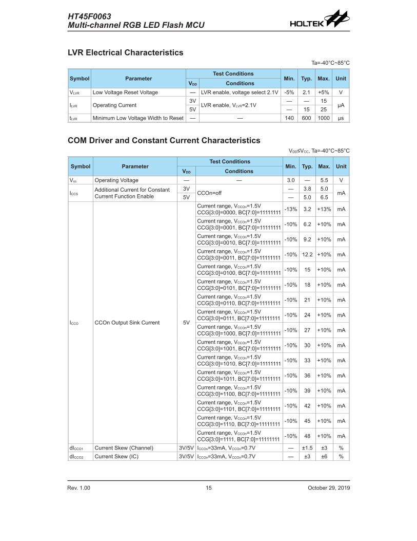
LVR Electrical CharacteristicsTa=-40°C~85°C
Symbol ParameterTest Conditions
Min. Typ. Max. UnitVDD Conditions
VLVR Low Voltage Reset Voltage — LVR enable, voltage select 2.1V -5% 2.1 +5% V
ILVR Operating Current3V
LVR enable, VLVR=2.1V— — 15
μA5V — 15 25
tLVR Minimum Low Voltage Width to Reset — — 140 600 1000 μs
COM Driver and Constant Current CharacteristicsVDD≤VCC, Ta=-40°C~85°C
Symbol ParameterTest Conditions
Min. Typ. Max. UnitVDD Conditions
Vcc Operating Voltage — — 3.0 — 5.5 V
ICCSAdditional Current for Constant Current Function Enable
3VCCOn=off
— 3.8 5.0mA
5V — 5.0 6.5
ICCO CCOn Output Sink Current 5V
Current range, VCCOn=1.5VCCG[3:0]=0000, BC[7:0]=11111111 -13% 3.2 +13% mA
Current range, VCCOn=1.5VCCG[3:0]=0001, BC[7:0]=11111111 -10% 6.2 +10% mA
Current range, VCCOn=1.5VCCG[3:0]=0010, BC[7:0]=11111111 -10% 9.2 +10% mA
Current range, VCCOn=1.5VCCG[3:0]=0011, BC[7:0]=11111111 -10% 12.2 +10% mA
Current range, VCCOn=1.5VCCG[3:0]=0100, BC[7:0]=11111111 -10% 15 +10% mA
Current range, VCCOn=1.5VCCG[3:0]=0101, BC[7:0]=11111111 -10% 18 +10% mA
Current range, VCCOn=1.5VCCG[3:0]=0110, BC[7:0]=11111111 -10% 21 +10% mA
Current range, VCCOn=1.5VCCG[3:0]=0111, BC[7:0]=11111111 -10% 24 +10% mA
Current range, VCCOn=1.5VCCG[3:0]=1000, BC[7:0]=11111111 -10% 27 +10% mA
Current range, VCCOn=1.5VCCG[3:0]=1001, BC[7:0]=11111111 -10% 30 +10% mA
Current range, VCCOn=1.5VCCG[3:0]=1010, BC[7:0]=11111111 -10% 33 +10% mA
Current range, VCCOn=1.5VCCG[3:0]=1011, BC[7:0]=11111111 -10% 36 +10% mA
Current range, VCCOn=1.5VCCG[3:0]=1100, BC[7:0]=11111111 -10% 39 +10% mA
Current range, VCCOn=1.5VCCG[3:0]=1101, BC[7:0]=11111111 -10% 42 +10% mA
Current range, VCCOn=1.5VCCG[3:0]=1110, BC[7:0]=11111111 -10% 45 +10% mA
Current range, VCCOn=1.5VCCG[3:0]=1111, BC[7:0]=11111111 -10% 48 +10% mA
dICCO1 Current Skew (Channel) 3V/5V ICCOn=33mA, VCCOn=0.7V — ±1.5 ±3 %dICCO2 Current Skew (IC) 3V/5V ICCOn=33mA, VCCOn=0.7V — ±3 ±6 %

Rev. 1.00 16 October 29, 2019 Rev. 1.00 17 October 29, 2019
HT45F0063Multi-channel RGB LED Flash MCU
HT45F0063Multi-channel RGB LED Flash MCU
Symbol ParameterTest Conditions
Min. Typ. Max. UnitVDD Conditions
RPH Pull-high Resistance for I/O Ports3V — 20 60 100
kΩ5V — 10 30 50
%/dVCCOOutput Current vs. Output Voltage Regulation 3V/5V VCCOn=0.7V~3.0V, ICCOn=33mA — ±0.1 — %/V
%/dVDDOutput Current vs. Supply Voltage Regulation — VDD=3.0V~5.5V, VCCOn=0.7V — ±1.0 ±8.0 %/V
ICOM_OH COM Driver Source Current 4.5V VOH=4V -364 -430 — mARCOM_PL COM Driver Pull-low Resistance 4.5V COMmOEN=1, COMm_data=0 6 10 18 kΩ
Note: 1. %/dVCCO={[ICCOn (at VCCOn=3.0V)-ICCOn (at VCCOn=0.7V)]/ICCOn (at VCCOn=1.5V)}×100%/(3.0V-0.7V).2. %/dVDD={[ICCOn (at VDD=5.5V)-ICCOn (at VDD=3.0V)]/ICCOn (at VDD=4.0V)}×100%/(5.5V-3.0V).3. The RCOM_PL internal pull low resistance value is calculated by connecting to VDD and set COMmOEN=1,
COMm_data=0, and then measuring the input current at the specified supply voltage level. Dividing the voltage by this measured current provides the RCOM_PL value.
Cascading Transceiver CharacteristicsTa=25°C
Symbol ParameterTest Conditions
Min. Typ. Max. UnitVDD Conditions
tCASDI CASDI Input Pin Minimum Pulse Width — — 0.3 — — μsfCASCLKI CASCLKI Maximum Clock Source Frequency 5V — — — 20 MHz
Power on Reset CharacteristicsTa=25°C
Symbol ParameterTest Conditions
Min. Typ. Max. UnitVDD Conditions
VPOR VDD Start Voltage to Ensure Power-on Reset — — — — 100 mVRRPOR VDD Rising Rate to Ensure Power-on Reset — — 0.035 — — V/ms
tPORMinimum Time for VDD Stays at VPOR to Ensure Power-on Reset — — 1 — — ms
VDD
tPOR RRPOR
VPOR
Time

Rev. 1.00 16 October 29, 2019 Rev. 1.00 17 October 29, 2019
HT45F0063Multi-channel RGB LED Flash MCU
HT45F0063Multi-channel RGB LED Flash MCU
System ArchitectureA key factor in the high-performance features of the Holtek range of microcontrollers is attributed to their internal system architecture. The device takes advantage of the usual features found within RISC microcontrollers providing increased speed of operation and enhanced performance. The pipelining scheme is implemented in such a way that instruction fetching and instruction execution are overlapped, hence instructions are effectively executed in one cycle, with the exception of branch or call instructions. An 8-bit wide ALU is used in practically all instruction set operations, which carries out arithmetic operations, logic operations, rotation, increment, decrement, branch decisions, etc. The internal data path is simplified by moving data through the Accumulator and the ALU. Certain internal registers are implemented in the Data Memory and can be directly or indirectly addressed. The simple addressing methods of these registers along with additional architectural features ensure that a minimum of external components is required to provide a functional I/O control system with maximum reliability and flexibility. This makes the device suitable for low-cost, high-volume production for controller applications.
Clocking and PipeliningThe main system clock, derived from either an HIRC or LIRC oscillator is subdivided into four internally generated non-overlapping clocks, T1~T4. The Program Counter is incremented at the beginning of the T1 clock during which time a new instruction is fetched. The remaining T2~T4 clocks carry out the decoding and execution functions. In this way, one T1~T4 clock cycle forms one instruction cycle. Although the fetching and execution of instructions takes place in consecutive instruction cycles, the pipelining structure of the microcontroller ensures that instructions are effectively executed in one instruction cycle. The exception to this are instructions where the contents of the Program Counter are changed, such as subroutine calls or jumps, in which case the instruction will take one more instruction cycle to execute.
For instructions involving branches, such as jump or call instructions, two machine cycles are required to complete instruction execution. An extra cycle is required as the program takes one cycle to first obtain the actual jump or call address and then another cycle to actually execute the branch. The requirement for this extra cycle should be taken into account by programmers in timing sensitive applications.
Fetch Inst. (PC)
(System Clock)fSYS
Phase Clock T1
Phase Clock T2
Phase Clock T3
Phase Clock T4
Program Counter PC PC+1 PC+2
PipeliningExecute Inst. (PC-1) Fetch Inst. (PC+1)
Execute Inst. (PC) Fetch Inst. (PC+2)
Execute Inst. (PC+1)
System Clocking and Pipelining

Rev. 1.00 18 October 29, 2019 Rev. 1.00 19 October 29, 2019
HT45F0063Multi-channel RGB LED Flash MCU
HT45F0063Multi-channel RGB LED Flash MCU
Fetch Inst. 11 MOV A,[12H]2 CALL DELAY3 CPL [12H]4 :5 :6 DELAY: NOP
Execute Inst. 1 Fetch Inst. 2 Execute Inst. 2
Fetch Inst. 3 Flush PipelineFetch Inst. 6 Execute Inst. 6
Fetch Inst. 7
Instruction Fetching
Program CounterDuring program execution, the Program Counter is used to keep track of the address of the next instruction to be executed. It is automatically incremented by one each time an instruction is executed except for instructions, such as “JMP” or “CALL” that demands a jump to a non-consecutive Program Memory address. Only the lower 8 bits, known as the Program Counter Low Register, are directly addressable by the application program.
When executing instructions requiring jumps to non-consecutive addresses such as a jump instruction, a subroutine call, interrupt or reset, etc., the microcontroller manages program control by loading the required address into the Program Counter. For conditional skip instructions, once the condition has been met, the next instruction, which has already been fetched during the present instruction execution, is discarded and a dummy cycle takes its place while the correct instruction is obtained.
Program CounterProgram Counter High Byte PCL Register
PC11~PC8 PCL7~PCL0
Program Counter
The lower byte of the Program Counter, known as the Program Counter Low register or PCL, is available for program control and is a readable and writeable register. By transferring data directly into this register, a short program jump can be executed directly. However, as only this low byte is available for manipulation, the jumps are limited to the present page of memory that is 256 locations. When such program jumps are executed it should also be noted that a dummy cycle will be inserted. Manipulating the PCL register may cause program branching, so an extra cycle is needed to pre-fetch.
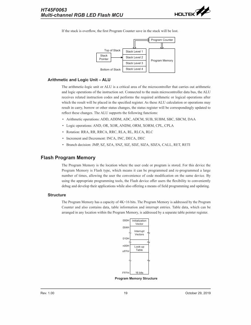
StackThis is a special part of the memory which is used to save the contents of the Program Counter only. The stack is organized into 4 levels and neither part of the data nor part of the program space, and is neither readable nor writeable. The activated level is indexed by the Stack Pointer, and is neither readable nor writeable. At a subroutine call or interrupt acknowledge signal, the contents of the Program Counter are pushed onto the stack. At the end of a subroutine or an interrupt routine, signaled by a return instruction, RET or RETI, the Program Counter is restored to its previous value from the stack. After a device reset, the Stack Pointer will point to the top of the stack.
If the stack is full and an enabled interrupt takes place, the interrupt request flag will be recorded but the acknowledge signal will be inhibited. When the Stack Pointer is decremented, by RET or RETI, the interrupt will be serviced. This feature prevents stack overflow allowing the programmer to use the structure more easily. However, when the stack is full, a CALL subroutine instruction can still be executed which will result in a stack overflow. Precautions should be taken to avoid such cases which might cause unpredictable program branching.
Rev. 1.00 18 October 29, 2019 Rev. 1.00 19 October 29, 2019
HT45F0063Multi-channel RGB LED Flash MCU
HT45F0063Multi-channel RGB LED Flash MCU
If the stack is overflow, the first Program Counter save in the stack will be lost.
StackPointer Stack Level 2
Stack Level 1
Stack Level 3
Stack Level 4
Program Memory
Program Counter
Bottom of Stack
Top of Stack
Arithmetic and Logic Unit – ALUThe arithmetic-logic unit or ALU is a critical area of the microcontroller that carries out arithmetic and logic operations of the instruction set. Connected to the main microcontroller data bus, the ALU receives related instruction codes and performs the required arithmetic or logical operations after which the result will be placed in the specified register. As these ALU calculation or operations may result in carry, borrow or other status changes, the status register will be correspondingly updated to reflect these changes. The ALU supports the following functions:
• Arithmetic operations: ADD, ADDM, ADC, ADCM, SUB, SUBM, SBC, SBCM, DAA
• Logic operations: AND, OR, XOR, ANDM, ORM, XORM, CPL, CPLA
• Rotation: RRA, RR, RRCA, RRC, RLA, RL, RLCA, RLC
• Increment and Decrement: INCA, INC, DECA, DEC
• Branch decision: JMP, SZ, SZA, SNZ, SIZ, SDZ, SIZA, SDZA, CALL, RET, RETI
Flash Program MemoryThe Program Memory is the location where the user code or program is stored. For this device the Program Memory is Flash type, which means it can be programmed and re-programmed a large number of times, allowing the user the convenience of code modification on the same device. By using the appropriate programming tools, the Flash device offer users the flexibility to conveniently debug and develop their applications while also offering a means of field programming and updating.
StructureThe Program Memory has a capacity of 4K×16 bits. The Program Memory is addressed by the Program Counter and also contains data, table information and interrupt entries. Table data, which can be arranged in any location within the Program Memory, is addressed by a separate table pointer register.
000H
004H
010H
FFFH
Initialization Vector
Interrupt Vectors
16 bits
Look-up Table
n00H
nFFH
Program Memory Structure
Rev. 1.00 20 October 29, 2019 Rev. 1.00 21 October 29, 2019
HT45F0063Multi-channel RGB LED Flash MCU
HT45F0063Multi-channel RGB LED Flash MCU
Special VectorsWithin the Program Memory, certain locations are reserved for the reset and interrupts. The location 000H is reserved for use by the device reset for program initialization. After a device reset is initiated, the program will jump to this location and begin execution.
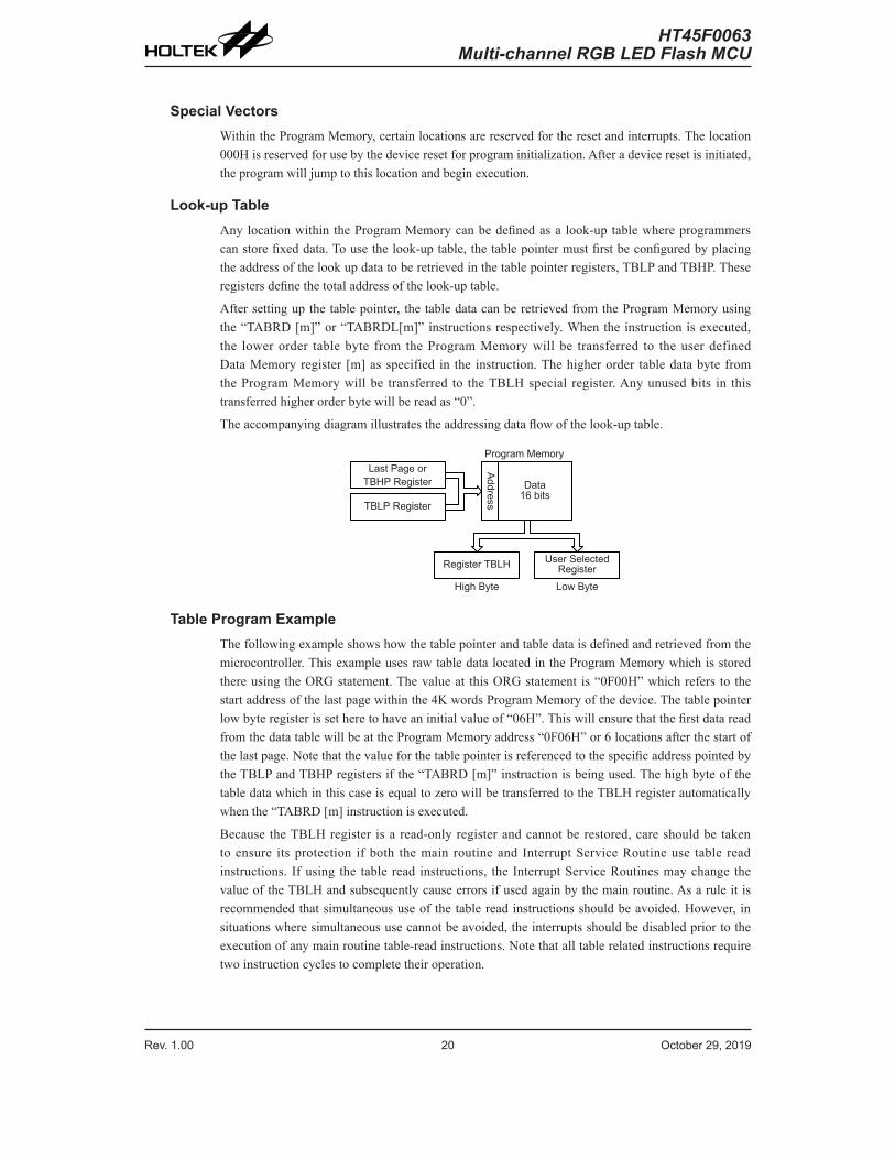
Look-up TableAny location within the Program Memory can be defined as a look-up table where programmers can store fixed data. To use the look-up table, the table pointer must first be configured by placing the address of the look up data to be retrieved in the table pointer registers, TBLP and TBHP. These registers define the total address of the look-up table.
After setting up the table pointer, the table data can be retrieved from the Program Memory using the “TABRD [m]” or “TABRDL[m]” instructions respectively. When the instruction is executed, the lower order table byte from the Program Memory will be transferred to the user defined Data Memory register [m] as specified in the instruction. The higher order table data byte from the Program Memory will be transferred to the TBLH special register. Any unused bits in this transferred higher order byte will be read as “0”.
The accompanying diagram illustrates the addressing data flow of the look-up table.
Last Page or TBHP Register
TBLP Register
Program Memory
Register TBLH User Selected Register
Address
Data16 bits
High Byte Low Byte
Table Program ExampleThe following example shows how the table pointer and table data is defined and retrieved from the microcontroller. This example uses raw table data located in the Program Memory which is stored there using the ORG statement. The value at this ORG statement is “0F00H” which refers to the start address of the last page within the 4K words Program Memory of the device. The table pointer low byte register is set here to have an initial value of “06H”. This will ensure that the first data read from the data table will be at the Program Memory address “0F06H” or 6 locations after the start of the last page. Note that the value for the table pointer is referenced to the specific address pointed by the TBLP and TBHP registers if the “TABRD [m]” instruction is being used. The high byte of the table data which in this case is equal to zero will be transferred to the TBLH register automatically when the “TABRD [m] instruction is executed.
Because the TBLH register is a read-only register and cannot be restored, care should be taken to ensure its protection if both the main routine and Interrupt Service Routine use table read instructions. If using the table read instructions, the Interrupt Service Routines may change the value of the TBLH and subsequently cause errors if used again by the main routine. As a rule it is recommended that simultaneous use of the table read instructions should be avoided. However, in situations where simultaneous use cannot be avoided, the interrupts should be disabled prior to the execution of any main routine table-read instructions. Note that all table related instructions require two instruction cycles to complete their operation.

Rev. 1.00 20 October 29, 2019 Rev. 1.00 21 October 29, 2019
HT45F0063Multi-channel RGB LED Flash MCU
HT45F0063Multi-channel RGB LED Flash MCU
Table Read Program Exampletempreg1 db? ; temporary register #1tempreg2 db? ; temporary register #2 : :mov a,06h ; initialize table pointer - note that this address is referencedmov tblp,a ; to the last page or the page that tbhp pointedmov a,0Fh ; initialize high table pointermov tbhp,a ; it is not necessary to set tbhp if executing tabrdl : :tabrd tempreg1 ; transfers value in table referenced by table pointer ; data at program memory address “F06H” transferred to tempreg1 and TBLHdec tblp ; reduce value of table pointer by onetabrd tempreg2 ; transfers value in table referenced by table pointer ; data at program memory address “F05H” transferred to tempreg2 and TBLH ; in this example the data “1AH” is transferred to tempreg1 and data “0FH” ; to tempreg2 ; the value “00H” will be transferred to the high byte register TBLH : :org 0F00h ; sets initial address of last pagedc 00Ah,00Bh,00Ch,00Dh,00Eh,00Fh,01Ah,01Bh
In Circuit Programming – ICPThe provision of Flash type Program Memory provides the user with a means of convenient and easy upgrades and modifications to their programs on the same device.
As an additional convenience, Holtek has provided a means of programming the microcontroller in-circuit using a 4-pin interface. This provides manufacturers with the possibility of manufacturing their circuit boards complete with a programmed or un-programmed microcontroller, and then programming or upgrading the program at a later stage. This enables product manufacturers to easily keep their manufactured products supplied with the latest program releases without removal and re-insertion of the device.
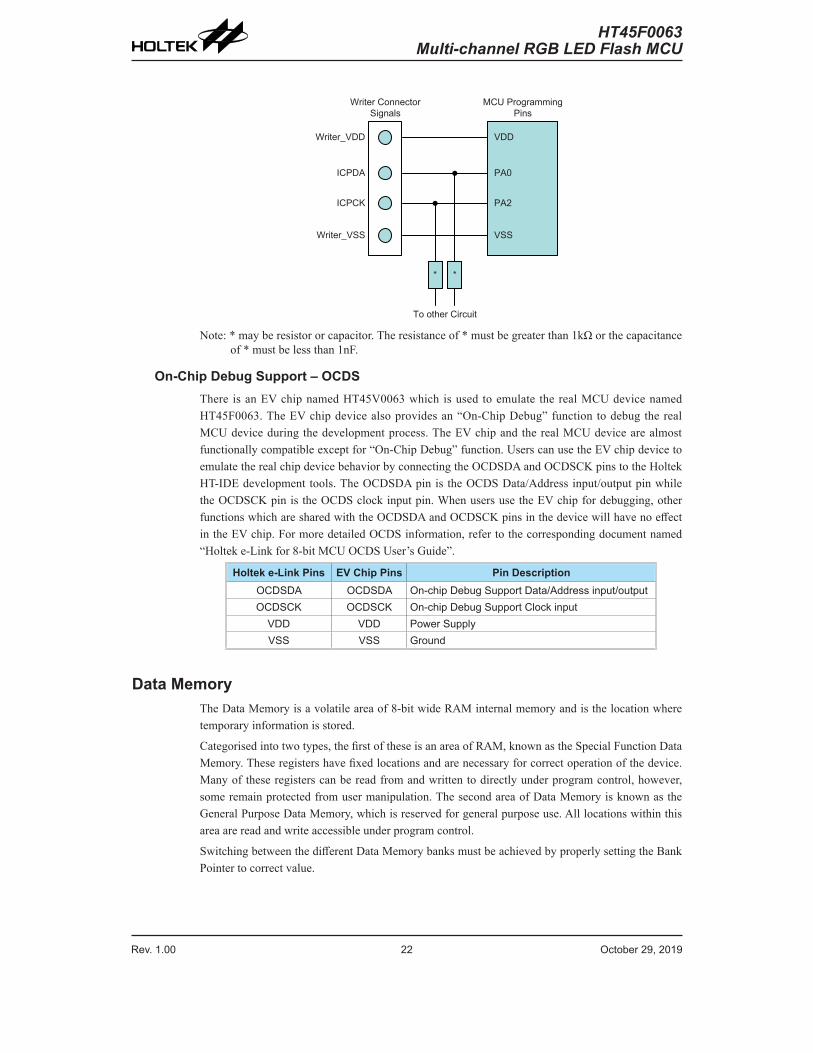
Holtek Writer Pins MCU Programming Pins Pin DescriptionICPDA PA0 Programming Serial Data/AddressICPCK PA2 Programming ClockVDD VDD Power SupplyVSS VSS Ground
The Program Memory can be programmed serially in-circuit using this 4-wire interface. Data is downloaded and uploaded serially on a single pin with an additional line for the clock. Two additional lines are required for the power supply. The technical details regarding the in-circuit programming of the device are beyond the scope of this document and will be supplied in supplementary literature.
During the programming process, the user can take care of the ICPDA and ICPCK pins for data and clock programming purposes to ensure that no other outputs are connected to these two pins.
Rev. 1.00 22 October 29, 2019 Rev. 1.00 23 October 29, 2019
HT45F0063Multi-channel RGB LED Flash MCU
HT45F0063Multi-channel RGB LED Flash MCU
* *
Writer_VDD
ICPDA
ICPCK
Writer_VSS
To other Circuit
VDD
PA0
PA2
VSS
Writer Connector Signals
MCU ProgrammingPins
Note: * may be resistor or capacitor. The resistance of * must be greater than 1kΩ or the capacitance of * must be less than 1nF.
On-Chip Debug Support – OCDSThere is an EV chip named HT45V0063 which is used to emulate the real MCU device named HT45F0063. The EV chip device also provides an “On-Chip Debug” function to debug the real MCU device during the development process. The EV chip and the real MCU device are almost functionally compatible except for “On-Chip Debug” function. Users can use the EV chip device to emulate the real chip device behavior by connecting the OCDSDA and OCDSCK pins to the Holtek HT-IDE development tools. The OCDSDA pin is the OCDS Data/Address input/output pin while the OCDSCK pin is the OCDS clock input pin. When users use the EV chip for debugging, other functions which are shared with the OCDSDA and OCDSCK pins in the device will have no effect in the EV chip. For more detailed OCDS information, refer to the corresponding document named “Holtek e-Link for 8-bit MCU OCDS User’s Guide”.
Holtek e-Link Pins EV Chip Pins Pin DescriptionOCDSDA OCDSDA On-chip Debug Support Data/Address input/outputOCDSCK OCDSCK On-chip Debug Support Clock input
VDD VDD Power SupplyVSS VSS Ground
Data MemoryThe Data Memory is a volatile area of 8-bit wide RAM internal memory and is the location where temporary information is stored.
Categorised into two types, the first of these is an area of RAM, known as the Special Function Data Memory. These registers have fixed locations and are necessary for correct operation of the device. Many of these registers can be read from and written to directly under program control, however, some remain protected from user manipulation. The second area of Data Memory is known as the General Purpose Data Memory, which is reserved for general purpose use. All locations within this area are read and write accessible under program control.
Switching between the different Data Memory banks must be achieved by properly setting the Bank Pointer to correct value.

Rev. 1.00 22 October 29, 2019 Rev. 1.00 23 October 29, 2019
HT45F0063Multi-channel RGB LED Flash MCU
HT45F0063Multi-channel RGB LED Flash MCU
StructureThe Data Memory is subdivided into three banks, which are implemented in 8-bit wide Memory. The Data Memory Bank is categorized into two types, the special Purpose Data Memory and the General Purpose Data Memory. The address range of the Special Purpose Data Memory for the device is from 00H to 7FH while the General Purpose Data Memory address range is from 80H to FFH. Data Memory addresses from 80H to FFH in Bank 2 are used as the LED PWM data buffer.
Special PurposeData Memory
General PurposeData Memory
LED PWMData Memory
Located Bank Capacity Bank: Address Capacity Bank: Address
0 256×8 0, 1: 80H~FFH 128×8Buffer_A 2: 80H~BFHBuffer_B 2: C0H~FFH
Data Memory Summary
00H
7FH80H
FFH
Special Purpose Data Memory
General Purpose Data Memory
Bank 0Bank 1
LED PWM Data Memory
Bank 2
Data Memory Structure
General Purpose Data MemoryAll microcontroller programs require an area of read/write memory where temporary data can be stored and retrieved for use later. It is this area of RAM memory that is known as General Purpose Data Memory. This area of Data Memory is fully accessible by the user programing for both reading and writing operations. By using the bit operation instructions individual bits can be set or reset under program control giving the user a large range of flexibility for bit manipulation in the Data Memory.
Special Purpose Data MemoryThis area of Data Memory is where registers, necessary for the correct operation of the microcontroller, are stored. Most of the registers are both readable and writeable but some are protected and are readable only, the details of which are located under the relevant Special Function Register section. Note that for locations that are unused, any read instruction to these addresses will return the value “00H”.

Rev. 1.00 24 October 29, 2019 Rev. 1.00 25 October 29, 2019
HT45F0063Multi-channel RGB LED Flash MCU
HT45F0063Multi-channel RGB LED Flash MCU
: Unused, read as 00H
PWM9DATAPWM8DATAPWM7DATAPWM6DATAPWM5DATAPWM4DATAPWM3DATAPWM2DATAPWM1DATAPWM0DATACOM_PWM
CTMAHCTMALCTMDHCTMDLCTMC1CTMC0
PBS1PBS0PAS1PAS0TBC
PSCRPBPUPBCPB
PAWUPAPUPACPA
MFIINTC1INTC0RSTFCWDTCHIRCCSCC
STATUSTBHPTBLHTBLPPCLACCBP
MP1IAR1MP0IAR0
PWM14DATAPWM13DATAPWM12DATAPWM11DATAPWM10DATA
CCOPU1CCOPU0IICTOC
IICAIICD
IICC1IICC0CCS
INTCON1INTCON0
CASD35CASD34CASD33CASD32CASD31CASD30CASD29CASD28CASD27CASD26CASD25CASD24CASD23CASD22CASD21CASD20CASD19CASD18CASD17CASD16CASD15CASD14CASD13CASD12CASD11CASD10CASD9CASD8CASD7CASD6CASD5CASD4CASD3CASD240H
41H42H43H44H45H46H47H48H49H4AH4BH4CH4DH4EH4FH50H51H52H
59H58H
5BH5AH
5DH5CH
5FH
53H54H55H56H57H
5EH
60H61H62H
69H68H
6BH6AH
6DH6CH
63H64H65H66H67H
7FH
Bank 0 Bank 000H01H02H03H04H05H06H07H08H09H0AH0BH0CH0DH0EH0FH10H11H12H
19H18H
1BH1AH
1DH1CH
1FH
13H14H15H16H17H
1EH
20H21H22H
29H28H
2BH2AH
2DH2CH
2FH2EH
23H24H25H26H27H
30H31H32H
38H
3CH
33H34H35H36H37H
3BH
39H3AH
3DH
3FH3EH
PCS0IFS
CASTHCASPRECASCON
BCLVRCPCPUPCCPC
CASD1CASD0
CASDNBRCNTPCNT
D1CNTD0CNT
CASD47CASD46CASD45CASD44CASD43CASD42CASD41CASD40CASD39CASD38CASD37CASD36
74H73H
76H75H
78H77H
6EH6FH70H71H72H
7DH7CH
7EH
79H7AH7BH
Special Purpose Data Memory

Rev. 1.00 24 October 29, 2019 Rev. 1.00 25 October 29, 2019
HT45F0063Multi-channel RGB LED Flash MCU
HT45F0063Multi-channel RGB LED Flash MCU
Special Function Register DescriptionMost of the Special Function Register details will be described in the relevant functional section, however several registers require a separate description in this section.
Indirect Addressing Registers – IAR0, IAR1The Indirect Addressing Registers, IAR0 and IAR1, although having their locations in normal RAM register space, do not actually physically exist as normal registers. The method of indirect addressing for RAM data manipulation uses these Indirect Addressing Registers and Memory Pointers, in contrast to direct memory addressing, where the actual memory address is specified. Actions on the IAR0 and IAR1 registers will result in no actual read or write operation to these registers but rather to the memory location specified by their corresponding Memory Pointers, MP0 or MP1. Acting as a pair, IAR0 and MP0 can together access data from Bank 0 while the IAR1 register together with the MP1 register can access data from any Data Memory Bank. As the Indirect Addressing Registers are not physically implemented, reading the Indirect Addressing Registers will return a result of “00H” and writing to the registers will result in no operation.
Memory Pointers – MP0, MP1Two Memory Pointers, known as MP0 and MP1 are provided. These Memory Pointers are physically implemented in the Data Memory and can be manipulated in the same way as normal registers providing a convenient way with which to address and track data. When any operation to the relevant Indirect Addressing Registers is carried out, the actual address that the microcontroller is directed to is the address specified by the related Memory Pointer. MP0, together with Indirect Addressing Register, IAR0, are used to access data from Bank 0, while MP1 together with IAR1 are used to access data from all banks according to the desired data memory bank selected by the DMBP1~DMBP0 bits in the BP register. Direct Addressing can only be used with Bank 0, Bank 1 and Bank 2 must be addressed indirectly using MP1 and IAR1.
The following example shows how to clear a section of four Data Memory locations already defined as locations adres1 to adres4.
Indirect Addressing Program Exampledata .section ´data´adres1 db ?adres2 db ?adres3 db ?adres4 db ?block db ?code .section at 0 code´org 00hstart: mov a,04h ; set size of block mov block,a mova,offsetadres1 ;AccumulatorloadedwithfirstRAMaddress movmp0,a ;setmemorypointerwithfirstRAMaddressloop; clrIAR0 ;clearthedataataddressdefinedbymp0 inc mp0 ; increment memory pointer sdz block ; check if last memory location has been cleared jmp loopcontinue;
The important point to note here is that in the example shown above, no reference is made to specific Data Memory addresses.
Rev. 1.00 26 October 29, 2019 Rev. 1.00 27 October 29, 2019
HT45F0063Multi-channel RGB LED Flash MCU
HT45F0063Multi-channel RGB LED Flash MCU
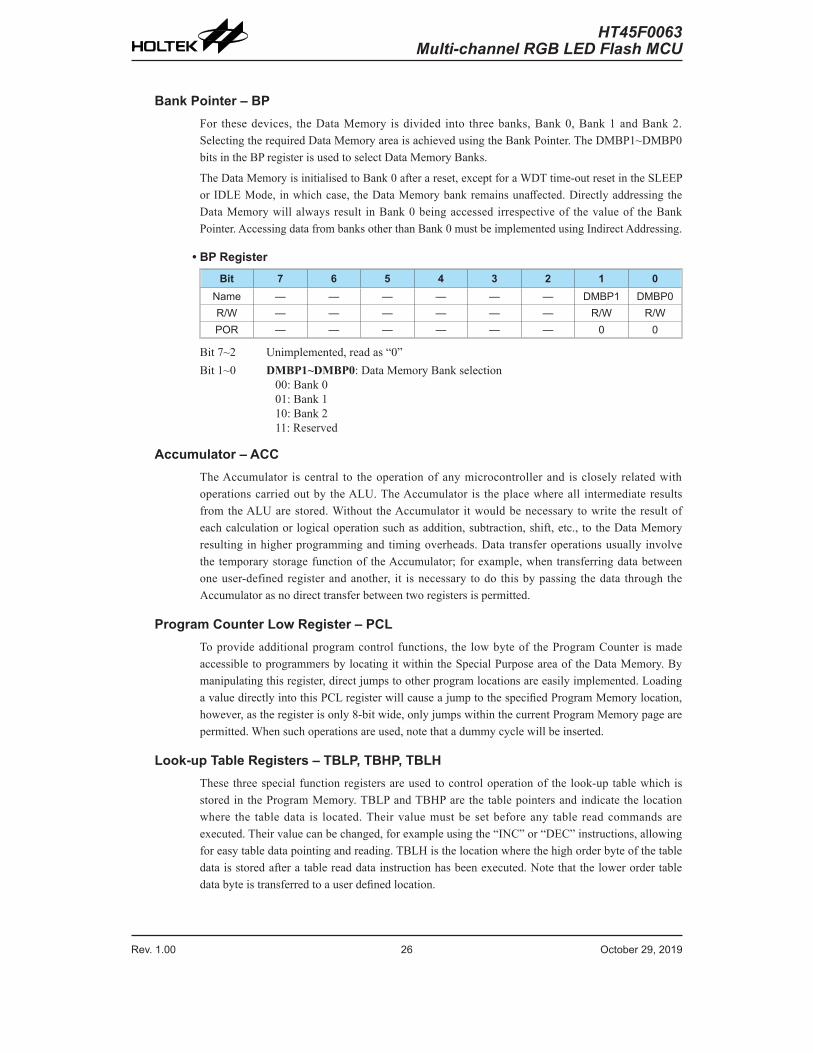
Bank Pointer – BPFor these devices, the Data Memory is divided into three banks, Bank 0, Bank 1 and Bank 2. Selecting the required Data Memory area is achieved using the Bank Pointer. The DMBP1~DMBP0 bits in the BP register is used to select Data Memory Banks.
The Data Memory is initialised to Bank 0 after a reset, except for a WDT time-out reset in the SLEEP or IDLE Mode, in which case, the Data Memory bank remains unaffected. Directly addressing the Data Memory will always result in Bank 0 being accessed irrespective of the value of the Bank Pointer. Accessing data from banks other than Bank 0 must be implemented using Indirect Addressing.
• BP RegisterBit 7 6 5 4 3 2 1 0
Name — — — — — — DMBP1 DMBP0R/W — — — — — — R/W R/WPOR — — — — — — 0 0
Bit 7~2 Unimplemented, read as “0”Bit 1~0 DMBP1~DMBP0: Data Memory Bank selection
00: Bank 001: Bank 110: Bank 211: Reserved
Accumulator – ACCThe Accumulator is central to the operation of any microcontroller and is closely related with operations carried out by the ALU. The Accumulator is the place where all intermediate results from the ALU are stored. Without the Accumulator it would be necessary to write the result of each calculation or logical operation such as addition, subtraction, shift, etc., to the Data Memory resulting in higher programming and timing overheads. Data transfer operations usually involve the temporary storage function of the Accumulator; for example, when transferring data between one user-defined register and another, it is necessary to do this by passing the data through the Accumulator as no direct transfer between two registers is permitted.
Program Counter Low Register – PCLTo provide additional program control functions, the low byte of the Program Counter is made accessible to programmers by locating it within the Special Purpose area of the Data Memory. By manipulating this register, direct jumps to other program locations are easily implemented. Loading a value directly into this PCL register will cause a jump to the specified Program Memory location, however, as the register is only 8-bit wide, only jumps within the current Program Memory page are permitted. When such operations are used, note that a dummy cycle will be inserted.
Look-up Table Registers – TBLP, TBHP, TBLHThese three special function registers are used to control operation of the look-up table which is stored in the Program Memory. TBLP and TBHP are the table pointers and indicate the location where the table data is located. Their value must be set before any table read commands are executed. Their value can be changed, for example using the “INC” or “DEC” instructions, allowing for easy table data pointing and reading. TBLH is the location where the high order byte of the table data is stored after a table read data instruction has been executed. Note that the lower order table data byte is transferred to a user defined location.

Rev. 1.00 26 October 29, 2019 Rev. 1.00 27 October 29, 2019
HT45F0063Multi-channel RGB LED Flash MCU
HT45F0063Multi-channel RGB LED Flash MCU
Status Register – STATUSThis 8-bit register contains the zero flag (Z), carry flag (C), auxiliary carry flag (AC), overflow flag (OV), power down flag (PDF), and watchdog time-out flag (TO). These arithmetic/logical operation and system management flags are used to record the status and operation of the microcontroller.
With the exception of the TO and PDF flags, bits in the status register can be altered by instructions like most other registers. Any data written into the status register will not change the TO or PDF flag. In addition, operations related to the status register may give different results due to the different instruction operations. The TO flag can be affected only by a system power-up, a WDT time-out or by executing the “CLR WDT” or “HALT” instruction. The PDF flag is affected only by executing the “HALT” or “CLR WDT” instruction or during a system power-up.
The Z, OV, AC, and C flags generally reflect the status of the latest operations.
• C is set if an operation results in a carry during an addition operation or if a borrow does not take place during a subtraction operation; otherwise C is cleared. C is also affected by a rotate through carry instruction.
• AC is set if an operation results in a carry out of the low nibbles in addition, or no borrow from the high nibble into the low nibble in subtraction; otherwise AC is cleared.
• Z is set if the result of an arithmetic or logical operation is zero; otherwise Z is cleared.
• OV is set if an operation results in a carry into the highest-order bit but not a carry out of the highest-order bit, or vice versa; otherwise OV is cleared.
• PDF is cleared by a system power-up or executing the “CLR WDT” instruction. PDF is set by executing the “HALT” instruction.
• TO is cleared by a system power-up or executing the “CLR WDT” or “HALT” instruction. TO is set by a WDT time-out.
In addition, on entering an interrupt sequence or executing a subroutine call, the status register will not be pushed onto the stack automatically. If the contents of the status registers are important and if the subroutine can corrupt the status register, precautions must be taken to correctly save it.
• STATUS RegisterBit 7 6 5 4 3 2 1 0
Name — — TO PDF OV Z AC CR/W — — R R R/W R/W R/W R/WPOR — — 0 0 x x x x
“x”: unknownBit 7~6 Unimplemented, read as “0”Bit 5 TO: Watchdog Time-Out flag
0: After power up or executing the “CLR WDT” or “HALT” instruction1: A watchdog time-out occurred.
Bit 4 PDF: Power down flag0: After power up or executing the “CLR WDT” instruction1: By executing the “HALT” instruction
Bit 3 OV: Overflow flag0: No overflow1: An operation results in a carry into the highest-order bit but not a carry out of the
highest-order bit or vice versa.Bit 2 Z: Zero flag
0: The result of an arithmetic or logical operation is not zero1: The result of an arithmetic or logical operation is zero
Rev. 1.00 28 October 29, 2019 Rev. 1.00 29 October 29, 2019
HT45F0063Multi-channel RGB LED Flash MCU
HT45F0063Multi-channel RGB LED Flash MCU
Bit 1 AC: Auxiliary flag0: No auxiliary carry1: An operation results in a carry out of the low nibbles in addition, or no borrow
from the high nibble into the low nibble in subtractionBit 0 C: Carry flag
0: No carry-out1: An operation results in a carry during an addition operation or if a borrow does
not take place during a subtraction operationThe C flag is also affected by a rotate through carry instruction.
OscillatorsVarious oscillator options offer the user a wide range of functions according to their various application requirements. The flexible features of the oscillator functions ensure that the best optimisation can be achieved in terms of speed and power saving. Oscillator operations are selected through the application program and relevant control registers.
Oscillator OverviewIn addition to being the source of the main system clock the oscillators also provide clock sources for the Watchdog Timer and Time Base Interrupts. Two fully integrated internal oscillators, requiring no external components, are provided to form a range of both fast and slow system oscillators. The higher frequency oscillator provides higher performance but carry with it the disadvantage of higher power requirements, while the opposite is of course true for the lower frequency oscillator. With the capability of dynamically switching between fast and slow system clock, the device has the flexibility to optimize the performance/power ratio, a feature especially important in power sensitive portable applications.
Type Name FrequencyInternal High Speed RC HIRC 8MHzInternal Low Speed RC LIRC 32kHz
Oscillator Types
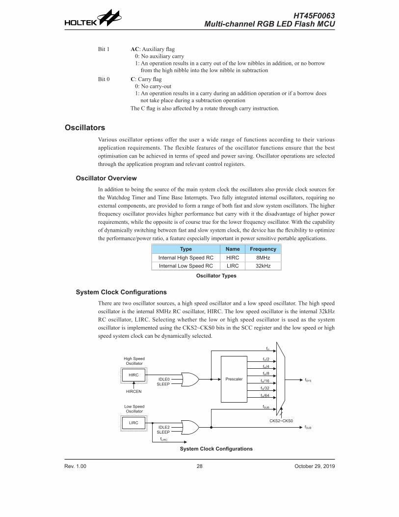
System Clock ConfigurationsThere are two oscillator sources, a high speed oscillator and a low speed oscillator. The high speed oscillator is the internal 8MHz RC oscillator, HIRC. The low speed oscillator is the internal 32kHz RC oscillator, LIRC. Selecting whether the low or high speed oscillator is used as the system oscillator is implemented using the CKS2~CKS0 bits in the SCC register and the low speed or high speed system clock can be dynamically selected.
High Speed Oscillator
PrescalerHIRC
fH/2
fH/4
fH/8
fH/16
fH/32
fH/64
CKS2~CKS0
fSYS
Low Speed Oscillator
LIRC
IDLE0SLEEP
IDLE2SLEEP
fSUB
fSUB
fLIRC
HIRCEN
fH
System Clock Configurations
Rev. 1.00 28 October 29, 2019 Rev. 1.00 29 October 29, 2019
HT45F0063Multi-channel RGB LED Flash MCU
HT45F0063Multi-channel RGB LED Flash MCU
High Speed Internal RC Oscillator – HIRCThe high speed internal RC oscillator is a fully integrated system oscillator requiring no external components. The internal RC oscillator has a fixed frequency of 8MHz. Device trimming during the manufacturing process and the inclusion of internal frequency compensation circuits are used to ensure that the influence of the power supply voltage, temperature and process variations on the oscillation frequency are minimised. This internal system clock requires no external pins for its operation.
Internal 32kHz Oscillator – LIRCThe internal 32kHz System Oscillator is a fully integrated RC oscillator with a typical frequency of 32kHz, requiring no external components for its implementation. Device trimming during the manufacturing process and the inclusion of internal frequency compensation circuits are used to ensure that the influence of the power supply voltage, temperature and process variations on the oscillation frequency are minimised.
Operating Modes and System ClocksPresent day applications require that their microcontrollers have high performance but often still demand that they consume as little power as possible, conflicting requirements that are especially true in battery powered portable applications. The fast clocks required for high performance will by their nature increase current consumption and of course vice-versa, lower speed clocks reduce current consumption. As Holtek has provided the device with both high and low speed clock sources and the means to switch between them dynamically, the user can optimise the operation of their microcontroller to achieve the best performance/power ratio.
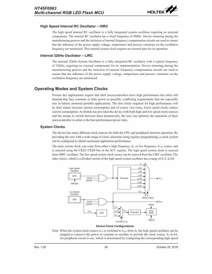
System ClocksThe device has many different clock sources for both the CPU and peripheral function operation. By providing the user with a wide range of clock selections using register programming, a clock system can be configured to obtain maximum application performance.The main system clock, can come from either a high frequency, fH, or low frequency, fSUB, source, and is selected using the CKS2~CKS0 bits in the SCC register. The high speed system clock is sourced from HIRC oscillator. The low speed system clock source can be sourced from the LIRC oscillator. The other choice, which is a divided version of the high speed system oscillator has a range of fH/2~fH/64.
High Speed Oscillator
PrescalerHIRC
fH/2
fH/4
fH/8
fH/16
fH/32
fH/64
CKS2~CKS0
fSYS
Low Speed Oscillator
LIRC
IDLE0SLEEP
IDLE2SLEEP
fSUB
fSUB
fLIRC
HIRCEN
fH
fSUB
fSYS/4
fSYS
CLKSEL[1:0]
fPSCPrescaler
TimeBase
TBON
TB[2:0]
WDT
Device Clock ConfigurationsNote: When the system clock source fSYS is switched to fSUB from fH, the high speed oscillator can be
stopped to conserve the power or continue to oscillate to provide the clock source, fH~fH/64, for peripheral circuit to use, which is determined by configuring the corresponding high speed

Rev. 1.00 30 October 29, 2019 Rev. 1.00 31 October 29, 2019
HT45F0063Multi-channel RGB LED Flash MCU
HT45F0063Multi-channel RGB LED Flash MCU
oscillator enable control bit.
System Operation ModesThere are six different modes of operation for the microcontroller, each one with its own special characteristics and which can be chosen according to the specific performance and power requirements of the application. There are two modes allowing normal operation of the microcontroller, the FAST Mode and SLOW Mode. The remaining four modes, the SLEEP, IDLE0, IDLE1 and IDLE2 Mode are used when the microcontroller CPU is switched off to conserve power.
Operation Mode CPU
Register SettingfSYS fH fSUB fLIRC
FHIDEN FSIDEN CKS2~CKS0FAST Mode On x x 000~110 fH~fH/64 On On OnSLOW Mode On x x 111 fSUB On/Off(1) On On
IDLE0 Mode Off 0 1000~110 Off
Off On On111 On
IDLE1 Mode Off 1 1 xxx On On On On
IDLE2 Mode Off 1 0000~110 On
On Off On111 Off
SLEEP Mode Off 0 0 xxx Off Off Off On/Off(2)
“x”: Don’t careNote: 1. The fH clock will be switched on or off by configuring the corresponding oscillator enable bit
in the SLOW mode.2. The fLIRC clock can be switched on or off which is controlled by the WDT function being
enabled or disabled in the SLEEP mode.
FAST ModeThis is one of the main operating modes where the microcontroller has all of its functions operational and where the system clock is provided by the high speed oscillator. This mode operates allowing the microcontroller to operate normally with a clock source will come from the high speed oscillator, HIRC. The high speed oscillator will however first be divided by a ratio ranging from 1 to 64, the actual ratio being selected by the CKS2~CKS0 bits in the SCC register. Although a high speed oscillator is used, running the microcontroller at a divided clock ratio reduces the operating current.
SLOW ModeThis is also a mode where the microcontroller operates normally although now with a slower speed clock source. The clock source used will be from fSUB. The fSUB clock is derived from the LIRC oscillator.
SLEEP ModeThe SLEEP Mode is entered when a HALT instruction is executed and when the FHIDEN and FSIDEN bit are low. In the SLEEP mode the CPU will be stopped. The fSUB clock provided to the peripheral function will also be stopped, too. However the fLIRC clock can still continue to operate if the WDT function is enabled by the WDTC register.
IDLE0 Mode The IDLE0 Mode is entered when a HALT instruction is executed and when the FHIDEN bit in the SCC register is low and the FSIDEN bit in the SCC register is high. In the IDLE0 Mode the CPU will be switched off but the low speed oscillator will be turned on to drive some peripheral functions.
IDLE1 ModeThe IDLE1 Mode is entered when a HALT instruction is executed and when the FHIDEN bit in the SCC register is high and the FSIDEN bit in the SCC register is high. In the IDLE1 Mode the CPU

Rev. 1.00 30 October 29, 2019 Rev. 1.00 31 October 29, 2019
HT45F0063Multi-channel RGB LED Flash MCU
HT45F0063Multi-channel RGB LED Flash MCU
will be switched off but both the high and low speed oscillators will be turned on to provide a clock source to keep some peripheral functions operational.
IDLE2 ModeThe IDLE2 Mode is entered when a HALT instruction is executed and when the FHIDEN bit in the SCC register is high and the FSIDEN bit in the SCC register is low. In the IDLE2 Mode the CPU will be switched off but the high speed oscillator will be turned on to provide a clock source to keep some peripheral functions operational.
Control RegisterThe SCC and HIRCC registers are used to control the system clock and the corresponding oscillator configurations.
Register Name
Bit7 6 5 4 3 2 1 0
SCC CKS2 CKS1 CKS0 — — — FHIDEN FSIDENHIRCC — — — — — — HIRCF HIRCEN
System Operating Mode Control Register List
• SCC RegisterBit 7 6 5 4 3 2 1 0
Name CKS2 CKS1 CKS0 — — — FHIDEN FSIDENR/W R/W R/W R/W — — — R/W R/WPOR 0 0 0 — — — 0 0
Bit 7~5 CKS2~CKS0: System clock selection000: fH
001: fH/2010: fH/4011: fH/8100: fH/16101: fH/32110: fH/64111: fSUB
These three bits are used to select which clock is used as the system clock source. In addition to the system clock source directly derived from fH or fSUB, a divided version of the high speed system oscillator can also be chosen as the system clock source.
Bit 4~2 Unimplemented, read as “0”Bit 1 FHIDEN: High Frequency oscillator control when CPU is switched off
0: Disable1: Enable
This bit is used to control whether the high speed oscillator is activated or stopped when the CPU is switched off by executing a “HALT” instruction.
Bit 0 FSIDEN: Low Frequency oscillator control when CPU is switched off0: Disable1: Enable
This bit is used to control whether the low speed oscillator is activated or stopped when the CPU is switched off by executing a “HALT” instruction.

Rev. 1.00 32 October 29, 2019 Rev. 1.00 33 October 29, 2019
HT45F0063Multi-channel RGB LED Flash MCU
HT45F0063Multi-channel RGB LED Flash MCU
• HIRCC RegisterBit 7 6 5 4 3 2 1 0
Name — — — — — — HIRCF HIRCENR/W — — — — — — R R/WPOR — — — — — — 0 1
Bit 7~2 Unimplemented, read as “0”Bit 1 HIRCF: HIRC oscillator stable flag
0: Unstable1: Stable
This bit is used to indicate whether the HIRC oscillator is stable or not. When the HIRCEN bit is set to 1 to enable the HIRC oscillator, the HIRCF bit will first be cleared to 0 and then set to 1 after the HIRC oscillator is stable.
Bit 0 HIRCEN: HIRC oscillator enable control0: Disable1: Enable
Operating Mode Switching The device can switch between operating modes dynamically allowing the user to select the best performance/power ratio for the present task in hand. In this way microcontroller operations that do not require high performance can be executed using slower clocks thus requiring less operating current and prolonging battery life in portable applications.
In simple terms, mode switching between the FAST Mode and SLOW Mode is executed using the CKS2~CKS0 bits in the SCC register while mode switching from the FAST/SLOW Modes to the SLEEP/IDLE Modes is executed via the a HALT instruction. When a HALT instruction is executed, whether the device enters the IDLE Mode or the SLEEP Mode is determined by the condition of the FHIDEN and FSIDEN bits in the SCC register.
FASTfSYS=fH~fH/64
fH onCPU runfSYS onfSUB on
SLOWfSYS=fSUBfSUB on
CPU runfSYS onfH on/off
IDLE0HALT instruction executed
CPU stopFHIDEN=0FSIDEN=1
fH offfSUB on
IDLE1HALT instruction executed
CPU stopFHIDEN=1FSIDEN=1
fH onfSUB on
IDLE2HALT instruction executed
CPU stopFHIDEN=1FSIDEN=0
fH onfSUB off
SLEEPHALT instruction executed
CPU stopFHIDEN=0FSIDEN=0
fH offfSUB off

Rev. 1.00 32 October 29, 2019 Rev. 1.00 33 October 29, 2019
HT45F0063Multi-channel RGB LED Flash MCU
HT45F0063Multi-channel RGB LED Flash MCU
FAST Mode to SLOW Mode Switching When running in the FAST Mode, which uses the high speed system oscillator, and therefore consumes more power, the system clock can switch to run in the SLOW Mode by setting the CKS2~CKS0 bits to “111” in the SCC register. This will then use the low speed system oscillator which will consume less power. Users may decide to do this for certain operations which do not require high performance and can subsequently reduce power consumption.
The SLOW Mode system clock is sourced from the LIRC oscillator and therefore requires this oscillator to be stable before full mode switching occurs.
FAST Mode
SLOW Mode
CKS2~CKS0=111
SLEEP Mode
FHIDEN=0, FSIDEN=0HALT instruction is executed
IDLE0 Mode
FHIDEN=0, FSIDEN=1HALT instruction is executed
IDLE1 Mode
FHIDEN=1, FSIDEN=1HALT instruction is executed
IDLE2 Mode
FHIDEN=1, FSIDEN=0HALT instruction is executed

Rev. 1.00 34 October 29, 2019 Rev. 1.00 35 October 29, 2019
HT45F0063Multi-channel RGB LED Flash MCU
HT45F0063Multi-channel RGB LED Flash MCU
SLOW Mode to FAST Mode SwitchingIn SLOW mode the system clock is derived from fSUB. When system clock is switched back to the FAST mode from fSUB, the CKS2~CKS0 bits should be set to “000”~“110” and then the system clock will respectively be switched to fH~fH/64.
However, if fH is not used in SLOW mode and thus switched off, it will take some time to re-oscillate and stabilise when switching to the FAST mode from the SLOW Mode. This is monitored using the HIRCF bit in the HIRCC register. The time duration required for the high speed system oscillator stabilization is specified in the System Start Up Time Characteristics.
FAST Mode
SLOW Mode
CKS2~CKS0=000~110
SLEEP Mode
FHIDEN=0, FSIDEN=0HALT instruction is executed
IDLE0 Mode
FHIDEN=0, FSIDEN=1HALT instruction is executed
IDLE1 Mode
FHIDEN=1, FSIDEN=1HALT instruction is executed
IDLE2 Mode
FHIDEN=1, FSIDEN=0HALT instruction is executed
Entering the SLEEP ModeThere is only one way for the device to enter the SLEEP Mode and that is to execute the “HALT” instruction in the application program with both the FHIDEN and FSIDEN bits in the SCC register equal to “0”. When this instruction is executed under the conditions described above, the following will occur:
• The system clock will be stopped and the application program will stop at the “HALT” instruction.
• The Data Memory contents and registers will maintain their present condition.
• The I/O ports will maintain their present conditions.
• In the status register, the Power Down flag, PDF, will be set and the Watchdog time-out flag, TO, will be cleared.
• The WDT will be cleared and resume counting if the WDT function is enabled. If the WDT function is disabled, the WDT will be cleared and then stopped.

Rev. 1.00 34 October 29, 2019 Rev. 1.00 35 October 29, 2019
HT45F0063Multi-channel RGB LED Flash MCU
HT45F0063Multi-channel RGB LED Flash MCU
Entering the IDLE0 Mode There is only one way for the device to enter the IDLE0 Mode and that is to execute the “HALT” instruction in the application program with the FHIDEN bit in the SCC register equal to “0” and the FSIDEN bit in the SCC register equal to “1”. When this instruction is executed under the conditions described above, the following will occur:
• The fH clock will be stopped and the application program will stop at the “HALT” instruction, but the fSUB clock will be on.
• The Data Memory contents and registers will maintain their present condition.
• The I/O ports will maintain their present conditions.
• In the status register, the Power Down flag, PDF, will be set and the Watchdog time-out flag, TO, will be cleared.
• The WDT will be cleared and resume counting if the WDT function is enabled. If the WDT function is disabled, the WDT will be cleared and then stopped.
Entering the IDLE1 Mode There is only one way for the device to enter the IDLE1 Mode and that is to execute the “HALT” instruction in the application program with both the FHIDEN and FSIDEN bits in the SCC register equal to “1”. When this instruction is executed under the conditions described above, the following will occur:
• The fH and fSUB clocks will be on but the application program will stop at the “HALT” instruction.
• The Data Memory contents and registers will maintain their present condition.
• The I/O ports will maintain their present conditions.
• In the status register, the Power Down flag, PDF, will be set and the Watchdog time-out flag, TO, will be cleared.
• The WDT will be cleared and resume counting if the WDT function is enabled. If the WDT function is disabled, the WDT will be cleared and then stopped.
Entering the IDLE2 Mode There is only one way for the device to enter the IDLE2 Mode and that is to execute the “HALT” instruction in the application program with the FHIDEN bit in the SCC register equal to “1” and the FSIDEN bit in SCC register equal to “0”. When this instruction is executed under the conditions described above, the following will occur:
• The fH clock will be on but the fSUB clock will be off and the application program will stop at the “HALT” instruction.
• The Data Memory contents and registers will maintain their present condition.
• The I/O ports will maintain their present conditions.
• In the status register, the Power Down flag, PDF, will be set and the Watchdog time-out flag, TO, will be cleared.
• The WDT will be cleared and resume counting if the WDT function is enabled. If the WDT function is disabled, the WDT will be cleared and then stopped.

Rev. 1.00 36 October 29, 2019 Rev. 1.00 37 October 29, 2019
HT45F0063Multi-channel RGB LED Flash MCU
HT45F0063Multi-channel RGB LED Flash MCU
Standby Current ConsiderationsAs the main reason for entering the SLEEP or IDLE Mode is to keep the current consumption of the device to as low a value as possible, perhaps only in the order of several micro-amps except in the IDLE1 and IDLE2 Mode, there are other considerations which must also be taken into account by the circuit designer if the power consumption is to be minimised. Special attention must be made to the I/O pins on the device. All high-impedance input pins must be connected to either a fixed high or low level as any floating input pins could create internal oscillations and result in increased current consumption. These must either be set as outputs or if set as inputs must have pull-high resistors connected.
Care must also be taken with the loads, which are connected to I/O pins, which are set as outputs. These should be placed in a condition in which minimum current is drawn or connected only to external circuits that do not draw current, such as other CMOS inputs. Also note that additional standby current will also be required if the LIRC oscillator has enabled.
In the IDLE1 and IDLE2 Mode the high speed oscillator is on, if the peripheral function clock source is derived from the high speed oscillator, the additional standby current will also be perhaps in the order of several hundred micro-amps.
Wake-upTo minimise power consumption the device can enter the SLEEP or any IDLE Mode, where the CPU will be switched off. However, when the device is woken up again, it will take a considerable time for the original system oscillator to restart, stablise and allow normal operation to resume.
After the system enters the SLEEP or IDLE Mode, it can be woken up from one of various sources listed as follows:
• An external falling edge on Port A
• A system interrupt
• A WDT overflow
When the device executes the “HALT” instruction, it will enter the IDLE or SLEEP mode and the PDF flag will be set to 1. The PDF flag will be cleared to 0 if the device experiences a system power-up or executes the clear Watchdog Timer instruction. If the system is woken up by a WDT overflow, a Watchdog Timer reset will be initiated and the TO flag will be set to 1. The TO flag is set if a WDT time-out occurs and causes a wake-up that only resets the Program Counter and Stack Pointer, other flags remain in their original status.
Each pin on Port A can be set using the PAWU register to permit a negative transition on the pin to wake up the system. When a Port A pin wake-up occurs, the program will resume execution at the instruction following the “HALT” instruction. If the system is woken up by an interrupt, then two possible situations may occur. The first is where the related interrupt is disabled or the interrupt is enabled but the stack is full, in which case the program will resume execution at the instruction following the “HALT” instruction. In this situation, the interrupt which woke up the device will not be immediately serviced, but will rather be serviced later when the related interrupt is finally enabled or when a stack level becomes free. The other situation is where the related interrupt is enabled and the stack is not full, in which case the regular interrupt response takes place. If an interrupt request flag is set high before entering the SLEEP or IDLE Mode, the wake-up function of the related interrupt will be disabled.

Rev. 1.00 36 October 29, 2019 Rev. 1.00 37 October 29, 2019
HT45F0063Multi-channel RGB LED Flash MCU
HT45F0063Multi-channel RGB LED Flash MCU
Watchdog TimerThe Watchdog Timer is provided to prevent program malfunctions or sequences from jumping to unknown locations, due to certain uncontrollable external events such as electrical noise.
Watchdog Timer Clock SourceThe Watchdog Timer clock source is provided by the internal clock, fLIRC, which is sourced from the LIRC oscillator. The LIRC internal oscillator has an approximate frequency of 32kHz and this specified internal clock period can vary with VDD, temperature and process variations. The Watchdog Timer source clock is then subdivided by a ratio of 28 to 215 to give longer timeouts, the actual value being chosen using the WS2~WS0 bits in the WDTC register.
Watchdog Timer Control RegisterA single register, WDTC, controls the required timeout period as well as the enable/disable and reset MCU operation.
• WDTC RegisterBit 7 6 5 4 3 2 1 0
Name WE4 WE3 WE2 WE1 WE0 WS2 WS1 WS0R/W R/W R/W R/W R/W R/W R/W R/W R/WPOR 0 1 0 1 0 0 1 1
Bit 7~3 WE4~WE0: WDT function software control10101: Disable01010: EnableOther values: Reset MCU
When these bits are changed to any other values due to environmental noise the microcontroller will be reset; this reset operation will be activated after a delay time, tSRESET, and the WRF bit in the RSTFC register will be set high.
Bit 2~0 WS2~WS0: WDT time-out period selection000: 28/fLIRC
001: 29/fLIRC
010: 210/fLIRC
011: 211/fLIRC
100: 212/fLIRC
101: 213/fLIRC
110: 214/fLIRC
111: 215/fLIRC
These three bits determine the division ratio of the Watchdog Timer source clock, which in turn determines the timeout period.
• RSTFC RegisterBit 7 6 5 4 3 2 1 0
Name — — — — — LVRF LRF WRFR/W — — — — — R/W R/W R/WPOR — — — — — x 0 0
“x”: unknownBit 7~3 Unimplemented, read as “0”Bit 2 LVRF: LVR function reset flag
Refer to the Low Voltage Reset section.Bit 1 LRF: LVR control register software reset flag
Refer to the Low Voltage Reset section.

Rev. 1.00 38 October 29, 2019 Rev. 1.00 39 October 29, 2019
HT45F0063Multi-channel RGB LED Flash MCU
HT45F0063Multi-channel RGB LED Flash MCU
Bit 0 WRF: WDT control register software reset flag0: Not occurred1: Occurred
This bit is set to 1 by the WDT Control register software reset and cleared to 0 by the application program. Note that this bit can only be cleared to 0 by the application program.
Watchdog Timer OperationThe Watchdog Timer operates by providing a device reset when its timer overflows. This means that in the application program and during normal operation the user has to strategically clear the Watchdog Timer before it overflows to prevent the Watchdog Timer from executing a reset. This is done using the clear watchdog instruction. If the program malfunctions for whatever reason, jumps to an unknown location, or enters an endless loop, the clear instruction will not be executed in the correct manner, in which case the Watchdog Timer will overflow and reset the device. There are five bits, WE4~WE0, in the WDTC register to offer additional enable/disable and reset control of the Watchdog Timer. The WDT function will be disabled when the WE4~WE0 bits are set to a value of 10101B. The WDT function will be enabled if the WE4~WE0 bits value is equal to 01010B. If the WE4~WE0 bits are set to any other values, other than 01010B and 10101B, it will reset the device after a delay time, tSRESET. After power on these bits will have the value of 01010B.
WE4~WE0 Bits WDT Function10101B Disable01010B Enable
Any other value Reset MCU
Watchdog Timer Enable/Disable Control
Under normal program operation, a Watchdog Timer time-out will initialise a device reset and set the status bit TO. However, if the system is in the SLEEP or IDLE Mode, when a Watchdog Timer time-out occurs, the TO bit in the status register will be set and only the Program Counter and Stack Pointer will be reset. Three methods can be adopted to clear the contents of the Watchdog Timer. The first is a WDTC software reset, which means a certain value except 01010B and 10101B written into the WE4~WE0 bit filed, the second is using the Watchdog Timer software clear instruction and the third is via a HALT instruction.
There is only one method of using software instruction to clear the Watchdog Timer. That is to use the single “CLR WDT” instruction to clear the WDT.
The maximum time out period is when the 215 division ratio is selected. As an example, with a 32kHz LIRC oscillator as its source clock, this will give a maximum watchdog period of around 1 seconds for the 215 division ratio, and a minimum timeout of 8ms for the 28 division ration.
“CLR WDT”Instruction
8-stage Divider WDT Prescaler
WE4~WE0 bitsWDTC Register Reset MCU
fLIRC fLIRC/28
8-to-1 MUX
CLR
WS2~WS0 WDT Time-out(28/fLIRC ~ 215/fLIRC)
“HALT”Instruction
LIRC
Watchdog Timer
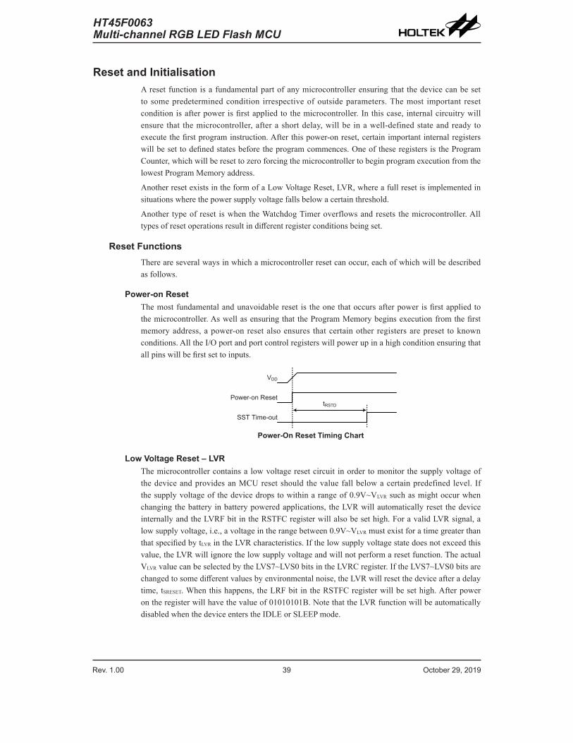
Rev. 1.00 38 October 29, 2019 Rev. 1.00 39 October 29, 2019
HT45F0063Multi-channel RGB LED Flash MCU
HT45F0063Multi-channel RGB LED Flash MCU
Reset and InitialisationA reset function is a fundamental part of any microcontroller ensuring that the device can be set to some predetermined condition irrespective of outside parameters. The most important reset condition is after power is first applied to the microcontroller. In this case, internal circuitry will ensure that the microcontroller, after a short delay, will be in a well-defined state and ready to execute the first program instruction. After this power-on reset, certain important internal registers will be set to defined states before the program commences. One of these registers is the Program Counter, which will be reset to zero forcing the microcontroller to begin program execution from the lowest Program Memory address.
Another reset exists in the form of a Low Voltage Reset, LVR, where a full reset is implemented in situations where the power supply voltage falls below a certain threshold.
Another type of reset is when the Watchdog Timer overflows and resets the microcontroller. All types of reset operations result in different register conditions being set.
Reset FunctionsThere are several ways in which a microcontroller reset can occur, each of which will be described as follows.
Power-on ResetThe most fundamental and unavoidable reset is the one that occurs after power is first applied to the microcontroller. As well as ensuring that the Program Memory begins execution from the first memory address, a power-on reset also ensures that certain other registers are preset to known conditions. All the I/O port and port control registers will power up in a high condition ensuring that all pins will be first set to inputs.
VDD
Power-on Reset
SST Time-out
tRSTD
Power-On Reset Timing Chart
Low Voltage Reset – LVRThe microcontroller contains a low voltage reset circuit in order to monitor the supply voltage of the device and provides an MCU reset should the value fall below a certain predefined level. If the supply voltage of the device drops to within a range of 0.9V~VLVR such as might occur when changing the battery in battery powered applications, the LVR will automatically reset the device internally and the LVRF bit in the RSTFC register will also be set high. For a valid LVR signal, a low supply voltage, i.e., a voltage in the range between 0.9V~VLVR must exist for a time greater than that specified by tLVR in the LVR characteristics. If the low supply voltage state does not exceed this value, the LVR will ignore the low supply voltage and will not perform a reset function. The actual VLVR value can be selected by the LVS7~LVS0 bits in the LVRC register. If the LVS7~LVS0 bits are changed to some different values by environmental noise, the LVR will reset the device after a delay time, tSRESET. When this happens, the LRF bit in the RSTFC register will be set high. After power on the register will have the value of 01010101B. Note that the LVR function will be automatically disabled when the device enters the IDLE or SLEEP mode.
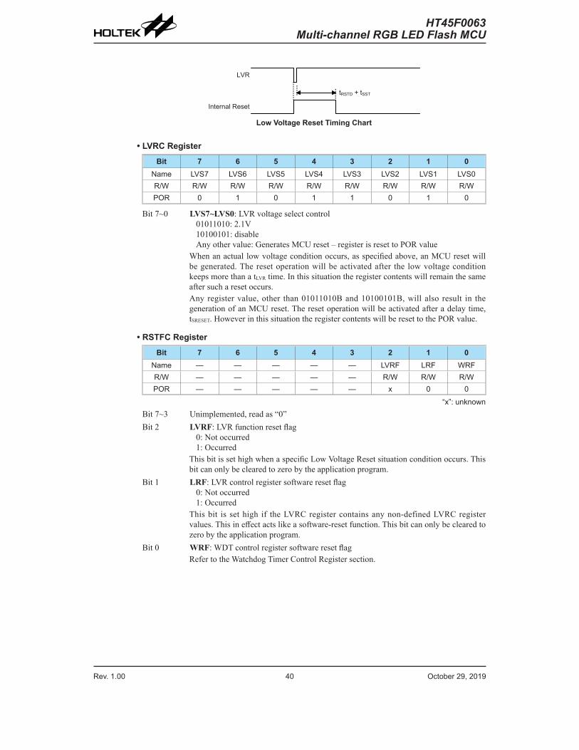
Rev. 1.00 40 October 29, 2019 Rev. 1.00 41 October 29, 2019
HT45F0063Multi-channel RGB LED Flash MCU
HT45F0063Multi-channel RGB LED Flash MCU
LVR
Internal Reset
tRSTD + tSST
Low Voltage Reset Timing Chart
• LVRC RegisterBit 7 6 5 4 3 2 1 0
Name LVS7 LVS6 LVS5 LVS4 LVS3 LVS2 LVS1 LVS0R/W R/W R/W R/W R/W R/W R/W R/W R/WPOR 0 1 0 1 1 0 1 0
Bit 7~0 LVS7~LVS0: LVR voltage select control01011010: 2.1V10100101: disableAny other value: Generates MCU reset – register is reset to POR value
When an actual low voltage condition occurs, as specified above, an MCU reset will be generated. The reset operation will be activated after the low voltage condition keeps more than a tLVR time. In this situation the register contents will remain the same after such a reset occurs.Any register value, other than 01011010B and 10100101B, will also result in the generation of an MCU reset. The reset operation will be activated after a delay time, tSRESET. However in this situation the register contents will be reset to the POR value.
• RSTFC RegisterBit 7 6 5 4 3 2 1 0
Name — — — — — LVRF LRF WRFR/W — — — — — R/W R/W R/WPOR — — — — — x 0 0
“x”: unknownBit 7~3 Unimplemented, read as “0”Bit 2 LVRF: LVR function reset flag
0: Not occurred1: Occurred
This bit is set high when a specific Low Voltage Reset situation condition occurs. This bit can only be cleared to zero by the application program.
Bit 1 LRF: LVR control register software reset flag0: Not occurred1: Occurred
This bit is set high if the LVRC register contains any non-defined LVRC register values. This in effect acts like a software-reset function. This bit can only be cleared to zero by the application program.
Bit 0 WRF: WDT control register software reset flagRefer to the Watchdog Timer Control Register section.

Rev. 1.00 40 October 29, 2019 Rev. 1.00 41 October 29, 2019
HT45F0063Multi-channel RGB LED Flash MCU
HT45F0063Multi-channel RGB LED Flash MCU
Watchdog Time-out Reset during Normal OperationThe Watchdog time-out Reset during normal operations in the FAST or SLOW mode is the same as a Power On reset except that the Watchdog time-out flag TO will be set to “1”.
WDT Time-out
Internal Reset
tRSTD
WDT Time-out Reset during Normal Operation Timing Chart
Watchdog Time-out Reset during SLEEP or IDLE ModeThe Watchdog time-out Reset during SLEEP or IDLE Mode is a little different from other kinds of reset. Most of the conditions remain unchanged except that the Program Counter and the Stack Pointer will be cleared to “0” and the TO flag will be set to “1”. Refer to the System Start Up Tim Characteristics for tSST details.
WDT Time-out
Internal Reset
tSST
WDT Time-out Reset during SLEEP or IDLE Mode Timing Chart
Reset Initial Conditions The different types of reset described affect the reset flags in different ways. These flags, known as PDF and TO are located in the status register and are controlled by various microcontroller operations, such as the SLEEP or IDLE Mode function or Watchdog Timer. The reset flags are shown in the table:
TO PDF Reset Conditions0 0 Power-on resetu u LVR reset during FAST or SLOW Mode operation1 u WDT time-out reset during FAST or SLOW Mode operation1 1 WDT time-out reset during IDLE or SLEEP Mode operation
Note: “u” stands for unchangedThe following table indicates the way in which the various components of the microcontroller are affected after a power-on reset occurs.
Item Condition after ResetProgram Counter Reset to zeroInterrupts All interrupts will be disabledWDT, Time Base Clear after reset, WDT begins countingTimer Module Timer Module will be turned offInput/Output Ports I/O ports will be set as inputsStack Pointer Stack Pointer will point to the top of the stack
The different kinds of resets all affect the internal registers of the microcontroller in different ways. To ensure reliable continuation of normal program execution after a reset occurs, it is important to know what condition the microcontroller is in after a particular reset occurs. The following table describes how each type of reset affects each of the microcontroller internal registers. Note that where more than one package type exists the table will reflect the situation for the larger package type.

Rev. 1.00 42 October 29, 2019 Rev. 1.00 43 October 29, 2019
HT45F0063Multi-channel RGB LED Flash MCU
HT45F0063Multi-channel RGB LED Flash MCU
Register Power On Reset WDT Time-out(Normal Operation)
WDT Time-out(IDLE/SLEEP)
IAR0 x x x x x x x x x x x x x x x x x u u u u u u uMP0 x x x x x x x x x x x x x x x x x u u u u u u uIAR1 x x x x x x x x x x x x x x x x x u u u u u u uMP1 x x x x x x x x x x x x x x x x x u u u u u u uBP - - - - - - 0 0 - - - - - - 0 0 - - - - - - u uACC x x x x x x x x u u u u u u u u u u u u u u u uPCL 0 0 0 0 0 0 0 0 0 0 0 0 0 0 0 0 0 0 0 0 0 0 0 0TBLP x x x x x x x x u u u u u u u u u u u u u u u uTBLH x x x x x x x x u u u u u u u u u u u u u u u uTBHP - - - - x x x x - - - - u u u u - - - - u u u uSTATUS - - 0 0 x x x x - - 1 u u u u u - - 1 1 u u u uSCC 0 0 0 - - - 0 0 0 0 0 - - - 0 0 u u u - - - u uHIRCC - - - - - - 0 1 - - - - - - 0 1 - - - - - - u uWDTC 0 1 0 1 0 0 11 0 1 0 1 0 0 11 u u u u u u u uRSTFC - - - - - x 0 0 - - - - - u u u - - - - - u u uINTC0 - 0 0 0 0 0 0 0 - 0 0 0 0 0 0 0 - u u u u u u uINTC1 - - - 0 - - - 0 - - - 0 - - - 0 - - - u - - - uMFI - - 0 0 - - 0 0 - - 0 0 - - 0 0 - - u u - - u uPA 1 1 1 1 1 1 1 1 1 1 1 1 1 1 1 1 u u u u u u u uPAC 1 1 1 1 1 1 1 1 1 1 1 1 1 1 1 1 u u u u u u u uPAPU 0 0 0 0 0 0 0 0 0 0 0 0 0 0 0 0 u u u u u u u uPAWU 0 0 0 0 0 0 0 0 0 0 0 0 0 0 0 0 u u u u u u u uPB 1 1 1 1 1 1 1 1 1 1 1 1 1 1 1 1 u u u u u u u uPBC 1 1 1 1 1 1 1 1 1 1 1 1 1 1 1 1 u u u u u u u uPBPU 0 0 0 0 0 0 0 0 0 0 0 0 0 0 0 0 u u u u u u u uPSCR - - - - - - 0 0 - - - - - - 0 0 - - - - - - u uTBC 0 - - - - 0 0 0 0 - - - - 0 0 0 u - - - - u u uPAS0 0 0 - - 0 0 0 0 0 0 - - 0 0 0 0 u u - - u u u uPAS1 0 0 0 0 0 0 0 0 0 0 0 0 0 0 0 0 u u u u u u u uPBS0 0 0 0 0 0 0 0 0 0 0 0 0 0 0 0 0 u u u u u u u uPBS1 0 0 0 0 0 0 0 0 0 0 0 0 0 0 0 0 u u u u u u u uPCS0 0 0 0 0 0 0 0 0 0 0 0 0 0 0 0 0 u u u u u u u uIFS - - - - - 0 0 0 - - - - - 0 0 0 - - - - - u u uCTMC0 0 0 0 0 0 0 0 0 0 0 0 0 0 0 0 0 u u u u u u u uCTMC1 0 0 0 0 0 0 0 0 0 0 0 0 0 0 0 0 u u u u u u u uCTMDL 0 0 0 0 0 0 0 0 0 0 0 0 0 0 0 0 u u u u u u u uCTMDH - - - - - - 0 0 - - - - - - 0 0 - - - - - - u uCTMAL 0 0 0 0 0 0 0 0 0 0 0 0 0 0 0 0 u u u u u u u uCTMAH - - - - - - 0 0 - - - - - - 0 0 - - - - - - u uCCS 0 0 1 0 1 0 1 0 0 0 1 0 1 0 1 0 u u u u u u u uIICC0 - - - - 0 0 0 - - - - - 0 0 0 - - - - - u u u -IICC1 1 0 0 0 0 0 0 1 1 0 0 0 0 0 0 1 u u u u u u u uIICD x x x x x x x x x x x x x x x x u u u u u u u uIICA 0 0 0 0 0 0 0 0 0 0 0 0 0 0 0 0 u u u u u u u uIICTOC 0 0 0 0 0 0 0 0 0 0 0 0 0 0 0 0 u u u u u u u uCCOPU0 0 0 0 0 0 0 0 0 0 0 0 0 0 0 0 0 u u u u u u u uCCOPU1 - 0 0 0 0 0 0 0 - 0 0 0 0 0 0 0 - u u u u u u u

Rev. 1.00 42 October 29, 2019 Rev. 1.00 43 October 29, 2019
HT45F0063Multi-channel RGB LED Flash MCU
HT45F0063Multi-channel RGB LED Flash MCU
Register Power On Reset WDT Time-out(Normal Operation)
WDT Time-out(IDLE/SLEEP)
PC - - - - 1 1 1 1 - - - - 1 1 1 1 - - - - u u u uPCC - - - - 1 1 1 1 - - - - 1 1 1 1 - - - - u u u uPCPU - - - - 0 0 0 0 - - - - 0 0 0 0 - - - - u u u uLVRC 0 1 0 1 1 0 1 0 0 1 0 1 1 0 1 0 u u u u u u u uBC 1 1 1 1 1 1 1 1 1 1 1 1 1 1 1 1 u u u u u u u uCASCON - 1 0 0 0 0 0 0 - 1 0 0 0 0 0 0 - u u u u u u uCASPRE - - - - - 0 0 0 - - - - - 0 0 0 - - - - - u u uCASTH - - - 0 0 1 1 1 - - - 0 0 1 1 1 - - - u u u u uD0CNT - - - 0 0 1 0 0 - - - 0 0 1 0 0 - - - u u u u uD1CNT - - - 0 1 0 1 0 - - - 0 1 0 1 0 - - - u u u u uPCNT 0 0 0 1 1 0 0 0 0 0 0 1 1 0 0 0 u u u u u u u uRCNT 1 0 0 0 0 0 0 0 1 0 0 0 0 0 0 0 u u u u u u u uCASDNB - - - - 0 0 1 1 - - - - 0 0 1 1 - - - - u u u uCASD0 0 0 0 0 0 0 0 0 0 0 0 0 0 0 0 0 u u u u u u u uCASD1 0 0 0 0 0 0 0 0 0 0 0 0 0 0 0 0 u u u u u u u uCASD2 0 0 0 0 0 0 0 0 0 0 0 0 0 0 0 0 u u u u u u u uCASD3 0 0 0 0 0 0 0 0 0 0 0 0 0 0 0 0 u u u u u u u uCASD4 0 0 0 0 0 0 0 0 0 0 0 0 0 0 0 0 u u u u u u u uCASD5 0 0 0 0 0 0 0 0 0 0 0 0 0 0 0 0 u u u u u u u uCASD6 0 0 0 0 0 0 0 0 0 0 0 0 0 0 0 0 u u u u u u u uCASD7 0 0 0 0 0 0 0 0 0 0 0 0 0 0 0 0 u u u u u u u uCASD8 0 0 0 0 0 0 0 0 0 0 0 0 0 0 0 0 u u u u u u u uCASD9 0 0 0 0 0 0 0 0 0 0 0 0 0 0 0 0 u u u u u u u uCASD10 0 0 0 0 0 0 0 0 0 0 0 0 0 0 0 0 u u u u u u u uCASD11 0 0 0 0 0 0 0 0 0 0 0 0 0 0 0 0 u u u u u u u uCASD12 0 0 0 0 0 0 0 0 0 0 0 0 0 0 0 0 u u u u u u u uCASD13 0 0 0 0 0 0 0 0 0 0 0 0 0 0 0 0 u u u u u u u uCASD14 0 0 0 0 0 0 0 0 0 0 0 0 0 0 0 0 u u u u u u u uCASD15 0 0 0 0 0 0 0 0 0 0 0 0 0 0 0 0 u u u u u u u uCASD16 0 0 0 0 0 0 0 0 0 0 0 0 0 0 0 0 u u u u u u u uCASD17 0 0 0 0 0 0 0 0 0 0 0 0 0 0 0 0 u u u u u u u uCASD18 0 0 0 0 0 0 0 0 0 0 0 0 0 0 0 0 u u u u u u u uCASD19 0 0 0 0 0 0 0 0 0 0 0 0 0 0 0 0 u u u u u u u uCASD20 0 0 0 0 0 0 0 0 0 0 0 0 0 0 0 0 u u u u u u u uCASD21 0 0 0 0 0 0 0 0 0 0 0 0 0 0 0 0 u u u u u u u uCASD22 0 0 0 0 0 0 0 0 0 0 0 0 0 0 0 0 u u u u u u u uCASD23 0 0 0 0 0 0 0 0 0 0 0 0 0 0 0 0 u u u u u u u uCASD24 0 0 0 0 0 0 0 0 0 0 0 0 0 0 0 0 u u u u u u u uCASD25 0 0 0 0 0 0 0 0 0 0 0 0 0 0 0 0 u u u u u u u uCASD26 0 0 0 0 0 0 0 0 0 0 0 0 0 0 0 0 u u u u u u u uCASD27 0 0 0 0 0 0 0 0 0 0 0 0 0 0 0 0 u u u u u u u uCASD28 0 0 0 0 0 0 0 0 0 0 0 0 0 0 0 0 u u u u u u u uCASD29 0 0 0 0 0 0 0 0 0 0 0 0 0 0 0 0 u u u u u u u uCASD30 0 0 0 0 0 0 0 0 0 0 0 0 0 0 0 0 u u u u u u u uCASD31 0 0 0 0 0 0 0 0 0 0 0 0 0 0 0 0 u u u u u u u uCASD32 0 0 0 0 0 0 0 0 0 0 0 0 0 0 0 0 u u u u u u u uCASD33 0 0 0 0 0 0 0 0 0 0 0 0 0 0 0 0 u u u u u u u u

Rev. 1.00 44 October 29, 2019 Rev. 1.00 45 October 29, 2019
HT45F0063Multi-channel RGB LED Flash MCU
HT45F0063Multi-channel RGB LED Flash MCU
Register Power On Reset WDT Time-out(Normal Operation)
WDT Time-out(IDLE/SLEEP)
CASD34 0 0 0 0 0 0 0 0 0 0 0 0 0 0 0 0 u u u u u u u uCASD35 0 0 0 0 0 0 0 0 0 0 0 0 0 0 0 0 u u u u u u u uCASD36 0 0 0 0 0 0 0 0 0 0 0 0 0 0 0 0 u u u u u u u uCASD37 0 0 0 0 0 0 0 0 0 0 0 0 0 0 0 0 u u u u u u u uCASD38 0 0 0 0 0 0 0 0 0 0 0 0 0 0 0 0 u u u u u u u uCASD39 0 0 0 0 0 0 0 0 0 0 0 0 0 0 0 0 u u u u u u u uCASD40 0 0 0 0 0 0 0 0 0 0 0 0 0 0 0 0 u u u u u u u uCASD41 0 0 0 0 0 0 0 0 0 0 0 0 0 0 0 0 u u u u u u u uCASD42 0 0 0 0 0 0 0 0 0 0 0 0 0 0 0 0 u u u u u u u uCASD43 0 0 0 0 0 0 0 0 0 0 0 0 0 0 0 0 u u u u u u u uCASD44 0 0 0 0 0 0 0 0 0 0 0 0 0 0 0 0 u u u u u u u uCASD45 0 0 0 0 0 0 0 0 0 0 0 0 0 0 0 0 u u u u u u u uCASD46 0 0 0 0 0 0 0 0 0 0 0 0 0 0 0 0 u u u u u u u uCASD47 0 0 0 0 0 0 0 0 0 0 0 0 0 0 0 0 u u u u u u u uINTCON0 0 0 0 0 0 0 0 0 0 0 0 0 0 0 0 0 u u u u u u u uINTCON1 - - - 0 - - - 0 - - - 0 - - - 0 - - - u - - - uCOM_PWM 0 - 0 0 0 0 0 0 0 - 0 0 0 0 0 0 u - u u u u u uPWM0DATA 0 0 0 0 0 0 0 0 0 0 0 0 0 0 0 0 u u u u u u u uPWM1DATA 0 0 0 0 0 0 0 0 0 0 0 0 0 0 0 0 u u u u u u u uPWM2DATA 0 0 0 0 0 0 0 0 0 0 0 0 0 0 0 0 u u u u u u u uPWM3DATA 0 0 0 0 0 0 0 0 0 0 0 0 0 0 0 0 u u u u u u u uPWM4DATA 0 0 0 0 0 0 0 0 0 0 0 0 0 0 0 0 u u u u u u u uPWM5DATA 0 0 0 0 0 0 0 0 0 0 0 0 0 0 0 0 u u u u u u u uPWM6DATA 0 0 0 0 0 0 0 0 0 0 0 0 0 0 0 0 u u u u u u u uPWM7DATA 0 0 0 0 0 0 0 0 0 0 0 0 0 0 0 0 u u u u u u u uPWM8DATA 0 0 0 0 0 0 0 0 0 0 0 0 0 0 0 0 u u u u u u u uPWM9DATA 0 0 0 0 0 0 0 0 0 0 0 0 0 0 0 0 u u u u u u u uPWM10DATA 0 0 0 0 0 0 0 0 0 0 0 0 0 0 0 0 u u u u u u u uPWM11DATA 0 0 0 0 0 0 0 0 0 0 0 0 0 0 0 0 u u u u u u u uPWM12DATA 0 0 0 0 0 0 0 0 0 0 0 0 0 0 0 0 u u u u u u u uPWM13DATA 0 0 0 0 0 0 0 0 0 0 0 0 0 0 0 0 u u u u u u u uPWM14DATA 0 0 0 0 0 0 0 0 0 0 0 0 0 0 0 0 u u u u u u u u
Note: “u” stands for unchanged“x” stands for unknown“-” stands for unimplemented

Rev. 1.00 44 October 29, 2019 Rev. 1.00 45 October 29, 2019
HT45F0063Multi-channel RGB LED Flash MCU
HT45F0063Multi-channel RGB LED Flash MCU
Input/Output PortsHoltek microcontrollers offer considerable flexibility on their I/O ports. With the input or output designation of every pin fully under user program control, pull-high selections for all ports and wake-up selections on certain pins, the user is provided with an I/O structure to meet the needs of a wide range of application possibilities.
The device provides bidirectional input/output lines labeled with port names PA~PC. These I/O ports are mapped to the RAM Data Memory with specific addresses as shown in the Special Purpose Data Memory table. All of these I/O ports can be used for input and output operations. For input operation, these ports are non-latching, which means the inputs must be ready at the T2 rising edge of instruction “MOV A, [m]”, where m denotes the port address. For output operation, all the data is latched and remains unchanged until the output latch is rewritten.
Register Name
Bit7 6 5 4 3 2 1 0
PA PA7 PA6 PA5 PA4 PA3 PA2 PA1 PA0PAC PAC7 PAC6 PAC5 PAC4 PAC3 PAC2 PAC1 PAC0PAPU PAPU7 PAPU6 PAPU5 PAPU4 PAPU3 PAPU2 PAPU1 PAPU0PAWU PAWU7 PAWU6 PAWU5 PAWU4 PAWU3 PAWU2 PAWU1 PAWU0PB PB7 PB6 PB5 PB4 PB3 PB2 PB1 PB0PBC PBC7 PBC6 PBC5 PBC4 PBC3 PBC2 PBC1 PBC0PBPU PBPU7 PBPU6 PBPU5 PBPU4 PBPU3 PBPU2 PBPU1 PBPU0PC — — — — PC3 PC2 PC1 PC0PCC — — — — PCC3 PCC2 PCC1 PCC0PCPU — — — — PCPU3 PCPU2 PCPU1 PCPU0
“—”: Unimplemented, read as “0”I/O Logic Function Register List
Pull-high ResistorsMany product applications require pull-high resistors for their switch inputs usually requiring the use of an external resistor. To eliminate the need for these external resistors, all I/O pins, when configured as a digital input have the capability of being connected to an internal pull-high resistor. These pull-high resistors are selected using the relevant pull-high control registers PxPU, and are implemented using weak PMOS transistors.
Note that the pull-high resistor can be controlled by the relevant pull-high control registers only when the pin-shared functional pin is selected as a digital input or NMOS output. Otherwise, the pull-high resistors cannot be enabled.
• PxPU RegisterBit 7 6 5 4 3 2 1 0
Name PxPU7 PxPU6 PxPU5 PxPU4 PxPU3 PxPU2 PxPU1 PxPU0R/W R/W R/W R/W R/W R/W R/W R/W R/WPOR 0 0 0 0 0 0 0 0
PxPUn: I/O Port x Pin pull-high function control0: Disable1: Enable
The PxPUn bit is used to control the pin pull-high function. Here the “x” can be A, B and C. However, the actual available bits for each I/O Port may be different.

Rev. 1.00 46 October 29, 2019 Rev. 1.00 47 October 29, 2019
HT45F0063Multi-channel RGB LED Flash MCU
HT45F0063Multi-channel RGB LED Flash MCU
Port A Wake-upThe HALT instruction forces the microcontroller into the SLEEP or IDLE Mode which preserves power, a feature that is important for battery and other low-power applications. Various methods exist to wake-up the microcontroller, one of which is to change the logic condition on one of the Port A pins from high to low. This function is especially suitable for applications that can be woken up via external switches. Each pin on Port A can be selected individually to have this wake-up feature using the PAWU register.
Note that the wake-up function can be controlled by the wake-up control registers only when the pin-shared functional pin is selected as general purpose input/output and the MCU enters the IDLE or SLEEP mode.
• PAWU RegisterBit 7 6 5 4 3 2 1 0
Name PAWU7 PAWU6 PAWU5 PAWU4 PAWU3 PAWU2 PAWU1 PAWU0R/W R/W R/W R/W R/W R/W R/W R/W R/WPOR 0 0 0 0 0 0 0 0
Bit 7~0 PAWU7~PAWU0: PA7~PA0 wake-up function control0: Disable1: Enable
I/O Port Control RegistersEach I/O port has its own control register known as PAC~PCC, to control the input/output configuration. With this control register, each CMOS output or input can be reconfigured dynamically under software control. Each pin of the I/O ports is directly mapped to a bit in its associated port control register. For the I/O pin to function as an input, the corresponding bit of the control register must be written as a “1”. This will then allow the logic state of the input pin to be directly read by instructions. When the corresponding bit of the control register is written as a “0”, the I/O pin will be set as a CMOS output. If the pin is currently set as an output, instructions can still be used to read the output register. However, it should be noted that the program will in fact only read the status of the output data latch and not the actual logic status of the output pin.
• PxC RegisterBit 7 6 5 4 3 2 1 0
Name PxC7 PxC6 PxC5 PxC4 PxC3 PxC2 PxC1 PxC0R/W R/W R/W R/W R/W R/W R/W R/W R/WPOR 1 1 1 1 1 1 1 1
PxCn: I/O Port x Pin type selection0: Output1: Input
The PxCn bit is used to control the pin type selection. Here the “x” can be A, B and C. However, the actual available bits for each I/O Port may be different.
Pin-shared FunctionsThe flexibility of the microcontroller range is greatly enhanced by the use of pins that have more than one function. Limited numbers of pins can force serious design constraints on designers but by supplying pins with multi-functions, many of these difficulties can be overcome. For these pins, the desired function of the multi-function I/O pins is selected by a series of registers via the application program control.

Rev. 1.00 46 October 29, 2019 Rev. 1.00 47 October 29, 2019
HT45F0063Multi-channel RGB LED Flash MCU
HT45F0063Multi-channel RGB LED Flash MCU
Pin-shared Function Selection RegistersThe limited number of supplied pins in a package can impose restrictions on the amount of functions a certain device can contain. However by allowing the same pins to share several different functions and providing a means of function selection, a wide range of different functions can be incorporated into even relatively small package sizes. The device includes Port “x” Output Function Selection register “n”, labeled as PxSn, and Input Function Selection register, labeled as IFS, which can select the desired functions of the multi-function pin-shared pins.
When the pin-shared input function is selected to be used, the corresponding input and output functions selection should be properly managed. For example, if the cascading transceiver interface is used, the corresponding pin-shared function should be configured as the cascading transceiver interface function by configuring the PxSn register and the cascading transceiver interface signal input pin should be properly selected using the IFS register.
The most important point to note is to make sure that the desired pin-shared function is properly selected and also deselected. For most pin-shared functions, to select the desired pin-shared function, the pin-shared function should first be correctly selected using the corresponding pin-shared control register. After that the corresponding peripheral functional setting should be configured and then the peripheral function can be enabled. However, a special point must be noted for some digital input pins, such as INT etc, which share the same pin-shared control configuration with their corresponding general purpose I/O functions when setting the relevant pin-shared control bit fields. To select these pin functions, in addition to the necessary pin-shared control and peripheral functional setup aforementioned, they must also be set as an input by setting the corresponding bit in the I/O port control register. To correctly deselect the pin-shared function, the peripheral function should first be disabled and then the corresponding pin-shared function control register can be modified to select other pin-shared functions.
Register Name
Bit7 6 5 4 3 2 1 0
PAS0 PAS07 PAS06 — — PAS03 PAS02 PAS01 PAS00PAS1 PAS17 PAS16 PAS15 PAS14 PAS13 PAS12 PAS11 PAS10PBS0 PBS07 PBS06 PBS05 PBS04 PBS03 PBS02 PBS01 PBS00PBS1 PBS17 PBS16 PBS15 PBS14 PBS13 PBS12 PBS11 PBS10PCS0 PCS07 PCS06 PCS05 PCS04 PCS03 PCS02 PCS01 PCS00IFS — — — — — IFS2 IFS1 IFS0
Pin-shared Function Selection Register List
• PAS0 RegisterBit 7 6 5 4 3 2 1 0
Name PAS07 PAS06 — — PAS03 PAS02 PAS01 PAS00R/W R/W R/W — — R/W R/W R/W R/WPOR 0 0 — — 0 0 0 0
Bit 7~6 PAS07~PAS06: PA3 Pin-shared function selection00: PA301: PA310: PA311: CCO1
Bit 5~4 Unimplemented, read as “0”

Rev. 1.00 48 October 29, 2019 Rev. 1.00 49 October 29, 2019
HT45F0063Multi-channel RGB LED Flash MCU
HT45F0063Multi-channel RGB LED Flash MCU
Bit 3~2 PAS03~PAS02: PA1 Pin-shared function selection00: PA101: PA110: PA111: CCO0
Bit 1~0 PAS01~PAS00: PA0 Pin-shared function selection00: PA001: PA010: PA011: AD
• PAS1 RegisterBit 7 6 5 4 3 2 1 0
Name PAS17 PAS16 PAS15 PAS14 PAS13 PAS12 PAS11 PAS10R/W R/W R/W R/W R/W R/W R/W R/W R/WPOR 0 0 0 0 0 0 0 0
Bit 7~6 PAS17~PAS16: PA7 Pin-shared function selection00: PA701: PA710: PA711: CCO5
Bit 5~4 PAS15~PAS14: PA6 Pin-shared function selection00: PA601: PA610: PA611: CCO4
Bit 3~2 PAS13~PAS12: PA5 Pin-shared function selection00: PA501: PA510: PA511: CCO3
Bit 1~0 PAS11~PAS10: PA4 Pin-shared function selection00: PA401: PA410: PA411: CCO2
• PBS0 RegisterBit 7 6 5 4 3 2 1 0
Name PBS07 PBS06 PBS05 PBS04 PBS03 PBS02 PBS01 PBS00R/W R/W R/W R/W R/W R/W R/W R/W R/WPOR 0 0 0 0 0 0 0 0
Bit 7~6 PBS07~PBS06: PB3 Pin-shared function selection00: PB301: PB310: PB311: CCO9
Bit 5~4 PBS05~PBS04: PB2 Pin-shared function selection00: PB201: PB210: PB211: CCO8

Rev. 1.00 48 October 29, 2019 Rev. 1.00 49 October 29, 2019
HT45F0063Multi-channel RGB LED Flash MCU
HT45F0063Multi-channel RGB LED Flash MCU
Bit 3~2 PBS03~PBS02: PB1 Pin-shared function selection00: PB101: PB110: SDA11: CCO7
Bit 1~0 PBS01~PBS00: PB0 Pin-shared function selection00: PB001: PB010: SCL11: CCO6
• PBS1 RegisterBit 7 6 5 4 3 2 1 0
Name PBS17 PBS16 PBS15 PBS14 PBS13 PBS12 PBS11 PBS10R/W R/W R/W R/W R/W R/W R/W R/W R/WPOR 0 0 0 0 0 0 0 0
Bit 7~6 PBS17~PBS16: PB7 Pin-shared function selection00: PB701: PB710: COM111: CCO13
Bit 5~4 PBS15~PBS14: PB6 Pin-shared function selection00: PB601: PB610: COM011: CCO12
Bit 3~2 PBS13~PBS12: PB5 Pin-shared function selection00: PB501: PB510: CASDI11: CCO11
Bit 1~0 PBS11~PBS10: PB4 Pin-shared function selection00: PB401: PB410: CASDO11: CCO10
• PCS0 RegisterBit 7 6 5 4 3 2 1 0
Name PCS07 PCS06 PCS05 PCS04 PCS03 PCS02 PCS01 PCS00R/W R/W R/W R/W R/W R/W R/W R/W R/WPOR 0 0 0 0 0 0 0 0
Bit 7~6 PCS07~PCS06: PC3 Pin-shared function selection00: PC301: PC310: SDA11: CASDI
Bit 5~4 PCS05~PCS04: PC2 Pin-shared function selection00: PC201: PC210: SCL11: CASDO

Rev. 1.00 50 October 29, 2019 Rev. 1.00 51 October 29, 2019
HT45F0063Multi-channel RGB LED Flash MCU
HT45F0063Multi-channel RGB LED Flash MCU
Bit 3~2 PCS03~PCS02: PC1 Pin-shared function selection00: PC101: PC110: PC111: COM3
Bit 1~0 PCS01~PCS00: PC0 Pin-shared function selection00: PC001: PC010: COM211: CCO14
• IFS RegisterBit 7 6 5 4 3 2 1 0
Name — — — — — IFS2 IFS1 IFS0R/W — — — — — R/W R/W R/WPOR — — — — — 0 0 0
Bit 7~3 Unimplemented, read as “0”Bit 2 IFS2: SDA input source pin selection
0: PC31: PB1
Bit 1 IFS1: SCL input source pin selection0: PC21: PB0
Bit 0 IFS0: CASDI input source pin selection0: PC31: PB5
I/O Pin StructuresThe accompanying diagram illustrates the internal structure of the I/O logic function. As the exact logical construction of the I/O pin will differ from this drawing, it is supplied as a guide only to assist with the functional understanding of the I/O logic function. The wide range of pin-shared structures does not permit all types to be shown.
MUX
VDD
Control Bit
Data Bit
Data Bus
Write Control Register
Chip Reset
Read Control Register
Read Data Register
Write Data Register
System Wake-up wake-up Select
I/O pin
Weak Pull-up
Pull-highRegister Select
Q
D
CK
Q
D
CK
Q
Q
S
S
PA only
Logic Function Input/Output Structure

Rev. 1.00 50 October 29, 2019 Rev. 1.00 51 October 29, 2019
HT45F0063Multi-channel RGB LED Flash MCU
HT45F0063Multi-channel RGB LED Flash MCU
Programming ConsiderationsWithin the user program, one of the first things to consider is port initialization. After a reset, all of the I/O data and port control registers will be set high. This means that all I/O pins will default to an input state, the level of which depends on the other connected circuitry and whether pull-high selections have been chosen. If the port control registers are then programmed to set some pins as outputs, these output pins will have an initial high output value unless the associated port data registers are first programmed. Selecting which pins are inputs and which are outputs can be achieved byte-wide by loading the correct values into the appropriate port control register or by programming individual bits in the port control register using the “SET [m].i” and “CLR [m].i” instructions. Note that when using these bit control instructions, a read-modify-write operation takes place. The microcontroller must first read in the data on the entire port, modify it to the required new bit values and then rewrite this data back to the output ports.
Port A has the additional capability of providing wake-up functions. When the device is in the SLEEP or IDLE Mode, various methods are available to wake the device up. One of these is a high to low transition of any of the Port A pins. Single or multiple pins on Port A can be set to have this function.
Timer Modules – TMOne of the most fundamental functions in any microcontroller device is the ability to control and measure time. To implement time related functions this device includes a Timer Module, abbreviated to the name TM. The TM is a multi-purpose timing unit and serves to provide operations such as Timer/Counter, Compare Match Output as well as being the functional unit for the generation of PWM signals. The TM has two individual interrupts. The addition of input and output pins for the TM ensures that users are provided with timing units with a wide and flexible range of features.
IntroductionThe device contains one Compact type TM having a reference name of CTM. The general features to the Compact TM will be described in this section and the detailed operation will be described in the Compact type TM section. The main features of the CTM are summarised in the accompanying table.
Function CTMTimer/Counter √Compare Match Output √PWM Output √PWM Alignment EdgePWM Adjustment Period & Duty Duty or Period
TM Function Summary
TM OperationThe Compact type TM offers a diverse range of functions, from simple timing operations to PWM signals generation. The key to understanding how the TM operates is to see it in terms of a free running counter whose value is then compared with the value of pre-programmed internal comparators. When the free running counter has the same value as the pre-programmed comparator, known as a compare match situation, a TM interrupt signal will be generated which can clear the counter and perhaps also change the condition of the TM output pin. The internal TM counter is driven by a user selectable clock source, which can be an internal clock.

Rev. 1.00 52 October 29, 2019 Rev. 1.00 53 October 29, 2019
HT45F0063Multi-channel RGB LED Flash MCU
HT45F0063Multi-channel RGB LED Flash MCU
TM Clock SourceThe clock source which drives the main counter in the TM can originate from various sources. The selection of the required clock source is implemented using the CTCK2~CTCK0 bits in the CTM control register. The clock source can be a ratio of the system clock fSYS or the internal high clock fH, the fSUB clock source.
TM InterruptsThe Compact type TM has two internal interrupts, one for each of the internal comparator A or comparator P, which generate a TM interrupt when a compare match condition occurs. When a TM interrupt is generated it can be used to clear the counter and also to change the state of the TM output signal.
TM Output SignalsThe TM has two output signals, CTP and CTPB. The CTPB is the inverted signal of the CTP output. When the TM is in the Compare Match Output Mode, these signals can be controlled by the TM to switch to a high or low level or to toggle when a compare match situation occurs. The PWM output waveforms are also reflected on CTP and CTPB.
Programming ConsiderationsThe TM Counter Registers and the Caputure/Compare CCRA register, being 10-bit, all have a low and high byte structure. The high byte can be directly accessed, but as the low byte can only be accessed via an internal 8-bit buffer, reading or writing to this register pair must be carried out in a specific way. The important point to note is that data transfer to and from the 8-bit buffer and its related low byte only takes place when a write or read operation to its corresponding high byte is executed.
As the CCRA register is implemented in the way shown in the following diagram and accessing these registers is carried out in a specific way described above, it is recommended to use the “MOV” instruction to access the CCRA low byte register, named CTMAL, using the following access procedures. Accessing the CCRA low byte register without following these access procedures will result in unpredictable values.
Data Bus
8-bit Buffer
CTMDHCTMDL
CTMAHCTMAL
CTM Counter Register (Read only)
CTM CCRA Register (Read/Write)
The following steps show the read and write procedures:
• Writing Data to CCRA ♦ Step 1. Write data to Low Byte CTMAL
– Note that here data is only written to the 8-bit buffer. ♦ Step 2. Write data to High Byte CTMAH
– Here data is written directly to the high byte registers and simultaneously data is latched from the 8-bit buffer to the Low Byte registers.
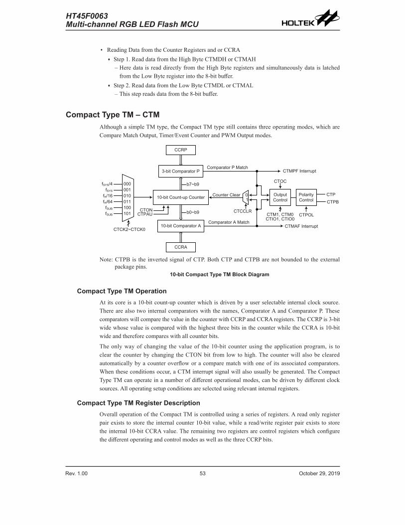
Rev. 1.00 52 October 29, 2019 Rev. 1.00 53 October 29, 2019
HT45F0063Multi-channel RGB LED Flash MCU
HT45F0063Multi-channel RGB LED Flash MCU
• Reading Data from the Counter Registers and or CCRA ♦ Step 1. Read data from the High Byte CTMDH or CTMAH
– Here data is read directly from the High Byte registers and simultaneously data is latched from the Low Byte register into the 8-bit buffer.
♦ Step 2. Read data from the Low Byte CTMDL or CTMAL – This step reads data from the 8-bit buffer.
Compact Type TM – CTMAlthough a simple TM type, the Compact TM type still contains three operating modes, which are Compare Match Output, Timer/Event Counter and PWM Output modes.
fSYS
fSYS/4
fH/64fH/16
fSUB
000001010011100101
CTCK2~CTCK0
10-bit Count-up Counter
3-bit Comparator P
CCRP
b7~b9
b0~b9
10-bit Comparator A
CTONCTPAU
Comparator A Match
Comparator P Match
Counter Clear 01
Output Control
Polarity Control
CTP
CTOC
CTM1, CTM0CTIO1, CTIO0
CTMAF Interrupt
CTMPF Interrupt
CTPOL
CCRA
CTCCLRfSUB
CTPB
Note: CTPB is the inverted signal of CTP. Both CTP and CTPB are not bounded to the external package pins.
10-bit Compact Type TM Block Diagram
Compact Type TM OperationAt its core is a 10-bit count-up counter which is driven by a user selectable internal clock source. There are also two internal comparators with the names, Comparator A and Comparator P. These comparators will compare the value in the counter with CCRP and CCRA registers. The CCRP is 3-bit wide whose value is compared with the highest three bits in the counter while the CCRA is 10-bit wide and therefore compares with all counter bits.
The only way of changing the value of the 10-bit counter using the application program, is to clear the counter by changing the CTON bit from low to high. The counter will also be cleared automatically by a counter overflow or a compare match with one of its associated comparators. When these conditions occur, a CTM interrupt signal will also usually be generated. The Compact Type TM can operate in a number of different operational modes, can be driven by different clock sources. All operating setup conditions are selected using relevant internal registers.
Compact Type TM Register DescriptionOverall operation of the Compact TM is controlled using a series of registers. A read only register pair exists to store the internal counter 10-bit value, while a read/write register pair exists to store the internal 10-bit CCRA value. The remaining two registers are control registers which configure the different operating and control modes as well as the three CCRP bits.

Rev. 1.00 54 October 29, 2019 Rev. 1.00 55 October 29, 2019
HT45F0063Multi-channel RGB LED Flash MCU
HT45F0063Multi-channel RGB LED Flash MCU
RegisterName
Bit7 6 5 4 3 2 1 0
CTMC0 CTPAU CTCK2 CTCK1 CTCK0 CTON CTRP2 CTRP1 CTRP0CTMC1 CTM1 CTM0 CTIO1 CTIO0 CTOC CTPOL CTDPX CTCCLRCTMDL D7 D6 D5 D4 D3 D2 D1 D0CTMDH — — — — — — D9 D8CTMAL D7 D6 D5 D4 D3 D2 D1 D0CTMAH — — — — — — D9 D8
10-bit Compact TM Register List• CTMC0 Register
Bit 7 6 5 4 3 2 1 0Name CTPAU CTCK2 CTCK1 CTCK0 CTON CTRP2 CTRP1 CTRP0R/W R/W R/W R/W R/W R/W R/W R/W R/WPOR 0 0 0 0 0 0 0 0
Bit 7 CTPAU: CTM counter pause control0: Run1: Pause
The counter can be paused by setting this bit high. Clearing the bit to zero restores normal counter operation. When in a pause condition the CTM will remain powered up and continue to consume power. The counter will retain its residual value when this bit changes from low to high and resume counting from this value when the bit changes to a low value again.
Bit 6~4 CTCK2~CTCK0: CTM counter clock selection000: fSYS/4001: fSYS
010: fH/16011: fH/64100: fSUB
101: fSUB
110: Undefined, cannot be used111: Undefined, cannot be used
These three bits are used to select the clock source for the CTM. The clock source fSYS is the system clock, while fH and fSUB are other internal clocks, the details of which can be found in the oscillator section.
Bit 3 CTON: CTM counter on/off control0: Off1: On
This bit controls the overall on/off function of the CTM. Setting the bit high enables the counter to run, clearing the bit disables the CTM. Clearing this bit to zero will stop the counter from counting and turn off the CTM which will reduce its power consumption. When the bit changes state from low to high the internal counter value will be reset to zero, however when the bit changes from high to low, the internal counter will retain its residual value until the bit returns high again.If the CTM is in the Compare Match Output Mode or the PWM Output Mode then the CTM output will be reset to its initial condition, as specified by the CTOC bit, when the CTON bit changes from low to high.
Bit 2~0 CTRP2~CTRP0: CTM CCRP 3-bit register, compared with the CTM Counter bit 9 ~ bit 7 Comparator P Match Period =
000: 1024 CTM clocks001: 128 CTM clocks010: 256 CTM clocks011: 384 CTM clocks100: 512 CTM clocks101: 640 CTM clocks110: 768 CTM clocks111: 896 CTM clocks

Rev. 1.00 54 October 29, 2019 Rev. 1.00 55 October 29, 2019
HT45F0063Multi-channel RGB LED Flash MCU
HT45F0063Multi-channel RGB LED Flash MCU
These three bits are used to set the value on the internal CCRP 3-bit register, which are then compared with the internal counter's highest three bits. The result of this comparison can be selected to clear the internal counter if the CTCCLR bit is set to zero. Setting the CTCCLR bit to zero ensures that a compare match with the CCRP values will reset the internal counter. As the CCRP bits are only compared with the highest three counter bits, the compare values exist in 128 clock cycle multiples. Clearing all three bits to zero is in effect allowing the counter to overflow at its maximum value.
• CTMC1 RegisterBit 7 6 5 4 3 2 1 0
Name CTM1 CTM0 CTIO1 CTIO0 CTOC CTPOL CTDPX CTCCLRR/W R/W R/W R/W R/W R/W R/W R/W R/WPOR 0 0 0 0 0 0 0 0
Bit 7~6 CTM1~CTM0: CTM operating mode selection00: Compare Match Output Mode01: Undefined10: PWM Output Mode11: Timer/Counter Mode
These bits set the required operating mode for the CTM. To ensure reliable operation the CTM should be switched off before any changes are made to the CTM1 and CTM0 bits. In the Timer/Counter Mode, the CTM output state is undefined.
Bit 5~4 CTIO1~CTIO0: CTM output function selectionCompare Match Output Mode
00: No change01: Output low10: Output high11: Toggle output
PWM Output Mode00: PWM output inactive state01: PWM output active state10: PWM output11: Undefined
Timer/Counter ModeUnused
These two bits are used to determine how the CTM output changes state when a certain condition is reached. The function that these bits select depends upon in which mode the CTM is running.In the Compare Match Output Mode, the CTIO1 and CTIO0 bits determine how the CTM output changes state when a compare match occurs from the Comparator A. The CTM output can be set to switch high, switch low or to toggle its present state when a compare match occurs from the Comparator A. When the bits are both zero, then no change will take place on the output. The initial value of the CTM output should be configured using the CTOC bit in the CTMC1 register. Note that the output level requested by the CTIO1 and CTIO0 bits must be different from the initial value setup using the CTOC bit otherwise no change will occur on the CTM output when a compare match occurs. After the CTM output changes state, it can be reset to its initial level by changing the level of the CTON bit from low to high.In the PWM Output Mode, the CTIO1 and CTIO0 bits determine how the CTM output changes state when a certain compare match condition occurs. The PWM output function is modified by changing these two bits. It is necessary to only change the values of the CTIO1 and CTIO0 bits only after the CTM has been switched off. Unpredictable PWM outputs will occur if the CTIO1 and CTIO0 bits are changed when the CTM is running.

Rev. 1.00 56 October 29, 2019 Rev. 1.00 57 October 29, 2019
HT45F0063Multi-channel RGB LED Flash MCU
HT45F0063Multi-channel RGB LED Flash MCU
Bit 3 CTOC: CTM CTP output controlCompare Match Output Mode
0: Initial low1: Initial high
PWM Output Mode0: Active low1: Active high
This is the output control bit for the CTM output. Its operation depends upon whether CTM is being used in the Compare Match Output Mode or in the PWM Output Mode. It has no effect if the CTM is in the Timer/Counter Mode. In the Compare Match Output Mode it determines the logic level of the CTM output before a compare match occurs. In the PWM Output Mode it determines if the PWM signal is active high or active low.
Bit 2 CTPOL: CTM CTP output polarity control0: Non-invert1: Invert
This bit controls the polarity of the CTP output. When the bit is set high the CTM output will be inverted and not inverted when the bit is zero. It has no effect if the TM is in the Timer/Counter Mode.
Bit 1 CTDPX: CTM PWM duty/period control0: CCRP – period; CCRA – duty1: CCRP – duty; CCRA – period
This bit determines which of the CCRA and CCRP registers are used for period and duty control of the PWM waveform.
Bit 0 CTCCLR: CTM Counter Clear condition selection0: CTM Comparator P match1: CTM Comparator A match
This bit is used to select the method which clears the counter. Remember that the Compact TM contains two comparators, Comparator A and Comparator P, either of which can be selected to clear the internal counter. With the CTCCLR bit set high, the counter will be cleared when a compare match occurs from the Comparator A. When the bit is low, the counter will be cleared when a compare match occurs from the Comparator P or with a counter overflow. A counter overflow clearing method can only be implemented if the CCRP bits are all cleared to zero. The CTCCLR bit is not used in the PWM Output Mode.
• CTMDL RegisterBit 7 6 5 4 3 2 1 0
Name D7 D6 D5 D4 D3 D2 D1 D0R/W R R R R R R R RPOR 0 0 0 0 0 0 0 0
Bit 7~0 D7~D0: CTM Counter Low Byte Register bit 7 ~ bit 0CTM 10-bit Counter bit 7 ~ bit 0
• CTMDH RegisterBit 7 6 5 4 3 2 1 0
Name — — — — — — D9 D8R/W — — — — — — R RPOR — — — — — — 0 0
Bit 7~2 Unimplemented, read as “0”Bit 1~0 D9~D8: CTM Counter High Byte Register bit 1 ~ bit 0
CTM 10-bit Counter bit 9 ~ bit 8

Rev. 1.00 56 October 29, 2019 Rev. 1.00 57 October 29, 2019
HT45F0063Multi-channel RGB LED Flash MCU
HT45F0063Multi-channel RGB LED Flash MCU
• CTMAL RegisterBit 7 6 5 4 3 2 1 0
Name D7 D6 D5 D4 D3 D2 D1 D0R/W R/W R/W R/W R/W R/W R/W R/W R/WPOR 0 0 0 0 0 0 0 0
Bit 7~0 D7~D0: CTM CCRA Low Byte Register bit 7 ~ bit 0CTM 10-bit CCRA bit 7 ~ bit 0
• CTMAH RegisterBit 7 6 5 4 3 2 1 0
Name — — — — — — D9 D8R/W — — — — — — R/W R/WPOR — — — — — — 0 0
Bit 7~2 Unimplemented, read as “0”Bit 1~0 D9~D8: CTM CCRA High Byte Register bit 1 ~ bit 0
CTM 10-bit CCRA bit 9 ~ bit 8
Compact Type TM Operating ModesThe Compact Type TM can operate in one of three operating modes, Compare Match Output Mode, PWM Output Mode or Timer/Counter Mode. The operating mode is selected using the CTM1 and CTM0 bits in the CTMC1 register.
Compare Match Output ModeTo select this mode, bits CTM1 and CTM0 in the CTMC1 register, should be set to “00” respectively. In this mode once the counter is enabled and running it can be cleared by three methods. These are a counter overflow, a compare match from Comparator A and a compare match from Comparator P. When the CTCCLR bit is low, there are two ways in which the counter can be cleared. One is when a compare match occurs from Comparator P, the other is when the CCRP bits are all zero which allows the counter to overflow. Here both CTMAF and CTMPF interrupt request flags for the Comparator A and Comparator P respectively, will both be generated.
If the CTCCLR bit in the CTMC1 register is high then the counter will be cleared when a compare match occurs from Comparator A. However, here only the CTMAF interrupt request flag will be generated even if the value of the CCRP bits is less than that of the CCRA registers. Therefore when CTCCLR is high no CTMPF interrupt request flag will be generated. If the CCRA bits are all zero, the counter will overflow when it reaches its maximum 10-bit, 3FF Hex, value, however here the CTMAF interrupt request flag will not be generated.
As the name of the mode suggests, after a comparison is made, the CTM output will change state. The CTM output condition however only changes state when a CTMAF interrupt request flag is generated after a compare match occurs from Comparator A. The CTMPF interrupt request flag, generated from a compare match occurs from Comparator P, will have no effect on the CTM output. The way in which the CTM output changes state are determined by the condition of the CTIO1 and CTIO0 bits in the CTMC1 register. The CTM output can be selected using the CTIO1 and CTIO0 bits to go high, to go low or to toggle from its present condition when a compare match occurs from Comparator A. The initial condition of the CTM output, which is configured after the CTON bit changes from low to high, is configured using the CTOC bit. Note that if the CTIO1 and CTIO0 bits are zero then no output change will take place.
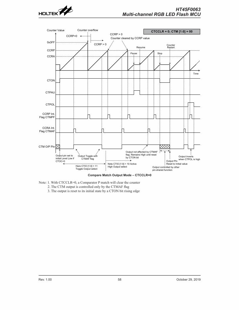
Rev. 1.00 58 October 29, 2019 Rev. 1.00 59 October 29, 2019
HT45F0063Multi-channel RGB LED Flash MCU
HT45F0063Multi-channel RGB LED Flash MCU
Counter Value
0x3FF
CCRP
CCRA
CTON
CTPAU
CTPOL
CCRP Int. Flag CTMPF
CCRA Int. Flag CTMAF
CTM O/P Pin
Time
CCRP=0
CCRP > 0
Counter overflow
CCRP > 0
Counter cleared by CCRP value
Pause
Resume
Stop
Counter Restart
CTCCLR = 0; CTM [1:0] = 00
Output pin set to initial Level Low if CTOC=0
Output Toggle with CTMAF flag
Note CTIO [1:0] = 10 Active High Output selectHere CTIO [1:0] = 11
Toggle Output select
Output not affected by CTMAF flag. Remains High until reset by CTON bit
Output PinReset to Initial value
Output controlled by other pin-shared function
Output Invertswhen CTPOL is high
Compare Match Output Mode – CTCCLR=0
Note: 1. With CTCCLR=0, a Comparator P match will clear the counter2. The CTM output is controlled only by the CTMAF flag3. The output is reset to its initial state by a CTON bit rising edge

Rev. 1.00 58 October 29, 2019 Rev. 1.00 59 October 29, 2019
HT45F0063Multi-channel RGB LED Flash MCU
HT45F0063Multi-channel RGB LED Flash MCU
Counter Value
0x3FF
CCRP
CCRA
CTON
CTPAU
CTPOL
CTM O/P Pin
Time
CCRA=0
CCRA = 0Counter overflow
CCRA > 0 Counter cleared by CCRA value
Pause
Resume
Stop Counter Restart
Output pin set to initial Level Low if CTOC=0
Output Toggle with CTMAF flag
Note CTIO [1:0] = 10 Active High Output selectHere CTIO [1:0] = 11
Toggle Output select
Output not affected by CTMAF flag. Remains High until reset by CTON bit
Output PinReset to Initial value
Output controlled by other pin-shared function
Output Invertswhen CTPOL is high
CTMPF not generated
No CTMAF flag generated on CCRA overflow
Output does not change
CTCCLR = 1; CTM [1:0] = 00
CCRA Int. Flag CTMAF
CCRP Int. Flag CTMPF
Compare Match Output Mode – CTCCLR=1
Note: 1. With CTCCLR=1, a Comparator A match will clear the counter2. The CTM output is controlled only by the CTMAF flag3. The output is reset to its initial state by a CTON bit rising edge4. The CTMPF flag is not generated when CTCCLR=1
Rev. 1.00 60 October 29, 2019 Rev. 1.00 61 October 29, 2019
HT45F0063Multi-channel RGB LED Flash MCU
HT45F0063Multi-channel RGB LED Flash MCU
Timer/Counter Mode To select this mode, bits CTM1 and CTM0 in the CTMC1 register should be set to “11” respectively. The Timer/Counter Mode operates in an identical way to the Compare Match Output Mode generating the same interrupt flags. The exception is that in the Timer/Counter Mode the CTM output is not used. Therefore the above description and Timing Diagrams for the Compare Match Output Mode can be used to understand its function. As the CTM output pin is not used in this mode, the pin can be used as a normal I/O pin or other pin-shared function.
PWM Output Mode To select this mode, bits CTM1 and CTM0 in the CTMC1 register should be set to “10” respectively. The PWM function within the CTM is useful for applications which require functions such as motor control, heating control, illumination control etc. By providing a signal of fixed frequency but of varying duty cycle on the CTM output, a square wave AC waveform can be generated with varying equivalent DC RMS values.
As both the period and duty cycle of the PWM waveform can be controlled, the choice of generated waveform is extremely flexible. In the PWM Output Mode, the CTCCLR bit has no effect on the PWM operation. Both of the CCRA and CCRP registers are used to generate the PWM waveform, one register is used to clear the internal counter and thus control the PWM waveform frequency, while the other one is used to control the duty cycle. Which register is used to control either frequency or duty cycle is determined using the CTDPX bit in the CTMC1 register. The PWM waveform frequency and duty cycle can therefore be controlled by the values in the CCRA and CCRP registers.
An interrupt flag, one for each of the CCRA and CCRP, will be generated when a compare match occurs from either Comparator A or Comparator P. The CTOC bit in the CTMC1 register is used to select the required polarity of the PWM waveform while the two CTIO1 and CTIO0 bits are used to enable the PWM output or to force the CTM output to a fixed high or low level. The CTPOL bit is used to reverse the polarity of the PWM output waveform.
• 10-bit CTM, PWM Output Mode, Edge-aligned Mode, CTDPX=0CCRP 1~7 0Period CCRP×128 1024Duty CCRA
If fSYS=8MHz, CTM clock source is fSYS/4, CCRP=2, CCRA=128,
The CTM PWM output frequency=(fSYS/4)/(2×128)=fSYS/1024=7.812kHz, duty=128/(2×128)=50%.
If the Duty value defined by the CCRA register is equal to or greater than the Period value, then the PWM output duty is 100%.
• 10-bit CTM, PWM Output Mode, Edge-aligned Mode, CTDPX=1CCRP 1~7 0Period CCRADuty CCRP×128 1024
The PWM output period is determined by the CCRA register value together with the CTM clock while the PWM duty cycle is defined by the CCRP register value.
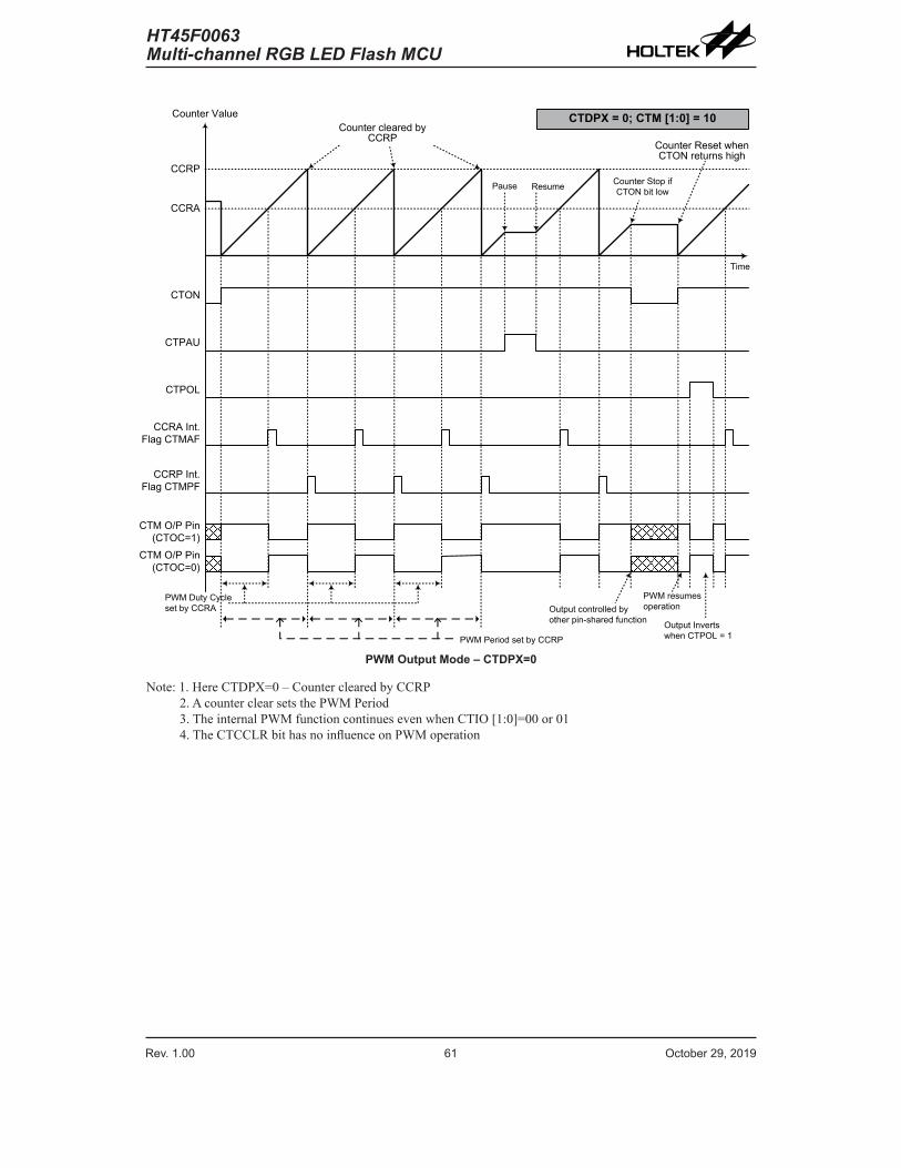
Rev. 1.00 60 October 29, 2019 Rev. 1.00 61 October 29, 2019
HT45F0063Multi-channel RGB LED Flash MCU
HT45F0063Multi-channel RGB LED Flash MCU
Counter Value
CCRP
CCRA
CTON
CTPAU
CTPOL
CTM O/P Pin (CTOC=1)
Time
Counter cleared by CCRP
Pause ResumeCounter Stop if CTON bit low
Counter Reset when CTON returns high
PWM Duty Cycle set by CCRA
PWM resumes operationOutput controlled by
other pin-shared functionOutput Invertswhen CTPOL = 1PWM Period set by CCRP
CTM O/P Pin (CTOC=0)
CCRA Int. Flag CTMAF
CCRP Int. Flag CTMPF
CTDPX = 0; CTM [1:0] = 10
PWM Output Mode – CTDPX=0
Note: 1. Here CTDPX=0 – Counter cleared by CCRP2. A counter clear sets the PWM Period3. The internal PWM function continues even when CTIO [1:0]=00 or 014. The CTCCLR bit has no influence on PWM operation

Rev. 1.00 62 October 29, 2019 Rev. 1.00 63 October 29, 2019
HT45F0063Multi-channel RGB LED Flash MCU
HT45F0063Multi-channel RGB LED Flash MCU
Counter Value
CCRP
CCRA
CTON
CTPAU
CTPOL
CCRP Int. Flag CTMPF
CCRA Int. Flag CTMAF
CTM O/P Pin (CTOC=1)
Time
Counter cleared by CCRA
Pause ResumeCounter Stop if CTON bit low
Counter Reset when CTON returns high
PWM Duty Cycle set by CCRP
PWM resumes operationOutput controlled by
other pin-shared function Output Invertswhen CTPOL = 1
PWM Period set by CCRA
CTM O/P Pin (CTOC=0)
CTDPX = 1; CTM [1:0] = 10
PWM Output Mode – CTDPX=1
Note: 1. Here CTDPX=1 – Counter cleared by CCRA2. A counter clear sets the PWM Period3. The internal PWM function continues even when CTIO [1:0]=00 or 014. The CTCCLR bit has no influence on PWM operation

Rev. 1.00 62 October 29, 2019 Rev. 1.00 63 October 29, 2019
HT45F0063Multi-channel RGB LED Flash MCU
HT45F0063Multi-channel RGB LED Flash MCU
Cascading Transceiver InterfaceThe cascade function is a feature of the LED tape light. It can be issued from a master MCU, and transfer PWM data for RGB color LED by single line cascading transceiver interface. The transfer rate is as soon as possible to make RGB LED change color smoothly. It should be noted that when the cascading transceiver is the master device, the TX function is active.
The Single Line Cascading Transceiver interface is a one-way transmission interface which contains an input CASDI pin and an output CASDO pin. Every 24 bits of data, once being received by the RX circuit, can be used to turn on a group of RGB LEDs. When the RX circuit has received full 24×N bits of data, where N ranges from 1 to 16 and is determined by application requirements and selected by the CASDNB register, the transceiver will enable the bypass path to the next device, and the next device will continue to read the following 24×N bits of data. The interception of 24×N bits of data in this sequence is called cascade function.
CASDICASDO
CASD28[7:0]
CASD27[7:0]
CASD29[7:0]
Noise Filter
1
0
8-bit Shift Register
FULL24XNEMPTY24
CASMOD
CASMOD
CASPRE
TX Circuit
D0CNT(5-bit)
PCNT(8-bit)fCAS1
fCAS1
fCAS2 = fCAS1/16
CASRES
RX Circuit
CASTH(5-bit)
PASSEN
TRGTX
fCAS2
RCNT(8-bit)
BITERR
CASRXEN
CASPRE[2:0]
fCAS1
D1CNT(5-bit)
fCAS1
PCNTEN
fCAS1
BITERR
CASMODCASEN
fCASCLKI
FULL24
CASD31[7:0]
CASD30[7:0]
CASD32[7:0]
CASD34[7:0]
CASD33[7:0]
CASD35[7:0]
CASD19[7:0]
CASD18[7:0]
CASD20[7:0]
CASD22[7:0]
CASD21[7:0]
CASD23[7:0]
CASD25[7:0]
CASD24[7:0]
CASD26[7:0]
CASD10[7:0]
CASD9[7:0]
CASD11[7:0]
CASD13[7:0]
CASD12[7:0]
CASD14[7:0]
CASD16[7:0]
CASD15[7:0]
CASD17[7:0]
CASD1[7:0]
CASD0[7:0]
CASD2[7:0]
CASD4[7:0]
CASD3[7:0]
CASD5[7:0]
CASD7[7:0]
CASD6[7:0]
CASD8[7:0]
CASD37[7:0]
CASD36[7:0]
CASD38[7:0]
CASD40[7:0]
CASD39[7:0]
CASD41[7:0]
CASD43[7:0]
CASD42[7:0]
CASD44[7:0]
CASD46[7:0]
CASD45[7:0]
CASD47[7:0]
Note: 1. The cascade clock fCASCLKI is sourced from the system clock fSYS.2. TX buffer: CASD0~CASD2;
RX buffer for direct driving: CASD0~CASD14; RX buffer for 3×COM scanning: CASD0~CASD35; RX buffer for 4×COM scanning: CASD0~CASD47.
Cascading Transceiver Interface Block Diagram

Rev. 1.00 64 October 29, 2019 Rev. 1.00 65 October 29, 2019
HT45F0063Multi-channel RGB LED Flash MCU
HT45F0063Multi-channel RGB LED Flash MCU
CASD0 CASD1 CASD2
First bit for transmission
Bit7,Bit6…………Bit0 CASD47
Bit7,Bit6…………Bit0 Bit7,Bit6…………Bit0 Bit7,Bit6…………Bit0
24×N bits (Ex. 120 bits) data= CASD0(8-bit)+CASD1(8-bit)+CASD2(8-bit)+CASD3(8-bit)+CASD4(8-bit)+CASD5(8-bit)+CASD6(8-bit)+CASD7(8-bit)+CASD8(8-bit)+CASD9(8-bit)+CASD10(8-bit)+CASD11(8-bit)CASD12(8-bit)+CASD13(8-bit)+CASD14(8-bit)
Logic 0 Data
tTX_D0H
tBIT
tTX_D0H=Logic 0 high level count
tBIT=Bit time period
tTX_D0L=Logic 0 low level count=tBIT - tTX_D0H
Hang time ≥ tRESET→ Transceiver reset
Logic 1 Data
tRESET=Reset time count
tTX_D1H
tBIT
tTX_D0LtTX_D1L
tTX_D1H=Logic 1 high level count
tTX_D1L=Logic 1 low level count=tBIT - tTX_D1H
Single Line Cascading Transceiver Interface Data Sequence
Cascading Transceiver Interface Register DescriptionOverall operation of the Cascading Transceiver Interface is controlled using a series of registers. The CASCON, INTCON0 and INTCON1 registers are used for various cascading transceiver RX and TX function controls and interrupt control. The CASPRE register is used to select cascading transceiver clock. The CASTH register is used to specify the cascading transceiver RX function input data judgment threshold value. The D0CNT and D1CNT registers are used to control the cascading transceiver TX function logic 0 and logic 1 output data. The PCNT and RCNT registers are used to control the cascading transceiver data bit time period and reset time period. The CASDNB register is used to select the data length to be received in the RX mode. The CASD0~CASD47 data registers are used to store the data received or to be transmitted.
RegisterName
Bit7 6 5 4 3 2 1 0
CASCON — PCNTEN CASRXEN D4 TRGTX PASSEN CASMOD CASENCASPRE — — — — — CASPRE2 CASPRE1 CASPRE0CASTH — — — THS4 THS3 THS2 THS1 THS0D0CNT — — — LCNT4 LCNT3 LCNT2 LCNT1 LCNT0D1CNT — — — HCNT4 HCNT3 HCNT2 HCNT1 HCNT0PCNT PS7 PS6 PS5 PS4 PS3 PS2 PS1 PS0RCNT RS7 RS6 RS5 RS4 RS3 RS2 RS1 RS0CASDNB — — — — D3 D2 D1 D0CASDn D7 D6 D5 D4 D3 D2 D1 D0INTCON0 BITERR CASRES EMPTY24 FULL24XN BERINTEN RESINTEN EPTINTEN FULINTENINTCON1 — — — FULL24 — — — INT24EN
Cascading Transceiver Interface Register List (n=0~47)

Rev. 1.00 64 October 29, 2019 Rev. 1.00 65 October 29, 2019
HT45F0063Multi-channel RGB LED Flash MCU
HT45F0063Multi-channel RGB LED Flash MCU
• CASCON RegisterBit 7 6 5 4 3 2 1 0
Name — PCNTEN CASRXEN D4 TRGTX PASSEN CASMOD CASENR/W — R/W R/W R/W R/W R/W R/W R/WPOR — 1 0 0 0 0 0 0
Bit 7 Unimplemented, read as “0”Bit 6 PCNTEN: Cascading transceiver RX/TX transfer bit time counter control
0: Disable1: Enable
This bit is used to count the RX or TX data transfer bit time period. When the PCNTEN bit is cleared to 0, the bit time counter PCNT function will be disabled in the RX mode. It means that the bit time will not be checked and then the BITERR flag will always be 0. For the TX mode the PCNT is always enabled and the PCNTEN bit has no effect on the PCNT function.When the PCNTEN bit is set to 1, the bit time counter PCNT function will be enabled. For the TX function the bit time counter is used to define the transmit bit time. For the RX function the bit time counter is used to define the maximum bit time. If the bit time counter underflows and no second rising edge appear on the CASDI line, the BITERR flag will be set to 1.
Bit 5 CASRXEN: Cascading transceiver RX function enable control0: Disable1: Enable
This bit is used to control the cascading transceiver RX function. When this bit is set to 1, the cascading transceiver RX function will be enabled. This bit will automatically be cleared to 0 when the RX shift register full flag, FULL24XN, is set high. Then it will automatically be set to 1 again when the cascading transceiver reset flag, CASRES, is set high. When this bit is set to 0, the cascading transceiver RX function will be disabled. However, the cascading transceiver reset signal can still be decoded and recognized as the RX function is disabled. Note that the PASSEN bit will automatically be cleared to 0 by hardware when the CASRXEN bit is set to 1 by hardware and vice versa.
Bit 4 D4: Reserved bit, should be fixed at “0”Bit 3 TRGTX: Cascading transceiver TX output buffer trigger control
0: No action or data is transmitted completely1: TX buffer output is triggered and data is transmitting continuously
This bit can only be written with a value of “1” when the CASEN bit is high. The TRGTX bit will be cleared to 0 by hardware when the TX shift register empty flag, EMPTY24, is set high. It will also be cleared to 0 when the CASEN bit is set low. Note that the EMPTY 24 bit will be cleared to 0 by hardware when the TRGTX bit is set high by software regardless of the transceiver operation modes. Setting the TRGTX bit in the RX mode will have no operation.
Bit 2 PASSEN: Cascading transceiver input signal bypass RX circuit enable control0: Disable – Not bypass the RX circuit1: Enable – Bypass the RX circuit
This bit controls the cascading transceiver input signal bypass function. It will automatically be set and cleared by hardware. When the CASRXEN bit is set to 1 by hardware to enable the cascading transceiver RX function, the PASSEN bit will automatically be set to 0 by hardware and the cascading transceiver input signal will be decoded by the RX circuit. When the CASRXEN bit is cleared to 0 by hardware to disable the cascading transceiver RX function, the PASSEN bit will automatically be set to 1 by hardware. At the same time the cascading transceiver input signal will bypass the RX circuit and directly be connected to the CASDO line.

Rev. 1.00 66 October 29, 2019 Rev. 1.00 67 October 29, 2019
HT45F0063Multi-channel RGB LED Flash MCU
HT45F0063Multi-channel RGB LED Flash MCU
Bit 1 CASMOD: Cascading transceiver TX or RX mode selection0: RX mode1: TX mode
This bit can only be modified when the CASEN bit is set low. The cascading transceiver operating mode should first be selected followed by setting the CASEN bit high.
Bit 0 CASEN: Cascading transceiver enable control0: Disable1: Enable
This bit is used to enable or disable the cascading transceiver function. When it is cleared to 0 to disable the cascading transceiver function, only the internal control circuit and corresponding read-only flags in the INTCON0 and INTCON1 registers together with the TRGTX bit will be reset. Other registers contents will be kept unchanged. Note that in the RX mode the contents of the CASD0~CASD47 registers will be unknown when the CASEN bit is set low. When the CASEN bit is set low, the CASDI input path will be switched off and the CASDO output will be floating.
• CASPRE RegisterBit 7 6 5 4 3 2 1 0
Name — — — — — CASPRE2 CASPRE1 CASPRE0R/W — — — — — R/W R/W R/WPOR — — — — — 0 0 0
Bit 7~3 Unimplemented, read as “0”Bit 2~0 CASPRE2~CASPRE0: Cascading transceiver clock fCAS1 division ratio selection
000: fCAS1=fCASCLKI
001: fCAS1=fCASCLKI/2010: fCAS1=fCASCLKI/4011: fCAS1=fCASCLKI/8100: fCAS1=fCASCLKI/16101: fCAS1=fCASCLKI/32110: fCAS1=fCASCLKI/64111: fCAS1=fCASCLKI/128
These bits are used to select the cascading transceiver clock fCAS1 division ratio. The fCASCLKI clock is the cascading transceiver input clock which is sourced from the system clock fSYS. The fCAS1 clock is used to drive the whole cascading transceiver circuits except the reset time counter, RCNT. The reset time counter, RCNT, is driven by the clock, fCAS2, where fCAS2=fCAS1/16.
• CASTH RegisterBit 7 6 5 4 3 2 1 0
Name — — — THS4 THS3 THS2 THS1 THS0R/W — — — R/W R/W R/W R/W R/WPOR — — — 0 0 1 1 1
Bit 7~5 Unimplemented, read as “0”Bit 4~0 THS4~THS0: Cascading transceiver RX function data judgment threshold
Logic 0 threshold: tRX_DT0HS=(THS[4:0]-2)×tCAS1
Logic 1 threshold: tRX_DT1HS=(THS[4:0]+1)×tCAS1
where tCAS1=1/fCAS1
These bits are used to specify the cascading transceiver RX function input data judgment threshold value. When the input signal high level period is equal to or greater than the tRX_DT1HS threshold, the input data will be recognized as a logic 1. However, the input data will be recognized as a logic 0 if the input signal high level period is equal to or less than the tRX_DT0HS threshold. The received data will be stored in the CASD0~CASD47 registers.
Rev. 1.00 66 October 29, 2019 Rev. 1.00 67 October 29, 2019
HT45F0063Multi-channel RGB LED Flash MCU
HT45F0063Multi-channel RGB LED Flash MCU
• D0CNT RegisterBit 7 6 5 4 3 2 1 0
Name — — — LCNT4 LCNT3 LCNT2 LCNT1 LCNT0R/W — — — R/W R/W R/W R/W R/WPOR — — — 0 0 1 0 0
Bit 7~5 Unimplemented, read as “0”Bit 4~0 LCNT4~LCNT0: Cascading transceiver TX function output data logic 0 high pulse
count value, tTX_D0H
tTX_D0H=LCNT[4:0]×tCAS1, where tCAS1=1/fCAS1
These bits are used to specify the high pulse count value of the cascading transceiver TX function logic 0 output data, which is driven by the fCAS1 clock. When the transmitted data stored in the CASDn register is logic 0, a signal with a high pulse width of tTX_D0H and a low pulse width of (tBIT-tTX_D0H) will be output on the CASDO line, where the bit time tBIT is specified by the bit time counter PCNT. The LCNT field minimum value should be properly configured according to the corresponding cascading transceiver input clock frequency, fCASCLKI, for applications.
• D1CNT RegisterBit 7 6 5 4 3 2 1 0
Name — — — HCNT4 HCNT3 HCNT2 HCNT1 HCNT0R/W — — — R/W R/W R/W R/W R/WPOR — — — 0 1 0 1 0
Bit 7~5 Unimplemented, read as “0”Bit 4~0 HCNT4~HCNT0: Cascading transceiver TX function output data logic 1 high pulse
count value, tTX_D1H
tTX_D1H=HCNT[4:0]×tCAS1, where tCAS1=1/fCAS1
These bits are used to specify the high pulse count value of the cascading transceiver TX function logic 1 output data, which is driven by the fCAS1 clock. When the transmitted data stored in the CASDn register is logic 1, a signal with a high pulse width of tTX_D1H and a low pulse width of (tBIT-tTX_D1H) will be output on the CASDO line, where the bit time tBIT is specified by the bit time counter PCNT. The HCNT field minimum value should be properly configured according to the corresponding cascading transceiver input clock frequency, fCASCLKI, for applications.
• PCNT RegisterBit 7 6 5 4 3 2 1 0
Name PS7 PS6 PS5 PS4 PS3 PS2 PS1 PS0R/W R/W R/W R/W R/W R/W R/W R/W R/WPOR 0 0 0 1 1 0 0 0
Bit 7~0 PS7~PS0: Cascading transceiver bit time counterTX mode: tBIT=PS[7:0]×tCAS1
RX mode: tBIT<(PS[7:0]-1)×tCAS1
where tCAS1=1/fCAS1
This counter is used to specify the count value of the cascading transceiver data bit time period. The bit time counter is driven by the fCAS1 clock. For the TX function the bit time counter is always enabled regardless of the PCNTEN bit status. In the TX mode the bit time is calculated as the above formula shown. When the TRGTX bit is set to 1 in the TX mode, the PCNT and D0CNT or D1CNT counters will start to count. A signal with a high pulse of tTX_D0H or tTX_D1H and a low pulse of (tBIT-tTX_D0H) or (tBIT-tTX_D1H) representing a logic data 0 or 1 respectively will be output on the CASDO line.

Rev. 1.00 68 October 29, 2019 Rev. 1.00 69 October 29, 2019
HT45F0063Multi-channel RGB LED Flash MCU
HT45F0063Multi-channel RGB LED Flash MCU
For the RX function the bit time counter is also used to check whether the error condition on the received data occurs or not other than to specify the bit time. When the PCNT function is enabled by setting the PCNTEN bit high and there is a rising edge on the CASDI line, the bit time counter PCNT will start to count down. If there is no second rising edge on the CASDI line before the PCNT counter counts down to zero for the received data bit 0 ~ bit (24×N-2), the bit error flag, BITERR, will automatically be set to 1, which means a bit transfer error occurs. For the data bit (24×N-1) reception if a falling edge appears on the CASDI line before the PCNT counter counts down to zero, the RX shift register full flags, FULL24XN and FULL24, will be set to 1. It means that the whole 24×N bits of data has been completely received. Then the PASSEN bit will automatically be set to 1 by hardware. If there is no falling edge on the CASDI line when receiving the data bit (24×N-1) before the PCNT counter counts down to zero, the bit error flag, BITERR, will also be set to 1 by hardware to indicate that a bit transfer error occurs. In this case the FULL24XN and FULL24 flags are cleared. The PASSEN bit will then be kept unchanged with a low level state.
• RCNT RegisterBit 7 6 5 4 3 2 1 0
Name RS7 RS6 RS5 RS4 RS3 RS2 RS1 RS0R/W R/W R/W R/W R/W R/W R/W R/W R/WPOR 1 0 0 0 0 0 0 0
Bit 7~0 RS7~RS0: Cascading transceiver reset time countertRESET=RS[7:0]×tCAS2, where tCAS2=1/fCAS2=16/fCAS1=16×tCAS1
This down-counter is used to specify the count value of the cascading transceiver reset time period in the RX function. The reset time counter is driven by the fCAS2 clock where the fCAS2 clock is equal to the fCAS1 clock divided by 16. When the CASMOD bit is set to 0 to select the RX mode and the CASEN bit is set to 1 to enable the cascading transceiver function, the RCNT counter will start to count. If the CASDI line signal is kept at a high or low level for a certain time period and the RCNT counts down to zero, the cascading transceiver reset flag, CASRES, will be set to 1 to indicate that a cascading transceiver reset condition occurs. When the CASRES bit is set to 1, the BITERR, FULL24XN, FULL24, PASSEN bits will be cleared to 0 and the CASRXEN bit will be set to 1.
• CASDNB RegisterBit 7 6 5 4 3 2 1 0
Name — — — — D3 D2 D1 D0R/W — — — — R/W R/W R/W R/WPOR — — — — 0 0 1 1
Bit 7~4 Unimplemented, read as “0”Bit 3~0 D3~D0: 24×N bits for cascading, RX mode only
0000: N=10001: N=20010: N=30011: N=40100: N=50101: N=60110: N=70111: N=81000: N=91001: N=101010: N=111011: N=121100: N=131101: N=141110: N=151111: N=16

Rev. 1.00 68 October 29, 2019 Rev. 1.00 69 October 29, 2019
HT45F0063Multi-channel RGB LED Flash MCU
HT45F0063Multi-channel RGB LED Flash MCU
• CASDn Register (n=0~2)Bit 7 6 5 4 3 2 1 0
Name D7 D6 D5 D4 D3 D2 D1 D0R/W R/W R/W R/W R/W R/W R/W R/W R/WPOR 0 0 0 0 0 0 0 0
Bit 7~0 D7~D0: Data byte n This register is used to store the data byte n received in the RX mode or to be transmitted in the TX mode.
• CASDn Register (n=3~47)Bit 7 6 5 4 3 2 1 0
Name D7 D6 D5 D4 D3 D2 D1 D0R/W R/W R/W R/W R/W R/W R/W R/W R/WPOR 0 0 0 0 0 0 0 0
Bit 7~0 D7~D0: Data byte n This register is used to store the data byte n received in the RX mode.
• INTCON0 RegisterBit 7 6 5 4 3 2 1 0
Name BITERR CASRES EMPTY24 FULL24XN BERINTEN RESINTEN EPTINTEN FULINTENR/W R R R R R/W R/W R/W R/WPOR 0 0 0 0 0 0 0 0
Bit 7 BITERR: RX received data bit time-out flag0: No bit time-out error condition occurs1: Bit time-out error condition occurs
The bit is used to indicate whether a received bit time-out condition occurs or not. When a received data bit time is greater than the tBIT time specified by the PCNT register, the BITERR bit will be set to 1 by hardware to indicate that a received bit time-out error condition occurs. When the bit time-out error condition occurs, the RX input data will not be decoded until the CASRES bit is set high which means that a cascading transceiver reset condition occurs. If the CASRES bit is set high, the BITERR bit will automatically be cleared to 0 by hardware.
Bit 6 CASRES: Cascading transceiver reset flag0: No reset condition occurs1: Reset condition occurs
The bit is used to indicate whether a cascading transceiver reset condition occurs or not. If the CASDI line signal is kept unchanged at a high or low level for a certain time period greater than the tRESET time specified by the RCNT register, the CASRES bit will be set to 1 by hardware to indicate that a RX reset condition occurs. When the CASRES bit is set high, the BITERR, FULL24XN, FULL24 and PASSEN bits will automatically be cleared to 0 and the CASRXEN bit will be set high by hardware. The CASRES bit will be cleared to 0 if a rising edge signal on the CASDI line appears.
Bit 5 EMPTY24: Cascading transceiver 24-bit TX shift register empty flag0: TX shift register is not empty1: TX shift register is empty
The bit is used to indicate whether the cascading transceiver 24-bit TX shift register is empty or not. When the TX circuit transmits 24 bits of data completely, the 24-bit shift register will be empty and the EMPTY24 bit will be set to 1. If the EMPTY24 bit is set high, the TRGTX bit will automatically be cleared to 0 by hardware. When the TRGTX bit is set high to initiate a transmission, the EMPTY24 bit will automatically be cleared to 0.

Rev. 1.00 70 October 29, 2019 Rev. 1.00 71 October 29, 2019
HT45F0063Multi-channel RGB LED Flash MCU
HT45F0063Multi-channel RGB LED Flash MCU
Bit 4 FULL24XN: Cascading transceiver 24×N bits RX shift register full flag0: 24×N bits RX shift register is not full1: 24×N bits RX shift register is full
The bit is used to indicate whether the cascading transceiver 24×N bits RX shift register is full or not. When the RX circuit receives 24×N bits of data completely, the 24×N bits shift register will be full and the FULL24XN bit will be set to 1 with the BITERR bit cleared. If the FULL24XN bit is set high, the PASSEN bit will be set to 1 and CASRXEN bit will be cleared to 0 by hardware. This makes that the CASDI signal is directly output to the CASDO line bypassing the cascading transceiver. The FULL24XN bit will automatically be cleared to 0 when the CASRES bit is set high.
Bit 3 BERINTEN: RX received data bit error interrupt control0: Disable1: Enable
The bit is used to control the RX received data bit error interrupt function. When the BITERR bit is set high as the BERINTEN bit is set high, the cascading transceiver will generate a bit error interrupt signal to inform the microcontroller.
Bit 2 RESINTEN: Cascading transceiver reset interrupt control0: Disable1: Enable
The bit is used to control the cascading transceiver reset interrupt function. When the CASRES bit is set high as the RESINTEN bit is set high, the cascading transceiver will generate a reset interrupt signal to inform the microcontroller.
Bit 1 EPTINTEN: Cascading transceiver 24-bit TX shift register empty interrupt control0: Disable1: Enable
The bit is used to control the cascading transceiver TX shift register empty interrupt function. When the EMPTY24 bit is set high as the EPTINTEN bit is set high, the cascading transceiver will generate a TX shift register empty interrupt signal to inform the microcontroller.
Bit 0 FULINTEN: Cascading transceiver 24×N bits RX shift register full interrupt control0: Disable1: Enable
The bit is used to control the cascading transceiver 24×N bits RX shift register full interrupt function. When the FULL24XN bit is set high as the FULINTEN bit is set high, the cascading transceiver will generate a 24×N bits RX shift register full interrupt signal to inform the microcontroller.
• INTCON1 RegisterBit 7 6 5 4 3 2 1 0
Name — — — FULL24 — — — INT24ENR/W — — — R/W — — — R/WPOR — — — 0 — — — 0
Bit 7~5 Unimplemented, read as “0”Bit 4 FULL24: Cascading transceiver 24-bit RX shift register full flag
0: 24-bit RX shift register is not full1: 24-bit RX shift register is full
The bit is used to indicate whether the cascading transceiver 24-bit RX shift register is full or not. When the RX circuit has received 24 bits of data completely, the 24-bit shift register will be full and the FULL24 bit will be set to 1 by hardware. This flag should be cleared to zero by software if more data are required to be received. The FULL24 bit will automatically be cleared to 0 when the CASRES bit is set high. Note that this flag cannot be set high by software.
Bit 3~1 Unimplemented, read as “0”

Rev. 1.00 70 October 29, 2019 Rev. 1.00 71 October 29, 2019
HT45F0063Multi-channel RGB LED Flash MCU
HT45F0063Multi-channel RGB LED Flash MCU
Bit 0 INT24EN: RX received 24-bit data interrupt control0: Disable1: Enable
The bit is used to control the cascading transceiver 24-bit RX shift register full interrupt function. When the FULL24 bit is set high as the INT24EN bit is set high, the cascading transceiver will generate a 24-bit RX shift register full interrupt signal to inform the microcontroller.
Cascade RX Function OperationThe cascade RX function is used to decode the pulse from the CASDI line to be logic high or logic low.
Cascade Function Logic HighIf the cascading transceiver clock high level count value is greater than or equal to (CASTH+1), it means logic high.
CASDI
fCAS1
PCNT_CNT 20 19
1D(n-1)Data(to 8-bit Shift Register)
Dn=1
6 5 4 3CASTH_CNT 7 7 61 02
19 18 17 1620 1415 13 12 11 10 89 6 457
Falling edge, latch data, CASTH_CNT=0
Data=1 in RX Mode (Ex. CASTH=7)
Cascade Function Logic LowIf the cascading transceiver clock high level count value is less than or equal to (CASTH-2), it means logic low.
CASDI
fCAS1
PCNT_CNT 2019
0D(n-1)Data
(to 8-bit Shift Register)
Dn=0
6 5 4 3CASTH_CNT 7 7 61 02
19 18 17 1620 1415 13 12 11 10 89 6 457
Falling edge, latch data, CASTH_CNT>0
Data=0 in RX Mode (Ex. CASTH=7)

Rev. 1.00 72 October 29, 2019 Rev. 1.00 73 October 29, 2019
HT45F0063Multi-channel RGB LED Flash MCU
HT45F0063Multi-channel RGB LED Flash MCU
Cascade RX ProcedureBefore the cascade function is carried out, if the CASDI line signal is kept at a high or low level for a certain time period and the RCNT counts down to zero, the cascading transceiver reset flag, CASRES, will be set to 1 to indicate that a cascading transceiver reset condition occurs.
If the CASRES bit is set high, the bus for bypass (MUX to CASDO) will be disabled, it is only ready for the RX circuit to decode the CASDI line signal.
• Step 1When the master MCU resets the cascade single line bus, the FULL24XN, FULL24, BITERR and PASSEN bits are cleared to 0, the CASRES and CASRXEN bits are set to 1, the RX circuit is only ready for the CASDI line signal.
• Step 2When a rising edge appears on the CASDI line, the RX circuit begins to count high level. If the high level count value is less than or equal to (CASTH-2) before a falling edge appears on the CASDI line, it means logic low. If the high level count value is greater than or equal to (CASTH+1) before a falling edge appears on the CASDI line, it means logic high.
• Step 3When the 24×N bits shift register is full, the FULL24XN bit is set to 1, the bus for bypass path will be automatically enabled. So the PASSEN bit is set to 1, the CASRXEN bit is cleared to 0 and the system will generate a CASINT interrupt.
• Step 4The input signal from CASDI line will be transferred to CASDO line through Mux, and can be passed to the next device.
• Step 5When the master MCU resets the cascade bus again, the process will begin from step1 again.
• Step 6When the first rising edge appears on the CASDI line, the CASRES bit will be cleared to zero automatically.
Note: The cascade clock fCAS1 can be adjusted for different baud rates.
BITERR
CASDI
fCAS1
PCNT_CNT
1D(n-1)
6 5 4 3CASTH_CNT 7 1 02
19 18 17 1620 1415 13 12 11 10 89 6 457
Falling edge, latch data, CASTH_CNT=0
3 12 0
Data(to 8-bit Shift Register)
Dn
Bit Error in RX Mode for Bit 0 ~ Bit (24×N-2)
Note: If there is no second rising edge on the CASDI line before the PCNT counter counts down to zero for the received data bit 0 ~ bit (24×N-2), the bit error flag, BITERR, will automatically be set to 1.
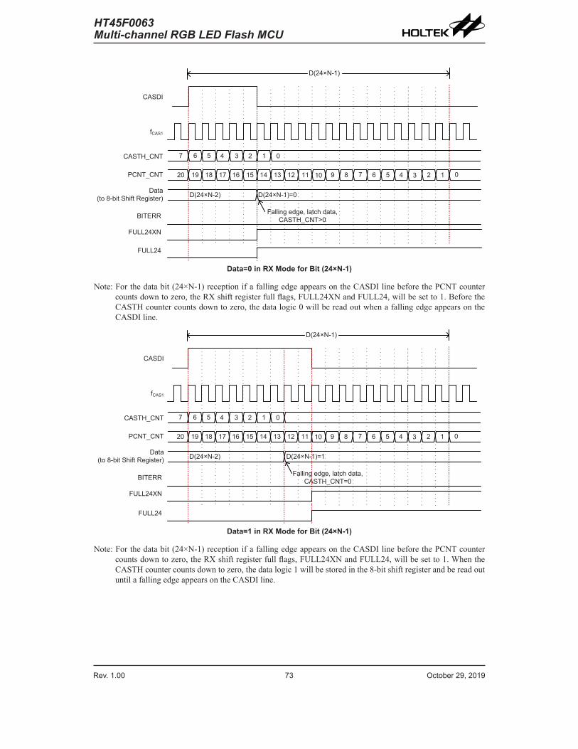
Rev. 1.00 72 October 29, 2019 Rev. 1.00 73 October 29, 2019
HT45F0063Multi-channel RGB LED Flash MCU
HT45F0063Multi-channel RGB LED Flash MCU
D(24×N-1)
CASDI
fCAS1
PCNT_CNT
D(24×N-2)
6 5 4 3CASTH_CNT 7 1 02
19 18 17 1620 1415 13 12 11 10 89 6 457
Falling edge, latch data, CASTH_CNT>0
3 12 0
Data(to 8-bit Shift Register) D(24×N-1)=0
BITERR
FULL24XN
FULL24
Data=0 in RX Mode for Bit (24×N-1)
Note: For the data bit (24×N-1) reception if a falling edge appears on the CASDI line before the PCNT counter counts down to zero, the RX shift register full flags, FULL24XN and FULL24, will be set to 1. Before the CASTH counter counts down to zero, the data logic 0 will be read out when a falling edge appears on the CASDI line.
D(24×N-1)
CASDI
fCAS1
PCNT_CNT
D(24×N-2)
6 5 4 3CASTH_CNT 7 1 02
19 18 17 1620 1415 13 12 11 10 89 6 457
Falling edge, latch data, CASTH_CNT=0
3 12 0
Data(to 8-bit Shift Register) D(24×N-1)=1
BITERR
FULL24XN
FULL24
Data=1 in RX Mode for Bit (24×N-1)
Note: For the data bit (24×N-1) reception if a falling edge appears on the CASDI line before the PCNT counter counts down to zero, the RX shift register full flags, FULL24XN and FULL24, will be set to 1. When the CASTH counter counts down to zero, the data logic 1 will be stored in the 8-bit shift register and be read out until a falling edge appears on the CASDI line.
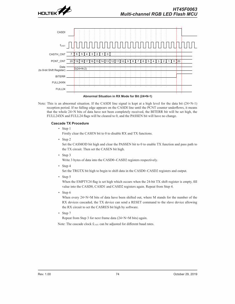
Rev. 1.00 74 October 29, 2019 Rev. 1.00 75 October 29, 2019
HT45F0063Multi-channel RGB LED Flash MCU
HT45F0063Multi-channel RGB LED Flash MCU
CASDI
fCAS1
PCNT_CNT
D(24×N-2)
6 5 4 3CASTH_CNT 7 1 02
19 18 17 1620 1415 13 12 11 10 89 6 457 3 12 0
Data(to 8-bit Shift Register)
BITERR
FULL24XN
20
FULL24
Abnormal Situation in RX Mode for Bit (24×N-1)
Note: This is an abnormal situation. If the CASDI line signal is kept at a high level for the data bit (24×N-1) reception period. If no falling edge appears on the CASDI line until the PCNT counter underflows, it means that the whole 24×N bits of data have not been completely received, the BITERR bit will be set high, the FULL24XN and FULL24 flags will be cleared to 0, and the PASSEN bit will have no change.
Cascade TX Procedure• Step 1
Firstly clear the CASEN bit to 0 to disable RX and TX functions.
• Step 2Set the CASMOD bit high and clear the PASSEN bit to 0 to enable TX function and pass path to the TX circuit. Then set the CASEN bit high.
• Step 3Write 3 bytes of data into the CASD0~CASD2 registers respectively.
• Step 4Set the TRGTX bit high to begin to shift data in the CASD0~CASD2 registers and output.
• Step 5When the EMPTY24 flag is set high which occurs when the 24-bit TX shift register is empty, fill value into the CASD0, CASD1 and CASD2 registers again. Repeat from Step 4.
• Step 6When every 24×N×M bits of data have been shifted out, where M stands for the number of the RX devices cascaded, the TX device can send a RESET command to the slave device allowing the RX circuit to set the CASRES bit high by software.
• Step 7Repeat from Step 3 for next frame data (24×N×M bits) again.
Note: The cascade clock fCAS1 can be adjusted for different baud rates.

Rev. 1.00 74 October 29, 2019 Rev. 1.00 75 October 29, 2019
HT45F0063Multi-channel RGB LED Flash MCU
HT45F0063Multi-channel RGB LED Flash MCU
EMPTY24
TRGTX
CASDO
fCAS1
PCNT_CNT
9 8 7 6D1CNT_CNT 10 4 35
15 14 13 1216 1011 9
2 1 0
45 2 013 16
Dn
8 67
10
Data=1 in TX Mode (n=0~24×N-2, D1CNT=10)
EMPTY24
TRGTX
CASDO
fCAS1
PCNT_CNT
3 2 1 0D0CNT_CNT 4 4
15 14 13 1216 1011 9 45 2 013 16
Dn
8 67
Data=0 in TX Mode (n=0~24×N-2, D0CNT=4)
EMPTY24
TRGTX
CASDO
fCAS1
PCNT_CNT
9 8 7 6D1CNT_CNT 10 4 35
15 14 13 1216 1011 9
2 1 0
45 2 013 16
Dn
8 67
10
Data=1 in TX Mode (n= 24×N-1, D1CNT=10)
Note: The TRGTX bit will be cleared to 0 by hardware when the TX shift register empty flag, EMPTY24, is set high.

Rev. 1.00 76 October 29, 2019 Rev. 1.00 77 October 29, 2019
HT45F0063Multi-channel RGB LED Flash MCU
HT45F0063Multi-channel RGB LED Flash MCU
PWM for RGB LEDThe device includes a PWM function for RGB LED applications, which is composed of four LED PWM modules, two LED RAM buffers and a Register transfer unit as well as an LED COM output unit.
Module 0
Module n
LED Intensity PWMTransfer Unit
fSYS
FDIV[1:0] PWMxDATA(x=0~11 for time-shared scanning,x=0~14 for direct driving)
Divider(/1, /2, /3, /4)
8-bit PWMColor B
8-bit PWMColor A RGB3n
RGB3n+1
RGB3n+2
LED COM Output COMm
8-bit PWMColor C
RAM_Buffer_A RAM_Buffer_B
RAM_SEL
COMOD COMPL
Note: 1. n=0~3 for time-shared scanning mode and direct driving mode, n=4 only for direct driving mode.
2. m=0~3.PWM for RGB LED Block Diagram

Rev. 1.00 76 October 29, 2019 Rev. 1.00 77 October 29, 2019
HT45F0063Multi-channel RGB LED Flash MCU
HT45F0063Multi-channel RGB LED Flash MCU
PWM Register DescriptionOverall operation of the PWM function for RGB LED is controlled using a series of registers. The COM_PWM register is used for PWM function control, PWM clock divider selection, scan mode selection and configuration. The PWM0DATA~PWM14DATA registers are used to define the duty of the PWM outputs.
RegisterName
Bit7 6 5 4 3 2 1 0
COM_PWM PWMEN — FDIV1 FDIV0 RAM_SEL COMPL COMOD SCANMODPWM0DATA D7 D6 D5 D4 D3 D2 D1 D0PWM1DATA D7 D6 D5 D4 D3 D2 D1 D0PWM2DATA D7 D6 D5 D4 D3 D2 D1 D0PWM3DATA D7 D6 D5 D4 D3 D2 D1 D0PWM4DATA D7 D6 D5 D4 D3 D2 D1 D0PWM5DATA D7 D6 D5 D4 D3 D2 D1 D0PWM6DATA D7 D6 D5 D4 D3 D2 D1 D0PWM7DATA D7 D6 D5 D4 D3 D2 D1 D0PWM8DATA D7 D6 D5 D4 D3 D2 D1 D0PWM9DATA D7 D6 D5 D4 D3 D2 D1 D0PWM10DATA D7 D6 D5 D4 D3 D2 D1 D0PWM11DATA D7 D6 D5 D4 D3 D2 D1 D0PWM12DATA D7 D6 D5 D4 D3 D2 D1 D0PWM13DATA D7 D6 D5 D4 D3 D2 D1 D0PWM14DATA D7 D6 D5 D4 D3 D2 D1 D0
PWM Register List
• COM_PWM RegisterBit 7 6 5 4 3 2 1 0
Name PWMEN — FDIV1 FDIV0 RAM_SEL COMPL COMOD SCANMODR/W R/W — R/W R/W R/W R/W R/W R/WPOR 0 — 0 0 0 0 0 0
Bit 7 PWMEN: PWM enable or disable control0: PWM all disable1: PWM all enable
When the PWMEN is set high, the FDIV1~FDIV0, COMPL, COMOD and SCANMOD bits are forbidden to be changed with the exception of the RAM_SEL bit. When the bit is cleared to zero, the COM0~COM3 pins will output inactive data and RGB0~RGB11 are fixed at “1”.
Bit 6 Unimplemented, read as “0”Bit 5~4 FDIV1~FDIV0: PWM clock divider selection
fPWMCLK=00: fSYS clock divided by 101: fSYS clock divided by 210: fSYS clock divided by 311: fSYS clock divided by 4
When these bits are set to “10”, positive half cycle = 2×PWMCLK, negative half cycle = 1×PWMCLK.

Rev. 1.00 78 October 29, 2019 Rev. 1.00 79 October 29, 2019
HT45F0063Multi-channel RGB LED Flash MCU
HT45F0063Multi-channel RGB LED Flash MCU
Bit 3 RAM_SEL: RAM buffer selection for COM scan display (only available for time-shared scanning)
0: Select RAM buffer A for COM scan1: Select RAM buffer B for COM scan
Note that the RAM buffer change only takes effect when the current frame is finished. At the end of the current frame, the RAM_SEL bit value will be captured and the new RAM buffer selection will take effect. In the time-shared scanning mode, general read or write operations to the selected buffer are not available.
Bit 2 COMPL: COM polarity selection (only available for time-shared scanning)0: Low active1: High active
When in the direct driving mode, the COM pins will output inactive data. Pay attention to the COMPL bit setup when in the PWM disable status. If PWMEN=0 and COMPL=0, the COM pins will output a high level (inactive data); if PWMEN=0 and COMPL=1, the COM pins will output a low level (inactive data). It is suggested to first select the COM pins by configuring the pin-shared control bits and configure the COMPL bit before enabling the PWM function.
Bit 1 COMOD: COM mode selection (only available for time-shared scanning)0: 3×COM1: 4×COM
Bit 0 SCANMOD: PWM time-shared scanning or direct driving mode selection 0: Direct driving mode1: Time-shared scanning mode
• PWM0DATA RegisterBit 7 6 5 4 3 2 1 0
Name D7 D6 D5 D4 D3 D2 D1 D0R/W R/W R/W R/W R/W R/W R/W R/W R/WPOR 0 0 0 0 0 0 0 0
Bit 7~0 D7~D0: LED0 color AThis register is read only when in the time-shared scanning mode.
• PWM1DATA RegisterBit 7 6 5 4 3 2 1 0
Name D7 D6 D5 D4 D3 D2 D1 D0R/W R/W R/W R/W R/W R/W R/W R/W R/WPOR 0 0 0 0 0 0 0 0
Bit 7~0 D7~D0: LED0 color BThis register is read only when in the time-shared scanning mode.
• PWM2DATA RegisterBit 7 6 5 4 3 2 1 0
Name D7 D6 D5 D4 D3 D2 D1 D0R/W R/W R/W R/W R/W R/W R/W R/W R/WPOR 0 0 0 0 0 0 0 0
Bit 7~0 D7~D0: LED0 color CThis register is read only when in the time-shared scanning mode.

Rev. 1.00 78 October 29, 2019 Rev. 1.00 79 October 29, 2019
HT45F0063Multi-channel RGB LED Flash MCU
HT45F0063Multi-channel RGB LED Flash MCU
• PWM3DATA RegisterBit 7 6 5 4 3 2 1 0
Name D7 D6 D5 D4 D3 D2 D1 D0R/W R/W R/W R/W R/W R/W R/W R/W R/WPOR 0 0 0 0 0 0 0 0
Bit 7~0 D7~D0: LED1 color AThis register is read only when in the time-shared scanning mode.
• PWM4DATA RegisterBit 7 6 5 4 3 2 1 0
Name D7 D6 D5 D4 D3 D2 D1 D0R/W R/W R/W R/W R/W R/W R/W R/W R/WPOR 0 0 0 0 0 0 0 0
Bit 7~0 D7~D0: LED1 color BThis register is read only when in the time-shared scanning mode.
• PWM5DATA RegisterBit 7 6 5 4 3 2 1 0
Name D7 D6 D5 D4 D3 D2 D1 D0R/W R/W R/W R/W R/W R/W R/W R/W R/WPOR 0 0 0 0 0 0 0 0
Bit 7~0 D7~D0: LED1 color CThis register is read only when in the time-shared scanning mode.
• PWM6DATA RegisterBit 7 6 5 4 3 2 1 0
Name D7 D6 D5 D4 D3 D2 D1 D0R/W R/W R/W R/W R/W R/W R/W R/W R/WPOR 0 0 0 0 0 0 0 0
Bit 7~0 D7~D0: LED2 color AThis register is read only when in the time-shared scanning mode.
• PWM7DATA RegisterBit 7 6 5 4 3 2 1 0
Name D7 D6 D5 D4 D3 D2 D1 D0R/W R/W R/W R/W R/W R/W R/W R/W R/WPOR 0 0 0 0 0 0 0 0
Bit 7~0 D7~D0: LED2 color BThis register is read only when in the time-shared scanning mode.
• PWM8DATA RegisterBit 7 6 5 4 3 2 1 0
Name D7 D6 D5 D4 D3 D2 D1 D0R/W R/W R/W R/W R/W R/W R/W R/W R/WPOR 0 0 0 0 0 0 0 0
Bit 7~0 D7~D0: LED2 color CThis register is read only when in the time-shared scanning mode.
Rev. 1.00 80 October 29, 2019 Rev. 1.00 81 October 29, 2019
HT45F0063Multi-channel RGB LED Flash MCU
HT45F0063Multi-channel RGB LED Flash MCU
• PWM9DATA RegisterBit 7 6 5 4 3 2 1 0
Name D7 D6 D5 D4 D3 D2 D1 D0R/W R/W R/W R/W R/W R/W R/W R/W R/WPOR 0 0 0 0 0 0 0 0
Bit 7~0 D7~D0: LED3 color A This register is read only when in the time-shared scanning mode.
• PWM10DATA RegisterBit 7 6 5 4 3 2 1 0
Name D7 D6 D5 D4 D3 D2 D1 D0R/W R/W R/W R/W R/W R/W R/W R/W R/WPOR 0 0 0 0 0 0 0 0
Bit 7~0 D7~D0: LED3 color BThis register is read only when in the time-shared scanning mode.
• PWM11DATA RegisterBit 7 6 5 4 3 2 1 0
Name D7 D6 D5 D4 D3 D2 D1 D0R/W R/W R/W R/W R/W R/W R/W R/W R/WPOR 0 0 0 0 0 0 0 0
Bit 7~0 D7~D0: LED3 color CThis register is read only when in the time-shared scanning mode.
• PWM12DATA RegisterBit 7 6 5 4 3 2 1 0
Name D7 D6 D5 D4 D3 D2 D1 D0R/W R/W R/W R/W R/W R/W R/W R/W R/WPOR 0 0 0 0 0 0 0 0
Bit 7~0 D7~D0: LED4 color A This register is not available when in the time-shared scanning mode.
• PWM13DATA RegisterBit 7 6 5 4 3 2 1 0
Name D7 D6 D5 D4 D3 D2 D1 D0R/W R/W R/W R/W R/W R/W R/W R/W R/WPOR 0 0 0 0 0 0 0 0
Bit 7~0 D7~D0: LED4 color B This register is not available when in the time-shared scanning mode.
• PWM14DATA RegisterBit 7 6 5 4 3 2 1 0
Name D7 D6 D5 D4 D3 D2 D1 D0R/W R/W R/W R/W R/W R/W R/W R/W R/WPOR 0 0 0 0 0 0 0 0
Bit 7~0 D7~D0: LED4 color C This register is not available when in the time-shared scanning mode.

Rev. 1.00 80 October 29, 2019 Rev. 1.00 81 October 29, 2019
HT45F0063Multi-channel RGB LED Flash MCU
HT45F0063Multi-channel RGB LED Flash MCU
PWM RAM BufferThere are two LED PWM RAM buffers, buffer A and B, with each containing 64 bytes. The buffers are located in Bank 2, 80H~BFH for buffer A and C0H~FFH for buffer B. However, the actual available size for the PWM function is 48 bytes, as shown below. More details regarding the RAM buffer usage will be described in the PWM Operation section.
COM
COM0
COM1
COM2
COM3
RAM_Buffer 00
RAM_Buffer 01
:
RAM_Buffer 11
RAM_Buffer 12
RAM_Buffer 13
:
RAM_Buffer 23
RAM_Buffer 24
RAM_Buffer 25
:
RAM_Buffer 35
RAM_Buffer 36
RAM_Buffer 37
:
RAM_Buffer 47
RAM(Buffer A or B)
Start Address
PWM OperationThe overall PWM function is controlled by the PWMEN bit in the COM_PWM register. If the PWM function is not used, the PWMEN bit should be cleared to disable the PWM function for power saving consideration. During the PWM operations, either in direct driving mode or time-shared scanning mode, if a HALT instruction is executed and the fPWMCLK clock is still on, the PWM operations and waveform output will continue. However, if the fPWMCLK clock is off after executing the HALT instruction, the PWM function will stay in the instantaneous state of entering the HALT status.
The PWM clock is derived from the system clock fSYS and the clock divider used to generate the fPWMCLK clock is selected by the FDIV1~FDIV0 bits.
The PWM function supports two operating modes, which are direct driving mode and time-shared scanning mode, selected by the SCANMOD bit in the COM_PWM register.
Direct Driving ModeIf the direct driving mode is selected by clearing the SCANMOD bit to zero, all of the 4 PWM modules will be used which can drive 15 RGB LEDs. And the output waveform is determined by the LED PWM data registers, PWM0DATA~PWM14DATA. The PWM data register contents, once being changed, will directly react on the RGBn outputs and the RGB dimming will take effect immediately.

Rev. 1.00 82 October 29, 2019 Rev. 1.00 83 October 29, 2019
HT45F0063Multi-channel RGB LED Flash MCU
HT45F0063Multi-channel RGB LED Flash MCU
If the PWM data registers are modified, the PWM function will not be reset to output a new PWM duty cycle but will output the new PWM waveform directly after the old PWM waveform at the moment of data change. It means that the PWM waveforms before and after the data change share the same (256×fPWMCLK) cycle.
In this mode, both RAM buffer A and B can be used as the general purpose data memory and are read/write available.
RGB0
PWM2DATA8-bit B
PWM1DATA8-bit G
PWM0DATA8-bit R
PWM2DATA8-bit B
PWM1DATA8-bit G
PWM0DATA8-bit R
PWM0DATA8-bit R
PWM1DATA8-bit G
PWM2DATA8-bit B
PWM0DATA8-bit R
PWM1DATA8-bit G
PWM2DATA8-bit B
RGB1
RGB2
RGB3
PWM5DATA8-bit B
PWM4DATA8-bit G
PWM3DATA8-bit R
PWM5DATA8-bit B
PWM4DATA8-bit G
PWM3DATA8-bit R
PWM3DATA8-bit R
PWM4DATA8-bit G
PWM5DATA8-bit B
PWM3DATA8-bit R
PWM4DATA8-bit G
PWM5DATA8-bit B
RGB4
RGB5
RGB6
PWM8DATA8-bit B
PWM7DATA8-bit G
PWM6DATA8-bit R
PWM8DATA8-bit B
PWM7DATA8-bit G
PWM6DATA8-bit R
PWM6DATA8-bit R
PWM7DATA8-bit G
PWM8DATA8-bit B
PWM6DATA8-bit R
PWM7DATA8-bit G
PWM8DATA8-bit B
RGB7
RGB8
RGB9
PWM11DATA8-bit B
PWM10DATA8-bit G
PWM9DATA8-bit R
PWM11DATA8-bit B
PWM10DATA8-bit G
PWM9DATA8-bit R
PWM9DATA8-bit R
PWM10DATA8-bit G
PWM11DATA8-bit B
PWM9DATA8-bit R
PWM10DATA8-bit G
PWM11DATA8-bit B
RGB10
RGB11
fDIV
RGB12
PWM14DATA8-bit B
PWM13DATA8-bit G
PWM12DATA8-bit R
PWM14DATA8-bit B
PWM13DATA8-bit G
PWM12DATA8-bit R
PWM12DATA8-bit R
PWM13DATA8-bit G
PWM14DATA8-bit B
PWM12DATA8-bit R
PWM13DATA8-bit G
PWM14DATA8-bit B
RGB13
RGB14
LED PWM Timing for Direct Driving Mode
Rev. 1.00 82 October 29, 2019 Rev. 1.00 83 October 29, 2019
HT45F0063Multi-channel RGB LED Flash MCU
HT45F0063Multi-channel RGB LED Flash MCU
Time-shared Scanning ModeIf the time-shared scanning mode is selected by setting the SCANMOD bit high, only 3 PWM modules will be used to drive 12 RGB LEDs. And the output waveform is determined by the LED PWM data registers, PWM0DATA~PWM11DATA. The PWM12DATA~PWM14DATA registers take no effect in this mode and the corresponding PWM outputs are floating regardless of the register contents.
In this mode, the COM mode, 3×COM or 4×COM, is selected using the COMOD bit and the COM polarity is determined by the COMPL bit. The RAM buffer A or B for COM scan display is determined by the RAM_SEL bit. The 36 bytes (3×COM) or 48 bytes (4×COM) of data in the RAM_Buffer_A/B will be transferred to the PWM0DATA~PWM2DATA & PWM3DATA~ PWM5DATA & PWM6DATA~PWM8DATA & PWM9DATA~PWM11DATA registers by hardware with 12 bytes each time, to generate the corresponding PWM waveforms.
If RAM_SEL is equal to 0, the RAM buffer A is selected and cannot be read or written by the application program, however the RAM buffer B is read/write available. On the contrary, if RAM_SEL is equal to 1, the RAM buffer B is selected and cannot be read or written by the application program, however the RAM buffer A is read/write available. It should be noted that if the RAM buffer selection is changed, the new RAM buffer data will be loaded to the PWM data registers only when the current frame is completed. The unused bytes in the RAM buffer A or B have no effect on the PWM outputs.
The time for loading data from RAM buffer to the PWM data register is:
4×tPWMCLK×12+(0~1)×tPWMCLK+(0~1)×tDIV
The frame cycle for the 3×COM mode is:
3×{[4×tPWMCLK×12+(0~1)×tPWMCLK+(0~1)×tDIV]+256×tDIV}
The frame cycle for the 4×COM mode is:
4×{[4×tPWMCLK×12+(0~1)×tPWMCLK+(0~1)×tDIV]+256×tDIV}

Rev. 1.00 84 October 29, 2019 Rev. 1.00 85 October 29, 2019
HT45F0063Multi-channel RGB LED Flash MCU
HT45F0063Multi-channel RGB LED Flash MCU
COM0 256 tDIV
COM1 256 tDIV
RGB0
256 tDIV
RAM_BUF_028-bit B
RAM_BUF_018-bit G
RAM_BUF_008-bit R
RAM_BUF148-bit B
RAM_BUF_138-bit G
RAM_BUF_128-bit R
RAM_BUF_248-bit R
RAM_BUF_258-bit G
RAM_BUF_268-bit B
RAM_BUF_008-bit R
RAM_BUF_018-bit G
RAM_BUF_028-bit B
RGB1
RGB2
RGB3
RAM_BUF_058-bit B
RAM_BUF_048-bit G
RAM_BUF_038-bit R
RAM_BUF_178-bit B
RAM_BUF_168-bit G
RAM_BUF_158-bit R
RAM_BUF278-bit R
RAM_BUF_288-bit G
RAM_BUF_298-bit B
RAM_BUF_038-bit R
RAM_BUF_048-bit G
RAM_BUF_058-bit B
RGB4
RGB5
RGB6
RAM_BUF_088-bit B
RAM_BUF_078-bit G
RAM_BUF_068-bit R
RAM_BUF_208-bit B
RAM_BUF_198-bit G
RAM_BUF_188-bit R
RAM_BUF_308-bit R
RAM_BUF_318-bit G
RAM_BUF_328-bit B
RAM_BUF_068-bit R
RAM_BUF_078-bit G
RAM_BUF_088-bit B
RGB7
RGB8
fDIV
COM2 256 tDIV
One Frame
Time for loading data from RAM to PWMnDATA
RAM_BUF_118-bit B
RAM_BUF_108-bit G
RAM_BUF_098-bit R
RAM_BUF_238-bit B
RAM_BUF_228-bit G
RAM_BUF_218-bit R
RAM_BUF_338-bit R
RAM_BUF_348-bit G
RAM_BUF_358-bit B
RAM_BUF_098-bit R
RAM_BUF_108-bit G
RAM_BUF_118-bit B
RGB9
RGB10
RGB11
LED PWM Timing for Time-shared Scanning Mode – 3×COM

Rev. 1.00 84 October 29, 2019 Rev. 1.00 85 October 29, 2019
HT45F0063Multi-channel RGB LED Flash MCU
HT45F0063Multi-channel RGB LED Flash MCU
COM1 256 tDIV
COM2 256 tDIV
COM3 256 tDIV
RGB0
RAM_BUF_028-bit B
RAM_BUF_018-bit G
RAM_BUF_008-bit R
RAM_BUF_148-bit B
RAM_BUF_138-bit G
RAM_BUF_128-bit R
RAM_BUF_248-bit R
RAM_BUF_258-bit G
RAM_BUF_268-bit B
RAM_BUF_368-bit R
RAM_BUF_378-bit G
RAM_BUF_388-bit B
RGB1
RGB2
RGB3
RAM_BUF_058-bit B
RAM_BUF_048-bit G
RAM_BUF_038-bit R
RAM_BUF_178-bit B
RAM_BUF_168-bit G
RAM_BUF_158-bit R
RAM_BUF_278-bit R
RAM_BUF_288-bit G
RAM_BUF_298-bit B
RAM_BUF_398-bit R
RAM_BUF_408-bit G
RAM_BUF_418-bit B
RGB4
RGB5
RGB6
RAM_BUF_088-bit B
RAM_BUF_078-bit G
RAM_BUF_068-bit R
RAM_BUF_208-bit B
RAM_BUF_198-bit G
RAM_BUF_188-bit R
RAM_BUF_308-bit R
RAM_BUF_318-bit G
RAM_BUF_328-bit B
RAM_BUF_428-bit R
RAM_BUF_438-bit G
RAM_BUF_448-bit B
RGB7
RGB8
RAM_BUF_008-bit R
RAM_BUF_018-bit G
RAM_BUF_028-bit B
RAM_BUF_038-bit R
RAM_BUF_048-bit G
RAM_BUF_058-bit B
RAM_BUF_068-bit R
RAM_BUF_078-bit G
RAM_BUF_088-bit B
COM0 256 tDIV 256 tDIV
fDIV
One Frame
Time for loading data from RAM to PWMnDATA
RAM_BUF_118-bit B
RAM_BUF_238-bit B
RAM_BUF_358-bit B
RAM_BUF_478-bit B
RAM_BUF_118-bit B
RGB9
RGB10
RGB11
RAM_BUF_098-bit R
RAM_BUF_218-bit R
RAM_BUF_338-bit R
RAM_BUF_458-bit R
RAM_BUF_098-bit R
RAM_BUF_108-bit G
RAM_BUF_228-bit G
RAM_BUF_348-bit G
RAM_BUF_468-bit G
RAM_BUF_108-bit G
LED PWM Timing for Time-shared Scanning Mode – 4×COM

Rev. 1.00 86 October 29, 2019 Rev. 1.00 87 October 29, 2019
HT45F0063Multi-channel RGB LED Flash MCU
HT45F0063Multi-channel RGB LED Flash MCU
Constant Current LED DriverThe device includes an accurate constant current driver which is specifically designed for LED display applications. The device provides 15-channel stable and constant current outputs for driving LEDs.
The output constant current is determined by the current gain selection bits CCG3~CCG0, RGBn PWM input and CCOn pull-high function. The current variation between channels is less than ±5% while the current variation between different devices is less than ±10%. The output current remains constant regardless of the LED forward voltage value.
The constant current can be calculated using the following formula:
ICCOn=3mA×Gain
IOUT Regulatorand DAC
CCOn
Module 0
Module n
RGBn
CCEN
VSS
VDD
CCG[3:0]
VDD
Pull-high Control
PxSnCCEN
CCOnPU
Weak pull-upRPH: shared with I/O pull-high
register
BC[7:0]
ICCON (3mA)
Constant Current LED Driver Block Diagram (CCO only)
IOUT Regulatorand DAC
CCOn/COMm
Module 0
Module n
RGBn
CCEN
VDD
CCG[3:0]
VDD
Pull-high Control
PxSnCCEN
CCOnPU
Weak pull-upRPH: shared with I/O
pull-high register
BC[7:0]
ICCON (3mA)
Switch
COMmOENCOMm_data
COM Driver
VSS
VDD
Constant Current LED Driver Block Diagram (CCO & COM)

Rev. 1.00 86 October 29, 2019 Rev. 1.00 87 October 29, 2019
HT45F0063Multi-channel RGB LED Flash MCU
HT45F0063Multi-channel RGB LED Flash MCU
COMm
COMmOEN
VDD
COM Driver
RPL: pull-low resister
Switch
COMm_data
Constant Current LED Driver Block Diagram (COM only)
Note: 1. n=0~14, m=0~3.2. Module n stands for Module 0 ~ Module 14. 3. RGBn is sourced from the PWMnDATA output.4. COMmOEN is sourced from PBS1 and PCS0.5. COMm_data is sourced from COMm output.
Constant Current LED Driver Block Diagram
Constant Current LED Driver Register DescriptionThere are three control registers associated with the constant current LED driver, CCS, CCOPU0 and CCOPU1. The CCS register is used for constant current function control and gain selection. The CCOPU0 and CCOPU1 registers are used to control the pull-high function of the CCOn pin.
RegisterName
Bit7 6 5 4 3 2 1 0
CCS CCEN D6 D5 D4 CCG3 CCG2 CCG1 CCG0CCOPU0 CCO7PU CCO6PU CCO5PU CCO4PU CCO3PU CCO2PU CCO1PU CCO0PUCCOPU1 — CCO14PU CCO13PU CCO12PU CCO11PU CCO10PU CCO9PU CCO8PUBC BC7 BC6 BC5 BC4 BC3 BC2 BC1 BC0
Constant Current LED Driver Register List
• CCS RegisterBit 7 6 5 4 3 2 1 0
Name CCEN D6 D5 D4 CCG3 CCG2 CCG1 CCG0R/W R/W R/W R/W R/W R/W R/W R/W R/WPOR 0 0 1 0 1 0 1 0
Bit 7 CCEN: Constant Current function enable or disable control0: Disable1: Enable
This bit is used to control the constant current function. When the CCEN bit is cleared to zero, the constant current function will be disabled and the CCOn output will be in a floating state regardless of the RGBn signal. The pull-high resistor shared with the I/O pin cannot be controlled by the CCOnPU bit.

Rev. 1.00 88 October 29, 2019 Rev. 1.00 89 October 29, 2019
HT45F0063Multi-channel RGB LED Flash MCU
HT45F0063Multi-channel RGB LED Flash MCU
When the pin is configured as a CCOn output function and the CCEN bit is set high, the pull-high resistor can be controlled using the corresponding CCOnPU bit. When the RGBn signal is in a logic low state with the CCO function enabled, the CCOn output will be a constant current driver. If the RGBn signal is in a logic high state with the CCO function enabled, the CCOn output will be in a high or floating state depending upon whether the pull-high function is enabled or not.
I/O Mode CCEN RGBn CCOnPU Pull-high Enable/Disable CCOn StatusPx X X X Controlled by PxPU General I/O status CCOn 0 X X Disable Floating
CCOn 1 0 0 Disabled by CCOnPU Output low(constant current)
CCOn 1 0 1 Enabled by CCOnPU Output low (affect constant current value)
CCOn 1 1 0 Disabled by CCOnPU FloatingCCOn 1 1 1 Enabled by CCOnPU Pull-highNote: Px: Port A1 & Port A[7:3] & Port B[7:0] & Port C0; X: Don’t care.
Bit 6~4 D6~D4: Reserved bits. These bits cannot be used and must be fixed as “010”Bit 3~0 CCG3~CCG0: Maximum Constant current gain selection
0000: ICCOn=3mA0001: ICCM=6mA 0010: ICCM=9mA0011: ICCM=12mA0100: ICCM=15mA0101: ICCM=18mA 0110: ICCM=21mA0111: ICCM=24mA1000: ICCM=27mA1001: ICCM=30mA 1010: ICCM=33mA1011: ICCM=36mA1100: ICCM=39mA1101: ICCM=42mA 1110: ICCM=45mA1111: ICCM=48mA
• CCOPU0 RegisterBit 7 6 5 4 3 2 1 0
Name CCO7PU CCO6PU CCO5PU CCO4PU CCO3PU CCO2PU CCO1PU CCO0PUR/W R/W R/W R/W R/W R/W R/W R/W R/WPOR 0 0 0 0 0 0 0 0
Bit 7~0 CCO7PU~CCO0PU: CCO7~CCO0 pull-high control0: Disable1: Enable
• CCOPU1 RegisterBit 7 6 5 4 3 2 1 0
Name — CCO14PU CCO13PU CCO12PU CCO11PU CCO10PU CCO9PU CCO8PUR/W — R/W R/W R/W R/W R/W R/W R/WPOR — 0 0 0 0 0 0 0
Bit 7 Unimplemented, read as “0”Bit 6~0 CCO14PU~CCO8PU: CCO14~CCO8 pull-high control
0: Disable1: Enable
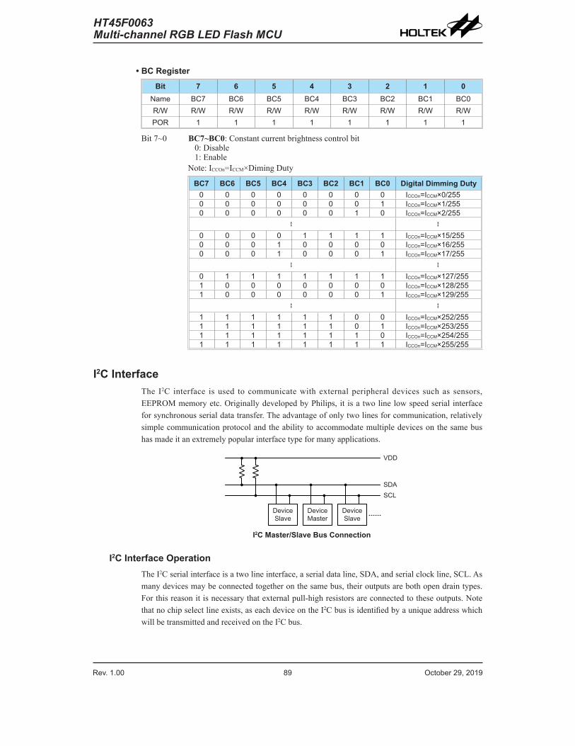
Rev. 1.00 88 October 29, 2019 Rev. 1.00 89 October 29, 2019
HT45F0063Multi-channel RGB LED Flash MCU
HT45F0063Multi-channel RGB LED Flash MCU
• BC RegisterBit 7 6 5 4 3 2 1 0
Name BC7 BC6 BC5 BC4 BC3 BC2 BC1 BC0R/W R/W R/W R/W R/W R/W R/W R/W R/WPOR 1 1 1 1 1 1 1 1
Bit 7~0 BC7~BC0: Constant current brightness control bit0: Disable1: Enable
Note: ICCOn=ICCM×Diming Duty
BC7 BC6 BC5 BC4 BC3 BC2 BC1 BC0 Digital Dimming Duty0 0 0 0 0 0 0 0 ICCOn=ICCM×0/2550 0 0 0 0 0 0 1 ICCOn=ICCM×1/2550 0 0 0 0 0 1 0 ICCOn=ICCM×2/255
-- --
0 0 0 0 1 1 1 1 ICCOn=ICCM×15/2550 0 0 1 0 0 0 0 ICCOn=ICCM×16/2550 0 0 1 0 0 0 1 ICCOn=ICCM×17/255
-- --
0 1 1 1 1 1 1 1 ICCOn=ICCM×127/2551 0 0 0 0 0 0 0 ICCOn=ICCM×128/2551 0 0 0 0 0 0 1 ICCOn=ICCM×129/255
-- --
1 1 1 1 1 1 0 0 ICCOn=ICCM×252/2551 1 1 1 1 1 0 1 ICCOn=ICCM×253/2551 1 1 1 1 1 1 0 ICCOn=ICCM×254/2551 1 1 1 1 1 1 1 ICCOn=ICCM×255/255
I2C InterfaceThe I2C interface is used to communicate with external peripheral devices such as sensors, EEPROM memory etc. Originally developed by Philips, it is a two line low speed serial interface for synchronous serial data transfer. The advantage of only two lines for communication, relatively simple communication protocol and the ability to accommodate multiple devices on the same bus has made it an extremely popular interface type for many applications.
Device Slave
Device Master
DeviceSlave
VDD
SDASCL
I2C Master/Slave Bus Connection
I2C Interface OperationThe I2C serial interface is a two line interface, a serial data line, SDA, and serial clock line, SCL. As many devices may be connected together on the same bus, their outputs are both open drain types. For this reason it is necessary that external pull-high resistors are connected to these outputs. Note that no chip select line exists, as each device on the I2C bus is identified by a unique address which will be transmitted and received on the I2C bus.

Rev. 1.00 90 October 29, 2019 Rev. 1.00 91 October 29, 2019
HT45F0063Multi-channel RGB LED Flash MCU
HT45F0063Multi-channel RGB LED Flash MCU
When two devices communicate with each other on the bidirectional I2C bus, one is known as the master device and one as the slave device. Both master and slave can transmit and receive data, however, it is the master device that has overall control of the bus. For the device, which only operates in slave mode, there are two methods of transferring data on the I2C bus, the slave transmit mode and the slave receive mode.
It is suggested that the device shall not enter the IDLE or SLEEP mode during the I2C communication is in progress.
If the related pin is configured as SDA or SCL function, the pin must be configured to open-collect input/output port and its pull-high function can be enabled by programming the related pull-high control register.
AD Pin
Shift Register
Transmit/Receive
Control Unit
fSYS
fSUB
Data Bus
I2C Address Register(IICA)
I2C Data Register(IICD)
Address Comparator
Read/Write Slave SRW
Detect Start or Stop HBB
Time-outControl
IICTOF
Address Match–HAASI2C Interrupt
Debounce Circuitry
SCL Pin
MUX TXAK
Data out MSB
IICTOEN
Address Match
IICDEB[1:0]
SDA PinData in MSB
Direction ControlHTX
8-bit Data Transfer Complete–HCF
AD Control Circuitry
I2C Block Diagram
START signal from Master
Send slave addressand R/W bit from Master
Acknowledge from slave
Send data byte from Master
Acknowledge from slave
STOP signal from Master
I2C Interface Operation
Rev. 1.00 90 October 29, 2019 Rev. 1.00 91 October 29, 2019
HT45F0063Multi-channel RGB LED Flash MCU
HT45F0063Multi-channel RGB LED Flash MCU
The IICDEB1 and IICDEB0 bits determine the debounce time of the I2C interface. This uses the internal clock to in effect add a debounce time to the external clock to reduce the possibility of glitches on the clock line causing erroneous operation. The debounce time, if selected, can be chosen to be either 2 or 4 system clocks. To achieve the required I2C data transfer speed, there exists a relationship between the system clock, fSYS, and the I2C debounce time. For either the I2C Standard or Fast mode operation, users must take care of the selected system clock frequency and the configured debounce time to match the criterion shown in the following table.
I2C Debounce Time Selection I2C Standard Mode (100kHz) I2C Fast Mode (400kHz)No Debounce fSYS > 2MHz fSYS > 5MHz2 system clock debounce fSYS > 4MHz fSYS > 10MHz4 system clock debounce fSYS > 8MHz fSYS > 20MHz
I2C Minimum fSYS Frequency Requirements
I2C RegistersThere are three control registers associated with the I2C bus, IICC0, IICC1 and IICTOC, one address register IICA and one data register, IICD.
RegisterName
Bit7 6 5 4 3 2 1 0
IICC0 — — — — IICDEB1 IICDEB0 IICEN —IICC1 HCF HAAS HBB HTX TXAK SRW IAMWU RXAKIICD D7 D6 D5 D4 D3 D2 D1 D0IICA IICA6 IICA5 IICA4 IICA3 IICA2 IICA1 IICA0 ADENIICTOC IICTOEN IICTOF IICTOS5 IICTOS4 IICTOS3 IICTOS2 IICTOS1 IICTOS0
I2C Register List
I2C Data RegisterThe IICD register is used to store the data being transmitted and received. Before the device writes data to the I2C bus, the actual data to be transmitted must be placed in the IICD register. After the data is received from the I2C bus, the device can read it from the IICD register. Any transmission or reception of data from the I2C bus must be made via the IICD register.
• IICD RegisterBit 7 6 5 4 3 2 1 0
Name D7 D6 D5 D4 D3 D2 D1 D0R/W R/W R/W R/W R/W R/W R/W R/W R/WPOR x x x x x x x x
“x”: unknownBit 7~0 D7~D0: I2C data register bit 7 ~ bit 0
I2C Address RegisterThe IICA register is the location where the 7-bit slave address of the slave device is stored. The bit7~bit3 of the IICA register define the device slave most significant 5 bits of address. When a master device, which is connected to the I2C bus, sends out an address, which matches the slave address in the IICA register, the slave device will be selected. The least significant 2 bits of address are determined by IICA1~IICA0 or AD pin connection state depending on the ADEN bit of the IICA register.

Rev. 1.00 92 October 29, 2019 Rev. 1.00 93 October 29, 2019
HT45F0063Multi-channel RGB LED Flash MCU
HT45F0063Multi-channel RGB LED Flash MCU
• IICA RegisterBit 7 6 5 4 3 2 1 0
Name IICA6 IICA5 IICA4 IICA3 IICA2 IICA1 IICA0 ADENR/W R/W R/W R/W R/W R/W R/W R/W R/WPOR 0 0 0 0 0 0 0 0
Bit 7~3 IICA6~IICA2: I2C slave address bit7~ bit3IICA6~IICA2 is the I2C slave address bit 6 ~ bit 2.
Bit 2~1 IICA1~IICA0: the least significant I2C slave address bit 1 ~ bit 0ADEN=0, the least significant I2C slave address bit 1~bit 0 are determined by IICA1 and IICA0. The IICA1 and IICA0 can be read and written.ADEN=1, the least significant I2C slave address bit 1~bit 0 is determined by AD pin state IICA1~IIAC0=
00: If the AD pin is connected to VSS01: If the AD pin is connected to SCL10: If the AD pin is connected to SDA11: If the AD pin is connected to VDD
When ADEN=1, the least significant 2 bits of address are determined by AD pin connection state as above. The IICA1 and IICA0 can only be read. The IICA1 and IICA0 can be determined after the falling edge of the second SCL clock from start condition.
Bit 0 ADEN: I2C AD pin control0: Disable AD pin1: Enable AD pin
I2C Control RegistersThere are three control registers for the I2C interface, IICC0, IICC1 and IICTOC. The IICC0 register is used to control the enable/disable function and to set the data transmission clock frequency. The IICC1 register contains the relevant flags which are used to indicate the I2C communication status. Another register, IICTOC, is used to control the I2C time-out function and will be described in the I2C Time-out section.
• IICC0 RegisterBit 7 6 5 4 3 2 1 0
Name — — — — IICDEB1 IICDEB0 IICEN —R/W — — — — R/W R/W R/W —POR — — — — 0 0 0 —
Bit 7~4 Unimplemented, read as “0”Bit 3~2 IICDEB1~IICDEB0: I2C Debounce Time Selection
00: No debounce01: 2 system clock debounce10: 4 system clock debounce11: 4 system clock debounce
Note: If fSYS is come from fH or the bit IAMWU=0, the debounce circuit is effect. Otherwise, SCL and SDA will bypass debounce circuit.
Bit 1 IICEN: I2C Enable Control0: Disable1: Enable
The bit is the overall on/off control for the I2C interface. When the IICEN bit is cleared to zero to disable the I2C interface, the SDA and SCL lines will lose their I2C function and the I2C operating current will be reduced to a minimum value. When the bit is high the I2C interface is enabled. If the IICEN bit changes from low to high, the contents of the I2C control bits such as HTX and TXAK will remain at the previous settings and should therefore be first initialised by the application program while the relevant I2C flags such as HCF, HAAS, HBB, SRW and RXAK will be set to their default states.
Bit 0 Unimplemented, read as “0”

Rev. 1.00 92 October 29, 2019 Rev. 1.00 93 October 29, 2019
HT45F0063Multi-channel RGB LED Flash MCU
HT45F0063Multi-channel RGB LED Flash MCU
• IICC1 RegisterBit 7 6 5 4 3 2 1 0
Name HCF HAAS HBB HTX TXAK SRW IAMWU RXAKR/W R R R R/W R/W R R/W RPOR 1 0 0 0 0 0 0 1
Bit 7 HCF: I2C Bus data transfer completion flag0: Data is being transferred1: Completion of an 8-bit data transfer
This flag will be zero when data is being transferred. Upon completion of an 8-bit data transfer the flag will go high and an interrupt will be generated.
Bit 6 HAAS: I2C Bus address match flag0: Not address match1: Address match
The HAAS flag is the address match flag. This flag is used to determine if the slave device address is the same as the master transmit address. If the addresses match then this bit will be high, if there is no match then the flag will be low.
Bit 5 HBB: I2C Bus busy flag0: I2C Bus is not busy1: I2C Bus is busy
The HBB flag is the I2C busy flag. This flag will be “1” when the I2C bus is busy which will occur when a START signal is detected. The flag will be set to “0” when the bus is free which will occur when a STOP signal is detected.
Bit 4 HTX: I2C slave device is transmitter or receiver selection0: Slave device is the receiver1: Slave device is the transmitter
Bit 3 TXAK: I2C Bus transmit acknowledge flag0: Slave send acknowledge flag1: Slave do not send acknowledge flag
The TXAK bit is the transmit acknowledge flag. After the slave device receipt of 8 bits of data, this bit will be transmitted to the bus on the 9th clock from the slave device. The slave device must always set TXAK bit to “0” before further data is received.
Bit 2 SRW: I2C Slave Read/Write flag0: Slave device should be in receive mode1: Slave device should be in transmit mode
The SRW flag is the I2C Slave Read/Write flag. This flag determines whether the master device wishes to transmit or receive data from the I2C bus. When the transmitted address and slave address is match, that is when the HAAS flag is set high, the slave device will check the SRW flag to determine whether it should be in transmit mode or receive mode. If the SRW flag is high, the master is requesting to read data from the bus, so the slave device should be in transmit mode. When the SRW flag is zero, the master will write data to the bus, therefore the slave device should be in receive mode to read this data.
Bit 1 IAMWU: I2C Address Match Wake-up control0: Disable1: Enable
This bit should be set to 1 to enable the I2C address match wake up from the SLEEP or IDLE Mode. If the IAMWU bit has been set before entering either the SLEEP or IDLE mode to enable the I2C address match wake up, then this bit must be cleared by the application program after wake-up to ensure correction device operation.
Rev. 1.00 94 October 29, 2019 Rev. 1.00 95 October 29, 2019
HT45F0063Multi-channel RGB LED Flash MCU
HT45F0063Multi-channel RGB LED Flash MCU
Bit 0 RXAK: I2C Bus Receive acknowledge flag0: Slave receive acknowledge flag1: Slave does not receive acknowledge flag
The RXAK flag is the receiver acknowledge flag. When the RXAK flag is “0”, it means that a acknowledge signal has been received at the 9th clock, after 8 bits of data have been transmitted. When the slave device in the transmit mode, the slave device checks the RXAK flag to determine if the master receiver wishes to receive the next byte. The slave transmitter will therefore continue sending out data until the RXAK flag is “1”. When this occurs, the slave transmitter will release the SDA line to allow the master to send a STOP signal to release the I2C Bus.
I2C Bus CommunicationCommunication on the I2C bus requires four separate steps, a START signal, a slave device address transmission, a data transmission and finally a STOP signal. When a START signal is placed on the I2C bus, all devices on the bus will receive this signal and be notified of the imminent arrival of data on the bus. The first seven bits of the data will be the slave address with the first bit being the MSB. If the address of the slave device matches that of the transmitted address, the HAAS bit in the IICC1 register will be set and an I2C interrupt will be generated. After entering the interrupt service routine, the slave device must first check the condition of the HAAS and IICTOF bits to determine whether the interrupt source originates from an address match or from the completion of an 8-bit data transfer completion or from the I2C bus time-out occurrence. During a data transfer, note that after the 7-bit slave address has been transmitted, the following bit, which is the 8th bit, is the read/write bit whose value will be placed in the SRW bit. This bit will be checked by the slave device to determine whether to go into transmit or receive mode. Before any transfer of data to or from the I2C bus, the microcontroller must initialise the bus, the following are steps to achieve this:
• Step 1Configure the related pin-shared I/O pins as I2C pin functions. Set the IICEN bits in the IICC0 register to “1” to enable the I2C bus.
• Step 2Set the slave address of the device according to the application requirements.If the AD pin is used, go to Step 3.If the AD pin is unused, go to Step 4.
• Step 3Set the ADEN bit in the IICA register to “1” to enable the AD pin, then connect the AD pin to VDD, VSS, SCL or SDA according to application requirements. Write the most significant 5 bits of the slave address to the IICA6~IICA2 bits of the IICA register, IICA1~IICA0 bit values depend on the AD pin connection state.
• Step 4Clear the ADEN bit in the IICA register to “0” to disable the AD pin. Write the slave address of the device to the IICA6~IICA0 bits of the IICA register.
• Step 5Set the IICE interrupt enable bit of the interrupt control register to enable the I2C interrupt.
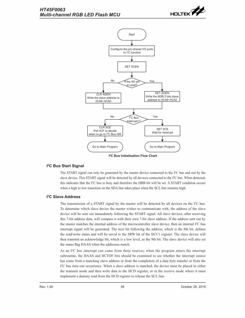
Rev. 1.00 94 October 29, 2019 Rev. 1.00 95 October 29, 2019
HT45F0063Multi-channel RGB LED Flash MCU
HT45F0063Multi-channel RGB LED Flash MCU
Start
SET IICEN
I2C Bus Interrupt=?
CLR IICEPoll IICF to decide
when to go to I2C Bus ISR
SET IICEWait for Interrupt
Go to Main Program Go to Main Program
YesNo
Configure the pin-shared I/O portsto I2C function
YesNo
CLR ADENWrite the slave address to
IICA6~IICA0
If the AD pin is used?
SET ADENWrite the MSB 5 bits slave
address to IICA6~IICA2
I2C Bus Initialisation Flow Chart
I2C Bus Start SignalThe START signal can only be generated by the master device connected to the I2C bus and not by the slave device. This START signal will be detected by all devices connected to the I2C bus. When detected, this indicates that the I2C bus is busy and therefore the HBB bit will be set. A START condition occurs when a high to low transition on the SDA line takes place when the SCL line remains high.
I2C Slave AddressThe transmission of a START signal by the master will be detected by all devices on the I2C bus. To determine which slave device the master wishes to communicate with, the address of the slave device will be sent out immediately following the START signal. All slave devices, after receiving this 7-bit address data, will compare it with their own 7-bit slave address. If the address sent out by the master matches the internal address of the microcontroller slave device, then an internal I2C bus interrupt signal will be generated. The next bit following the address, which is the 8th bit, defines the read/write status and will be saved to the SRW bit of the IICC1 register. The slave device will then transmit an acknowledge bit, which is a low level, as the 9th bit. The slave device will also set the status flag HAAS when the addresses match.
As an I2C bus interrupt can come from three sources, when the program enters the interrupt subroutine, the HAAS and IICTOF bits should be examined to see whether the interrupt source has come from a matching slave address or from the completion of a data byte transfer or from the I2C bus time-out occurrence. When a slave address is matched, the device must be placed in either the transmit mode and then write data to the IICD register, or in the receive mode where it must implement a dummy read from the IICD register to release the SCL line.

Rev. 1.00 96 October 29, 2019 Rev. 1.00 97 October 29, 2019
HT45F0063Multi-channel RGB LED Flash MCU
HT45F0063Multi-channel RGB LED Flash MCU
I2C Bus Read/Write SignalThe SRW bit in the IICC1 register defines whether the master device wishes to read data from the I2C bus or write data to the I2C bus. The slave device should examine this bit to determine if it is to be a transmitter or a receiver. If the SRW flag is “1” then this indicates that the master device wishes to read data from the I2C bus, therefore the slave device must be configured to send data to the I2C bus as a transmitter. If the SRW flag is “0” then this indicates that the master wishes to send data to the I2C bus, therefore the slave device must be configured to read data from the I2C bus as a receiver.
I2C Bus Slave Address Acknowledge SignalAfter the master has transmitted a calling address, any slave device on the I2C bus, whose own internal address matches the calling address, must generate an acknowledge signal. The acknowledge signal will inform the master that a slave device has accepted its calling address. If no acknowledge signal is received by the master then a STOP signal must be transmitted by the master to end the communication. When the HAAS flag is high, the addresses have matched and the slave device must check the SRW flag to determine if it is to be a transmitter or a receiver. If the SRW flag is high, the slave device should be configured to be a transmitter so the HTX bit in the IICC1 register should be set to “1”. If the SRW flag is low, then the microcontroller slave device should be configured as a receiver and the HTX bit in the IICC1 register should be set to “0”.
I2C Bus Data and Acknowledge SignalThe transmitted data is 8-bit wide and is transmitted after the slave device has acknowledged receipt of its slave address. The order of serial bit transmission is the MSB first and the LSB last. After receipt of 8 bits of data, the receiver must transmit an acknowledge signal, level “0”, before it can receive the next data byte. If the slave transmitter does not receive an acknowledge bit signal from the master receiver, then the slave transmitter will release the SDA line to allow the master to send a STOP signal to release the I2C Bus. The corresponding data will be stored in the IICD register. If configured as a transmitter, the slave device must first write the data to be transmitted into the SIMD register. If configured as a receiver, the slave device must read the transmitted data from the IICD register.
When the slave receiver receives the data byte, it must generate an acknowledge bit, known as TXAK, on the 9th clock. The slave device, which is configured as a transmitter will check the RXAK bit in the IICC1 register to determine if it is to send another data byte, if not then it will release the SDA line and await the receipt of a STOP signal from the master.

Rev. 1.00 96 October 29, 2019 Rev. 1.00 97 October 29, 2019
HT45F0063Multi-channel RGB LED Flash MCU
HT45F0063Multi-channel RGB LED Flash MCU
StartSCL
SDA
SCL
SDA
1
S=Start (1 bit)SA=Slave Address (7 bits)SR=SRW bit (1 bit)M=Slave device send acknowledge bit (1 bit)D=Data (8 bits)A=ACK (RXAK bit for transmitter, TXAK bit for receiver, 1 bit)P=Stop (1 bit)
0
ACKSlave Address SRW
StopData ACK
1 1 0 1 0 1 0
1 0 0 1 0 1 0 0
S SA SR M D A D A …… S SA SR M D A D A …… P
I2C Communication Timing Diagram
Note: When a slave address is matched, the device must be placed in either the transmit mode and then write data to the IICD register, or in the receive mode where it must implement a dummy read from the IICD register to release the SCL line.
Start
IICTOF=1?
SET IICTOENCLR IICTOF
RETI
HAAS=1?
HTX=1? SRW=1?
Read from IICD to release SCL Line
RETI
RXAK=1?
Write data to IICD to release SCL Line
CLR HTXCLR TXAK
Dummy read from IICD to release SCL Line RETI
RETI
SET HTX
Write data to IICD to release SCL Line
RETI
CLR HTXCLR TXAK
Dummy read from IICD to release SCL Line
RETI
YesNo
No Yes
Yes NoYesNo
No
Yes
I2C Bus ISR Flow Chart

Rev. 1.00 98 October 29, 2019 Rev. 1.00 99 October 29, 2019
HT45F0063Multi-channel RGB LED Flash MCU
HT45F0063Multi-channel RGB LED Flash MCU
I2C Time-out ControlIn order to reduce the problem of I2C lockup due to reception of erroneous clock sources, a time-out function is provided. If the clock source to the I2C is not received for a while, then the I2C circuitry and registers will be reset after a certain time-out period. The time-out counter starts counting on an I2C bus “START” & “address match” condition, and is cleared by an SCL falling edge. Before the next SCL falling edge arrives, if the time elapsed is greater than the time-out setup by the IICTOC register, then a time-out condition will occur. The time-out function will stop when an I2C “STOP” condition occurs.
StartSCL
SDA
SCL
SDA
1 0
ACKSlave Address SRW
Stop
1 1 0 1 0 1 0
1 0 0 1 0 1 0 0
I2C time-out counter start
I2C time-out counter reset on SCL negative transition
I2C Time-out
When an I2C time-out counter overflow occurs, the counter will stop and the IICTOEN bit will be cleared to zero and the IICTOF bit will be set high to indicate that a time-out condition has occurred. The time-out condition will also generate an interrupt which uses the I2C interrupt vector. When an I2C time-out occurs, the I2C internal circuitry will be reset and the registers will be reset into the following condition:
Registers After I2C Time-outIICD, IICA, IICC0 No changeIICC1 Reset to POR condition
I2C Registers after Time-out
The IICTOF flag can be cleared by the application program. There are 64 time-out periods which can be selected using IICTOS bit field in the IICTOC register. The time-out time is given by the formula:
((1~64)×32)/fSUB
This gives a time-out period which ranges from about 1ms to 64ms.
• IICTOC RegisterBit 7 6 5 4 3 2 1 0
Name IICTOEN IICTOF IICTOS5 IICTOS4 IICTOS3 IICTOS2 IICTOS1 IICTOS0R/W R/W R/W R/W R/W R/W R/W R/W R/WPOR 0 0 0 0 0 0 0 0
Bit 7 IICTOEN: I2C Time-out control0: Disable1: Enable

Rev. 1.00 98 October 29, 2019 Rev. 1.00 99 October 29, 2019
HT45F0063Multi-channel RGB LED Flash MCU
HT45F0063Multi-channel RGB LED Flash MCU
Bit 6 IICTOF: I2C Time-out flag0: No time-out occurred1: Time-out occurred
This bit is set high when time-out occurs and can only be cleared to zero by application program.
Bit 5~0 IICTOS5~IICTOS0: I2C Time-out period selectionI2C time-out clock source is fSUB/32.I2C time-out time is equal to (IICTOS[5:0]+1) × (32/fSUB).
InterruptsInterrupts are an important part of any microcontroller system. When an external event or an internal function such as a Timer Module requires microcontroller attention, the corresponding interrupt will enforce a temporary suspension of the main program allowing the microcontroller to direct attention to the respective need. The device only contains internal interrupts functions. The internal interrupts are generated by various internal functions such as TM, Time Base, I2C interface and cascading transceiver interface.
Interrupt RegistersOverall interrupt control, which basically means the setting of request flags when certain microcontroller conditions occur and the setting of interrupt enable bits by the application program, is controlled by a series of registers, located in the Special Purpose Data Memory, as shown in the accompanying table. The registers fall into two categories. The first is the INTC0~INTC1 registers which configure the primary interrupts, the second is the MFI register which configures the Multi-function interrupt.
Each register contains a number of enable bits to enable or disable individual registers as well as interrupt flags to indicate the presence of an interrupt request. The naming convention of these follows a specific pattern. First is listed an abbreviated interrupt type, then the (optional) number of that interrupt followed by either an “E” for enable/ disable bit or “F” for request flag.
Function Enable Bit Request FlagGlobal EMI —Multi-function MFE MFFTime Base TBE TBFI2C Interface IICE IICFCascading transceiver interface CASINTE CASINTF
CTMCTMPE CTMPFCTMAE CTMAF
Interrupt Register Bit Naming Conventions
Register Name
Bit7 6 5 4 3 2 1 0
INTC0 — CASINTF MFF TBF CASINTE MFE TBE EMIINTC1 — — — IICF — — — IICEMFI — — CTMAF CTMPF — — CTMAE CTMPE
Interrupt Register List

Rev. 1.00 100 October 29, 2019 Rev. 1.00 101 October 29, 2019
HT45F0063Multi-channel RGB LED Flash MCU
HT45F0063Multi-channel RGB LED Flash MCU
• INTC0 RegisterBit 7 6 5 4 3 2 1 0
Name — CASINTF MFF TBF CASINTE MFE TBE EMIR/W — R/W R/W R/W R/W R/W R/W R/WPOR — 0 0 0 0 0 0 0
Bit 7 Unimplemented, read as “0”Bit 6 CASINTF: Cascading transceiver interface interrupt request flag
0: No request1: Interrupt request
Bit 5 MFF: Multi-function interrupt request flag0: No request1: Interrupt request
Bit 4 TBF: Time Base interrupt request flag0: No request1: Interrupt request
Bit 3 CASINTE: Cascading transceiver interface interrupt control0: Disable1: Enable
Bit 2 MFE: Multi-function interrupt control0: Disable1: Enable
Bit 1 TBE: Time Base interrupt control0: Disable1: Enable
Bit 0 EMI: Global interrupt control0: Disable1: Enable
• INTC1 RegisterBit 7 6 5 4 3 2 1 0
Name — — — IICF — — — IICER/W — — — R/W — — — R/WPOR — — — 0 — — — 0
Bit 7~5 Unimplemented, read as “0”Bit 4 IICF: I2C interface interrupt request flag
0: No request1: Interrupt request
Bit 3~1 Unimplemented, read as “0”Bit 0 IICE: I2C interface interrupt control
0: Disable1: Enable

Rev. 1.00 100 October 29, 2019 Rev. 1.00 101 October 29, 2019
HT45F0063Multi-channel RGB LED Flash MCU
HT45F0063Multi-channel RGB LED Flash MCU
• MFI RegisterBit 7 6 5 4 3 2 1 0
Name — — CTMAF CTMPF — — CTMAE CTMPER/W — — R/W R/W — — R/W R/WPOR — — 0 0 — — 0 0
Bit 7~6 Unimplemented, read as “0”Bit 5 CTMAF: CTM Comparator A match interrupt request flag
0: No request1: Interrupt request
Bit 4 CTMPF: CTM Comparator P match interrupt request flag0: No request1: Interrupt request
Bit 3~2 Unimplemented, read as “0”Bit 1 CTMAE: CTM Comparator A match interrupt control
0: Disable1: Enable
Bit 0 CTMPE: CTM Comparator P match interrupt control0: Disable1: Enable
Interrupt OperationWhen the conditions for an interrupt event occur, such as a TM Comparator P or Comparator A match etc., the relevant interrupt request flag will be set. Whether the request flag actually generates a program jump to the relevant interrupt vector is determined by the condition of the interrupt enable bit. If the enable bit is set high then the program will jump to its relevant vector, if the enable bit is zero then although the interrupt request flag is set an actual interrupt will not be generated and the program will not jump to the relevant interrupt vector. The global interrupt enable bit, if cleared to zero, will disable all interrupts.
When an interrupt is generated, the Program Counter, which stores the address of the next instruction to be executed, will be transferred onto the stack. The Program Counter will then be loaded with a new address which will be the value of the corresponding interrupt vector. The microcontroller will then fetch its next instruction from this interrupt vector. The instruction at this vector will usually be a “JMP” which will jump to another section of program which is known as the interrupt service routine. Here is located the code to control the appropriate interrupt. The interrupt service routine must be terminated with a “RETI”, which retrieves the original Program Counter address from the stack and allows the microcontroller to continue with normal execution at the point where the interrupt occurred.
The various interrupt enable bits, together with their associated request flags, are shown in the Accompanying diagrams with their order of priority. Some interrupt sources have their own individual vector while others share the same multi-function interrupt vector. Once an interrupt subroutine is serviced, all the other interrupts will be blocked, as the global interrupt enable bit, EMI bit will be cleared automatically. This will prevent any further interrupt nesting from occurring. However, if other interrupt requests occur during this interval, although the interrupt will not be immediately serviced, the request flag will still be recorded.
If an interrupt requires immediate servicing while the program is already in another interrupt service routine, the EMI bit should be set after entering the routine, to allow interrupt nesting. If the stack is full, the interrupt request will not be acknowledged, even if the related interrupt is enabled, until the Stack Pointer is decremented. If immediate service is desired, the stack must be prevented from
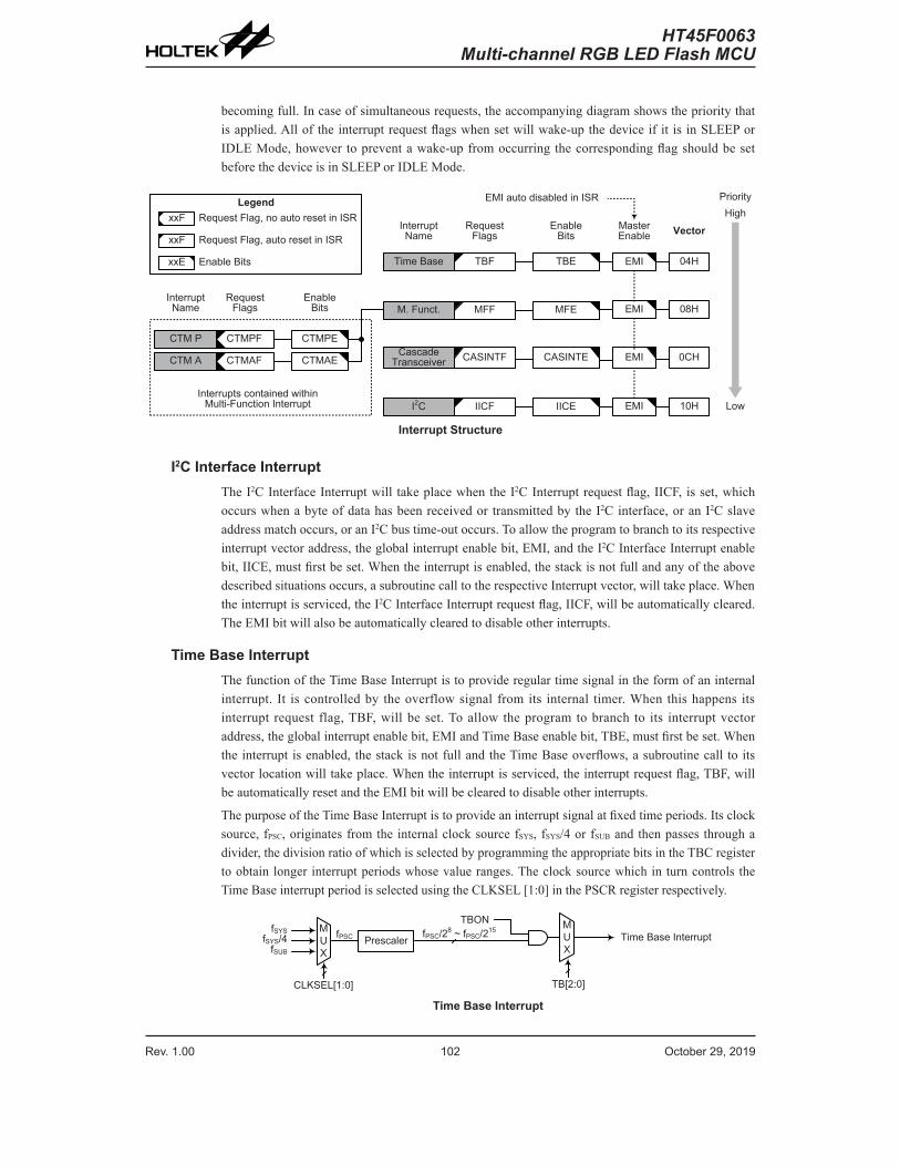
Rev. 1.00 102 October 29, 2019 Rev. 1.00 103 October 29, 2019
HT45F0063Multi-channel RGB LED Flash MCU
HT45F0063Multi-channel RGB LED Flash MCU
becoming full. In case of simultaneous requests, the accompanying diagram shows the priority that is applied. All of the interrupt request flags when set will wake-up the device if it is in SLEEP or IDLE Mode, however to prevent a wake-up from occurring the corresponding flag should be set before the device is in SLEEP or IDLE Mode.
Interrupt Name
Request Flags
Enable Bits
Master Enable Vector
EMI auto disabled in ISR PriorityHigh
LowInterrupts contained within
Multi-Function Interrupt
xxE Enable Bits
xxF Request Flag, auto reset in ISR
LegendxxF Request Flag, no auto reset in ISR
M. Funct. MFF MFE EMI 08H
CTM P CTMPF CTMPE
CTM A CTMAF CTMAE
04HEMI
CascadeTransceiver CASINTF CASINTE EMI 0CH
Interrupt Name
Request Flags
Enable Bits
Time Base TBF TBE
EMII2C IICF IICE 10H
Interrupt Structure
I2C Interface InterruptThe I2C Interface Interrupt will take place when the I2C Interrupt request flag, IICF, is set, which occurs when a byte of data has been received or transmitted by the I2C interface, or an I2C slave address match occurs, or an I2C bus time-out occurs. To allow the program to branch to its respective interrupt vector address, the global interrupt enable bit, EMI, and the I2C Interface Interrupt enable bit, IICE, must first be set. When the interrupt is enabled, the stack is not full and any of the above described situations occurs, a subroutine call to the respective Interrupt vector, will take place. When the interrupt is serviced, the I2C Interface Interrupt request flag, IICF, will be automatically cleared. The EMI bit will also be automatically cleared to disable other interrupts.
Time Base InterruptThe function of the Time Base Interrupt is to provide regular time signal in the form of an internal interrupt. It is controlled by the overflow signal from its internal timer. When this happens its interrupt request flag, TBF, will be set. To allow the program to branch to its interrupt vector address, the global interrupt enable bit, EMI and Time Base enable bit, TBE, must first be set. When the interrupt is enabled, the stack is not full and the Time Base overflows, a subroutine call to its vector location will take place. When the interrupt is serviced, the interrupt request flag, TBF, will be automatically reset and the EMI bit will be cleared to disable other interrupts.
The purpose of the Time Base Interrupt is to provide an interrupt signal at fixed time periods. Its clock source, fPSC, originates from the internal clock source fSYS, fSYS/4 or fSUB and then passes through a divider, the division ratio of which is selected by programming the appropriate bits in the TBC register to obtain longer interrupt periods whose value ranges. The clock source which in turn controls the Time Base interrupt period is selected using the CLKSEL [1:0] in the PSCR register respectively.
fSYS/4fSYS
fSUB
MUX
Prescaler
CLKSEL[1:0]
fPSC fPSC/28 ~ fPSC/215 MUX
TB[2:0]
Time Base InterruptTBON
Time Base Interrupt

Rev. 1.00 102 October 29, 2019 Rev. 1.00 103 October 29, 2019
HT45F0063Multi-channel RGB LED Flash MCU
HT45F0063Multi-channel RGB LED Flash MCU
• PSCR RegisterBit 7 6 5 4 3 2 1 0
Name — — — — — — CLKSEL1 CLKSEL0R/W — — — — — — R/W R/WPOR — — — — — — 0 0
Bit 7~2 Unimplemented, read as “0”Bit 1~0 CLKSEL1~CLKSEL0: Prescaler clock source selection
00: fSYS
01: fSYS/41x: fSUB
• TBC RegisterBit 7 6 5 4 3 2 1 0
Name TBON — — — — TB2 TB1 TB0R/W R/W — — — — R/W R/W R/WPOR 0 — — — — 0 0 0
Bit 7 TBON: Time Base Enable Control0: Disable1: Enable
Bit 6~3 Unimplemented, read as “0”Bit 2~0 TB2~TB0: Time Base time-out period selection
000: 28/fPSC
001: 29/fPSC
010: 210/fPSC
011: 211/fPSC
100: 212/fPSC
101: 213/fPSC
110: 214/fPSC
111: 215/fPSC
Multi-function InterruptWithin the device there is a Multi-function interrupt. Unlike the other independent interrupts, the interrupt has no independent source, but rather are formed from other existing interrupt sources, namely the TM interrupts.
A Multi-function interrupt request will take place when any of the Multi-function interrupt request flag MFF is set. The Multi-function interrupt flag will be set when any of their included functions generate an interrupt request flag. To allow the program to branch to its respective interrupt vector address, when the Multi-function interrupt is enabled and the stack is not full, and any one of the interrupts contained within the Multi-function interrupt occurs, a subroutine call to the Multi-function interrupt vector will take place. When the interrupt is serviced, the related Multi-function request flag will be automatically reset and the EMI bit will be automatically cleared to disable other interrupts.
However, it must be noted that, although the Multi-function Interrupt request flag will be automatically reset when the interrupt is serviced, the request flags from the original source of the Multi-function interrupt will not be automatically reset and must be manually reset by the application program.

Rev. 1.00 104 October 29, 2019 Rev. 1.00 105 October 29, 2019
HT45F0063Multi-channel RGB LED Flash MCU
HT45F0063Multi-channel RGB LED Flash MCU
Cascade Transceiver Interface InterruptA Cascade Transceiver Interface Interrupt request will take place when the Cascade Transceiver Interface Interrupt request flag, CASINTF, is set, which occurs when RX receive data format error occurs, cascade circuit reset occurs, cascading transceiver TX shift register is empty or cascading transceiver 24 bits or 24×N bits RX shift register is full. To allow the program to branch to its respective interrupt vector address, the global interrupt enable bit, EMI, and the Cascade Transceiver Interface Interrupt enable bit, CASINTE, must first be set. When the interrupt is enabled, the stack is not full and any one of the above four described situations occurs, a subroutine call to the respective Interrupt vector, will take place. When the Cascade Transceiver Interface Interrupt is serviced, the interrupt request flag, CASINTF, will be automatically reset and the EMI bit will be cleared to disable other interrupts.
Timer Module Interrupts The CTM has two interrupts which are both contained within the Multi-function Interrupt. For the CTM there are two interrupt request flags CTMPF and CTMAF and two enable bits CTMPE and CTMAE. A CTM interrupt request will take place when any of the CTM request flags is set, a situation which occurs when a CTM comparator P or comparator A match situation happens.
To allow the program to branch to its respective interrupt vector address, the global interrupt enable bit, EMI, and the respective CTM Interrupt enable bit, and the associated Multi-function interrupt enable bit, MFE, must first be set. When the interrupt is enabled, the stack is not full and a CTM comparator match situation occurs, a subroutine call to the relevant CTM Interrupt vector locations, will take place. When the CTM interrupt is serviced, the EMI bit will be automatically cleared to disable other interrupts, however only the related MFF flag will be automatically cleared. As the CTM interrupt request flags will not be automatically cleared, they have to be cleared by the application program.
Interrupt Wake-up FunctionEach of the interrupt functions has the capability of waking up the microcontroller when in the SLEEP or IDLE Mode. A wake-up is generated when an interrupt request flag changes from low to high and is independent of whether the interrupt is enabled or not. Care must therefore be taken if spurious wake-up situations are to be avoided. If an interrupt wake-up function is to be disabled then the corresponding interrupt request flag should be set high before the device enters the SLEEP or IDLE Mode. The interrupt enable bits have no effect on the interrupt wake-up function.
Programming ConsiderationsBy disabling the relevant interrupt enable bits, a requested interrupt can be prevented from being serviced, however, once an interrupt request flag is set, it will remain in this condition in the interrupt register until the corresponding interrupt is serviced or until the request flag is cleared by the application program.
Where a certain interrupt is contained within a Multi-function interrupt, then when the interrupt service routine is executed, as only the Multi-function interrupt request flags, MFF, will be automatically cleared, the individual request flag for the function needs to be cleared by the application program.
It is recommended that programs do not use the “CALL” instruction within the interrupt service subroutine. Interrupts often occur in an unpredictable manner or need to be serviced immediately. If only one stack is left and the interrupt is not well controlled, the original control sequence will be damaged once a CALL subroutine is executed in the interrupt subroutine.
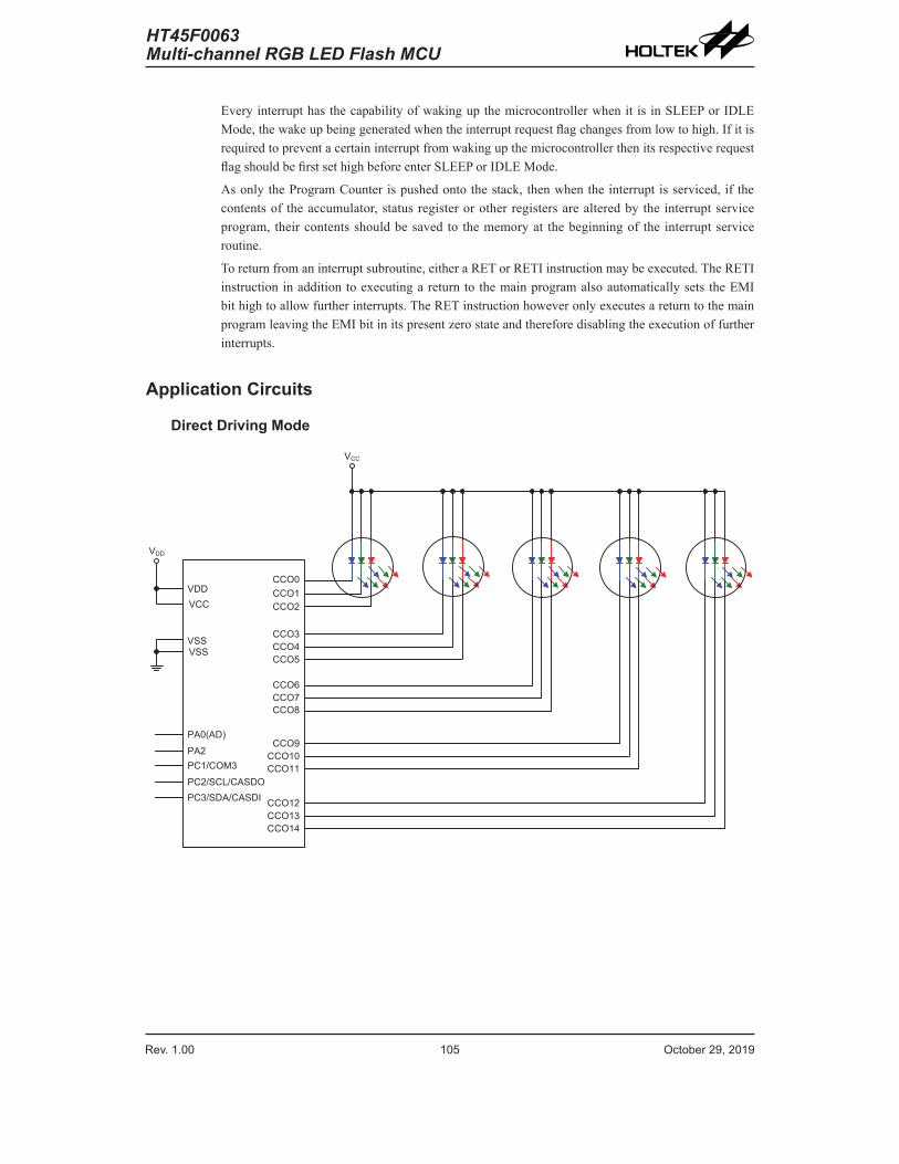
Rev. 1.00 104 October 29, 2019 Rev. 1.00 105 October 29, 2019
HT45F0063Multi-channel RGB LED Flash MCU
HT45F0063Multi-channel RGB LED Flash MCU
Every interrupt has the capability of waking up the microcontroller when it is in SLEEP or IDLE Mode, the wake up being generated when the interrupt request flag changes from low to high. If it is required to prevent a certain interrupt from waking up the microcontroller then its respective request flag should be first set high before enter SLEEP or IDLE Mode.
As only the Program Counter is pushed onto the stack, then when the interrupt is serviced, if the contents of the accumulator, status register or other registers are altered by the interrupt service program, their contents should be saved to the memory at the beginning of the interrupt service routine.
To return from an interrupt subroutine, either a RET or RETI instruction may be executed. The RETI instruction in addition to executing a return to the main program also automatically sets the EMI bit high to allow further interrupts. The RET instruction however only executes a return to the main program leaving the EMI bit in its present zero state and therefore disabling the execution of further interrupts.
Application Circuits
Direct Driving Mode
VDD
PA0(AD)
VDD
VSS
VCC
CCO0CCO1CCO2
CCO3CCO4CCO5
CCO6CCO7CCO8
CCO9CCO10CCO11
PA2
CCO12CCO13CCO14
VCC
VSS
PC1/COM3
PC2/SCL/CASDOPC3/SDA/CASDI

Rev. 1.00 106 October 29, 2019 Rev. 1.00 107 October 29, 2019
HT45F0063Multi-channel RGB LED Flash MCU
HT45F0063Multi-channel RGB LED Flash MCU
Time-shared Scanning Mode – 3×COM
VDD
VDD
VSS
CCO0CCO1
CCO2
CCO3CCO4
CCO5
CCO6CCO7
CCO8
COM0
COM1
COM2
PA0(AD)
PA2
CCO9CCO10
CCO11
VCC
VSS
PC1/COM3
PC2/SCL/CASDO
PC3/SDA/CASDI

Rev. 1.00 106 October 29, 2019 Rev. 1.00 107 October 29, 2019
HT45F0063Multi-channel RGB LED Flash MCU
HT45F0063Multi-channel RGB LED Flash MCU
Time-shared Scanning Mode – 4×COM
CCO0
CCO1
CCO2
CCO3
CCO4
CCO5
CCO6
CCO7
CCO8
COM1
COM2
COM3
COM0VDD
VDD
VSS
PA0(AD)
CCO9
CCO10
CCO11
VCC
VSS
PA2
PC2/SCL/CASDO
PC3/SDA/CASDI
Rev. 1.00 108 October 29, 2019 Rev. 1.00 109 October 29, 2019
HT45F0063Multi-channel RGB LED Flash MCU
HT45F0063Multi-channel RGB LED Flash MCU
Instruction Set
IntroductionCentral to the successful operation of any microcontroller is its instruction set, which is a set of program instruction codes that directs the microcontroller to perform certain operations. In the case of Holtek microcontroller, a comprehensive and flexible set of over 60 instructions is provided to enable programmers to implement their application with the minimum of programming overheads.
For easier understanding of the various instruction codes, they have been subdivided into several functional groupings.
Instruction TimingMost instructions are implemented within one instruction cycle. The exceptions to this are branch, call, or table read instructions where two instruction cycles are required. One instruction cycle is equal to 4 system clock cycles, therefore in the case of an 8MHz system oscillator, most instructions would be implemented within 0.5μs and branch or call instructions would be implemented within 1μs. Although instructions which require one more cycle to implement are generally limited to the JMP, CALL, RET, RETI and table read instructions, it is important to realize that any other instructions which involve manipulation of the Program Counter Low register or PCL will also take one more cycle to implement. As instructions which change the contents of the PCL will imply a direct jump to that new address, one more cycle will be required. Examples of such instructions would be "CLR PCL" or "MOV PCL, A". For the case of skip instructions, it must be noted that if the result of the comparison involves a skip operation then this will also take one more cycle, if no skip is involved then only one cycle is required.
Moving and Transferring DataThe transfer of data within the microcontroller program is one of the most frequently used operations. Making use of three kinds of MOV instructions, data can be transferred from registers to the Accumulator and vice-versa as well as being able to move specific immediate data directly into the Accumulator. One of the most important data transfer applications is to receive data from the input ports and transfer data to the output ports.
Arithmetic OperationsThe ability to perform certain arithmetic operations and data manipulation is a necessary feature of most microcontroller applications. Within the Holtek microcontroller instruction set are a range of add and subtract instruction mnemonics to enable the necessary arithmetic to be carried out. Care must be taken to ensure correct handling of carry and borrow data when results exceed 255 for addition and less than 0 for subtraction. The increment and decrement instructions INC, INCA, DEC and DECA provide a simple means of increasing or decreasing by a value of one of the values in the destination specified.
Rev. 1.00 108 October 29, 2019 Rev. 1.00 109 October 29, 2019
HT45F0063Multi-channel RGB LED Flash MCU
HT45F0063Multi-channel RGB LED Flash MCU
Logical and Rotate OperationThe standard logical operations such as AND, OR, XOR and CPL all have their own instruction within the Holtek microcontroller instruction set. As with the case of most instructions involving data manipulation, data must pass through the Accumulator which may involve additional programming steps. In all logical data operations, the zero flag may be set if the result of the operation is zero. Another form of logical data manipulation comes from the rotate instructions such as RR, RL, RRC and RLC which provide a simple means of rotating one bit right or left. Different rotate instructions exist depending on program requirements. Rotate instructions are useful for serial port programming applications where data can be rotated from an internal register into the Carry bit from where it can be examined and the necessary serial bit set high or low. Another application which rotate data operations are used is to implement multiplication and division calculations.
Branches and Control TransferProgram branching takes the form of either jumps to specified locations using the JMP instruction or to a subroutine using the CALL instruction. They differ in the sense that in the case of a subroutine call, the program must return to the instruction immediately when the subroutine has been carried out. This is done by placing a return instruction "RET" in the subroutine which will cause the program to jump back to the address right after the CALL instruction. In the case of a JMP instruction, the program simply jumps to the desired location. There is no requirement to jump back to the original jumping off point as in the case of the CALL instruction. One special and extremely useful set of branch instructions are the conditional branches. Here a decision is first made regarding the condition of a certain data memory or individual bits. Depending upon the conditions, the program will continue with the next instruction or skip over it and jump to the following instruction. These instructions are the key to decision making and branching within the program perhaps determined by the condition of certain input switches or by the condition of internal data bits.
Bit OperationsThe ability to provide single bit operations on Data Memory is an extremely flexible feature of all Holtek microcontrollers. This feature is especially useful for output port bit programming where individual bits or port pins can be directly set high or low using either the "SET [m].i" or "CLR [m].i" instructions respectively. The feature removes the need for programmers to first read the 8-bit output port, manipulate the input data to ensure that other bits are not changed and then output the port with the correct new data. This read-modify-write process is taken care of automatically when these bit operation instructions are used.
Table Read OperationsData storage is normally implemented by using registers. However, when working with large amounts of fixed data, the volume involved often makes it inconvenient to store the fixed data in the Data Memory. To overcome this problem, Holtek microcontrollers allow an area of Program Memory to be set as a table where data can be directly stored. A set of easy to use instructions provides the means by which this fixed data can be referenced and retrieved from the Program Memory.
Other OperationsIn addition to the above functional instructions, a range of other instructions also exist such as the "HALT" instruction for Power-down operations and instructions to control the operation of the Watchdog Timer for reliable program operations under extreme electric or electromagnetic environments. For their relevant operations, refer to the functional related sections.

Rev. 1.00 110 October 29, 2019 Rev. 1.00 111 October 29, 2019
HT45F0063Multi-channel RGB LED Flash MCU
HT45F0063Multi-channel RGB LED Flash MCU
Instruction Set SummaryThe following table depicts a summary of the instruction set categorised according to function and can be consulted as a basic instruction reference using the following listed conventions.
Table Conventionsx: Bits immediate data m: Data Memory address A: Accumulator i: 0~7 number of bits addr: Program memory address
Mnemonic Description Cycles Flag AffectedArithmeticADD A,[m] Add Data Memory to ACC 1 Z, C, AC, OVADDM A,[m] Add ACC to Data Memory 1Note Z, C, AC, OVADD A,x Add immediate data to ACC 1 Z, C, AC, OVADC A,[m] Add Data Memory to ACC with Carry 1 Z, C, AC, OVADCM A,[m] Add ACC to Data memory with Carry 1Note Z, C, AC, OVSUB A,x Subtract immediate data from the ACC 1 Z, C, AC, OVSUB A,[m] Subtract Data Memory from ACC 1 Z, C, AC, OVSUBM A,[m] Subtract Data Memory from ACC with result in Data Memory 1Note Z, C, AC, OVSBC A,[m] Subtract Data Memory from ACC with Carry 1 Z, C, AC, OVSBCM A,[m] Subtract Data Memory from ACC with Carry, result in Data Memory 1Note Z, C, AC, OVDAA [m] Decimal adjust ACC for Addition with result in Data Memory 1Note CLogic OperationAND A,[m] Logical AND Data Memory to ACC 1 ZOR A,[m] Logical OR Data Memory to ACC 1 ZXOR A,[m] Logical XOR Data Memory to ACC 1 ZANDM A,[m] Logical AND ACC to Data Memory 1Note ZORM A,[m] Logical OR ACC to Data Memory 1Note ZXORM A,[m] Logical XOR ACC to Data Memory 1Note ZAND A,x Logical AND immediate Data to ACC 1 ZOR A,x Logical OR immediate Data to ACC 1 ZXOR A,x Logical XOR immediate Data to ACC 1 ZCPL [m] Complement Data Memory 1Note ZCPLA [m] Complement Data Memory with result in ACC 1 ZIncrement & DecrementINCA [m] Increment Data Memory with result in ACC 1 ZINC [m] Increment Data Memory 1Note ZDECA [m] Decrement Data Memory with result in ACC 1 ZDEC [m] Decrement Data Memory 1Note ZRotateRRA [m] Rotate Data Memory right with result in ACC 1 NoneRR [m] Rotate Data Memory right 1Note NoneRRCA [m] Rotate Data Memory right through Carry with result in ACC 1 CRRC [m] Rotate Data Memory right through Carry 1Note CRLA [m] Rotate Data Memory left with result in ACC 1 NoneRL [m] Rotate Data Memory left 1Note NoneRLCA [m] Rotate Data Memory left through Carry with result in ACC 1 CRLC [m] Rotate Data Memory left through Carry 1Note C

Rev. 1.00 110 October 29, 2019 Rev. 1.00 111 October 29, 2019
HT45F0063Multi-channel RGB LED Flash MCU
HT45F0063Multi-channel RGB LED Flash MCU
Mnemonic Description Cycles Flag AffectedData MoveMOV A,[m] Move Data Memory to ACC 1 NoneMOV [m],A Move ACC to Data Memory 1Note NoneMOV A,x Move immediate data to ACC 1 NoneBit OperationCLR [m].i Clear bit of Data Memory 1Note NoneSET [m].i Set bit of Data Memory 1Note NoneBranch OperationJMP addr Jump unconditionally 2 NoneSZ [m] Skip if Data Memory is zero 1Note NoneSZA [m] Skip if Data Memory is zero with data movement to ACC 1Note NoneSZ [m].i Skip if bit i of Data Memory is zero 1Note NoneSNZ [m].i Skip if bit i of Data Memory is not zero 1Note NoneSIZ [m] Skip if increment Data Memory is zero 1Note NoneSDZ [m] Skip if decrement Data Memory is zero 1Note NoneSIZA [m] Skip if increment Data Memory is zero with result in ACC 1Note NoneSDZA [m] Skip if decrement Data Memory is zero with result in ACC 1Note NoneCALL addr Subroutine call 2 NoneRET Return from subroutine 2 NoneRET A,x Return from subroutine and load immediate data to ACC 2 NoneRETI Return from interrupt 2 NoneTable Read OperationTABRD [m] Read table (specific page or current page) to TBLH and Data Memory 2Note NoneTABRDL [m] Read table (last page) to TBLH and Data Memory 2Note NoneMiscellaneousNOP No operation 1 NoneCLR [m] Clear Data Memory 1Note NoneSET [m] Set Data Memory 1Note NoneCLR WDT Clear Watchdog Timer 1 TO, PDFCLR WDT1 Pre-clear Watchdog Timer 1 TO, PDFCLR WDT2 Pre-clear Watchdog Timer 1 TO, PDFSWAP [m] Swap nibbles of Data Memory 1Note NoneSWAPA [m] Swap nibbles of Data Memory with result in ACC 1 NoneHALT Enter power down mode 1 TO, PDF
Note: 1. For skip instructions, if the result of the comparison involves a skip then up to two cycles are required, if no skip takes place only one cycle is required.
2. Any instruction which changes the contents of the PCL will also require 2 cycles for execution.3. For the "CLR WDT1" and "CLR WDT2" instructions the TO and PDF flags may be affected by the
execution status. The TO and PDF flags are cleared after both "CLR WDT1" and "CLR WDT2" instructions are consecutively executed. Otherwise the TO and PDF flags remain unchanged.

Rev. 1.00 112 October 29, 2019 Rev. 1.00 113 October 29, 2019
HT45F0063Multi-channel RGB LED Flash MCU
HT45F0063Multi-channel RGB LED Flash MCU
Instruction Definition
ADC A,[m] Add Data Memory to ACC with CarryDescription The contents of the specified Data Memory, Accumulator and the carry flag are added. The result is stored in the Accumulator.Operation ACC ← ACC + [m] + CAffected flag(s) OV, Z, AC, C
ADCM A,[m] Add ACC to Data Memory with CarryDescription The contents of the specified Data Memory, Accumulator and the carry flag are added. The result is stored in the specified Data Memory.Operation [m] ← ACC + [m] + CAffected flag(s) OV, Z, AC, C
ADD A,[m] Add Data Memory to ACCDescription The contents of the specified Data Memory and the Accumulator are added. The result is stored in the Accumulator.Operation ACC ← ACC + [m]Affected flag(s) OV, Z, AC, C
ADD A,x Add immediate data to ACCDescription The contents of the Accumulator and the specified immediate data are added. The result is stored in the Accumulator.Operation ACC ← ACC + xAffected flag(s) OV, Z, AC, C
ADDM A,[m] Add ACC to Data MemoryDescription The contents of the specified Data Memory and the Accumulator are added. The result is stored in the specified Data Memory.Operation [m] ← ACC + [m]Affected flag(s) OV, Z, AC, C
AND A,[m] Logical AND Data Memory to ACCDescription Data in the Accumulator and the specified Data Memory perform a bitwise logical AND operation. The result is stored in the Accumulator.Operation ACC ← ACC ″AND″ [m]Affected flag(s) Z
AND A,x Logical AND immediate data to ACCDescription Data in the Accumulator and the specified immediate data perform a bit wise logical AND operation. The result is stored in the Accumulator.Operation ACC ← ACC ″AND″ xAffected flag(s) Z
ANDM A,[m] Logical AND ACC to Data MemoryDescription Data in the specified Data Memory and the Accumulator perform a bitwise logical AND operation. The result is stored in the Data Memory.Operation [m] ← ACC ″AND″ [m]Affected flag(s) Z

Rev. 1.00 112 October 29, 2019 Rev. 1.00 113 October 29, 2019
HT45F0063Multi-channel RGB LED Flash MCU
HT45F0063Multi-channel RGB LED Flash MCU
CALL addr Subroutine callDescription Unconditionally calls a subroutine at the specified address. The Program Counter then increments by 1 to obtain the address of the next instruction which is then pushed onto the stack. The specified address is then loaded and the program continues execution from this new address. As this instruction requires an additional operation, it is a two cycle instruction.Operation Stack ← Program Counter + 1 Program Counter ← addrAffected flag(s) None
CLR [m] Clear Data MemoryDescription Each bit of the specified Data Memory is cleared to 0.Operation [m] ← 00HAffected flag(s) None
CLR [m].i Clear bit of Data MemoryDescription Bit i of the specified Data Memory is cleared to 0.Operation [m].i ← 0Affected flag(s) None
CLR WDT Clear Watchdog TimerDescription The TO, PDF flags and the WDT are all cleared. Operation WDT cleared TO ← 0 PDF ← 0Affected flag(s) TO, PDF
CLR WDT1 Pre-clear Watchdog TimerDescription The TO, PDF flags and the WDT are all cleared. Note that this instruction works in conjunction with CLR WDT2 and must be executed alternately with CLR WDT2 to have effect. Repetitively executing this instruction without alternately executing CLR WDT2 will have no effect.Operation WDT cleared TO ← 0 PDF ← 0 Affected flag(s) TO, PDF
CLR WDT2 Pre-clear Watchdog TimerDescription The TO, PDF flags and the WDT are all cleared. Note that this instruction works in conjunction with CLR WDT1 and must be executed alternately with CLR WDT1 to have effect. Repetitively executing this instruction without alternately executing CLR WDT1 will have no effect.Operation WDT cleared TO ← 0 PDF ← 0Affected flag(s) TO, PDF
CPL [m] Complement Data MemoryDescription Each bit of the specified Data Memory is logically complemented (1′s complement). Bits which previously contained a 1 are changed to 0 and vice versa.Operation [m] ← [m]Affected flag(s) Z

Rev. 1.00 114 October 29, 2019 Rev. 1.00 115 October 29, 2019
HT45F0063Multi-channel RGB LED Flash MCU
HT45F0063Multi-channel RGB LED Flash MCU
CPLA [m] Complement Data Memory with result in ACCDescription Each bit of the specified Data Memory is logically complemented (1′s complement). Bits which previously contained a 1 are changed to 0 and vice versa. The complemented result is stored in the Accumulator and the contents of the Data Memory remain unchanged.Operation ACC ← [m]Affected flag(s) Z
DAA [m] Decimal-Adjust ACC for addition with result in Data MemoryDescription Convert the contents of the Accumulator value to a BCD (Binary Coded Decimal) value resulting from the previous addition of two BCD variables. If the low nibble is greater than 9 or if AC flag is set, then a value of 6 will be added to the low nibble. Otherwise the low nibble remains unchanged. If the high nibble is greater than 9 or if the C flag is set, then a value of 6 will be added to the high nibble. Essentially, the decimal conversion is performed by adding 00H, 06H, 60H or 66H depending on the Accumulator and flag conditions. Only the C flag may be affected by this instruction which indicates that if the original BCD sum is greater than 100, it allows multiple precision decimal addition.Operation [m] ← ACC + 00H or [m] ← ACC + 06H or [m] ← ACC + 60H or [m] ← ACC + 66HAffected flag(s) C
DEC [m] Decrement Data MemoryDescription Data in the specified Data Memory is decremented by 1.Operation [m] ← [m] − 1Affected flag(s) Z
DECA [m] Decrement Data Memory with result in ACCDescription Data in the specified Data Memory is decremented by 1. The result is stored in the Accumulator. The contents of the Data Memory remain unchanged.Operation ACC ← [m] − 1Affected flag(s) Z
HALT Enter power down modeDescription This instruction stops the program execution and turns off the system clock. The contents of the Data Memory and registers are retained. The WDT and prescaler are cleared. The power down flag PDF is set and the WDT time-out flag TO is cleared.Operation TO ← 0 PDF ← 1Affected flag(s) TO, PDF
INC [m] Increment Data Memory Description Data in the specified Data Memory is incremented by 1.Operation [m] ← [m] + 1Affected flag(s) Z
INCA [m] Increment Data Memory with result in ACCDescription Data in the specified Data Memory is incremented by 1. The result is stored in the Accumulator. The contents of the Data Memory remain unchanged.Operation ACC ← [m] + 1Affected flag(s) Z

Rev. 1.00 114 October 29, 2019 Rev. 1.00 115 October 29, 2019
HT45F0063Multi-channel RGB LED Flash MCU
HT45F0063Multi-channel RGB LED Flash MCU
JMP addr Jump unconditionallyDescription The contents of the Program Counter are replaced with the specified address. Program execution then continues from this new address. As this requires the insertion of a dummy instruction while the new address is loaded, it is a two cycle instruction.Operation Program Counter ← addrAffected flag(s) None
MOV A,[m] Move Data Memory to ACCDescription The contents of the specified Data Memory are copied to the Accumulator.Operation ACC ← [m]Affected flag(s) None
MOV A,x Move immediate data to ACCDescription The immediate data specified is loaded into the Accumulator.Operation ACC ← xAffected flag(s) None
MOV [m],A Move ACC to Data Memory Description The contents of the Accumulator are copied to the specified Data Memory.Operation [m] ← ACCAffected flag(s) None
NOP No operationDescription No operation is performed. Execution continues with the next instruction.Operation No operationAffected flag(s) None
OR A,[m] Logical OR Data Memory to ACCDescription Data in the Accumulator and the specified Data Memory perform a bitwise logical OR operation. The result is stored in the Accumulator.Operation ACC ← ACC ″OR″ [m]Affected flag(s) Z
OR A,x Logical OR immediate data to ACCDescription Data in the Accumulator and the specified immediate data perform a bitwise logical OR operation. The result is stored in the Accumulator.Operation ACC ← ACC ″OR″ xAffected flag(s) Z
ORM A,[m] Logical OR ACC to Data MemoryDescription Data in the specified Data Memory and the Accumulator perform a bitwise logical OR operation. The result is stored in the Data Memory.Operation [m] ← ACC ″OR″ [m]Affected flag(s) Z
RET Return from subroutineDescription The Program Counter is restored from the stack. Program execution continues at the restored address.Operation Program Counter ← StackAffected flag(s) None
Rev. 1.00 116 October 29, 2019 Rev. 1.00 117 October 29, 2019
HT45F0063Multi-channel RGB LED Flash MCU
HT45F0063Multi-channel RGB LED Flash MCU
RET A,x Return from subroutine and load immediate data to ACCDescription The Program Counter is restored from the stack and the Accumulator loaded with the specified immediate data. Program execution continues at the restored address.Operation Program Counter ← Stack ACC ← xAffected flag(s) None
RETI Return from interruptDescription The Program Counter is restored from the stack and the interrupts are re-enabled by setting the EMI bit. EMI is the master interrupt global enable bit. If an interrupt was pending when the RETI instruction is executed, the pending Interrupt routine will be processed before returning to the main program.Operation Program Counter ← Stack EMI ← 1Affected flag(s) None
RL [m] Rotate Data Memory leftDescription The contents of the specified Data Memory are rotated left by 1 bit with bit 7 rotated into bit 0.Operation [m].(i+1) ← [m].i; (i=0~6) [m].0 ← [m].7Affected flag(s) None
RLA [m] Rotate Data Memory left with result in ACCDescription The contents of the specified Data Memory are rotated left by 1 bit with bit 7 rotated into bit 0. The rotated result is stored in the Accumulator and the contents of the Data Memory remain unchanged.Operation ACC.(i+1) ← [m].i; (i=0~6) ACC.0 ← [m].7Affected flag(s) None
RLC [m] Rotate Data Memory left through CarryDescription The contents of the specified Data Memory and the carry flag are rotated left by 1 bit. Bit 7 replaces the Carry bit and the original carry flag is rotated into bit 0.Operation [m].(i+1) ← [m].i; (i=0~6) [m].0 ← C C ← [m].7Affected flag(s) C
RLCA [m] Rotate Data Memory left through Carry with result in ACCDescription Data in the specified Data Memory and the carry flag are rotated left by 1 bit. Bit 7 replaces the Carry bit and the original carry flag is rotated into the bit 0. The rotated result is stored in the Accumulator and the contents of the Data Memory remain unchanged.Operation ACC.(i+1) ← [m].i; (i=0~6) ACC.0 ← C C ← [m].7Affected flag(s) C
RR [m] Rotate Data Memory rightDescription The contents of the specified Data Memory are rotated right by 1 bit with bit 0 rotated into bit 7.Operation [m].i ← [m].(i+1); (i=0~6) [m].7 ← [m].0Affected flag(s) None

Rev. 1.00 116 October 29, 2019 Rev. 1.00 117 October 29, 2019
HT45F0063Multi-channel RGB LED Flash MCU
HT45F0063Multi-channel RGB LED Flash MCU
RRA [m] Rotate Data Memory right with result in ACCDescription Data in the specified Data Memory is rotated right by 1 bit with bit 0 rotated into bit 7. The rotated result is stored in the Accumulator and the contents of the Data Memory remain unchanged.Operation ACC.i ← [m].(i+1); (i=0~6) ACC.7 ← [m].0Affected flag(s) None
RRC [m] Rotate Data Memory right through CarryDescription The contents of the specified Data Memory and the carry flag are rotated right by 1 bit. Bit 0 replaces the Carry bit and the original carry flag is rotated into bit 7.Operation [m].i ← [m].(i+1); (i=0~6) [m].7 ← C C ← [m].0Affected flag(s) C
RRCA [m] Rotate Data Memory right through Carry with result in ACCDescription Data in the specified Data Memory and the carry flag are rotated right by 1 bit. Bit 0 replaces the Carry bit and the original carry flag is rotated into bit 7. The rotated result is stored in the Accumulator and the contents of the Data Memory remain unchanged.Operation ACC.i ← [m].(i+1); (i=0~6) ACC.7 ← C C ← [m].0Affected flag(s) C
SBC A,[m] Subtract Data Memory from ACC with CarryDescription The contents of the specified Data Memory and the complement of the carry flag are subtracted from the Accumulator. The result is stored in the Accumulator. Note that if the result of subtraction is negative, the C flag will be cleared to 0, otherwise if the result is positive or zero, the C flag will be set to 1.Operation ACC ← ACC − [m] − CAffected flag(s) OV, Z, AC, C
SBCM A,[m] Subtract Data Memory from ACC with Carry and result in Data MemoryDescription The contents of the specified Data Memory and the complement of the carry flag are subtracted from the Accumulator. The result is stored in the Data Memory. Note that if the result of subtraction is negative, the C flag will be cleared to 0, otherwise if the result is positive or zero, the C flag will be set to 1.Operation [m] ← ACC − [m] − CAffected flag(s) OV, Z, AC, C
SDZ [m] Skip if decrement Data Memory is 0Description The contents of the specified Data Memory are first decremented by 1. If the result is 0 the following instruction is skipped. As this requires the insertion of a dummy instruction while the next instruction is fetched, it is a two cycle instruction. If the result is not 0 the program proceeds with the following instruction.Operation [m] ← [m] − 1 Skip if [m]=0Affected flag(s) None

Rev. 1.00 118 October 29, 2019 Rev. 1.00 119 October 29, 2019
HT45F0063Multi-channel RGB LED Flash MCU
HT45F0063Multi-channel RGB LED Flash MCU
SDZA [m] Skip if decrement Data Memory is zero with result in ACCDescription The contents of the specified Data Memory are first decremented by 1. If the result is 0, the following instruction is skipped. The result is stored in the Accumulator but the specified Data Memory contents remain unchanged. As this requires the insertion of a dummy instruction while the next instruction is fetched, it is a two cycle instruction. If the result is not 0, the program proceeds with the following instruction.Operation ACC ← [m] − 1 Skip if ACC=0Affected flag(s) None
SET [m] Set Data MemoryDescription Each bit of the specified Data Memory is set to 1.Operation [m] ← FFHAffected flag(s) None
SET [m].i Set bit of Data MemoryDescription Bit i of the specified Data Memory is set to 1.Operation [m].i ← 1Affected flag(s) None
SIZ [m] Skip if increment Data Memory is 0Description The contents of the specified Data Memory are first incremented by 1. If the result is 0, the following instruction is skipped. As this requires the insertion of a dummy instruction while the next instruction is fetched, it is a two cycle instruction. If the result is not 0 the program proceeds with the following instruction.Operation [m] ← [m] + 1 Skip if [m]=0 Affected flag(s) None
SIZA [m] Skip if increment Data Memory is zero with result in ACCDescription The contents of the specified Data Memory are first incremented by 1. If the result is 0, the following instruction is skipped. The result is stored in the Accumulator but the specified Data Memory contents remain unchanged. As this requires the insertion of a dummy instruction while the next instruction is fetched, it is a two cycle instruction. If the result is not 0 the program proceeds with the following instruction.Operation ACC ← [m] + 1 Skip if ACC=0Affected flag(s) None
SNZ [m].i Skip if bit i of Data Memory is not 0Description If bit i of the specified Data Memory is not 0, the following instruction is skipped. As this requires the insertion of a dummy instruction while the next instruction is fetched, it is a two cycle instruction. If the result is 0 the program proceeds with the following instruction.Operation Skip if [m].i ≠ 0Affected flag(s) None
SUB A,[m] Subtract Data Memory from ACCDescription The specified Data Memory is subtracted from the contents of the Accumulator. The result is stored in the Accumulator. Note that if the result of subtraction is negative, the C flag will be cleared to 0, otherwise if the result is positive or zero, the C flag will be set to 1.Operation ACC ← ACC − [m]Affected flag(s) OV, Z, AC, C

Rev. 1.00 118 October 29, 2019 Rev. 1.00 119 October 29, 2019
HT45F0063Multi-channel RGB LED Flash MCU
HT45F0063Multi-channel RGB LED Flash MCU
SUBM A,[m] Subtract Data Memory from ACC with result in Data MemoryDescription The specified Data Memory is subtracted from the contents of the Accumulator. The result is stored in the Data Memory. Note that if the result of subtraction is negative, the C flag will be cleared to 0, otherwise if the result is positive or zero, the C flag will be set to 1.Operation [m] ← ACC − [m]Affected flag(s) OV, Z, AC, C
SUB A,x Subtract immediate data from ACCDescription The immediate data specified by the code is subtracted from the contents of the Accumulator. The result is stored in the Accumulator. Note that if the result of subtraction is negative, the C flag will be cleared to 0, otherwise if the result is positive or zero, the C flag will be set to 1.Operation ACC ← ACC − xAffected flag(s) OV, Z, AC, C
SWAP [m] Swap nibbles of Data MemoryDescription The low-order and high-order nibbles of the specified Data Memory are interchanged.Operation [m].3~[m].0 ↔ [m].7~[m].4Affected flag(s) None
SWAPA [m] Swap nibbles of Data Memory with result in ACCDescription The low-order and high-order nibbles of the specified Data Memory are interchanged. The result is stored in the Accumulator. The contents of the Data Memory remain unchanged.Operation ACC.3~ACC.0 ← [m].7~[m].4 ACC.7~ACC.4 ← [m].3~[m].0Affected flag(s) None
SZ [m] Skip if Data Memory is 0Description If the contents of the specified Data Memory is 0, the following instruction is skipped. As this requires the insertion of a dummy instruction while the next instruction is fetched, it is a two cycle instruction. If the result is not 0 the program proceeds with the following instruction.Operation Skip if [m]=0Affected flag(s) None
SZA [m] Skip if Data Memory is 0 with data movement to ACCDescription The contents of the specified Data Memory are copied to the Accumulator. If the value is zero, the following instruction is skipped. As this requires the insertion of a dummy instruction while the next instruction is fetched, it is a two cycle instruction. If the result is not 0 the program proceeds with the following instruction.Operation ACC ← [m] Skip if [m]=0Affected flag(s) None
SZ [m].i Skip if bit i of Data Memory is 0Description If bit i of the specified Data Memory is 0, the following instruction is skipped. As this requires the insertion of a dummy instruction while the next instruction is fetched, it is a two cycle instruction. If the result is not 0, the program proceeds with the following instruction.Operation Skip if [m].i=0Affected flag(s) None

Rev. 1.00 120 October 29, 2019 Rev. 1.00 121 October 29, 2019
HT45F0063Multi-channel RGB LED Flash MCU
HT45F0063Multi-channel RGB LED Flash MCU
TABRD [m] Read table (specific page or current page) to TBLH and Data MemoryDescription The low byte of the program code addressed by the table pointer (TBHP and TBLP or only TBLP if no TBHP) is moved to the specified Data Memory and the high byte moved to TBLH.Operation [m] ← program code (low byte) TBLH ← program code (high byte)Affected flag(s) None
TABRDL [m] Read table (last page) to TBLH and Data MemoryDescription The low byte of the program code (last page) addressed by the table pointer (TBLP) is moved to the specified Data Memory and the high byte moved to TBLH.Operation [m] ← program code (low byte) TBLH ← program code (high byte)Affected flag(s) None
XOR A,[m] Logical XOR Data Memory to ACCDescription Data in the Accumulator and the specified Data Memory perform a bitwise logical XOR operation. The result is stored in the Accumulator.Operation ACC ← ACC ″XOR″ [m]Affected flag(s) Z
XORM A,[m] Logical XOR ACC to Data MemoryDescription Data in the specified Data Memory and the Accumulator perform a bitwise logical XOR operation. The result is stored in the Data Memory.Operation [m] ← ACC ″XOR″ [m]Affected flag(s) Z
XOR A,x Logical XOR immediate data to ACCDescription Data in the Accumulator and the specified immediate data perform a bitwise logical XOR operation. The result is stored in the Accumulator.Operation ACC ← ACC ″XOR″ xAffected flag(s) Z
Rev. 1.00 120 October 29, 2019 Rev. 1.00 121 October 29, 2019
HT45F0063Multi-channel RGB LED Flash MCU
HT45F0063Multi-channel RGB LED Flash MCU
Package Information
Note that the package information provided here is for consultation purposes only. As this information may be updated at regular intervals users are reminded to consult the Holtek website for the latest version of the Package/Carton Information.
Additional supplementary information with regard to packaging is listed below. Click on the relevant section to be transferred to the relevant website page.
• Package Information (include Outline Dimensions, Product Tape and Reel Specifications)
• The Operation Instruction of Packing Materials
• Carton information

Rev. 1.00 122 October 29, 2019 Rev. 1.00 123 October 29, 2019
HT45F0063Multi-channel RGB LED Flash MCU
HT45F0063Multi-channel RGB LED Flash MCU
24-pin SSOP-EP (150mil) Outline Dimensions
� �
�
� �
� �
� �
�
�
� �
� � ��
�
D1
E2
12
1324
1
THERMALLY ENHANCED VERIATIONS ONLY
SymbolDimensions in inch
Min. Nom. Max.A — 0.236 BSC —B — 0.154 BSC —C 0.008 — 0.012C’ — 0.341 BSC —D — — 0.069
D1 — 0.140 —E — 0.025 BSC —
E2 — 0.096 —F 0.000 — 0.004G 0.016 — 0.050H 0.004 — 0.010α 0° — 8°
SymbolDimensions mm
Min. Nom. Max.A — 6.00 BSC —B — 3.90 BSC —C 0.20 — 0.30C’ — 8.66 BSC —D — — 1.75
D1 — 3.56 —E — 0.635 BSC —
E2 — 2.44 —F 0.00 — 0.10 G 0.41 — 1.27H 0.10 — 0.25α 0° — 8°

Rev. 1.00 122 October 29, 2019 Rev. 1.00 123 October 29, 2019
HT45F0063Multi-channel RGB LED Flash MCU
HT45F0063Multi-channel RGB LED Flash MCU
SAW Type 24-pin QFN (4mm×4mm, lead 0.325mm) Outline Dimensions
E
A1
D2
E2
L
12 7
6
1
2419
18
13eb
A3A
D
SymbolDimensions in inch
Min. Nom. Max.A 0.028 0.030 0.031
A1 0.000 0.001 0.002 A3 — 0.008 BSC —b 0.007 0.010 0.012 D — 0.157 BSC —E — 0.157 BSC —e — 0.020 BSC —
D2 0.100 0.102 0.104 E2 0.100 0.102 0.104 L 0.011 0.013 0.015
SymbolDimensions in mm
Min. Nom. Max.A 0.70 0.75 0.80
A1 0.00 0.02 0.05A3 — 0.203 BSC —b 0.18 0.25 0.30D — 4.00 BSC —E — 4.00 BSC —e — 0.50 BSC —
D2 2.55 2.60 2.65E2 2.55 2.60 2.65L 0.275 0.325 0.375

Rev. 1.00 124 October 29, 2019 Rev. 1.00 PB October 29, 2019
HT45F0063Multi-channel RGB LED Flash MCU
HT45F0063Multi-channel RGB LED Flash MCU
Copyright© 2019 by HOLTEK SEMICONDUCTOR INC.
The information appearing in this Data Sheet is believed to be accurate at the time of publication. However, Holtek assumes no responsibility arising from the use of the specifications described. The applications mentioned herein are used solely for the purpose of illustration and Holtek makes no warranty or representation that such applications will be suitable without further modification, nor recommends the use of its products for application that may present a risk to human life due to malfunction or otherwise. Holtek's products are not authorized for use as critical components in life support devices or systems. Holtek reserves the right to alter its products without prior notification. For the most up-to-date information, please visit our web site at http://www.holtek.com.