multiband bandstop filter using an i-stub-loaded … · multiband bandstop filter using an...
TRANSCRIPT

RADIOENGINEERING, VOL. 25, NO. 1, APRIL 2016 61
DOI: 10.13164/re.2016.0061 ELECTROMAGNETICS
Multiband Bandstop Filter using an I-Stub-Loaded Meandered Defected Microstrip Structure
Gyan Raj KOIRALA, Nam-Young KIM
RFIC Research Lab, Dept. of Electronic Engineering, Kwangwoon University, Nowon-gu, Seoul 139-701, Korea
[email protected], [email protected]
Manuscript received July 13, 2015
Abstract. This paper presents a compact multiband band-stop filter (BSF) that utilizes I-stubs embedded within a meandered defected microstrip structure (MDMS). The proposed design for obtaining a single stopband is ana-lyzed by using a transmission line network model. On the basis of the single stopband structure, we designed and fabricated a dual- and tri-band bandstop filters operating at 2.5/6.78 GHz and 1.98/5.6/7.78 GHz, respectively, thereby exploring the concept of generating as many stop-bands by simply adding the same number of I-stubs. The proposed filter also features the possibility of tuning the resonance frequencies by varying the width of the I-stubs.
Keywords Multiband, bandstop filter (BSF), defected microstrip structure (DMS), I-stub
1. Introduction Multiband bandstop filters (BSFs) are of great im-
portance as modern communication systems are designed for multiband operations, such as GSM (0.9/1.8 GHz), WLAN (2.4/3.6/5.2 GHz), and WiMax (2.3/2.5/3.5 GHz) to name a few. Unlike bandpass filters (BPFs), the resona-tors of BSFs resonate at the stopband so that the transmis-sion loss and group delay at the passband can be substan-tially improved [1], [2]. The unwanted signals existing at the different frequency levels can be suppressed by em-ploying a compact and low cost multiband BSF. As a re-sult, researchers are designing effective dual-, tri- and quad-band BSFs to suppress the multiple spurious fre-quency bands with a single BSF.
A number of techniques have been studied to achieve multiband BSFs over the years. A lowpass to bandstop frequency variable transformation [1], a coupling technique [3], stepped-impedance-resonator (SIR) [4], [5], defected ground structure (DGS) [6–9] and defected microstrip structure (DMS) [9–13], are some widely used techniques that are commonly employed for designing multiband BSFs. Size is the primary concern in using passive ele-ments during lowpass to bandstop transformation, the ex-
istence of spurious resonance is prominent in filters em-ploying SIR, whereas filters using DGS have a major con-straint in terms of radiation from the ground plane. In DMS, a uniform or non-uniform transmission line is etched away to make the resonator, but, unlike in DGS, the ground plane is kept intact. DMS possesses similar characteristics to DGS in terms of rejecting electromagnetic waves in some frequencies [12]. Additionally, DMS also features easier integration with planar microwave circuits and maintains less crosstalk compared to DGS [13].
In this paper, we have developed a new design con-cept of multiband BSF using a meandered DMS (MDMS) structure with compact size. In contrast to the literature presented in [12], [13], that uses two-section SIR, a tri-section SIR (TSSIR) is embedded within the MDMS to provide an extra degree of freedom in the design of the filter circuit and to maintain the compactness. An extensive analysis of the proposed design is carried out for a single band bandstop filter (SBBSF) structure by using a trans-mission line network model with relevant mathematical and theoretical concepts. Dual- and tri-band bandstop fil-ters are subsequently designed, fabricated and measured to validate the proposed design concept of generating the required number of stopbands by simply adding the same number of I-stubs. The individual tuning of the resonance frequencies by varying the width of the I-stubs is demon-strated to strengthen the implementation of the proposed filter for practical microwave applications operating be-tween 1 GHz to 10 GHz frequency bands.
2. Analysis of a Single-Band BSF The configuration of the proposed model for the gen-
eration of a single stopband is shown in Fig. 1(a). The design consists of a MDMS enclosing an I-stub connected by a high-impedance microstrip line on both sides, which can be represented by a simplified TSSIR model as shown in Fig. 1(b). The entire structure shown in Fig. 1(a) can be modelled in terms of a two-port network structure consist-ing of three subnetworks, as illustrated in Fig. 2. Subnet-works N1 and N3 are related to the meandered microstrip line structure with a total length, L1 = L1a + L1b + L1c and impedance, Z1, whereas, the subnetwork N2 is related to the

62 G. R. KOIRALA, N. Y. KIM, MULTIBAND BANDSTOP FILTER USING AN I-STUB-LOADED MDMS
Fig. 1. The design model of the proposed filter. (a) The
proposed SBBSF structure. (b) Simplified TSSIR structure of I-stub-loaded structure shown in (a).
Fig. 2. The network model of the proposed SBBSF filter.
central open-ended TSSIR structure with a total length, L2 = L2a + L2b + L2c and equivalent impedance, Z2.
The lossless transmission line network model [14] can be applied in terms of ABCD parameters to find the current and voltage relationship of the subnetworks as follows
'
1 1 1 1 1
'1 1 1 1 1
cos sin
sin cos
V jZ V
I jY I
, (1)
'
2 2 2 2 2
'2 2 2 2 2
cos sin
sin cos
V jZ V
I jY I
, (2)
'
3 31 1 1
'3 1 1 1 3
cos sin
sin cos
V VjZ
I jY I
(3)
where Zi = (1/Yi) for i = 1, 2 is the impedance of the re-spective sections and θ1 = β1 L1.
Furthermore, for an I-stub-loaded structure, the total electrical length, θ2, is given by
2 2a 2b 2c 2a 2a 2b 2b 2c 2cL L L (4)
where β2a, β2b, and β2c are propagation constants of the TSSIR with physical lengths of L2a, L2b, and L2c, respec-tively.
The equivalent input impedance, Z2, of the TSSIR with the series impedance line shown in Fig. 1(b) can be obtained from [15] as follows
2a 2a 2a 2c 2b 2b 2a 2c2
2a 2a 2c 2b 2b 2a 2c
[ (tan tan ) tan (1 tan tan )]
[ (1 tan tan ) tan (tan tan )]
jZ Z ZZ
Z Z
(5) At the resonance condition, Y2 = 0 such that
2 2b 2a 2ctan tan( ) 1R (6)
where R2 = Z2b/Z2a is the impedance ratio of the low-imped-ance section to the high-impedance section of the TSSIR.
Also from Fig. 2,
i 1 2 3V V V V , (7)
i 1 2 3I I I I , (8)
' 'o 1 3V V V , (9)
' 'o 1 3I I I . (10)
By solving the above equations from (1) through (10), the input-output voltage-current relationship can be ex-pressed in terms of the ABCD parameters as
oi
i o
VV A B
I C D I
(11)
such that
1
1 1
1 1 2 1 2
2 1 2 1 2
cos
0.5 sin
(2 sin cos tan )
cos 0.5 sin tan
A
B j Z
C j Y Y
D Z Y
(12)
The ABCD parameters in (12) can be transferred in terms of the transmission coefficient, S21, as
21
0 0
2S
A B Z CZ D
(13)
where Z0 = 50 Ω is the port impedance.
The transmission zero occurs at the frequency where |S21| = 0; for which the necessary and sufficient condition is
2 2cos 0Z . (14)
From (14),
2
1
2n
, n = 0, 1, 2… (15)
It is worth mentioning that the theoretical analysis from (4) through (15) is derived for the simplified TSSIR model presented in Fig. 1(b). Therefore, several factors have to be accounted before applying the above analysis to the proposed SBBSF structure. First, an I-stub with sym-metric open ends on both sides eventually increases the overall electrical field or the capacitance over there. Sec-ond, the discontinuity in the resonator structure plays sig-

RADIOENGINEERING, VOL. 25, NO. 1, APRIL 2016 63
nificant role in the resonance. Third, the current distribu-tion in the I-stub is not uniform as the current is mainly concentrated on the high impedance section, Z2a, with an electrical length of θ2a. Hence, we only considered the effective physical length of the I-stub, L2b,eff, to approxi-mate the resonance condition defined by (13). It is found that the effective physical and electrical length of the I-stub i.e. L2b,eff and θ2b,eff could be closely approximated by tak-ing two third of their total length i.e. L2b, and θ2b, respec-tively.
Referring to (14) for obtaining transmission zero, we have designed a BSF resonator structure presented in Fig. 1(a) with Z2a = 131.1 Ω, θ2a = 17.18°, Z2b = 90.53 Ω, θ2b,eff = 61.9°, and θ2c = 12.89° corresponding to the physical dimensions of L1a = L1c = 1.6 mm, L1b = 4.3 mm, L2a = 1.6 mm, L2b = 8.5 mm resulting L2b,eff = 5.66 mm, L2c = 1.2 mm, W1 = 0.3 mm, W2 = 0.2 mm, W3 = 0.5 mm and G1 = 0.4 mm. Fig. 3 shows the simulation results of the proposed SBBSF. The simulation is carried out on a full wave simulation software, SONNET. The resonance fre-quency, thus obtained is 6.5 GHz without any spurious resonance existing up to 25 GHz, i.e. nearly four times the fundamental resonance frequency.
The fundamental resonance frequency, f0, can be defined as [16]
0
2 re24
cf
L (16)
Fig. 3. Simulated results of the proposed SBBSF.
Fig. 4. Variation in the resonance frequency, f0, and quality
factor, QL, of the SBBSF in accordance with the change in width of the I-stub, W3.
where c = 3 × 10⁸ m/s and εre2 is the average effective rela-tive permittivity of the transmission line along with the length of the TSSIR. The resonance frequency, thus ob-tained from (16) having L2 = L2a + L2b,eff + L2c = 8.46 mm and εre2 = 1.99 is 6.28 GHz, which is close to the EM sim-ulated value of 6.5 GHz. Hence, it can be concluded that the resonance property of the proposed design depends upon the TSSIR.
Similarly, the characteristics of the resonance fre-quency, f0, and loaded quality factor, QL, are evaluated by varying the width of the I-stub as illustrated in Fig. 4. The loaded quality factor, QL, can be closely approximated by the relation
0L
-3dB
fQ
B (17)
where B–3dB is the –3dB bandwidth of the stopband.
The graph in Fig. 4 reveals that there is a one-to-one correspondence between f0 and QL. The increment in the width of the I-stub, W3, from 0.1 mm to 1.0 mm and keep-ing the gap, G1, constant at 0.4 mm for all the sweeps of the structure results in the decrement of f0 ranging from 9 GHz to 5.1 GHz, whereas QL is decreased from 3.46 to 2.04. Thus, to maintain high QL of the proposed SBBSF, the width of the I-stub should be minimized under which f0 will be increased.
3. Design and Measurement of the Multiband BSF Based on the above analysis for SBBSF, dual- and tri-
band BSFs were designed, fabricated and measured. Both the dual- and tri-band BSFs were fabricated on a Teflon substrate with a dielectric constant of εr = 2.52, a thickness of h = 0.504 mm and a loss tangent of 0.002. Agilent 85052D VNA is used to measure the response of the fabri-cated design.
3.1 Illustration of the Dual-Band BSF
The fabricated design of the dual-band BSF (DBBSF) is shown in Fig. 5(a) along with the respective dimensions. The corresponding simulated and measured results are presented in Fig. 5(b). As compared to the SBBSF model presented in Fig. 1, DBBSF has an additional I-stub to generate the second stopband, thereby maintaining the compact size of only 18 mm 5.2 mm, corresponding to 0.40λg × 0.11λg, where λg is calculated at 4.65 GHz, a mean value of first and second resonance frequencies. The reso-nance frequencies are measured at 2.52 GHz and 6.78 GHz with respective rejection levels of 30.54 dB and 29.20 dB. Similarly, the –3dB fractional bandwidth (FBW) of the first and second stopband are measured to be 37.70% and 26.10%, respectively.
The simulated current density profile of the proposed DBBSF at the two resonance frequencies of 2.5 GHz and

64 G. R. KOIRALA, N. Y. KIM, MULTIBAND BANDSTOP FILTER USING AN I-STUB-LOADED MDMS
(a)
(b)
Fig. 5. Design and response of the proposed DBBSF. (a) Fabricated image of DBBSF with L1b = 11.75 mm, G2 = 3.95 mm, W3 = 0.8 mm and all other dimensions similar to those mentioned in Sec. 2. (b) Comparison between the simulated and measured S-parameters of the proposed DBBSF.
(a) @ 2.5 GHz
(b) @ 6.6 GHz
Fig. 6. Current distribution profile of the proposed DBBSF at the two resonance frequencies.
6.6 GHz are demonstrated in Fig. 6(a) and (b), respec-tively. The current distribution of both of the resonance frequencies seems to be concentrated on the high imped-ance stubs i.e. L2a, L2c and G2. Therefore, the I-stubs are responsible for the generation of the stopbands. The high current density value observed in Fig. 6(a) infers that any change in the second I-stub could have more effect on the first resonance frequency. Additionally, it can be attributed from Fig. 6(b) that the change in the width of the first I-stub has significant shift at the second resonance frequency because the current density in the first I-stub is higher at the second resonance frequency.
The characteristics of the resonance frequencies were studied under three different conditions as shown in Fig. 7. The graph reveals that increasing in the width of the sec-ond I-stub, W3, from 0.2 mm to 1.0 mm and keeping the width of the first I-stub constant at 0.8 mm resulted in the first resonance frequency decreasing notably from 3.35 GHz to 2.25 GHz, whereas there was a significantly less impact on the second resonance frequency, as it was only decreased from 6.95 to 6.6 GHz (expressed by case I). Conversely, the change in the width of the first I-stub, W3, from 0.2 mm to 1.0 mm by fixing the width of the second I-stub at 0.8 mm had a significant effect on the second resonance frequency, which decreased from 9.15 GHz to 6 GHz, but the first resonance frequency only decreased from 2.6 GHz to 2.45 GHz (expressed by case II). The results from case I and II signify that the increase in the width of the I-stub leads to the increase in the effective permittivity which approaches close to the dielectric con-stant of the substrate material and consequently reduces the resonance frequency. These outcomes also support the arguments drawn from the current distribution profile of the DBBSF shown in Fig. 6. Additionally, the change in the gap between the two I-stubs, G2, shows a very minimal effect on both of the resonance frequencies, as the first and
Fig. 7. Variation in resonance frequencies. Case I: Width of
the second I-stub, W3, is varied from 0.2 to 1.0 mm. Case II: Width of the first I-stub, W3, is varied from 0.2 to 1.0 mm. Case III: Gap between the I-stubs, G2, is varied between 3 and 4.5 mm.
RADIOENGINEERING, VOL. 25, NO. 1, APRIL 2016 65
second resonance frequencies were decreased from 2.65 GHz to 2.4 GHz and 6.85 GHz to 6.5 GHz, respec-tively (expressed by case III). Therefore, it is possible to independently tune the resonance frequencies of the pro-posed BSF by varying the widths of the I-stubs.
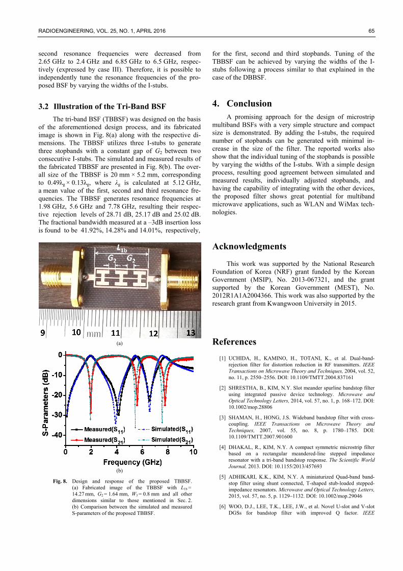
3.2 Illustration of the Tri-Band BSF
The tri-band BSF (TBBSF) was designed on the basis of the aforementioned design process, and its fabricated image is shown in Fig. 8(a) along with the respective di-mensions. The TBBSF utilizes three I-stubs to generate three stopbands with a constant gap of G2 between two consecutive I-stubs. The simulated and measured results of the fabricated TBBSF are presented in Fig. 8(b). The over-all size of the TBBSF is 20 mm × 5.2 mm, corresponding to 0.49λg × 0.13λg, where λg is calculated at 5.12 GHz, a mean value of the first, second and third resonance fre-quencies. The TBBSF generates resonance frequencies at 1.98 GHz, 5.6 GHz and 7.78 GHz, resulting their respec-tive rejection levels of 28.71 dB, 25.17 dB and 25.02 dB. The fractional bandwidth measured at a –3dB insertion loss is found to be 41.92%, 14.28% and 14.01%, respectively,
(a)
(b)
Fig. 8. Design and response of the proposed TBBSF. (a) Fabricated image of the TBBSF with L1b =
14.27 mm, G2 = 1.64 mm, W3 = 0.8 mm and all other dimensions similar to those mentioned in Sec. 2. (b) Comparison between the simulated and measured S-parameters of the proposed TBBSF.
for the first, second and third stopbands. Tuning of the TBBSF can be achieved by varying the widths of the I-stubs following a process similar to that explained in the case of the DBBSF.
4. Conclusion A promising approach for the design of microstrip
multiband BSFs with a very simple structure and compact size is demonstrated. By adding the I-stubs, the required number of stopbands can be generated with minimal in-crease in the size of the filter. The reported works also show that the individual tuning of the stopbands is possible by varying the widths of the I-stubs. With a simple design process, resulting good agreement between simulated and measured results, individually adjusted stopbands, and having the capability of integrating with the other devices, the proposed filter shows great potential for multiband microwave applications, such as WLAN and WiMax tech-nologies.
Acknowledgments
This work was supported by the National Research Foundation of Korea (NRF) grant funded by the Korean Government (MSIP), No. 2013-067321, and the grant supported by the Korean Government (MEST), No. 2012R1A1A2004366. This work was also supported by the research grant from Kwangwoon University in 2015.
References
[1] UCHIDA, H., KAMINO, H., TOTANI, K., et al. Dual-band-rejection filter for distortion reduction in RF transmitters. IEEE Transactions on Microwave Theory and Techniques, 2004, vol. 52, no. 11, p. 2550–2556. DOI: 10.1109/TMTT.2004.837161
[2] SHRESTHA, B., KIM, N.Y. Slot meander spurline bandstop filter using integrated passive device technology. Microwave and Optical Technology Letters, 2014, vol. 57, no. 1, p. 168–172. DOI: 10.1002/mop.28806
[3] SHAMAN, H., HONG, J.S. Wideband bandstop filter with cross-coupling. IEEE Transactions on Microwave Theory and Techniques, 2007, vol. 55, no. 8, p. 1780–1785. DOI: 10.1109/TMTT.2007.901600
[4] DHAKAL, R., KIM, N.Y. A compact symmetric microstrip filter based on a rectangular meandered-line stepped impedance resonator with a tri-band bandstop response. The Scientific World Journal, 2013. DOI: 10.1155/2013/457693
[5] ADHIKARI, K.K., KIM, N.Y. A miniaturized Quad-band band-stop filter using shunt connected, T-shaped stub-loaded stepped-impedance resonators. Microwave and Optical Technology Letters, 2015, vol. 57, no. 5, p. 1129–1132. DOI: 10.1002/mop.29046
[6] WOO, D.J., LEE, T.K., LEE, J.W., et al. Novel U-slot and V-slot DGSs for bandstop filter with improved Q factor. IEEE

66 G. R. KOIRALA, N. Y. KIM, MULTIBAND BANDSTOP FILTER USING AN I-STUB-LOADED MDMS
Transactions on Microwave Theory and Techniques, 2006, vol. 54, no. 6, p. 2840–2847. DOI: 10.1109/TMTT.2006.875450
[7] CHEN, F.C., ZHANG, N.Y., ZHANG, P.S., et al. Design of ultra-wideband bandstop filter using defected ground structure. Electronics Letters, 2013, vol. 49, no. 16, p. 1010–1011. DOI: 10.1049/el.2013.1541
[8] BARAL, R.N., SINGHAL, P.K. Recent techniques in design and implementation of microwave planar filters. Radioengineering, 2008, vol. 17, no. 4, p. 65–73.
[9] WANG, J., NING, H., XIONG, Q., et al. A novel miniaturized dual-band bandstop filter using dual-plane defected microstrip structures. Progress in Electromagnetics Research., 2013, vol. 134, p. 397–417.
[10] LA, D.S., HAN, W.H., ZHANG, J.L. Compact band-stop filters using π-shape DGS and π-shape DMS. Microwave and Optical Technology Letters, 2014, vol. 56, no. 11, p. 2504–2507. DOI: 10.1002/mop.28625
[11] XIAO, J.K., ZHU, Y.F., LI, Y. Controllable miniature tri-band bandpass filter using defected microstrip structure. Electronics Letters, 2013, vol. 50, no. 21, p. 1534–1536. DOI: 10.1049/el.2014.1432
[12] XIANG, Q.Y., FENG, Q.Y., HUANG, X.G. Bandstop filter based on complementary split ring resonators defected microstrip structure. Journal of Electromagnetic Waves and Applications, 2011, vol. 25, p. 1895–1908. DOI: 10.1163/156939311797453999
[13] XIAO, J. K., ZHU, Y. F. Multi-band bandstop filter using inner T-shaped defected microstrip structure (DMS). AEU-International Journal of Electronics and Communications, 2014, vol. 68, no. 2, p. 90–96. DOI: 10.1016/j.aeue.2013.07.002
[14] HONG, J.S., LANCASTER, M.J. Microstrip Filters for RF/Microwave Applications. 1st ed., New York: Wiley, 2001. ISBN: 0-471-22161-9
[15] ZHANG, H., CHEN, K.J. A tri-section stepped-impedance resonator for cross-coupled bandpass filters. IEEE Microwave and Wireless Components Letters, 2005, vol. 15, no. 6, p. 401–403. DOI: 10.1109/LMWC.2005.850475
[16] WANG, J., NING, H., XIONG, Q., et al. A compact narrow-band bandstop filter using spiral-shaped defected microstrip structure. Radioengineering, 2014, vol. 23, no. 1, p. 209–213.
About the Authors ... Gyan Raj KOIRALA was born in Nepal in 1987. He received the Bachelor of Engineering degree in Electronics and Communication Engineering in 2010 from Tribhuvan University, Nepal. Following his Bachelor’s Degree, Mr. Koirala served as a lecturer in Kathmandu Engineering College, Tribhuvan University, Nepal before joining Inte-grated M. S and Ph.D. Degree in Kwangwoon University, Seoul, Korea in 2014. His current research includes the design of RF/microwave devices, integrated passive device technology and RF biosensors.
Nam-Young KIM is the corresponding author for this manuscript. He was born in Korea in 1960. He has re-ceived two Masters and two Ph.D. degrees from State Uni-versity of New York at Buffalo and Midwest University: the M.S. and the Ph.D. in Electronic Engineering. The other degree is M.Div and D.C.E in Theology. He was a research scientist for CEEM at SUNY at Buffalo in 1994. After completing his research at CEEM at SUNY at Buf-falo, he joined the Department of Electronic Engineering of Kwangwoon University as an assistant professor in 1994. His main research focus is RFIC devices, ICs and systems that use wireless application techniques in order to develop high-speed structures in GaAs, Si, and other materials. The founder of the RFIC Center, Dr. Kim also serves as direc-tor for the Fusion Technology Center of RF and Bio-re-lated research. His RFIC research center was honored and sponsored as an ITRC (Information Technology Research Center) by the Ministry of Communication and Infor-mation (MIC) of Korea, where he has been acting Director of the RFIC since 2000. During his career, he has pub-lished 25 books, 171 refereed SCI journal papers and 304 refereed conference papers. Dr. Kim has been issued more than 60 patents and 96 semiconductor design patents. His research fields are the areas of RF semiconductor devices, RFICs and MMICs, LEDs and Biosensor applications.