multiple chemistry battery charger solution using the - microchip
TRANSCRIPT
AN1293Multiple Chemistry Battery Charger Solution Using the
MCP1631HV PIC® Device Attach PWM Controller
INTRODUCTIONThe history of modern day batteries began over twocenturies ago when Alessandro Volta invented the firstvoltaic pile. Since then the batteries have become acommon power source for industrial and consumerapplications. We usually find them in portable mediadevices. Some of these batteries are rechargeable andrequire modern and intelligent electronic circuits fortheir charge and discharge management. Managingthe batteries results in better energy efficiency andlonger life.
Battery charger designs have advanced quickly overthe last decade. New battery types with differentchemistries have been created. These new chemistriesrequired special charging profiles that were notavailable with conventional battery chargers. Previouscomplex power-management systems were developedusing high-speed analog pulse-width modulation(PWM) circuits combined with digital logic and specialtyanalog-only circuits. They were application specificoff-the-shelf solutions available for most applications.They had neither the features nor the flexibility to meetspecialized requirements. Modern power-managementapplications have advanced from simple current andvoltage regulators towards mixed signal applicationsutilizing programmable microcontrollers. Thecombination of a programmable microcontroller andhigh-speed PWM allows a designer the benefits ofprogrammability and customization. Themicrocontroller can adjust the output current, voltage,switching frequency, duty cycle, soft start, and handlesystem faults when external conditions warrant achange. Programmable battery chargers have theability to charge different battery pack chemistrieswithout changing any of the circuit hardware. Firmwareis used to handle the differences between the batterychemistries and their respective charge profiles.
This document will cover the recharging of Nickel MetalHydride (NiMH), Nickel Cadmium (NiCd) and LithiumIon (Li-Ion) batteries. It will also cover therecommended charge profiles for the NiMH/NiCd andLi-Ion battery chemistries.
The design example used in this application note is aDC-DC converter using the single-ended primaryinductive converter (SEPIC) topology. The low-costSEPIC design will concentrate on the use ofMicrochip’s MCP1631HV high-speed PWM device andthe PIC16F616 8-bit microcontroller. The firmwaresource code for this application note is available todownload from the Microchip web site. The firmware isfor the “MCP1631HV Digitally ControlledProgrammable Current Source Reference Design”evaluation board. The firmware is programmed inC language using the MikroElectronica mikroCcompiler for PIC® microcontrollers.
Charge Algorithms for Different ChemistriesThis section covers several battery chemistry chargeprofiles. When a designer starts to develop a batteryapplication, the first question regarding the batterymanagement is: “What is the appropriate chargealgorithm for this battery?” Different chemistries havedifferent charge profiles, and different manufacturershave different recommendations when it comes torestoring energy. This application note covers theNickel Metal Hydride (NiMH), Nickel Cadmium (NiCd),and Lithium Ion (Li-Ion) algorithms.
Author: Valentin C. Constantin Microchip Technology Inc.
2010 Microchip Technology Inc. DS01293B-page 1

AN1293
RECOMMENDED NiCd/NiMH CHARGE PROFILENiCd/NiMH cells may be rapid charged at a 1C ratewhen the cell voltage is between 0.9V and 1.8V. Theymay be rapid charged at room temperature with amaximum current of 1C, where 1C is the capacity ratingof the battery. The rapid charge rate may be between0.5C and 1C. Charging batteries at more than 1C willcause the internal battery temperature and pressure toincrease beyond manufacturing limits, resulting in thefailure of the battery. When the battery voltage is below0.9V, a preconditioning charge should be applied. Thepreconditioning charge rate is typically 0.2C in order toavoid a large temperature rise. A complete NiCd/NiMHcurrent charge profile with battery voltage andtemperature is illustrated in Figure 1..FIGURE 1: Typical NiMH and NiCd Charge Profile.Charge termination for NiMH batteries typically usesvoltage and temperature feedback. Two indications fordetermining when the battery has reached full chargeare a rapid increase in temperature (dT/dt), and a smalldrop in battery voltage (-dV/dt). The -dV/dt can bedifficult to detect for the NiMH batteries since thechange is very small. Lower charge rates result in asmaller -dV/dt change. If an Analog-to-DigitalConverter (ADC) is used for detection, the A/D con-verter must have enough bits of resolution to detect thesmall voltage change. The +dT/dt temperature rise istypically easier to detect. The NiMH cells should havean NTC thermistor attached for temperaturemonitoring. Both the -dV/dt and +dT/dt methods shouldbe used for a safe and robust design.
When the cell voltage drops 5 mV to 10 mV per cellduring rapid charge, the system should switch to thecharge Top Off mode. Rapid charge in ConstantCurrent mode should also be terminated if the batteryvoltage exceeds 1.8V per cell, or if the temperaturerises 1°C to 2°C within a 60 second interval. Top Offmode follows the Rapid Charge mode. Top Off mode isusually a one hour timed mode with the chargingcurrent set to a 0.05C rate. The total charge time for thebattery should be limited to the one hour Top Off timeplus the expected battery capacity divided by thecharge rate. Fifteen minutes or a similar amount of timemay be added to handle any pre-conditioning or otherdiscrepancies that may come up during charging.Limiting the total charge time is necessary in case thecells fail to charge properly.
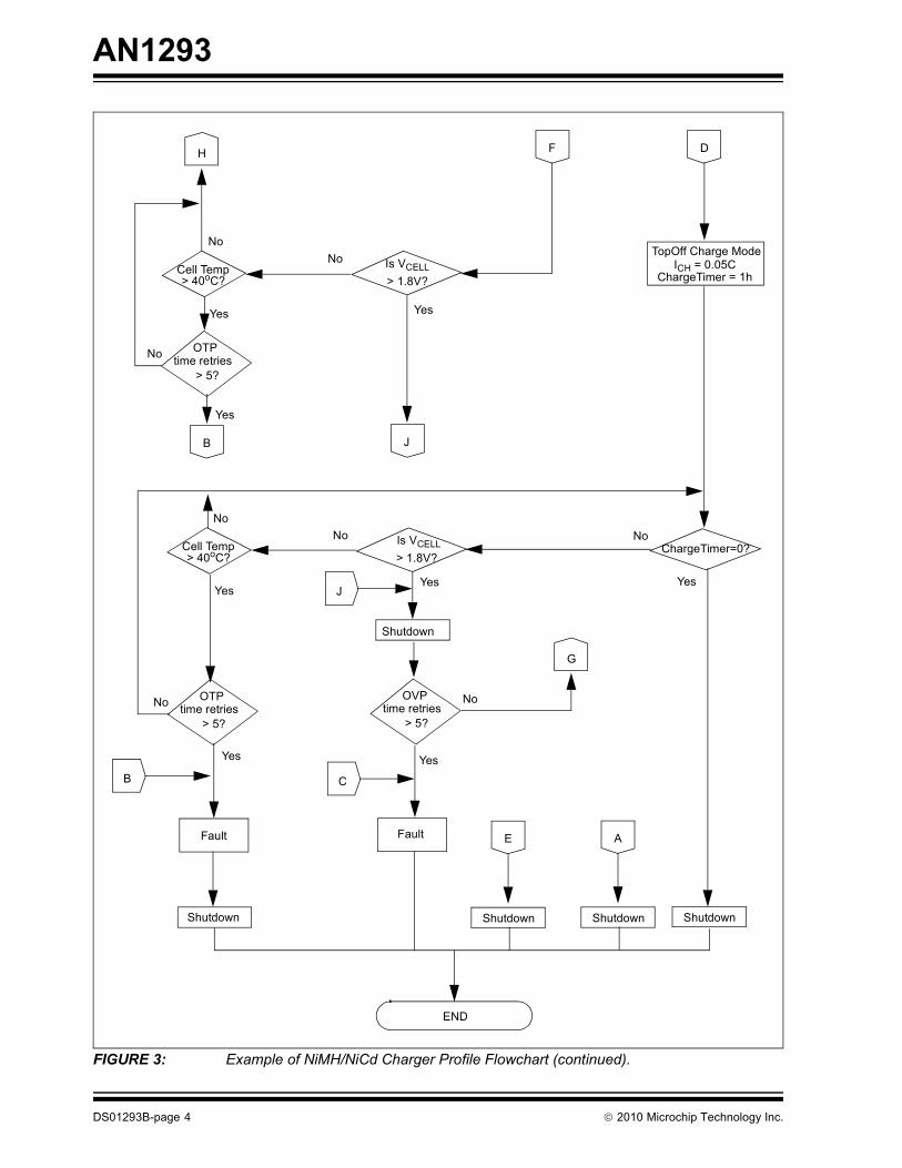
A summary flowchart that may be used as a startingreference for developing the firmware used to chargeNiMH and NiCd cells is illustrated in Figures 2 and 3.This flowchart follows the charge profile presented inFigure 1. The program starts with the microcontrollerinitialization. All charging parameters (cell C rate, fastcharging current, condition charge current, top offcharge current, number of cells, etc.) are loaded duringinitialization. A safety timer (ChargeTimer) is used toprevent overcharging if the normal cell chargetermination is not detected. The value of the chargetimer may be up to 4 or 5 hours, depending on the cellcapacity. A 1.8V overvoltage protection (OVP) per cellcheck will finish the charging if a cell is overcharged.The OVP condition is verified 5 times before shuttingdown the system. The cell overtemperature protection(OTP) will also be checked. The charge timer will bereloaded with 1 hour when entering Top Off mode.
DS01293B-page 2 2010 Microchip Technology Inc.

AN1293
FIGURE 2: Example of NiMH/NiCd Charger Profile Flowchart.
START
Is VCELL
Parameters, Timers;
No
Yes
Fast Charge Mode
dV/dt<-10mVdT/dt>1.5°C
Yes
> 0.9V? Pre-Charge
ICH=0.2C
Yes
No
Initialize: Processor,
SampleADC()
Start
No
Yes
ChargeTimer=0?Yes
No
No
Shutdown
OVPtime retries
> 5
Yes
No
Is VCELL> 1.8V?
Celltemp > 40°C?
No
OTPtime retries
> 5?
Yes
NoYes
Charging?
A
D
B
C
ChargeTimer=0?
Yes
EF HG
ICH = 1.0C
2010 Microchip Technology Inc. DS01293B-page 3
AN1293
FIGURE 3: Example of NiMH/NiCd Charger Profile Flowchart (continued).
TopOff Charge Mode
ChargeTimer = 1h
END
Shutdown
ChargeTimer=0?No
Yes
Cell Temp> 40oC?
Yes
No
OTPtime retries
> 5?
No
No
Yes
Shutdown
OVPtime retries
> 5?
Yes
No
Is VCELL > 1.8V?
ICH = 0.05C
Fault
Yes
Fault
G
Shutdown
CB
D
Cell Temp> 40oC?
Yes
NoNo
Yes
Is VCELL > 1.8V?
OTPtime retries
> 5?
No
Yes
B
H F
Shutdown
E
Shutdown
A
J
J
DS01293B-page 4 2010 Microchip Technology Inc.
AN1293
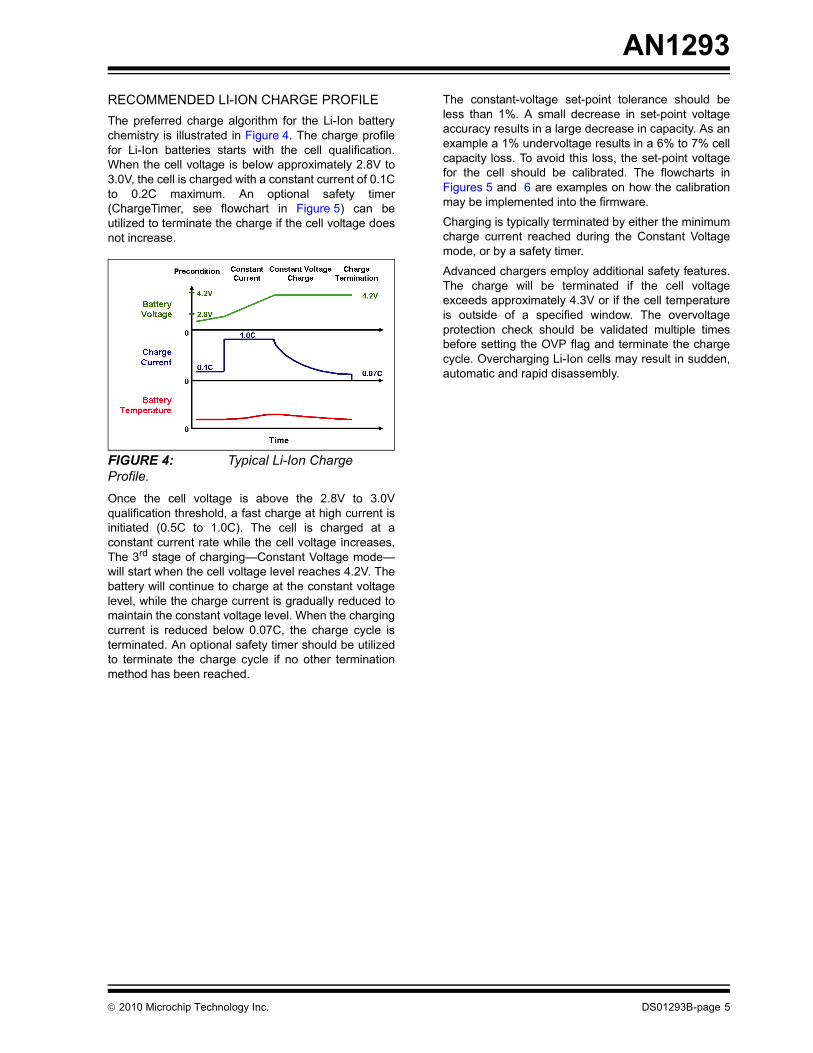
RECOMMENDED LI-ION CHARGE PROFILE The preferred charge algorithm for the Li-Ion batterychemistry is illustrated in Figure 4. The charge profilefor Li-Ion batteries starts with the cell qualification.When the cell voltage is below approximately 2.8V to3.0V, the cell is charged with a constant current of 0.1Cto 0.2C maximum. An optional safety timer(ChargeTimer, see flowchart in Figure 5) can beutilized to terminate the charge if the cell voltage doesnot increase.FIGURE 4: Typical Li-Ion Charge Profile.Once the cell voltage is above the 2.8V to 3.0Vqualification threshold, a fast charge at high current isinitiated (0.5C to 1.0C). The cell is charged at aconstant current rate while the cell voltage increases.The 3rd stage of charging—Constant Voltage mode—will start when the cell voltage level reaches 4.2V. Thebattery will continue to charge at the constant voltagelevel, while the charge current is gradually reduced tomaintain the constant voltage level. When the chargingcurrent is reduced below 0.07C, the charge cycle isterminated. An optional safety timer should be utilizedto terminate the charge cycle if no other terminationmethod has been reached.
The constant-voltage set-point tolerance should beless than 1%. A small decrease in set-point voltageaccuracy results in a large decrease in capacity. As anexample a 1% undervoltage results in a 6% to 7% cellcapacity loss. To avoid this loss, the set-point voltagefor the cell should be calibrated. The flowcharts inFigures 5 and 6 are examples on how the calibrationmay be implemented into the firmware.
Charging is typically terminated by either the minimumcharge current reached during the Constant Voltagemode, or by a safety timer.
Advanced chargers employ additional safety features.The charge will be terminated if the cell voltageexceeds approximately 4.3V or if the cell temperatureis outside of a specified window. The overvoltageprotection check should be validated multiple timesbefore setting the OVP flag and terminate the chargecycle. Overcharging Li-Ion cells may result in sudden,automatic and rapid disassembly.
2010 Microchip Technology Inc. DS01293B-page 5

AN1293
FIGURE 5: Example of Li-Ion Charger Profile Flowchart.
Initialize: Processor,
VCELL
Yes
No
VCELL> 3.0V?
Parameters, Timers; SampleADC()
CalibrateLiIon()Yes
No
Calibration?
VCELL<4.2V?Yes
ConstantCurrent Mode
Yes
NoPre-ChargeCurrent Mode ICH=0.2C
No
START
Request
OVP Test
Switch forYes
No
ChargeTimer=0?
Yes
start?
> 4.4V?
ICH = 1.0C
DecrementChargeTimer
No
Constant VoltageMode
BA C E
DS01293B-page 6 2010 Microchip Technology Inc.

AN1293
FIGURE 6: Example of Li-Ion Charger Profile Flowchart (continued).
END
ICH<= 0.07C?
Yes
No
Fault
Shutdown(charge complete) Shutdown
OVPtime retries
> 5?
Yes
No
VCELL>=4.2V?
Decrement IBATT
Shutdown
Charge Timer=0?
Yes
No
Yes
NoVCELL
OVP Test
> 4.4V?
D
Yes
DecrementChargeTimer
D
No
B C E
2010 Microchip Technology Inc. DS01293B-page 7

AN1293
SEPIC POWERTRAIN TOPOLOGYThe single-ended primary inductive converter (SEPIC)topology is similar to a flyback design with the additionof a coupling capacitor between the two inductors. Theoutput voltage may be less or greater than the inputvoltage.
This topology may use two inductors or a transformerwith coupled windings. A capacitor connected betweenthe windings offers DC isolation and protection againsta shorted load. The capacitor clamps the windingleakage inductance energy, removing the need for asnubber circuit. The inductive input smooths the inputcurrent and reduces the necessary filtering. The loadcurrent may be sensed using a ground referencedsense resistor connected to the secondary winding.
The SEPIC converter is ideal for battery chargersbecause of the inherent DC isolation and the reversevoltage blocking rectifier at the output.
A typical SEPIC converter topology is shown inFigure 7.
FIGURE 7: Single-Ended Primary Inductive Converter (SEPIC) Powertrain.
D
G
S
COUT
Rectifier DiodeCoupled Inductor
D
Solid State Switch
VOUTOutput
VIN
CIN
VEXT (PWM drive switch)
CS (current sense)
Rlimit Rload_sense
Iload_sense
CcCapacitative Isolation
DS01293B-page 8 2010 Microchip Technology Inc.

AN1293
The waveforms in Figure 8 are used to show how anSEPIC works.L1 and L2 are equal in inductance and are wound onthe same core. The NMOS switch (Q1) is turned on atthe start of a cycle. The L1 inductor current (IL1) startsramping up at a rate of VIN/L1.
FIGURE 8: SEPIC Converter Waveforms.The DC voltage across coupling capacitor VCc is equalto VIN. The current in the secondary winding (L2) willramp with VCc/L2 or VIN/L2. The NMOS switch currentis equal to the sum of the inductor currents IL1 and IL2during the switch-on time.
When Q1 turns off, the path for current flow will change.With Q1 off the path for current is now from the input,through L1 and the coupling capacitor (Cc) to theoutput. Another path for the current flow exists throughthe secondary winding (L2) to the output. During theswitch-off time the sum of L1 and L2 currents flow to theoutput through the rectifier. The current supplies theload and also replenishes the output capacitor (COUT).
Basic definitions for design are:
• TSW = Switching Period• fSW = Switching Frequency• tON = Switch-On Time• tOFF = Switch-Off Time• Duty Cycle, D = tON/TSW
The transfer function of the SEPIC converter inContinuous Current mode is:
EQUATION 1:
If the battery charging application has a low outputvoltage, the voltage drop (VD) across the outputrectifier diode should be considered. The voltage dropacross a Schottky diode is about 0.3V to 0.5V. Themaximum duty cycle (Dmax) for an application will be:
EQUATION 2:
D
G
SD
G
S
VOUT VIND
1 D–------------- =
Dmax VOUT VD+ VINmin VOUT VD+ + =
2010 Microchip Technology Inc. DS01293B-page 9

AN1293
The first step in calculating the inductor winding currentis to determine the maximum output power. Anefficiency estimate of 85% for the SEPIC topology maybe used to approximate the input current. The averageinput current is equal to the input power divided by theinput voltage.EQUATION 3:
EQUATION 4:
EQUATION 5:
When using a coupled inductor, the actual inductor willbe half the value of L in Equation 6 due to the mutualcoupling. The inductor value for the coupled windingsis calculated by:
EQUATION 6:
where IL is the selected peak-to-peak ripple outputcurrent. A good IL selection is 20% of the outputcurrent.
Once the winding inductance (L) and duty cycle (D) areresolved, calculate the maximum inductor ripple andpeak currents for L1 and L2 that will prevent saturatingthe inductors.
EQUATION 7:
EQUATION 8:
Using VCc = VIN yields:
EQUATION 9:
The coupled inductor winding currents calculatedbelow are used to determine the size of the inductornecessary.
EQUATION 10:
EQUATION 11:
The switch current (IQ1) is equal to the combination ofthe winding currents during the switch-on time: IL1+IL2.The peak Q1 switch voltage is equal toVINmax + VOUTmax.
The cathode of the SEPIC Schottky diode is connectedto VOUT and the anode of the schottky diode isconnected to the SEPIC coupling capacitor. Thevoltage across the coupling capacitor is equal to VIN.When Q1 is on, the voltage across the SEPIC diode is:
EQUATION 12:
To estimate the coupling capacitor capacitance, thecapacitor derivative equation can be used:
EQUATION 13:
For the SEPIC converter coupling capacitor, thevoltage is approximated to be a DC value whenderiving the duty cycle. The SEPIC capacitor must berated for the RMS current. As output power increases,the capacitor ripple current will increase as well. Thismakes the SEPIC converter better for lower powerapplications where the RMS current through thecapacitor is relatively small. The maximum RMScurrent in the coupling capacitor will occur at maximumoutput power and minimum input voltage.
EQUATION 14:
The ripple voltage (VCc) should be no more than 5%of the voltage across the capacitor.
POUT VOUT IOUT=
PIN POUT Efficiency =
IIN AVG PIN VIN=
L2--- VINmin Dmax 2 IL fSW =
IL1ON VIN tON L=
IL2ON VCc tON L=
IL2ON VIN tON L=
IL1peak IIN AVG 12---
IL1ON+=
IL2peak IOUT AVG 12--- IL2ON+=
VD VOUT VIN VOUT VCc+ =+=
CC ICctV-------=
CcIOUT
VCc------------- Dmax
fSW------------- =
DS01293B-page 10 2010 Microchip Technology Inc.

AN1293
The same equation should be applied to the outputcapacitor. The output current is supplied by the outputcapacitor COUT during the switch ON time.EQUATION 15:
The input capacitor CIN should be capable of handlingthe input RMS current. The input current waveform iscontinuous and triangular. The inductive input ensuresthat the input capacitor sees low ripple currents fromthe power supply. The input capacitor provides a low-impedance source for the SEPIC converter in caseswhere the power source is not immediately adjacent tothe SEPIC powertrain.
MCP1631HV AND SEPIC CONVERTER IN A MULTI-CHEMISTRY CHARGER APPLICATION
DESIGN EXAMPLE
MCP1631HV PWM ControllerThe MCP1631HV integrates the necessary blocks todevelop an intelligent programmable battery charger. Itprovides a regulated bias voltage for internal circuitryand external devices. It is available with two regulatedoutput voltage options, +5.0V and +3.3V. The on-boardregulator can supply a maximum output current of250 mA. The maximum input voltage range for theregulator is +16.0V.
The MCP1631HV has an oscillator input pin (OSC_IN)that may be supplied by a microcontroller PWM outputor by a simple clock output (50% duty cycle). When theoscillator input is high, the VEXT output pin is pulled low(Figure 9).
When OSC_IN input transitions from a high to a lowlevel, the internal N-channel MOSFET driver will turnoff and the P-channel MOSFET will turn on, driving theVEXT pin high. The VEXT pin connects to the gate of anexternal N-channel MOSFET. The MOSFET will turn onwhen the VEXT pin goes high. Current begins to rampup in the external CS sense resistor until it reaches onethird of the level of the error amplifier output voltage,which is limited to 0.9V by an error amplifier clamp. The0.9V limit is used as an overcurrent limit. A filter is usedon the CS input to remove the spikes associated withthe turn on of the external power MOSFET. TheMCP1631HV P-channel driver MOSFET is poweredusing a separate PVDD pin to keep switching noise offon AVDD pin and sensitive CS circuitry.
Any difference between the VREF and VFB inputs of theA1 error amplifier are quickly removed. If the VFB inputis high, the inverting error amplifier output (COMP) willbe pulled down. The peak current into the switch will belowered, and the duty cycle will be shortened in orderto bring the output back into regulation. The external Rand C used for compensation are used to control thespeed of the error amplifier output response. If notcompensated properly, the error amplifier output maybe underdamped (oscillations) or overdamped (slowresponse). The VREF input may be set by amicrocontroller to program the proper charge current.
The SEPIC topology does not require a current senseresistor to be connected directly to the battery becausethe current into secondary winding is equal to thecurrent flowing into the battery. A sense resistor will beused to sense the secondary current. TheMCP1631HV integrates a 10 V/V gain inverting ampli-fier for buffering the battery current sense signal.
The battery voltage is sensed using the A/D converterof the PIC16F616 microcontroller. The MCP1631HVdevice integrates a low-current amplifier (A3),configured as a unity gain buffer. The amplifier is usedto buffer the battery voltage sense signal, allowing theuse of high value resistors in the battery voltage feed-back divider network.
Overvoltage (OV) protection is required for any currentsource application. The MCP1631HV device integratesan internal high-speed OV comparator which has a1.2V reference. If the voltage on the OV_IN pinexceeds the 1.2V threshold, the VEXT output is asyn-chronously terminated. Switching will resume after thevoltage has dropped by more than hysteresis value of50 mV. If a battery is removed during the charge cycle,the charger output voltage will be limited to a safe valueby the OVP circuitry.
COUTIOUTV OUT----------------- D
fSW-------- =
2010 Microchip Technology Inc. DS01293B-page 11

AN1293
FIGURE 9: MCP1631HV PWM Controller – Functional Block Diagram.
MCP1631HV High-Speed PIC® Device PWM
R
S Q
Q
A1+
-VREF
FB
C1+
-
CS/VRAMP
OSCIN
PVDD
COMP
PGND
VEXT
2R
2.7V Clamp
OT
UVLO
100 kΩ
0.1 µA
VDD
R
+
- R
R
10R
+
-
A2
A3
+3.3V or +5.0V LDO 250 mA
VIN
AVDD_OUT / AVDD_IN
VDD
Shutdown ControlA3 Remains OnSHDN
ISIN
ISOUT
VSIN
VSOUT
C2+
-
VDD
AGND
OVIN
Overvoltage Compwith Hysteresis
Internal1.2V VREF
OSCDIS
100 kΩ
Internal Regulator for MCP1631HV
VDD
VDD
VDD
VDD
VDD
Note 1: On shutdown, amplifier A3 remains functional so the batteryvoltage can be sensed during discharge phase.
DS01293B-page 12 2010 Microchip Technology Inc.
AN1293
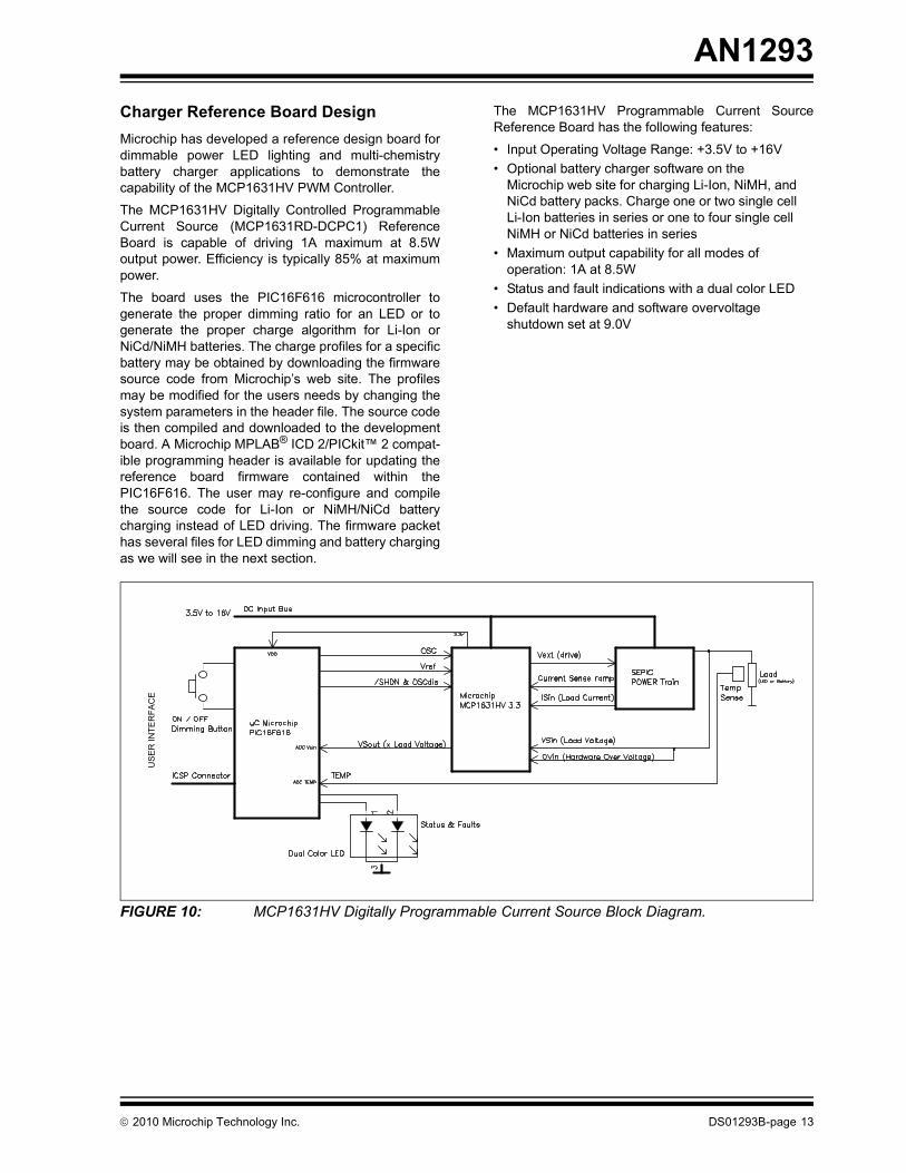
Charger Reference Board DesignMicrochip has developed a reference design board fordimmable power LED lighting and multi-chemistrybattery charger applications to demonstrate thecapability of the MCP1631HV PWM Controller.The MCP1631HV Digitally Controlled ProgrammableCurrent Source (MCP1631RD-DCPC1) ReferenceBoard is capable of driving 1A maximum at 8.5Woutput power. Efficiency is typically 85% at maximumpower.
The board uses the PIC16F616 microcontroller togenerate the proper dimming ratio for an LED or togenerate the proper charge algorithm for Li-Ion orNiCd/NiMH batteries. The charge profiles for a specificbattery may be obtained by downloading the firmwaresource code from Microchip’s web site. The profilesmay be modified for the users needs by changing thesystem parameters in the header file. The source codeis then compiled and downloaded to the developmentboard. A Microchip MPLAB® ICD 2/PICkit™ 2 compat-ible programming header is available for updating thereference board firmware contained within thePIC16F616. The user may re-configure and compilethe source code for Li-Ion or NiMH/NiCd batterycharging instead of LED driving. The firmware packethas several files for LED dimming and battery chargingas we will see in the next section.
The MCP1631HV Programmable Current SourceReference Board has the following features:
• Input Operating Voltage Range: +3.5V to +16V• Optional battery charger software on the
Microchip web site for charging Li-Ion, NiMH, and NiCd battery packs. Charge one or two single cell Li-Ion batteries in series or one to four single cell NiMH or NiCd batteries in series
• Maximum output capability for all modes of operation: 1A at 8.5W
• Status and fault indications with a dual color LED• Default hardware and software overvoltage
shutdown set at 9.0V
FIGURE 10: MCP1631HV Digitally Programmable Current Source Block Diagram.
US
ER
INTE
RFA
CE
2010 Microchip Technology Inc. DS01293B-page 13

AN1293
The MCP1631HV Digitally Programmable CurrentSource Reference Design has a red/green dual colorLED (D2) to indicate status and faults. The green LEDwill flash for one second when the system is activatedand current is being supplied to the load.The push button (S1 in Figure 11) is used to enable theoutput and start the charge algorithm according to theflowcharts presented in Figures 2, 3, 5 and 6. PressingS1 again will turn off the output current. If a Faultcondition such as no load, overvoltage, orovertemperature is present when attempting to turn theoutput on, the system will stay off and the Faultcondition will be indicated by the flashing red indicatorLED. The faults are coded as follows:
• Thermal Shutdown – Red LED flashes at 1 Hz rate if an overtemperature of the LED case has been detected
• Overvoltage Shutdown – Red LED flashes at 2 Hz rate if an overvoltage or a missing/open load has been detected
An overvoltage/overtemperature Fault condition will beverified 5 times by the microcontroller firmware beforethe fault is validated and the system shuts down.
Two parallel resistors, R10 and R11, are used to sensethe MOSFET switch (Q1) current (Figure 11).The current sense signal is applied to the CScomparator input of MCP1631HV. The load current isequal to the current in the secondary inductor L1:B.Sense resistors R2 and R3 are used to sense the loadcurrent. The load sense signal is amplified by theISin current sense amplifier before entering the feed-back pin (FB). A reference voltage signal from thePIC16F616 supplies the VREF current referencevoltage for the MCP1631HV. The pulse-widthmodulated VEXT signal that drives the MOSFET switchis generated by the MCP1631HV device using themicrocontroller current reference PWM signal and theload current feedback signal. The current feedbacksignal is integrated with the current reference signal.The integrated signal is compared with the switchcurrent sense and an artificial compensation ramp tomodulate the switch drive signal. The artificialcompensation ramp is generated from the PIC16F616OSC output signal to prevent the system fromswitching between continuous and discontinuousoperation. The bi-modal operation would cause theduty cycle to vary when D>50%. The artificial rampvoltage supplements the switch current sense voltageto ensure the CS signal rises above the referencesignal before the end of the integrator period. TheMOSFET switch will be turned off when the CS signalrises above the reference signal and resets theintegrator. The artificial ramp slope for the SEPIC willbe the same as the slope of the current during the OFFtime of the oscillator. The artificial ramp circuit blockconsists of C10, R9, R13 and Q2, which is driven with theOSC signal.
A resistor divisor network composed of R5, R8 and R15is used for load voltage sensing. R5 sensesovervoltage conditions. R8 senses the load voltage.The load voltage tap at R8 is connected to theMCP1631HV internal voltage follower amplifier via theVSIN pin. The corresponding VSOUT signal is fed to thePIC16F616 A/D RA2 port.
When a thermistor is used, it is placed across J2-4 andJ2-5. The thermistor forms a voltage divider with R1, a10K resistor. The voltage across the thermistor is fed tothe A/D port RA4 of the PIC16F616. If anovertemperature condition is detected, themicrocontroller will disable the PWM signal ofMCP1631HV.
The OSC signal is generated directly by thePIC16F616 PWM hardware at port RC5.
DS01293B-page 14 2010 Microchip Technology Inc.

AN1293
FIGURE 11: MCP1631HV Programmable Current Source Reference Design Schematic.
M
3
1
2
5
8 3
4
67
12
2010 Microchip Technology Inc. DS01293B-page 15
AN1293
The firmware is compiled with the following outputcapabilities:• 1A output current for one Li-Ion cell or 500 mA for two series cells
• 700 mA for 1, 2 and 4 NiMH or NiCd cells
The charge profiles may be modified by editing andrecompiling the source code that can be downloadedfrom Microchip’s web site. The Gerber file for theMCP1631HV-DCPC1 Reference Board may also bedownloaded from the Microchip web site.
MCP1631RD-DCPC1 Programmable Current Source Reference Design FirmwareThe source code for Microchip’s MCP1631HV DigitallyControlled Programmable Current Source ReferenceDesign Board was developed using MikroElektronica’smikroC Compiler for PIC® Microcontrollers. Thesoftware has conditional compiler options for userselectable parameters and functions. The LED driver isthe default compiler option. The NiMH/NICd and Li-Ionbattery charger options are selectable at compile timeby modifying a parameter in the header file. ThemikroC compiler may be downloaded fromhttp://www.mikroe.com. Please consult the mikroCweb site and compiler Help for more information.
The firmware packet has the following hex files:
• LED = 00234R1.hex
• Li-Ion = 00234R1-LiIon_Charger.hex
• NiMH/NiCd = 00234R1-NiMH_NiCd_Charger.hex
The C source code file is 00234R1.c and the setupheader file is 00234R1.h. These two files are includedin the mikroC project file: 00234R1.ppc.
To modify the system profile, the user edits the00234R1.h file. Set the profile of interest for thereference board to “Enabled”. The example below is fora single 1000 mAh Li-Ion cell:/* Enable support for Lithium Ion batteries */
#define LION_SUPPORT EBNABLED
/* Enable support for Nickel Metal Hydride batteries*/
#define NIMH_SUPPORT DISABLED
/* Enable support for LED Driver */
#define LED_DRIVER_SUPPORT DISABLED
The charging current profile parameters are set inseparate sections of the header file for the project. Thecell overvoltage value is set to 200 mV by theparameter LI_ION_OVER_VOLTAGE_CHARGE. The0.2C Li-Ion condition current value is set to 200 mA bythe parameter LI_ION_CONDITION_CURRENT. Thecell conditioning voltage set point is set at 3.0V byLI_ION_CONDITION_VOLTAGE. The maximumbattery charge current in Constant Current mode is setto 1000 mA by the LI_ION_CHARGE_CURRENTparameter. The 0.07C charge termination point forConstant Voltage mode is defined as 70 mA byLI_ION_CHARGE_TERMINATION_CURRENT. Thedefault number of cells to charge is set to 1 byNUMBER_OF_CELLS_DEFAULT. The overtemperatureset point can be enabled or disabled by setting theOVERTEMPERATURE_SUPPORT parameter. The defaultovertemperature set point is +40oC. A 10K NTCtermistor inside the battery pack must be connectedbetween J2-4 and J2-5 of the J2 connector (see theschematic in Figure 11) when the overtemperaturefeature is enabled.#if (LION_SUPPORT == ENABLED)
//------------------------------------------------
// define the LiIon charge characteristics (in mil-livolts and milliamps) for 1000mAh Cells
//------------------------------------------------
/* cell overvoltage charge = (150 mV to 200 mV) */
#define LI_ION_OVER_VOLTAGE_CHARGE
((int) (200.0/BATTERY_MV_PER_BIT))
/* cell conditioning current = 200 mA (0.2C) */
#define LI_ION_CONDITION_CURRENT
((int)(200.0/BATTERY_MA_PER_BIT))
/* cell conditioning voltage = 3.0V */
#define LI_ION_CONDITION_VOLTAGE
((int)(3000.0/BATTERY_MV_PER_BIT))
/* total charge current = 1000 milliamps max */
#define LI_ION_CHARGE_CURRENT
((int)(1000.0/BATTERY_MA_PER_BIT))
/* charge termination current = 70 mA (0.07C) */
#define LI_ION_CHARGE_TERMINATION_CURRENT
((int)(70.0/BATTERY_MA_PER_BIT))
#define OVERTEMPERATURE_SUPPORT DISABLED
/* default number of cells */
#define NUMBER_OF_CELLS_DEFAULT 1
#endif /* LION_SUPPORT */
DS01293B-page 16 2010 Microchip Technology Inc.

AN1293
The OSC reference signal supplied to theMCP1631HV PWM controller is set by the PIC16F616.The frequency may be set to 200 kHz or 500 kHz. Theparameters are set in the main C file, 00234R1.c. TheOSC frequency is dependant upon the SEPICinductance and load. The default values should not bechanged for the reference board./* define Oscillator Output PWM frequency PrescaleValue for PR2 */#define OSC_500KHZ_PR2_REG 0x03
#define OSC_200KHZ_PR2_REG 0x09
#define OSC_PR2_REG OSC_500KHZ_PR2_REG
The oscillator duty cycle is set to 25% if the SEPICreference board must work in Buck-Boost mode. The25% duty cycle allows the system to boost the outputvoltage. The parameter is in the 00234R1.h headerfile./* charge oscillator duty cycle */
#define OSCILLATOR_DUTY_CYCLE 25
Design ExampleThis is an example design for two 500 mAh Li-Ion cellsconnected in series.
• Input Voltage, VIN=12V• Output Voltage range, VCELL from 0 to 8.4V• Fast charge current at 1.0C, ICH=500 mA• Switching frequency, fSW=500 kHz
We start from Equation 2 calculating the maximum dutycycle using 0.4V for the voltage drop of a Schottkydiode:
Given the switching frequency fsw = 500 kHz, tON is:
Calculate Maximum Output Power:
The typical efficiency of a SEPIC converter in thispower range, using a Schottky diode for the outputrectifier, is around 85%. According to Equation 4 theinput power is:
The average input current is equal to the input powerdivided by the input voltage (see Equation 5):
The inductor value for coupled windings results fromEquation 6. IL is the selected peak-to-peak outputripple current, which is 20% of the output current:
The inductance is calculated to be 50.4 µH. Select astandard inductor value of 47 µH. Choosing a lowervalue for the inductor will result in an increase of ripplecurrent by over 20%. Attention must be paid to theinductor, not to saturate.
A 47 µH inductor looks like a 94 µH inductor forcoupled inductors. Larger inductance reduces ripplecurrent.
Next, we calculate the ripple and peak inductorcurrents.
The input and output inductor ripple current is equal to(see Equations 7 and 8):
The peak input current is:
The peak output current (IOUT(AVG) = ICH):
Dmax 8.4V 0.4V+ 12V 8.4V 0.4V+ + =
Dmax 42%=
tON Dmax fSW=
tON 0.42 500kHz =
tON 840ns=
POUT VCELLmax ICH=
POUT 8.4V 500mA=
POUT 4.2W=
PIN 4.2W 0.85=PIN 4.94W=
IIN AVG 4.94W 12V =
IIN AVG 412mA=
IL = 500 mA x 0.2 = 100 mAL 2 12V 0.42 2 100mA 500kHz =L 2 50.4H=
IL1ON IL2ON=
IL1ON 12V 0.84 6–10 s 94 6–10 H =
IL1ON 108mA=
IL1peak IIN AVG 0.5 IL1ON+=
IL1peak 412mA 0.5 108mA+=
IL1peak 466mA=
IL2peak IOUT AVG 0.5 IL2ON+=
IL2peak 500mA 0.5 108mA+=
IL2peak 554mA=
2010 Microchip Technology Inc. DS01293B-page 17
AN1293
A Wurth® Elektronik WE-DD744878470 surface mountshielded power transformer is selected.The switch current of the NMOS transistor (IQ1) is equalto the combination of the winding currents during theswitch-on time:
The peak switch voltage on the transistor and Schottkydiode is equal to:
The peak NMOS switch current and peak switchvoltage help to choose the proper devices. AnN-channel MOSFET with 30VDS, 30 m, logic-levelswitch Si4346DY from Vishay Siliconix is selected. Theaverage current through the output Schottky diode isequal to the output current (ICH). A Schottky diode witha 30V or greater reverse-voltage rating is used.
The coupling capacitor is calculated using Equation 14:
A standard 1 µF X7R 25V rated ceramic capacitor canbe used. The coupling capacitor must also be able tohandle the current flowing during switch on (tON) andoff times (tOFF). Use the RMS expression of atrapezoidal waveform to determine the RMS current ofthe coupling capacitor:
where I1 is the lowest waveform current and I2 is thehighest waveform current: I1=IAVG+(Iripple/2) andI2=IAVG–(Iripple/2).
For Q1 turned on IAVG=IOUT(AVG) and Iripple=tON x2VIN/(4L). For this case I1 will be:
and I2 will be:
For Q1 turned off IAVG=-IIN(AVG) and Iripple=tOFFx2VIN/(4L). As shown above I1 and I2 in this stageof switching will be:
The worst-case SEPIC coupling capacitor current is:
Output capacitor selection:
A standard 1 µF X7R at 16V DC rating and low ESRceramic capacitor can be used. During L1 charging theoutput current is supplied by COUT.
IQ1peak IL1peak IL2peak+=
IQ1peak 1.02A=
VSW VIN VCELL+=
VSW 12V 8.4V+=
VSW 20.4V=
IOUT ICH 500mA==
V Cc 0.05 VIN 600mV==
Cc500mA600mV----------------- 0.42
500kHz------------------- =
Cc 0.7F=
ICcRMS D I12 I2
2 I1 I2 + + 3=
I1ON 0.5A 0.84 10 6– s 12V 94 10 6– H 2+=
I1ON 0.5A 0.054A 0.554A=+=
I2ON 0.5A 0.054A– 0.446A= =
ICcRMS ON 0.42 0.5542 0.4462 0.247 + + 3 =
ICcRMS ON 324mA=
I1OFF 0.412A– 1.16 10 6– s 12V 94 10 6– H 2+=
I1OFF 0.412A– 0.074A 0.338A–=+=
I2OFF 0.412A– 0.074A 0.486A–=–=
ICcRMS OFF 0.58 0.3382 0.4862 0.164 + + 3 =
ICcRMS OFF 315mA=
ICcRMS ICcRMS ON 2 ICcRMS OFF
2+ =
ICcRMS 0.3242 0.3152+ 453mA==
V OUT 0.05 VCELL 420mV==
COUT500mA420mV----------------- 0.42
500kHz------------------- =
COUT 1F=
DS01293B-page 18 2010 Microchip Technology Inc.
AN1293
CONCLUSIONFor applications that require intelligent powermanagement solutions like battery chargers, thecombination of a microcontroller and the MCP1631HVhigh-speed PWM is very powerful. It brings theprogrammable benefits of the microcontroller and addsthe performance of a high-speed analog PWM. Theanalog PWM will respond to changes in input voltageand output current very quickly. The microcontroller isused for programmability, for establishing chargecurrent, for monitoring the circuit for Fault conditions,and for taking the appropriate action in the event of aspecific fault.
References[1] AN1137, “Using the MCP1631 Family to
Develop Low-Cost Battery Chargers”, TerryCleveland, Microchip Technology Inc., ©2007
[2] AN960, “New Components and Design MethodsBring Intelligence to Battery Chargers”, TerryCleveland, Microchip Technology Inc., ©2004
[3] MCP1631/HV/MCP1631V/VHV Data Sheet,“High-Speed, Pulse–Width Modulator”,DS22063, Microchip Technology Inc., ©2008
[4] MCP1631HV Digitally ControlledProgrammable Current Source ReferenceDesign, DS51798, Microchip Technology Inc.,©2009
[5] “MCP1631HV Multi-Chemistry Battery ChargerReference Design”, DS51791A, MicrochipTechnology Inc., ©2009
2010 Microchip Technology Inc. DS01293B-page 19

AN1293
NOTES:DS01293B-page 20 2010 Microchip Technology Inc.
Note the following details of the code protection feature on Microchip devices:• Microchip products meet the specification contained in their particular Microchip Data Sheet.
• Microchip believes that its family of products is one of the most secure families of its kind on the market today, when used in the intended manner and under normal conditions.
• There are dishonest and possibly illegal methods used to breach the code protection feature. All of these methods, to our knowledge, require using the Microchip products in a manner outside the operating specifications contained in Microchip’s Data Sheets. Most likely, the person doing so is engaged in theft of intellectual property.
• Microchip is willing to work with the customer who is concerned about the integrity of their code.
• Neither Microchip nor any other semiconductor manufacturer can guarantee the security of their code. Code protection does not mean that we are guaranteeing the product as “unbreakable.”
Code protection is constantly evolving. We at Microchip are committed to continuously improving the code protection features of ourproducts. Attempts to break Microchip’s code protection feature may be a violation of the Digital Millennium Copyright Act. If such actsallow unauthorized access to your software or other copyrighted work, you may have a right to sue for relief under that Act.
Information contained in this publication regarding deviceapplications and the like is provided only for your convenienceand may be superseded by updates. It is your responsibility toensure that your application meets with your specifications.MICROCHIP MAKES NO REPRESENTATIONS ORWARRANTIES OF ANY KIND WHETHER EXPRESS ORIMPLIED, WRITTEN OR ORAL, STATUTORY OROTHERWISE, RELATED TO THE INFORMATION,INCLUDING BUT NOT LIMITED TO ITS CONDITION,QUALITY, PERFORMANCE, MERCHANTABILITY ORFITNESS FOR PURPOSE. Microchip disclaims all liabilityarising from this information and its use. Use of Microchipdevices in life support and/or safety applications is entirely atthe buyer’s risk, and the buyer agrees to defend, indemnify andhold harmless Microchip from any and all damages, claims,suits, or expenses resulting from such use. No licenses areconveyed, implicitly or otherwise, under any Microchipintellectual property rights.
2010 Microchip Technology Inc.
Trademarks
The Microchip name and logo, the Microchip logo, dsPIC, KEELOQ, KEELOQ logo, MPLAB, PIC, PICmicro, PICSTART, PIC32 logo, rfPIC and UNI/O are registered trademarks of Microchip Technology Incorporated in the U.S.A. and other countries.
FilterLab, Hampshire, HI-TECH C, Linear Active Thermistor, MXDEV, MXLAB, SEEVAL and The Embedded Control Solutions Company are registered trademarks of Microchip Technology Incorporated in the U.S.A.
Analog-for-the-Digital Age, Application Maestro, CodeGuard, dsPICDEM, dsPICDEM.net, dsPICworks, dsSPEAK, ECAN, ECONOMONITOR, FanSense, HI-TIDE, In-Circuit Serial Programming, ICSP, Mindi, MiWi, MPASM, MPLAB Certified logo, MPLIB, MPLINK, mTouch, Octopus, Omniscient Code Generation, PICC, PICC-18, PICDEM, PICDEM.net, PICkit, PICtail, REAL ICE, rfLAB, Select Mode, Total Endurance, TSHARC, UniWinDriver, WiperLock and ZENA are trademarks of Microchip Technology Incorporated in the U.S.A. and other countries.
SQTP is a service mark of Microchip Technology Incorporated in the U.S.A.
All other trademarks mentioned herein are property of their respective companies.
© 2010, Microchip Technology Incorporated, Printed in the U.S.A., All Rights Reserved.
Printed on recycled paper.
ISBN: 978-1-60932-159-8
DS01293B-page 21
Microchip received ISO/TS-16949:2002 certification for its worldwide headquarters, design and wafer fabrication facilities in Chandler and Tempe, Arizona; Gresham, Oregon and design centers in California and India. The Company’s quality system processes and procedures are for its PIC® MCUs and dsPIC® DSCs, KEELOQ® code hopping devices, Serial EEPROMs, microperipherals, nonvolatile memory and analog products. In addition, Microchip’s quality system for the design and manufacture of development systems is ISO 9001:2000 certified.

DS01293B-page 22 2010 Microchip Technology Inc.
AMERICASCorporate Office2355 West Chandler Blvd.Chandler, AZ 85224-6199Tel: 480-792-7200 Fax: 480-792-7277Technical Support: http://support.microchip.comWeb Address: www.microchip.comAtlantaDuluth, GA Tel: 678-957-9614 Fax: 678-957-1455BostonWestborough, MA Tel: 774-760-0087 Fax: 774-760-0088ChicagoItasca, IL Tel: 630-285-0071 Fax: 630-285-0075ClevelandIndependence, OH Tel: 216-447-0464 Fax: 216-447-0643DallasAddison, TX Tel: 972-818-7423 Fax: 972-818-2924DetroitFarmington Hills, MI Tel: 248-538-2250Fax: 248-538-2260KokomoKokomo, IN Tel: 765-864-8360Fax: 765-864-8387Los AngelesMission Viejo, CA Tel: 949-462-9523 Fax: 949-462-9608Santa ClaraSanta Clara, CA Tel: 408-961-6444Fax: 408-961-6445TorontoMississauga, Ontario, CanadaTel: 905-673-0699 Fax: 905-673-6509
ASIA/PACIFICAsia Pacific OfficeSuites 3707-14, 37th FloorTower 6, The GatewayHarbour City, KowloonHong KongTel: 852-2401-1200Fax: 852-2401-3431Australia - SydneyTel: 61-2-9868-6733Fax: 61-2-9868-6755China - BeijingTel: 86-10-8528-2100 Fax: 86-10-8528-2104China - ChengduTel: 86-28-8665-5511Fax: 86-28-8665-7889China - ChongqingTel: 86-23-8980-9588Fax: 86-23-8980-9500China - Hong Kong SARTel: 852-2401-1200 Fax: 852-2401-3431China - NanjingTel: 86-25-8473-2460Fax: 86-25-8473-2470China - QingdaoTel: 86-532-8502-7355Fax: 86-532-8502-7205China - ShanghaiTel: 86-21-5407-5533 Fax: 86-21-5407-5066China - ShenyangTel: 86-24-2334-2829Fax: 86-24-2334-2393China - ShenzhenTel: 86-755-8203-2660 Fax: 86-755-8203-1760China - WuhanTel: 86-27-5980-5300Fax: 86-27-5980-5118China - XianTel: 86-29-8833-7252Fax: 86-29-8833-7256China - XiamenTel: 86-592-2388138 Fax: 86-592-2388130China - ZhuhaiTel: 86-756-3210040 Fax: 86-756-3210049
ASIA/PACIFICIndia - BangaloreTel: 91-80-3090-4444 Fax: 91-80-3090-4123India - New DelhiTel: 91-11-4160-8631Fax: 91-11-4160-8632India - PuneTel: 91-20-2566-1512Fax: 91-20-2566-1513Japan - YokohamaTel: 81-45-471- 6166 Fax: 81-45-471-6122Korea - DaeguTel: 82-53-744-4301Fax: 82-53-744-4302Korea - SeoulTel: 82-2-554-7200Fax: 82-2-558-5932 or 82-2-558-5934Malaysia - Kuala LumpurTel: 60-3-6201-9857Fax: 60-3-6201-9859Malaysia - PenangTel: 60-4-227-8870Fax: 60-4-227-4068Philippines - ManilaTel: 63-2-634-9065Fax: 63-2-634-9069SingaporeTel: 65-6334-8870Fax: 65-6334-8850Taiwan - Hsin ChuTel: 886-3-6578-300Fax: 886-3-6578-370Taiwan - KaohsiungTel: 886-7-536-4818Fax: 886-7-536-4803Taiwan - TaipeiTel: 886-2-2500-6610 Fax: 886-2-2508-0102Thailand - BangkokTel: 66-2-694-1351Fax: 66-2-694-1350
EUROPEAustria - WelsTel: 43-7242-2244-39Fax: 43-7242-2244-393Denmark - CopenhagenTel: 45-4450-2828 Fax: 45-4485-2829France - ParisTel: 33-1-69-53-63-20 Fax: 33-1-69-30-90-79Germany - MunichTel: 49-89-627-144-0 Fax: 49-89-627-144-44Italy - Milan Tel: 39-0331-742611 Fax: 39-0331-466781Netherlands - DrunenTel: 31-416-690399 Fax: 31-416-690340Spain - MadridTel: 34-91-708-08-90Fax: 34-91-708-08-91UK - WokinghamTel: 44-118-921-5869Fax: 44-118-921-5820
WORLDWIDE SALES AND SERVICE
01/05/10