multipurpose digital cdma fm remote controller firdous kamal mizan miah ee – 513 4/19/2005...
Post on 22-Dec-2015
213 views
TRANSCRIPT

MULTIPURPOSE DIGITAL CDMA FM
REMOTE CONTROLLER
FIRDOUS KAMALMIZAN MIAHEE – 513
4/19/2005
COMMUNICATION ELECTRONICS

OVERVIEW
Project description- Goals and objectives
Functional units- Transmitter and Receiver
Circuit description- FSK: Modulation, Demodulation; Filters and Amplifiers
DATA encoding- PIC 16F767 mcu data processing
Time management and costs
Performance
PROJECT DESCRIPTION
House appliances such as heater, lights, oven, electrical outlets, security gates etc. do not have standard remote controllers.
Common consumer remote controllers have distance and directional limitations.
RF implementation is difficult due to noise issues and because RF bandwidth is expensive.
Security issues and cross connection between users are other concerns.
Our goal - hardware implementation of CDMA FM remote controller for household appliances.
OBJECTIVES
One transmitter and two receiver units.
Each receiver has one switch and two BCD digits.
Inputs are entered using a (4x4) keypad.
CDMA encoding is implemented for the two receivers.
FSK transmission and reception of data – Pulse length variation for high and low bit.
8 – bit PIC16F767 microprocessor used for data encoding and decoding.

FUNCTIONAL UNITS
+R
+
C
+
-
V+
V-
MAX427
VDD

CIRCUIT DESCRIPTION: TRANSMITTER
+
Rin220k
1
Q2Q2N2222
6
+
CX15pF
12
8
+R122k
13
+
C1330pF
RX10K
14
10
4
+
CVDD0.1uF
FSK out
Q1Q2N2222
11
15
VDD
3
VDD
2
+
Rout56k
Switching in
7
9 +
RC1k
FSK MODULATOR – VCO OSCILLATOR
NJM 2211D – MONOLITHIC PLL CHIP
The VCO unit of the PLL can be used to generate a square wave of a desired frequency. The lock detector filter is then internally grounded with ref. Vout
f0 = 1 / (R0 C0)Operating f0 designed around 100kHz
Tracking bandwidth is given by:f / f0 = R0 / R1Designed for 10% bandwidth

CIRCUIT DESCRIPTION: RECEIVER
+
C10.1nF
RX10K
+
C0330pF
+
R022k
+
C11nF
1
2
3
+Rs470k
+RF100k
+Cin0.1uF
Switching out
+
CVDD0.1uF
+CGND0.1uF
FSK in
1
14
10
12
11
9
4 +R1220k
VDD
6
5
7 8
13
PLL FSK DEMODULATOR
VDD
+
R0
10k
Signal in
Signal out+
-
V+
V-
MAX427
+
C10.1n
+
R1
10k
+
C00.1n
2nd ORDER ACTIVE FILTER (LOW PASS)
Signal outR110K
+
-
V+
V-
MAX427
+RF4.7k
Signal inVDD
NON-INV AMPLIFIER (HIGH ZIN)
RF and CF provides a low pass data filter network. C1 and R1 provides feedback and loop damping.
For the low-pass filter:3dB point = 1/ 2 RC
= 160kHz
Non-inverting amplifier provides high input impedance and a closed loop gain of around 2.

DATA ENCODING
Pulse Width variation is used to determine a binary 1 or 0.Binary 1 is a high of 5ms followed by a low of 3ms.Binary 0 is a high of 3ms followed by a low of 3ms.Only 8 bits were retrieved by the receiver following the channel code.Thus if a bit was missed, the error could be corrected by implementing a code correcting algorithm.Furthermore, the data can be sent multiple times to reduce chances of error.
7ms 5ms 6ms
2ms
Start Sequence Channel A - 011100
3ms 5ms
3ms
5ms 6ms
2ms 2ms 2ms
f1
f2 f2
f1 f1

TIME MANAGEMENTTasks February March April
Research and Background Study
Dividing Project into Modules
Determine and Order Components Needed
Perform Simulations
Hardware Design and Constraints
Design RF Transmitter and Receiver
Program Microcontroller
Output Configuration
Testing Controller
Documentation

Cost estimates
Transmitter unit: $ 25 Receiver units:$ 20 each
Total project cost: $ 85 including solder boards Hours spent: 170 hrs (aprx) by each group member
Estimated manufacturing cost for each unit with a 20 x 4 line LCD display will be under $10 if smt or soic components are used with blow soldering on pre-printed circuit boards.
Sold for $25 will beat any commercially available unit currently on the market by more than $30 accounting for design costs by engineers. We have assumed around 10,000 units for mass production.
PROJECT COST

PERFORMANCE
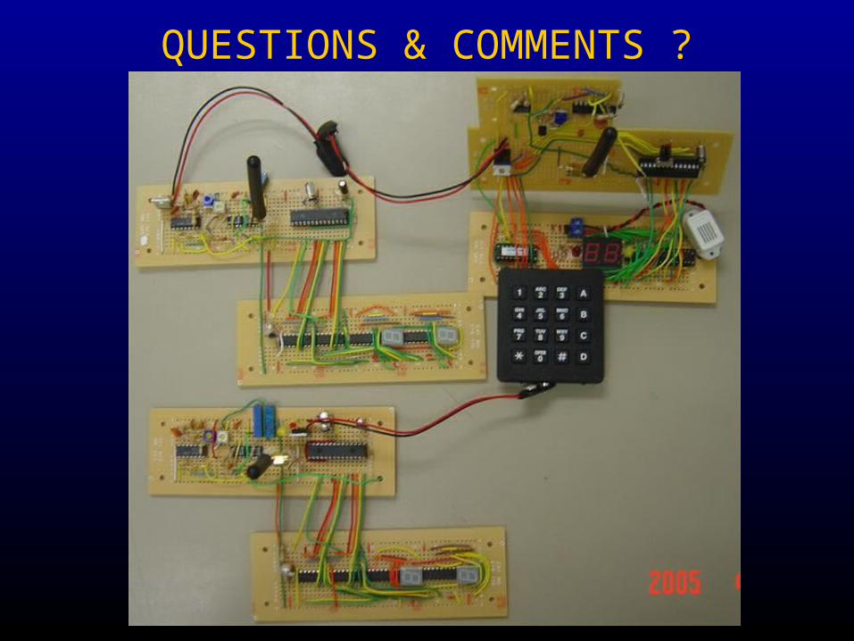
All of our units were tested and demonstrated functional within the allocated time period.
We have constructed and implemented our own FSK receiver and transmitter and completed the system integration by the project demonstration date.
The units are powered by 9V batteries.
Wireless transmission is achieved for a distance of 10cm. During testing we successfully transmitted a distance of 20mm through a partex board.
On a testing trial of 50 times no errors (cross connection) between the two receiving units are observed.
The total project cost is within the proposed budget.
FURTHER IMPROVEMENTS
We down-shifted our carrier frequency from about a MHz to 100kHz to implement a frequency upconverter.
The 1MHz FSK generator implemented with a 555 timer was tested functional.
However, most high frequency components are surface mount and lacking the facilities and time, we were unable to utilize a better frequency range.
As further improvements, a higher frequency carrier will improve range (up to 50 yards with at 100MHz) with no significant increase in power.
Multiple users (receiver units) can be implemented to the current system by simply changing the channel code for each unit for the PIC mcu.
Some error bits were noticed during testing (within the same channel). This can be corrected by implementing Hamming or similar error detection/correction procedures.
QUESTIONS & COMMENTS ?