muri 2001 review experimental study of emp upset ... · muri 2001 review experimental study of emp...
TRANSCRIPT

IREAP
MURI 2001 Review
Experimental Study of EMP Upset Mechanisms in Analogand Digital Circuits
John Rodgers, T. M. Firestone,V. L. Granatstein, M. Walter
Institute for Research in Electronics and Applied PhysicsUniversity of Maryland
College Park, MD 20742

Report Documentation Page Form ApprovedOMB No. 0704-0188
Public reporting burden for the collection of information is estimated to average 1 hour per response, including the time for reviewing instructions, searching existing data sources, gathering andmaintaining the data needed, and completing and reviewing the collection of information. Send comments regarding this burden estimate or any other aspect of this collection of information,including suggestions for reducing this burden, to Washington Headquarters Services, Directorate for Information Operations and Reports, 1215 Jefferson Davis Highway, Suite 1204, ArlingtonVA 22202-4302. Respondents should be aware that notwithstanding any other provision of law, no person shall be subject to a penalty for failing to comply with a collection of information if itdoes not display a currently valid OMB control number.
1. REPORT DATE JUL 2006
2. REPORT TYPE N/A
3. DATES COVERED -
4. TITLE AND SUBTITLE Experimental Study of EMP Upset Mechanisms in Analog and Digital Circuits
5a. CONTRACT NUMBER
5b. GRANT NUMBER
5c. PROGRAM ELEMENT NUMBER
6. AUTHOR(S) 5d. PROJECT NUMBER
5e. TASK NUMBER
5f. WORK UNIT NUMBER
7. PERFORMING ORGANIZATION NAME(S) AND ADDRESS(ES) Institute for Research in Electronics and Applied Physics University ofMaryland College Park, MD 20742
8. PERFORMING ORGANIZATIONREPORT NUMBER
9. SPONSORING/MONITORING AGENCY NAME(S) AND ADDRESS(ES) 10. SPONSOR/MONITOR’S ACRONYM(S)
11. SPONSOR/MONITOR’S REPORT NUMBER(S)
12. DISTRIBUTION/AVAILABILITY STATEMENT Approved for public release, distribution unlimited
13. SUPPLEMENTARY NOTES The original document contains color images.
14. ABSTRACT
15. SUBJECT TERMS
16. SECURITY CLASSIFICATION OF: 17. LIMITATION OF ABSTRACT
UU
18. NUMBEROF PAGES
24
19a. NAME OFRESPONSIBLE PERSON
a. REPORT unclassified
b. ABSTRACT unclassified
c. THIS PAGE unclassified
Standard Form 298 (Rev. 8-98) Prescribed by ANSI Std Z39-18

IREAP
Outline and Motivation• Out-of-band frequency response in communications circuits
– Effect of parasitic elements on network performance– Degradation in filter rejection ratios– EMP propagation on signal path– Need for wideband circuit characterization and verification throughout the
communications network (RF and IF path, mixer, A/D, power vias, etc.)• Experimental study of device upset using direct RF injection
– Identify RF characteristics that produce bit errors, latch-up– What are the EMP effects at the device level?– Modulation and nonlinear circuit response
• Directions to pursue– Experiment– Modeling

IREAP
Schematic of a “loop-back” test circuit for investigating RFeffects in digital communications systems and components
ADC
SAW Filter BP FilterLNA
LO
Mixer
In
Logic
Out
DAC
RAM
LO
Mixer
SAW Filter BP FilterLNA
Probe Probe
Probe
ProbeProbeProbeProbe
Find possible RF entry points, pathways and circuit effectsthat may upset the system or corrupt data.

IREAP
Example: 2 GHz RF LNA
-20
0
20
0 5 10 15
Frequency [GHz]
Gai
n [d
B]
IREAP
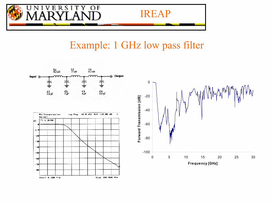
Example: 1 GHz low pass filter
-100
-80
-60
-40
-20
0
0 5 10 15 20 25 30
Frequency [GHz]
Forw
ard
Tran
smis
sion
[dB
]

IREAP
140 MHz IF surface acoustic wave (SAW) filter
-100
-80
-60
-40
-20
0
0 5 10 15 20Frequency [GHz]
Forw
ard
Tran
smis
sion
[dB
]

IREAP
Schematic of direct injection experiment
MicrowaveSynthesizer
RF CouplerAmplifier
Computer
10 dB
Power Meter
A
H
U/D
Reset
B1
B8
Load
Carry out
ENB
DRAM
FET Probe
Digitizer

IREAP
Direct injection test facility

IREAP
View of injection coupler and memorymodules inside computer

IREAP
Memory checking code displaying bit errors

IREAP
RAS logic waveform with andwithout RF injection
• Device no longerlatches to Vdd andVss
• RF changesoperating bias point
• Susceptibility mayinvolve synergisticeffects where RFincreases likelihoodof interference frominternal signals.
Row Addressing Pin on DRAM Panasonic 424100RF applied (1.965 GHz at 26 dBm)
-1
0
1
2
3
4
5
6
0 100 200 300 400 500
Time [ns]
RA
S Vo
ltage
[V]
RAS no RF RAS with RF

IREAP
Frequency spectrum of RAS waveform
0
0.1
0.2
0.3
0.4
0.5
0.6
0.7
10 20 30 40 50 60 70 80 90Frequency [M Hz]
Am
plitu
de
RF onRF off
Clock Frequency= 33 MHz

IREAP
Results with CW injectionThreshold Power to cause Bit Error at RAS pin
Signal Generator Power
-15
-10
-5
0
5
10
1 1.2 1.4 1.6 1.8 2
Frequency (GHz)
Sign
al G
ener
ator
Pow
er (d
Bm
)
CW

IREAP
RAS Voltage vs. time with PulsedRF Injection (f~2 GHz)
RAS Pin with injected RF before interupt1.965 GHz (PW=150 ns, PRI=300 ns, Pin=29.4 dBm)
-1
0
1
2
3
4
5
6
0 100 200 300 400 500
Time (ns)
Volta
ge (V
)
RF Pulse
RAS Logic Pulse

IREAP
Comparison of results with CW and pulsed injection
Threshold Power to cause Bit Error at RAS pin
0
5
10
15
20
25
30
35
40
1 1.2 1.4 1.6 1.8 2 2.2
Frequency [GHz]
Inje
cted
Pow
er [d
Bm
]
Pulse Mod 50% DF CW

IREAP
Amplitude of demodulated RF signal on RAS vs. frequency
0
0.5
1
1.5
2
2.5
3
0 5 10 15 20
Frequency [GHz]
AM
Lev
el [V
]
Frequency range where
upset was observed
IREAP
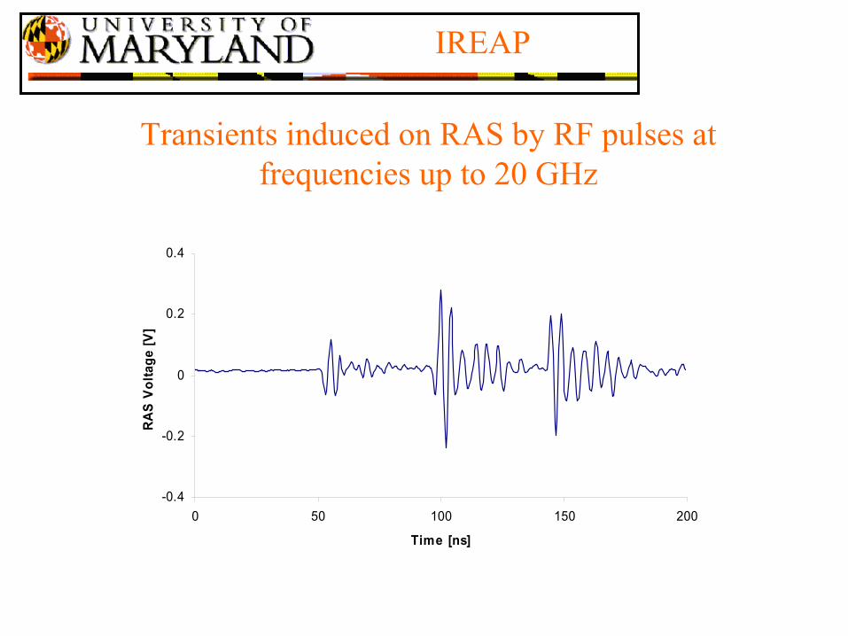
Transients induced on RAS by RF pulses atfrequencies up to 20 GHz
-0.4
-0.2
0
0.2
0.4
0 50 100 150 200
Time [ns]
RAS
Volta
ge [V
]

IREAP
What mechanisms may be responsible for theobserved effects?
• Thermal: localized RF energy deposition and rapid heating ofactive MOS regions
• Hot-carriers• Nonlinear circuit elements
– MOS diodes acting as RF detectors– Demodulation of RF by parametric capacitances

IREAP
Upset threshold power vs. duty factor
-70
-60
-50
-40
-30
-20
-10
0
0.001 0.01 0.1 1 10 100
Duty Factor [%]
Thre
shol
d Up
set P
ower
[dBm
]
Average Injected PowerPeak Injected Power
Not a thermal effect

IREAP
Physical Cross-section of CMOS showing equivalentcircuit elements with nonlinear electrical
characteristics
n well
p- type substrate layer
p well
n+n+ p+p+
SourceContact
DrainContact
DrainContact
SourceContact
Polysilicongate
Polysilicongate
GateOxide
GateOxide
FieldOxide
FieldOxide
FieldOxide
n- epi
R
PMOSNMOS
R
IREAP
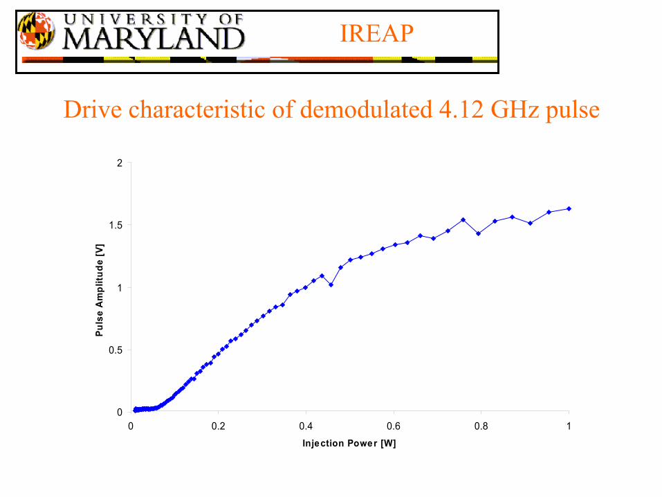
Drive characteristic of demodulated 4.12 GHz pulse
0
0.5
1
1.5
2
0 0.2 0.4 0.6 0.8 1Injection Power [W]
Puls
e A
mpl
itude
[V]

IREAP
Drive characteristic of 6.0 GHz transient pulse
0.01
0.06
0.11
0.16
0.21
0.26
0.31
0.36
0 0.2 0.4 0.6 0.8 1
Injection Power [W]
Puls
e A
mpl
itude
[V]

IREAP
Conclusions
• High frequency response of communications circuits mustbe considered when analyzing susceptibility to determineprobable entry and propagation paths for EMP.
• The RF shifts the operating bias with respect to Vdd andVss into a nonlinear amplification regime, which could leadto instability, oscillation and chaotic behavior.
• RF pulses are demodulated by nonlinear MOS elements.The envelop voltage constitutes the interrupting signal.
• EMP rise time is a key parameter for inducing interruptsignals over wide bandwidths.

IREAP
Future Work
• The experimental results give basis for modeling highfrequency effects in devices
• Continue to characterize device-level upset mechanismsand seek to develop generalized formalisms
• Study the effects of complex modulation• Look at smaller, faster structures (CPU, RDRAM, DDR,
etc.) and investigate how scaling laws may be applied• Investigated RF effects in mixed signal systems (A/D,
demodulators, etc.)