mx29la321m h/l - dataman€¦ · 3 p/n:pm1145 rev. 0.04, mar. 22, 2005 mx29la321m h/l pin...
TRANSCRIPT

1
P/N:PM1145 REV. 0.04, MAR. 22, 2005
MX29LA321M H/L32M-BIT SINGLE VOLTAGE 3V ONLYUNIFORM SECTOR FLASH MEMORY
FEATURES
GENERAL FEATURES• Single Power Supply Operation
- 2.7 to 3.6 volt for read, erase, and program opera-tions
• Configuration- 4,194,304 x 8 / 2,097,152 x 16 switchable
• Sector structure- 64KB(32KW) x 64
• Latch-up protected to 250mA from -1V to VCC + 1V• Low VCC write inhibit is equal to or less than 1.5V• Compatible with JEDEC standard
- Pin-out and software compatible to single power sup-ply Flash
PERFORMANCE• High Performance
- Fast access time: 70R/90ns- Page read time: 25ns- Sector erase time: 0.5s (typ.)- 4 word/8 byte page read buffer- 16 word/ 32 byte write buffer: reduces programmingtime for multiple-word/byte updates
• Low Power Consumption- Active read current: 18mA(typ.)- Active write current: 20mA(typ.)- Standby current: 20uA(typ.)
• Minimum 100,000 erase/program cycle• 20-year data retention
SOFTWARE FEATURES• Supports Common Flash Interface (CFI)
- Flash device parameters stored on the device andprovide the host system to access.
• Program Suspend/Program Resume- Suspend program operation to read other sectors
• Erase Suspend/ Erase Resume- Suspends sector erase operation to read data/pro-gram other sectors
• Status Reply
- Data# polling & Toggle bits provide detection of pro-gram and erase operation completion
HARDWARE FEATURES• Ready/Busy (RY/BY#) Output
- Provides a hardware method of detecting programand erase operation completion
• Hardware Reset (RESET#) Input- Provides a hardware method to reset the internalstate machine to read mode
• WP#/ACC input- Write protect (WP#) function allows protection first orlast sector, regardless of sector protection settings- ACC (high voltage) accelerates programming timefor higher throughput during system
SECURITY• Sector Protection/Chip Unprotect
- Provides sector group protect function to prevent pro-gram or erase operation in the protected sector group- Provides chip unprotect function to allow codechanges- Provides temporary sector group unprotect functionfor code changes in previously protected sector groups
• Sector Permanent Lock- Through a unique permanent locking scheme, thedevice allows the user to permanently lock any ran-domly selected sector(s) within the memory array(Please contact Macronix for specifics relating tothis feature - this datasheet does not include anyother information relating to this feature)
• Secured Silicon Sector- Provides a 128-word OTP area for permanent, se-cure identification- Can be programmed and locked at factory or by cus-tomer
PACKAGE• 56-pin TSOP• 64-ball CSP
GENERAL DESCRIPTION
The MX29LA321M H/L is a 32-mega bit Flash memoryorganized as 4M bytes of 8 bits or 2M words of 16 bits.MXIC's Flash memories offer the most cost-effective andreliable read/write non-volatile random access memory.The MX29LA321M H/L is packaged in 56-pin TSOP and
64-ball CSP. It is designed to be reprogrammed anderased in system or in standard EPROM programmers.
The standard MX29LA321M H/L offers access time asfast as 70ns, allowing operation of high-speed micropro-cessors without wait states. To eliminate bus conten-tion, the MX29LA321M H/L has separate chip enable
PRELIMINARY

2
P/N:PM1145 REV. 0.04, MAR. 22, 2005
MX29LA321M H/L
(CE#) and output enable (OE#) controls.
MXIC's Flash memories augment EPROM functionalitywith in-circuit electrical erasure and programming. TheMX29LA321M H/L uses a command register to managethis functionality.
MXIC Flash technology reliably stores memory contentseven after 100,000 erase and program cycles. The MXICcell is designed to optimize the erase and programmechanisms. In addition, the combination of advancedtunnel oxide processing and low internal electric fieldsfor erase and programming operations produces reliablecycling. The MX29LA321M H/L uses a 2.7V to 3.6VVCC supply to perform the High Reliability Erase andauto Program/Erase algorithms.
The highest degree of latch-up protection is achievedwith MXIC's proprietary non-epi process. Latch-up pro-tection is proved for stresses up to 100 milliamperes onaddress and data pins from -1V to VCC + 1V.
AUTOMATIC PROGRAMMING
The MX29LA321M H/L is byte/word/page programmableusing the Automatic Programming algorithm. The Auto-matic Programming algorithm does not require the exter-nal system to have a time-out sequence nor verificationof the data programmed.
AUTOMATIC PROGRAMMING ALGORITHM
MXIC's Automatic Programming algorithm requires theuser to only write program set-up commands (including 2unlock write cycle and A0H) and a program command(program data and address). The device automaticallytimes the programming pulse width, provides the programverification, and counts the number of sequences. A sta-tus bit similar to DATA# polling and a status bit togglingbetween consecutive read cycles, provide feedback tothe user as to the status of the programming operation.
AUTOMATIC CHIP ERASE
The entire chip is bulk erased using 50 ms erase pulsesaccording to MXIC's Automatic Chip Erase algorithm. TheAutomatic Erase algorithm automatically programs theentire array prior to electrical erase. The timing and veri-
fication of electrical erase are controlled internally withinthe device.
AUTOMATIC SECTOR ERASE
The MX29LA321M H/L is sector(s) erasable using MXIC'sAuto Sector Erase algorithm. Sector erase modes allowsectors of the array to be erased in one erase cycle. TheAutomatic Sector Erase algorithm automatically programsthe specified sector(s) prior to electrical erase. The tim-ing and verification of electrical erase are controlled inter-nally within the device.
AUTOMATIC ERASE ALGORITHM
MXIC's Automatic Erase algorithm requires the user towrite commands to the command register using stan-dard microprocessor write timings. The device will auto-matically pre-program and verify the entire array. Thenthe device automatically times the erase pulse width,provides the erase verification, and counts the numberof sequences. A status bit toggling between consecu-tive read cycles provides feedback to the user as to thestatus of the programming operation.
Register contents serve as inputs to an internal state-machine which controls the erase and programming cir-cuitry. During write cycles, the command register inter-nally latches address and data needed for the program-ming and erase operations. During a system write cycle,addresses are latched on the falling edge, and data arelatched on the rising edge of WE# .
MXIC's Flash technology combines years of EPROMexperience to produce the highest levels of quality, reli-ability, and cost effectiveness. The MX29LA321M H/Lelectrically erases all bits simultaneously using Fowler-Nordheim tunneling. The bytes are programmed by us-ing the EPROM programming mechanism of hot elec-tron injection.
During a program cycle, the state-machine will controlthe program sequences and command register will notrespond to any command set. During a Sector Erasecycle, the command register will only respond to EraseSuspend command. After Erase Suspend is completed,the device stays in read mode. After the state machinehas completed its task, it will allow the command regis-ter to respond to its full command set.

3
P/N:PM1145 REV. 0.04, MAR. 22, 2005
MX29LA321M H/L
PIN CONFIGURATION
56 TSOP
64 CSP
NCCE1A21A20A19A18A17A16
VDDA15A14A13A12CE0
WP#/ACCRESET#
A11A10A9A8
VSSA7A6A5A4A3A2A1
12345678910111213141516171819202122232425262728
NCWE#OE#RY/BY#Q15Q7Q14Q6VSSS13Q5Q12Q4VCCGNDQ11Q3Q10Q2VDDQ9Q1Q8Q0A0BYTE#NCCE2
56555453525150494847464544434241403938373635343332313029
1 2 3 4 5 6 7 8
A1A
B
C
D
E
F
G
H
A6 A8 WP#/ACC
A13 VCC A18 NC
A2 GND A9 CE0 A14 NC A19 CE1
A3 A7 A10 A12 A15 NC A20 A21
A4 A5 A11 RES-ET#
NC NC A16 A17
Q8 Q1 Q9 Q3 Q4 NC Q15 RY/BY#
BYTE# Q0 Q10 Q11 Q12 NC NC OE#
NC A0 Q2 VCC Q5 Q6 Q14 WE#
CE2 NC VDD GND Q13 GND Q7 NC

4
P/N:PM1145 REV. 0.04, MAR. 22, 2005
MX29LA321M H/L
SYMBOL PIN NAME
A0 Byte-Select Address
A1~A21 Address Input
Q0~Q15 Data Inputs/Outputs
CE# Chip Enable Input
WE# Write Enable Input
OE# Output Enable Input
RESET# Hardware Reset Pin, Active Low
WP#/ACC Hardware Write Protect/Programming
Acceleration input
RY/BY# Read/Busy Output
BYTE# Selects 8 bit or 16 bit mode
VCC +3.0V single power supply
VI/O Output Buffer Power (This input should
be tied directly to VCC 2.7V~3.6V)
GND Device Ground
NC Pin Not Connected Internally
PIN DESCRIPTION LOGIC SYMBOL
Chip Enable Truth Table
CE2 CE1 CE0 DEVICE
VIL VIL VIL Enabled
VIL VIL VIH Disabled
VIL VIH VIL Disabled
VIL VIH VIH Disabled
VIH VIL VIL Enabled
VIH VIL VIH Enabled
VIH VIH VIL Enabled
VIH VIH VIH Disabled
Note: For Single-chip applications, CE2 and CE1 can bestrapped to GND.
16 or 8Q0-Q15
(A-1)
RY/BY#
A0-A21
CE#
OE#
WE#
RESET#
WP#/ACC
BYTE#
VI/O
22
5
P/N:PM1145 REV. 0.04, MAR. 22, 2005
MX29LA321M H/L
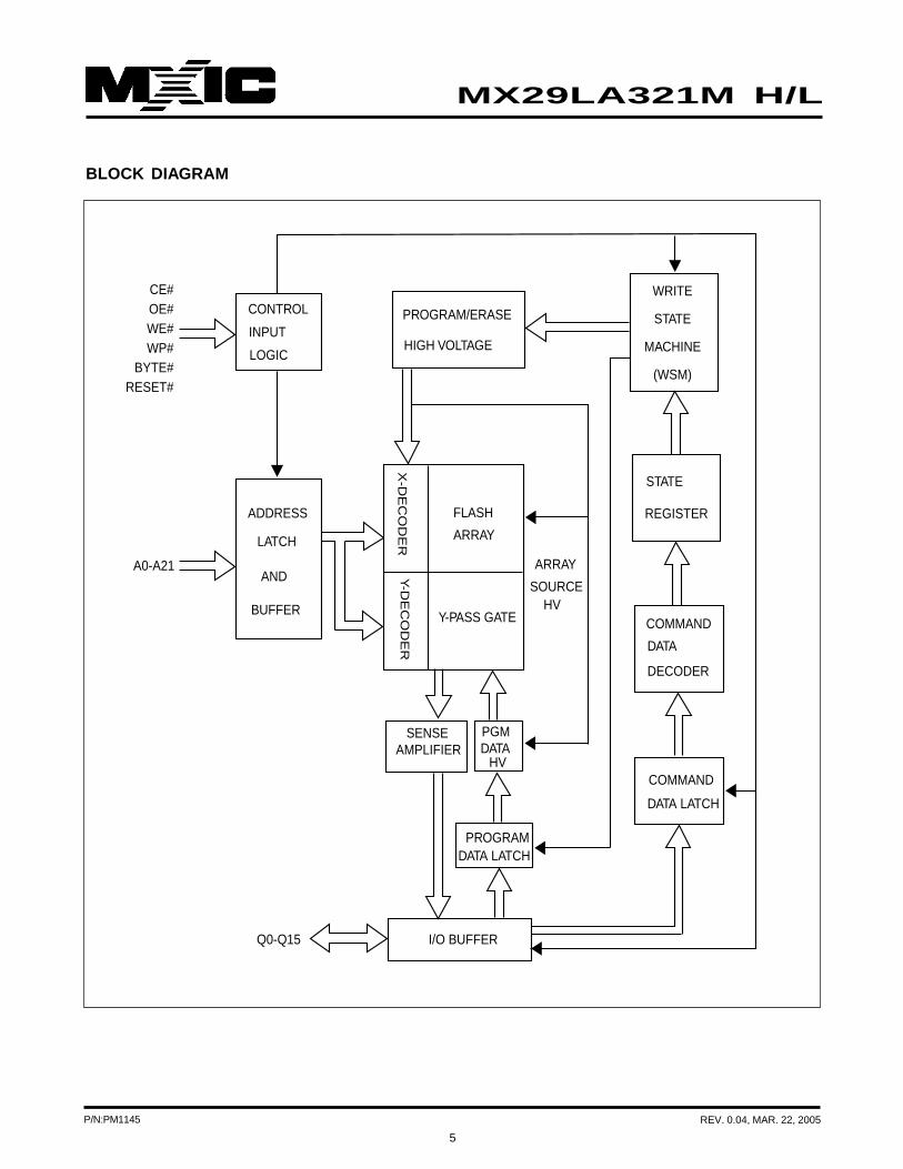
BLOCK DIAGRAM
CONTROL
INPUT
LOGIC
PROGRAM/ERASE
HIGH VOLTAGE
WRITE
STATE
MACHINE
(WSM)
STATE
REGISTERFLASH
ARRAY
X-D
EC
OD
ER
ADDRESS
LATCH
AND
BUFFER Y-PASS GATE
Y-D
EC
OD
ER
ARRAY
SOURCEHV
COMMAND
DATA
DECODER
COMMAND
DATA LATCH
I/O BUFFER
PGMDATA
HV
PROGRAMDATA LATCH
SENSEAMPLIFIER
Q0-Q15
A0-A21
CE#OE#WE#WP#
BYTE#RESET#

6
P/N:PM1145 REV. 0.04, MAR. 22, 2005
MX29LA321M H/L
Sector Sector Address Sector Size (x8) (x16)
A21-A16 (Kbytes/Kwords) Address Range Address Range
SA0 000000 64/32 000000-0FFFF 000000-07FFF
SA1 000001 64/32 010000-1FFFF 008000-0FFFF
SA2 000010 64/32 020000-2FFFF 010000-17FFF
SA3 000011 64/32 030000-3FFFF 018000-1FFFF
SA4 000100 64/32 040000-4FFFF 020000-27FFF
SA5 000101 64/32 050000-5FFFF 028000-2FFFF
SA6 000110 64/32 060000-6FFFF 030000-37FFF
SA7 000111 64/32 070000-7FFFF 038000-3FFFF
SA8 001000 64/32 080000-8FFFF 040000-47FFF
SA9 001001 64/32 090000-9FFFF 048000-4FFFF
SA10 001010 64/32 0A0000-AFFFF 050000-57FFF
SA11 001011 64/32 0B0000-BFFFF 058000-5FFFF
SA12 001100 64/32 0C0000-CFFFF 060000-67FFF
SA13 001101 64/32 0D0000-DFFFF 068000-6FFFF
SA14 001110 64/32 0E0000-EFFFF 070000-77FFF
SA15 001111 64/32 0F0000-FFFFF 078000-7FFFF
SA16 010000 64/32 100000-0FFFF 080000-87FFF
SA17 010001 64/32 110000-1FFFF 088000-8FFFF
SA18 010010 64/32 120000-2FFFF 090000-97FFF
SA19 010011 64/32 130000-3FFFF 098000-9FFFF
SA20 010100 64/32 140000-4FFFF 0A0000-A7FFF
SA21 010101 64/32 150000-5FFFF 0A8000-AFFFF
SA22 010110 64/32 160000-6FFFF 0B0000-B7FFF
SA23 010111 64/32 170000-7FFFF 0B8000-BFFFF
SA24 011000 64/32 180000-8FFFF 0C0000-C7FFF
SA25 011001 64/32 190000-9FFFF 0C8000-CFFFF
SA26 011010 64/32 1A0000-AFFFF 0D0000-D7FFF
SA27 011011 64/32 1B0000-BFFFF 0D8000-DFFFF
SA28 011100 64/32 1C0000-CFFFF 0E0000-E7FFF
SA29 011101 64/32 1D0000-DFFFF 0E8000-EFFFF
SA30 011110 64/32 1E0000-EFFFF 0F0000-F7FFF
SA31 011111 64/32 1F0000-FFFFF 0F8000-FFFFF
MX29LA321M H/L SECTOR ADDRESS TABLE

7
P/N:PM1145 REV. 0.04, MAR. 22, 2005
MX29LA321M H/L
Sector Sector Address Sector Size (x8) (x16)
A21-A16 (Kbytes/Kwords) Address Range Address Range
SA32 100000 64/32 200000-0FFFF 100000-07FFF
SA33 100001 64/32 210000-1FFFF 108000-0FFFF
SA34 100010 64/32 220000-2FFFF 110000-17FFF
SA35 100011 64/32 230000-3FFFF 118000-1FFFF
SA36 100100 64/32 240000-4FFFF 120000-27FFF
SA37 100101 64/32 250000-5FFFF 128000-2FFFF
SA38 100110 64/32 260000-6FFFF 130000-37FFF
SA39 100111 64/32 270000-7FFFF 138000-3FFFF
SA40 101000 64/32 280000-8FFFF 140000-47FFF
SA41 101001 64/32 290000-9FFFF 148000-4FFFF
SA42 101010 64/32 2A0000-AFFFF 150000-57FFF
SA43 101011 64/32 2B0000-BFFFF 158000-5FFFF
SA44 101100 64/32 2C0000-CFFFF 160000-67FFF
SA45 101101 64/32 2D0000-DFFFF 168000-6FFFF
SA46 101110 64/32 2E0000-EFFFF 170000-77FFF
SA47 101111 64/32 2F0000-FFFFF 178000-7FFFF
SA48 110000 64/32 300000-0FFFF 180000-87FFF
SA49 110001 64/32 310000-1FFFF 188000-8FFFF
SA50 110010 64/32 320000-2FFFF 190000-97FFF
SA51 110011 64/32 330000-3FFFF 198000-9FFFF
SA52 110100 64/32 340000-4FFFF 1A0000-A7FFF
SA53 110101 64/32 350000-5FFFF 1A8000-AFFFF
SA54 110110 64/32 360000-6FFFF 1B0000-B7FFF
SA55 110111 64/32 370000-7FFFF 1B8000-BFFFF
SA56 111000 64/32 380000-8FFFF 1C0000-C7FFF
SA57 111001 64/32 390000-9FFFF 1C8000-CFFFF
SA58 111010 64/32 3A0000-AFFFF 1D0000-D7FFF
SA59 111011 64/32 3B0000-BFFFF 1D8000-DFFFF
SA60 111100 64/32 3C0000-CFFFF 1E0000-E7FFF
SA61 111101 64/32 3D0000-DFFFF 1E8000-EFFFF
SA62 111110 64/32 3E0000-EFFFF 1F0000-F7FFF
SA63 111111 64/32 3F0000-FFFFF 1F8000-FFFFF
8
P/N:PM1145 REV. 0.04, MAR. 22, 2005
MX29LA321M H/L
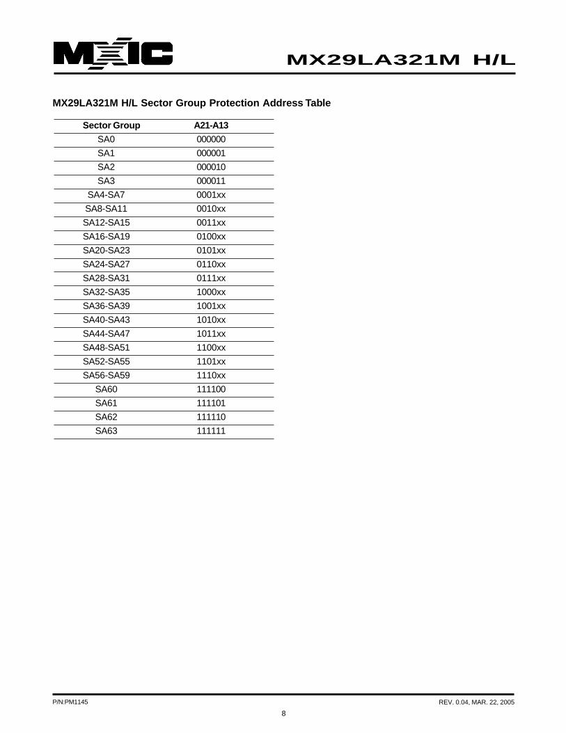
MX29LA321M H/L Sector Group Protection Address Table
Sector Group A21-A13
SA0 000000
SA1 000001
SA2 000010
SA3 000011
SA4-SA7 0001xx
SA8-SA11 0010xx
SA12-SA15 0011xx
SA16-SA19 0100xx
SA20-SA23 0101xx
SA24-SA27 0110xx
SA28-SA31 0111xx
SA32-SA35 1000xx
SA36-SA39 1001xx
SA40-SA43 1010xx
SA44-SA47 1011xx
SA48-SA51 1100xx
SA52-SA55 1101xx
SA56-SA59 1110xx
SA60 111100
SA61 111101
SA62 111110
SA63 111111

9
P/N:PM1145 REV. 0.04, MAR. 22, 2005
MX29LA321M H/L
Q8~Q15
Operation CE# OE# WE# RE- WP# ACC Address Q0~Q7 Word Byte
SET# Mode Mode
Read L L H H X X AIN DOUT DOUT Q8-Q15=
High Z
Write (Program/Erase) L H L H (Note 3) X AIN (Note 4) (Note 4 Q8-Q15=
High Z
Accelerated Program L H L H (Note 3) VHH AIN (Note 4) (Note 4) Q8-Q15=
High Z
Standby VCC± X X VCC± X H X High-Z High-Z High-Z
0.3V 0.3V
Output Disable L H H H X X X High-Z High-Z High-Z
Reset X X X L X X X High-Z High-Z High-Z
Sector Group Protect L H L VID H X Sector Addresses, (Note 4) X X
(Note 2) A7=L,A4=L, A3=L,
A2=H,A1=L
Chip unprotect L H L VID H X Sector Addresses, (Note 4) X X
(Note 2) A7=H, A4=L, A3=L,
A2=H, A1=L
Temporary Sector X X X VID H X AIN (Note 4) (Note 4) High-Z
Group Unprotect
Legend:L=Logic LOW=V
IL, H=Logic High=V
IH, V
ID=12.0±0.5V, V
HH=12.0±0.5V, X=Don't Care, A
IN=Address IN, D
IN=Data IN,
DOUT
=Data OUT
Notes:1. Address are A21:A1 in word mode; A21:A0 in byte mode. Sector addresses are A21:A14 in both modes.2. The sector group protect and chip unprotect functions may also be implemented via programming equipment. See
the "Sector Group Protection and Chip Unprotect" section.3. If WP#=VIL, the first sectors remain protected. If WP#=VIH, the first or last sector protection depends on whether
they were last protected or unprotect using the method described in "Sector/ Sector Block Protection and Unprotect".4. DIN or DOUT as required by command sequence, Data# polling or sector protect algorithm (see Table 3 and Figure 15).
Table 1. BUS OPERATION (1)

10
P/N:PM1145 REV. 0.04, MAR. 22, 2005
MX29LA321M H/L
Table 2. AUTOSELECT CODES (High Voltage Method)
A21 A15 A9 A6 A4 Q8 to Q15
Description CE# OE# WE# to to A10 to A7 to to A2 A1 Word Byte Q7 to Q0
A16 A11 A8 A5 A3 Mode Mode
Manufacturer ID L L H X X VID X L X L L L 00 X C2h
Cycle 1 L L H 22 X 7Eh
Cycle 2 L L H X X VID X L X H H L 22 X 1Dh
Cycle 3 H H H 22 X 00h
Sector Group 01h (protected),
Protection L L H SA X VID X L X L H L X X
Verification 00h (unprotected)
Secured Silicon 98h
Sector Indicator (factory locked),
Bit (Q7), WP# L L H X X VID X L X L H H X X
protects highest 18h
address sector (not factory locked)
Secured Silicon 88h
Sector Indicator (factory locked),
Bit (Q7), WP# L L H X X VID X L X L H H X X
protects lowest 08h
address sector (not factory locked)
Legend: L = Logic Low = VIL, H = Logic High = VIH, SA = Sector Address, X = Don't care.
29LA
321M
H/L

11
P/N:PM1145 REV. 0.04, MAR. 22, 2005
MX29LA321M H/L
REQUIREMENTS FOR READING ARRAYDATA
To read array data from the outputs, the system mustdrive the CE# and OE# pins to VIL. CE# is the powercontrol and selects the device. OE# is the output controland gates array data to the output pins. WE# should re-main at VIH.
The internal state machine is set for reading array dataupon device power-up, or after a hardware reset. Thisensures that no spurious alteration of the memory con-tent occurs during the power transition. No command isnecessary in this mode to obtain array data. Standardmicroprocessor read cycles that assert valid address onthe device address inputs produce valid data on the de-vice data outputs. The device remains enabled for readaccess until the command register contents are altered.
PAGE MODE READ
The MX29LA321M H/L offers "fast page mode read" func-tion. This mode provides faster read access speed forrandom locations within a page. The page size of thedevice is 4 words/8 bytes. The appropriate page is se-lected by the higher address bits A1~A2(Word Mode)/A0~A2(Byte Mode) This is an asynchronous operation;the microprocessor supplies the specific word location.
The system performance could be enhanced by initiating1 normal read and 3 fast page read (for word mode A1-A2) or 7 fast page read (for byte mode A0~A2). WhenCE# is deasserted and reasserted for a subsequent ac-cess, the access time is tACC or tCE. Fast page modeaccesses are obtained by keeping the "read-page ad-dresses" constant and changing the "intra-read page"addresses.
WRITING COMMANDS/COMMAND SE-QUENCES
To program data to the device or erase sectors of memory,the system must drive WE# and CE# to VIL, and OE# toVIH.
An erase operation can erase one sector, multiple sec-tors, or the entire device. The Sector Address Table onpage 6 and 7 indicates the address space that eachsector occupies. A "sector address" consists of the ad-
dress bits required to uniquely select a sector. The "Writ-ing specific address and data commands or sequencesinto the command register initiates device operations.Table 3 defines the valid register command sequences.Writing incorrect address and data values or writing themin the improper sequence resets the device to readingarray data. Section has details on erasing a sector or theentire chip, or suspending/resuming the erase operation.
After the system writes the Automatic Select commandsequence, the device enters the Automatic Select mode.The system can then read Automatic Select codes fromthe internal register (which is separate from the memoryarray) on Q7-Q0. Standard read cycle timings apply inthis mode. Refer to the Automatic Select Mode and Au-tomatic Select Command Sequence section for moreinformation.
ICC2 in the DC Characteristics table represents the ac-tive current specification for the write mode. The "ACCharacteristics" section contains timing specificationtable and timing diagrams for write operations.
WRITE BUFFER
Write Buffer Programming allows the system to write amaximum of 16 words/32 bytes in one programming op-eration. This results in faster effective programming timethan the standard programming algorithms. See "WriteBuffer" for more information.
ACCELERATED PROGRAM OPERATION
The device offers accelerated program operations throughthe ACC function. This is one of two functions providedby the ACC pin. This function is primarily intended toallow faster manufacturing throughput at the factory.
If the system asserts VHH on this pin, the device auto-matically enters the aforementioned Unlock Bypassmode, temporarily unprotects any protected sectors, anduses the higher voltage on the pin to reduce the timerequired for program operations. The system would usea two-cycle program command sequence as required bythe Unlock Bypass mode. Removing VHH from the ACCpin must not be at VHH for operations other than accel-erated programming, or device damage may result.

12
P/N:PM1145 REV. 0.04, MAR. 22, 2005
MX29LA321M H/L
STANDBY MODE
When using both pins of CE# and RESET#, the deviceenter CMOS Standby with both pins held at VCC ± 0.3V.If CE# and RESET# are held at VIH, but not within therange of VCC ± 0.3V, the device will still be in the standbymode, but the standby current will be larger. During AutoAlgorithm operation, VCC active current (ICC2) is requiredeven CE# = "H" until the operation is completed. Thedevice can be read with standard access time (tCE) fromeither of these standby modes, before it is ready to readdata.
AUTOMATIC SLEEP MODE
The automatic sleep mode minimizes Flash device en-ergy consumption. The device automatically enables thismode when address remain stable for tACC+30ns. Theautomatic sleep mode is independent of the CE#, WE#,and OE# control signals. Standard address access tim-ings provide new data when addresses are changed. Whilein sleep mode, output data is latched and always avail-able to the system. ICC4 in the DC Characteristics tablerepresents the automatic sleep mode current specifica-tion.
OUTPUT DISABLE
With the OE# input at a logic high level (VIH), outputfrom the devices are disabled. This will cause the outputpins to be in a high impedance state.
RESET# OPERATION
The RESET# pin provides a hardware method of resettingthe device to reading array data. When the RESET# pinis driven low for at least a period of tRP, the deviceimmediately terminates any operation in progress,tristates all output pins, and ignores all read/writecommands for the duration of the RESET# pulse. Thedevice also resets the internal state machine to readingarray data. The operation that was interrupted should bereinitiated once the device is ready to accept anothercommand sequence, to ensure data integrity
Current is reduced for the duration of the RESET# pulse.When RESET# is held at VSS±0.3V, the device drawsCMOS standby current (ICC4). If RESET# is held at VILbut not within VSS±0.3V, the standby current will be
greater.
The RESET# pin may be tied to system reset circuitry.A system reset would that also reset the Flash memory,enabling the system to read the boot-up firmware fromthe Flash memory.
If RESET# is asserted during a program or eraseoperation, the RY/BY# pin remains a "0" (busy) until theinternal reset operation is complete, which requires a timeof tREADY (during Embedded Algorithms). The systemcan thus monitor RY/BY# to determine whether the resetoperation is complete. If RESET# is asserted when aprogram or erase operation is completed within a time oftREADY (not during Embedded Algorithms). The systemcan read data tRH after the RESET# pin returns to VIH.
Refer to the AC Characteristics tables for RESET#parameters and to Figure 3 for the timing diagram.
SECTOR GROUP PROTECT OPERATION
The MX29LA321M H/L features hardware sector groupprotection. This feature will disable both program anderase operations for these sector group protected. Inthis device, a sector group consists of four adjacent sec-tors which are protected or unprotected at the same time(See "MX29LA321M H/L Sector Group Protection AddressTable" on page 8). To activate this mode, the program-ming equipment must force VID on address pin A10 andcontrol pin OE#, (suggest VID = 12V) A7 = VIL and CE#= VIL. (see Table 2) Programming of the protection cir-cuitry begins on the falling edge of the WE# pulse and isterminated on the rising edge. Please refer to sectorgroup protect algorithm and waveform.
MX29LA321M H/L also provides another method. Whichrequires VID on the RESET# only. This method can beimplemented either in-system or via programming equip-ment. This method uses standard microprocessor buscycle timing.
To verify programming of the protection circuitry, the pro-gramming equipment must force VID on address pin A10(with CE# and OE# at VIL and WE# at VIH). When A2=1,it will produce a logical "1" code at device output Q0 for aprotected sector. Otherwise the device will produce 00Hfor the unprotected sector. In this mode, the addresses,except for A2, are don't care. Address locations with A2= VIL are reserved to read manufacturer and device codes.(Read Silicon ID)

13
P/N:PM1145 REV. 0.04, MAR. 22, 2005
MX29LA321M H/L
It is also possible to determine if the group is protectedin the system by writing a Read Silicon ID command.Performing a read operation with A2=VIH, it will producea logical "1" at Q0 for the protected sector.
CHIP UNPROTECT OPERATION
The MX29LA321M H/L also features the chip unprotectmode, so that all sectors are unprotected after chipunprotect is completed to incorporate any changes inthe code. It is recommended to protect all sectors beforeactivating chip unprotect mode.
To activate this mode, the programming equipment mustforce VID on control pin OE# and address pin A10. TheCE# pins must be set at VIL. Pins A7 must be set toVIH. (see Table 2) Refer to chip unprotect algorithm andwaveform for the chip unprotect algorithm. The unprotectmechanism begins on the falling edge of the WE# pulseand is terminated on the rising edge.
MX29LA321M H/L also provides another method. Whichrequires VID on the RESET# only. This method can beimplemented either in-system or via programming equip-ment. This method uses standard microprocessor buscycle timing.
It is also possible to determine if the chip is unprotect inthe system by writing the Read Silicon ID command.Performing a read operation with A2=VIH, it will produce00H at data outputs (Q0-Q7) for an unprotect sector. It isnoted that all sectors are unprotected after the chipunprotect algorithm is completed.
WRITE PROTECT (WP#)
The write protect function provides a hardware methodto protect sector without using V
ID.
If the system asserts VIL on the WP# pin, the devicedisables program and erase functions in the first(MX29LA321MH) or last (MX29LA321ML) sector inde-pendently of whether those sectors were protected orunprotect using the method described in Sector/SectorGroup Protection and Chip Unprotect".
If the system asserts VIH on the WP# pin, the devicereverts to whether the first (MX29LA321MH) or last(MX29LA321ML) sector were last set to be protected or
unprotect. That is, sector protection or unprotection forthese two sectors depends on whether they were lastprotected or unprotect using the method described in"Sector/Sector Group Protection and Chip Unprotect".
Note that the WP# pin must not be left floating or uncon-nected; inconsistent behavior of the device may result.
TEMPORARY SECTOR GROUP UNPROTECTOPERATION
This feature allows temporary unprotect of previouslyprotected sector to change data in-system. The Tempo-rary Sector Unprotect mode is activated by setting theRESET# pin to VID(11.5V-12.5V). During this mode, for-merly protected sectors can be programmed or erasedas unprotect sector. Once VID is remove from the RE-SET# pin, all the previously protected sectors are pro-tected again.
SILICON ID READ OPERATION
Flash memories are intended for use in applications wherethe local CPU alters memory contents. As such, manu-facturer and device codes must be accessible while thedevice resides in the target system. PROM program-mers typically access signature codes by raising A10 toa high voltage. However, multiplexing high voltage ontoaddress lines is not generally desired system design prac-tice.
MX29LA321M H/L provides hardware method to accessthe silicon ID read operation. Which method requires VIDon A10 pin, VIL on CE#, OE#, A7, and A2 pins. Whichapply VIL on A1 pin, the device will output MXIC's manu-facture code of which apply VIH on A1 pin, the device willoutput MX29LA321M H/L device code.
VERIFY SECTOR GROUP PROTECT STATUSOPERATION
MX29LA321M H/L provides hardware method for sectorgroup protect status verify. Which method requires VIDon A10 pin, VIH on WE# and A2 pins, VIL on CE#, OE#,A7, and A1 pins, and sector address on A17 to A22 pins.Which the identified sector is protected, the device willoutput 01H. Which the identified sector is not protect, thedevice will output 00H.
14
P/N:PM1145 REV. 0.04, MAR. 22, 2005
MX29LA321M H/L
DATA PROTECTION
The MX29LA321M H/L is designed to offer protectionagainst accidental erasure or programming caused byspurious system level signals that may exist during powertransition. During power up the device automatically re-sets the state machine in the Read mode. In addition,with its control register architecture, alteration of thememory contents only occurs after successful comple-tion of specific command sequences. The device alsoincorporates several features to prevent inadvertent writecycles resulting from VCC power-up and power-down tran-sition or system noise.
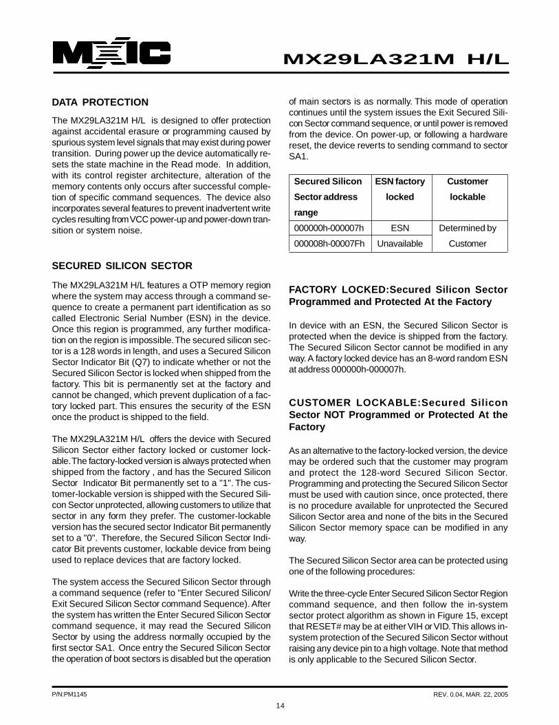
SECURED SILICON SECTOR
The MX29LA321M H/L features a OTP memory regionwhere the system may access through a command se-quence to create a permanent part identification as socalled Electronic Serial Number (ESN) in the device.Once this region is programmed, any further modifica-tion on the region is impossible. The secured silicon sec-tor is a 128 words in length, and uses a Secured SiliconSector Indicator Bit (Q7) to indicate whether or not theSecured Silicon Sector is locked when shipped from thefactory. This bit is permanently set at the factory andcannot be changed, which prevent duplication of a fac-tory locked part. This ensures the security of the ESNonce the product is shipped to the field.
The MX29LA321M H/L offers the device with SecuredSilicon Sector either factory locked or customer lock-able. The factory-locked version is always protected whenshipped from the factory , and has the Secured SiliconSector Indicator Bit permanently set to a "1". The cus-tomer-lockable version is shipped with the Secured Sili-con Sector unprotected, allowing customers to utilize thatsector in any form they prefer. The customer-lockableversion has the secured sector Indicator Bit permanentlyset to a "0". Therefore, the Secured Silicon Sector Indi-cator Bit prevents customer, lockable device from beingused to replace devices that are factory locked.
The system access the Secured Silicon Sector througha command sequence (refer to "Enter Secured Silicon/Exit Secured Silicon Sector command Sequence). Afterthe system has written the Enter Secured Silicon Sectorcommand sequence, it may read the Secured SiliconSector by using the address normally occupied by thefirst sector SA1. Once entry the Secured Silicon Sectorthe operation of boot sectors is disabled but the operation
of main sectors is as normally. This mode of operationcontinues until the system issues the Exit Secured Sili-con Sector command sequence, or until power is removedfrom the device. On power-up, or following a hardwarereset, the device reverts to sending command to sectorSA1.
Secured Silicon ESN factory Customer
Sector address locked lockable
range
000000h-000007h ESN Determined by
000008h-00007Fh Unavailable Customer
FACTORY LOCKED:Secured Silicon SectorProgrammed and Protected At the Factory
In device with an ESN, the Secured Silicon Sector isprotected when the device is shipped from the factory.The Secured Silicon Sector cannot be modified in anyway. A factory locked device has an 8-word random ESNat address 000000h-000007h.
CUSTOMER LOCKABLE:Secured SiliconSector NOT Programmed or Protected At theFactory
As an alternative to the factory-locked version, the devicemay be ordered such that the customer may programand protect the 128-word Secured Silicon Sector.Programming and protecting the Secured Silicon Sectormust be used with caution since, once protected, thereis no procedure available for unprotected the SecuredSilicon Sector area and none of the bits in the SecuredSilicon Sector memory space can be modified in anyway.
The Secured Silicon Sector area can be protected usingone of the following procedures:
Write the three-cycle Enter Secured Silicon Sector Regioncommand sequence, and then follow the in-systemsector protect algorithm as shown in Figure 15, exceptthat RESET# may be at either VIH or VID. This allows in-system protection of the Secured Silicon Sector withoutraising any device pin to a high voltage. Note that methodis only applicable to the Secured Silicon Sector.

15
P/N:PM1145 REV. 0.04, MAR. 22, 2005
MX29LA321M H/L
Write the three-cycle Enter Secured Silicon Sector Regioncommand sequence, and then alternate method of sectorprotection described in the :Sector Group Protection andUnprotect" section.
Once the Secured Silicon Sector is programmed, lockedand verified, the system must write the Exit SecuredSilicon Sector Region command sequence to return toreading and writing the remainder of the array.
LOW VCC WRITE INHIBIT
When VCC is less than VLKO the device does not ac-cept any write cycles. This protects data during VCCpower-up and power-down. The command register andall internal program/erase circuits are disabled, and thedevice resets. Subsequent writes are ignored until VCCis greater than VLKO. The system must provide the propersignals to the control pins to prevent unintentional writewhen VCC is greater than VLKO.
WRITE PULSE "GLITCH" PROTECTION
Noise pulses of less than 5ns (typical) on CE# or WE#will not initiate a write cycle.
LOGICAL INHIBIT
Writing is inhibited by holding any one of OE# = VIL,CE# = VIH or WE# = VIH. To initiate a write cycle CE#and WE# must be a logical zero while OE# is a logicalone.
POWER-UP SEQUENCE
The MX29LA321M H/L powers up in the Read only mode.In addition, the memory contents may only be alteredafter successful completion of the predefined commandsequences.
POWER-UP WRITE INHIBIT
If WE#=CE#=VIL and OE#=VIH during power up, thedevice does not accept commands on the rising edge ofWE#. The internal state machine is automatically resetto the read mode on power-up.
POWER SUPPLY DE COUPLING
In order to reduce power switching effect, each deviceshould have a 0.1uF ceramic capacitor connected be-tween its VCC and GND.

16
P/N:PM1145 REV. 0.04, MAR. 22, 2005
MX29LA321M H/L
TABLE 3. MX29LA321M H/L COMMAND DEFINITIONS
First Bus Second Bus Third Bus Fourth Bus Fifth Bus Sixth Bus
Command Bus Cycle Cycle Cycle Cycle Cycle Cycle
Cycles Addr Data Addr Data Addr Data Addr Data Addr Data Addr Data
Read (Note 5) 1 RA RD
Reset (Note 6) 1 XXX F0
Automatic Select (Note 7)
Manufacturer ID Word 4 555 AA 2AA 55 555 90 X00 C2H
Byte 4 AAA AA 555 55 AAA 90 X00 C2H
Device ID Word 4 555 AA 2AA 55 555 90 X01 ID1 X0E ID2 X0F ID3
(Note 8) Byte 4 AAA AA 555 55 AAA 90 X02 ID1 X1C ID2 X1E ID3
Secured Sector Fact- Word 4 555 AA 2AA 55 555 90 X03 see
ory Protect (Note 9) Byte 4 AAA AA 555 55 AAA 90 X06 Note 9
Sector Group Protect Word 4 555 AA 2AA 55 555 90 (SA)X02 XX00/
Verify (Note 10) Byte 4 AAA AA 555 55 AAA 90 (SA)X04 XX01
Enter Secured Silicon Word 3 555 AA 2AA 55 555 88
Sector Byte 3 AAA AA 555 55 AAA 88
Exit Secured Silicon Word 4 555 AA 2AA 55 555 90 XXX 00
Sector Byte 4 AAA AA 555 55 AAA 90 XXX 00
Program Word 4 555 AA 2AA 55 555 A0 PA PD
Byte 4 AAA AA 555 55 AAA A0 PA PD
Write to Buffer (Note 11) Word 6 555 AA 2AA 55 SA 25 SA WC PA PD WBL PD
Byte 6 AAA AA 555 55 SA 25 SA BC PA PD WBL PD
Program Buffer to Flash Word 1 SA 29
Byte 1 SA 29
Write to Buffer Abort Word 3 555 AA 2AA 55 555 F0
Reset (Note 12) Byte 3 AAA AA 555 55 AAA F0
Chip Erase Word 6 555 AA 2AA 55 555 80 555 AA 2AA 55 555 10
Byte 6 AAA AA 555 55 AAA 80 AAA AA 555 55 AAA 10
Sector Erase Word 6 555 AA 2AA 55 555 80 555 AA 2AA 55 SA 30
Byte 6 AAA AA 555 55 AAA 80 AAA AA 555 55 SA 30
Program/Erase Suspend (Note 13) 1 XXX B0
Program/Erase Resume (Note 14) 1 XXX 30
CFI Query (Note 15) Word 1 55 98
Byte 1 AA 98
SOFTWARE COMMAND DEFINITIONS
Device operations are selected by writing specific ad-dress and data sequences into the command register.Writing incorrect address and data values or writing themin the improper sequence will reset the device to theread mode. Table 3 defines the valid register commandsequences. Note that the Erase Suspend (B0H) and
Erase Resume (30H) commands are valid only while theSector Erase operation is in progress. Either of the tworeset command sequences will reset the device (whenapplicable).
All addresses are latched on the falling edge of WE# orCE#, whichever happens later. All data are latched onrising edge of WE# or CE#, whichever happens first.

17
P/N:PM1145 REV. 0.04, MAR. 22, 2005
MX29LA321M H/L
Notes:1. See Table 1 for descriptions of bus operations.2. All values are in hexadecimal.3. Except when reading array or automatic select data, all bus cycles are write operation.4. Address bits are don't care for unlock and command cycles, except when PA or SA is required.5. No unlock or command cycles required when device is in read mode.6. The Reset command is required to return to the read mode when the device is in the automatic select mode or if
Q5 goes high.7. The fourth cycle of the automatic select command sequence is a read cycle.8. The device ID must be read in three cycles. The data is 01h for top boot and 00h for bottom boot.9. If WP# protects the highest address sectors, the data is 98h for factory locked and 18h for not factory locked. If
WP# protects the lowest address sectors, the data is 88h for factory locked and 08h for not factor locked.10. The data is 00h for an unprotected sector/sector block and 01h for a protected sector/sector block.11. The total number of cycles in the command sequence is determined by the number of words written to the write
buffer. The maximum number of cycles in the command sequence is 21(Word Mode) / 37(Byte Mode).12. Command sequence resets device for next command after aborted write-to-buffer operation.13. The system may read and program functions in non-erasing sectors, or enter the automatic select mode, when in
the erase Suspend mode. The Erase Suspend command is valid only during a sector erase operation.14. The Erase Resume command is valid only during the Erase Suspend mode.15. Command is valid when device is ready to read array data or when device is in automatic select mode.
Legend:X=Don't careRA=Address of the memory location to be read.RD=Data read from location RA during read operation.PA=Address of the memory location to be programmed.Addresses are latched on the falling edge of the WE# orCE# pulse, whichever happen later.DDI=Data of device identifierC2H for manufacture code
PD=Data to be programmed at location PA. Data islatched on the rising edge of WE# or CE# pulse.SA=Address of the sector to be erase or verified (inautoselect mode).Address bits A21-A13 uniquely select any sector.WBL=Write Buffer Location. Address must be within thesame write buffer page as PA.WC=Word Count. Number of write buffer locations to loadminus 1.BC=Byte Count. Number of write buffer locations to loadminus 1.

18
P/N:PM1145 REV. 0.04, MAR. 22, 2005
MX29LA321M H/L
READING ARRAY DATA
The device is automatically set to reading array dataafter device power-up. No commands are required to re-trieve data. The device is also ready to read array dataafter completing an Automatic Program or AutomaticErase algorithm.
After the device accepts an Erase Suspend command,the device enters the Erase Suspend mode. The sys-tem can read array data using the standard read tim-ings, except that if it reads at an address within erase-suspended sectors, the device outputs status data. Af-ter completing a programming operation in the EraseSuspend mode, the system may once again read arraydata with the same exception. See Erase Suspend/EraseResume Commands for more information on this mode.The system must issue the reset command to re-en-able the device for reading array data if Q5 goes high, orwhile in the automatic select mode. See the "Reset Com-mand" section, next.
RESET COMMAND
Writing the reset command to the device resets the de-vice to reading array data. Address bits are don't care forthis command.
The reset command may be written between the se-quence cycles in an erase command sequence beforeerasing begins. This resets the device to reading arraydata. Once erasure begins, however, the device ignoresreset commands until the operation is complete.
The reset command may be written between the se-quence cycles in a program command sequence beforeprogramming begins. This resets the device to readingarray data (also applies to programming in Erase Sus-pend mode). Once programming begins, however, thedevice ignores reset commands until the operation iscomplete.
The reset command may be written between the se-quence cycles in an SILICON ID READ command se-quence. Once in the SILICON ID READ mode, the resetcommand must be written to return to reading array data(also applies to SILICON ID READ during Erase Sus-pend).
If Q5 goes high during a program or erase operation,writing the reset command returns the device to reading
array data (also applies during Erase Suspend).
SILICON ID READ COMMAND SEQUENCE
The SILICON ID READ command sequence allows thehost system to access the manufacturer and devicescodes, and determine whether or not a sector is pro-tected. Table 2 shows the address and data requirements.This method is an alternative to that shown in Table 1,which is intended for PROM programmers and requiresVID on address bit A10.
The SILICON ID READ command sequence is initiatedby writing two unlock cycles, followed by the SILICONID READ command. The device then enters the SILI-CON ID READ mode, and the system may read at anyaddress any number of times, without initiating anothercommand sequence. A read cycle at address XX00hretrieves the manufacturer code. A read cycle at addressXX01h returns the device code. A read cycle containinga sector address (SA) and the address 02h returns 01h ifthat sector is protected, or 00h if it is unprotected. Referto Sector Address Table on page 6 and 7 for valid sectoraddresses.
The system must write the reset command to exit theautomatic select mode and return to reading array data.
BYTE/WORD PROGRAM COMMAND SE-QUENCE
The command sequence requires four bus cycles, andis initiated by writing two unlock write cycles, followedby the program set-up command. The program addressand data are written next, which in turn initiate the Em-bedded Program algorithm. The system is not requiredto provide further controls or timings. The device auto-matically generates the program pulses and verifies theprogrammed cell margin. Table 3 shows the address anddata requirements for the byte program command se-quence.
When the Embedded Program algorithm is complete, thedevice then returns to reading array data and addressesare no longer latched. The system can determine thestatus of the program operation by using Q7, Q6, or RY/BY#. See "Write Operation Status" for information onthese status bits.
Any commands written to the device during the Embed-

19
P/N:PM1145 REV. 0.04, MAR. 22, 2005
MX29LA321M H/L
ded Program Algorithm are ignored. Note that a hardwarereset immediately terminates the programming operation.The Byte/Word Program command sequence should bereinitiated once the device has reset to reading array data,to ensure data integrity.
Programming is allowed in any sequence and acrosssector boundaries. A bit cannot be programmed from a"0" back to a "1". Attempting to do so may halt the op-eration and set Q5 to "1", or cause the Data# Pollingalgorithm to indicate the operation was successful. How-ever, a succeeding read will show that the data is still"0". Only erase operations can convert a "0" to a "1".
Write Buffer Programming
Write Buffer Programming allows the system write to amaximum of 16 words/32 bytes in one programming op-eration. This results in faster effective programming timethan the standard programming algorithms. The WriteBuffer Programming command sequence is initiated byfirst writing two unlock cycles. This is followed by a thirdwrite cycle containing the Write Buffer Load commandwritten at the Sector Address in which programming willoccur. The fourth cycle writes the sector address andthe number of word locations, minus one, to be pro-grammed. For example, if the system will program 6unique address locations, then 05h should be written tothe device. This tells the device how many write bufferaddresses will be loaded with data and therefore when toexpect the Program Buffer to Flash command. The num-ber of locations to program cannot exceed the size ofthe write buffer or the operation will abort.
The fifth cycle writes the first address location and datato be programmed. The write-buffer-page is selected byaddress bits A
MAX-4. All subsequent address/data pairs
must fall within the selected-write-buffer-page. The sys-tem then writes the remaining address/data pairs intothe write buffer. Write buffer locations may be loaded inany order.
The write-buffer-page address must be the same for alladdress/data pairs loaded into the write buffer. (Thismeans Write Buffer Programming cannot be performedacross multiple write-buffer pages. This also means thatWrite Buffer Programming cannot be performed acrossmultiple sectors. If the system attempts to load program-ming data outside of the selected write-buffer page, theoperation will abort.
Note that if a Write Buffer address location is loadedmultiple times, the address/data pair counter will bedecremented for every data load operation. The host sys-tem must therefore account for loading a write-buffer lo-cation more than once. The counter decrements for eachdata load operation, not for each unique write-buffer-ad-dress location. Note also that if an address location isloaded more than once into the buffer, the final data loadedfor that address will be programmed.
Once the specified number of write buffer locations havebeen loaded, the system must then write the ProgramBuffer to Flash command at the sector address. Anyother address and data combination aborts the WriteBuffer Programming operation. The device then beginsprogramming. Data polling should be used while monitor-ing the last address location loaded into the write buffer.Q7, Q6, Q5, and Q1 should be monitored to determinethe device status during Write Buffer Programming.
The write-buffer programming operation can be suspendedusing the standard program suspend/resume commands.Upon successful completion of the Write Buffer Program-ming operation, the device is ready to execute the nextcommand.
The Write Buffer Programming Sequence can be abortedin the following ways:• Load a value that is greater than the page buffer size
during the Number of Locations to Program step.• Write to an address in a sector different than the one
specified during the Write-Buffer-Load command.• Write an Address/Data pair to a different write-buffer-
page than the one selected by the Starting Addressduring the write buffer data loading stage of the op-eration.
• Write data other than the Confirm Command after thespecified number of data load cycles.
The abort condition is indicated by Q1 = 1, Q7 = DATA#(for the last address location loaded), Q6 = toggle, andQ5=0. A Write-to-Buffer-Abort Reset command sequencemust be written to reset the device for the next opera-tion. Note that the full 3-cycle Write-to-Buffer-Abort Re-set command sequence is required when using Write-Buffer-Programming features in Unlock Bypass mode.
Program Suspend/Program Resume CommandSequence
The Program Suspend command allows the system to

20
P/N:PM1145 REV. 0.04, MAR. 22, 2005
MX29LA321M H/L
interrupt a programming operation or a Write to Buffer pro-gramming operation so that data can be read from anynon-suspended sector. When the Program Suspend com-mand is written during a programming process, the de-vice halts the program operation within 15us maximum(5 us typical) and updates the status bits. Addresses arenot required when writing the Program Suspend com-mand.
After the programming operation has been suspended,the system can read array data from any non-suspendedsector. The Program Suspend command may also beissued during a programming operation while an erase issuspended. In this case, data may be read from anyaddresses not in Erase Suspend or Program Suspend. Ifa read is needed from the Secured Silicon Sector area(One-time Program area), then user must use the propercommand sequences to enter and exit this region.
The system may also write the autoselect commandsequence when the device is in the Program Suspendmode. The system can read as many autoselect codesas required. When the device exits the autoselect mode,the device reverts to the Program Suspend mode, andis ready for another valid operation. See Autoselect Com-mand Sequence for more information.
After the Program Resume command is written, the de-vice reverts to programming. The system can determinethe status of the program operation using the Q7 or Q6status bits, just as in the standard program operation.See Write Operation Status for more information.
SETUP AUTOMATIC CHIP/SECTOR ERASE
Chip erase is a six-bus cycle operation. There are two"unlock" write cycles. These are followed by writing the"set-up" command 80H. Two more "unlock" write cyclesare then followed by the chip erase command 10H, orthe sector erase command 30H.
The MX29LA321M H/L contains a Silicon-ID-Read op-eration to supplement traditional PROM programmingmethodology. The operation is initiated by writing the readsilicon ID command sequence into the command regis-ter. Following the command write, a read cycle withA2=VIL,A1=VIL retrieves the manufacturer code. A readcycle with A2=VIL, A1=VIH returns the device code.
AUTOMATIC CHIP/SECTOR ERASE COM-MAND
The device does not require the system to preprogramprior to erase. The Automatic Erase algorithm automati-cally pre-program and verifies the entire memory for anall zero data pattern prior to electrical erase. The systemis not required to provide any controls or timings duringthese operations. Table 3 shows the address and datarequirements for the chip erase command sequence.
Any commands written to the chip during the AutomaticErase algorithm are ignored. Note that a hardware resetduring the chip erase operation immediately terminatesthe operation. The Chip Erase command sequence shouldbe reinitiated once the device has returned to readingarray data, to ensure data integrity.
The system can determine the status of the erase op-eration by using Q7, Q6, Q2, or RY/BY#. See "Write Op-eration Status" for information on these status bits. Whenthe Automatic Erase algorithm is complete, the devicereturns to reading array data and addresses are no longerlatched.
Figure 10 illustrates the algorithm for the erase opera-tion. See the Erase/Program Operations tables in "ACCharacteristics" for parameters, and to Figure 9 for tim-ing diagrams.

21
P/N:PM1145 REV. 0.04, MAR. 22, 2005
MX29LA321M H/L
SECTOR ERASE COMMANDS
The Automatic Sector Erase does not require the deviceto be entirely pre-programmed prior to executing the Au-tomatic Set-up Sector Erase command and AutomaticSector Erase command. Upon executing the AutomaticSector Erase command, the device will automaticallyprogram and verify the sector(s) memory for an all-zerodata pattern. The system is not required to provide anycontrol or timing during these operations.
When the sector(s) is automatically verified to containan all-zero pattern, a self-timed sector erase and verifybegin. The erase and verify operations are completewhen the data on Q7 is "1" and the data on Q6 stopstoggling for two consecutive read cycles, at which timethe device returns to the Read mode. The system is notrequired to provide any control or timing during theseoperations.
When using the Automatic Sector Erase algorithm, notethat the erase automatically terminates when adequateerase margin has been achieved for the memory array(no erase verification command is required). Sector eraseis a six-bus cycle operation. There are two "unlock" writecycles. These are followed by writing the set-up com-mand 80H. Two more "unlock" write cycles are then fol-lowed by the sector erase command 30H. The sectoraddress is latched on the falling edge of WE# or CE#,whichever happens later , while the command (data) islatched on the rising edge of WE# or CE#, whicheverhappens first. Sector addresses selected are loadedinto internal register on the sixth falling edge of WE# orCE#, whichever happens later. Each successive sectorload cycle started by the falling edge of WE# or CE#,whichever happens later must begin within 50us fromthe rising edge of the preceding WE# or CE#, whicheverhappens first. Otherwise, the loading period ends andinternal auto sector erase cycle starts. (Monitor Q3 todetermine if the sector erase timer window is still open,see section Q3, Sector Erase Timer.) Any command otherthan Sector Erase(30H) or Erase Suspend(B0H) duringthe time-out period resets the device to read mode.
ERASE SUSPEND
This command only has meaning while the state ma-chine is executing Automatic Sector Erase operation,and therefore will only be responded during AutomaticSector Erase operation. When the Erase Suspend com-mand is issued during the sector erase operation, the
device requires a maximum 20us to suspend the sectorerase operation. However, When the Erase Suspend com-mand is written during the sector erase time-out, thedevice immediately terminates the time-out period andsuspends the erase operation. After this command hasbeen executed, the command register will initiate erasesuspend mode. The state machine will return to readmode automatically after suspend is ready. At this time,state machine only allows the command register to re-spond to the Erase Resume, program data to, or readdata from any sector not selected for erasure.
The system can determine the status of the programoperation using the Q7 or Q6 status bits, just as in thestandard program operation. After an erase-suspend pro-gram operation is complete, the system can once againread array data within non-suspended blocks.
ERASE RESUME
This command will cause the command register to clearthe suspend state and return back to Sector Erase modebut only if an Erase Suspend command was previouslyissued. Erase Resume will not have any effect in allother conditions. Another Erase Suspend command canbe written after the chip has resumed erasing.

22
P/N:PM1145 REV. 0.04, MAR. 22, 2005
MX29LA321M H/L
Table 4-1. CFI mode: Identification Data Values(All values in these tables are in hexadecimal)
Description Address h Address h Data h
(x16) (x8)
Query-unique ASCII string "QRY" 10 20 0051
11 22 0052
12 24 0059
Primary vendor command set and control interface ID code 13 26 0002
14 28 0000
Address for primary algorithm extended query table 15 2A 0040
16 2C 0000
Alternate vendor command set and control interface ID code (none) 17 2E 0000
18 30 0000
Address for secondary algorithm extended query table (none) 19 32 0000
1A 34 0000
Table 4-2. CFI Mode: System Interface Data Values
Description Address h Address h Data h
(x16) (x8)
VCC supply, minimum (2.7V) 1B 36 0027
VCC supply, maximum (3.6V) 1C 38 0036
VPP supply, minimum (none) 1D 3A 0000
VPP supply, maximum (none) 1E 3C 0000
Typical timeout for single word/byte write (2N us) 1F 3E 0007
Typical timeout for maximum size buffer write (2N us) 20 40 0007
Typical timeout for individual block erase (2N ms) 21 42 000A
Typical timeout for full chip erase (2N ms) 22 44 0000
Maximum timeout for single word/byte write times (2N X Typ) 23 46 0001
Maximum timeout for maximum size buffer write times (2N X Typ) 24 48 0005
Maximum timeout for individual block erase times (2N X Typ) 25 4A 0004
Maximum timeout for full chip erase times (not supported) 26 4C 0000
QUERY COMMAND AND COMMON FLASHINTERFACE (CFI) MODE
MX29LA321M H/L is capable of operating in the CFI mode.This mode all the host system to determine the manu-facturer of the device such as operating parameters andconfiguration. Two commands are required in CFI mode.Query command of CFI mode is placed first, then theReset command exits CFI mode. These are described inTable 4.
The single cycle Query command is valid only when thedevice is in the Read mode, including Erase Suspend,Standby mode, and Read ID mode; however, it is ignoredotherwise.
The Reset command exits from the CFI mode to theRead mode, or Erase Suspend mode, or read ID mode.The command is valid only when the device is in the CFImode.

23
P/N:PM1145 REV. 0.04, MAR. 22, 2005
MX29LA321M H/L
Description Address h Address h Data h
(x16) (x8)
Device size (2n bytes) 27 4E 0016
Flash device interface code 28 50 0002
29 52 0000
Maximum number of bytes in multi-byte write = 2n 2A 54 0005
2B 56 0000
Number of erase block regions 2C 58 0001
Erase block region 1 information 2D 5A 003F
[2E,2D] = # of blocks in region -1 2E 5C 0000
[30, 2F] = size in multiples of 256-bytes 2F 5E 0000
30 60 0001
31 62 0000
Erase Block Region 2 Information (refer to CFI publication 100) 32 64 0000
33 66 0000
34 68 0000
35 6A 0000
Erase Block Region 3 Information (refer to CFI publication 100) 36 6C 0000
37 6E 0000
38 70 0000
39 72 0000
Erase Block Region 4 Information (refer to CFI publication 100) 3A 74 0000
3B 76 0000
3C 78 0000
Table 4-3. CFI Mode: Device Geometry Data Values

24
P/N:PM1145 REV. 0.04, MAR. 22, 2005
MX29LA321M H/L
Description Address h Address h Data h
(x16) (x8)
Query-unique ASCII string "PRI" 40 80 0050
41 82 0052
42 84 0049
Major version number, ASCII 43 86 0031
Minor version number, ASCII 44 88 0033
Address sensitive unlock (0=required, 1= not required) 45 8A 0000
Erase suspend (2= to read and write) 46 8C 0002
Sector protect (N= # of sectors/group) 47 8E 0001
Temporary sector unprotect (1=supported) 48 90 0001
Sector protect/unprotect scheme 49 92 0004
Simultaneous R/W operation (0=not supported) 4A 94 0000
Burst mode type (0=not supported) 4B 96 0000
Page mode type (1=4 word page) 4C 98 0001
ACC (Acceleration) Supply Minimum 4D 9A 00B5
00h=Not Supported, D7-D4: Volt, D3-D0:100mV
ACC (Acceleration) Supply Maximum 4E 9C 00C5
00h=Not Supported, D7-D4: Volt, D3-D0:100mV
Top/Bottom Boot Sector Flag 4F 9E 0004/
02h=Bottom Boot Device, 03h=Top Boot Device 0005
04h=uniform sectors bottom WP# protect,
05h=uniform sectors top WP# protect
Program Suspend 50 A0 0001
00h=Not Supported, 01h=Supported
Table 4-4. CFI Mode: Primary Vendor-Specific Extended Query Data Values

25
P/N:PM1145 REV. 0.04, MAR. 22, 2005
MX29LA321M H/L
Table 5. Write Operation Status
WRITE OPERATION STATUS
The device provides several bits to determine the statusof a write operation: Q2, Q3, Q5, Q6, Q7, and RY/BY#.Table 5 and the following subsections describe the func-tions of these bits. Q7, RY/BY#, and Q6 each offer amethod for determining whether a program or erase op-eration is complete or in progress. These three bits arediscussed first.
Status Q7 Q6 Q5 Q3 Q2 Q1 RY/BY#
Byte/Word Program in Auto Program Algorithm Q7# Toggle 0 N/A No 0 0
Toggle
Auto Erase Algorithm 0 Toggle 0 1 Toggle N/A 0
Erase Suspend Read 1 No 0 N/A Toggle N/A 1
Erase (Erase Suspended Sector) Toggle
Suspended Erase Suspend Read Data Data Data Data Data Data 1
Mode (Non-Erase Suspended Sector)
Erase Suspend Program Q7# Toggle 0 N/A N/A N/A 0
Program-Suspended Read Invalid (not allowed) 1
Program (Program-Suspended Sector)
Suspend Program-Suspended Read Data 1
(Non-Program-Suspended Sector)
Write-to-Buffer Busy Q7# Toggle 0 N/A N/A 0 0
Abort Q7# Toggle 0 N/A N/A 1 0
Notes:1. Q5 switches to "1" when an Word/Byte Program, Erase, or Write-to-Buffer operation has exceeded the maximum
timing limits. Refer to the section on Q5 for more information.2. Q7 and Q2 require a valid address when reading status information. Refer to the appropriate subsection for further
details.3. The Data# Polling algorithm should be used to monitor the last loaded write-buffer address location.4. Q1 switches to "1" when the device has aborted the write-to-buffer operation.

26
P/N:PM1145 REV. 0.04, MAR. 22, 2005
MX29LA321M H/L
Q7: Data# Polling
The Data# Polling bit, Q7, indicates to the host systemwhether an Automatic Algorithm is in progress or com-pleted, or whether the device is in Erase Suspend. Data#Polling is valid after the rising edge of the final WE# pulsein the program or erase command sequence.
During the Automatic Program algorithm, the device out-puts on Q7 the complement of the datum programmedto Q7. This Q7 status also applies to programming dur-ing Erase Suspend. When the Automatic Program algo-rithm is complete, the device outputs the datum pro-grammed to Q7. The system must provide the programaddress to read valid status information on Q7. If a pro-gram address falls within a protected sector, Data# Poll-ing on Q7 is active for approximately 1 us, then the de-vice returns to reading array data.
During the Automatic Erase algorithm, Data# Polling pro-duces a "0" on Q7. When the Automatic Erase algorithmis complete, or if the device enters the Erase Suspendmode, Data# Polling produces a "1" on Q7. This is analo-gous to the complement/true datum output described forthe Automatic Program algorithm: the erase functionchanges all the bits in a sector to "1" prior to this, thedevice outputs the "complement," or "0". The systemmust provide an address within any of the sectors se-lected for erasure to read valid status information on Q7.
After an erase command sequence is written, if all sec-tors selected for erasing are protected, Data# Polling onQ7 is active for approximately 100 us, then the devicereturns to reading array data. If not all selected sectorsare protected, the Automatic Erase algorithm erases theunprotected sectors, and ignores the selected sectorsthat are protected.
When the system detects Q7 has changed from thecomplement to true data, it can read valid data at Q7-Q0on the following read cycles. This is because Q7 maychange asynchronously with Q0-Q6 while Output Enable(OE#) is asserted low.
Q6:Toggle BIT I
Toggle Bit I on Q6 indicates whether an Automatic Pro-gram or Erase algorithm is in progress or complete, orwhether the device has entered the Erase Suspend mode.Toggle Bit I may be read at any address, and is validafter the rising edge of the final WE# or CE#, whichever
happens first pulse in the command sequence (prior tothe program or erase operation), and during the sectortime-out.
During an Automatic Program or Erase algorithm opera-tion, successive read cycles to any address cause Q6to toggle. The system may use either OE# or CE# tocontrol the read cycles. When the operation is complete,Q6 stops toggling.
After an erase command sequence is written, if all sec-tors selected for erasing are protected, Q6 toggles for100us and returns to reading array data. If not all se-lected sectors are protected, the Automatic Erase algo-rithm erases the unprotected sectors, and ignores theselected sectors that are protected.
The system can use Q6 and Q2 together to determinewhether a sector is actively erasing or is erase suspended.When the device is actively erasing (that is, the Auto-matic Erase algorithm is in progress), Q6 toggling. Whenthe device enters the Erase Suspend mode, Q6 stopstoggling. However, the system must also use Q2 to de-termine which sectors are erasing or erase-suspended.Alternatively, the system can use Q7.
If a program address falls within a protected sector, Q6toggles for approximately 2us after the program com-mand sequence is written, then returns to reading arraydata.
Q6 also toggles during the erase-suspend-program mode,and stops toggling once the Automatic Program algo-rithm is complete.
Table 5 shows the outputs for Toggle Bit I on Q6.
Q2:Toggle Bit II
The "Toggle Bit II" on Q2, when used with Q6, indicateswhether a particular sector is actively erasing (that is,the Automatic Erase algorithm is in process), or whetherthat sector is erase-suspended. Toggle Bit II is validafter the rising edge of the final WE# or CE#, whicheverhappens first pulse in the command sequence.
Q2 toggles when the system reads at addresses withinthose sectors that have been selected for erasure. (Thesystem may use either OE# or CE# to control the readcycles.) But Q2 cannot distinguish whether the sectoris actively erasing or is erase-suspended. Q6, by com-

27
P/N:PM1145 REV. 0.04, MAR. 22, 2005
MX29LA321M H/L
parison, indicates whether the device is actively eras-ing, or is in Erase Suspend, but cannot distinguish whichsectors are selected for erasure. Thus, both status bitsare required for sectors and mode information. Refer toTable 5 to compare outputs for Q2 and Q6.
Reading Toggle Bits Q6/ Q2
Whenever the system initially begins reading toggle bitstatus, it must read Q7-Q0 at least twice in a row todetermine whether a toggle bit is toggling. Typically, thesystem would note and store the value of the toggle bitafter the first read. After the second read, the systemwould compare the new value of the toggle bit with thefirst. If the toggle bit is not toggling, the device hascompleted the program or erase operation. The systemcan read array data on Q7-Q0 on the following read cycle.
However, if after the initial two read cycles, the systemdetermines that the toggle bit is still toggling, the sys-tem also should note whether the value of Q5 is high(see the section on Q5). If it is, the system should thendetermine again whether the toggle bit is toggling, sincethe toggle bit may have stopped toggling just as Q5 wenthigh. If the toggle bit is no longer toggling, the devicehas successfully completed the program or erase opera-tion. If it is still toggling, the device did not complete theoperation successfully, and the system must write thereset command to return to reading array data.
The remaining scenario is that system initially determinesthat the toggle bit is toggling and Q5 has not gone high.The system may continue to monitor the toggle bit andQ5 through successive read cycles, determining the sta-tus as described in the previous paragraph. Alternatively,it may choose to perform other system tasks. In thiscase, the system must start at the beginning of the al-gorithm when it returns to determine the status of theoperation.
Q5:Program/Erase Timing
Q5 will indicate if the program or erase time has exceededthe specified limits (internal pulse count). Under theseconditions Q5 will produce a "1". This time-out conditionindicates that the program or erase cycle was not suc-cessfully completed. Data# Polling and Toggle Bit arethe only operating functions of the device under this con-dition.
If this time-out condition occurs during sector erase op-eration, it specifies that a particular sector is bad and itmay not be reused. However, other sectors are still func-tional and may be used for the program or erase opera-tion. The device must be reset to use other sectors.Write the Reset command sequence to the device, andthen execute program or erase command sequence. Thisallows the system to continue to use the other activesectors in the device.
If this time-out condition occurs during the chip eraseoperation, it specifies that the entire chip is bad or com-bination of sectors are bad.
If this time-out condition occurs during the byte/word pro-gramming operation, it specifies that the entire sectorcontaining that byte is bad and this sector may not bereused, (other sectors are still functional and can be re-used).
The time-out condition may also appear if a user tries toprogram a non blank location without erasing. In thiscase the device locks out and never completes the Au-tomatic Algorithm operation. Hence, the system neverreads a valid data on Q7 bit and Q6 never stops toggling.Once the Device has exceeded timing limits, the Q5 bitwill indicate a "1". Please note that this is not a devicefailure condition since the device was incorrectly used.
The Q5 failure condition may appear if the system triesto program a to a "1" location that is previously pro-grammed to "0". Only an erase operation can change a"0" back to a "1". Under this condition, the device haltsthe operation, and when the operation has exceeded thetiming limits, Q5 produces a "1".
Q3:Sector Erase Timer
After the completion of the initial sector erase commandsequence, the sector erase time-out will begin. Q3 willremain low until the time-out is complete. Data# Pollingand Toggle Bit are valid after the initial sector erase com-mand sequence.
If Data# Polling or the Toggle Bit indicates the devicehas been written with a valid erase command, Q3 maybe used to determine if the sector erase timer window isstill open. If Q3 is high ("1") the internally controllederase cycle has begun; attempts to write subsequentcommands to the device will be ignored until the eraseoperation is completed as indicated by Data# Polling or

28
P/N:PM1145 REV. 0.04, MAR. 22, 2005
MX29LA321M H/L
Toggle Bit. If Q3 is low ("0"), the device will accept addi-tional sector erase commands. To insure the commandhas been accepted, the system software should checkthe status of Q3 prior to and following each subsequentsector erase command. If Q3 were high on the secondstatus check, the command may not have been accepted.
If the time between additional erase commands from thesystem can be less than 50us, the system need not tomonitor Q3.
Q1: Write-to-Buffer Abort
Q1 indicates whether a Write-to-Buffer operation wasaborted. Under these conditions Q1 produces a "1". Thesystem must issue the Write-to-Buffer-Abort-Reset com-mand sequence to return the device to reading array data.See Write Buffer section for more details.
RY/BY#:READY/BUSY OUTPUT
The RY/BY# is a dedicated, open-drain output pin thatindicates whether an Embedded Algorithm is in progressor complete. The RY/BY# status is valid after the risingedge of the final WE# pulse in the command sequence.Since RY/BY# is an open-drain output, several RY/BY#pins can be tied together in parallel with a pull-up resistorto VCC .
If the output is low (Busy), the device is actively erasingor programming. (This includes programming in the EraseSuspend mode.) If the output is high (Ready), the deviceis ready to read array data (including during the EraseSuspend mode), or is in the standby mode.

29
P/N:PM1145 REV. 0.04, MAR. 22, 2005
MX29LA321M H/L
ABSOLUTE MAXIMUM RATINGS
Storage Temperature
Plastic Packages . . . . . . . . . . . . . ..... -65oC to +150oC
Ambient Temperature
with Power Applied. . . . . . . . . . . . . .... -65oC to +125oC
Voltage with Respect to Ground
VCC (Note 1) . . . . . . . . . . . . . . . . . -0.5 V to +4.0 V
A10, OE#, and
RESET# (Note 2) . . . . . . . . . . . ....-0.5 V to +12.5 V
All other pins (Note 1) . . . . . . . -0.5 V to VCC +0.5 V
Output Short Circuit Current (Note 3) . . . . . . 200 mA
Notes:1. Minimum DC voltage on input or I/O pins is -0.5 V.
During voltage transitions, input or I/O pins may over-shoot VSS to -2.0 V for periods of up to 20 ns. Maxi-mum DC voltage on input or I/O pins is VCC +0.5 V.During voltage transitions, input or I/O pins may over-shoot to VCC +2.0 V for periods up to 20ns.
2. Minimum DC input voltage on pins A10, OE#, andRESET# is -0.5 V. During voltage transitions, A10,OE#, and RESET# may overshoot VSS to -2.0 V forperiods of up to 20 ns. Maximum DC input voltage onpin A10 is +12.5 V which may overshoot to 14.0 V forperiods up to 20 ns.
3. No more than one output may be shorted to ground ata time. Duration of the short circuit should not begreater than one second.
Stresses above those listed under "Absolute MaximumRatings" may cause permanent damage to the device.This is a stress rating only; functional operation of thedevice at these or any other conditions above those in-dicated in the operational sections of this data sheet isnot implied. Exposure of the device to absolute maxi-mum rating conditions for extended periods may affectdevice reliability.
OPERATING RATINGS
Commercial (C) Devices
Ambient Temperature (TA ). . . . . . . . . . . . . 0° C to +70° C
Industrial (I) Devices
Ambient Temperature (TA ). . . . . . . . . . . -40° C to +85° C
VCC Supply Voltages
VCC for full voltage range. . . . . . . . . . . . +2.7 V to 3.6 V
VCC for regulated voltage range. . . . . . . +3.0 V to 3.6 V
Operating ranges define those limits between which thefunctionality of the device is guaranteed.

30
P/N:PM1145 REV. 0.04, MAR. 22, 2005
MX29LA321M H/L
Notes:1. On the WP#/ACC pin only, the maximum input load current when WP# = VIL is ± 5.0uA.2. Maximum ICC specifications are tested with VCC = VCC max.3. The ICC current listed is typically is less than 2 mA/MHz, with OE# at VIH. Typical specifications are for VCC =
3.0V.4. ICC active while Embedded Erase or Embedded Program is in progress.5. Automatic sleep mode enables the low power mode when addresses remain stable for t ACC + 30 ns.6. Not 100% tested.
DC CHARACTERISTICS TA=-40°°°°° C to 85°°°°° C, VCC=2.7V~3.6V (TA=0°°°°° C to 70°°°°° C, VCC=3.0V~3.6Vfor 70R)
Para-
meter Description Test Conditions Min. Typ. Max. Unit
I LI Input Load Current (Note 1) VIN = VSS to VCC , ±1.0 uA
VCC = VCC max
I LIT A10 Input Leakage Current VCC=VCC max; A10= 12.5V 35 uA
I LO Output Leakage Current VOUT = VSS to VCC , ±1.0 uA
VCC= VCC max
ICC1 VCC Initial Read Current CE#= VIL, 10 MHz 35 50 mA
(Notes 2,3) OE# = VIH 5 MHz 18 25 mA
1 MHz 5 20 mA
ICC2 VCC Intra-Page Read CE#= VIL , 10 MHz 5 20 mA
Current (Notes 2,3) OE# = VIH 40 MHz 10 40 mA
ICC3 VCC Active Write Current CE#= VIL , OE# = VIH 50 60 mA
(Notes 2,4,6) WE#=VIL
ICC4 VCC Standby Current CE#,RESET#=VCC±0.3V 20 50 uA
(Note 2) WP#=VIH
ICC5 VCC Reset Current RESET#=VSS±0.3V 20 50 uA
(Note 2) WP#=VIH
ICC6 Automatic Sleep Mode VIL = V SS ± 0.3 V, 20 50 uA
(Notes 2,5) VIH = VCC ± 0.3 V,
WP#=VIH
VIL Input Low Voltage -0.5 0.8 V
VIH Input High Voltage 0.7xVCC VCC+0.5 V
VHH Voltage for ACC Program VCC = 2.7V ~ 3.6V 11.5 12.0 12.5 V
Acceleration
VID Voltage for Autoselect and VCC = 3.0 V ± 10% 11.5 12.0 12.5 V
Temporary Sector Unprotect
VOL Output Low Voltage IOL= 4.0mA,VCC=VCC min 0.45 V
VOH1 Output High Voltage IOH=-2.0mA,VCC=VCC min 0.85VCC V
VOH2 IOH=-100uA,VCC=VCC min VCC-0.4 V
VLKO Low VCC Lock-Out Voltage 2.3 2.5 V
(Note 4)

31
P/N:PM1145 REV. 0.04, MAR. 22, 2005
MX29LA321M H/L
SWITCHING TEST CIRCUITS
WAVEFORM INPUTS OUTPUTS
Steady
Changing from H to L
Changing from L to H
Don't Care, Any Change Permitted Changing, State Unknown
Does Not Apply Center Line is High Impedance State(High Z)
KEY TO SWITCHING WAVEFORMS
SWITCHING TEST WAVEFORMS
TEST SPECIFICATIONS
Test Condition All Speeds Unit
Output Load 1 TTL gate
Output Load Capacitance, CL 30 pF
(including jig capacitance)
Input Rise and Fall Times 5 ns
Input Pulse Levels 0.0-3.0 V
Input timing measurement 1.5 V
reference levels
Output timing measurement 1.5 V
reference levels
DEVICE UNDER
TEST
DIODES=IN3064
OR EQUIVALENT
CL6.2K ohm
2.7K ohm3.3V
1.5V 1.5VMeasurement Level
3.0V
0.0VOUTPUTINPUT

32
P/N:PM1145 REV. 0.04, MAR. 22, 2005
MX29LA321M H/L
AC CHARACTERISTICS
Read-Only Operations TA=-40°°°°° C to 85°°°°° C, VCC=2.7V~3.6V (TA=0°°°°° C to 70°°°°° C, VCC=3.0V~3.6V for70R)
Parameter Speed Options
Std. Description Test Setup 70R 90 Unit
tRC Read Cycle Time (Note 1) Min 70 90 ns
tACC Address to Output Delay CE#, OE#=VIL Max 70 90 ns
tCE Chip Enable to Output Delay OE#=VIL Max 70 90 ns
tPACC Page Access Time Max 25 25 ns
tOE Output Enable to Output Delay Max 35 35 ns
tDF Chip Enable to Output High Z (Note 1) Max 16 ns
tDF Output Enable to Output High Z (Note 1) Max 16 ns
tOH Output Hold Time From Address, CE# Min 0 ns
or OE#, whichever Occurs First
Read Min 35 ns
tOEH Output Enable Hold Time Toggle and Min 10 ns
(Note 1) Data# Polling
Notes:1. Not 100% tested.2. See SWITCHING TEST CIRCUITS and TEST SPECIFICATIONS TABLE for test specifications.

33
P/N:PM1145 REV. 0.04, MAR. 22, 2005
MX29LA321M H/L
Figure 1. READ TIMING WAVEFORMS
Addresses
CE#
OE#
tACC
WE#
VIH
VIL
VIH
VIL
VIH
VIL
VIH
VIL
0V
VIH
VIL
VOH
VOL
HIGH Z HIGH ZDATA Valid
tOEtOEH tDF
tCE
tRH
tRH
tRC
Outputs
RESET#
RY/BY#
tOH
ADD Valid
Figure 2. PAGE READ TIMING WAVEFORMS
Same PageA3-A21
(A0), A1~A2
CE#
OE#
Output
tACC
tPACC tPACC tPACC
Qa Qb Qc Qd

34
P/N:PM1145 REV. 0.04, MAR. 22, 2005
MX29LA321M H/L
Figure 3. RESET# TIMING WAVEFORM
AC CHARACTERISTICS
Parameter Description Test Setup All Speed Options Unit
tREADY1 RESET# PIN Low (During Automatic Algorithms) MAX 20 us
to Read or Write (See Note)
tREADY2 RESET# PIN Low (NOT During Automatic Algorithms) MAX 500 ns
to Read or Write (See Note)
tRP RESET# Pulse Width (NOT During Automatic Algorithms) MIN 500 ns
tRH RESET# High Time Before Read (See Note) MIN 50 ns
tRB RY/BY# Recovery Time(to CE#, OE# go low) MIN 0 ns
tRPD RESET# Low to Standby Mode MIN 20 us
Note:Not 100% tested
tRH
tRB
tReady1
tRP
tRP
tReady2
RY/BY#
CE#, OE#
RESET#
Reset Timing NOT during Automatic Algorithms
Reset Timing during Automatic Algorithms
RY/BY#
CE#, OE#
RESET#

35
P/N:PM1145 REV. 0.04, MAR. 22, 2005
MX29LA321M H/L
AC CHARACTERISTICS
Erase and Program OperationsTA=-40°°°°° C to 85°°°°° C, VCC=2.7V~3.6V (TA=0°°°°° C to 70°°°°° C, VCC=3.0V~3.6V for 70R)
Parameter Speed Options
Std. Description 70R 90 Unit
tWC Write Cycle Time (Note 1) Min 70 90 ns
tAS Address Setup Time Min 0 ns
tASO Address Setup Time to OE# low during toggle bit polling Min 15 ns
tAH Address Hold Time Min 45 ns
tAHT Address Hold Time From CE# or OE# high during toggle Min 0 ns
bit polling
tDS Data Setup Time Min 35 ns
tDH Data Hold Time Min 0 ns
tCEPH CE# High During Toggle Bit Polling Min 20 ns
tOEPH Output Enable High during toggle bit polling Min 20 ns
tGHWL Read Recovery Time Before Write Min 0 ns
(OE# High to WE# Low)
tGHEL Read Recovery Time Before Write Min 0 ns
tCS CE# Setup Time Min 0 ns
tCH CE# Hold Time Min 0 ns
tWP Write Pulse Width Min 35 ns
tWPH Write Pulse Width High Min 30 ns
Write Buffer Program Operation (Notes 2,3) Typ 240 us
Single Word/Byte Program Byte Typ 60 us
tWHWH1 Operation (Notes 2,5) Word Typ 60 us
Accelerated Single Word/Byte Byte Typ 54 us
Programming Operation (Notes 2,5) Word Typ 54 us
tWHWH2 Sector Erase Operation (Note 2) Typ 0.5 sec
tVCS VCC Setup Time (Note 1) Min 50 us
tRB Write Recovery Time from RY/BY# Min 0 ns
tBUSY Program/Erase Valid to RY/BY# Delay Min 70 90 ns
tVHH VHH Rise and Fall Time (Note 1) Min 250 ns
tPOLL Program Valid Before Status Polling (Note 6) Max 4 us
Notes:1. Not 100% tested.2. See the "Erase And Programming Performance" section for more information.3. For 1-16 words/1-32 bytes programmed.4. Effective write buffer specification is based upon a 16-word/32-byte write buffer operation.5. Word/Byte programming specification is based upon a single word/byte programming operation not utilizing the write
buffer.6. When using the program suspend/resume feature, if the suspend command is issued within tPOLL, tPOLL must be
fully re-applied upon resuming the programming operation. If the suspend command is issued after tPOLL, tPOLL isnot required again prior to reading the status bits upon resuming.

36
P/N:PM1145 REV. 0.04, MAR. 22, 2005
MX29LA321M H/L
ERASE/PROGRAM OPERATION
Figure 4. AUTOMATIC PROGRAM TIMING WAVEFORMS
Figure 5. ACCELERATED PROGRAM TIMING DIAGRAM
ACC
tVHH
VHH
VIL or VIH VIL or VIH
tVHH
tWC
Address
OE#
CE#
A0h
XXXh PA
PD Status DOUT
PA PA
Note :1.PA=Program Address, PD=Program Data, DOUT is the true data the program address
tAS
tAH
tCH
tWP
tDS tDH
tWHWH1
Read Status Data (last two cycle)Program Command Sequence(last two cycle)
tBUSY tRB
tCS tWPH
tVCS
WE#
Data
RY/BY#
VCC

37
P/N:PM1145 REV. 0.04, MAR. 22, 2005
MX29LA321M H/L
Figure 6. AUTOMATIC PROGRAMMING ALGORITHM FLOWCHART
START
Write Data AAH Address 555H
Write Data 55H Address 2AAH
Write Program Data/Address
Write Data A0H Address 555H
YES
Verify Word Ok ?
YES
Auto Program Completed
Data Poll
from systemIncrement
Address
Last Address ?
No
No

38
P/N:PM1145 REV. 0.04, MAR. 22, 2005
MX29LA321M H/L
Figure 7. WRITE BUFFER PROGRAMMING ALGORITHM FLOWCHART
Notes:1. When Sector Address is specified, any address in
the selected sector is acceptable. However, whenloading Write-Buffer address locations with data, alladdresses must fall within the selected Write-BufferPage.
2. Q7 may change simultaneously with Q5.Therefore, Q7 should be verified.
3. If this flowchart location was reached because Q5="1" then the device FAILED. If this flowchart locationwas reached because Q1="1", then the Write toBuffer operation was ABORTED. In either case, theproper reset command must be written before thedevice can begin another operation. If Q1=1, writethe Write-Buffer-Programming-Abort-Reset com-mand. If Q5=1, write the Reset command.
4. See Table 3 for command sequences required forwrite buffer programming.
Write "Write to Buffer"command and Sector Address
Write number of addressesto program minus 1(WC)
and Sector Address
Part of "Write to Buffer"Command Sequence
Write program buffer to flash sector address
Read Q7~Q0 at LastLoaded Address
Read Q7~Q0 with address = Last Loaded Address
FAIL or ABORT PASS
Write first address/data
Write next address/data pair
Write to a different
sector address
Write to buffer ABORTED.Must write "Write-to-buffer
Abort Reset" command sequence to return to read mode.
WC = WC - 1
WC = 0 ?
Abort Write to
Buffer Operation ?
Q7 = Data ?
Q5 = 1 ?Q1 = 1 ?
Q7 and Q15 = Data ?
Yes
Yes
Yes
Yes
Yes
Yes
(Note 2)
(Note 1)
(Note 3)
No
No
No
No
No
No

39
P/N:PM1145 REV. 0.04, MAR. 22, 2005
MX29LA321M H/L
Figure 8. PROGRAM SUSPEND/RESUME FLOWCHART
Program Operationor Write-to-Buffer
Sequence in Progress
Write address/dataXXXh/B0h
Write Program SuspendCommand Sequence Command is also valid forErase-suspended-programoperations
Autoselect and Secured Sectorread operations are also allowedData cannot be read from erase-orprogram-suspended sectors
Write Program ResumeCommand Sequence
Read data asrequired
Write address/dataXXXh/30h
Device reverts tooperation prior to Program Suspend
Wait 15us
Done reading ?No
Yes

40
P/N:PM1145 REV. 0.04, MAR. 22, 2005
MX29LA321M H/L
Figure 9. AUTOMATIC CHIP/SECTOR ERASE TIMING WAVEFORM
tWC
Address
OE#
CE#
55h
2AAh SA
30h InProgress Complete
VA VA
Note :1. SA=sector address(for Sector Erase), VA=Valid Address for reading status data(see "Write Operation Status").
tAS
tAH555h for chip erase
tCH
tWP
tDS tDH
tWHWH2
Read Status Data Erase Command Sequence(last two cycle)
tBUSY tRB
tCS tWPH
10 for Chip Erase
tVCS
WE#
Data
RY/BY#
VCC
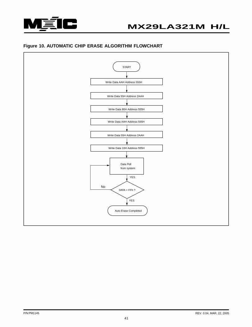
41
P/N:PM1145 REV. 0.04, MAR. 22, 2005
MX29LA321M H/L
Figure 10. AUTOMATIC CHIP ERASE ALGORITHM FLOWCHART
START
Write Data AAH Address 555H
Write Data 55H Address 2AAH
Write Data AAH Address 555H
Write Data 80H Address 555H
YES
Write Data 10H Address 555H
Write Data 55H Address 2AAH
DATA = FFh ?
YES
Auto Erase Completed
Data Poll
from system
No

42
P/N:PM1145 REV. 0.04, MAR. 22, 2005
MX29LA321M H/L
Figure 11. AUTOMATIC SECTOR ERASE ALGORITHM FLOWCHART
START
Write Data AAH Address 555H
Write Data 55H Address 2AAH
Write Data AAH Address 555H
Write Data 80H Address 555H
Write Data 30H Sector Address
Write Data 55H Address 2AAH
Auto Sector Erase Completed
Data Poll from System
YES
NOData=FFh?
Last Sector
to Erase ?
NO
YES

43
P/N:PM1145 REV. 0.04, MAR. 22, 2005
MX29LA321M H/L
Figure 12. ERASE SUSPEND/RESUME FLOWCHART
START
Write Data B0H
Toggle Bit checking Q6
not toggled
ERASE SUSPEND
YES
NO
Write Data 30H
Continue Erase
Reading or
Programming End
Read Array or
Program
Another
Erase Suspend ?NO
YES
YES
NO
ERASE RESUME

44
P/N:PM1145 REV. 0.04, MAR. 22, 2005
MX29LA321M H/L
AC CHARACTERISTICS
Alternate CE# Controlled Erase and Program Operations
Parameter Speed Options
Std. Description 70R 90 Unit
tWC Write Cycle Time (Note 1) Min 70 90 ns
tAS Address Setup Time Min 0 ns
tAH Address Hold Time Min 45 ns
tDS Data Setup Time Min 35 ns
tDH Data Hold Time Min 0 ns
tGHEL Read Recovery Time Before Write Min 0 ns
(OE# High to WE# Low)
tWS WE# Setup Time Min 0 ns
tWH WE# Hold Time Min 0 ns
tCP CE# Pulse Width Min 35 ns
tCPH CE# Pulse Width High Min 25 ns
Write Buffer Program Operation (Notes 2,3) Typ 240 us
Single Word/Byte Program Byte Typ 60 us
tWHWH1 Operation (Notes 2,5) Word Typ 60 us
Accelerated Single Word/Byte Byte Typ 54 us
Programming Operation (Notes 2,5) Word Typ 54 us
tWHWH2 Sector Erase Operation (Note 2) Typ 0.5 sec
tRH RESET HIGH Time Before Write (Note 1) Min 50 ns
tPOLL Program Valid Before Status Polling (Note 6) Max 4 us
Notes:1. Not 100% tested.2. See the "Erase And Programming Performance" section for more information.3. For 1-16 words/1-32 bytes programmed.4. Effective write buffer specification is based upon a 16-word/32-byte write buffer operation.5. Word/Byte programming specification is based upon a single word/byte programming operation not utilizing the write
buffer.6. When using the program suspend/resume feature, if the suspend command is issued within tPOLL, tPOLL must be
fully re-applied upon resuming the programming operation. If the suspend command is issued after tPOLL, tPOLL isnot required again prior to reading the status bits upon resuming.
TA=-40°°°°° C to 85°°°°° C, VCC=2.7V~3.6V (TA=0°°°°° C to 70°°°°° C, VCC=3.0V~3.6V for 70R)

45
P/N:PM1145 REV. 0.04, MAR. 22, 2005
MX29LA321M H/L
Figure 13. CE# CONTROLLED PROGRAM TIMING WAVEFORM
tWC
tWH
tGHEL
tWHWH1 or 2
tCP
Address
WE#
OE#
CE#
DataQ7
PA
Data# Polling
DOUT
RESET#
RY/BY#
NOTES:
1.PA=Program Address, PD=Program Data, DOUT=Data Out, Q7=complement of data written to device.2.Figure indicates the last two bus cycles of the command sequence.
tAH
tAS
PA for programSA for sector erase555 for chip erase
tRH
tDH
tDStWS
A0 for program55 for erase
tCPH
tBUSY
PD for program30 for sector erase10 for chip erase
555 for program2AA for erase

46
P/N:PM1145 REV. 0.04, MAR. 22, 2005
MX29LA321M H/L
SECTOR GROUP PROTECT/CHIP UNPROTECT
Figure 14. Sector Group Protect / Chip Unprotect Waveform (RESET# Control)
Note: For sector group protect A7=0, A2=1, A1=0. For chip unprotect A7=1, A2=1, A1=0
Sector Group Protect:150us
Chip Unprotect:15ms1us
VID
VIH
Data
SA, A7A2, A1
CE#
WE#
OE#
Valid* Valid*
Status
Valid*
Sector Group Protect or Chip Unprotect
40h60h60h
Verify
RESET#

47
P/N:PM1145 REV. 0.04, MAR. 22, 2005
MX29LA321M H/L
Figure 15. IN-SYSTEM SECTOR GROUP PROTECT/CHIP UNPROTECT ALGORITHMS WITH RESET#=VID
START
PLSCNT=1
RESET#=VID
Wait 1us
Set up sector address
Sector Protect:Write 60h to sector
address withA7=0, A2=1, A1=0
Wait 150us
Verify Sector Protect:Write 40h to sector
address withA7=0, A2=1, A1=0
Read fromsector address
withA7=0, A2=1, A1=0
Reset PLSCNT=1
Remove VID from RESET#
Write reset command
Sector ProtectAlgorithm
Chip UnprotectAlgorithmSector Protect complete
Remove VID from RESET#
Write reset command
Sector Unprotect complete
Device failed
Temporary SectorUnprotect Mode
Increment PLSCNT
Increment PLSCNT
First Write
Cycle=60h?
Set up first sector address
Protect all sectors:The indicated portion of
the sector protect algorithmmust be performed
for all unprotected sectorsprior to issuing the first
sector unprotect address
Sector Unprotect:Write 60h to sector
address withA7=1, A2=1, A1=0
Wait 15 ms
Verify Sector Unprotect:Write 40h to sector
address withA7=1, A2=1, A1=0
Read fromsector address
withA7=1, A2=1, A1=0
Data=01h?PLSCNT=25?
Device failed
START
PLSCNT=1
RESET#=VID
Wait 1us
First Write
Cycle=60h?
All sectors
protected?
Data=00h?PLSCNT=1000?
Last sector
verified?
Yes
YesYes
No
No
No
Yes
Yes
Yes
YesYes
Yes
No
No
No
No
No
No
Protect another
sector?
Reset PLSCNT=1
Temporary SectorUnprotect Mode

48
P/N:PM1145 REV. 0.04, MAR. 22, 2005
MX29LA321M H/L
Figure 16. SECTOR GROUP PROTECT TIMING WAVEFORM (A10, OE# Control)
Parameter Description Test Setup All Speed Options Unit
tVLHT Voltage transition time Min. 4 us
tWPP1 Write pulse width for sector group protect Min. 100 ns
tOESP OE# setup time to WE# active Min. 4 us
AC CHARACTERISTICS
tOE
Data
OE#
WE#
12V 3V
12V 3V
CE#
A10
A2
A7
tOESP
tWPP 1
tVLHT
tVLHT
tVLHT
Verify
01H F0H
A21-A17 Sector Address

49
P/N:PM1145 REV. 0.04, MAR. 22, 2005
MX29LA321M H/L
Figure 17. SECTOR GROUP PROTECTION ALGORITHM (A10, OE# Control)
START
Set Up Sector Addr
PLSCNT=1
Sector Protection
Complete
Data=01H?
Yes
OE#=VID, A10=VID, CE#=VIL
A7=VIL
Activate WE# Pulse
Time Out 150us
Set WE#=VIH, CE#=OE#=VIL
A10 should remain VID
Read from Sector
Addr=SA, A2=1
Protect Another
Sector?
Remove VID from A10
Write Reset Command
Device Failed
PLSCNT=32?
Yes
No
No
50
P/N:PM1145 REV. 0.04, MAR. 22, 2005
MX29LA321M H/L
Figure 18. CHIP UNPROTECT TIMING WAVEFORM (A10, OE# Control)
tOE
Data
OE#
WE#
12V 3V
12V 3V
CE#
A10
A2
tOESP
tWPP 2
tVLHT
tVLHT
tVLHT
Verify
00H
A7
F0H

51
P/N:PM1145 REV. 0.04, MAR. 22, 2005
MX29LA321M H/L
Figure 19. CHIP UNPROTECT FLOWCHART (A10, OE# Control)
START
Protect All Sectors
PLSCNT=1
Chip Unprotect
Complete
Data=00H?
Yes
Set OE#=A10=VID
CE#=VIL, A7=1
Activate WE# Pulse
Time Out 15ms
Set OE#=CE#=VIL
A10=VID, A2=1
Set Up First Sector Addr
All sectors have
been verified?
Remove VID from A10
Write Reset Command
Device Failed
PLSCNT=1000?
No
Increment
PLSCNT
No
Read Data from Device
Yes
Yes
No
Increment
Sector Addr
* It is recommended before unprotect whole chip, all sectors should be protected in advance.

52
P/N:PM1145 REV. 0.04, MAR. 22, 2005
MX29LA321M H/L
Figure 20. TEMPORARY SECTOR GROUP UNPROTECT WAVEFORMS
AC CHARACTERISTICS
Parameter Description Test All Speed Options Unit
Setup
tVIDR VID Rise and Fall Time (see Note) Min 500 ns
tRSP RESET# Setup Time for Temporary Sector Unprotect Min 4 us
tRRB RESET# Hold Time from RY/BY# High for Temporary Min 4 us
Sector Group Unprotect
RESET#
CE#
WE#
RY/BY#
tVIDR
12V
0 or 3V VIL or VIH
tRSP
tVIDR
Program or Erase Command Sequence
tRRB

53
P/N:PM1145 REV. 0.04, MAR. 22, 2005
MX29LA321M H/L
Figure 21. TEMPORARY SECTOR GROUP UNPROTECT FLOWCHART
Start
RESET# = VID (Note 1)
Perform Erase or Program Operation
RESET# = VIH
Temporary Sector Unprotect Completed(Note 2)
Operation Completed
2. All previously protected sectors are protected again.
Notes : 1. All protected sectors are temporary unprotected. VID=11.5V~12.5V
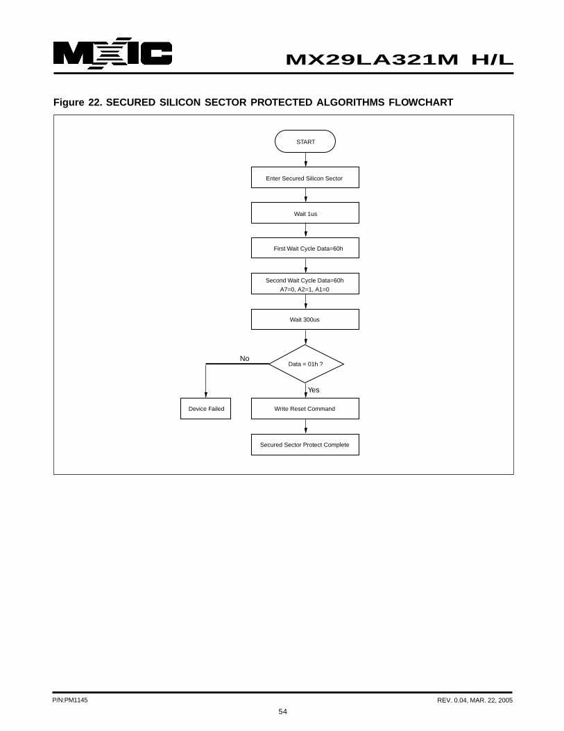
54
P/N:PM1145 REV. 0.04, MAR. 22, 2005
MX29LA321M H/L
Figure 22. SECURED SILICON SECTOR PROTECTED ALGORITHMS FLOWCHART
START
Enter Secured Silicon Sector
Data = 01h ?No
Yes
Wait 1us
First Wait Cycle Data=60h
Second Wait Cycle Data=60h
A7=0, A2=1, A1=0
Wait 300us
Write Reset CommandDevice Failed
Secured Sector Protect Complete

55
P/N:PM1145 REV. 0.04, MAR. 22, 2005
MX29LA321M H/L
Figure 23. SILICON ID READ TIMING WAVEFORM
tACC
tCE
tACC
tOE
tOH tOH
tDF
DATA OUT
Manufacturer ID Device IDCycle 1
Device IDCycle 2
Device IDCycle 3
VID
VIH
VIL
ADD
A10
ADD
CE#
A2
OE#
WE#
ADD
A1
DATA OUT DATA OUT DATA OUTDATAQ0-Q15
VCC3V
VIH
VIL
VIH
VIL
VIH
VIL
A3VIH
VIL
VIH
VIL
VIH
VIL
VIH
VIL
VIH
VIL
tACC tACC
tOH tOH

56
P/N:PM1145 REV. 0.04, MAR. 22, 2005
MX29LA321M H/L
WRITE OPERATION STATUS
Figure 24. DATA# POLLING TIMING WAVEFORMS (DURING AUTOMATIC ALGORITHMS)
Note :
VA=Valid address. Figure shows are first status cycle after command sequence, last status read cycle, and array data raed cycle.
tDF
tCE
tCH
tOE
tOEH
tACC
tRC
tOH
Address
CE#
OE#
WE#
Q7
Q0-Q6
RY/BY#
tBUSY
Status Data Status Data
Status Data Complement True Valid Data
VAVAVA
High Z
High ZValid DataTrue

57
P/N:PM1145 REV. 0.04, MAR. 22, 2005
MX29LA321M H/L
Figure 25. DATA# POLLING ALGORITHM
Notes:1.VA=valid address for programming.2.Q7 should be rechecked even Q5="1" because Q7 may change simultaneously with Q5.
Read Q7~Q0Add.=VA(1)
Read Q7~Q0Add.=VA
Start
Q7 = Data ?
Q5 = 1 ?
Q7 = Data ?
FAIL Pass
No
No
(2)
No
Yes
Yes
Yes
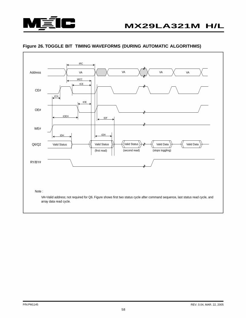
58
P/N:PM1145 REV. 0.04, MAR. 22, 2005
MX29LA321M H/L
Figure 26. TOGGLE BIT TIMING WAVEFORMS (DURING AUTOMATIC ALGORITHMS)
Note :
VA=Valid address; not required for Q6. Figure shows first two status cycle after command sequence, last status read cycle, and array data read cycle.
tDF
tCE
tCH
tOE
tOEH
tACC
tRC
tOH
Address
CE#
OE#
WE#
Q6/Q2
RY/BY#
tDH
Valid StatusValid Status
(first read)
Valid Status
(second read) (stops toggling)
Valid Data
VA VAVAVA
Valid Data

59
P/N:PM1145 REV. 0.04, MAR. 22, 2005
MX29LA321M H/L
START
Read Q7~Q0
Read Q7~Q0
YES
NOToggle Bit Q6
=Toggle?
Q5=1?
YES
NO
(Note 1)
Read Q7~Q0 Twice (Note 1,2)
Toggle Bit Q6=
Toggle?
Program/Erase Operation Not
Complete, Write Reset Command
YES
Program/Erase Operation Complete
Figure 27. TOGGLE BIT ALGORITHM
Notes :1. Read toggle bit twice to determine whether or not it is toggling.2. Recheck toggle bit because it may stop toggling as Q5 changes to "1".

60
P/N:PM1145 REV. 0.04, MAR. 22, 2005
MX29LA321M H/L
Figure 28. Q6 versus Q2
Note :
The system can use OE# or CE# to toggle Q2/Q6, Q2 toggles only when read at an address within an erase-suspended
WE#
Enter EmbeddedErasing
EraseSuspend
Enter EraseSuspend Program
EraseSuspendProgram
Erase SuspendRead
Erase SuspendRead
Erase
EraseResume
EraseComplete
Erase
Q6
Q2

61
P/N:PM1145 REV. 0.04, MAR. 22, 2005
MX29LA321M H/L
MIN. MAX.
Input Voltage with respect to GND on all pins except I/O pins -1.0V 13.5V
Input Voltage with respect to GND on all I/O pins -1.0V VCC + 1.0V
Current -100mA +100mA
Includes all pins except VCC. Test conditions: VCC = 3.0V, one pin at a time.
LATCH-UP CHARACTERISTICS
ERASE AND PROGRAMMING PERFORMANCE (1)
Notes:1. Typical program and erase times assume the following conditions: 25° C, 3.0V VCC. Programming specifications
assume checkboard data pattern.2. Maximum values are measured at VCC = 3.0 V, worst case temperature. Maximum values are valid up to and
including 100,000 program/erase cycles.3. Word/Byte programming specification is based upon a single word/byte programming operation not utilizing the
write buffer.4. For 1-16 words or 1-32 bytes programmed in a single write buffer programming operation.5. Effective write buffer specification is calculated on a per-word/per-byte basis for a 16-word/32-byte write buffer
operation.6. In the pre-programming step of the Embedded Erase algorithm, all bits are programmed to 00h before erasure.7. System-level overhead is the time required to execute the command sequence(s) for the program command. See
Table 3 for further information on command definitions.8. The device has a minimum erase and program cycle endurance of 100,000 cycles.
PARAMETER Typ (Note 1) Max (Note 2) Unit
Sector Erase Time 0.5 2 sec
Chip Erase Time 32 64 sec
Total Write Buffer Program Time (Note 4) 240 us
Total Accelerated Effective Write Buffer 200 us
Program Time (Note 4)
Chip Program Time 31.5 sec
Parameter Min Unit
Minimum Pattern Data Retention Time 20 Years
DATA RETENTION

62
P/N:PM1145 REV. 0.04, MAR. 22, 2005
MX29LA321M H/L
Parameter Symbol Parameter Description Test Set TYP MAX UNIT
CIN Input Capacitance VIN=0 TSOP 6 7.5 pF
CSP 4.2 5.0 pF
COUT Output Capacitance VOUT=0 TSOP 8.5 12 pF
CSP 5.4 6.5 pF
CIN2 Control Pin Capacitance VIN=0 TSOP 7.5 9 pF
CSP 3.9 4.7 pF
TSOP PIN AND BGA PACKAGE CAPACITANCE
Notes:1. Sampled, not 100% tested.2. Test conditions TA=25° C, f=1.0MHz

63
P/N:PM1145 REV. 0.04, MAR. 22, 2005
MX29LA321M H/L
ORDERING INFORMATION
PART NO. ACCESS TIME Ball Pitch/ PACKAGE Remark(ns) Ball size
MX29LA321MHTC-70R 70 56 Pin TSOP(Normal Type)
MX29LA321MHTC-90 90 56 Pin TSOP(Normal Type)
MX29LA321MLTC-70R 70 56 Pin TSOP(Normal Type)
MX29LA321MLTC-90 90 56 Pin TSOP(Normal Type)
MX29LA321MHTI-90 90 56 Pin TSOP(Normal Type)
MX29LA321MLTI-90 90 56 Pin TSOP(Normal Type)
MX29LA321MHTC-90G 90 56 Pin TSOP PB-free(Normal Type)
MX29LA321MLTC-90G 90 56 Pin TSOP PB-free(Normal Type)
MX29LA321MHTI-90G 90 56 Pin TSOP PB-free(Normal Type)
MX29LA321MLTI-90G 90 56 Pin TSOP PB-free(Normal Type)
MX29LA321MHXCC-70R 70 64 ball CSPMX29LA321MHXCC-90 90 64 ball CSPMX29LA321MLXCC-70R 70 64 ball CSPMX29LA321MLXCC-90 90 64 ball CSPMX29LA321MHXCI-70R 70 64 ball CSPMX29LA321MHXCI-90 90 64 ball CSPMX29LA321MLXCI-70R 70 64 ball CSPMX29LA321MLXCI-90 90 64 ball CSPMX29LA321MHXCC-90G 90 64 ball CSP PB-freeMX29LA321MLXCC-90G 90 64 ball CSP PB-freeMX29LA321MHXCI-90G 90 64 ball CSP PB-freeMX29LA321MLXCI-90G 90 64 ball CSP PB-free
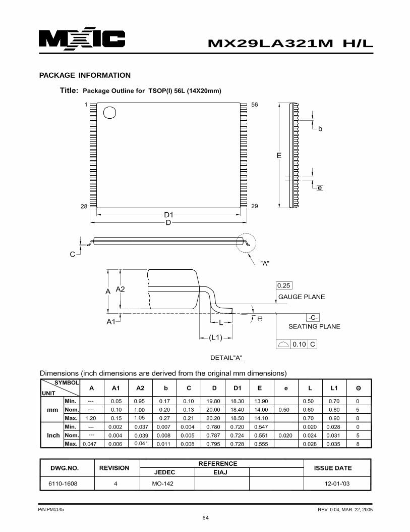
64
P/N:PM1145 REV. 0.04, MAR. 22, 2005
MX29LA321M H/L
PACKAGE INFORMATION

65
P/N:PM1145 REV. 0.04, MAR. 22, 2005
MX29LA321M H/L

66
P/N:PM1145 REV. 0.04, MAR. 22, 2005
MX29LA321M H/L
REVISION HISTORY
Revision No. Description Page Date0.01 1. To modified sector group address table P8 DEC/08/2004
2. To modified CFI parameter P23,243. To added TA=0° C to 70° C , VCC=3.0V~3.6V for 70R operation P30,32,35,44
0.02 1. Content errors All DEC/15/20040.03 1. To modified content description P1,2,9,11, DEC/24/2004
P18,610.04 1. Changed title from "Advanced Information" to "Preliminary" P1 MAR/22/2005

MX29LA321M H/L
MACRONIX INTERNATIONAL CO., LTD.Headquarters:TEL:+886-3-578-6688FAX:+886-3-563-2888
Europe Office :TEL:+32-2-456-8020
FAX:+32-2-456-8021
Hong Kong Office :TEL:+86-755-834-335-79FAX:+86-755-834-380-78
Japan Office :Kawasaki Office :TEL:+81-44-246-9100
FAX:+81-44-246-9105Osaka Office :TEL:+81-6-4807-5460
FAX:+81-6-4807-5461
Singapore Office :TEL:+65-6346-5505FAX:+65-6348-8096
Taipei Office :TEL:+886-2-2509-3300FAX:+886-2-2509-2200
MACRONIX AMERICA, INC.TEL:+1-408-262-8887
FAX:+1-408-262-8810
http : //www.macronix.com
MACRONIX INTERNATIONAL CO., LTD. reserves the right to change product and specifications without notice.