myoelectric signal monitoring system -...
TRANSCRIPT

Myoelectric Signal
Monitoring System
Fabiano Reis Mendes
Departamento de Engenharia Electrotécnica
Mestrado em Engenharia Electrotécnica e de Computadores
Área de Especialização em Automação e Sistemas
2015

This report satisfies partially the requirements to the subject of Thesis / Dissertation of
Electrical and Computer Engineer MSc.
Candidate: Fabiano Reis Mendes, nº 1091170, [email protected]
Supervisor: José Alberto Machado da Silva, [email protected]
Co-supervisor: Gustavo Alves, [email protected]
Departamento de Engenharia Electrotécnica
Mestrado em Engenharia Electrotécnica e de Computadores
Área de Especialização em Automação e Sistemas
2015

In memory of
Mário de Almeida Mendes

i
Acknowledgments
I would like to thank everybody who helped me along the development of this work. In
particular, I am grateful to:
- whom made it possible for me to come and stay in Portugal: my parents Doralice and
Joaquim, my uncle Mário, my aunt Isabel, my brother Mário and my sister Izabel, my
cousin Doris and her husband Francisco, the marital Flávia and Leonardo;
- friends from the laboratory: Eng. Helder, Eng. João, Eng. Nuno, Eng. João Loureiro, Eng.
Ruben;
- all friends that provided help in any way: Fernando, Carlos and the marital Paulo and
Angelúzia;
- professor João Canas Ferreira for providing the microprocessor development kit;
- professors Machado da Silva and Gustavo Alves for their receptiveness, availability and
patience.
Thank you all.


iii
Abstract
The Electromyography (EMG) is an important tool for gait analyzes and disorders
diagnoses. Traditional methods involve equipment that can disturb the analyses, being
gradually substituted by different approaches, like wearable and wireless systems. The
cable replacement for autonomous systems demands for technologies capable of
meeting the power constraints. This work presents the development of an EMG and
kinematic data capture wireless module, designed taking into account power
consumption issues.
This module captures and converts the analog myoeletric signal to digital, synchronously
with the capture of kinetic information. Both data are time multiplexed and sent to a PC
via Bluetooth link. The work carried out comprised the development of the hardware, the
firmware and a graphical interface running in an external PC. The hardware was
developed using the PIC18F14K22, a low power family of microcontrollers. The link was
established via Bluetooth, a protocol designed for low power communication. An
application was also developed to recover and trace the signal to a Graphic User Interface
(GUI), coordinating the message exchange with the firmware. Results were obtained
which allowed validating the conceived system in static and with the subject performing
short movements. Although it was not possible to perform the tests within more dynamic
movements, it is shown that it is possible to capture, transmit and display the captured
data as expected. Some suggestions to improve the system performance also were made.
Keywords:
Electromyography, microcontroller, Bluetooth, low power.


v
Resumo
A eletromiografia constitui uma importante ferramenta de diagnóstico na avaliação de
patologias relacionadas à marcha. Os métodos tradicionais usam equipamento que pode
prejudicar a análise e que vem gradualmente sendo substituído por sistemas sem fios e
que proporcionam melhor conforto durante a análise. A substituição de sistemas com
cablagem por sistemas autónomos requer o uso de tecnologias voltadas para o baixo
consumo de energia. Este trabalho tem por objetivo apresentar uma solução alternativa
de captura e transmissão de dados sem fios, desenvolvida tendo em consideração
questões de consumo e portabilidade, recorrendo as soluções disponibilizadas no mercado
com base no uso de microprocessadores.
O sistema projetado tem como função converter o sinal mioelétrico de analógico para
digital, multiplexá-lo com os dados cinéticos e enviá-los para um terminal remoto. O
trabalho consiste no desenvolvimento do Hardware, do Firmware e de uma interface
gráfica. Para o desenvolvimento do Hardware foi usado o PIC18F14K22, que pertence a
família de microcontroladores de baixo consumo. O Bluetooth, que é um protocolo de
comunicação desenvolvido para aplicações de baixo consumo, foi usado para o
estabelecimento do enlace. A aplicação desenvolvida tem a função de recuperar os dados
e exibí-los em uma interface gráfica, além de coordenar a troca de mensagens com o
Firmware. Embora não tenha sido possível executar os testes dinamicamente, mostra-se
com os testes realizados em regime estático ou com movimentos curtos, que os dados
foram capturados, transmitidos e reproduzidos de forma fidedigna e de acordo com o
esperado. Finalmente são feitas algumas sugestões que podem melhorar o desempenho
do sistema projetado.
Palavras chaves:
Eletromiografia, microcontrolador, Bluetooth, baixo consumo.


vii
Table of Contents
1. Introduction ...........................................................................................................................1
1.1. Context ..........................................................................................................................4
1.2. Objective ........................................................................................................................4
1.3. Organization of the Dissertation .....................................................................................5
1.4. Scheduling ......................................................................................................................6
2. Human Gait Analysis and the Characteristics of Myoeletric Signals ................................................7
2.1. Human Gait ....................................................................................................................7
2.1.1. Kinetic analyses. ......................................................................................................8
2.1.2. Muscular activity during gait. ..................................................................................9
2.2. The Myoeletric Signal ................................................................................................... 11
2.3. Noise Sources ............................................................................................................... 13
2.4. Signal Conditioning and Input Stage .............................................................................. 14
2.5. Myoeletric Sensors ....................................................................................................... 15
2.6. Mathematical Treatment .............................................................................................. 18
2.7. Measuring the Velocity ................................................................................................. 19
2.8. Conclusion .................................................................................................................... 19
3. Technologies ........................................................................................................................ 21
3.1. Network Topologies ...................................................................................................... 24
3.2. Network Configuration ................................................................................................. 26
3.3. Wireless Link and Protocols .......................................................................................... 27
3.4. Bluetooth Architecture ................................................................................................. 30
3.5. Bluetooth Operation ..................................................................................................... 32
3.6. The Bluetooth Module RN41......................................................................................... 34
3.7. The Processor ............................................................................................................... 34
3.8. The PIC18F14K22 .......................................................................................................... 35
3.9. Sensing Devices and Interface ....................................................................................... 36
4. The Design of the System ..................................................................................................... 39
4.1. The Hardware ............................................................................................................... 39
4.1.1. The PIC18F14K22 Characteristics........................................................................... 40

viii
4.1.2. The Accelerometer Electrical Characteristics ......................................................... 41
4.1.3. The RN41 Characteristics ...................................................................................... 43
4.1.4. EMG Conditioning Module .................................................................................... 44
4.1.5. SPI Interface.......................................................................................................... 45
4.1.6. USART Interface .................................................................................................... 47
4.1.7. In-Circuit Serial Programming (ICSPTM) .................................................................. 48
4.2. The Final Hardware ....................................................................................................... 49
4.3. Bluetooth Module Configuration .................................................................................. 50
4.4. The MCU Programming and Configuration .................................................................... 51
4.5. The Firmware ............................................................................................................... 57
4.5.1. The Packages Formation ....................................................................................... 59
4.5.2. System Requirements ........................................................................................... 60
4.5.3. Firmware Algorithm .............................................................................................. 62
4.6. The Software ................................................................................................................ 64
5. Tests and Validations............................................................................................................ 67
5.1. Module Bluetooth - MCU Communication .................................................................... 67
5.2. Sampling Test ............................................................................................................... 67
5.3. Accelerometer – MCU SPI Communication ................................................................... 70
5.4. Test to the Final System ................................................................................................ 71
5.5. Functional Testing ........................................................................................................ 72
5.6. Evaluation of the Power Consumption .......................................................................... 76
6. Conclusions .......................................................................................................................... 79
Bibliography ................................................................................................................................. 83
Annex A – Calculations ................................................................................................................. 87
Annex B - Schematic..................................................................................................................... 99
Annex C – Programming Codes .................................................................................................. 101

ix
List of Figures
Figure 1 – Planned workflow. .........................................................................................................6 Figure 2 - The reference planes of the human body in the standard anatomical position. [9] This figure was edited to add the Cartesian reference. ..........................................................................8 Figure 3 - “Division of normal gait cycle (illustration of right leg). Numbers indicate percent of gait cycle.” [11] .............................................................................................................................9 Figure 4 - Expected muscle activation of major lower limb muscles in function of the gait. [9] .... 10 Figure 5 - Major lower limb muscle identification [12]. ................................................................. 10 Figure 6 - “Schematic representation of the generation of the MUAP.” [13] ................................. 11 Figure 7 - “The raw EMG recording of 3 contractions bursts of the M. biceps br.” [14] ................. 12 Figure 8 - Examples of 200 ms of simulated EMG signals with different distortions[18]. ............... 13 Figure 9 - “A simple biopotential amplifier design based on an integrated-circuit instrumentation amplifier” [4]. .............................................................................................................................. 15 Figure 10 – Representation of main types of electrodes used in EMG. (a) respectively: the monopolar needle, the multipolar needle and the concentric needle [16]. (b) surface electrode and its cut view [15]. The bipolar and monopolar configuration of this electrode is represented in (c) and (d) respectively. (e) represents a surface electrode grid [15] and (f) represents a surface electrode array [15]. .................................................................................................................... 17 Figure 11 – Measurement of speed of signal propagation by row surface EMG. [20] .................... 19 Figure 12 - The main components of common WSN nodes. .......................................................... 21 Figure 13 - Basic network topologies: (a) Point-to-point, (b) Star, (c) Mesh, (d) Star-Mesh hybrid, (e) Cluster tree. [7] ....................................................................................................................... 24 Figure 14 - “Star vs. mesh-based body sensor network.”[7] .......................................................... 25 Figure 15 – WSN and the participants. The node is composed by CU that acts like a bridge. ......... 26 Figure 16 – “Comparison of the power consumption for each protocol.” [23] .............................. 29 Figure 17 – “Comparison of the normalized energy consumption for each protocol.”[23] ............ 29 Figure 18 - The Bluetooth protocol stack. [25] .............................................................................. 31 Figure 19 - “Bluetooth connection setup” [7] ............................................................................... 33 Figure 20 – Top and bottom view of electrodes used in EMG. ...................................................... 37 Figure 21 – Block diagram to the intended hardware system. ...................................................... 39 Figure 22 – PIC18F14K22 pinouts [27]. ......................................................................................... 40 Figure 23 – SCA3000-D01 embedded on a PWB and its pinout. .................................................... 43 Figure 24 – The Bluetooth module RN41 on bottom view (a) and on top view (b). [30] ................ 43 Figure 25 – EMG conditioning module (a) top view (b) bottom view............................................. 45 Figure 26 – SPI configuration for multiple slaves. The MISO, MOSI and CLK signal are available on a bus............................................................................................................................................... 46 Figure 27 – SPI line operations [28]. ............................................................................................. 47 Figure 28 – ICSP circuit interface and isolation circuitry [32]. ........................................................ 49 Figure 29 – Hardware assembly. .................................................................................................. 50 Figure 30 – Tasks performed in the two states of the main code. ................................................. 57 Figure 31 – Handshake diagram between the remote system and the user interface. .................. 58 Figure 32 – The firmware block diagram....................................................................................... 59 Figure 33 – Packet format and frame sequence. ........................................................................... 60 Figure 34 – Form window application fashion. ............................................................................. 64 Figure 35 – Sinusoidal signal with frequency of 100 Hz recovered. ............................................... 68 Figure 36 – Triangular signal with frequency 100 Hz recovered. ................................................... 68 Figure 37 - Sinusoidal signal with frequency of 1 kHz recovered. .................................................. 69 Figure 38 - Triangular signal with frequency of 1 kHz recovered. .................................................. 69

x
Figure 39 – The waveform obtained from the test to the complete system, displayed on the developed GUI: (a) shows the sinusoidal wave from signal generator; (b) is an unused input meant to the accelerometer data; (c) shows a 2nd input with three axes accelerometer data. ................. 71 Figure 40 – Sinusoidal recovered signal expanded. ....................................................................... 72 Figure 41 – EMG signal and acceleration shown in the GUI: (a) shows a raw EMG in some isometric contractions performance; (b) shows the EMG smoothened with a 50 s RMS time window; (c) shows the three axes acceleration data........................................................................................ 73 Figure 42 – EMG outline for 500 s RMS time window. .................................................................. 73 Figure 43 – Signal expanded on the time scale: (a) is a raw EMG contraction; (b) shows the contraction smoothened; (c) shows the acceleration data. .......................................................... 74 Figure 44 – EMG signal at the second channel and the acceleration chart: (a) shows a raw EMG in some isometric contraction; (b) shows the EMG smoothened with a 500 s RMS time window; (c) shows the three axes acceleration data........................................................................................ 74 Figure 45 – Time expanded EMG signal for the second channel. ................................................... 75 Figure 46 – EMG waveform and acceleration obtained from a similar system. [36] ...................... 75 Figure 47 – Waveform of the power supply voltage obtained from a digital scope. ...................... 76

xi
List of Tables
Table 1 – Dynamic Voltage Range for some EMG application. This table was edited from the original [17]. ................................................................................................................................ 12 Table 2 – “Recommended Bandwidth for EMG Amplifiers” [15]. .................................................. 16 Table 3 – Most notorious WSN node platform with their features. [21]. ....................................... 23 Table 4 - Comparison of the Bluetooth, UWB, ZigBee, and Wi-Fi protocols [23] ............................ 28 Table 5 – Main features and electrical characteristic of PIC18F14K22. .......................................... 40 Table 6 - PIC18F14K22 pin summary. ........................................................................................... 41 Table 7 – SCA3000-D01 electrical characteristic [29] [28]. ............................................................ 42 Table 8 – Accelerometer PWB pinout. .......................................................................................... 42 Table 9 – RN41 socket module pinout. ......................................................................................... 43 Table 10 – RN41 electrical characteristic [26]. .............................................................................. 44 Table 11 – Average power consumption regarding the operation mode [26]. ............................... 44 Table 12 – I/O reference to the EMG conditioning module. .......................................................... 45 Table 13 – Recommended resistor value for stable operation. ..................................................... 46 Table 14 – Registers addresses for read operation to SCA3000-D01. ............................................ 47 Table 15 – SPI standard bus modes. ............................................................................................. 54 Table 16 – Value for k in function of the EUSART operation mode. ............................................... 55 Table 17 – Acceleration value measured for each axis in the vertical position. ............................. 70 Table 18 – System power consumption at idle and contribution from each component. .............. 77 Table 19 - System power consumption at run mode and contribution from each component. ..... 77


xiii
Acronyms and Abbreviations
ACC - Accelerometer
ACL - Asynchronous Connectionless
AD - Analog – Digital
ADC - Analog – Digital Converter
AFE - Analog Front End
API - Application Programming Interface
ASIC - Application Specific Integrated Circuit
BAN - Body Area Network
BRG - Baud Rate Generator
BSN - Body Sensor Network
BT-LE - Bluetooth Low Energy
Bth - Bluetooth
Ckt - Circuit
CMRR - Common-Mode Rejection Ratio
CPU - Central Processing Unit
CTP - Cordless Telephony Profile
CU - Central Unit
DA - Digital – Analog
DAC - Digital – Analog Converter
DC - Direct Current
DLS - Double Limb Support stage
DNP - Dial-up Networking Profile
DSC - Digital Signal Controller
DSP - Digital Signal Processor
EEPROM - Electrically Erasable Programmable Read-Only Memory
ECCP - Enhanced Capture / Compare / Pulse Width Modulation
ECG - Electrocardiography
EDR - Enhanced Data Rate
EEG - Electroencephalography
EMG - Electromyography
EUSART - Enhanced Universal Synchronous - Asynchronous Receiver – Transmitter
FEC - Forward Error Correction
FFT - Fast Fourier Transforming
FIFO - First Input – First Output

xiv
FP - Fax Profile
FTP - File Transfer Profile
GAP - Generic Access Profile
GOEP - Generic Object Exchange Profile
GUI - Graphic User Interface
HCI - Host Controller Interface
HS - Headset
I²C - Integrated Interconnect
I/O - Input / Output
ICSP - In-Circuit Serial Programming
IDE - Integrated Development Environment
IEEE - Institute of Electrical and Electronics Engineers, Inc
IP - Intercom Profile1
IP - Internet Protocol1
IrMC - Infrared Mobile Communication
ISM - Industrial, Scientific and Medical
L2CAP - Logical Link and Control Adaptation Protocol
LAN - Local Area Network
LAP - Local Area Network Profile
LED - Light Emission Diode
LMP - Link Manager Protocol
LSb - Least Significant bit
LSB - Least Significant Byte
MAC - Medium Access Control layer
MBAN - Medical Body-Area Networks
MCU - Microcontroller Unit
MISO - Master Input Slave Output
MOSI - Master Output Slave Input
MIP - Million Instructions per Second
MSb - Most Significant bit
MSB - Most Significant Byte
MSSP - Master Synchronous Serial Port
MU - Motor Unit
MUAPT - Motor Unit Action Potential
NRZ - Non-Return-to-Zero
OBEX - Object Exchange Protocol
1 These two acronyms are identical; however they are both standard and able to be distinguished, according
to the context.

xv
OPAMP(s) - Operational Amplifier(s)
OS - Operating System
OSI - Open System Interconnection
P2P - Peer-to-Peer
PC - Personal Computer
PCB - Printed Circuit Board
PHY - Physical layer
PLL - Phase Lock Loop
PPP - Point-to-Point Protocol
PSD - Power Spectrum Density
PWB - Printed Wire Board
PWM - Pulse Width Modulation
R/W - Read and Write
RAM - Random Access Memory
RCU - Recording Central Unit
RF - Radiofrequency
RFCOMM - Radio frequency communication protocol
RISC - Reduced Instruction Set Computer
RMS - Root Mean Square
RX - Reception
SCI - Serial Communications Interface
SCO - Synchronous Connection-Oriented
SDAP - Service Discovery Application Profile
SDP - Service Discovery Protocol
SEMG - Surface Electromyography
SIG - Special Interest Group
SLS - Single Limb Support stage
SNR - Signal Noise Ratio
SP - Synchronization Profile
SPI - Serial Peripheral Interface
SPP - Serial Port Profile
TCS - Telephony Control Specifications
TCP - Transport Control Protocol
TX - Transmission
UART - Universal Asynchronous Receiver - Transmitter
UDP - User Datagram Protocol
UHF - Ultra High Frequency
USART - Universal Synchronous - Asynchronous Receiver - Transmitter
xvi
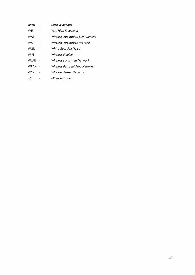
UWB - Ultra Wideband
VHF - Very High Frequency
WAE - Wireless Application Environment
WAP - Wireless Application Protocol
WGN - White Gaussian Noise
WiFi - Wireless Fidelity
WLAN - Wireless Local Area Network
WPAN - Wireless Personal Area Network
WSN - Wireless Sensor Network
µC - Microcontroller

1
1. INTRODUCTION
Myoeletric signals are the result of membrane depolarization during muscular activity
that generates a weak, but detectable electric field. Different concentrations of ions K+,
Ca++ and Na+ cause a difference of potential through muscular and nervous cell
membranes. The propagation of a stimulus occurs with a temporary altering of
concentration between inner and outer of cells environment. By its biological origin, the
myoeletric signal can be included into the set of biosignals that can provide information
about the physiological state [1].
The Electromyography is the act of recording the myoeletric signals through sensors and
display by a graphical interface. Analyses involving EMG are reported since 1849, when
surface electrodes sensors were used to capture the myoeletric signal from a muscle.
Thereafter, at 1929, a concentric needle was used that allowed to detect the signal from a
single Motor Unit2 (MU) [2]. These early studies were improved by enhancement of
techniques like noise filtering, signal processing, sensing; being widely used in many
fields, especially on medicine with clinical, research, rehabilitation and sportive purposes.
“Clinically EMG is used to determine the function of muscle groups following trauma. It
may also be used to assess muscle function following suspected neurological damage.” [1]
The association with mechanical sensors such as accelerometers or gyroscope is relatively
recent and most applied to upper limbs than to lower limb, in which the usage of cameras
and feet platforms is still predominant to kinesiological pattern analysis. The usage of
multichannel sensing it is necessary to generate a spatial and temporal representation of
a movement pattern and associate it to a muscle or to a muscular group activity [3].
Nowadays efforts have been focused on the development of nonintrusive techniques,
through innovative surface detection systems, that avoid complications inherent to the
invasive techniques. Some works have been conducted in this field leading to studies to
2 It is called Motor Unit a single nervous pathway that controls one or more muscular fiber(s).

2
develop wearable sensors clothes with the purpose of measuring the biosignal generated
by the body. These clothes have the promise to be used to diagnosis motor-neural illness
associated, although it represents more complex and expensive method [4] [5].
It is possible to identify three main conditions in which the Surface EMG (SEMG) is
commonly applied. The first one is done under static posture to evaluate a possible
impairment on a specific peripheral nerve. In this case the SEMG is used as a
complementary way to the intrusive EMG. The second is done in the same static
condition than the first one but directly applied over one whole nervous arc to assess a
potential neuromotor disorder along the stimulus-reflex response pathway. The third
condition is that the signal is recorded during an intentional motor action with the
purpose of evaluating cyclical movement patterns. If applied jointly with kinesiological
sensing it will be possible to relate a motion disturbance to an individual muscle [3].
The SMEG is limited to the more superficial and larger muscles because it is more liable to
the adjacent muscles interference when applied to smaller or deeper muscles, but is
more efficient to global analysis of movement [3]. The accuracy of intrusive EMG
evaluation is hindered by limitations of movements during a motor task, achieving thus,
the same conditions of accuracy than SEMG. Different membranes elasticity affects both
recording methods, with noise added by electrodes displacement from target on SEMG
and the discomfort caused by the needle on intrusive EMG. In this regard two techniques
have different indications [3].
On the analysis of human gait the SEMG is indicated because allows more movement
freedom, but in a complete analysis in which it is required kinetic and kinesiological data,
cables and increased amount of sensors can also affect the natural flow of gait and return
altered results. The replacement of cables by wireless connection is the traditional
solution. Some dedicated protocols have been proposed in some studies but the trend it
is the usage of standardized protocols, mainly the WiFi, the Bluetooth and the ZigBee.
Another possible solution is on standalone scenario, in which data is recorded to a card
memory. The size and the weight of the apparatus is a solved question with the devices
miniaturization. Portability, mobility, and comfort are issues to be thought to conceive
non-intrusive methods and thus, to get trust results [3].

3
In any choice for wireless communication it is necessary to consider the power supply to
ensure the device’s autonomy during a time enough to perform the desired evaluation.
The wireless component has been identified as a major power consumer in
programmable smart devices. These devices are supplied with batteries that must satisfy
the size and weight constrains for the portability [6].
The efforts to solve the supply issues, which are common to all electric and electronic
apparatus, are concentrated on three research branches: the energy density and storing,
energy source and energy saving. The first branch goes to increase chemically the power
density and the efficiency, like the addition of graphite, silicon or boron to lithium
batteries, being a field of engineer of materials. The second branch is concentrated in
manners to convert the energy using alternative sources to (re)charge and its reusing, for
example photovoltaic microcells, piezoelectric materials or biological heating. The third
branch focuses systems designed to save and manage the power consumption, at
semiconductor and programming levels. Some solutions are strongly present nowadays
although yet in maturing process to its consolidation, being objects of constants efforts to
improvements.
The most usual configuration of the EMG system uses a Central Unit (CU) based on
Microcontroller or on Digital Signal Processor (DSP) to collect and process data from
sensors. Several manufacturers provide devices that meet the EMG system constrains
what explain their widely acceptance. These devices are designed for minimum power
consumption and are flexible and versatile to allow operating with many standardized
communication protocols. Although can perform the role of data center recover the great
trend is the usage like a node, intermediating the EMG system to another remote point
that can be a Data Base, a Local Area Network (LAN), Internet or other device. The link is
made essentially by Bluetooth or ZigBee protocols, which are designed to establish
communication routines thought in minimum effort along link that allow more power
efficiency to implement a network than Wireless Fidelity (Wi-Fi).
The network architecture is other aspect that can be handled to improve the energy
efficiency affecting the sensors configuration and the data exchange. Sensor’s amount
and disposal can drain energy as autonomous as they are and as linked as they are to

4
others components. The simplicity of the network of sensors implies delegation of more
working to the Recording CU (RCU). The ideal topology is subject of studies that bring the
concept of Body Sensor Network (BSN) [7].
This issue becomes so important that The Institute of Electrical and Electronics
Engineers, Inc (IEEE) introduces the concept of Body Area Network (BAN) and since
2008 creates a task group to specify the standard 802.15/6TM, “(…) optimized for low
power devices and operation on, in or around the human body (but not limited to
humans)(…)” [8]. The BSN takes part in medical applications but the BAN predicts
other applications like “consumer electronics / personal entertainment (…)” [8]. More
generally, the standard 802.15TM cares every kind of Wireless Personal Area Network
(WPAN) that treats all kind off network nearby human body.
1.1. CONTEXT
ProLimb is a project developed at INESC Porto with the purpose of developing a ‘knit
of sensors’. The result was a wearable legging incorporating a system that is capable
of recording EMG signals of both legs during gait. The matching with a personal
interest in this area has motivated to present the theme of the thesis like a partial
requirement for the Master in Electronic Computer Engineering in branch Automation
and Systems (MEEC / AS) at Instituto Superior de Engenharia do Porto (ISEP).
1.2. OBJECTIVE
This work aimed at designing a portable low power system to capture the myoeletric
and mechanical signals through sensors and send them to a terminal computer, where
the waveform will be displayed. The first purpose of this system is the prophylaxis of
lower limb diseases after the extraction of relevant features of the signals. A
requirement is the usage of non intrusive techniques that suggests the usage of
surface electrodes to get myoeletric signals. The assessment is done during a
movement task, in which was chosen the human gait to be evaluated because it is the
most common and evident motor action.

5
To achieve this objective, the work was subdivided in some partial goals that started by
study of the signals to be monitored and also about the dynamic of the target movement.
It followed the implementation of sensors module meant to condition the captured
signals and the development of a central unit based on microprocessor to capture the
signals. This central unit has the purpose of multiplexing signals from different muscles
and sensors before sending them through the wireless link. It is proposed to establish the
wireless connection with a communication module, that the Bluetooth is suggested
because its widely usage and acceptance. A Personal Computer (PC) will receive,
demultiplex and display the data by an application, in which is suggested the deployment
of a user interface software. The developed system must be validated through tests and
reported.
1.3. ORGANIZATION OF THE DISSERTATION
Regarding the goals of the work, it is possible divide the tasks in some steps and present
them in six chapters:
In this first chapter is described how this report is organized, the workflow and the
organization of tasks as well its scheduling. A brief introduction about the theme exposing
the assumption and the aim of the work are also given.
At the second chapter the theme will be unfolded, highlighting important issues
necessary to understand the nature of signals and to get necessary expertise to develop
the work. Physiological and biomechanical aspects will be addressed to identify the
physical features that carry recoverable information. The sensing process is described to
understand how the noise inserted affects the system. Filters must be applied to remove
or reduce these noises and they will be mentioned in this topic too.
The third chapter makes a review in the used platforms, common architecture, the
topologies network and protocols. Communication options and protocols capable to
satisfy system conditions will be discussed. The proposed devices that will compose the
system and their features will be presented, giving a previewing of the system’s
architecture and its operation.

6
The fourth chapter is dedicated to the mounting and to the final conceiving of the system
in its two levels, hardware and software. The firmware to run in the hardware and the
graphical interface to run in the user terminal will take part in this chapter along with
their algorithms. The communication between points will obey some rules to ensure the
correct message exchange, in which will be clear by a handshaking scheme.
The fifth chapter brings the tests to be made onto the system and the results to be
obtained, with the purpose to evaluate and validate the system. The plotting of the
obtained waveform must be shown highlighting relevant characteristics to allow a user
identifying a possible disturbance.
The thesis is finalized with the sixth chapter, in which are discussed the obtained results
and the conclusions are shown. At this time may be enumerated the difficulties to
achieve the results and, based on them and on the conclusions, it is intended doing
suggestions to following studies and to improve the system.
1.4. SCHEDULING
Figure 1 – Planned workflow.
The process of development of the system can be divided into six main stages. Figure 1
depicts how these stages are divided and the presumptive relative time for their
execution. It begins with the system conceiving and the hardware implementation. With
initial hardware it is possible to start the firmware deployment. The link establishment
involves two parts, being the stage that follows the firmware deployment. When done, it
is allowed starting the first tests and their documentation. The final task is the report
written.
0 1 2 3 4 5 6 7
System concieving
Hardware assembling
Firmware deployment
Link Bth establishment
Tests to the System
Written

7
2. HUMAN GAIT ANALYSIS AND THE
CHARACTERISTICS OF MYOELETRIC SIGNALS
The SEMG is a powerful tool to record the neurophysiologic responsible for the
movement. The gait analysis involves the correlation between the generated signal and
the obtained kinesiological response. A possible pathology can be present when this
response does not correspond to an expected movement pattern or when an unexpected
behavior is seen in the myoeletric waveform. Amid to these procedures the signal must
be recorded and treated in order to delivery readable parameters for comparison.
Sensors are used to capture the electric stimulus which contains myoeletric information
and noise. Some different types of sensors are available with specific purpose and
response to the input signal. Before performing any analysis, the noise, which is
originated from several sources, must be extracted from the signal to turn it comparable
to electrical and kinetic standards parameters. In this regard, this section reviews theses
standards for the cyclical event analysis and waveform analysis before describe the
electrical characteristic and forms of to capture and treat the myoeletric signal.
2.1. HUMAN GAIT
The simple analyses of lower limb in human gait can be reduced to three main joints:
the hip, the knee and ankle. Theses joints are formed by four segments: the pelvis, the
thigh, the shank and the foot, and the angles between segments are used to compute
the kinematic data of gait [9]. The movement is done over three dimensional
Cartesians planes of these segments. Anatomically these planes are known as sagittal
plane, which crosses vertically the body on back-front direction and coincides with
plane xz (Figure 2); the frontal plane that crosses vertically the body side to side

8
direction, represented on yz Cartesian plane; and transverse plane, that crosses the body
horizontally, viewed in the Figure 2 on xy plane [10].
Figure 2 - The reference planes of the human body in the standard anatomical position. [9] This figure
was edited to add the Cartesian reference.
2.1.1. KINETIC ANALYSES.
The analysis of gait is made over each cycle in comparison with a standard gait cycle. One
cycle comprises one stride or two alternated steps. The moment of initial contact of one
limb with floor marks the beginning of the cycle and will be completed with the next
initial contact of the same limb with floor (Figure 3). Although the analysis over the tree
planes is relevant to describe the gait accurately, most of the analyses just assess the
movement over sagittal plane, which is regarded as the most important [10].
9
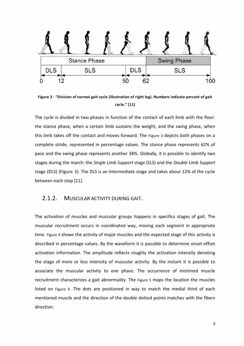
Figure 3 - “Division of normal gait cycle (illustration of right leg). Numbers indicate percent of gait
cycle.” [11]
The cycle is divided in two phases in function of the contact of each limb with the floor:
the stance phase, when a certain limb sustains the weight, and the swing phase, when
this limb takes off the contact and moves forward. The Figure 3 depicts both phases on a
complete stride, represented in percentage values. The stance phase represents 62% of
pace and the swing phase represents another 38%. Globally, it is possible to identify two
stages during the march: the Single Limb Support stage (SLS) and the Double Limb Support
stage (DLS) (Figure 3). The DLS is an intermediate stage and takes about 12% of the cycle
between each step [11].
2.1.2. MUSCULAR ACTIVITY DURING GAIT.
The activation of muscles and muscular groups happens in specifics stages of gait. The
muscular recruitment occurs in coordinated way, moving each segment in appropriate
time. Figure 4 shows the activity of major muscles and the expected stage of this activity is
described in percentage values. By the waveform it is possible to determine onset-offset
activation information. The amplitude reflects roughly the activation intensity denoting
the stage of more or less intensity of muscular activity. By the instant it is possible to
associate the muscular activity to one phase. The occurrence of mistimed muscle
recruitment characterizes a gait abnormality. The Figure 5 maps the location the muscles
listed on Figure 4. The dots are positioned in way to match the medial third of each
mentioned muscle and the direction of the double dotted points matches with the fibers
direction.

10
Figure 4 - Expected muscle activation of major lower limb muscles in function of the gait. [9]
Figure 5 - Major lower limb muscle identification [12].

11
2.2. THE MYOELETRIC SIGNAL
The stimulation of muscle fiber membrane is done in any point by a motoneuron,
commonly nearby at mid distance. The depolarization propagates in both directions along
the fiber to repolarize in the end. The complete electric phenomenon is known as action
potential and its duration ranges from 2 ms to 6 ms.
Figure 6 illustrates the situation in which an indwelling electrode is placed at different
side reference of fiber innervations. Thus the recorded directions are sometimes opposed
and the action potentials have inverted phases. The attenuation due the distance from
fibers to the electrode is illustrated too with smaller amplitude. h(t) is the resultant action
potential present at the recording site and constitutes a spatial-temporal superposition of
the contributions of the n individual action potentials [13].
Figure 6 - “Schematic representation of the generation of the MUAP.” [13]
“In order to sustain a muscle contraction, the motor units must be repeatedly activated” [13],
resulting a train of MU Action Potential (MUAPT). The observed waveform of EMG is the
summation of multiple MUAPT. Figure 7 is an example of a raw SEMG with three
contractions intervals.

12
Figure 7 - “The raw EMG recording of 3 contractions bursts of the M. biceps br.” [14]
Others physical aspects affect the final waveform of h(t). One is the orientation of the
recording electrode contacts with respect to the active fibers. Another relevant aspect is
the presence of the fascia and intramuscular tissue that creates a low-pass filtering effect
with bandwidth inversely proportional to the distance. The filtering effect is much more
pronounced for surface electrodes recordings [13], resulting “in a signal with frequency
content below 300 to 400 Hz”. The effect to intramuscular recording is regarded
negligible and the signal bandwidth is up to 1 to 5 kHz [15]. Most of the SEMG frequency
power is located between 10 and 250 Hz [14]. The peak frequency is typically located
between 50 and 150 Hz [13].
The amplitude is directly affected by theses aspects. It is possible to find in literature
values ranging from 0.01 mV ~ 0.1 mV to upper limit of 0.5 mV ~ 5 mV [16], [1], [4]. The
Table 1 [17] details the expected value regarding the application and qualifies useful values
in accordance to the situation.
Table 1 – Dynamic Voltage Range for some EMG application. This table was edited from the original [17].
Kind of electrode Dynamic Range
Single-fiber EMG Needle 1 – 10 µV
MUAPT Needle 100 µV – 2 mV
SEMG Skeletal muscle Surface 50 µV – 5 mV
SEMG Smooth muscle Surface -

13
2.3. NOISE SOURCES
Figure 8 depicts some examples of noise which can affect the myoeletric signal. The first
trace is a normal reference signal. The second trace is a simulation of distortion caused by
sensor drift and saturation. Noise due a small drift can be removed easily by a high-pass
filter, but bigger drift or contact lost causes the saturation of signal with significant lost of
information. The value of 40% in the figure represents the amplitude of saturation
normalized to 100 mVpp. The third trace shows a White Gaussian Noise (WGN) of 5 dB
added to the signal. The WGN is inherent to the environment and to the thermal noise.
The firth and fifth trace simulate the amplification and attenuation that affect the
amplitude of the signal, which have as possible causes the displacement of electrodes,
changing at bipolar electrode orientations, altering on the inter-pole distance and
changing on components frequencies.
Figure 8 - Examples of 200 ms of simulated EMG signals with different distortions[18].
Other noise sources like the offset inserted by equipment and power line interferences
can be added to the signal [4]. The first is easily removed with a low pass filter. The

14
second noise affects the 50 – 60 Hz frequencies, which is a range of Power Spectrum
Density (PSD) of myoeletric signals with significant energy. Thus, this noise can’t be
removed by a notch filter without some loss of information.
2.4. SIGNAL CONDITIONING AND INPUT STAGE
The obtained signal, beyond the noise inserted, is very weak and need be conditioned
with amplification and filtering stages. Most of the input stage is designed with filters and
amplifiers circuitry based on Operational Amplifiers (OPAMPs), in which two or more
amplification stages are combined and, in some cases, with adjustable gain and
bandwidth.
Typically the input stage uses differential amplification in common mode, wherein just
the potential difference between electrodes is measured, rejecting all common signal
components (the same phase and amplitude). It means that the environmental noise that
affects both input channel, including the power line, is rejected [16]. Both potentials are
measured with respect to a third body location that serves as a common point of
reference [4].
A band-pass filter follows the differential amplification stage. The low cut-off frequency
aims removing DC offset. If the amplified DC offset passes to the next stages it reduces
the useful dynamic range or even saturates the signal. For the SEMG applied to the
movement analysis the suggested low cut-off frequency ranges 10 – 20 Hz (Table 2). This
frequency value also filters the drift artifact noise. The high cut-off frequency ranges
between 400 and 500 Hz. Frequencies above do not have relevant information and just
degrades the Signal Noise Ratio (SNR) [16].
There are some recommended characteristics for amplifiers to ensure a good response
from input stage [4]:
- “Gains of 103 to 104”
- “Amplifier broad-spectrum noise less than 20 nV/Hz”
- “Input impedance greater than 108 Ω ”
- “Common-Mode Rejection Ratio (CMRR) greater than 100 dB”

15
It is advisable using instrumentation amplifiers for differential amplification “because
they combine low-noise, high-impedance buffer input stages and high-quality differential
amplification stages” [4]. A simple example of the implementation of the input stage is
given by Figure 9, in which is used an instrumentation amplifier in the first stage and an on
OPAMP based band-pass filter in the second stage. Components and values on figure are
merely illustrative.
Figure 9 - “A simple biopotential amplifier design based on an integrated-circuit instrumentation
amplifier” [4].
Resistors and Capacitors values can be computed in accordance to the application and
the used apparatus (Table 2). For the design of the filter the Butterworth profile is
commonly used because these show the best balance in selectivity and phase linearity
responses [16].
2.5. MYOELETRIC SENSORS
There are two main groups of sensors that can be used to record the myoelectrical signal:
superficial and intramuscular. Both are composed by electrodes and the first ones are used
for general evaluation and the seconds are commonly used to detect specifics muscular

16
motor features by intramuscular sensing. “An electrode is the transducer that converts the
ionic current generated by the muscle contraction into electrical current.” [16]
Table 2 – “Recommended Bandwidth for EMG Amplifiers” [15].
Electrode Type and
application
Recommended High-pass
filter
Recommended Low-pass
filter
Surface electrode
EMG spectral analysis < 10 Hz 400 – 500 Hz
Movement analysis 10 – 20 Hz 400 – 500 Hz
Special wideband
applications 10 – 20 Hz 1000 Hz
Wire electrode
General application 20 Hz 1000 Hz
Signal decomposition 1000 Hz 10 kHz
Monopolar and bipolar
needle electrode
General application 20 Hz 1000 Hz
Signal decomposition 1000 Hz 10 kHz
Single fiber electrode 20 Hz 10 kHz
Macroelectrode 20 Hz 10 kHz
Principals advantages of intramuscular electrode are the strength of the signal recorded
and lower noise incidence, getting thus, great SNR, and the accuracy to detect signals
from a restrict area. These reasons make this kind of sensor more suitable to clinical
purposes. Through observation of features and shape of MU potentials it is possible to
diagnose some neurogenic and myogenic pathologies. On the other hands, the insertion
of a needle limits the amplitude movement and thus, the assessment capability. The
usage of wired sensors rather than needles minimizes the discomfort caused onto
movement and allows more freedom and stability.
Surface electrodes have the advantage of being more comfortable and allow wide
movements, although its displacement generates noise. Arrangements in line or array are
used to improve the selectivity and serves to evaluate the velocity of impulse
propagation. In this kind of sensor, shape, dimensions and material are determinant for
skin-electrode impedance and noise reduction.

17
Different configurations of sensors can facilitate the arrangements and turn possible new
perspectives of assessment. The most common configuration is on the monopolar,
bipolar and quadripolar sensors. Figure 10 depicts the basic electrodes used on EMG and
arrangements.
(a)
(b)
(c)
(d)
(e) (f)
Figure 10 – Representation of main types of electrodes used in EMG. (a) respectively: the monopolar
needle, the multipolar needle and the concentric needle [16]. (b) surface electrode and its cut view [15].
The bipolar and monopolar configuration of this electrode is represented in (c) and (d) respectively. (e)
represents a surface electrode grid [15] and (f) represents a surface electrode array [15].
With the linear arrangement it is possible to obtain information about properties from a
single MU, such as the location of innervations zones or the length of muscle fiber, as well
the impulse propagation from beginning on the MU to the end on tendon (Figure 11). The
array arrangement allows computing maps to assess the distribution of muscle activities
in different tasks, which is very important for clinical applications [16]. This kind of

18
evaluation using surface electrodes is possible thanks to more powerful mathematical
tools [14].
In general, the interface with electrodes delivers a signal with amplitude of 5 – 6 mV with
noise inserted due the intrinsic thermal noise and the ionic exchanges, which are strongly
related to electrodes geometry and arrangement. The impedance can vary from 10 kΩ to
1 MΩ with capacitive and resistive characteristics [4].
2.6. MATHEMATICAL TREATMENT
The visual inspection of raw signals is regarded imperative to EMG analysis because these
signals carry all relevant information and highlights the presence of noises[14]. The most
important information to be extracted from EMG to perform the human gait analyses is
the on-off timing. In this sense, the exact waveform fidelity does not need to be
maintained [4].
Mathematical resources are used to alter the waveform and thus, deliver more readable
signals to a user interface with a more evident on-off timing. The most applied techniques
are amplitude normalization, the Root Mean Square (RMS) timing window, and filtering.
The amplitude normalization just turns the signal denser and it is prerequisite for others
techniques. The RMS is the most widely used approach, in which a timing window,
generally with length from 20 ms to 500 ms, is used to turn the signal smoother [14][19].
The filtering can be used with same purpose, in which a 2nd order or higher, 9 Hz of cut off
frequency or higher low-pass filter of is applied [3].
Frequency analyses like Fast Fourier Transforming (FFT), Wavelet Transforming, are
sometimes used to obtain the PSD and time-frequency varying analyses. The FFT is used
to determine the PSD and assess regions of great energy. Some noise affecting the signal
will be visible on the PSD. The frequency analysis in locomotor tasks is not frequently
applied due the non-stationary nature of the myoeletric signal. To extract information
about it is necessary applying techniques like Wavelet Transforming. This technique
returns a time-frequency representation of the signal and its recent application brings
promising results, particularly in fatigue analysis [3].
19
2.7. MEASURING THE VELOCITY
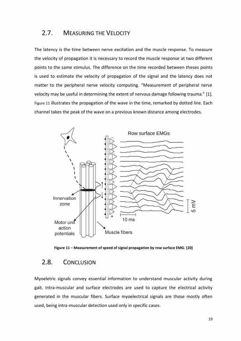
The latency is the time between nerve excitation and the muscle response. To measure
the velocity of propagation it is necessary to record the muscle response at two different
points to the same stimulus. The difference on the time recorded between theses points
is used to estimate the velocity of propagation of the signal and the latency does not
matter to the peripheral nerve velocity computing. “Measurement of peripheral nerve
velocity may be useful in determining the extent of nervous damage following trauma.” [1].
Figure 11 illustrates the propagation of the wave in the time, remarked by dotted line. Each
channel takes the peak of the wave on a previous known distance among electrodes.
Figure 11 – Measurement of speed of signal propagation by row surface EMG. [20]
2.8. CONCLUSION
Myoeletric signals convey essential information to understand muscular activity during
gait. Intra-muscular and surface electrodes are used to capture the electrical activity
generated in the muscular fibers. Surface myoelectrical signals are those mostly often
used, being intra-muscular detection used only in specific cases.
Row surface EMGs

20
Myoeletric signals present specific frequency and amplitude characteristics which,
although not very demanding, require the use of specific conditioning circuits and
processing operations.
This chapter presents a brief overview on the origin of myoeletric signals, its
characteristics as well as their use for gait analysis, which helps understanding the context
on which the present work has been developed and provides preliminary information to
better understand next chapters.

21
3. TECHNOLOGIES
This chapter provides an introduction to the main technologies involved in the design of
the data capture and transmission system developed in this dissertation. This system can
be seen as part, a node, of a wireless sensor network and thus the technologies being
described here are in fact those commonly found in these wireless systems.
The concept of Wireless Sensor Network (WSN) applied to BSN has been developing,
mainly since the 1990 decade. The architecture of each node of a sensor network
comprises mainly a unit processor, sensor interface, power supply, memory, wireless
connection, and an Operating System (OS) (Figure 12).
Figure 12 - The main components of common WSN nodes.
- Processor
The devices used in a WSN are required to present low processing power due to
constraints in size and power consumption. For this reason, simple Microcontroller Units
(MCUs) are used in the WSN sensor nodes.
- Memory
Memory is useful in embedded systems to store configuration information, programs
images or as an immediate buffer to store data sampled from sensors. Sometimes it is
necessary to overcome the limited Random Access Memory (RAM) present on the MCU
with some additional external memory, typically a flash memory or an Electrically
Erasable Programmable Read-Only Memory (EEPROM). The advantage of using this kind
of memory is that it does not need power to retain the stored data.

22
- Sensors interface
Sensors can delivery either analogue readings, requiring the existence of an Analog -
Digital Convertor (ADC) interface for data sampling and acquisition, or digital data,
requiring the usage of a protocol to establish a communication with MCU. The most
widely used communication protocols are Serial Peripheral Interface (SPI), Integrated
Interconnect (I²C) and Universal Asynchronous Receiver - Transmitter (UART).
- Power supply
The power supply is the main determining factor of the size, volume, and autonomy of
the WSN hardware [21]. More popular power sources are Li-ion batteries, zinc-air
batteries and rechargeable batteries. Different energy harvesting schemes have also been
proposed to increase the operation autonomy of remotely deployed sensor nodes [22].
- Operating system
Usually a proprietary developed firmware is used in many cases, but when the complexity
of the system increases it is required the usage of an OS. Despite the widely introduction
of proprietary OS, the open source OS is yet the mostly used for embedded systems,
mainly the C-based OS.
- Wireless Communication
Usually the wireless communication is the operation that requires the highest power
consumption. In some cases this component is responsible for even more than 50% of
whole power required by the sensor node. For that reason a significant effort has been
concentrated on the development of efficient-energy protocols and routing strategies.
“For many WSNs, node size and power consumption are often considered
more important than the actual processing capacity because in most
applications the amount of processing involved is relatively light.” [21]
The architecture adopted depends mainly on the WSN application. What different
architectures have in common is the needs of low power consumption, being the
differences related to number of sampling channels, sampling rate and the amount of
data processing. These variables affect the choice of the MCU in terms of power
processing, data rate, clock frequency, required peripherals, and number of Input /

23
Output (I/O), determining what node platform to be adopted. Nowadays there are several
different architectures found in WSN applications. Some are more notable either by their
pioneering or by their wide referencing. Table 3 lists some of them and their features.
Table 3 – Most notorious WSN node platform with their features. [21].
Platforms CPU Clock (MHz)
RAM / Flash /
EEPROM Transceiver
Bandwidth (kHz)
Frequency (MHz)
OS
BSN node TI
MSP430F190 8
2k / 60k / 512k
Chipcon CC2420
250 2400 Tiny OS
BT node Atmel Atmega
128L 8
4k / 128k / 4k
ZV4002 BT/CC1000
1000 2400 Tiny OS
Dot Atmel Atmega
163 8
1k / 16k / 32k
RFM TR1000 10 916.5 Tiny OS
EnOcean TCM120
PIC18F452 10 1.5k / 32k
/ 256 Infineon TDA5200
120 868 Tiny OS
EyesIFX v2 TI
MSP430F1611 8 10k / 48k
Infineon TDA5250
64 868 Tiny OS
iMote1 Zeevo ZV4002
(ARM) 12 - 48
64k / 512k
Zeevo BT 720 2400 Tiny OS
iMote2 Intel PXA 271 13-140 128k / 32M
CC2420 250 2400 Tiny OS
Mica Atmel Atmega
128L 4
4k / 128k / 512k
RFM TR1000 40 916.5 Tiny OS
Mica2 Atmel Atmega
128L 8
4k / 128k / 512k
Chipcon CC1000
38.4 900 Tiny OS
Mica2Dot Atmel Atmega
128L 4
4k / 128k / 512k
Chipcon CC1000
38.4 900 Tiny OS
MicaZ Atmel Atmega
128L 8
4k / 128k / 4k
Chipcon CC2420
250 2400 Tiny OS
Nynph Atmel Atmega
128L 4 4k / 128k
Chipcon CC1000
38.4 900 Mantis
Particle2/29 PIC18F6720 20 4k / 128k
/ 512k RFM TR1001 125 868.35 Smart-its
Rene Atmel
AT90LS8535 4
512 / 8k / 32k
RFM TR1000 10 916.5 Tiny OS
Sun Spot Atmel
AT91FR40162S 75
256k / 2M
CC2420 250 2400 Squawk
VM(Java)
Telos TI
MSP430F149 8
2k / 60k / 512k
Chipcon CC2420
250 2400 Tiny OS
T-Mote Sky TI
MSP430F1611 8
10k / 48k / 1M
Chipcon CC2420
250 2400 Tiny OS
U3 PIC18F452 0.031-8 1k / 32k /
256 CDC-TR-02B 100 315 Pavenet
XYZ OKI
ML67Q500x (ARM/THUMB)
1.8 - 57.6
4k / 256k / 512k
Chipcon CC2420
250 2400 SOS
Wec Atmel
AT90LS8535 4
512 / 8k / 32k
RFM TR1000 10 916.5 Tiny OS

24
3.1. NETWORK TOPOLOGIES
Concerning communications topologies two terms can be distinguished: the physical
topology refers to the structure of connection, and the logical topology refers to the data
and packed exchange way. Within the Open System Interconnection (OSI) model “the
physical layer and data link layer, define the physical topology of a network, while the
network layer is responsible for the logical topology.” [7]
In the physical topology the participants can be connected in a point-to-point framework,
star, mesh, star-mesh hybrid and cluster tree framework. Figure 13 illustrates each one of
these topologies.
(a)
(b)
(c)
(d) (e)
Figure 13 - Basic network topologies: (a) Point-to-point, (b) Star, (c) Mesh, (d) Star-Mesh hybrid, (e)
Cluster tree. [7]
The main application of WSN in medical monitoring is on non intrusive cases. BSN can be
employed either in a stand-alone context or in combination with mobile phones or
ambient sensors networks [7].

25
In the stand-alone context it has usually a processing unit conjointly with the sensing
functions. The processing unit reads and records bio-signals or quantities like EMG, ECG,
EEG, bloody pressure, and blood flow. Depending on the context, theses signals can be
used together with signals provided by other types of sensors like accelerometers,
thermometers or gyro-meters. The star topology is the most widely employed in these
applications, being necessary an intelligent central unit. Mesh topologies can be found in
the same applications in continuous non-invasive monitoring, but in this case it becomes
necessary to endow the sensors with some intelligence to operate independently from a
central unit.
Figure 14 - “Star vs. mesh-based body sensor network.”[7]
Figure 14 presents a comparison between the most used topologies. The star topology
takes advantage over mesh by its simplicity, low power consumption, high bandwidth and
low latency. On the other hand, the mesh topology takes advantages considering fault
communications robustness, reliability and large spatial coverage [7].
In the star topology, the central unit assumes the role of processing and communication
master and needs, sometimes, an additional hardware as a bridge. In the mesh topology
the communication with every sensors implies a higher bandwidth and processing
overhead, being advisable to choose one sensor to act as bridge.

26
3.2. NETWORK CONFIGURATION
The star topology has clear advantage over the mesh topology when low power
consumption is mandatory. Additionally, the use of the MCU acting like coordinator in a
single node fits the requirements of the system based on a star topology. Figure 15 is an
illustration of a MCU based BSN in which electrodes, sensors and CU are the participants.
In this configuration the CU is the master and electrodes and sensors act as slaves. The
master provides the clock and controls the data flow. The MCU endows the CU with
enough ability to act as a bridge, linking parts of networks. The BSN is part of a WSN in
which the CU co-participates. In Figure 15 the external participant to the BSN is a PC
connected in a Peer-to-Peer (P2P) communication mode. MCUs usually are not featured
with wireless connectivity and it is necessary to add a peripheral communication module
to establish a link. The CU can act like a server in the WSN but in the most common
configuration the external participants are responsible to initiate the link.
Figure 15 – WSN and the participants. The node is composed by CU that acts like a bridge.
Figure 15 is the first high level scheme of the planned system. For the present work it is
proper to use a cheap and low-power transceiver for low and moderate data rates. As far
as communication standards are concerned there are some short-range standards to
ensure the interoperability and flexibility of the devices, such as Bluetooth Low Energy
(BT-LE), IEEE802.15.4 (ZigBee) and IEEE802.15.6 (Medical Body-Area Networks - MBAN).

27
3.3. WIRELESS LINK AND PROTOCOLS
“In order to achieve cost-effective, flexible and preferably interoperable
solutions, it is almost a necessity to abandon proprietary technological
approaches and instead choose standardized wireless technology as the
basis of a BSN.”[7]
The use of radio frequency spectrum is internationally regulated after the
communication ranges of the specific applications. Not specified applications are
located in restricted ranges of the spectrum. The devices operating in these intervals
have limitations in power, range and bandwidth. The most important frequency
ranges for BSNs are Very High Frequency (VHF) (< 300 MHz), Ultra High Frequency
(UHF) (e.g. 315, 433, 868 – 928 MHz), the worldwide 2.4 GHz Industrial, Scientific and
Medical band (ISM), the worldwide 5 GHz band, and, for Ultra Wideband (UWB), the 3
– 10.6 GHz band [7].
WLAN and WPAN are issued by IEEE 802.11 and IEEE 802.15 specifications respectively
that establish standards for short range wireless networks. They define the Physical
(PHY) and Medium Access Control (MAC) layers for wireless communications over an
action range around 10 – 100 m. Four main standards based on these specifications
are available in the market. The Wi-Fi standard is based on the IEEE 802.11
specification and is thought to relative high rate data flow. Three other standards,
Bluetooth, ZigBee and UWB, are based on IEEE 802.15, targeting WPAN. Each one has
a dedicated IEEE Task Group that defines its own specification: IEEE 802.15.1 for
Bluetooth, IEEE 802.15.3 for UWB and IEEE 802.15.4 for ZigBee. Generally the WPAN is
more restricted than WLAN in covering power consumption and data flow. The
characteristics of these standards are given in the Table 4.
The UWB is designed for high data rate being suitable for multimedia stream. Its
architecture allows significant power economy regarding the amount of data
processing. Bluetooth is meant to medium data rate using cheap low power devices. It
is the most complex protocol as it implies 188 primitives and events in total. Thus, it
has higher latency among these four standards.
28
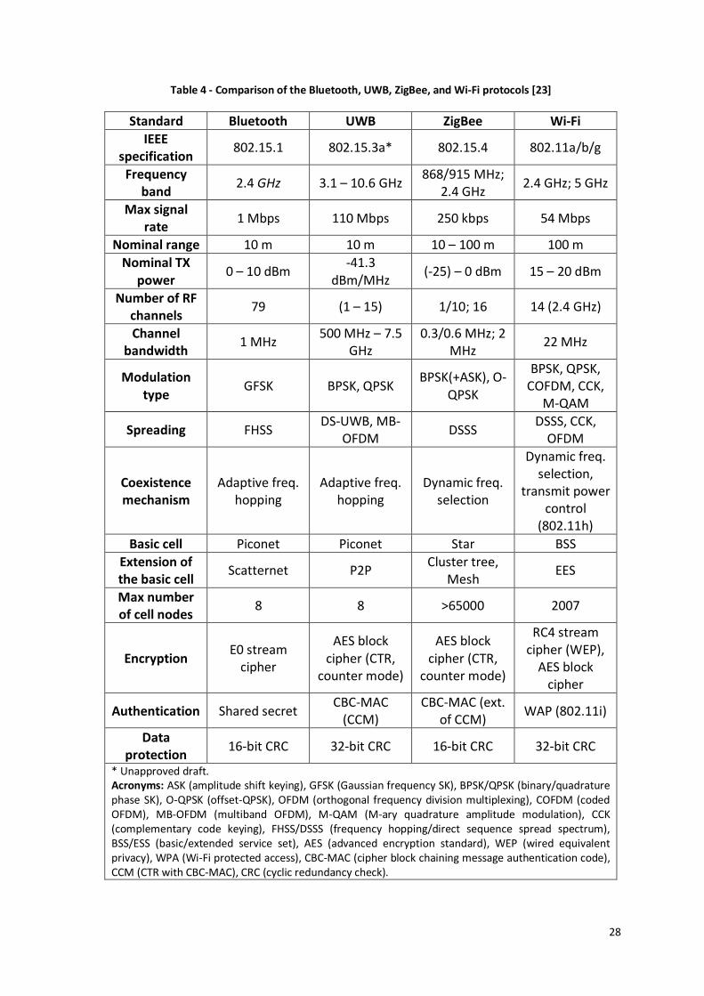
Table 4 - Comparison of the Bluetooth, UWB, ZigBee, and Wi-Fi protocols [23]
Standard Bluetooth UWB ZigBee Wi-Fi
IEEE specification
802.15.1 802.15.3a* 802.15.4 802.11a/b/g
Frequency band
2.4 GHz 3.1 – 10.6 GHz 868/915 MHz;
2.4 GHz 2.4 GHz; 5 GHz
Max signal rate
1 Mbps 110 Mbps 250 kbps 54 Mbps
Nominal range 10 m 10 m 10 – 100 m 100 m
Nominal TX power
0 – 10 dBm -41.3
dBm/MHz (-25) – 0 dBm 15 – 20 dBm
Number of RF channels
79 (1 – 15) 1/10; 16 14 (2.4 GHz)
Channel bandwidth
1 MHz 500 MHz – 7.5
GHz 0.3/0.6 MHz; 2
MHz 22 MHz
Modulation type
GFSK BPSK, QPSK BPSK(+ASK), O-
QPSK
BPSK, QPSK, COFDM, CCK,
M-QAM
Spreading FHSS DS-UWB, MB-
OFDM DSSS
DSSS, CCK, OFDM
Coexistence mechanism
Adaptive freq. hopping
Adaptive freq. hopping
Dynamic freq. selection
Dynamic freq. selection,
transmit power control
(802.11h)
Basic cell Piconet Piconet Star BSS
Extension of the basic cell
Scatternet P2P Cluster tree,
Mesh EES
Max number of cell nodes
8 8 >65000 2007
Encryption E0 stream
cipher
AES block cipher (CTR,
counter mode)
AES block cipher (CTR,
counter mode)
RC4 stream cipher (WEP),
AES block cipher
Authentication Shared secret CBC-MAC
(CCM) CBC-MAC (ext.
of CCM) WAP (802.11i)
Data protection
16-bit CRC 32-bit CRC 16-bit CRC 32-bit CRC
* Unapproved draft. Acronyms: ASK (amplitude shift keying), GFSK (Gaussian frequency SK), BPSK/QPSK (binary/quadrature phase SK), O-QPSK (offset-QPSK), OFDM (orthogonal frequency division multiplexing), COFDM (coded OFDM), MB-OFDM (multiband OFDM), M-QAM (M-ary quadrature amplitude modulation), CCK (complementary code keying), FHSS/DSSS (frequency hopping/direct sequence spread spectrum), BSS/ESS (basic/extended service set), AES (advanced encryption standard), WEP (wired equivalent privacy), WPA (Wi-Fi protected access), CBC-MAC (cipher block chaining message authentication code), CCM (CTR with CBC-MAC), CRC (cyclic redundancy check).

29
ZigBee is the simplest protocol. It is suitable for low data rate, what allows operating with
lower power consumption and provides the smaller latency [7]. Their limited memory and
computational capacity restrings its application to sensor networking.
Wi-Fi is meant for high data rate to expansion of Internet [23]. “IEEE 802.11b transceivers
are far more power-hungry, with typical power consumptions between 400 mW and
1500 mW.”[7] The performance of each protocol regarding the power consumption is
shown in Figure 16, in which the power is given in mW. Figure 17 shows the energy in mJ
required to transmit 1 Mb of data.
Figure 16 – “Comparison of the power consumption for each protocol.” [23]
Figure 17 – “Comparison of the normalized energy consumption for each protocol.”[23]

30
It is possible to conclude from these two graphs that Bluetooth and ZigBee are suitable
for low data rate applications with limited battery power, conditions imposed by a sensor
network. Also ZigBee has slight advantage over Bluetooth in power consumption, lower
latency, flexibility and simplicity but is limited when higher data rates are necessary, what
is the case if it is meant to operate like a gateway of an external network. Considering this
last scenario, one can conclude that Bluetooth is then the better quoted candidate when
the function exceeds the operation in a BSN.
3.4. BLUETOOTH ARCHITECTURE
The Bluetooth standard has been developed by a Special Interest Group (SIG), a gathering
of thousands of companies that keep as an opened industrial specification, allowing all
members using it freely in their products. The idea is creating a universal standard that
allow the operation among different devices regarding the powering and expensiveness
issues. This standard has been used in a wide sort of applications as mobile telephony,
mice, keyboards, PCs, cars, cameras, audio helmets, remote services as banking payment
and so on. Its operation is ensured by a basic layer that supports all protocols from higher
layers and provides services to the applications. In accordance to the application, it is
specified a profile, which “gives details about protocols parameters and settings for
the device to be able to discover these applications and to communicate in a uniform
way” [24]. The most common profiles are:
- Generic Access Profile (GAP)
- Service Discovery Application Profile (SDAP)
- Cordless Telephony Profile (CTP)
- Intercom Profile (IP)
- Serial Port Profile (SPP)
- Headset (HS)
- Dial-up Networking Profile (DNP)
- Fax Profile (FP).
- Local Area Network Profile (LAP)
- Generic Object Exchange Profile (GOEP)

31
- File Transfer Profile (FTP)3
- Synchronization Profile (SP)
The protocol stack is organized in four layers which are opened to other protocols
allowing their interoperability with a sort of communication standards, including with not
specified Bluetooth protocols. Bluetooth has as a principle the maximum reusing of
existent protocols to ensure the smooth operation and interoperability of these
applications [25]. The protocol stack is vertically structured like shown in Figure 18.
Figure 18 - The Bluetooth protocol stack. [25]
The first layer is the “Bluetooth Core Protocol” comprising four protocols: Baseband, Link
Manager Protocol (LMP), Logical Link and Control Adaptation Protocol (L2CAP) and Service
Discovery Protocol (SDP). The second layer is the “Cable Replacement Protocol” that uses
the RFCOMM, which is a protocol that emulates a serial line over Bluetooth baseband, with
RS232 control and data signals. The third layer is the “Telephony Control Protocol” that
comprises Telephony Control Specifications (TCS) – Binary, a bit-oriented protocol that is
used in speech and data exchange services, and AT – commands for FAX services. Finally,
3 It does not mean File Transfer Protocol (FTP), although this protocol is being included in the profile’s
protocol stack.
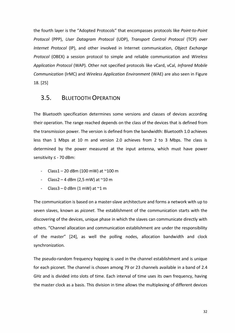
32
the fourth layer is the “Adopted Protocols” that encompasses protocols like Point-to-Point
Protocol (PPP), User Datagram Protocol (UDP), Transport Control Protocol (TCP) over
Internet Protocol (IP), and other involved in Internet communication, Object Exchange
Protocol (OBEX) a session protocol to simple and reliable communication and Wireless
Application Protocol (WAP). Other not specified protocols like vCard, vCal, Infrared Mobile
Communication (IrMC) and Wireless Application Environment (WAE) are also seen in Figure
18. [25]
3.5. BLUETOOTH OPERATION
The Bluetooth specification determines some versions and classes of devices according
their operation. The range reached depends on the class of the devices that is defined from
the transmission power. The version is defined from the bandwidth: Bluetooth 1.0 achieves
less than 1 Mbps at 10 m and version 2.0 achieves from 2 to 3 Mbps. The class is
determined by the power measured at the input antenna, which must have power
sensitivity ≤ - 70 dBm:
- Class1 – 20 dBm (100 mW) at ~100 m
- Class2 – 4 dBm (2,5 mW) at ~10 m
- Class3 – 0 dBm (1 mW) at ~1 m
The communication is based on a master-slave architecture and forms a network with up to
seven slaves, known as piconet. The establishment of the communication starts with the
discovering of the devices, unique phase in which the slaves can communicate directly with
others. “Channel allocation and communication establishment are under the responsibility
of the master” [24], as well the polling nodes, allocation bandwidth and clock
synchronization.
The pseudo-random frequency hopping is used in the channel establishment and is unique
for each piconet. The channel is chosen among 79 or 23 channels available in a band of 2.4
GHz and is divided into slots of time. Each interval of time uses its own frequency, having
the master clock as a basis. This division in time allows the multiplexing of different devices
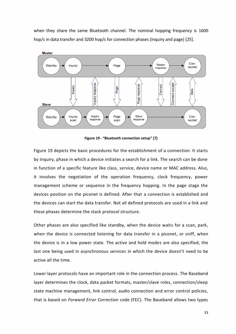
33
when they share the same Bluetooth channel. The nominal hopping frequency is 1600
hop/s in data transfer and 3200 hop/s for connection phases (inquiry and page) [25].
Figure 19 - “Bluetooth connection setup” [7]
Figure 19 depicts the basic procedures for the establishment of a connection. It starts
by Inquiry, phase in which a device initiates a search for a link. The search can be done
in function of a specific feature like class, service, device name or MAC address. Also,
it involves the negotiation of the operation frequency, clock frequency, power
management scheme or sequence in the frequency hopping. In the page stage the
devices position on the piconet is defined. After that a connection is established and
the devices can start the data transfer. Not all defined protocols are used in a link and
these phases determine the stack protocol structure.
Other phases are also specified like standby, when the device waits for a scan, park,
when the device is connected listening for data transfer in a piconet, or sniff, when
the device is in a low power state. The active and hold modes are also specified, the
last one being used in asynchronous services in which the device doesn’t need to be
active all the time.
Lower layer protocols have an important role in the connection process. The Baseband
layer determines the clock, data packet formats, master/slave roles, connection/sleep
state machine management, link control, audio connection and error control policies,
that is based on Forward Error Correction code (FEC). The Baseband allows two types

34
of connection in two different physical links: Synchronous Connection-Oriented (SCO)
and Asynchronous Connectionless (ACL).
LMP sets up, authenticates and configures the link. The Inquiry is not a state managed by
the LMP, made by a higher layer protocol HCI. The LMP procedures include the
connection phase, the detach phase, power control and adaptive frequency hopping,
important to the power control procedure. The page process is necessary in the inquiry
state to recognize a possible device that wants to establish a connection, substituting its
address. If none connection is needed, the node goes automatically to the standby state.
The LMP works with the L2CAP to adapt the upper layer protocols to the Baseband. The
SDP provides information about devices, services and characteristics of services necessary
to the establishment of the link.
3.6. THE BLUETOOTH MODULE RN41
RN41 is a certified Bluetooth radio transceiver meant for low power applications. It
delivers up to 3 Mbps data rate for distances over 100 m thanks to an on chip high
performance antenna. The output transmitter power is 12 dBm and the typical receive
sensitivity value is -80 dBm. This device pertains to the class 1 radio and supports versions
2.1, 2.0, 1.2, 1.1 and 2.1 with Enhanced Data Rate (EDR). The frequency of operation
ranges between 2402 MHz and 2480 MHz in which FHSS/GFSK modulation is used with 79
channels at 1 MHz intervals. The embedded stack protocol includes GAP, SDP, RFCOMM
and L2CAP with SSP/DUN and HID profiles. Also it supports HCI interface protocol[26].
The device will be presented in Figure 24.
3.7. THE PROCESSOR
The MCU performs the role of master and its functions are: organizing the data in the
sampling process, receiving data in orderly way, multiplexing data before being sent by
the transceiver. In synchronous tasks the MCU also provides the clock, having as the
source either an internal or external oscillator. A MCU combines in the same chip a
microprocessor and the relevant peripherals, what freed the hardware from additional
external circuitry.
35
Low power systems imply minimal hardware as well as a minimal processing. In this
regard, the intention is not to use buffered data that would imply additional read and
write routines and also the use of additional memory. This approach is feasible if the data
sending happens at the same rate as it is sampled. Some applications require increased
number of input for the sampling process, as in the case of a BSN, for example. It is
recommended using a MCU with additional number of ADC inputs, which avoids using an
external ADC module.
Regarding a BSN, the sampling process is maybe the principal task of the MCU together
with the multiplexing. Both are relatively simple tasks and dispense powerful processors.
If more complex data treatment is necessary and it is possible to transfer the processing
task to another point not battery powered, this may be regarded. Otherwise more
powerful processors like a DSP can be adopted, but this should be avoided due their
relative high consumption [15].
3.8. THE PIC18F14K22
The PIC18F14K22 makes part of the midrange MCU of MicrochipTM, a family of devices
that allies high computational performance and low pin counting. Also they are featured
with high endurance Flash program memory what increases their life. The incorporation
of nano Watt XLP technology reduces significantly the power consumption featuring
these devices with multiple Idle modes, means that the power consumption can be
reduced to 4% of normal operation. In particular, the PIC18F14K22 high performance is
ensured by a Reduced Instruction Set Computer (RISC) Central Processing Unit (CPU)
capable to execute 16 MIPs and an internal oscillator that affords eight options of
frequency, ranging between 31 kHz and 16 MHz. The frequency can be multiplied by 4
with a Phase Lock Loop (PLL) and reach 64 MHz using the internal oscillator. Two
programmable I/Os for external oscillator for customized frequency with equal upper
limit of 64 MHz are also available [27].
This MCU counts with an ADC module with 12 input channels and 10 bits resolution; with
an analog comparator; with 17 I/O pins; with 4 timers / counters, of which 3 with 16 bit –
prescaler and 1 with 8 bit – pre/postscaler; with Enhanced Capture / Compare / Pulse

36
Width Modulation (PWM) - (ECCP) up to 4 PWM outputs; with a Master Synchronous
Serial Port (MSSP) module with SPI and I²C in master and slave modes; and with an
Enhanced Universal Synchronous Asynchronous Receiver Transmitter module (EUSART).
Also it is featured with program memory with 16 kbytes and data memory with 512 bytes.
The devices also present 30 interrupt sources with two levels of priority. The device
scheme can be sow in Figure 22.
3.9. SENSING DEVICES AND INTERFACE
Two types of sensors satisfy the requirements of this project: surface electrodes and
accelerometers. The walking task does not demand a powerful accelerometer. The
SCA3000-D01 is a three axes accelerometer targeted for battery operated devices that
requires low power consumption. The acceleration is measured by a capacitive sense
element that consists of three acceleration sensitive masses. The measurement axes are
rotated 45° compared to the conventional orthogonal (x, y, z) coordinate system. The
signal is filtered and mapped onto the orthogonal coordinates after an AD conversion and
multiplexing. This device is also featured with an internal oscillator and a non-volatile
memory that provides some autonomy. The SCA3000-D01 ensures high performance
even in low power systems thanks to a “robust, stable and low noise and power
capacitive sensors” [28].
This accelerometer is featured with a SPI interface and allows for a master and slave
mode operation. It has the option of being used in the measurement mode, in which
returns the acceleration value, in motion detection mode, in which an interrupt is
generated when a threshold level is exceed, and in free – fall detection modes, that works
similarly to the motion detection mode, differing by the availability of acceleration data
readings. An internal temperature sensor also enhances the accelerometer and it is
available to external reading. The device is presented in Figure 23 [29].
Figure 20 shows the surface electrodes used for general biosignal capturing. Three
electrodes collect one sampling point. The electrodes have the central part within
conductive gel. The EMG conditioning module (Analog Front End - AFE) shown in Figure
25 has been used to interface the acquired signal to the system. This module was

37
developed in INESC – Porto, being constituted by an input instrumentation amplifier with
gain of 5 followed by two amplification stages: the first is a low-pass filter with gain of 20
and cut-off frequency about 480 Hz; the second is an amplifier with variable gain limited
onto 10. The circuit presents an alternative low-pass filtered output, beyond the not
filtered output, with cut-off frequency about 1.6 kHz.
Figure 20 – Top and bottom view of electrodes used in EMG.


39
4. THE DESIGN OF THE SYSTEM
This chapter discusses the three main topics involved in the integration of the final
system. The initial section describes the steps to design the hardware, detailing the
electrical requirements to link and interconnect the devices, when the final hardware is
presented. The devices need to be configured and correctly programmed to establish
communications and to comply with the system constraints and requirements, being the
firmware another important aspect to be discussed. Finally, the last subject to be
addressed is the software deployment and the interaction with the firmware.
Figure 21 – Block diagram to the intended hardware system.
4.1. THE HARDWARE
The system in Figure 21 is proposed following the usual architecture described in Figure 12.
The hardware core is composed by the microcontroller PIC18F14K22 and by the
Bluetooth module RN41 linked through an USART interface. The system periphery is
composed by sensors (accelerometers and electrodes). The accelerometer SCA3000-D01
communicates with the MCU by a SPI interface. The ADC available in the MCU is used to
sample and to convert the EMG signal, which is previously conditioned in the EMG

40
conditioning module. Additional circuitry allows programming the MCU. The ICSP is the
interface used between the programmer device and the MCU. Other required circuits are
the power supply voltage regulator and the power on reset.
To interconnect the devices it is necessary to use a communication protocol. SPI is the
serial communication protocol used to interface the accelerometer to the MCU. Between
the transceiver and MCU the USART protocol is used. The ICSP is the physical interface
used to program the MCU.
4.1.1. THE PIC18F14K22 CHARACTERISTICS
All functions of the PIC18F14K22 MCU are distributed over 20 programmable pins, as
shown in Figure 22. The pin diagram is summarized in Table 6 and the main features and
electrical characteristics are given in Table 5 [27].
Figure 22 – PIC18F14K22 pinouts [27].
Table 5 – Main features and electrical characteristic of PIC18F14K22.
Description Features/Characteristic
Extended Voltage Range 1.8 V – 5.5 V (± 0.3 V)
Program memory 16 kbytes
Data Memory 512 Bytes
Operating Frequency DC – 64 MHz
Max current (run) 14.6 mA (at 5 V and 64 MHz)
Current (sleep mode) 34 nA
Max current I/Os (skin/source) 25 mA
I/O ports A, B and C
Serial communication MSSP (SPI, I²CTM), EUSART
Timers 4
ADC module 12 channels
ECCP module 1

41
Table 6 - PIC18F14K22 pin summary.
Pin name Description Pin number
VDD Ground ref. for logic and I/O 1
RAx / RBx / RCx Digital I/O 2, 3, 4, 5, 6, 7, 8, 9, 10, 11, 12,
13, 14, 15, 16, 17, 18, 19
ANx ADC channel 3, 7, 8, 9, 12, 13, 14, 15, 16, 17,
18, 19
OSCx Oscillator crystal / external clock input 2, 3,
CLKIN External clock source input. 2
CLKOUT OSC2 pin outputs CLKOUT 3
TxxCKI Timer external clock input 2, 17
MCLR Active-low Master Clear 4
VPP High voltage programming input 4
CCP1 Capture/Compare/PWM 5
P1A / P1B / P1C / P1D Enhanced CCP1 PWM output 5, 6, 7, 14
CxOUT Comparator output 6, 17,
SRNQ / SRQ SR latch output 6, 17
C12INx- Comparator C1 and C2 non-inverting
input 7, 14, 15, 18
PGM ICSP™ programming clock pin 7
SS SPI slave select input 8
SDO SPI data out 9
TX EUSART asynchronous transmit 10
CK EUSART synchronous clock 10
SCK / SCL Synchronous serial clock input/output
(SPI and I2C modes) 11
RX EUSART asynchronous receive 12
DT EUSART synchronous data 12
SDI SPI data in 13
SDA I²C™ data I/O 13
CxIN+ Comparator non-inverting input 16, 19
INTx External interrupt 17, 18, 19
PGC ICSP™ programming data pin 18
VREF+ ADC and DAC high reference voltage 18
VREF- ADC and DAC low reference voltage 19
CVREF DAC reference voltage output 19
PGD ICSP™ programming data pin 19
VSS Ground ref. for logic and I/O pins 20
4.1.2. THE ACCELEROMETER ELECTRICAL CHARACTERISTICS
The application requires that the accelerometer being used operates in the measurement
mode. In this mode each axis is read with a resolution of 12 bits. A 13th bit is used as sign.
Therefore two bytes are used to read an entire axis being the three least significant bits

42
(LSb) not used. A complete reading of one point, what means the three axes, uses six
bytes. Thus it is possible to read a range between -2 G and +2 G with 1333 counts/G.
These parameters are summarized in Table 7, together with other relevant features [28].
Table 7 – SCA3000-D01 electrical characteristic [29] [28].
Description Value
Supply voltage 2.35 V – 3.6 V
I/O voltage 1.7 V – 3.6 V
Current consumption at 2.5 V 480 µA (typ)
at 3.3 V 650 µA (typ)
Measuring range ± 2 G
Resolution 0.75 mG / 0.04°
Sensitivity 1333 counts / G
Output buffer 64 samples / axis
Max. SPI clock rate 1.6 MHz
Table 7 also shows the main electrical characteristic of the device that drains relatively
low power, requiring a supply source ranging between 2.35 V and 3.6 V. The maximum
clock rate allowed in communication with others device is 1.6 MHz. The SCA3000-D01 is
available in a package with eighteen pins, being eight of them used. Figure 23 shows this
device soldered on a Printed Wire Board (PWB) and the pinout description is given in
Table 8.
Table 8 – Accelerometer PWB pinout.
Pin Number Pin Name Description
1 VIN Supply Input
2 RST Reset
3 INT Interrupt
4 MOSI Data Out
5 MISO Data In
6 SCK Serial Clock
7 CSB Chip Select
8 GND Ground
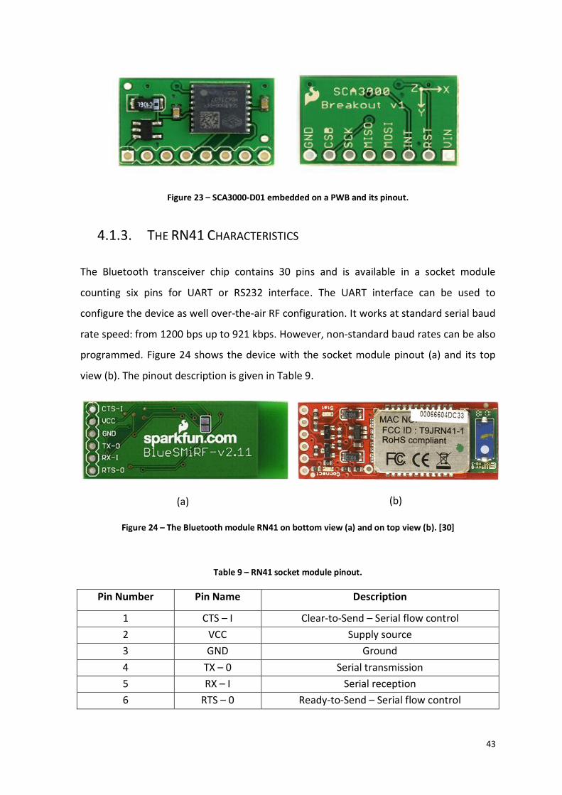
43
Figure 23 – SCA3000-D01 embedded on a PWB and its pinout.
4.1.3. THE RN41 CHARACTERISTICS
The Bluetooth transceiver chip contains 30 pins and is available in a socket module
counting six pins for UART or RS232 interface. The UART interface can be used to
configure the device as well over-the-air RF configuration. It works at standard serial baud
rate speed: from 1200 bps up to 921 kbps. However, non-standard baud rates can be also
programmed. Figure 24 shows the device with the socket module pinout (a) and its top
view (b). The pinout description is given in Table 9.
(a)
(b)
Figure 24 – The Bluetooth module RN41 on bottom view (a) and on top view (b). [30]
Table 9 – RN41 socket module pinout.
Pin Number Pin Name Description
1 CTS – I Clear-to-Send – Serial flow control
2 VCC Supply source
3 GND Ground
4 TX – 0 Serial transmission
5 RX – I Serial reception
6 RTS – 0 Ready-to-Send – Serial flow control

44
The electrical characteristics of this module are summarized in Table 10 where one can
find the power consumption required for transmission and reception conditions. This
devices drain energy when it is connected even without transmission. According to the
Bluetooth specification, the RN-41 is featured with power saving modes that reduce the
standby consumption. In the Sniff mode the device wakes in specific intervals from
sleeping. In the Deep Sleep mode the device is shut-down and the firmware stops its
operation until an external order. The current value for each mode is given in Table 11 [31].
Table 10 – RN41 electrical characteristic [26].
Parameter Min. Typ. Max.
Supply Voltage (DC) 3.0 V 3.3 V 5.0 V
RX supply current - 35 mA 60 mA
TX supply current - 65 mA 100 mA
RF transmit power 12 dBm
Sensitivity -80 dBm
Data rate 1200 bps ~ 921 kbps
Frequency 2402 ~ 2480 MHz
Table 11 – Average power consumption regarding the operation mode [26].
Operation Mode Average Power Consumption
Standby/Idle (default settings) 25 mA
Standby/Idle (deep sleep enable) 250 µA (min.); 2.5 mA (typ.)
Connected (normal mode) 30 mA
Connected (low power sniff) 8 mA
4.1.4. EMG CONDITIONING MODULE
The EMG conditioning module delivers a filtered and amplified analog signal to the MCU.
The accepted amplification level can be programmed on the MCU. Figure 25 (a) is the top
view of the module, in which it is possible to identify a four connections terminal.
Terminal 1 (red marked) is one pole of the EMG input. The other pole is connected in
input 3. The fourth input connects the reference electrode and the second input is meant
to the cable’s shield. Figure 25 (b) shows the bottom view of the module in which six
terminals can be identified. These terminals are used to communicate with other devices

45
and each function is described in the Table 12. The two first pins are voltage input and
reference to supply the module. The following pins are outputs to be used in ADC
function in MCU. The third pin delivers the high voltage reference for the A/D converter.
The low voltage reference is taken in pin four. The fifth pin is the EMG analog output and
the sixth is the filtered EMG signal.
(a)
(b)
Figure 25 – EMG conditioning module (a) top view (b) bottom view.
Table 12 – I/O reference to the EMG conditioning module.
Pin Direction Function Feature
1 Input Vin 3.3 V
2 Input Ground -
3 Output Vref 3.3 V
4 Output Vref / 2 1.15 V
5 Output Va/D1 Not low filtered
6 Output Va/D2 Low filtered
4.1.5. SPI INTERFACE
The SPI protocol is the serial interface used between MCU and accelerometer. The SPI is a
full-duplex synchronous communication. It requires 4 lines, in which 2 lines for data
transfer: Master Input / Slave Output – MISO and Master Output / Slave Input – MOSI.
Another line is used as a Chip Select (SSx) and the last one is the clock. The data
MISO/MOSI and CLK are available for all slave devices through the bus and the data is
transferred when the SS of one device goes to logical level ‘0’. Figure 26 shows the
configuration to multiple slaves.
To link the accelerometer to the MCU it is recommended to use pull-up and pull-down
resistors [27] [28]. Table 13 gives the pull-up / pull-down resistors values and the
available commercial values [28]. The SDA3000-D01 documentation omits any

46
recommendation to a pull resistor at MISO line. However, this recommendation is
provided in the MCU documentation, in which the MCU port current value is used to
compute the pull-down resistor value [27].
Figure 26 – SPI configuration for multiple slaves. The MISO, MOSI and CLK signal are available on a bus.
Table 13 – Recommended resistor value for stable operation.
Pin Direction Resistor V Imax(mA) R(kΩ) =
V/Imax
R-comercial (kΩ -
1/4W)
CSB input pull-up 3.3 0.05 66 68 / 62
XRESET input pull-up 3.3 0.01 330 330
MOSI input pull-down 3.3 0.05 66 68 / 62
SCK input -
-
MISO* output pull-down* 3 0.250 12 12
INT output -
-
* Value recommend to MCU by its datasheet [27].
The communication is made over a 16 bits frame format (Figure 27). The six first bits are
the address of the register to be accessed. The 7th bit defines if the operation is read (‘0’)
or write (‘1’). The eighth bit is not used and is read as ‘0’. If a write operation is
performed, the following eight bits contain data; otherwise, if it is a read operation, these
bits are ignored. These operations are initiated by the master and are done over MOSI
line. At the slave side the first byte answers the previous SPI frame with an error frame at
second bit. The seventh bit is always ‘1’ and the eight bit is the odd parity. The following
byte over MISO line contains the data captured following the read operation. Bits from
the MOSI line are sampled in on the rising edge of SCK and bits to MISO line are latched
out on falling edge of SCK. The read and write operations occurs as shown in Figure 27.

47
Figure 27 – SPI line operations [28].
The read can be made directly in each register or continuously using the decrement
register read. Table 14 details the registers addresses for each byte of specific axes of the
SCA3000-D01. This is the value to be written over MOSI line to do a read operation.
Table 14 – Registers addresses for read operation to SCA3000-D01.
Address Axis Frame
04h X LSB
05h X MSB
06h Y LSB
07h Y MSB
08h Z LSB
09h Z MSB
4.1.6. USART INTERFACE
The USART is a serial I/O communications protocol used among peripherals, also known
as Serial Communications Interface (SCI). It uses four lines in the synchronous mode to
emulate RS232 communications and two lines in the asynchronous mode. In the
synchronous mode the communication is done in half-duplex way. The TX is used as a
bidirectional data line and RX is used as a synchronous clock line. The CTS and RTS are
used to control the data flow. In the asynchronous mode the communication is done in
full-duplex way and CTS and RTS lines are not used. These pins from the RN41 are directly
connected when it operates in asynchronous mode. The MCU’s TX signal is linked to the
RX-I pin of the Bluetooth module and the MCU’s RX signal is connected to the TX-O of the
RN41.
The EUSART transmits and receives the LSb first. The format Non-Return-to-Zero (NRZ) is
used in the transmission and in the reception. An NRZ transmission port idles in the mark
state. Each character transmission consists of one Start bit followed by eight or nine data

48
bits and is always terminated by one or more Stop bits. The Start bit is always a space and
the Stop bits are always marks. The most common data format is 8 bits. These parameters
must have the same configuration in both sides of the line, as well the frequency of
operation.
4.1.7. IN-CIRCUIT SERIAL PROGRAMMING (ICSPTM)
The ICSPTM is the interface used to program PIC microcontrollers and other Microchip
devices in circuit. The programming is done using a device programmer, PICKit2 or PICKit3
for instance, that downloads the program from the developing environment to the target
circuit. The interface requires five signals: VPP, ICSPCLK or PGC, ICSPDAT or PGD, VDD, VSS [32].
- VPP: Is the Programming Voltage that is about +12 V. When applied the device
goes into programming mode.
- ICSPCLK/PGC: Is a unidirectional synchronous serial clock line from the
programmer to the target. This pin needs to be isolated from the application
circuit to prevent signal distortion. A series resistor is a possible solution.
- ICSPDAT/PGD: Is a bidirectional synchronous serial programming data line. This
pin also needs to be isolated. If it is possible, the PGC and PGD should be
dedicated for ICSP.
- VDD: Is the voltage that feeds the target MCU during programming. An external
supply source can be used but typically the circuit is powered by the programmer.
The VDD is +5 V and an isolation circuit is required if the circuit operates at a
different voltage.
- VSS: Is the ground reference that must be at the same potential of the target
circuit.
Figure 28 depicts a possible circuit to isolate the target circuit to the difference of voltage
of the programmer and preserve the signal features. A resistor or a Schottky – type diode
together with a pull-up resistor/capacitor circuit is suggested to isolate the VPP from
circuit preventing the voltage conflict. Two serial resistors also isolate the ICSPDAT and
the ICSPCLK inputs prevent the programming signal degradation.

49
Figure 28 – ICSP circuit interface and isolation circuitry [32].
4.2. THE FINAL HARDWARE
The components were used to assemble the circuit viewed in the Figure 29. There it is
possible to identify the MCU (1), the Bluetooth module (2), the accelerometer (3) and the
EMG conditioning module (4). It is also indicated the ISCP input slot, in which the pin
counting starts from the left side to the right, the output to the EMG sensors, to a scope
and to the source. Auxiliary circuitries complete the mounting as indicated in figure: (A) is
the Reset/ICSP isolation circuit. (D) and (E) are pull-up/pull-down resistors. (B) and (C) are
voltage regulators circuit to 3.3 V and 3.0 V, respectively. The voltage regulator UCC 383-
T3 is used to deliver 3.3 V, where the manufacturer recommended value to the
associated capacitors [33] of 10 µF and 22 µF are used. The FAN 1581 was used to provide
3.0 V using the manufacturer indicated value to the capacitors of 10 µF and 22 µF. The
output voltage is determined by the resistors association. The value of the first resistor
and the typical current is suggested by the manufacturer and the second resistor is
obtained by a voltage divider [34]. The part signaled with (F) is an access point bank for
test purpose with two inputs buffered by the AMPOP LM324N [35]. The schematic with
complete circuit is presented in the Annex B.

50
Figure 29 – Hardware assembly.
4.3. BLUETOOTH MODULE CONFIGURATION
To configure the RN41 module it is necessary to assign a COM port on a PC and connect
through either the Bluetooth or serial port interface. A simple ASCI command language is
used to program and the new configuration take effect after reboot. For over-the-air
configuration the device uses the SPP Service. The pairing process is done manually by the
user using the default key password “1234”. All future connection will be done over the
assigned COM port to this SPP profile. Once connected, the RN41 goes into data mode
and the user has 60 s to go into command mode. A green LED turns on and the red turns
off to indicate that the connection was succeeded [31].
It is in the command mode that all desired configuration and device programming is
done. It is possible to enter in the command mode using an over-the-air connection only
if the device is on the slave mode (default). The command to go into command mode is
“$$$”, typed from a terminal like TeraTerm, HyperTerminal or RealTerm. The OS LinuxTM
incorporates its own terminal, but latter OS WindowsTM releasing does not, being
necessary to install one of them. Once in command mode the Green LED blinks and the
device answers with “CMD”. To exit it type “---<cr>” and the device answers with “END” [31].
The configuration is possible if the serial port parameters are the same for both sides. The
default serial port configuration to RN41 is: 115200 of baud rate, 8 bits, no parity, 1 stop
bit and hardware flow control enabled. Here is present the most important configuration

51
instructions used in the present circuit among a sort of 61. The syntax is the command
followed by a value, both separated by comma. To set the baud rate the command
SU,<value> was used, whose value is one of the serial baud rate standards 1200, 2400,
4800, 9600, 19.2, 28.8, 38.4, 57.6, 115 k, 230 k, 460 k, 921 k. Just the two first characters
are typed in the field value, for example, the baud rate of 115200 was programmed by
the command ‘SU,11’. For non standard baud rates there is the command SZ,<value>, in
which baud rate × 0.004096 determines value. The command SL,N selects none parity.
The module returns “AOK” for a valid command, returns “ERR” for a not valid command
and “?” for a not recognized command [31].
There is the possibility of reducing the module power consumption by configuration
commands. The SJ,<value> command reduces the time window for page scan process and
the SI,<value> command reduces the time window for inquire process. By default, both
values correspond to 12.5% of duty cycle. Values below the default can save power but
under risk to miss an inquiry or page request, whereby these value was maintained. The
activation of the Sniff mode or Deep Sleep mode is the most powerful tool to reduce the
consumption. In both modes the device awakes cyclically under minimal interval of 0.625 ms.
This value is superior to the desired sampling rate (0.5 ms) and their activation would
implies data loosing and was not configured [31].
4.4. THE MCU PROGRAMMING AND CONFIGURATION
The PIC MCU was programmed using C language. The code was developed on the
MPLabTM Integrated Development Environment (IDE) – v8.36 for Windows OS. The MPLab
encompasses the assembler, the linker, the ASM compiler and the simulator in one
environment. A third part is necessary to develop and compile the code in C language,
whereby the MC18 C compiler, specific to the PIC18 family, was installed. The PICKit2
programmer/debugger was used to load the programming to the MCU.
The programming is done writing proper word over specifics feature registers. Some of
them require preprocessing configurations to the MCU start up, what is stored in a non-
volatile memory. The main features to be programmed are the voltage of operation, the
oscillator to be used, the power consumption mode and policies, and boot options. Other

52
initial configurations define how peripherals will behave. Their frequencies are generated
from the oscillator frequency (FOSC) and their instructions are executed in each cycle
period (TCY = 4×TOSC).
- Oscillator:
The oscillator is programmed with 9 registers: CONFIG1H, INTCON, OSCCON, OSCCON2,
OSCTUNE, IPR2, PIE2, PIR2, and T1CON2. With these registers one can configure, for
instance, the system clock, the clock source, the frequency of operation and the startup
mode.
The clock source is chosen among three options, setting the SCS pair bits from the
CONFIG1H register. The options are: Primary External Oscillator (SCS: 00), Secondary
External Oscillator (SCS: 01) and Internal Oscillator (SCS: 1x). The clock sources can
operate in 12 different oscillator modes in which 11 options for external clock source.
As a 13th option the internal oscillator can be clocked out. This oscillator is composed by
two independents oscillators: the LFINTOSC, which provides a low frequency of 31 kHz,
and the HFINTOSC, a high frequency oscillator which provides a range of eight possible
values 16 MHz, 8 MHz, 4 MHz, 2 MHz, 1 MHz, 500 kHz, 250 kHz, 31 kHz. The frequency
of the internal oscillator is set by the bits IRCF<2:0> from OSCCON register. The PLL mode
can be activated through PLLEN bit from OSCTUNE register, multiplying by four standard
frequencies (TCY = TOSC).
All other peripherals share the same clock source, whereby it is necessary to choose the
suitable oscillator frequency to match all their needs. These needs are extended for the
devices linked to the MCU in master/slave architecture to satisfy equally their constraints.
- Interrupt sources:
Twelve registers control the interrupt operation: RCON, INTCON, INTCON2, INTCON3,
PIR1, PIR2, PIE1, PIE2, IPR1, and IPR2. Generally the interrupt control and operation are
done by three bits: the Flag bit to indicate a changing state, the Enable bit to allow an
event to perform an interrupt, and Priority bit to determine the preference on a routine
execution.

53
The PIC18F14K22 peripherals can independently generate interrupt operations in two
possible priority levels: Low and High. To turn on an interrupt source, the GIEL bit of the
INTCON register must be set (‘1’), beyond the correspondent source peripheral Enable
bit. To work with the two priority levels, the IPEN bit of the RCON register must be set
(‘1’) together the GIEH bit of the INTCON register. The source priority with the higher
priority must have its Priority bit set (‘1’). On the operation, the high priority interrupt
level event interrupts the routine flow, even the low priority routine, to perform its
instructions and, in the end, returns to the same point that was stopped. Before returning
to the routine, the interrupt flag bits must be cleared by software, avoiding the
reentrance in the interrupt routine.
- I/O:
Three main registers configure the three I/O ports (A, B and C): the TRIS register defines
the data direction (‘1’ as input, ‘0’ as output); the PORT register reads the levels on the
pins of the device, and the LAT register is the output Latch. Other two registers are
available, one to enable (‘1’) or to disable (‘0’) a weak internal pull-up (WPU register) and
another to enable (‘1’) or to disable (‘0’) the interrupt on-change function (IOC register).
Some port pins share the digital and analog function. When a pin is used as an analog
input, it is necessary to disable the digital input buffer setting the appropriated bit at the
ANSEL and/or ANSELH register. Otherwise, the digital function just performs correctly
with the respectively pin of these registers configured as ‘0’.
- SPI:
The MSSP registers configure the SPI interface by four control registers. The SPI function
is enabled setting the SSPEN bit at SSPCON1 register. Thus, the serial functions (SCK, SDO,
SDI and SS) overlap the I/O port pins. Nevertheless, the respective I/O pin must be
configured either as input or output by TRIS register, regarding the SPI function direction.
The quartet of bits SSPM of this register selects the role to be performed by MCU and the
SPI clock among four options: TMR2/2 (‘0011’), FOSC/64 (‘0010’), FOSC/16 (‘0001’) and
FOSC/4 (‘0000’). The polarity of the clock is defined in the same register by the CKP bit.
Others clock features are configured at the SSPSTAT register, in which the bits SMP and
CKE are used to determine what occasion of the SPI clock cycle the data is sampled and

54
transmitted. CKE and CKP bits determine what the standard SPI mode the bus has been
being configured. Table 15 [27] shows the correspondence between bits configuration
and SPI bus mode.
Table 15 – SPI standard bus modes.
Standard SPI Mode
Terminology
Control bits State
CKP CKE
0, 0 0 1
0, 1 0 0
1, 0 1 1
1, 1 1 0
- USART:
The USART is programmed regarding both, the transmission and the reception functions.
They are enabled writing ‘1’ to the TXEN bit of the TXSTA register, to the CREN of the
RCSTA register respectively, and to the SPEN bit of the RCSTA register. This last bit
enables the EUSART peripheral. The asynchronous communication is configured clearing
the SYNC bit of the TXSTA register.
The analog I/O function must be disabled by clearing the ANSEL bit corresponding to the
TX/CK and RX/DT pins. The TRIS control bits corresponding to the RX/DT and TX/CK pins
should be set to ‘1’. The peripheral will control automatically the pin direction with
EUSART function enabled (SPEN bit set to ‘1’).
The Baud Rate Generator (BRG) is a dedicated timer that operates at 8 bits mode or 16
bits mode. The last referred mode is determined by the BRG16 bit of the BAUDCON
register set (‘1’). The BRGH bit of the TXSTA register set to ‘1’ selects the high baud rate
speed. The baud rate period is configured by the SPBRGH:SPBRG register pair, which
receives the close integer value to the n, determined by Equation 1. The configuration of
BGRH and BGR16 bits determines the k value in the Table 16 to be used in the equation.
The desired baud rate is used to obtain the value of n, including non-standard serial
values, that is computed regarding the frequency of the internal oscillator.
(Equation 1)

55
Table 16 – Value for k in function of the EUSART operation mode.
Configuration Bits BRG/EUSART Mode k
SYNC BGR16 BGRH
0 0 0 8-bit/Asynchronous 64
0 0 1 8-bit/Asynchronous 16
0 1 0 16-bit/Asynchronous 16
0 1 1 16-bit/Asynchronous 4
1 0 - 8-bit/Synchronous 4
1 1 - 16-bit/Synchronous 4
TSR register is the data outgoing register that is not accessible by software. The byte to be
transmitted is written into TXREG and transferred to the TSR register if it is empty. The
transmission starts when the byte is completely transferred. The TXIF bit is controlled by
hardware and is kept cleared while the TSR is busy.
The RSR register is the incoming register that is equally not directly accessible by
software. The accessing to the received data is done via the RCREG register. The RCIF bit
is set whenever there is an unread byte in the input buffer and is cleared when the byte is
read. The RCIF is also controlled by software.
- ADC:
The ADC configuration starts defining the pin analog function, with the ANSx bit of ANSEL
or ANSELH registers corresponding to the analog input set (‘1’). It writing ‘1’ to the TRISx
bit configures the pin as input. The channel to be sampled is determined by the CHS bits
of the ADCON0 register [27]. When changing channels, a delay is required before starting
the next conversion. The delay is configured by ACQT<2:0> bits of the ADCON2 register
among of eight possible multiples to the TAD 0, 2, 4, 6, 8, 12, 16 and 20. TAD is the time to
complete one bit conversion defined in function of the TOSC. 2 TAD wait is required before
the next acquisition can be started. The TOSC is configured by ADCS<2:0> bits also from
ADCON2 register, choosing among seven possible clock frequencies FOSC/2, FOSC/4, FOSC/8,
FOSC/16, FOSC/32, FOSC/64 or FRC.
The ADC module is enabled through ADON bit of the ADCON0 register set to ‘1’. The
sampling starts writing ‘1’ to the GO/DONE bit of the ADCON0 register. The ADIF bit is
automatically set when a conversion is completed and GO/DONE bit is cleared. The ADC

56
sampling has 10 bits of resolution stored in two register: ADRESL and ADRESH. If the
ADFM bit of the ADCON2 register is set, the result is stored in right justified way filling the
LSbs, otherwise, if ADFM bit is clear the result is stored in MSbs and the output format is
left justified. With this resolution readings of 1024 levels between low and high voltage
reference are allowed. The PVCFG and NVCFG bits of the ADCON1 register configure
respectively the positive and negative voltage references. “The positive voltage reference
can be VDD, FVR or an external voltage source. The negative voltage reference can be
either VSS or an external voltage source” [27].
- CCP:
The CCP1 Special Event Trigger can be used to execute a periodic sampling. In this case
the GO/DONE register of the ADCON0 register is controlled by hardware and the Timer1
or Timer3 is used to trigger event. To configure the sampling using the CPP1 with the
Special Event Trigger function, the AD conversion must already be enabled.
To operate in Special Event Trigger mode the CCP1M <3:0> bits of the CCP1CON register
must contain the ‘1011’ bits. This configuration allows the ECCP to reset TMR1 or TMR3,
start AD conversion and set CC1IF bit. These events happen whenever the running timer
value matches to the value written in the CCPR1H and CCPR1L register pair.
- Timers:
TMR1 and TMR3 resemble in their features and configuration. Thus anyone can be
chosen to be used with the Special Event Trigger mode. The choice is done with the
T3CCP1 bit of the T3CON register: ‘1’ selects TMR3 and ‘0’ selects TMR1. Once selected,
the timer must be configured to run as timer mode, clearing the TMRxCS of the TxCON
register. This configuration also selects the FOSC/4 like clock source to the timer. The timer
running frequency is selected by the TxCKPS<1:0> pair bits of the TxCON register among
four prescale options (1:1, 1:2, 1:4 or 1:8). The RD16 bit of this register configures the 8-
bits mode (‘0’) or 16-bits mode (‘1’), depending on the desired running period. The timer
is enabled writing ‘1’ in the TMRxON bit, also in this register. The TMRxH and TMRxL
registers store the running counting that is compared to the CCPR1H and CCPR1L
reference value.

57
- Modes of operation:
There are three possible modes of operation for the MCU, determined by the clock
source and by the fed modules: The Run and Idle modes use any of the three available
clock sources (primary, secondary or internal oscillator block) and the Sleep mode does
not use any clock source. The IDLEN bit of the OSCCON register controls CPU clocking and
the clock source is selected by the SCS<1:0> bits of the OSCCON. All clocks stop with
IDLEN bit cleared and, with the IDLEN bit set, the clock is disconnected from the CPU and
maintained for peripherals.
The power-managed mode is invoked with the ‘SLEEP’ instruction. An interrupt source
can be used to exit from Idle or Sleep mode to the Run mode. The exit sequence is
performed when an interrupt flag bit is set, being necessary the suitable interrupt
configuration in the INTCON and PIE registers.
4.5. THE FIRMWARE
It is possible to distinguish three main steps inside any firmware: the pre-processing
configuration, the initial settings and main code. The pre-processing configurations and
the initial peripherals settings obey the requirements of the tasks performed by the main
code. Here the tasks can be seen slightly into two states as shown in Figure 30.
Figure 30 – Tasks performed in the two states of the main code.
Figure 31 illustrates the basic message exchange between two sides and the action
performed by them. After being turned on and performing the initial settings, the
hardware goes to the low power state, waiting for the link establishment. The PC starts
the Bluetooth communication. The data transfer between two parts also starts with a

58
remote order. When a byte is received, the MCU leaves from idle mode and runs a low
priority routine. The PC also finishes the communication in the same way. Every time that
the low priority routine is called the timer is activated or deactivated by a toggle.
Figure 31 – Handshake diagram between the remote system and the user interface.
Two levels of interrupt priority are defined. The lower level interrupt is called by RC
interrupt flag (Figure 32) and the high level is called by CCP interrupt flag. The first is
activated by a reception of one byte and the second is activated after a CCP triggering.
Once the timer is running, the high priority routine is called whenever a time elapse
happens. Inside this routine, the ADC sampling is performed followed by the transmission
the converted value; followed then by the capture of the accelerometer data and its
transmission. Thus, inside one interrupt routine two bytes are transmitted. The timer is
reactivated at the final of the routine, restarting the process. The system returns
continuously to the idle mode after an interrupt routine is performed. All the time, the
MCU waits by an incoming byte from the PC.

59
Figure 32 – The firmware block diagram.
On the other side, on the laptop, data is received using a GUI application. The user
determines when the link is established and the sampling. The software controls the time
and sends an order to the microcontroller to stop the sampling. The data is received
continuously and processed before being displayed.
4.5.1. THE PACKAGES FORMATION
The samples are sent byte after byte alternating a sampling from one electrode and a
byte from the inertial sensor. The EMG sampling value is sent in one byte. The reading of
one axis of the accelerometer is sent in two bytes and the complete reading of one point
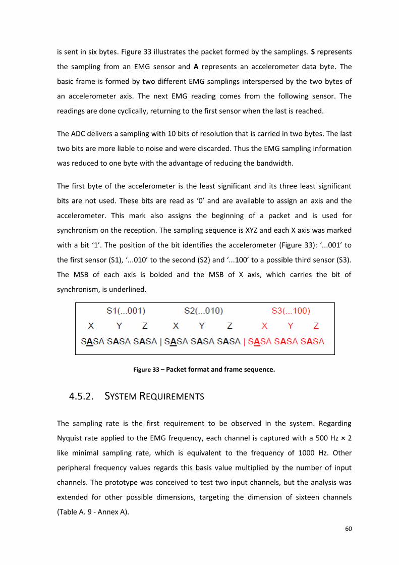
60
is sent in six bytes. Figure 33 illustrates the packet formed by the samplings. S represents
the sampling from an EMG sensor and A represents an accelerometer data byte. The
basic frame is formed by two different EMG samplings interspersed by the two bytes of
an accelerometer axis. The next EMG reading comes from the following sensor. The
readings are done cyclically, returning to the first sensor when the last is reached.
The ADC delivers a sampling with 10 bits of resolution that is carried in two bytes. The last
two bits are more liable to noise and were discarded. Thus the EMG sampling information
was reduced to one byte with the advantage of reducing the bandwidth.
The first byte of the accelerometer is the least significant and its three least significant
bits are not used. These bits are read as ‘0’ and are available to assign an axis and the
accelerometer. This mark also assigns the beginning of a packet and is used for
synchronism on the reception. The sampling sequence is XYZ and each X axis was marked
with a bit ‘1’. The position of the bit identifies the accelerometer (Figure 33): ‘...001’ to
the first sensor (S1), ‘...010’ to the second (S2) and ‘...100’ to a possible third sensor (S3).
The MSB of each axis is bolded and the MSB of X axis, which carries the bit of
synchronism, is underlined.
Figure 33 – Packet format and frame sequence.
4.5.2. SYSTEM REQUIREMENTS
The sampling rate is the first requirement to be observed in the system. Regarding
Nyquist rate applied to the EMG frequency, each channel is captured with a 500 Hz × 2
like minimal sampling rate, which is equivalent to the frequency of 1000 Hz. Other
peripheral frequency values regards this basis value multiplied by the number of input
channels. The prototype was conceived to test two input channels, but the analysis was
extended for other possible dimensions, targeting the dimension of sixteen channels
(Table A. 9 - Annex A).

61
Under these conditions the sampling process is done at 1/2000 s, or 0.5 ms. This is the
interrupt periodic time interval of occurrence, referred as TSMP. The tasks of sampling the
analog channel (TADC), sampling the inertial sensor (TSPI) and send both bytes (TSENDING)
were calculated to be inside this interval (Equation 2). Additional processing is also
regarded and refers to some extra cycles expended to clear an interrupt flag, to perform
other computations (TPROC):
TADC + TSPI + 2×TSENDING + TPROC < TSMP = 0.5 ms. (Equation 2)
The communication frequencies impose their own limitations to the firmware settings.
The SPI was limited by the accelerometer to a frequency below 1600 kHz and the EUSART
by the sampling rate to the minimal of 384000 bps, which is the closest serial standard
value to the 2 kbytes. Table A. 1 of Annex A has the analysis to all standard serial baud
rates. The baud rate upper limit is determined by protocol, 115200 for transmission over
SPP and about 1 Mbps using other profile like RFCOMM or OBEX. The packet format also
limits the transmission, in which one sampling provides two bytes (accelerometer plus
EMG). In this regard the minimal transmission rate is 4 kbps, rising the minimal frequency
576000 bps.
A reliable A/D conversion is ideally done inside the range of 1 µs to 4 µs for the TAD [27]
(Table A. 6 – Annex A). The TADC depends on the choice of TACQ and the frequency of
operation (Equation 3). Table A. 7 in the Annex A has the evaluation of the frequency –
TACQ association that returns the better option.
TADC = TACQ + 11TAD + 2TAD (Equation 3)
TSPI calculation returns the fastest value of 0,016 ms to a complete cycle of R/W
operation. This value is possible to the minimal FOSC of 4000 Hz. Other possible values are
given in the Table A. 5 – Annex A, which has the complete analysis for the all range of
frequencies available by MCU.
The frequency to the EUSART function was computed using Equation 1 targeting the
standard serial baud rate. The resulting value is the n to be written in the SPBRGH:SPBRG
register pair. Table A. 3 and Table A. 4 of the Annex A provide the complete range of n

62
values, as well as the percentage error due the rounding. The feasible TSENDING are given in
Table A. 2.
It was based on these requirements that the choice for the appropriate oscillator and
suitable timer frequencies to feed other functions was done.
4.5.3. FIRMWARE ALGORITHM
The MCU starts up using the internal oscillator as the clock source and the nominal
voltage of 3.0 V, both programmed in the configuration bit. Complementary
characteristics take place in the main code, in which the frequency was programmed to
run at 16 MHz with factory calibration. The oscillator was programmed to clock the
peripherals when “Sleep” instruction is called, being lead to the Idle mode.
Both the transmission and reception of the EUSART were enabled and configured to work
with a word of 8 bits. RX was programmed to listen continuously and to wake up on a
reception event. The Baud Rate Generator used 16 bits in the high speed. The frequency
was programmed to 115.2 kbauds/s writing the decimal 34 (22h) to the SPBRGH:SPBRG
register pair (Table A. 4 – Annex A). Pin 10 was configured as output to be used like TX
and pin 12 was configured as input to be used like RX, being their analog function
disabled.
The SPI was programmed in the mode 0,0 (Table 15) and the FOSC/16 frequency divider was
selected to generate a clock SPI source of 1 MHz. The MCU was programmed to assume
the master role and the pin 11 was programmed output to provide the clock. The pin 9
was programmed as output and the pin 13 was programmed as input and the analog
function was disabled to work as MOSI and MISO respectively. The function SS was
disabled from the pin 8, measure necessary when the SPI function requires more than
one slave. Pins 6 and 7 were configured to use the I/O function to works like SS, operating
then as output. Also, it was necessary to disable the analog function from pin 7. A third
I/O was reserved to a possible inclusion of one slave.
The ADC was programmed to use an external positive voltage reference and ground as
the negative reference. The voltage reference was programmed to use the analog module

63
as source. The word ‘FFh’ was written in the VREFCON2 register to use the full scale of
3 V. This configuration generates a signal offset equal to half the voltage interval. The
sampling was justified to the left to obtain the eight MSbs. The frequency was
programmed to run at 4 MHz (FOSC/4) and a delay of 12 TAD (Table A. 7 – Annex A) was
introduced to ensure the sampling accurate. The pins 16 and 17 were configured as
inputs and enabled to operate in the analog mode.
Pin 5 was also configured as an output to disable the CCP external capture and program
to be used with a special event trigger. The TIMER3 was programmed to provide the clock
source to the CCP module. The frequency was set to run at a scale of 1:2 of the FCY.
Regarding the IRC frequency, the TIMER3 frequency is 2 MHz. The CPP module counts
1000 cycles from the TIMER3 to generate an interrupt at 0.5 ms, which is equivalent to
writing 03E8h to the CCPR1H:CCPR1L register pair (Table A. 10 – Annex A).
The global peripheral interrupts were enabled allowing the multiple levels of priority.
Each specific peripheral interrupt was disabled, except the two desired peripheral
interrupts: the CCP and the RC. The first was set to call the high priority routine and the
second to call the low priority routine.
The following sequence is performed in the low priority interrupt routine:
Receive the incoming byte (wait for interrupt flag clearing);
Set the address to point to the first accelerometer byte (_adsrs = 4);
Initialize a global counting variable (_commut_SS = 0);
Commute the TIMER3 operation.
The high priority interrupt routine performs the next routines:
Clear AD interrupt flag;
Clear CCP interrupt flag;
Send the A/D value;
Wait for the sending finished;
Commute the analog input channel;
Verify if the address is the first or the last byte of the accelerometer. If true:
o Set the address to the first byte (_adsRS = 4);
o Go to the next accelerometer (_commut_SS = ++_commut_SS & 1);
Enables the Sensor Chip Select pin (_SS_CH[_COMMUT_SS]);
Write the address to be read in the accelerometer;

64
Wait to read the required value;
Send the Accelerometer byte;
Disables all Sensor Chip Select pin;
Go to the next byte address (_ADSRS ++);
The code was implemented following general rules for soft and power efficient
programming [6]: The number of variables was minimized using direct R/W on the
registers; the structure of the code was sized for powers of two; it was preferred the
types char, int and short; the most probably case is the first into verifications cyclist and
the mostly called routines were placed before the less called. The final code is presented
in Annex C and the generated program follows in the media digital Annex.
4.6. THE SOFTWARE
The software functions receive and treat the data stream to be displayed in a graphical
interface. The software was developed in visual C# using the Microsoft Visual Studio 2010
like IDE. Visual C# is an events object-oriented program language which provides a vast
sort of visual libraries that facilitates the programming. The developed application was
thought to interact through a clean, intuitive and friendly window, with a first area meant
to plot the graphic representation of EMG signal and kinetic activity and a second area
reserved to input user commands.
Figure 34 – Form window application fashion.

65
The application interface is shown in Figure 34. The commands were organized at the left
side, where on the top are disposed the commands to determine the duration and to
start the sampling. Commands to plot the received data are disposed below, with option
to save the data or clear the scream to get another sampling. The data is saved in a file
“*.txt” with the possibility to be opened late. Only files that obey the coding rule can be
opened. The application also allows saving a plot area as an image file.
The class serialPort was used to establish the Bluetooth communication. Its properties
configurations are the same for the remote Bluetooth device (baud rate of 115200, none
parity, one stop bits). PortName property matches with the COMPort previously
attributed to the Bluetooth device (COM4). The ReadBufferSize property was configured
to 1048576 bytes.
The data is received continuously during the time chosen by the user. A Timer class
controls the time and finishes the connection when the time elapses. A byte is sent at the
connection instant to order the data transfer. The data is copied to an Array and it is
verified if the stream is corrupted. The verification is done searching for the occurrence of
the two first LSB from the ‘X’ axis from the inertial sensor. The marked bytes are spaced
with 12 bytes. Also it is verified if the fourth byte that came from an accelerometer
corresponds to the LSB ‘Y’ axis. These conditions are the basis to the algorithm:
The 3 last bits from Byte[index] and from Byte[index + 12] != 0;
Both three last bits correspond to a counting sequence: (001 -> 010 ->001)
The 3 last bits from Byte[index + 4] and from Byte[index + 16] == 0;
If one condition is not verified the array is discarded and returns a message error.
Otherwise, the data is computed and the code follows verifying the data bloc length.
Now, if an error is found, only the wrong bloc is discarded and is rebuilt by the arithmetic
mean between the anterior and posterior bloc. This approach is just efficient when few
bytes are lost. If two successive blocs show error the array copy is halted.
The treated array contains alternated data types, being divided in other two arrays, a first
containing just EMG data and a second with all accelerometer measuring. The first array
has data from alternated EMG sensors and a new division for other two arrays is done
separating even and odd elements. The sampling position related to the marked byte (‘X’

66
axis) identifies the sensor origin. Each byte was normalized and extracted the offset to
recover data before plotting. The multiplication by 3 was done to match to the amplitude
reference from EMG module.
ByteToPlot[index] = 3 × (Byte[index] - 127) / 256;
The second array alternates the LSB and the MSB from all axes of the accelerometers. The
accelerometer source alternates for each six bytes. Again the array is divided in other two
arrays in accordance with the assigned bit in the marked byte. The information is
recovered binding the LSB to the next MSB. The three LSbs are ignored and the LSB is
shifted the corresponding positions to the right. The MSB is shifted five positions to the
left and finally the MSB and LSB are bound to form the number of counts measured. The
division for 1.333 (multiplying by 0.75) returns the value of acceleration in gravity to be
plotted in the chart.
Value = ((LSB >> 3) or (MSB << 5)) × 0.75;

67
5. TESTS AND VALIDATIONS
This section presents the results obtained to validate the conceived system. The
validation is done by comparing results to an expected waveform. Some tests done to
verify the right mounting and the fine hardware working flow are also presented.
Preliminary tests were made in order to reproduce the conditions of the real EMG signal.
5.1. MODULE BLUETOOTH - MCU COMMUNICATION
The communication was established over SPP through serial port COMM4 on PC. All the
devices and the COMPort were set to operate on 9600 kbps and the SPP settings was
none parity bit, 1 stop bit.
Three different terminals were used to read incoming data from serial port: Realterm,
Indigo and Teraterm. All of them are similar and they are free for download on the web.
On the test, a string of characters was sent from the MCU to the Bluetooth module, and
then sent to the PC. A single circuit was implemented on a protoboard comprising the
Bluetooth module and the MCU programmed with a ‘Hello World’ firmware. The three
terminals displayed the sent string correctly.
The correct reception within the hardware module was tested altering the firmware to
send a string after receiving a command from the computer. The command was given by
a specific character with the sending occurring after the character is recognized at the
MCU. In this situation the string was also displayed correctly and the orders were obeyed
as expected. This test also worked to verify the link between module and PC.
5.2. SAMPLING TEST
Two signal generators and a scope were used to test the sampling process. The objective
was to sample a known waveform to be recovered in the reception. A new code was
loaded to the MCU keeping the serial communications configurations and adding the ADC

68
settings. The MCU was configured to use the internal voltage reference (FRV) with
positive reference at 1.024 V and negative reference at 0 V. The used sampling rate was
about 15 kHz (1 M/64). Two input channels were enabled and the code alternates the
sampling of the two inputs.
Both signal generators delivered a signal with a frequency of 100 Hz and 0.6 Vpp of
amplitude. The voltage value below 1 V avoids the saturation on the receiver. Also it was
necessary to introduce a 0.5 V of DC offset. One generator delivered a sinusoidal signal to
one input and the other generator delivered a triangular signal to the second input. The
MCU input was isolated using a buffered stage with OPAMP LM324N.
Figure 35 – Sinusoidal signal with frequency of 100 Hz recovered.
Figure 36 – Triangular signal with frequency 100 Hz recovered.
0
100
200
300
400
500
600
700
0 50 100 150 200 250 300
0
100
200
300
400
500
600
700
800
0 20 40 60 80 100 120 140 160 180 200
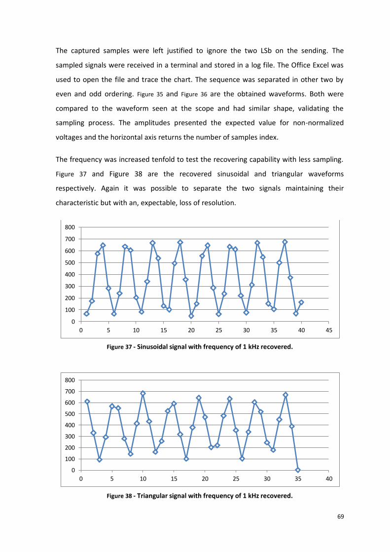
69
The captured samples were left justified to ignore the two LSb on the sending. The
sampled signals were received in a terminal and stored in a log file. The Office Excel was
used to open the file and trace the chart. The sequence was separated in other two by
even and odd ordering. Figure 35 and Figure 36 are the obtained waveforms. Both were
compared to the waveform seen at the scope and had similar shape, validating the
sampling process. The amplitudes presented the expected value for non-normalized
voltages and the horizontal axis returns the number of samples index.
The frequency was increased tenfold to test the recovering capability with less sampling.
Figure 37 and Figure 38 are the recovered sinusoidal and triangular waveforms
respectively. Again it was possible to separate the two signals maintaining their
characteristic but with an, expectable, loss of resolution.
Figure 37 - Sinusoidal signal with frequency of 1 kHz recovered.
Figure 38 - Triangular signal with frequency of 1 kHz recovered.
0
100
200
300
400
500
600
700
800
0 5 10 15 20 25 30 35 40 45
0
100
200
300
400
500
600
700
800
0 5 10 15 20 25 30 35 40

70
5.3. ACCELEROMETER – MCU SPI COMMUNICATION
The firmware was altered to send the SPI data instead of the ADC sampling. The
peripheral was programmed to use two slaves alternately. The frequency used was
(FOSC = 1M) / 4. A scope was used to verify the clock waveform delivered to the slaves.
The scope was also used to verify the SS switching. In these tests the clock presented the
expected waveform and frequency and both SS behaved as desired, switching between
the low and high level alternating the two SS outputs.
The MatLab was used to receive and treat the data from the accelerometer. A *.m file
was prepared to communicate through the serial port and reorder the bytes sequence to
present the sampled acceleration value on the screen. As just one accelerometer was
available, only one channel a time was tested. In this regard, it was expected reading
values ‘0’ for the isolated sensor input. For the axis in vertical position it was expected a
value of about 1333 counts. The opposite value was expected varying the axis position by
180°.
Table 17 – Acceleration value measured for each axis in the vertical position.
Sensor 1 Sensor 2
Position X Y Z X Y Z
X - 0° -1307 -1 -21 0 0 0
X - 180° 1345 66 60 0 0 0
Y - 0° 38 -1179 583 0 0 0
Y - 180° -31 1372 -37 0 0 0
Z - 0° 15 129 1364 0 0 0
Z - 180° -17 64 -1306 0 0 0
X - 0° 0 0 0 -1311 -3 -26
X - 180° 0 0 0 1348 59 42
Y - 0° 0 0 0 34 -1281 168
Y - 180° 0 0 0 -7 1363 -19
Z - 0° 0 0 7 121 1366
Z - 180° 0 0 0 -15 84 -1300
Table 17 is composed by the first obtained values on a set of 64 samples. As the samples
were obtained in hold position, all 64 values are closed. The axis tested was on vertical

71
position, in order to be parallel to the gravity acceleration vector. The color orange
highlights the varied axis and the gray indicates the inactive sensor. The obtained values
are inside the expected values, showing that sensors and the microcontroller output
operate properly.
5.4. TEST TO THE FINAL SYSTEM
The system was programmed to run with final configuration values for all peripherals,
with the purpose of performing a last test before coupling the EMG sensor. The intention
is verifying the joint operation and the fidelity on recovering a waveform in the presence
of the AFE module. A function generator delivers a known waveform in the minimal
allowed voltage (0.1 Vpp). A sinusoidal wave with 1 kHz frequency was applied. The signal
passes through a voltage divider to reduce the input voltage to about 1/10 the maximum
range to avoid saturation. Here the amplification stage was also tested.
Figure 39 – The waveform obtained from the test to the complete system, displayed on the
developed GUI: (a) shows the sinusoidal wave from signal generator; (b) is an unused input
meant to the accelerometer data; (c) shows a 2nd input with three axes accelerometer data.
(a)
(b)
(c)
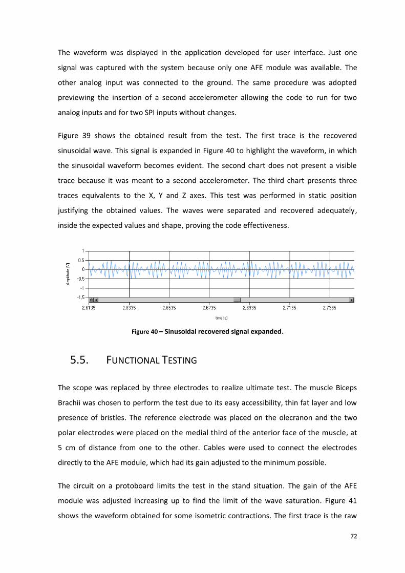
72
The waveform was displayed in the application developed for user interface. Just one
signal was captured with the system because only one AFE module was available. The
other analog input was connected to the ground. The same procedure was adopted
previewing the insertion of a second accelerometer allowing the code to run for two
analog inputs and for two SPI inputs without changes.
Figure 39 shows the obtained result from the test. The first trace is the recovered
sinusoidal wave. This signal is expanded in Figure 40 to highlight the waveform, in which
the sinusoidal waveform becomes evident. The second chart does not present a visible
trace because it was meant to a second accelerometer. The third chart presents three
traces equivalents to the X, Y and Z axes. This test was performed in static position
justifying the obtained values. The waves were separated and recovered adequately,
inside the expected values and shape, proving the code effectiveness.
Figure 40 – Sinusoidal recovered signal expanded.
5.5. FUNCTIONAL TESTING
The scope was replaced by three electrodes to realize ultimate test. The muscle Biceps
Brachii was chosen to perform the test due to its easy accessibility, thin fat layer and low
presence of bristles. The reference electrode was placed on the olecranon and the two
polar electrodes were placed on the medial third of the anterior face of the muscle, at
5 cm of distance from one to the other. Cables were used to connect the electrodes
directly to the AFE module, which had its gain adjusted to the minimum possible.
The circuit on a protoboard limits the test in the stand situation. The gain of the AFE
module was adjusted increasing up to find the limit of the wave saturation. Figure 41
shows the waveform obtained for some isometric contractions. The first trace is the raw

73
EMG signal, the second trace is the signal treated with a RMS time window of 50 ms and
the third trace is the measured acceleration for each axis.
Figure 41 – EMG signal and acceleration shown in the GUI: (a) shows a raw EMG in some
isometric contractions performance; (b) shows the EMG smoothened with a 50 s RMS time
window; (c) shows the three axes acceleration data.
Figure 42 – EMG outline for 500 s RMS time window.
The RMS waveform is repeated in the Figure 42, but with a time window of 500 ms,
showing better resolution and smoother form. The graphic is expanded in the Figure 43 for
one contraction peak, increasing the resolution and highlight the higher frequency
components from the wave.
(a)
(b)
(c)

74
Figure 43 – Signal expanded on the time scale: (a) is a raw EMG contraction; (b) shows the
contraction smoothened; (c) shows the acceleration data.
Figure 44 – EMG signal at the second channel and the acceleration chart: (a) shows a raw EMG in
some isometric contraction; (b) shows the EMG smoothened with a 500 s RMS time window; (c)
shows the three axes acceleration data.
(a)
(b)
(c)
(a)
(b)
(c)

75
The test was repeated for the second channel as shown in the Figure 44 and returns similar
waveform. The difference here is that it was applied a time window of 500 ms for the
RMS. Figure 45 shows the signal expanded on the time axis highlighting the higher
frequency components.
Figure 45 – Time expanded EMG signal for the second channel.
The tests were realized with a gain of about 200. This gain was measured connecting the
signal generator with a known input voltage and comparing with the read voltage in the
scope.
The obtained waveform is the result expected from the system in its full performance.
Figure 46 is a waveform obtained from a similar system and the comparison with the
results serves to the validation. The system has presented the expected behavior and
returns the desired waveform for EMG. The acceleration also has presented the expected
value for the static situation.
Figure 46 – EMG waveform and acceleration obtained from a similar system. [36]

76
5.6. EVALUATION OF THE POWER CONSUMPTION
Some tests were made to evaluate the power consumption of the system and the impact
of each component in its performance. The traditional method uses the voltage and
current values to calculate the power. The use of an amperimeter is not a suitable
method when the current shows a transient behavior. An alternative solution is to use the
scope to measure the RMS voltage value over a known series resistor and use these
values to calculate the RMS current value. The transient behavior is due to the code
execution and continuous alternation between the sleep and awaken states. Figure 47 is an
example of the voltage captured waveform. Here it was measured the full system
consumption when in Idle, it means, the system wait for an order to follow running in full
performance.
Figure 47 – Waveform of the power supply voltage obtained from a digital scope.
The first procedure was to read the voltage with a multimeter in the voltage regulator
output. A 1.2 Ω resistor was introduced in series with the regulator output. The VRMS was
read over this resistor during a time window of 1 s. The division of VRMS with resistor
value returns the desired current value that was used with the voltage to calculate the
power. The procedure is repeated individually to all active elements of the circuit, getting
the voltage and opening the circuit at the respective Vin to put the resistor in series. The
values read in the idle situation are presented in Table 18. The test was repeated in the
run situation, generating the values shown in Table 19.

77
Table 18 – System power consumption at idle and contribution from each component.
Idle V Vrms(mV) I (mA)=Vrms/R P = V × I
(mW)
%
Full System 3.26 3.93 3.27 10.49 -
MCU 3.25 0.346 0.288 0.937 8.93
Bth Module 3.23 1.77 1.47 4.76 45.37
ACC 3.24 0.348 0.29 0.94 8.96
Analog Module 2.80 0.4 0.375 1.10 10.48
Ckt test 3 0.28 0.233 0.7 6.67
Ʃ = 8.437 Ɛ% = - 19.59
Table 19 - System power consumption at run mode and contribution from each component.
On the fly V Vrms(mV) I (mA)=Vrms/R P = V × I
(mW)
%
Full System 3.2 6.8 5.666 18.13 -
MCU 3.22 0.447 0.372 1.2 6.62
Bth Module 3.12 4.7 3.916 12.22 67.40
ACC 3.25 0.4 0.333 1.083 5.97
Analog Module 3.24 0.4 0.333 1.08 5.95
Ckt test 3.25 0.282 0.235 0.763 4.21
Ʃ = 16.346 Ɛ% = - 5.64
The individual power values were summed to compare with the value measured for the
full system. The sums are seen in the pink cells in both tables. Some difference is
expected because the read is done under certain inaccuracy and the passive components
influence was not regarded. The coherence is met because the summed values are nearly
below to the measured value. Also it was calculated the percentage of contribution of
each component to the total consumption. The cells shadowed by green in the tables
present the difference between the calculated value and the 100 %. As it was expected
the total percentage value was below the 100 % in both situations.
The Bluetooth module was responsible for the higher consumption in two the situations
evaluated. It was responsible for almost half of the power demanded with the circuit in
idle and reaching 67 % in the full performance. The values in the two tables show also
significant difference of consumptions between the two situations. Other devices have

78
little or none difference, even the MCU that enters in a low power state during idle
situation. The Bluetooth module also is responsible for signal pattern seen in the
Figure 47 like the great contributor and whose presents great oscillation.
The read power values were compared with the expected values provided by
manufactures: For the Bluetooth module the values obtained in the two situations were
considerably lower than the expected ones in an order of 10 × (Table 11), being close to
the values to the power saving modes. The value measured for the accelerometer’s
current is of the same order of magnitude of the expected value (Table 7) but lower. The
MCU documentation presents the electrical characteristic for each specific configuration
[27]. For the system conditions (RC mode, 16 MHz, 3 V) the typical current ranges
between 3.9 mA and 4.6 mA in run mode, and between 1.65 mA and 2.05 mA in idle
mode.

79
6. CONCLUSIONS
This work aimed at developing a system to analyze disorders associated to the human
gait. The analyses are done inspecting the kinetic data and the EMG signals. Autonomous
systems became a response for the need to replace cables in modern approaches and the
power constraint is a question to be observed.
The developed work comprised the design of the hardware, the firmware deployment
and the development of a graphic user interface. The system was conceived taking into
account power constraints, using solutions available in the market in order to minimizing
the power demand. To achieve the minimal power consumption the development
strategy sought the minimal solutions for the hardware and minimal code processing,
regarding topologies, architecture and protocols. For the core of the system the
PIC18F14K22, which pertains to the midrange Microchip family, meant to systems that
requires some versatility in applications with power constraints, was used. Sensors were
linked using a star topology, which primes for the simplicity and low power in place to the
trust. The inertial sensor SCA3000 is also meant for low power applications. Bluetooth is
the protocol that presents the best consumption characteristics inside the target baud
rate, being the RN41 used to establish the link between the capturing module of and the
PC.
The total consumption obtained was lower than the sum of the nominal values. The
Bluetooth module was the major power consumer, being responsible by more than half
of the power consumed. The Bluetooth module has its own microprocessor to run a
relatively hard task, characteristic of the specifications of the protocol, which contributes
to its high power demand. Important resources to the power saving could not be used,
although appealing, because the demanded high rate of the system: the Sniff mode and
the Deep Sleep mode. Regarding the percentage reducing with the nominal electrical
specifications like reference, the usage of these modes could represent less than half of
the power consumed (~ 55 %) in the two system situations (idle and running). One

80
possible approach that would turn possible the using of these modes without losing
information would be working with large block of information, storing the data before
sending. The inclusion of a module of memory can be advantageous regarding that the
increased power demand would be considerable inferior than the power decreased by
using of the power safe modes. For example, the SRAM memory 23LC1024 from
Microchip [37] has capability to 1024 Kbits, which represents one minute of sampling
(Annex A - digital). It is meant for low power applications, presenting the nominal
consume of 4 µA at standby and 3 mA at the read operation, which is inferior to the
values in the Table 11.
The inclusion of an external memory would imply a modification on the code including
routines to control the R/W processes. In this regard two approaches can be adopted: the
first is storing all data before sending and the second is sending the data continuously in
place of performing the sleep instruction in the main. This would jeopardize the
availability of the number of channels. If reaching the number of 16 channels becomes
mandatory, the alternative is choosing for another MCU. For example, the
PIC24F16KA304 has similar features than the used devices with increased number of
channels and peripherals, reaching the pin count of 44 [38]. Futures studies could use
these hardware modifications and compares to the actual system to evaluate the impact
on the performance and consumption.
The configuration adopted has the capability of meeting the system requirements. For
two ADC channels it is possible to achieve twenty four samples, requiring 0.0476 ms of
sampling period. Over this number of samples, the minimal time value for transmission
calculated in Table A. 8 from Annex A is exceeded. If all 12 ADC channels available on the
µC were used, the maximum number of samples got is four. As calculated in Table A. 9
from Annex A, this represents a sampling period of 0.0416 ms or, in other words, a
sampling frequency of 24 KHz that, summed with accelerometers data, occupies 48 KHz
of the transmission band. These limits situations are just feasible with the oscillator at
32 MHz at least.
The transmission over Bluetooth is the great bottleneck of the system. The usage of SPP
limits the transmission to the baud rate of 115200 kbps. This limit was not determined by

81
the serial protocol but by the device drive of the computer peripheral, when was
attributed a COM port. An alternative to increase the transmission rate is using another
Bluetooth profile, passing over the COM port. The programming, however, would turn
harder when using Bluetooth Application Programming Interface (API) [39] or Windows
sockets [40], both solutions from Microsoft, or alternatively the free library 32feet.NET [41].
The system was also limited by the number of data transferred that limits the sampling
rate, probably by a limitation of the buffer length allowed by device drive, but this
hypothesis depends on more test to be confirmed.
To develop this works new concepts and techniques were learned, especially at the
programming field, dealing with different languages. The time spent in the learning curve
was extended due to the lack of full time dedication impairs reaching the target deadline.
The tests were not directly applied to the target test by limitation of mounting in a
protoboard instead in a PBC. During programming was necessary to be alert for some
details not documented. The VDD reference of the ADC set using the default library does
not work, being necessary to impose the desired value. Inspecting the library ‘adc.h’ the
value does not correspond to the expected value, but in the last version of MPLab this
library was discontinued.
The results obtained by tests showed that the developed system executes its function
adequately, reproducing the EMG waveform as expected. Two EMG channels and other
two channels from accelerometers were multiplexed and the data from each one were
separated and recovered correctly on the destination. More channels could be inserted
and the both codes of the firmware and of the software were implemented foreseeing
the inclusion of a third accelerometer. The code and handshake structures would be
maintained adding more channels, with due observation to the bandwidth capacity and
the limits of the frequency. The conceived system gathers important concepts and
methods to achieve the maximum power safe. The methods used along the work can be
applied to the other system with power constraints for improvement.


83
Bibliography
[1] D. Jennings, A. Flint, B. C. H. Turton and L. D. M. Nokes, Introduction to Medical Eletronics Aplications, London: Edward Arnold, 1995.
[2] M. Pozzo, "Electromyography (EMG), electrodes and equipments for," Encyclopedia of Biomedical Engineering, vol. 6, pp. 1386-1397, 2006.
[3] C. Frigo and P. Crenna, "Multichannel SEMG in clinical gait analysis: A review and state-of-the-art," Clinical Biomechanics, no. 24, pp. 236 - 245, 2009.
[4] M. Kutz, Standard handbook of biomedical engineering and design, New York: McGraw-Hill, 2003.
[5] E. Jovanov, A. Milenkovic, C. Otto and P. C. de Groen, "A wireless body area network of intelligent motion sensors for computer assisted physical rehabilitation," Journal of NeuroEngineering and Rehabilitation, vol. 2, no. 6, pp. 1-10, 2005.
[6] K. Deshmukh, D. Patel, N. Gupta and S. Kumar, "Efficient Coding Mechanism for Low Power Consumption in Wireless Programmable Devices," International Journal of Soft Computing and Engineering, vol. 1, no. 1, pp. 57-61, 2011.
[7] J. Espina, T. Falck and O. Mülhens, "Network Topologies Communication Protocols," in Body Sensor Networks, London, Springer, 2006, pp. 145-182.
[8] IEEE 802.15, "IEEE 802.15 Wireless Next Generation Standing Communitee," IEEE, 09 01 2011. [Online]. Available: http://www.ieee802.org/15/pub/TG6.html. [Accessed 14 02 2014].
[9] C. L. Vaughan, B. L. Davis and J. C. O'Connor, Dynamics of human gait, Cape Town: Kiboho, 1999.
[10] J. M. Hausdorff and N. B. Alexander, Gait Disorders, Evaluation and Management, Boca Raton: Taylor & Francis Group, 2005.
[11] M. Meng, Q. She, Y. Gao and Z. Luo, "EMG Signals Based Gait Phases Recognition Using Hidden Markov Models," in International Conference on Information and Automation, Harbin, 2010.
[12] P. Wang and H. K. Low, "Qualitative Evaluations of Gait Rehabilitation via EMG Muscle Activation Pattern: Repetition, Symmetry, and Smoothness," in International Conference on Robotics and Biomimetics, Guilin, 2009.
[13] C. J. De Luca, "Physiology and Mathematics of Myoelectric Signals," IEEE Transactions on Biomedical Engineering, pp. 313-325, June 1979.
[14] P. Konrad, The ABC of EMG: A Practical Introduction to Kinesiological Electromyography, Scottsdale: Noraxon U.S.A. Inc., 2006.
[15] J. Moore and G. Zouridakis, Biomedical technology and devices handbook, Boca Raton: CRC Press LLC, 2004.
[16] M. Akay, Wiley Encyclopedia of Biomedical Engineering, New Jersey: John Wiley & Sons, 2006.
[17] J. D. Bronzino, The Biomedical Engineering HandBook, Second Edition, Boca Raton: CRC Press LLC, 2000.
[18] H. Huang, F. Zhang, Y. L. Sun and H. He, "Design of a robust EMG sensing interface for pattern classification," Journal of Neural Engineering, no. 7, 2010.
[19] R. Shiavi, "Quantitative representation of electromyographyc patterns generated during human locomotion," IEEE Engeneering in medicine and biology magazine, 1990.
[20] M. C. Garcia and T. M. Vieira, "Surface electromyography: Why, when and how to use it," Revista Andaluza de Medicina del Deporte, vol. 4, no. 1, pp. 17-28, 2011.
[21] J. Espina, T. Falck and O. Mülhens, "Wireless Sensor Development Platforms," in Body Sensor Network, London, 2006, pp. 403-493.
[22] S. Sudevalayam and P. Kulkarni, "Energy Harvesting Sensor Nodes: Survey and Implications," IEEE Communications Surveys & Tutorials, vol. 13, no. 3, pp. 443-461, 2011.

84
[23] J.-S. Lee, Y.-W. Su and C.-C. Shen, "A Comparative Study of Wireless Protocols: Bluetooth, UWB, ZigBee, and Wi-Fi," in The 33rd Annual Conference of the IEEE Industrial Electronics Society (IECON), Taipei, 2007.
[24] H. Labiod, H. Afifi and C. De Santis, Wi-Fi, Bluetooth, Zigbee and WiMax.
[25] SIG-Nokia, "Bluetooth Protocol Architecture.pdf," 29 09 1999. [Online]. Available: http://www.bluetooth.org. [Accessed 10 06 2011].
[26] Roving Networks, "DS-RN41-V3.1," 19 February 2010. [Online]. Available: http://www.rovingnetworks.com. [Accessed 22 February 2011].
[27] Microchip Technology Inc., "DS41365D," 01 May 2010. [Online]. Available: http://www.microchip.com. [Accessed 23 March 2011].
[28] VTI technologies Oy, "Doc.Nr. 8257300A.06," 30 Octuber 2007. [Online]. Available: http://www.vti.fi. [Accessed 22 February 2011].
[29] VTI Technologies Oy, "Doc. Nr. 8255700B.01," 08 September 2009. [Online]. Available: http://www.vti.fi. [Accessed 24 March 2011].
[30] Sparkfun, "RN41 - BlueSMiRF," [Online]. Available: https://www.sparkfun.com/products/12582. [Accessed 28 10 2014].
[31] "RN-Bluetooth-um Version 4.77," 02 March 2011. [Online]. Available: http://www.rovingnetworks.com. [Accessed 2011 August 13].
[32] Microchip Technology Inc., "DS51553A," 20 April 2005. [Online]. Available: http://www.microchip.com. [Accessed 22 February 2011].
[33] Texas Instruments Co., "UCC383-5," 2 2004. [Online]. Available: www.ti.com. [Accessed 18 1 2012].
[34] FairChild Semiconductor Corporation, "FAN1581," 11 06 2003. [Online]. Available: www.fairchildsemi.com. [Accessed 16 07 2014].
[35] FairChild Semiconductor Corporation, "LM324A," 19 11 2002. [Online]. Available: www.fairchildsemi.com. [Accessed 21 10 2011].
[36] F. Derogarian, R. Dias, J. C. Ferreira, M. G. V. Tavares and J. M. da Silva, "Using a Wired Body Area Network for Locomotion Data Acquisition," in Conference on Design of Circuits and Integrated Systems (DCIS), Porto, 2014.
[37] Microchip, "23A/LC1024," 01 2015. [Online]. Available: http://ww1.microchip.com/downloads/en/DeviceDoc/20005142C.pdf. [Accessed 06 06 2015].
[38] Microchip, "PIC24F16KA304," 19 03 2013. [Online]. Available: http://ww1.microchip.com/downloads/en/DeviceDoc/39995d.pdf. [Accessed 06 06 2015].
[39] Microsoft, "MSDN," [Online]. Available: https://msdn.microsoft.com/en-us/library/windows/desktop/aa362942%28v=vs.85%29.aspx. [Accessed 06 06 2015].
[40] Microsoft, "MSDN Winsoc," [Online]. Available: https://msdn.microsoft.com/en-us/library/windows/desktop/aa363059%28v=vs.85%29.aspx. [Accessed 06 06 2015].
[41] In The Hand ltd, "32feet," 18 12 2013. [Online]. Available: https://32feet.codeplex.com/. [Accessed 06 06 2015].
[42] S. Katzen, The Essential PIC18® Microcontroller, London: Springer-Verlag, 2010.
[43] D. Ibrahim, Advanced PIC Microcontroller Projects in C: From USB to RTOS with the PIC18F Series, Oxford: Elsevier, 2008.
[44] J. L. Semmlow, Biosignal and Biomedical Image Processing: MatLab-Based Applications, New York: Marcel Dekker, 2004.
[45] J. D. Enderle, S. M. Blanchard and J. D. Bronzino, Introduction to Biomedical Engineering, San Diego: Elsevier Inc., 2005.
[46] B. Gyselinckx, C. V. Hoof, J. Ryckaert, R. F. Yazicioglu, P. Fiorini and V. Leonov, "Human++: Autonomous Wireless Sensors for Body Area Networks," IMEC, Leuven.
[47] K. Bervet, M. Bessette, L. Godet and A. Crétual, "KeR-EGI, a new index of gait quantification based on electromyography," Journal of Electromyography and Kinesiology, vol. 23, pp. 930-937, 2013.
[48] G. A. Bekey, C.-W. Chang, J. Perry and M. M. Hoffer, "Pattern Recognition of Multiple EMG Signals

85
Applied to the Description of Human Gait," PROCEEDINGS OF THE IEEE, pp. 674-681, May 1977.
[49] T. D' Alessio and S. Conforto, "Extraction of the Envelope from Surface EMG Signals: Attempting to Solve Estimation Problems with an Adaptive Procedure for Dynamic Protocols," IEEE ENGINEERING IN MEDICINE AND BIOLOGY, Roma, 2001.


87
Annex A – Calculations
Annex A has the calculations of the parameters of the system, being presented in a
written part and in a digital part, where one can find other calculations. The calculations
are presented in ten tables from Microsoft Excel, in which are determined the
requirements of the system.
Table A.1 was computed using the equation: Tdata = 10 × Tbit = (1 / f) × 1000
Table A. 1 – Time to send a bit and send a word for each serial baud rate standard.
frequency(Baud) Tbit(ms) Tdata(ms)
921600 0,001085069 0,010850694
460800 0,002170139 0,021701389
230400 0,004340278 0,043402778
115200 0,008680556 0,086805556
57600 0,017361111 0,173611111
38400 0,026041667 0,260416667
19200 0,052083333 0,520833333
9600 0,104166667 1,041666667
4800 0,208333333 2,083333333
2400 0,416666667 4,166666667
1200 0,833333333 8,333333333
Table A.1 legend:
Tdata < Tsmp

88
Table A. 2 – Time to send data through USART
Tsending (ms) = Tdata + 1Tcy
Fosc/4 = Fcy(kHz)
frequency(Baud) 16000* 8000* 4000 2000 1000 500 250 125 62,5 7,75
921600 0,0109132 0,0109757 0,0111007 0,011351 0,011851 0,012851 0,014851 0,018851 0,026851 0,139883
460800 0,0217639 0,0218264 0,0219514 0,022201 0,022701 0,023701 0,025701 0,029701 0,037701 0,150734
230400 0,0434653 0,0435278 0,0436528 0,043903 0,044403 0,045403 0,047403 0,051403 0,059403 0,172435
115200 0,0868681 0,0869306 0,0870556 0,087306 0,087806 0,088806 0,090806 0,094806 0,102806 0,215838
57600 0,1736736 0,1737361 0,1738611 0,174111 0,174611 0,175611 0,177611 0,181611 0,189611 0,302643
38400 0,2604792 0,2605417 0,2606667 0,260917 0,261417 0,262417 0,264417 0,268417 0,276417 0,389449
19200 0,5208958 0,5209583 0,5210833 0,521333 0,521833 0,522833 0,524833 0,528833 0,536833 0,649866
9600 1,0417292 1,0417917 1,0419167 1,042167 1,042667 1,043667 1,045667 1,049667 1,057667 1,170699
4800 2,0833958 2,0834583 2,0835833 2,083833 2,084333 2,085333 2,087333 2,091333 2,099333 2,212366
2400 4,1667292 4,1667917 4,1669167 4,167167 4,167667 4,168667 4,170667 4,174667 4,182667 4,295699
1200 8,3333958 8,3334583 8,3335833 8,333833 8,334333 8,335333 8,337333 8,341333 8,349333 8,462366
Table A.2 legend:
< 0,5 ms < 0,0833 ms < 0,033 ms
< 0,25 ms < 0,0625 ms Satisfy to Tsmp > Tspi = 0,016
< 0,125 ms < 0,05 ms Satisfy to Tsmp > Tspi = 0,032
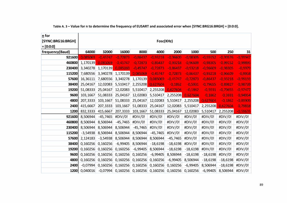
89
Table A. 3 – Value for n to determine the frequency of EUSART and associated error when [SYNC:BRG16:BRGH] = [0:0:0].
n for
[SYNC:BRG16:BRGH]
= [0:0:0]
frequency(Baud) 64000 32000 16000 8000 4000 2000 1000 500 250 31
921600 0,085069 -0,45747 -0,72873 -0,86437 -0,93218 -0,96609 -0,98305 -0,99152 -0,99576 -0,99947
460800 1,170139 0,085069 -0,45747 -0,72873 -0,86437 -0,93218 -0,96609 -0,98305 -0,99152 -0,99895
230400 3,340278 1,170139 0,085069 -0,45747 -0,72873 -0,86437 -0,93218 -0,96609 -0,98305 -0,9979
115200 7,680556 3,340278 1,170139 0,085069 -0,45747 -0,72873 -0,86437 -0,93218 -0,96609 -0,9958
57600 16,36111 7,680556 3,340278 1,170139 0,085069 -0,45747 -0,72873 -0,86437 -0,93218 -0,99159
38400 25,04167 12,02083 5,510417 2,255208 0,627604 -0,1862 -0,5931 -0,79655 -0,89827 -0,98739
19200 51,08333 25,04167 12,02083 5,510417 2,255208 0,627604 -0,1862 -0,5931 -0,79655 -0,97477
9600 103,1667 51,08333 25,04167 12,02083 5,510417 2,255208 0,627604 -0,1862 -0,5931 -0,94954
4800 207,3333 103,1667 51,08333 25,04167 12,02083 5,510417 2,255208 0,627604 -0,1862 -0,89909
2400 415,6667 207,3333 103,1667 51,08333 25,04167 12,02083 5,510417 2,255208 0,627604 -0,79818
1200 832,3333 415,6667 207,3333 103,1667 51,08333 25,04167 12,02083 5,510417 2,255208 -0,59635
921600 8,506944 -45,7465 #DIV/0! #DIV/0! #DIV/0! #DIV/0! #DIV/0! #DIV/0! #DIV/0! #DIV/0!
460800 8,506944 8,506944 -45,7465 #DIV/0! #DIV/0! #DIV/0! #DIV/0! #DIV/0! #DIV/0! #DIV/0!
230400 8,506944 8,506944 8,506944 -45,7465 #DIV/0! #DIV/0! #DIV/0! #DIV/0! #DIV/0! #DIV/0!
115200 -3,54938 8,506944 8,506944 8,506944 -45,7465 #DIV/0! #DIV/0! #DIV/0! #DIV/0! #DIV/0!
57600 2,124183 -3,54938 8,506944 8,506944 8,506944 -45,7465 #DIV/0! #DIV/0! #DIV/0! #DIV/0!
38400 0,160256 0,160256 -6,99405 8,506944 -18,6198 -18,6198 #DIV/0! #DIV/0! #DIV/0! #DIV/0!
19200 0,160256 0,160256 0,160256 -6,99405 8,506944 -18,6198 -18,6198 #DIV/0! #DIV/0! #DIV/0!
9600 0,160256 0,160256 0,160256 0,160256 -6,99405 8,506944 -18,6198 -18,6198 #DIV/0! #DIV/0!
4800 0,160256 0,160256 0,160256 0,160256 0,160256 -6,99405 8,506944 -18,6198 -18,6198 #DIV/0!
2400 -0,07994 0,160256 0,160256 0,160256 0,160256 0,160256 -6,99405 8,506944 -18,6198 #DIV/0!
1200 0,040016 -0,07994 0,160256 0,160256 0,160256 0,160256 0,160256 -6,99405 8,506944 #DIV/0!
Fosc(KHz)

90
Table A. 4 - Value for n to determine the frequency of EUSART and associated error when [SYNC:BRG16:BRGH] = [0:0:1] or [0:1:0].
n for [SYNC:BRG16:BRGH] = [0:0:1] or [0:1:0]
Fosc(kHz)
frequency(Baud) 64000 32000 16000 8000 4000 2000 1000 500 250 31
921600 3,340278 1,170139 0,085069 -0,45747 -0,72873 -0,86437 -0,93218 -0,96609 -0,98305 -0,9979
460800 7,680556 3,340278 1,170139 0,085069 -0,45747 -0,72873 -0,86437 -0,93218 -0,96609 -0,9958
230400 16,36111 7,680556 3,340278 1,170139 0,085069 -0,45747 -0,72873 -0,86437 -0,93218 -0,99159
115200 33,72222 16,36111 7,680556 3,340278 1,170139 0,085069 -0,45747 -0,72873 -0,86437 -0,98318
57600 68,44444 33,72222 16,36111 7,680556 3,340278 1,170139 0,085069 -0,45747 -0,72873 -0,96636
38400 103,1667 51,08333 25,04167 12,02083 5,510417 2,255208 0,627604 -0,1862 -0,5931 -0,94954
19200 207,3333 103,1667 51,08333 25,04167 12,02083 5,510417 2,255208 0,627604 -0,1862 -0,89909
9600 415,6667 207,3333 103,1667 51,08333 25,04167 12,02083 5,510417 2,255208 0,627604 -0,79818
4800 832,3333 415,6667 207,3333 103,1667 51,08333 25,04167 12,02083 5,510417 2,255208 -0,59635
2400 1665,667 832,3333 415,6667 207,3333 103,1667 51,08333 25,04167 12,02083 5,510417 -0,19271
1200 3332,333 1665,667 832,3333 415,6667 207,3333 103,1667 51,08333 25,04167 12,02083 0,614583
921600 8,506944 8,506944 8,506944 -45,7465 #DIV/0! #DIV/0! #DIV/0! #DIV/0! #DIV/0! #DIV/0!
460800 -3,54938 8,506944 8,506944 8,506944 -45,7465 #DIV/0! #DIV/0! #DIV/0! #DIV/0! #DIV/0!
230400 2,124183 -3,54938 8,506944 8,506944 8,506944 -45,7465 #DIV/0! #DIV/0! #DIV/0! #DIV/0!
115200 -0,79365 2,124183 -3,54938 8,506944 8,506944 8,506944 -45,7465 #DIV/0! #DIV/0! #DIV/0!
57600 0,644122 -0,79365 2,124183 -3,54938 8,506944 8,506944 8,506944 -45,7465 #DIV/0! #DIV/0!
38400 0,160256 0,160256 0,160256 0,160256 -6,99405 8,506944 -18,6198 -18,6198 #DIV/0! #DIV/0!
19200 0,160256 0,160256 0,160256 0,160256 0,160256 -6,99405 8,506944 -18,6198 -18,6198 #DIV/0!
9600 -0,07994 0,160256 0,160256 0,160256 0,160256 0,160256 -6,99405 8,506944 -18,6198 #DIV/0!
4800 0,040016 -0,07994 0,160256 0,160256 0,160256 0,160256 0,160256 -6,99405 8,506944 #DIV/0!
2400 -0,02 0,040016 -0,07994 0,160256 0,160256 0,160256 0,160256 0,160256 -6,99405 -19,2708
1200 0,010001 -0,02 0,040016 -0,07994 0,160256 0,160256 0,160256 0,160256 0,160256 -19,2708
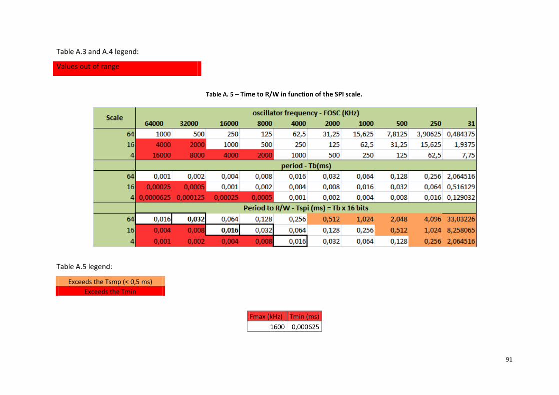
91
Table A.3 and A.4 legend:
Values out of range
Table A. 5 – Time to R/W in function of the SPI scale.
Table A.5 legend:
Exceeds the Tsmp (< 0,5 ms)
Exceeds the Tmin
Fmax (kHz) Tmin (ms)
1600 0,000625

92
Table A. 6 – Time to one bit AD conversion.
FOSC (kHz) 64000 32000 16000 8000 4000 2000 1000 500 250 31
scale ADCON2 register
TAD (ms)
2 0,00003125 0,0000625 0,000125 0,00025 0,0005 0,001 0,002 0,004 0,008 0,064516
4 0,0000625 0,000125 0,00025 0,0005 0,001 0,002 0,004 0,008 0,016 0,129032
8 0,000125 0,00025 0,0005 0,001 0,002 0,004 0,008 0,016 0,032 0,258065
16 0,00025 0,0005 0,001 0,002 0,004 0,008 0,016 0,032 0,064 0,516129
32 0,0005 0,001 0,002 0,004 0,008 0,016 0,032 0,064 0,128 1,032258
64 0,001 0,002 0,004 0,008 0,016 0,032 0,064 0,128 0,256 2,064516
Table A.6 legend:
Recommended values
Limit values
Not feasible

93
Table A. 7 – Total time to ADC process for each acquisition time waiting.
Tadc (ms) 64000 32000 16000 8000 4000 2000 1000 500 250 31
scale ADCON2 register Tacq = 4 Tad
2 0,00053125 0,0010625 0,002125 0,00425 0,0085 0,017 0,034 0,068 0,136 1,096774
4 0,0010625 0,002125 0,00425 0,0085 0,017 0,034 0,068 0,136 0,272 2,193548
8 0,002125 0,00425 0,0085 0,017 0,034 0,068 0,136 0,272 0,544 4,387097
16 0,00425 0,0085 0,017 0,034 0,068 0,136 0,272 0,544 1,088 8,774194
32 0,0085 0,017 0,034 0,068 0,136 0,272 0,544 1,088 2,176 17,54839
64 0,017 0,034 0,068 0,136 0,272 0,544 1,088 2,176 4,352 35,09677
Tacq = 8 Tad
2 0,00065625 0,0013125 0,002625 0,00525 0,0105 0,021 0,042 0,084 0,168 1,354839
4 0,0013125 0,002625 0,00525 0,0105 0,021 0,042 0,084 0,168 0,336 2,709677
8 0,002625 0,00525 0,0105 0,021 0,042 0,084 0,168 0,336 0,672 5,419355
16 0,00525 0,0105 0,021 0,042 0,084 0,168 0,336 0,672 1,344 10,83871
32 0,0105 0,021 0,042 0,084 0,168 0,336 0,672 1,344 2,688 21,67742
64 0,021 0,042 0,084 0,168 0,336 0,672 1,344 2,688 5,376 43,35484

94
Tadc (ms) 64000 32000 16000 8000 4000 2000 1000 500 250 31
Tacq = 16 Tad
2 0,00090625 0,0018125 0,003625 0,00725 0,0145 0,029 0,058 0,116 0,232 1,870968
4 0,0018125 0,003625 0,00725 0,0145 0,029 0,058 0,116 0,232 0,464 3,741935
8 0,003625 0,00725 0,0145 0,029 0,058 0,116 0,232 0,464 0,928 7,483871
16 0,00725 0,0145 0,029 0,058 0,116 0,232 0,464 0,928 1,856 14,96774
32 0,0145 0,029 0,058 0,116 0,232 0,464 0,928 1,856 3,712 29,93548
64 0,029 0,058 0,116 0,232 0,464 0,928 1,856 3,712 7,424 59,87097
Tacq = 0 Tad
2 0,00040625 0,0008125 0,001625 0,00325 0,0065 0,013 0,026 0,052 0,104 0,83871
4 0,0008125 0,001625 0,00325 0,0065 0,013 0,026 0,052 0,104 0,208 1,677419
8 0,001625 0,00325 0,0065 0,013 0,026 0,052 0,104 0,208 0,416 3,354839
16 0,00325 0,0065 0,013 0,026 0,052 0,104 0,208 0,416 0,832 6,709677
32 0,0065 0,013 0,026 0,052 0,104 0,208 0,416 0,832 1,664 13,41935
64 0,013 0,026 0,052 0,104 0,208 0,416 0,832 1,664 3,328 26,83871

95
Tadc (ms) 64000 32000 16000 8000 4000 2000 1000 500 250 31
scale ADCON2 register
Tacq = 2 Tad
2 0,000469 0,000938 0,001875 0,00375 0,0075 0,015 0,03 0,06 0,12 0,967742
4 0,000938 0,001875 0,00375 0,0075 0,015 0,03 0,06 0,12 0,24 1,935484
8 0,001875 0,00375 0,0075 0,015 0,03 0,06 0,12 0,24 0,48 3,870968
16 0,00375 0,0075 0,015 0,03 0,06 0,12 0,24 0,48 0,96 7,741935
32 0,0075 0,015 0,03 0,06 0,12 0,24 0,48 0,96 1,92 15,48387
64 0,015 0,03 0,06 0,12 0,24 0,48 0,96 1,92 3,84 30,96774
Tacq = 6 Tad
2 0,000594 0,001188 0,002375 0,00475 0,0095 0,019 0,038 0,076 0,152 1,225806
4 0,001188 0,002375 0,00475 0,0095 0,019 0,038 0,076 0,152 0,304 2,451613
8 0,002375 0,00475 0,0095 0,019 0,038 0,076 0,152 0,304 0,608 4,903226
16 0,00475 0,0095 0,019 0,038 0,076 0,152 0,304 0,608 1,216 9,806452
32 0,0095 0,019 0,038 0,076 0,152 0,304 0,608 1,216 2,432 19,6129
64 0,019 0,038 0,076 0,152 0,304 0,608 1,216 2,432 4,864 39,22581

96
Tadc (ms) 64000 32000 16000 8000 4000 2000 1000 500 250 31
Tacq = 12 Tad
2 0,000781 0,001563 0,003125 0,00625 0,0125 0,025 0,05 0,1 0,2 1,612903
4 0,001563 0,003125 0,00625 0,0125 0,025 0,05 0,1 0,2 0,4 3,225806
8 0,003125 0,00625 0,0125 0,025 0,05 0,1 0,2 0,4 0,8 6,451613
16 0,00625 0,0125 0,025 0,05 0,1 0,2 0,4 0,8 1,6 12,90323
32 0,0125 0,025 0,05 0,1 0,2 0,4 0,8 1,6 3,2 25,80645
64 0,025 0,05 0,1 0,2 0,4 0,8 1,6 3,2 6,4 51,6129
Tacq = 20 Tad
2 0,001031 0,002063 0,004125 0,00825 0,0165 0,033 0,066 0,132 0,264 2,129032
4 0,002063 0,004125 0,00825 0,0165 0,033 0,066 0,132 0,264 0,528 4,258065
8 0,004125 0,00825 0,0165 0,033 0,066 0,132 0,264 0,528 1,056 8,516129
16 0,00825 0,0165 0,033 0,066 0,132 0,264 0,528 1,056 2,112 17,03226
32 0,0165 0,033 0,066 0,132 0,264 0,528 1,056 2,112 4,224 34,06452
64 0,033 0,066 0,132 0,264 0,528 1,056 2,112 4,224 8,448 68,12903
Tacq < 140 ns
Tadc > 0.5 ms
Tacq < 2 Tad

97
Table A. 8 – Minor time got to execute a sampling and sending cycle.
Fosc Minor Tadc (ms) Minor Tsending (ms) Minor Tspi (ms) Tsmp (ms)
64 MHz 0,003125 0,0109132 0,016 0,0409514
32 MHz 0,003125 0,0109757 0,032 0,0570764
Table A. 9 – Time to sample relating the number of channels to the number of samplings.
Tsmp (ms) Sample amount
channels amount 2 4 6 8 10 12 14 16 18 20 24 28
2 0,5 0,25 0,166667 0,125 0,1 0,083333 0,071429 0,0625 0,055556 0,05 0,041667 0,035714
3 0,333333 0,166667 0,111111 0,083333 0,066667 0,055556 0,047619 0,041667 0,037037 0,033333 0,027778 0,02381
4 0,25 0,125 0,083333 0,0625 0,05 0,041667 0,035714 0,03125 0,027778 0,025 0,020833 0,017857
5 0,2 0,1 0,066667 0,05 0,04 0,033333 0,028571 0,025 0,022222 0,02 0,016667 0,014286
6 0,166667 0,083333 0,055556 0,041667 0,033333 0,027778 0,02381 0,020833 0,018519 0,016667 0,013889 0,011905
7 0,142857 0,071429 0,047619 0,035714 0,028571 0,02381 0,020408 0,017857 0,015873 0,014286 0,011905 0,010204
8 0,125 0,0625 0,041667 0,03125 0,025 0,020833 0,017857 0,015625 0,013889 0,0125 0,010417 0,008929
9 0,111111 0,055556 0,037037 0,027778 0,022222 0,018519 0,015873 0,013889 0,012346 0,011111 0,009259 0,007937
10 0,1 0,05 0,033333 0,025 0,02 0,016667 0,014286 0,0125 0,011111 0,01 0,008333 0,007143
11 0,090909 0,045455 0,030303 0,022727 0,018182 0,015152 0,012987 0,011364 0,010101 0,009091 0,007576 0,006494
12 0,0833 0,041667 0,027778 0,020833 0,016667 0,013889 0,011905 0,010417 0,009259 0,0083 0,006944 0,005952
13 0,076923 0,038462 0,025641 0,019231 0,015385 0,012821 0,010989 0,009615 0,008547 0,007692 0,00641 0,005495
14 0,071429 0,035714 0,02381 0,017857 0,014286 0,011905 0,010204 0,008929 0,007937 0,007143 0,005952 0,005102
15 0,066667 0,033333 0,022222 0,016667 0,013333 0,011111 0,009524 0,008333 0,007407 0,006667 0,005556 0,004762
16 0,0625 0,03125 0,020833 0,015625 0,0125 0,010417 0,008929 0,007813 0,006944 0,0063 0,005208 0,004464

98
Table A.9 was computed using the equation: TSMP = 1 / (0.5 × nºch × nºsamples)
Table A.9 legend
Lower than the possible max sending rate (Table A.8)
Lower than the TSPI
Unfeasible without buffer for F< 921600
Table A.10 was computed using the equation: t = 65535 × scale × (1 / FOSC/4)
Table A. 10 – Time counted regarding the frequency and the timer scale.
tmr1 & tmr3 (2 bytes) count:
65535
maximum time allowed FOSC/4 (ms)
16000 8000 4000 2000 1000 500 250 125 62,5 7,75
8 32,7675 65,535 131,07 262,14 524,28 1048,56 2097,12 4194,24 8388,48 67649,03
4 16,38375 32,7675 65,535 131,07 262,14 524,28 1048,56 2097,12 4194,24 33824,52
2 8,191875 16,38375 32,7675 65,535 131,07 262,14 524,28 1048,56 2097,12 16912,26
1 4,0959375 8,191875 16,38375 32,7675 65,535 131,07 262,14 524,28 1048,56 8456,129

99
Annex B - Schematic


101
Annex C – Programming Codes
The Annex C is presented in a written part, containing the code of the firmware, and a
digital part containing the codes of the firmware and the software as well the executable
generated.
#include<p18f14k22.h> #include<spi.h> //#include<usart.h> //#define _SS1 PORTCbits.RC4 //#define _SS2 PORTCbits.RC3 //#define _SS3 PORTCbits.RCx #define _CH1 0x09 #define _CH2 0x11 unsigned char _Rcpt_Con;// _count_time = 0x00; volatile unsigned char _SS_CH[] = 0b11101111,0b11110111; static unsigned char _adsRS = 4, _comut_SS = 0;// i=0; void _int_High_Handler(); void _int_Low_Handler(); /**************************** configuration bits *****************************/ #pragma config FOSC = IRC, PLLEN = OFF, PCLKEN = OFF, FCMEN = OFF, IESO = OFF #pragma config PWRTEN = OFF, BOREN = OFF, BORV = 30 #pragma config WDTEN = OFF, WDTPS = 32768 #pragma config MCLRE = ON, HFOFST = OFF #pragma config STVREN = OFF, BBSIZ = ON, LVP = OFF, XINST = OFF #pragma config CP0 = OFF, CP1 = OFF #pragma config CPB = OFF, CPD = OFF #pragma config WRT0 = OFF, WRT1 = OFF #pragma config WRTB = OFF, WRTC = OFF, WRTD = OFF #pragma config EBTR0 = OFF, EBTR1 = OFF #pragma config EBTRB = OFF /*************************** pre processing code *****************************/ /// high priority irq #pragma code high_vector = 0x0008 void high_vector(void) _asm GOTO _int_High_Handler _endasm #pragma code /// high priority irs #pragma interrupt _int_High_Handler

102
void _int_High_Handler() // PORTAbits.RA5 = ~PORTAbits.RA5; if(PIR1bits.CCP1IF) // PORTAbits.RA5 = ~PORTAbits.RA5; // PIR2bits.TMR3IF = 0; PIR1bits.ADIF = 0; // ADC Interrupt Flag (R/W) PIR1bits.CCP1IF = 0; // CCP Interrupt Flag (R/W) TXREG = ADRESH; // puts the content of ADRESH register as char on output register while (!PIR1bits.TXIF); PIR1bits.ADIF = 0; // ADC Interrupt Flag (R/W) if(ADCON0 == _CH1) // commutates the ADC channel ADCON0 = _CH2; else ADCON0 = _CH1; if (_adsRS == 10 || _adsRS == 4) _adsRS = 4; // first address _comut_SS = ++_comut_SS & 1; // commutates the index PORTC &= _SS_CH[_comut_SS]; // enables SS // PORTCbits.RC4 =~ PORTCbits.RC4; // PORTCbits.RC3 =~ PORTCbits.RC3; WriteSPI(_adsRS<<2); // indicate the address to be read while(!DataRdySPI()); // ensure the read to be completed TXREG = ReadSPI() | 1<<_comut_SS; // read a byte to variable Val_SPI PORTC |= 0b00011000; // disables SS _adsRS++; // goes to the next address else PORTC &= _SS_CH[_comut_SS]; WriteSPI(_adsRS<<2); // indicate the address to be read while(!DataRdySPI()); // ensure the read to be completed TXREG = ReadSPI(); // read a byte to variable Val_SPI PORTC |= 0b00011000; // disables SS _adsRS++; // goes to the next address // PORTAbits.RA5 = ~PORTAbits.RA5; /// low priority irq #pragma code low_vector = 0x0018 void low_vector(void) _asm GOTO _int_Low_Handler _endasm

103
#pragma code /// low priority irs #pragma interruptlow _int_Low_Handler void _int_Low_Handler() if(PIR1bits.RCIF) // PORTAbits.RA5 = ~PORTAbits.RA5; _Rcpt_Con = RCREG; // Receives an incoming byte while (!PIR1bits.RCIF); // wait for complete reading _adsRS = 4; // initializes the accel address _comut_SS = 0; // initializes the SS pin // _count_time = 1; // PIR2bits.TMR3IF = 0; T3CONbits.TMR3ON =~ T3CONbits.TMR3ON; // turn on/off the timer // VREFCON1bits.D1EN =~ VREFCON1bits.D1EN; void main(void) /******************* initializations ******************/ TRISBbits.TRISB6 = 0; // SCK output TRISCbits.TRISC6 = 1; // SS disable // SS3 output - to be addressed TRISCbits.TRISC4 = 0; // SS2 output - (ST) TRISCbits.TRISC3 = 0; // SS1 output - (ST) // TRISCbits.TRISC2 = 0; // SSx output - (ST) TRISAbits.TRISA5 = 0; // SS_SDCard output - (TTL) TRISCbits.TRISC7 = 0; // MOSI output TRISBbits.TRISB4 = 1; // MISO input PORTC |= 0b00011000; // Set all SS disabled TRISBbits.TRISB5 = 1; // USART input -- this need to be configured as input -- !!! TRISBbits.TRISB7 = 0; // USART output TRISAbits.TRISA2 = 1; // AN2 input TRISCbits.TRISC0 = 1; // AN4 input TRISCbits.TRISC5 = 0; // CCP1 output // ANSELbits.ANS6 = 0; ANSELHbits.ANS11 = 0; // disable the analog function and enable USART function ANSELHbits.ANS10 = 0; // disable the analog function and enable SPI function ANSELbits.ANS7 = 0; // disable the analog function and enable SPI function ANSELbits.ANS2 = 1; // configure as analog input ANSELHbits.ANS8 = 1; // configure as analog input // _SS1 = 1; // _SS2 = 1; // _SS3 = 1; // _SS_SDCARD = 1;

104
// PORTAbits.RA5 = 1; // PORTCbits.RC6 = 1; // PORTCbits.RC4 = 1; // PORTCbits.RC3 = 1; /*************************** Set up oscillator **********************/ OSCTUNE &= 0x80; // Oscillator, module works at factory calibrated frequency and with 16MHz HFINTOSC reference source // OSCTUNEbits.PLLEN = 1; // enables the 4xPLL = 64MHz / 32MHz -- 139->115200 (limit of 127) OSCCON |= 0b11110010; // define the frequency in 16MHz -- 34->115200; 103->34800 -- 0b11110110 - sleep instruction enter in idle mode // OSCCON |= 0b11100000; // define the frequency in 8MHz -- 0b11100010 - sleep instruction enter in idle mode // OSCCON &= 0b11101111; // OSCCON |= 0b11010000; // define the frequency in 4MHz -- 0b11010010 - sleep instruction enter in idle mode // OSCCON &= 0b11011111; // OSCCON &= 0b11001111; // define the frequency in 2MHz -- 0b11000010 - sleep instruction enter in idle mode // OSCCON |= 0b11000000; /************************ Global interrupt ************************/ RCONbits.IPEN = 1; // Enables the usage of priority levels on interrupts // INTCONbits.GIE = 1; // Enables all interrupts INTCONbits.GIEH = 1; // Enables all interrupts == GIE // INTCONbits.PEIE = 1; // Enables all peripherals interrupts INTCONbits.GIEL = 1; // Enables all peripherals interrupts == PEIE /*************************** USART ***********************/ SPBRG = 0x22; SPBRGH = 0x22 >> 8; // Initialize the SPBRGH:SPBRG with 34 decimal value: FOSC = 16MHz and Baud Rate = 115,2 KHz (pg. 191) // SPBRG = 0x01; // SPBRGH = 0x01 >> 8; // Initialize the SPBRGH:SPBRG with 1 decimal value: FOSC = 32MHz and Baud Rate = 921,6 KHz (pg. 191) // SPBRG = 0x03; // SPBRGH = 0x03 >> 8; // Initialize the SPBRGH:SPBRG with 3 decimal value: FOSC = 64MHz and Baud Rate = 921,6 KHz (pg. 191) // SPBRG = 0x1F; // SPBRGH = 0x1F >> 8; // Initialize the SPBRGH:SPBRG with 31 decimal value: FOSC = 16MHz and Baud Rate = 128 KHz (pg. 191) TXSTA = 0x26; // TX is actually enabled, Asynchronous mode, 8 bits, BRGH in High speed RCSTA = 0x90; // RX is continuously enabled, 8 bits rcpt, receives continuously BAUDCON = 0x4A; // * Auto baud detection disabled, Wake-up event on reception enabled, Baud Rate Generator in 16 bits mode PIE1bits.RCIE = 1; // enables interrupts on reception

105
IPR1bits.RCIP = 0; // EUSART RX Interrupt high priority PIE1bits.TXIE = 0; // EUSART TX Interrupt disabled IPR1bits.TXIP = 0; // EUSART TX Interrupt low priority /**************************** SPI ****************************/ SSPSTATbits.SMP = 0; // the data is sampled at middle SSPSTATbits.CKE = 1; // transmission occurs on transition from active to idle clock state // SSPCON1 = 0x02; // no collision, no overflow, idle at low level, clk = FOSC/64 SSPCON1 = 0x01; // no collision, no overflow, idle at low level, clk = FOSC/16 // SSPCON1 = 0x00; // no collision, no overflow, idle at low level, clk = FOSC/4 SSPCON1bits.SSPEN = 1; // Enables SPI PIE1bits.SSPIE = 0; // disables (external) SPI Interrupt IPR1bits.SSPIP = 0; // SPI Interrupt low priority /***************************** ADC **************************/ // VREFCON0 = 0xD0; // It set and enable this register to works with Fixed Reference Voltage of 1,024 V // while(VREFCON0bits.FVR1ST); // Wait the internal reference stabilization // VREFCON1 = 0x60; // Enables internal voltage reference and disables output reference VREFCON1 = 0x44; // Disables internal voltage reference and disables output reference VREFCON2 = 0XFF; // Vref = Vsource // ADCON1 = 0x00; // Positive reference as internal (Vdd) and negative reference as Vss - configure VREFCON1 ADCON1 = 0x04; // Positive reference as external (Vref) and negative reference as Vss - configure VREFCON1 // ADCON1 = 0x08; // Positive reference as internal (FVR) and negative reference as Vss - configure VREFCON0 // ADCON2 = 0x0D; // Configure the register ADRES as left justified, TAD multiplied by 2 and the clock as FOSC/16 -> 0x0D / 0x0E -> FOSC/64 ADCON2 = 0x2C; // FOSC/4, 12 TAD, left justified. ADCON0 = _CH1; // determines the channel and active ADON bits to star conversion ADCON0bits.ADON = 1; // Enable ADC // --- !!! Uncomment the ANSEL and TRIS register in initializations !!! --- PIE1bits.ADIE = 0; // ADC Interrupt enable IPR1bits.ADIP = 0; // ADC Interrupt as high priority /***************************** CCPM1 **************************/ CCP1CON = 0x0B; // Compare mode with a special event trigger // CCPR1H = 0x00; // Value to be compared --- !!! does not work properly at this sampling frequency !!! --- // CCPR1L = 0xC8; // = 12,5 us / 50 us --- !!! not feasible with serial port! excides the sampling time !!! --- // CCPR1H = 0x01; // Value to be compared --- !!! overflow at 25s !!! --- // CCPR1L = 0x90; // = 200 us

106
// CCPR1H = 0x03; // Value to be compared --- !!! overflow at 30s !!! --- // CCPR1L = 0x20; // = 400 us // CCPR1H = 0x00; // Value to be compared --- !!! !!! --- // CCPR1L = 0x7D; // = 125 us // CCPR1H = 0x01; // Value to be compared --- // CCPR1L = 0xF4; // = 250 us CCPR1H = 0x03; // Value to be compared --- CCPR1L = 0xE8; // = 500 us // CCPR1H = 0x07; // Value to be compared --- // CCPR1L = 0xD0; // = 1000 us PIR1bits.CCP1IF = 0; // CCP Interrupt Flag (R/W) PIE1bits.CCP1IE = 1; // CCP Interrupt disabled IPR1bits.CCP1IP = 1; // CCP Interrupt priority /*************************** Timer3 ***************************/ T3CON = 0b10011100; // operation with 16 bits, prescale 1:2, TMR3 as clk for CCP, IRC, actually off // TMR3L = ; // NOT USED !!! // TMR3H = ; // NOT USED !!! PIR2bits.TMR3IF = 0; // TIMER3 Interrupt Flag (R/W) PIE2bits.TMR3IE = 0; // TIMER3 Interrupt enable IPR2bits.TMR3IP = 0; // TIMER3 Interrupt priority /******************************************************************************/ /**/ while(1) Sleep();