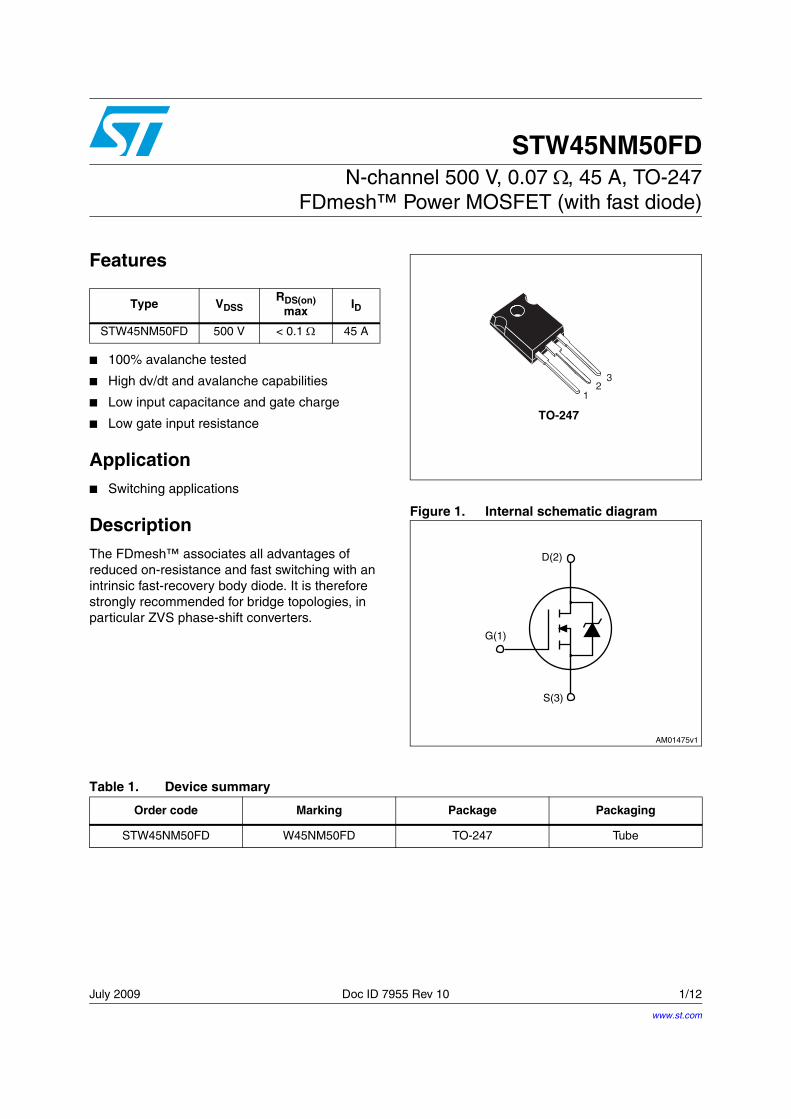
n-channel 500 v, 0.07 , 45 a, to-247 fdmesh power mosfet
TRANSCRIPT
July 2009 Doc ID 7955 Rev 10 1/12
12
STW45NM50FDN-channel 500 V, 0.07 Ω, 45 A, TO-247
FDmesh™ Power MOSFET (with fast diode)
Features
100% avalanche tested
High dv/dt and avalanche capabilities
Low input capacitance and gate charge
Low gate input resistance
Application Switching applications
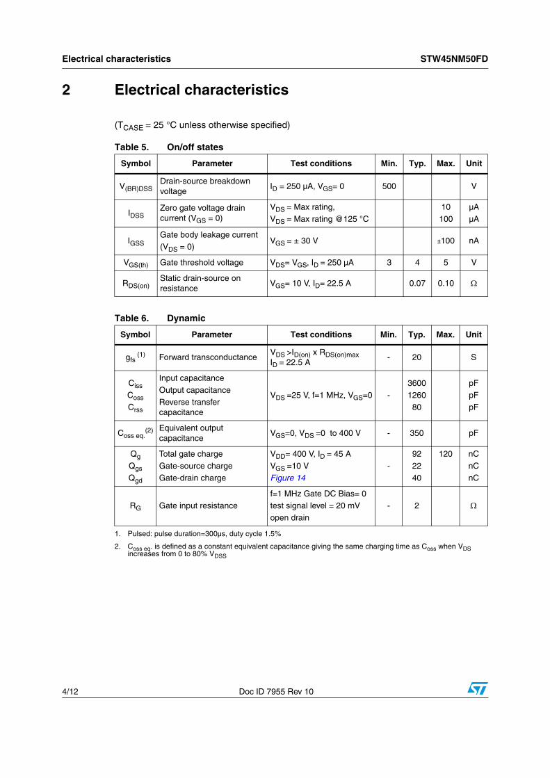
DescriptionThe FDmesh™ associates all advantages of reduced on-resistance and fast switching with an intrinsic fast-recovery body diode. It is therefore strongly recommended for bridge topologies, in particular ZVS phase-shift converters.
Figure 1. Internal schematic diagram
Type VDSSRDS(on)
max ID
STW45NM50FD 500 V < 0.1 Ω 45 A
TO-247
12
3
Table 1. Device summary
Order code Marking Package Packaging
STW45NM50FD W45NM50FD TO-247 Tube
www.st.com
Contents STW45NM50FD
2/12 Doc ID 7955 Rev 10
Contents
1 Electrical ratings . . . . . . . . . . . . . . . . . . . . . . . . . . . . . . . . . . . . . . . . . . . . 3
2 Electrical characteristics . . . . . . . . . . . . . . . . . . . . . . . . . . . . . . . . . . . . . 42.1 Electrical characteristics (curves) . . . . . . . . . . . . . . . . . . . . . . . . . . . . . 6
3 Test circuits . . . . . . . . . . . . . . . . . . . . . . . . . . . . . . . . . . . . . . . . . . . . . . 8
4 Package mechanical data . . . . . . . . . . . . . . . . . . . . . . . . . . . . . . . . . . . . . 9
5 Revision history . . . . . . . . . . . . . . . . . . . . . . . . . . . . . . . . . . . . . . . . . . . 11

STW45NM50FD Electrical ratings
Doc ID 7955 Rev 10 3/12
1 Electrical ratings
Table 2. Absolute maximum ratings
Symbol Parameter Value Unit
VDS Drain-source voltage (VGS = 0) 500 V
VGS Gate-source voltage ± 30 V
ID Drain current (continuous) at TC = 25 °C 45 A
ID Drain current (continuous) at TC=100 °C 28.4 A
IDM(1)
1. Pulse width limited by safe operating area
Drain current (pulsed) 180 A
PTOT Total dissipation at TC = 25 °C 417 W
Derating factor 2.08 W/°C
dv/dt(2)
2. ISD ≤ 45 A, di/dt ≤ 400 A/µs, VDD = 80%V(BR)DSS
Peak diode recovery voltage slope 20 V/ns
TJ
Tstg
Operating junction temperature
Storage temperature-65 to 150 °C
Table 3. Thermal resistance
Symbol Parameter Value Unit
Rthj-case Thermal resistance junction-case max 0.3 °C/W
Rthj-a Thermal resistance junction-ambient max 30 °C/W
Tl Maximum lead temperature for soldering purpose 300 °C
Table 4. Avalanche data
Symbol Parameter Value Unit
IARAvalanche current, repetitive or not-repetitive
(pulse width limited by Tj max)22.5 A
EASSingle pulse avalanche energy
(starting TJ = 25 °C, ID = IAR, VDD = 50 V)800 mJ
Electrical characteristics STW45NM50FD
4/12 Doc ID 7955 Rev 10
2 Electrical characteristics
(TCASE = 25 °C unless otherwise specified)
Table 5. On/off states
Symbol Parameter Test conditions Min. Typ. Max. Unit
V(BR)DSSDrain-source breakdown voltage
ID = 250 µA, VGS= 0 500 V
IDSSZero gate voltage drain current (VGS = 0)
VDS = Max rating,VDS = Max rating @125 °C
10100
µAµA
IGSSGate body leakage current(VDS = 0)
VGS = ± 30 V ±100 nA
VGS(th) Gate threshold voltage VDS= VGS, ID = 250 µA 3 4 5 V
RDS(on)Static drain-source on resistance
VGS= 10 V, ID= 22.5 A 0.07 0.10 Ω
Table 6. Dynamic
Symbol Parameter Test conditions Min. Typ. Max. Unit
gfs (1)
1. Pulsed: pulse duration=300µs, duty cycle 1.5%
Forward transconductanceVDS >ID(on) x RDS(on)max ID = 22.5 A
- 20 S
Ciss
Coss
Crss
Input capacitance
Output capacitance
Reverse transfer capacitance
VDS =25 V, f=1 MHz, VGS=0 -
3600
126080
pF
pFpF
Coss eq.(2)
2. Coss eq. is defined as a constant equivalent capacitance giving the same charging time as Coss when VDS increases from 0 to 80% VDSS
Equivalent output capacitance
VGS=0, VDS =0 to 400 V - 350 pF
Qg
Qgs
Qgd
Total gate charge
Gate-source chargeGate-drain charge
VDD= 400 V, ID = 45 A
VGS =10 VFigure 14
-
92
2240
120 nC
nCnC
RG Gate input resistancef=1 MHz Gate DC Bias= 0test signal level = 20 mV
open drain
- 2 Ω

STW45NM50FD Electrical characteristics
Doc ID 7955 Rev 10 5/12
Table 7. Switching times
Symbol Parameter Test conditions Min. Typ. Max. Unit
td(on)
tr
Turn-on delay time
Rise time
VDD=250 V, ID= 22.5 A, RG=4.7 Ω, VGS=10 V
Figure 15
-26.5
107.5-
ns
ns
tr(Voff)
tftc
Off-voltage rise time
Fall time
Cross-over time
VDD=400 V, ID= 45 A,
RG=4.7 Ω, VGS=10 V
Figure 15
-
21.6
87.7
110.9
-
ns
ns
ns
Table 8. Source drain diode
Symbol Parameter Test conditions Min. Typ. Max. Unit
ISD Source-drain current - 45 A
ISDM(1)
1. Pulse width limited by safe operating area
Source-drain current (pulsed) - 180 A
VSD(2)
2. Pulsed: pulse duration=300µs, duty cycle 1.5%
Forward on voltage ISD = 45 A, VGS = 0 - 1.5 V
trrQrr
IRRM
Reverse recovery time
Reverse recovery chargeReverse recovery current
ISD = 45 A, VDD = 100 Vdi/dt = 100 A/µs,(see Figure 18)
-
200
160016
ns
nCA
trrQrr
IRRM
Reverse recovery timeReverse recovery charge
Reverse recovery current
ISD= 45 A, Tj = 150 °Cdi/dt = 100 A/µs,
VDD=100 V, (see Figure 18)
-324
4017
24.8
nsnC
A

Electrical characteristics STW45NM50FD
6/12 Doc ID 7955 Rev 10
2.1 Electrical characteristics (curves) Figure 2. Safe operating area Figure 3. Thermal impedance
Figure 4. Output characteristics Figure 5. Transfer characteristics
Figure 6. Transconductance Figure 7. Static drain-source on resistance
STW45NM50FD Electrical characteristics
Doc ID 7955 Rev 10 7/12
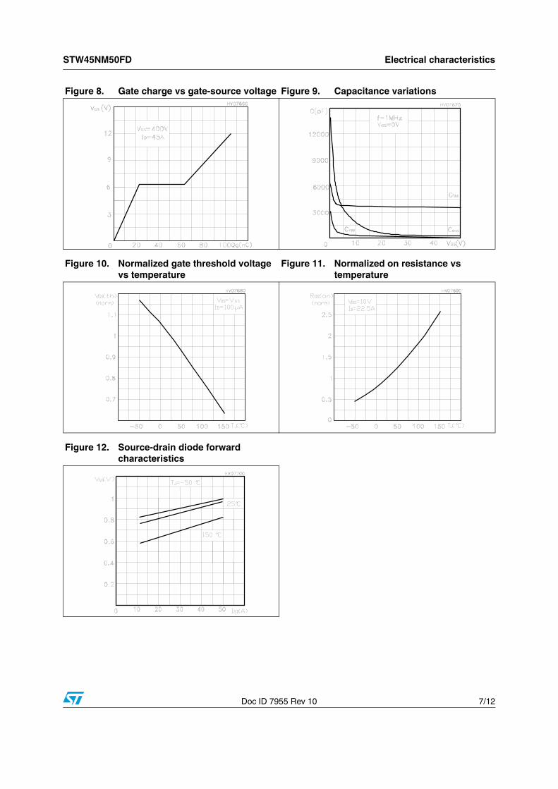
Figure 8. Gate charge vs gate-source voltage Figure 9. Capacitance variations
Figure 10. Normalized gate threshold voltage vs temperature
Figure 11. Normalized on resistance vs temperature
Figure 12. Source-drain diode forward characteristics

Test circuits STW45NM50FD
8/12 Doc ID 7955 Rev 10
3 Test circuits
Figure 13. Switching times test circuit for resistive load
Figure 14. Gate charge test circuit
Figure 15. Test circuit for inductive load switching and diode recovery times
Figure 16. Unclamped inductive load test circuit
Figure 17. Unclamped inductive waveform Figure 18. Switching time waveform
AM01468v1
VGS
PW
VD
RG
RL
D.U.T.
2200
µF3.3µF
VDD
AM01469v1
VDD
47kΩ 1kΩ
47kΩ
2.7kΩ
1kΩ
12V
Vi=20V=VGMAX
2200µF
PW
IG=CONST100Ω
100nF
D.U.T.
VG
AM01470v1
AD
D.U.T.
SB
G
25 Ω
A A
BB
RG
G
FASTDIODE
D
S
L=100µH
µF3.3 1000
µF VDD
AM01471v1
Vi
Pw
VD
ID
D.U.T.
L
2200µF
3.3µF VDD
AM01472v1
V(BR)DSS
VDDVDD
VD
IDM
ID
AM01473v1
VDS
ton
tdon tdoff
toff
tftr
90%
10%
10%
0
0
90%
90%
10%
VGS

STW45NM50FD Package mechanical data
Doc ID 7955 Rev 10 9/12
4 Package mechanical data
In order to meet environmental requirements, ST offers these devices in different grades of ECOPACK® packages, depending on their level of environmental compliance. ECOPACK® specifications, grade definitions and product status are available at: www.st.com. ECOPACK is an ST trademark.

Package mechanical data STW45NM50FD
10/12 Doc ID 7955 Rev 10
Dim. mm.
Min. Typ Max.51.558.4A
06.202.21A
04.10.1b
04.20.21b
04.30.32b
08.004.0c
51.0258.91D
57.5154.51E
54.5e
08.4102.41L
03.407.31L
05.812L
56.355.3Pø
05.505.4Rø
05.5S
TO-247 Mechanical data

STW45NM50FD Revision history
Doc ID 7955 Rev 10 11/12
5 Revision history
Table 9. Document revision history
Date Revision Changes
05-Apr-2005 8 Modified value on Source drain diode
26-Apr-2006 9 New template
23-Jul-2009 10 Modified values on Switching times

STW45NM50FD
12/12 Doc ID 7955 Rev 10
Please Read Carefully:
Information in this document is provided solely in connection with ST products. STMicroelectronics NV and its subsidiaries (“ST”) reserve theright to make changes, corrections, modifications or improvements, to this document, and the products and services described herein at anytime, without notice.
All ST products are sold pursuant to ST’s terms and conditions of sale.
Purchasers are solely responsible for the choice, selection and use of the ST products and services described herein, and ST assumes noliability whatsoever relating to the choice, selection or use of the ST products and services described herein.
No license, express or implied, by estoppel or otherwise, to any intellectual property rights is granted under this document. If any part of thisdocument refers to any third party products or services it shall not be deemed a license grant by ST for the use of such third party productsor services, or any intellectual property contained therein or considered as a warranty covering the use in any manner whatsoever of suchthird party products or services or any intellectual property contained therein.
UNLESS OTHERWISE SET FORTH IN ST’S TERMS AND CONDITIONS OF SALE ST DISCLAIMS ANY EXPRESS OR IMPLIEDWARRANTY WITH RESPECT TO THE USE AND/OR SALE OF ST PRODUCTS INCLUDING WITHOUT LIMITATION IMPLIEDWARRANTIES OF MERCHANTABILITY, FITNESS FOR A PARTICULAR PURPOSE (AND THEIR EQUIVALENTS UNDER THE LAWSOF ANY JURISDICTION), OR INFRINGEMENT OF ANY PATENT, COPYRIGHT OR OTHER INTELLECTUAL PROPERTY RIGHT.
UNLESS EXPRESSLY APPROVED IN WRITING BY AN AUTHORIZED ST REPRESENTATIVE, ST PRODUCTS ARE NOTRECOMMENDED, AUTHORIZED OR WARRANTED FOR USE IN MILITARY, AIR CRAFT, SPACE, LIFE SAVING, OR LIFE SUSTAININGAPPLICATIONS, NOR IN PRODUCTS OR SYSTEMS WHERE FAILURE OR MALFUNCTION MAY RESULT IN PERSONAL INJURY,DEATH, OR SEVERE PROPERTY OR ENVIRONMENTAL DAMAGE. ST PRODUCTS WHICH ARE NOT SPECIFIED AS "AUTOMOTIVEGRADE" MAY ONLY BE USED IN AUTOMOTIVE APPLICATIONS AT USER’S OWN RISK.
Resale of ST products with provisions different from the statements and/or technical features set forth in this document shall immediately voidany warranty granted by ST for the ST product or service described herein and shall not create or extend in any manner whatsoever, anyliability of ST.
ST and the ST logo are trademarks or registered trademarks of ST in various countries.
Information in this document supersedes and replaces all information previously supplied.
The ST logo is a registered trademark of STMicroelectronics. All other names are the property of their respective owners.
© 2009 STMicroelectronics - All rights reserved
STMicroelectronics group of companies
Australia - Belgium - Brazil - Canada - China - Czech Republic - Finland - France - Germany - Hong Kong - India - Israel - Italy - Japan - Malaysia - Malta - Morocco - Philippines - Singapore - Spain - Sweden - Switzerland - United Kingdom - United States of America
www.st.com