n i t a l t di it lnyquist analog to digital ctconverters · n i t a l t di it lnyquist analog to...
TRANSCRIPT

1
N i t A l t Di it l C tNyquist Analog to Digital ConvertersTuesday, March 1st, 9:15 – 11:00
Snorre Aunet ([email protected])
Nanoelectronics group
Department of Informatics
University of Oslo
February the 22th• 3.1 Introduction
• 3.1.1 DAC applications
• 3.1.2 Voltage and currentreferences
• 3.2 Types of converters
3.4 Capacitor basedarchitectures3.4.1 Capacitive divider DAC3.4.2 Capacitive MDAC3.4.3 ”Flip around” MDAC3.4.4 Hybrid capacitive
• 3.3 Resistor basedarchitectures
• 3.3.1 Resistive divider
• 3.3.2 X-Y selection
• 3.3.3 Settling of the output voltage
• 3.3.4 Segmentedarchitectures
y presistive DACs3.5 Current source basedarchitectures3.5.1 Basic operation3.5.2 Unity current generator3.5.3 Random mismatch withunary selection3.5.4. Current sourcesselection
• 3.3.5 Effects of mismatch
• 3.3.6 Trimming and calibration
• 3.3.7 Digital Potentiometer
• 3.3.8 R-2R Resistor Ladder DAC
• 3.3.9 Deglitching
21. mars 2011
selection3.5.5 Current switching and segmentation3.5.6 Switching of currentsources3.6 Other architectures(The contents refer to ”Maloberti”)

2
March the 1st
• Contents of Chapter 4:
• 4.1 Introduction
• 4.2 Timing accuracy
• 4.3 Full flash converters
• 4.4 Sub-ranging and two-stepconverters
• 4.5 Folding and interpolation
• 4.6 Time interleaved converters
• 4 7 Successive approximation• 4.7 Successive approximationconverter
• 4.8 Pipeline converters
• 4.9 Other architectures
31. mars 2011
ADCs and throughput (1 of 2)
• Depending onthe bandwidth ofthe input signalthe input signal, ADCs may useone or multiple clock cycles per conversion.

3
ADCs and throughput ( 2 of 2)
• Depending on the bandwidth of the input signal, ADCsmay use one or multiple clock cycles per conversion.
Full Flash Converters • Compare input with all
transition points betweenadjacent quantizationintervals - ”brute force”
• Quick – 1 CP, ”flash”.
• n bit: 2n-1 reference voltagesand comparators.
• ”1” output up to a certainlevel, ”0” over: thermometercode.
O• ROM decoder.
• Quantization step ∆= (Vref+ -Vref+)/ 2n-1 , with first and last step equal to ∆/2.

4
Successive approx ADC algorithm• If we have weights of 1
kg, 2 kg, 4 kg, 8 kg, 16 kg 32 kg and will findkg, 32 kg and will find the weight of an unknown X assumed to be 45 kg.
• 1011012
=1*32+0*16+1*8+1*4+0*2+1*1
= 4510
Successive approximation converter (ch. 4.5.4)
• Multiple clock periods
• Exploits knowledge ofpreviously determined bits to yfind next significant bit.
• Low complexity and lowpower consumption
• For a given dynamic range 0 – VFS the MSB distinguishesbetween input signals belowor above VFS / 2. Comparingthe input with VFS / 2 obtainsthe first bit as seen in Fig. 4.28 a)
• Fig. 4.29 shows a typicalblock diagram.

5
Successive approximation converter (ch. 4.5.4)
• For a given dynamic range 0 –VFS the MSB distinguishesbetween input signals below or above VFS / 2. Comparing theinput with VFS / 2 obtains thefirst bit as seen in Fig. 4.28 a)
• The knowledge of the MSB restricts the search for the nextbit to either the upper or lowerhalf of the 0 to VFS interval. Threshold for second bit is VFS / 2 or 3VFS / 4 (the case here).
• After this the next bit is chosenand next bit can be estimated .
• The timing diagram (upper left) describes the case for three bits.
• Voltages for comparisons aregenerated by a DAC under control of the SAR register.
Successive approximation converter (ch. 4.5.4)
• Timing diagram: S/H samples the input during the 1st clock period and holds it for N successive clock intervals.
• The DAC is controlled by the SAR algorithm (Fig 4 28 b))• The DAC is controlled by the SAR algorithm (Fig. 4.28 b))
• Initially the SAR sets MSB to 1 as a prediction, though this may be changed to 0.
• The process continues until all n bits have been determined.
• As the start of the next conversion (while the S&H is sampling the next input, theSAR provides the n-bit output and resets the registers.
• The name of the algorithm comes from the fact that the voltage from the DAC is an improving approximation of the sampled input voltage.

6
Succ. Approx ADC, example 13.2 in J&M
Sub-ranging and Two-step converters • Sub-ranging and two-step ADCs
have better speed-accuracytradeoff than full flash for n>8.
• 2 (or 3) clock periods per conversion but smaller number ofconversion, but smaller number ofcomparators and thus benefittingsilicon area, power consumptionand capacitive loading of the S/H.
• The DAC converts the M MSBsback to an analog signal that is subtracted from the held input thatis converted to digital by the 2nd N-bit flash that yields the LSBsbit flash that yields the LSBs.
• Digital Logic combine coarse and fine bits to obtain the n = (M+N) bit output.
• Subranging ADCs does not have the amplification by K (two-stephas).

7
Sub-ranging and Two-step converters • Fig. 4.10 shows the timing
diagram.
• Four logic signals (below mainclock signal) are derived from themain clockmain clock.
• Assuming half a clock period is used to provide each function or group of functions means that 2 clock periods are enough for 1 conversion.
• For an 8 bit conversion: M = N = 4 2(16-1) = 30 comparators are
d d i t d f 255 f 8 bitneeded, instead of 255 for an 8-bit flash ADC.
• The spared area and power aremuch more than what is needed for the DAC and residue generator.
• S/H is only loaded by 2M comp.
Folding and interpolation
• Splits the input range into a number of sectors
• Single folding bends the input d ½ V d i iaround ½ VFS and gives rise to
2 sectors (1-bit) with peakamplitude ½ VFS.
• Folding 2 times leads to 4 sectors (2-bit) with peakamplitude 1/4 VFS.
• M bit folding needs 2n-M-1t t l tcomparators to complete an n-
bit conversion.
• Knowledge of which segment the input is in determines theMSBs, which are combinedwith LSBs for M+N-bit output.

8
Folding and interpolation
• Fig. 4.18 is a conceptual block diagram: The M-bit folder produces the analog folded output and the M-bit code whichidentifies which segment the output is in. The gain stage augments the dynamic range to become V The N-bit ADCaugments the dynamic range to become VFS. The N-bit ADC determines the LSBs that are combined with the MSBs to give the overall output of n = (N+M) bits.
• The folding circuit is normsally used for high conversion rates and medium-high resolutions.
Folding A/D Converters (13.7)• The number of latches is
reduced compared to the interpolating ADC, and even more from FLASH
• The figure shows a 4 bit t ith f ldi t f 4
Folding
2-bitMSB A/Dconverter
L t h
b1
b2
V1
V1
Threshold
Folding block responses
1(Volts)
Vref
1 V=
converter with folding rate of 4
• A group of LSBs are found separately from a group of MSBs.
• The MSB converter determines whether the input signal, Vin, is in one of four oltage regions (bet een 0
block Latch
Latch
Latch
Digitallogic
Vinb3
b4
V2
V3
Vin
Vin
V2
Vin
V3
Threshold
Threshold
(Volts)V
r
416------
816------
1216------
1616------, , ,
=
Vr
316------ 7
16------ 11
16------ 15
16------, , ,
=
2 6 10 14
416------
816------
1216------
100
316------ 7
16------
1116------
1516------
216------
616------ 10
16------ 14
16------
1
Foldingblock
Foldingblock
voltage regions (between 0 and ¼, ¼ and ½ , ½ and ¾ , or ¾ and 1)
• V1 to V4 produce a thermometer code for each of the four MSB regions
Foldingblock Latch
V4
Vin
V4
Threshold
Vr216------
616------
1016------
1416------, , ,
=
Vr
116------ 5
16------ 9
16------ 13
16------, , ,
=
16 16 16 16
116------
516------ 9
16------
1316------

9
Similar to folding block responses on previous slide..• Bipolar folder outputs
• Ex: Input 1.05:
• F1 > threshold=0 -> ”1”
F2 > threshold 0 > ”1”• F2 > threshold=0 -> ”1”
• F3 > threshold=0 -> ”1”
• F4 < threshold=0 -> ”0”
• Thermometer code produced for each of the four MSB regions (between 0 and ¼, ¼ and ½ , ½ and ¾ , or ¾ and 1 for previous slide)
• (in certain respects related to interpolation in Fig 13.24)
1. mars 2011
17
Folding – problems with unsharp edges
• Sharp edges are desired, but hard to obtain.
• Linearity is good in the regions midway between the folding points and becomes bad as the input approaches thesegment borderssegment borders.
• This may give rise to an INL which sometimes can make themethod impractical. There is a solution..
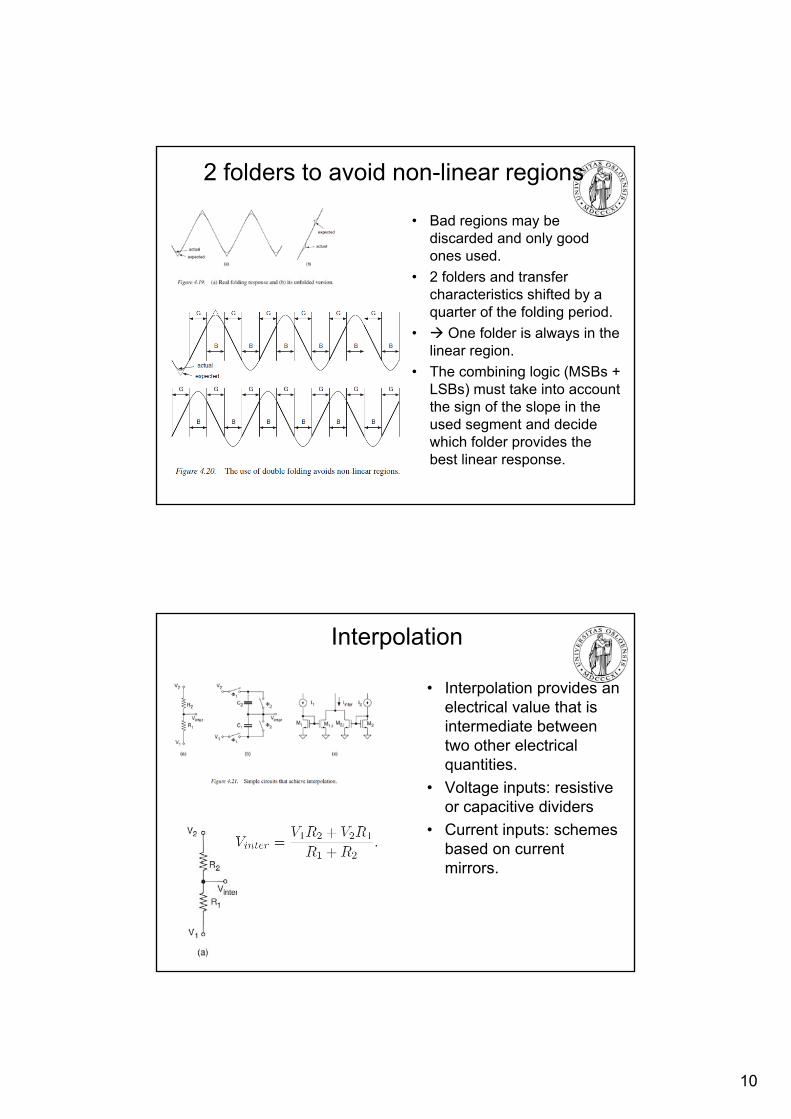
10
2 folders to avoid non-linear regions
• Bad regions may be discarded and only goodones used.
• 2 folders and transfer characteristics shifted by a quarter of the folding period.
• One folder is always in thelinear region.
• The combining logic (MSBs + LSB ) t t k i t tLSBs) must take into accountthe sign of the slope in theused segment and decidewhich folder provides thebest linear response.
Interpolation
• Interpolation provides an electrical value that is intermediate betweentwo other electricalquantities.
• Voltage inputs: resistiveor capacitive dividers
• Current inputs: schemesbased on currentbased on currentmirrors.

11
Interpolation in Flash ADCs (ch. 4.5.4)
• Reduces the number of preamplifiers by generating the median of adjacentpre-amplifier outputs. This interpolated voltage is then used by intermediate latchesintermediate latches.
• Equal slopes at the zero crossing equalize the speed and themetastabilityu error of the latches.
• The number of pre-amps ( and reference voltages diminish by a factor of 2, reducing the capacitive load on the S/H. (may be extended to 4 or 8 resistors between neighbouring pre-amplifiers.
• less power consumption or higher speed.
Time-Interleaved Converters (ch. 4.5.4)
• Converters working in parallel for simultaneous quantization of input samples.
• A suitable combination of the results makes the operation equivalent to a• A suitable combination of the results makes the operation equivalent to a single converter whose speed has been increased by a factor equal to thenumber of parallel elements.
• An alternative solution that relaxes the demanding specification associatedwith one full speed S/H employs one S/H in each path.
• Problems: gain mismatch between channels transformed into dynamicerrors.

12
Time-Interleaved – best compromise between complexity and sampling rate – may be used for
different architectures [Elbjornsson ’05]
Pipeline Converters (ch. 4.8)
• Two-step expanded to aTwo-step expanded to a multi-step algorithm and implemented as a pipeline architecture.
• May generate multiple bits / stage.
• Total resolution is given by• Total resolution is given by the sum of the bits at eachstage.
• Fig. 4.36: generic pipeline stage.

13
Pipelined ADC -example
Integrating converters (ch. 4.9.2)
• Input signal determinesInput signal determinesthe slope of the output from the integrator.
• When it’s shifted, theslope becomes fixed, and the time it takes to return is measured by areturn is measured by a counter, and translatedto a digital output.

14
Integrating Converters (13.1)
ControlCounter
b1b2b3
S2
S1Vin–
Vref
S1S2
R1
C1
Vx
Comparator
• Vx(t) = Vin t / RC (Vx ramp derivative depending on Vin )• High linearity and low offset/gain error
(Vin is held constant during conversion.)
logicCounter 3
bN
Clock
fclk1
Tclk-----------=
Bout
g y g• Small amount of circuitry• Low conversion speed
– 2N+1 * 1/Tclk (Worst case)
Integrating ConvertersVx
Phase (I) Phase (II)
V
Vin3–
(Constant slope)
TimeT1
Vin1–
Vin2–
• The digital output is given by the count at the end of T2
• The digital output value is independent of the time-constant RC
T2(Three values for three inputs)

15

16
Metastability – probability of undefined comparator output (ch. 4.2.1)
• A sampled-data comparatoris typically realized using a pre-amplifier and a latchpre amplifier and a latch.
• Φamp , Φlatch (latch logic level)
• If Vin,d is too small, thecomparator may be undefined at the end of thelatch phase giving an error in the output code and possiblythe output code and possiblycausing a code bubble errorin the thermometric output ofsome converter architectures(or other circuits making useof comparators).
Metastability – probability of undefined comparator output (ch. 4.2.1)
• V0 : voltage swing for valid logic levels
• t = Φ Probability of a• tr = Φlatch Probability of a metastability error increaseswith the sampling frequencyand at high frequenciesbecomes equal to 1 (sincemore than 1 is not a valid result If PE is according toresult. If PE is according to eq. 4.11 > 1, the resultmeans PE is 1.)
• PE is inversely proportional to the input amplitude Vin,d .
The exponential function y = ex

17
Approximate Evaluation of max frequency of operation for ADCs (1/2)
• fTech: Technology unity gainfrequency
• fT: unity gain frequency of OTA or op-ampop-amp
• fT = fTech / α , where α is at least 2-4 (ultimately depending on accuracy).
• fCK = fT / γ , where γ is a suitablemargin between the op-amps fT and the clock frequency, fCK, as sometime for settling is needed. (fCK < fT )
• In order to estimate γ, suppose thatth i t V i t t t 0
• AOL = Vout/(V+ - V-)
the input Vin is a step at t = 0.
• A single pole band-limitation givesrise to an output Vout (t) (approachingVin) given by:
33The exponential function y = ex
Approximate Evaluation of max frequency of operation for ADCs (2/2)
• fTech: Technology unity gain frequency
• fT: unity gain frequency of OTA or op-amp
• fT = fTech / α , where α is at least 2-4 (ultimately depending on accuracy).
• Since an n-bit ADC needs an accuracybetter than 2-(n+1), the settling time must be
( y p g y)
• fCK = fT / γ , where γ is a suitable margin between the op-amps fT and the clockfrequency, fCK, as some time for settling is needed. (fCK < fT )
• In order to estimate γ, suppose that theinput Vin is a step at t = 0.
• A single pole band-limitation gives rise to an output Vout (t) (approaching Vin) given by:
• Since the time allowed for settling is half clock frequencyby:
• Th
34
clock frequency.
β - feedback factor - how much of the output is fed back to the negative input

18
Litterature
• Johns & Martin: ”Analog Integrated Circuit Design”
• Franco Maloberti: ”Data Converters”
• http://inst.eecs.berkeley.edu/~ee247/fa04/fa04/lectures/L19_f04.pdf
35
Next week, 01/03:
• Next week: To be defined..
• Messages are given on the INF4420 homepage.
• Questions: [email protected] , 22852703 / 90013264