nand flash qualification guidelines - nasa · nand flash qualification guideline jason heidecker...
TRANSCRIPT

NAND Flash Qualification Guideline
Jason Heidecker Jet Propulsion Laboratory, California Institute of Technology
National Aeronautics and Space Administration
NEPP Electronic Technology Workshop June 11-13, 2012
1 To be presented at the 3rd NASA Electronic Parts and Packaging (NEPP) Program Electronic Technology Workshop June 11-13, 2012, NASA GSFC, Greenbelt, MD.
© 2012 California Institute of Technology. Government sponsorship acknowledged.

To be presented at the 3rd NASA Electronic Parts and Packaging (NEPP) Program Electronic Technology Workshop June 11-13, 2012, NASA GSFC, Greenbelt, MD. 2
Table of Contents
1. NAND Overview 2. Floating Gate Memory 3. Array Organization 4. Operation 5. Applications 6. Reliability Issues 7. Failure Modes 8. Screening & Qualification 9. System Level Considerations 10. Other Recommendations 11. End of the Road for Flash? 12. Sources/References

To be presented at the 3rd NASA Electronic Parts and Packaging (NEPP) Program Electronic Technology Workshop June 11-13, 2012, NASA GSFC, Greenbelt, MD.
What is NAND Flash?
3
• Unique architecture.
• PROGRAM/READ by PAGE.
• ERASE by BLOCK.
• Built on CMOS. TSOP packages.
• Nonvolatile; low standby power.
• VERY high density.
• Mature technology, billions of chips produced over decades.
Only memory to offer both Gb density and nonvolatility.

To be presented at the 3rd NASA Electronic Parts and Packaging (NEPP) Program Electronic Technology Workshop June 11-13, 2012, NASA GSFC, Greenbelt, MD.
Floating Gate Memory Cell
4
Ref [1]
To be presented at the 3rd NASA Electronic Parts and Packaging (NEPP) Program Electronic Technology Workshop June 11-13, 2012, NASA GSFC, Greenbelt, MD.
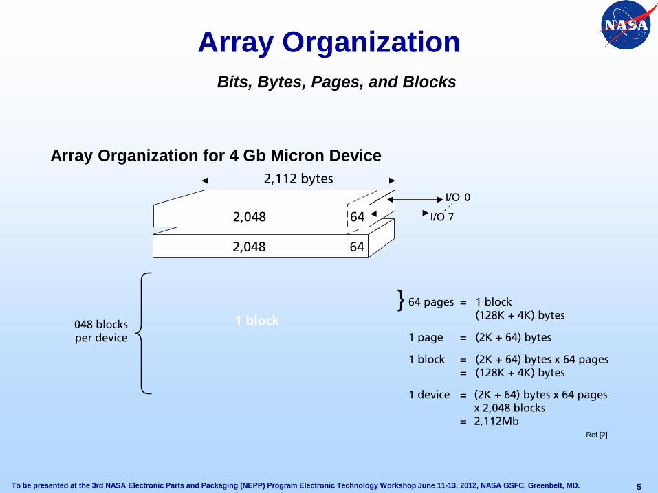
Array Organization
5
Array Organization for 4 Gb Micron Device
Bits, Bytes, Pages, and Blocks
Ref [2]

To be presented at the 3rd NASA Electronic Parts and Packaging (NEPP) Program Electronic Technology Workshop June 11-13, 2012, NASA GSFC, Greenbelt, MD.
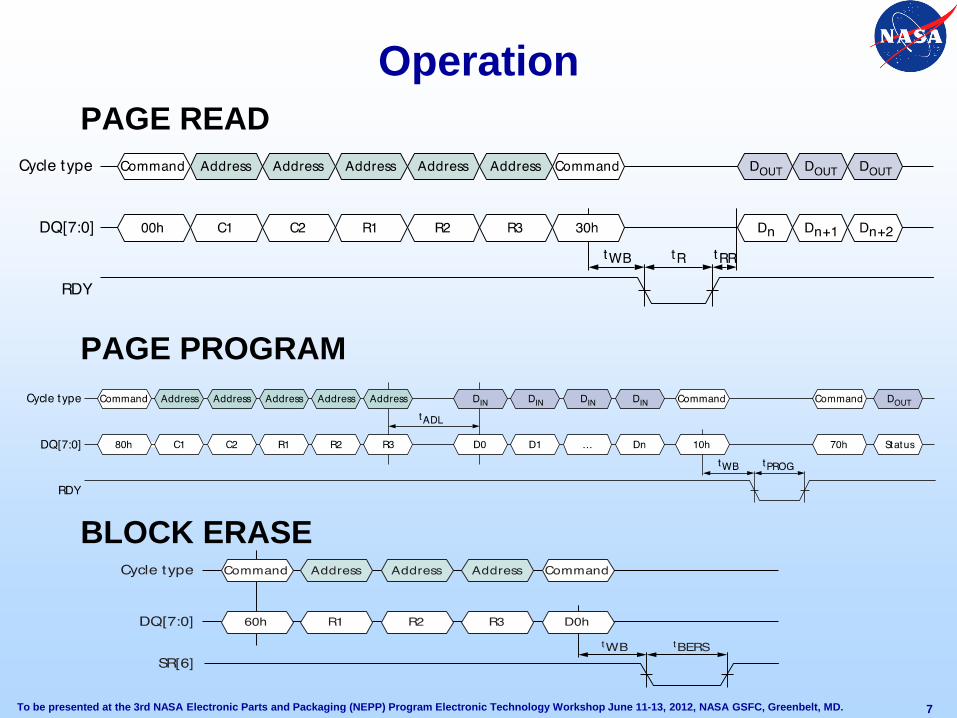
Operation Commands, Addresses, and Data On Same I/O
6 Ref [2]
To be presented at the 3rd NASA Electronic Parts and Packaging (NEPP) Program Electronic Technology Workshop June 11-13, 2012, NASA GSFC, Greenbelt, MD.
Operation PAGE READ PAGE PROGRAM BLOCK ERASE
7

To be presented at the 3rd NASA Electronic Parts and Packaging (NEPP) Program Electronic Technology Workshop June 11-13, 2012, NASA GSFC, Greenbelt, MD.
Applications
8
COMMERCIAL • Mobile Computing
– Cell Phones – MP3 – “Thumb” Drives
• Hard Drives – “Instant On” discs
SPACE • NVM Data Storage
– Engineering & Science Data
10 x 128 Gb MLC NAND Flash parts on space project (JPL)
Ref [3]

To be presented at the 3rd NASA Electronic Parts and Packaging (NEPP) Program Electronic Technology Workshop June 11-13, 2012, NASA GSFC, Greenbelt, MD.
NVM Market
9
Ref [4]

To be presented at the 3rd NASA Electronic Parts and Packaging (NEPP) Program Electronic Technology Workshop June 11-13, 2012, NASA GSFC, Greenbelt, MD.
Reliability Issues
10
• Reliability (bit errors) is getting worse with newer NAND technologies.
• Smaller Vth/level = More Errors
• Fowler-Nordheim Tunneling for Erase and Program uses destructive high voltages ~20 V
NAND Reliability
Smaller Margins Means Less Reliability (Susceptibility to disturb and Stress Induced
Leakage Current (SILC))
Four Areas of Focus: 1. Bad Blocks 2. Endurance 3. Retention 4. Disturb
Ref [5]

To be presented at the 3rd NASA Electronic Parts and Packaging (NEPP) Program Electronic Technology Workshop June 11-13, 2012, NASA GSFC, Greenbelt, MD.
Bad Blocks
11
• Devices are expected to ship with a specified number of bad blocks.
• Specification can be as high as 5%. – Parts may be shipped with 1% bad blocks, but spec says device should not
exceed 5% bad blocks (in this case) before endurance specification is met.
• Blocks will “go bad” with use.
• Bad block is defined as having a certain bit error rate (BER).
For example, a particular 64 Gb Micron TLC device has 2736 blocks: • Spec says: it has an
– endurance specification of 500 cycles – minimum number of valid block of 2626 – 60-bit ECC required per 1146 bytes of data
Therefore, the user should never see more than 60 bit errors per 1146 bytes of data in more than 110 blocks, up to 500 cycles.

To be presented at the 3rd NASA Electronic Parts and Packaging (NEPP) Program Electronic Technology Workshop June 11-13, 2012, NASA GSFC, Greenbelt, MD.
Data Retention
12
Ref [6]

To be presented at the 3rd NASA Electronic Parts and Packaging (NEPP) Program Electronic Technology Workshop June 11-13, 2012, NASA GSFC, Greenbelt, MD.
Endurance
13
Ref [7]

To be presented at the 3rd NASA Electronic Parts and Packaging (NEPP) Program Electronic Technology Workshop June 11-13, 2012, NASA GSFC, Greenbelt, MD.
Read Disturb
14
• Flash also susceptible to Program and Erase Disturb, but only Read disturb is prevalent in modern devices
• Read Disturb confined to block being operated on
• Stressed cells are in unselected pages
• Nondestructive
• Disturb occurs when charge collects on the floating gate, causing the cell to appear weakly programmed
Ref [8]
To be presented at the 3rd NASA Electronic Parts and Packaging (NEPP) Program Electronic Technology Workshop June 11-13, 2012, NASA GSFC, Greenbelt, MD.
Failure Modes
15
To be presented at the 3rd NASA Electronic Parts and Packaging (NEPP) Program Electronic Technology Workshop June 11-13, 2012, NASA GSFC, Greenbelt, MD.
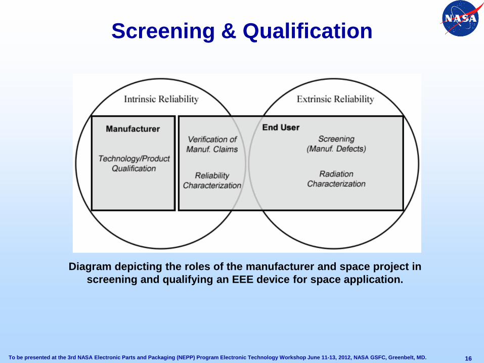
Screening & Qualification
16
Diagram depicting the roles of the manufacturer and space project in screening and qualifying an EEE device for space application.

To be presented at the 3rd NASA Electronic Parts and Packaging (NEPP) Program Electronic Technology Workshop June 11-13, 2012, NASA GSFC, Greenbelt, MD.
Screening
17

To be presented at the 3rd NASA Electronic Parts and Packaging (NEPP) Program Electronic Technology Workshop June 11-13, 2012, NASA GSFC, Greenbelt, MD.
Qualification
18

To be presented at the 3rd NASA Electronic Parts and Packaging (NEPP) Program Electronic Technology Workshop June 11-13, 2012, NASA GSFC, Greenbelt, MD.
Reliability Characterization
19

To be presented at the 3rd NASA Electronic Parts and Packaging (NEPP) Program Electronic Technology Workshop June 11-13, 2012, NASA GSFC, Greenbelt, MD.
Endurance Cycling
20
64 Gb TLC
32 Gb MLC
8 Gb SLC
Bit Error Rate (BER) Vs. E/P/R Cycles Micron NAND Flash
E/P/R Cycles
Bit
Erro
r Rat
e (B
ER)
Data from Heidecker (JPL). NEPP 2010, 2011, 2012.
Ref [9]
To be presented at the 3rd NASA Electronic Parts and Packaging (NEPP) Program Electronic Technology Workshop June 11-13, 2012, NASA GSFC, Greenbelt, MD.
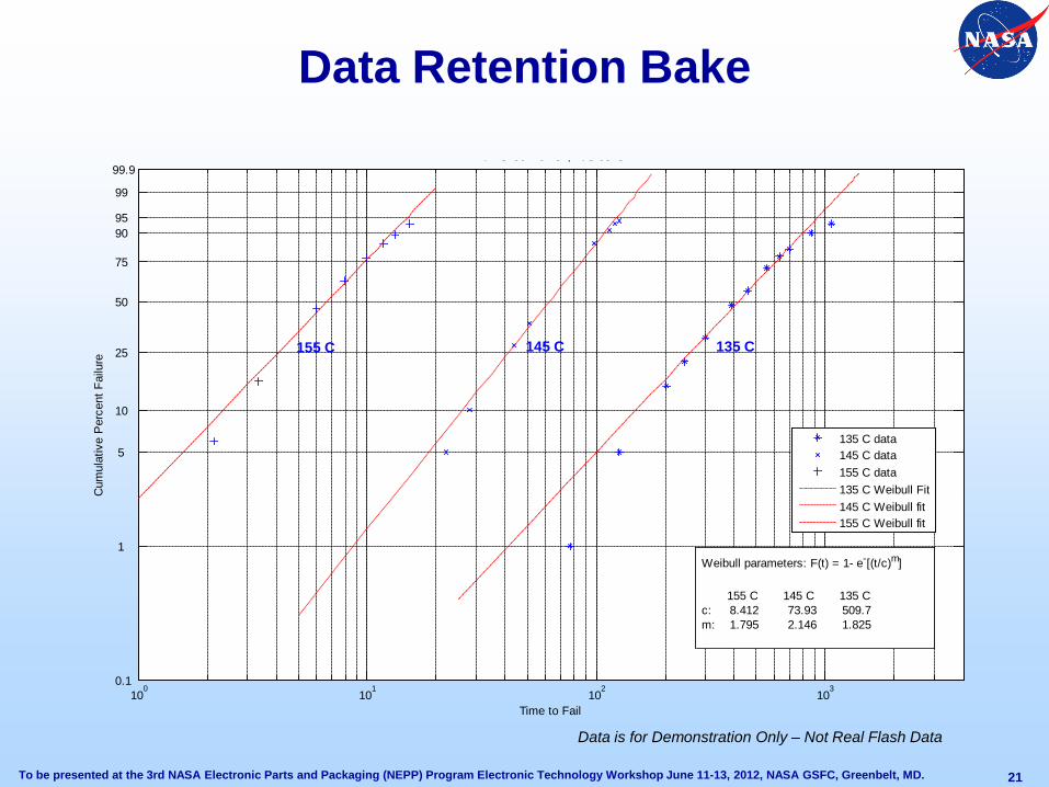
Data Retention Bake
21
100
101
102
103
0.1
1
5
10
25
50
75
90 95
99
99.9
/ 8 06 6 5 , /C 08 8
Time to Fail
Cum
ulat
ive
Per
cent
Fai
lure
135 C data145 C data155 C data135 C Weibull Fit145 C Weibull fit155 C Weibull fit
155 C 145 C 135 C
Weibull parameters: F(t) = 1- e-[(t/c)m]
155 C 145 C 135 Cc: 8.412 73.93 509.7m: 1.795 2.146 1.825
Data is for Demonstration Only – Not Real Flash Data

To be presented at the 3rd NASA Electronic Parts and Packaging (NEPP) Program Electronic Technology Workshop June 11-13, 2012, NASA GSFC, Greenbelt, MD.
Read Disturb
22
• PURPOSE – Measure how BER worsens with multiple reads of block of data
• DISTURB TEST 1. Erase 2. Program 3. Read many times
• Repeat test after cycling device. Perform at:
– 0x – 0.5x – 1.0x – 1.5x
Bit Errors Vs Number of Reads
Read disturb error rate much worse in parts that have consumed erase/program/read cycles.
Cycled 1.0x spec
Uncycled
Ref [10]
To be presented at the 3rd NASA Electronic Parts and Packaging (NEPP) Program Electronic Technology Workshop June 11-13, 2012, NASA GSFC, Greenbelt, MD.
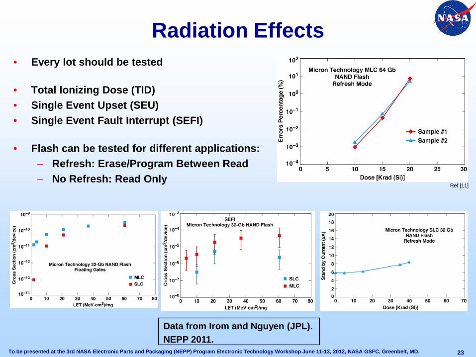
Radiation Effects
23
• Every lot should be tested
• Total Ionizing Dose (TID) • Single Event Upset (SEU) • Single Event Fault Interrupt (SEFI)
• Flash can be tested for different applications:
– Refresh: Erase/Program Between Read – No Refresh: Read Only
Data from Irom and Nguyen (JPL). NEPP 2011.
Ref [11]

To be presented at the 3rd NASA Electronic Parts and Packaging (NEPP) Program Electronic Technology Workshop June 11-13, 2012, NASA GSFC, Greenbelt, MD.
Worst Case UBER Calculation
24
When calculating uncorrectable bit error rate (UBER) from raw NAND bit error rate (BER), the worst case BER should be used. Here’s a general example, but users should tailor to their specific application or use case:
BERworst case = BERradiation + BERcycling + BERdisturb
10-5
10-7

To be presented at the 3rd NASA Electronic Parts and Packaging (NEPP) Program Electronic Technology Workshop June 11-13, 2012, NASA GSFC, Greenbelt, MD.
System Level Considerations
25
Error Correction Codes (ECC) – Always required with NAND Flash.
NAND Type
Datasheet ECC Requirement Corresponding Bit Error Rate
Recommended ECC
SLC 1-bit ECC per 528 bytes of data 0.02% SEC/DEC Hamming Code or Reed-Solomon Code
MLC 12-bit ECC per 539 bytes of data 0.28% BCH Algorithms
TLC 60-bit ECC per 1146 bytes of data 0.65% Low Density Parity Check (LDPC) Codes

To be presented at the 3rd NASA Electronic Parts and Packaging (NEPP) Program Electronic Technology Workshop June 11-13, 2012, NASA GSFC, Greenbelt, MD.
Other Recommendations
26
• Pure Tin Leads – All NAND Flash are PEMS, which have pure tins
leads. Leads must be retinned or solder-dipped before installation onto flight boards.
• Disturb Error Mitigation – Limit the number of reads between programming,
sequentially program pages in a block, and minimize partial-page programming [Ref: 12].
• Moisture Sensitivity (PEMS Storage) – Plastic packaging is hygroscopic – Need to be stored in humidity controlled environments – Should be “baked out” prior to assembly to prevent popcorning or other damage
• Electrostatic Discharge (ESD) Sensitivity – Most NAND Flash devices are classified has having ESD sensitivities of Class 1C
(>1000 V HBM) or better. – Most standard ESD practices (static dissipative wrist straps, workbenches, and
storage bags) will prevent damaging the device.
To be presented at the 3rd NASA Electronic Parts and Packaging (NEPP) Program Electronic Technology Workshop June 11-13, 2012, NASA GSFC, Greenbelt, MD.
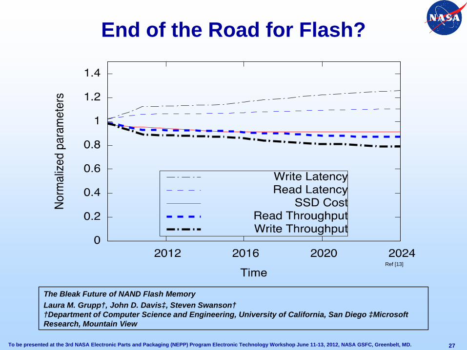
End of the Road for Flash?
27
The Bleak Future of NAND Flash Memory Laura M. Grupp†, John D. Davis‡, Steven Swanson† †Department of Computer Science and Engineering, University of California, San Diego ‡Microsoft Research, Mountain View
Ref [13]
To be presented at the 3rd NASA Electronic Parts and Packaging (NEPP) Program Electronic Technology Workshop June 11-13, 2012, NASA GSFC, Greenbelt, MD.
What’s Next?
Could it be MRAM?
Stay Tuned…
28

To be presented at the 3rd NASA Electronic Parts and Packaging (NEPP) Program Electronic Technology Workshop June 11-13, 2012, NASA GSFC, Greenbelt, MD.
Sources/References 1. Bez, R. “Introduction to Flash Memory.” Proceedings of the IEEE, Vol. 91, No. 4, April 2003.
2. 4 Gb NAND SLC Datasheet, “2_4_8gb_nand_m49a__1.fm - Rev. D 12/06 EN.” Micron, Inc.
3. TN-29-19, “NAND Flash 101: An Introduction to NAND Flash and How to Design It In to Your Next Product.”
Micron, Inc.
4. Jung, T.S. “Memory Technology and Solutions Roadmap,” Samsung Analyst Day, 2005.
5. Yaakobi, L. “Characterization and Error-Correcting Codes for TLC Flash Memories.” International Conference on Computing, Networking and Communications, Data Storage Technology and Applications Symposium, 2012.
6. Lee, J. “Degradation of Tunnel Oxide by FN Current Stress and Its Effects On Data Retention Characteristics of 90-nm NAND Flash Memory Cells,” IRPS, 2003.
7. Desnoyers, P. “Empirical Evaluation of NAND Flash Memory Performance,” HotStorage, 2009.
8. Prouty, W. “NAND Flash Reliability and Performance, The Software Effect.” Flash Memory Summit, 2007.
9. Heidecker, J. “NAND Flash Screening and Qualification Guideline for Space Application.” NASA Electronics and Packaging Program (NEPP), 2011.
10. Qualification data for 128 Gb MCM MLC NAND for SMAP Mission, JPL, 2010.
11. Irom, F. “Radiation Tests of Highly Scaled, High-Density, Commercial, Nonvolatile NAND Flash Memories,” NASA Electronic Parts and Packaging Program (NEPP), 2011.
12. Sheldon, D. “Disturb Testing in Flash Memories.” NASA Electronic Parts and Packaging Program (NEPP), 2009.
13. Grupp, L. “The Bleak Future of NAND Flash Memory.” University of San Diego, 2011.
29