nandha engineering college
TRANSCRIPT
Approved by third Academic council
NANDHA ENGINEERING COLLEGE
(An Autonomous Institution affiliated to Anna University Chennai and approved by AICTE, New Delhi)
Erode-638 052, Tamilnadu, India, Phone: 04294 – 225585
Curriculum and Syllabus for
M.E – VLSI Design [R15]
(This Curriculum and Syllabi are applicable to Students admitted from the academic year 2015-2016 onwards)
JUNE 2015

Approved by third Academic council
NANDHA ENGINEERING COLLEGE, ERODE-52
REGULATIONS 2015
I SEMESTER CURRICULUM
M.E. (VLSI DESIGN)
SEMESTER I
THEORY
Course code Course Title L T P C
15AE101 Applied Mathematics for Electronics Engineers 3 1 0 4
15VL101 DSP Integrated Circuits 3 0 0 3
15AE103 Digital System for IC Design 3 0 0 3
15VL102 VLSI Design Techniques 3 0 0 3
15VL103 Device Modeling and Simulation 3 0 0 3
E1 Elective I ( PE) 3 0 0 3
PRACTICAL
Course code Course Title L T P C
15VL111 VLSI Design Lab I 0 0 4 2
15VL121 Technical Seminar-I 0 0 2 1
TOTAL 18 1 6 22
SEMESTER II
THEORY
Course code Course Title L T P C
15AE201 Analysis and Design of Analog Integrated Circuits 3 0 0 3
15VL201 CAD for VLSI Circuits 3 0 0 3
15AE202 Computer Architecture and Parallel Processing 3 0 0 3
15AE204 Advanced Embedded Systems 3 0 0 3
E2 Elective II ( PE) 3 0 0 3
E3 Elective III ( PE) 3 0 0 3
PRACTICAL
Course code Course Title L T P C
15VL211 VLSI Design Lab II 0 0 4 2
15VL221 Technical Seminar-II 0 0 2 1
TOTAL 18 0 4 21

Approved by third Academic council
SEMESTER III
THEORY
Course code Course Title L T P C
E4 Elective IV ( PE) 3 0 0 3
E5 Elective V ( PE) 3 0 0 3
E6 Elective VI ( OE) 3 0 0 3
PRACTICAL
Course code Course Title L T P C
15VL331 Project Work (Phase I) 0 0 12 6
TOTAL
9
0
12
15
SEMESTER IV
PRACTICAL
Course code Course Title L T P C
15VL431 Project Work (Phase II) 0 0 24 12
TOTAL
0
0
24
12

Approved by third Academic council
NANDHA ENGINEERING COLLEGE, ERODE-52
REGULATIONS 2015
M.E. (VLSI DESIGN)
I TO VI SEMESTERS (PART TIME) CURRICULUM AND SYLLABUS
SEMESTER I
THEORY
Course code Course Title L T P C
15AE101 Applied Mathematics for Electronics Engineers 3 1 0 4
15AE103 Digital System for IC Design 3 0 0 3
15VL102 VLSI Design Techniques 3 0 0 3
PRACTICAL
Course code Course Title L T P C
15VL111 VLSI Design Lab I 0 0 4 2
15VL121 Technical Seminar-I 0 0 2 1
TOTAL 9 1 6 13
SEMESTER II
THEORY
Course code Course Title L T P C
15AE201 Analysis and Design of Analog Integrated Circuits 3 0 0 3
15VL201 CAD for VLSI Circuits 3 0 0 3
15AE204 Advanced Embedded Systems 3 0 0 3
PRACTICAL
Course code Course Title L T P C
15VL211 VLSI Design Lab II 0 0 4 2
15VL221 Technical Seminar-II 0 0 2 1
TOTAL 9 0 6 12

Approved by third Academic council
SEMESTER III
THEORY
Course code Course Title L T P C
15VL101 DSP Integrated Circuits 3 0 0 3
15VL103 Device Modeling and Simulation 3 0 0 3
E1 Elective I ( PE) 3 0 0 3
TOTAL 9 0 0 9
SEMESTER IV
THEORY
Course code Course Title L T P C
15AE202 Computer Architecture and Parallel Processing 3 0 0 3
E2 Elective II ( PE) 3 0 0 3
E3 Elective III ( PE) 3 0 0 3
TOTAL 9 0 0 9
SEMESTER V
THEORY
Course code Course Title L T P C
E4 Elective IV ( PE) 3 0 0 3
E5 Elective V ( PE) 3 0 0 3
E6 Elective VI (OE) 3 0 0 3
PRACTICAL
Course code Course Title L T P C
15VL331 Project Work(Phase I) 0 0 12 6
TOTAL 9 0 12 6
SEMESTER VI
PRACTICAL
Course code Course Title L T P C
15VL431 Project Work (Phase II) 0 0 24 12
TOTAL 0 0 24 12

Approved by third Academic council
LIST OF ELECTIVES
M.E VLSI DESIGN
Professional Electives
ELECTIVES
Course code Course Title L T P C
15AE104 Advanced Microprocessors and Microcontrollers 3 0 0 3
15AEX07 Analog VLSI Design 3 0 0 3
15VLX03 Low Power VLSI Design 3 0 0 3
15VLX04 Physical Design of VLSI Circuits 3 0 0 3
15VLX05 VLSI Technology 3 0 0 3
15VLX06 ASIC Design 3 0 0 3
15VLX07 Testing of VLSI Circuits 3 0 0 3
15VLX01 VLSI for Wireless Communication 3 0 0 3
15VLX02 VLSI Signal Processing 3 0 0 3
15VLX08 System on Chip Design 3 0 0 3
15VLX10 Design of Semiconductor Memories 3 0 0 3
15AEX04 Genetic Algorithm and Applications 3 0 0 3
15VLX09 Security Solutions in VLSI 3 0 0 3
15AEX06 Hardware Software Co-Design 3 0 0 3
Open Electives
ELECTIVES
Course code Course Title L T P C
15AEZ01 Robotics 3 0 0 3
15AEZ02 RF system Design 3 0 0 3
15AEZ03 Electromagnetic Interference and Compatibility in System Design 3 0 0 3
15AEZ04 Reconfigurable Computing 3 0 0 3
TOTAL CREDITS (22+21+15+12) = 70 CREDITS
*PE-Professional Electives *OE-Open Electives

Approved by third Academic council
15AE101 APPLIED MATHEMATICS FOR ELECTRONICS ENGINEERS
L T P C 3 1 0 4
OBJECTIVE:
The course aims at imparting the knowledge of propositions, decompositions and optimality. The course aims at providing necessary mathematical support and confidence to tackle real life problems.
COURSE OUTCOMES:
On completion of this course the student will be able to CO 1.To develop efficient algorithms for solving dynamic programming problems, to acquire skills in handling situation involving random variable. CO 2.To learn the basics and gained the skill for specialized studies and research.
CO 3.To exposed the basic characteristic features of a queuing system and acquire skills in analyzing queuing models. CO 4.To understands the basic principles of fuzzy logic.
UNIT I FUZZY LOGIC (9+3) Classical logic – Multivalued logics – Fuzzy propositions – Fuzzy quantifiers.
UNIT II MATRIX THEORY (9+3)
Some important matrix factorizations – The Cholesky decomposition – QR factorization –Pseudo inverse - Least squares method – Singular value decomposition.
UNIT III ONE DIMENSIONAL RANDOM VARIABLES (9+3) Random variables – Probability function – moments – moment generating functions and their properties – Binomial, Poisson, Geometric, Uniform, Exponential, Gamma and Normal distributions
UNIT IV DYNAMIC PROGRAMMING (9+3) Dynamic programming – Principle of optimality – Forward and backward recursion – Applications of dynamic programming: Cargo loading method – Workforce size model – Equipment replacement model.
UNIT V QUEUING MODELS (9+3) Poisson Process – Markovian queues – Single and Multi-server Models – Little‟s formula – Machine Interference Model – Steady State analysis – Self Service queue.
TOTAL: L: 45 +T:15= 60 PERIODS REFERENCES:
1. George J. Klir and Yuan, B., Fuzzy sets and fuzzy logic, Theory and applications, Prentice Hall of India Pvt. Ltd., 1997.
2. Moon, T.K., Sterling, W.C., Mathematical methods and algorithms for signal processing, Pearson Education, 2000.
3. Richard Johnson, Miller & Freund‟s, Probability and Statistics for Engineers, 7th Edition, Prentice – Hall of India, Private Ltd., New Delhi (2007).
4. Taha, H.A., Operations Research, An introduction, 7th edition, Pearson education editions, Asia, New Delhi, 2002.
5. Donald Gross and Carl M. Harris, Fundamentals of Queuing theory, 2nd edition, John Wiley and Sons, New York (1985).
Approved by third Academic council
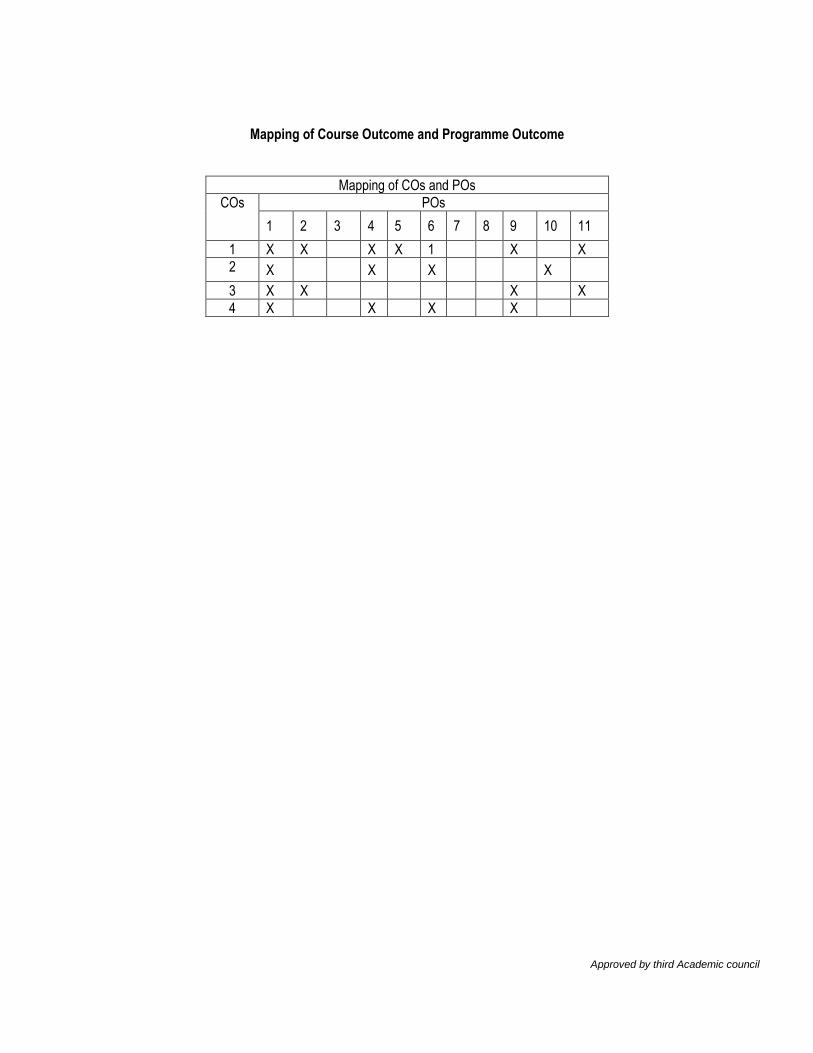
Mapping of Course Outcome and Programme Outcome
Mapping of COs and POs
COs POs
1 2 3 4 5 6 7 8 9 10 11
1 X X X X 1 X X
2 X X X X
3 X X X X
4 X X X X

Approved by third Academic council
15VL101 - DSP INTEGRATED CIRCUITS
L T P C 3 0 0 3
OBJECTIVES:
To familiarize the fundamental concepts of Signal processing.
To gain knowledge about filter design in Digital Signal Processing.
To acquire sound knowledge about TMS processors.
To understand the concepts of Transformations in signal processing.
LEARNING OUTCOMES:
On completion of this course the student will be able to CO 1. Implement various signal processing algorithms. CO 2. Diagnose the design and methodologies in hardware and software design. CO 3. Identify new developments in Application specific processors.
UNIT I DSP INTEGARTED CIRCUITS AND VLSI CIRCUIT TECHNOLOGIES (9) Standard digital signal processors - Application specific IC‟s for DSP - DSP systems - DSP system design – Integrated circuit design - MOS transistors - MOS logic - VLSI process technologies
UNIT II - DIGITAL SIGNAL PROCESSING (9)
Digital signal processing - Sampling of analog signals - Selection of sample frequency - Signal processing systems -Frequency response - Transfer functions - Signal flow graphs - Filter structures- Adaptive DSP algorithms - DFT - FFT- Image coding - Discrete cosine transforms. UNIT III - DIGITAL FILTERS AND FINITE WORD LENGTH EFFECTS (9) FIR filters - FIR filter structures - IIR filters - Specifications of IIR filters - Mapping of analog transfer functions - Mapping of analog filter structures - Multirate systems – Interpolation with an integer factor L - Sampling rate change with a ratio L/M - Multirate filters - Finite word length effects - Parasitic oscillations - Scaling of signal levels – Roundoff noise - Measuring round-off noise - Coefficient sensitivity- Sensitivity and noise.
UNIT IV - DSP ARCHITECTURES AND SYNTHESIS OF DSP ARCHITECTURES (9) DSP system architectures - Ideal DSP architectures – Multiprocessors and multicomputers - Systolic and Wave front arrays - Shared memory architectures - Mapping of DSP algorithms onto hardware - Implementation based on complex PEs - Shared memory architecture with Bit - serial PEs.
UNIT V - NUMBER SYSTEMS - ARITHMETIC UNITS AND INTEGARTED CIRCUIT DESIGN (9) Conventional number system - Redundant Number system - Residue Number System - Bit-parallel and Bit-Serial arithmetic - Basic shift accumulator - Reducing the memory size – Complex multipliers - Layout of VLSI circuits
TOTAL = 45 PERIODS REFERENCES: 1. Lars Wanhammer, “DSP Integrated Circuits”, Academic press, New York, 1999. 2. A.V. Oppenheim et.al, “Discrete-time Signal Processing “, Pearson education, 2000. 3. Keshab K.Parhi, “VLSI digital Signal Processing Systems design and Implementation”, JohnWiley & Sons,1999. 4. Emmanuel C. Ifeachor, Barrie W. Jervis, “Digital signal processing, A practical approach” , 2nd edition, Prentice Hall, 2001.

Approved by third Academic council
Mapping of Course Outcome and Programme Outcome
Mapping of COs and POs
COs POs
1 2 3 4 5 6 7 8 9 10 11
1 x x x x x
2 x x x x x x
3 x x x x x

Approved by third Academic council
15AE103 DIGITAL SYSTEM FOR IC DESIGN
L T P C 3 0 0 3
OBJECTIVES:
To know about analysis and Design of Synchronous and Asynchronous sequential machines
To draw a ASM chart for digital designs
To learn about different faults in digital circuits and methods of detection and diagnosing
To Know about Types of PLD‟s and architecture of FPGA‟s To have knowledge about digital circuit design by VHDL programming.
LEARNING OUTCOMES:
On completion of this course the students will be able to CO 1. Analysis and Design of Synchronous and Asynchronous sequential machines CO 2. Draw a ASM chart for digital designs CO 3. Detect and diagnosis different faults in digital circuits CO 4. Have knowledge of PLD‟s and architecture of FPGA‟s
CO 5.Design the digital systems through VHDL programming.
UNIT I - SEQUENTIAL CIRCUIT DESIGN (9)
Analysis of clocked synchronous sequential circuits and modeling-State diagram, state table, state table assignment and reduction-Design of synchronous sequential circuits- ASM chart and System design using ASM Realization by using Multiplexer & PLA
UNIT II - ASYNCHRONOUS SEQUENTIAL CIRCUIT DESIGN (9)
Analysis of asynchronous sequential circuit –flow table reduction-races-state assignment transition table and problems in transition table-design of asynchronous sequential circuit-Static, dynamic and essential hazards –data synchronizers – mixed operating mode asynchronous circuits –designing vending machine controller
UNIT III- FAULT DIAGNOSIS AND TESTABILITY ALGORITHMS (9)
Fault table method-path sensitization method –Boolean difference method-D algorithm -Tolerance techniques – Fault in PLA –Test generation-DFT schemes–Built in self test
UNIT IV - SYNCHRONOUS DESIGN USING PROGRAMMABLE DEVICES (9)
Programming logic device families–Designing a synchronous sequential circuit using PLA/PAL Altera MAX 7000 –FPGA –Xilinx FPGA-Xilinx 4000,
UNIT V- SYSTEM DESIGN USING VERILOG (9)
Verilog operators –Arrays –concurrent and sequential statements –Data flow – Behavioral –structural modeling –Test bench -Using Subcircuits- Realization of combinational and sequential circuits –Registers –counters – sequential machine –serial adder –Multiplier-Divider
TOTAL: L: 45 = 45 PERIODS REFERENCES: 1. Stephen Brown, Zvonko Vranesic “ Fundamentals of Digital Logic with Verilog Design” 2nd Edition Tata McGraw Hill, 2007 2. Donald D. Givone “Digital Principles and Design” Tata McGraw Hill, 2002 3. Floyd, Floyd Thomas L.” Digital Fundamentals “Pearson Education India, 01-Sep-2005 4. Parag K.Lala “Fault Tolerant and Fault Testable Hardware Design” B S Publications, 2002 5. Parag K.Lala “Digital system Design using PLD” B S Publications, 2003
Approved by third Academic council
Mapping of Course Outcome and Programme Outcome
Mapping of COs and POs
COs POs
1 2 3 4 5 6 7 8 9 10 11
1 x x x x
2 x x x x
3 x x x
4 x x x
5 x x x

Approved by third Academic council
15VL102 VLSI DESIGN TECHNIQUES
L T P C 3 0 0 3
OBJECTIVES:
To understand the concepts of MOS transistors operations and their AC , DC characteristics.
To know the fabrication process of CMOS technology and its layout design rules
To study the concepts of CMOS invertors and their sizing methods
To know the concepts of power estimation and delay calculations in CMOS circuits.
LEARNING OUTCOMES:
On Completion of this course students will be able to CO1. Examine the basic building blocks of large-scale digital integrated circuits
CO 2. Analysis the physical design process of VLSI design flow
CO 3. Implementation of special purpose structures for complex digital systems
UNIT I MOS TRANSISTOR THEORY (9) NMOS and PMOS transistors, CMOS logic, MOS transistor theory –Introduction, Enhancement mode transistor action, Ideal I-V characteristics,DC transfer characteristics, Threshold voltage-Body effect-Design equations-Second order effects. MOS models and small signal AC characteristics, Simple MOS capacitance Models, Detailed MOS gate capacitance model, Detailed MOS Diffusion capacitance model.
UNIT II - CMOS TECHNOLOGY AND DESIGN RULE (9)
CMOS fabrication and Layout, CMOS technologies, P -Well process, N -Well process, twin -tub process, MOS layers stick diagrams and Layout diagram, Layout design rules, Latch up in CMOS circuits, CMOS process enhancements, Technology –related CAD issues, Fabrication and packaging..
UNIT III - INVERTERS AND LOGIC GATES (9) NMOS and CMOS Inverters, Inverter ratio, DC and transient characteristics , switching times, Super buffers, Driving large capacitance loads, CMOS logic structures , Transmission gates, Static CMOS design, dynamic CMOS design.
UNIT IV - CIRCUIT CHARACTERISATION AND PERFORMANCE ESTIMATION (9) Resistance estimation, Capacitance estimation, Inductance, switching characteristics, transistor sizing, power dissipation and design margining. Charge sharing, Scaling.
UNIT V - VLSI SYSTEM COMPONENTS CIRCUITS AND SYSTEM LEVEL PHYSICAL DESIGN (9) Multiplexers, Decoders, comparators, priority encoders, Shift registers. Arithmetic circuits–Ripple carry adders, Carry look ahead adders, High-speed adders, Multipliers. Physical design –Delay modeling, cross talk, floor planning, power distribution. Clock distribution. Basics of CMOS testing.
TOTAL = 45 PERIODS

Approved by third Academic council
REFERENCES: 1.Neil H.E. Weste and Kamran Eshraghian, Principles of CMOS VLSI Design, Pearson Education ASIA, 2ndedition, 2000. 2.John P.Uyemura “Introduction to VLSI Circuits and Systems”, John Wiley & Sons, Inc., 2002. 3.Eugene D.Fabricius, Introduction to VLSI Design McGraw Hill International Editions, 1990. 4.Pucknell, “Basic VLSI Design”, Prentice Hall of India Publication, 1995. 5.Wayne Wolf “Modern VLSI Design System on chip. Pearson Education, 2002.
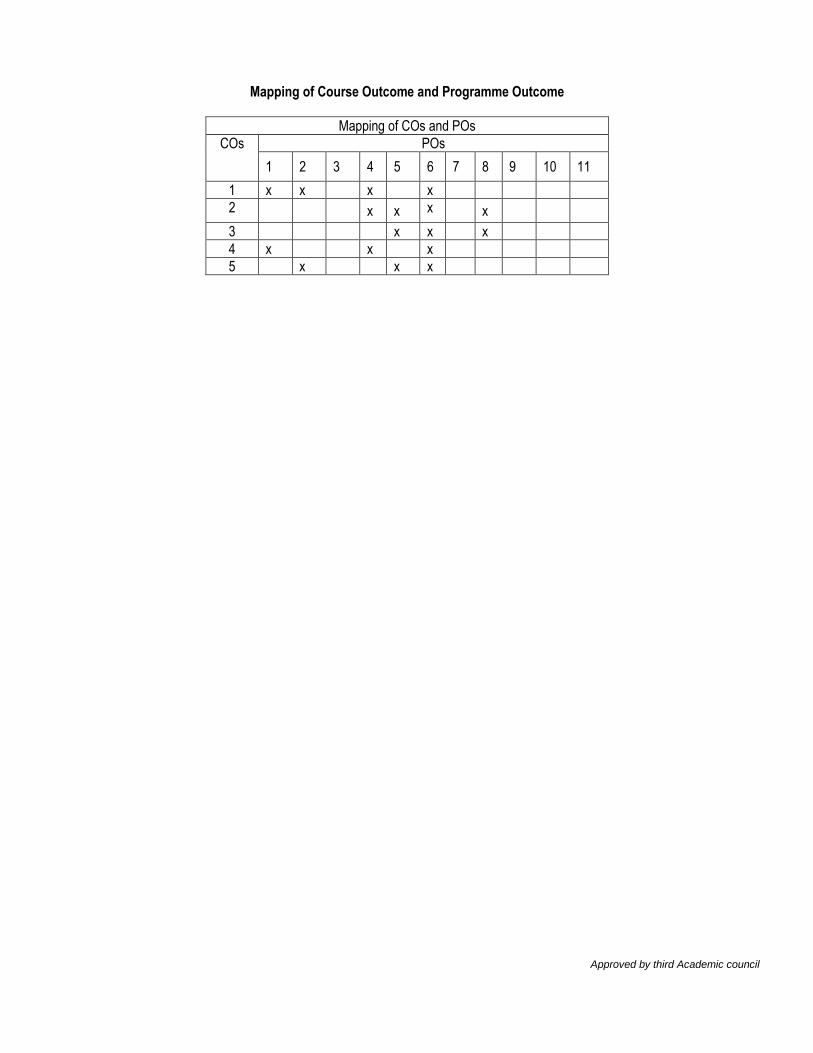
Mapping of Course Outcome and Programme Outcome
Mapping of COs and POs
COs POs
1 2 3 4 5 6 7 8 9 10 11
1 × × ×
2 × × ×
3 × × × × × ×

Approved by third Academic council
15VL103 DEVICE MODELING AND SIMULATION L T P C 3 0 0 3
OBJECTIVES:
To Learn the basics of MOS physics and modeling of MOS structures, MOSFETS, resistance, capacitance and inductance.
To acquire sound knowledge in noise modeling and accurate distortion analysis in analog circuits.
To understand the concept of BSIM modeling and other MOSFET models
To study the concept of non-quasi-static modeling and noise model temperature effects.
LEARNING OUTCOMES: On completion of this course the student will be able to
CO 1. Know about the basics of MOSFET device modeling and noise modeling. CO 2. Understand and apply the concepts of noise modeling in system design CO 3. Apply the mathematical techniques for device simulations
CO 4. Realize concepts about process variation and quality assurance.
UNIT I MOSFET DEVICE PHYSICS (9) MOSFET capacitor, Basic operation, Basic modeling, Advanced MOSFET modeling, RF modeling of MOS transistors, Equivalent circuit representation of MOS transistor, High frequency behavior of MOS transistor and A.C small signal modeling, model parameter extraction, modeling parasitic BJT, Resistors, Capacitors, Inductors.
UNIT II - NOISE MODELS AND BSIM4 MOSFET MODEL (9)
Noise sources in MOSFET-flicker noise modeling thermal noise modeling- BSIM4 MOSFET model-gate dielectric model-enhanced models for Effective dc and ac channel length and width-threshold voltage model-i-v model. UNIT III - OTHER MOSFET MODELS
(9) The EKV model, model features, long channel drain current model, modeling second order effects of the drain current, modeling of charge storage effects, Non- quasi-static modeling, noise temperature effects, MOS model 9, MOSAI model. UNIT IV - MATHEMATICAL TECHNIQUES FOR DEVICE SIMULATIONS
(9) Poisson equation, continuity equation, drift-diffusion equation, Schrodinger equation, hydrodynamic equations, trap rate, finite difference solutions to these equations in 1D and 2D space, grid generation. UNIT V - MODELLING OF PROCESS VARIATION AND QUALITY ASSURANCE
(9) Influence of process variation, modeling of device mismatch for Analog/RF Applications ,Benchmark circuits for quality assurance, Automation of the tests
TOTAL= 45 PERIODS

Approved by third Academic council
REFERENCES:
1. Trond Ytterdal, Yuhua Cheng and Tor A. FjeldlyWayne Wol f, ―Device Modeling for Analog and RF CMOS Circuit Design‖, John Wiley & Sons Ltd.
2. Philip E. Allen, Douglas R.Hoberg, ―CMOS Analog Circuit Design‖, Second Edition, Oxford Press-2002. 3. Kiat Seng Yeo, Samir S. Rofail, Wang-Ling Gob, ―CMOS / BiCMOS CLSI Low Voltage Power‖, Person
education low price edition2002 S.M.Sze, ―Semiconductor Devices –Physics and Technology‖, John Wiley and sons 1985.
4. Grasser, T., “Advanced Device Modeling and Simulation”, World Scientific Publishing Company., 2003 5. Arora, N., “MOSFET Models for VLSI Circuit Simulation”, Springer-Verlag, 1993
Mapping of Course Outcome and Programme Outcome
Mapping of COs and POs
COs POs
1 2 3 4 5 6 7 8 9 10 11
1 x x x x x x
2 x x x x x x
3 x x x
4 x x x x x

Approved by third Academic council
15 VL111 VLSI DESIGN LAB I
L T P C 0 0 4 2
OBJECTIVES:
To learn about digital system designs using HDL codes
To have knowledge of SPICE modelling of Logic gates
To learn about hardware implementation of digital signal processing circuits
To know about microcontroller based designs
LEARNING OUTCOMES:
On completion of this course the students will be able to CO1. Have knowledge about sequential & combinational digital system designs CO2.Perform Transient ,DC analysis and Power analysis of transistor level designs CO3.Have knowledge of hardware implementation of digital signal processing circuits CO4.Design a microcontroller based systems
1. Modelling of Sequential Digital system using VHDL.
2. Modelling of Sequential Digital system using Verilog.
3. Design and Implementation of ALU and MAC unit using FPGA.
4. Simulation of NMOS and CMOS circuits using SPICE.
5. Modelling of CMOS and NMOS Inverter and Logic gates using Tanner.
6. Modelling and analysis of MOS capacitor
7. Design of FIR filters using FPGA
8. Implementation of Stepper Motor control using 89C51 microcontroller.
9. Implementation of Traffic light control using 89C51 microcontroller.
TOTAL = 60 PERIODS
Mapping of Course Outcome and Programme Outcome
Mapping of COs and POs
COs POs
1 2 3 4 5 6 7 8 9 10 11
1 x x x x
2 x x x x x
3 x x x x
4 x x x x

Approved by third Academic council
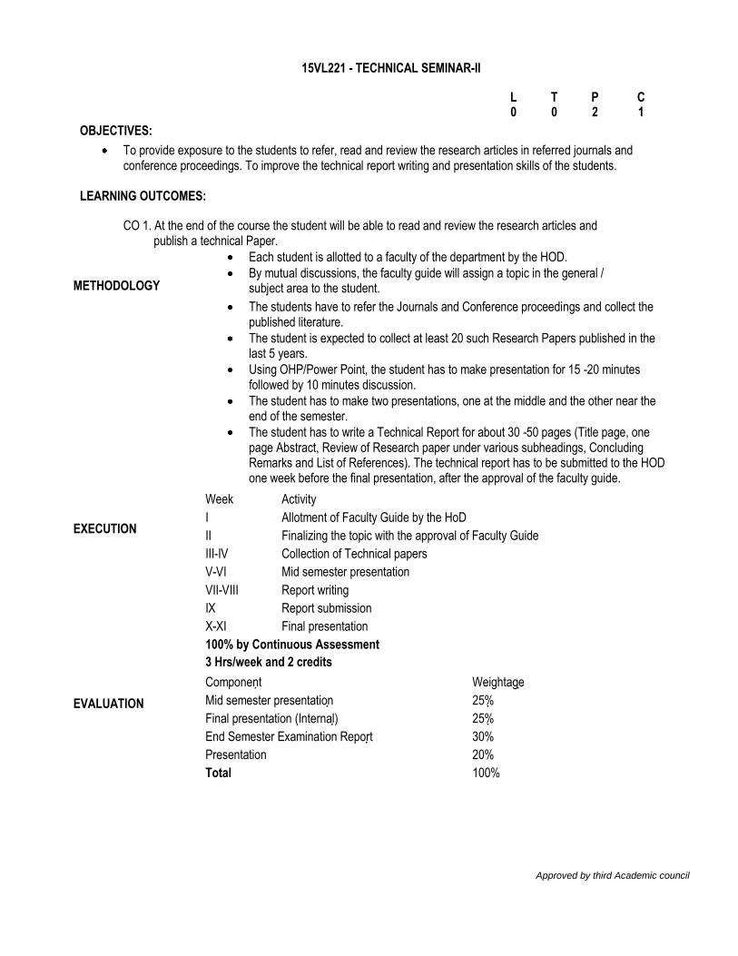
15VL121 - TECHNICAL SEMINAR-I
L T P C 0 0 2 1
OBJECTIVES:
To provide exposure to the students to refer, read and review the research articles in referred journals and conference proceedings. To improve the technical report writing and presentation skills of the students.
LEARNING OUTCOMES:
CO 1. At the end of the course the student will be able to read and review the research articles and publish a technical Paper.
METHODOLOGY
METHODOLOGY
Each student is allotted to a faculty of the department by the HOD.
By mutual discussions, the faculty guide will assign a topic in the general / subject area to the student.
The students have to refer the Journals and Conference proceedings and collect the published literature.
The student is expected to collect at least 20 such Research Papers published in the last 5 years.
Using OHP/Power Point, the student has to make presentation for 15 -20 minutes followed by 10 minutes discussion.
The student has to make two presentations, one at the middle and the other near the end of the semester.
The student has to write a Technical Report for about 30 -50 pages (Title page, one page Abstract, Review of Research paper under various subheadings, Concluding Remarks and List of References). The technical report has to be submitted to the HOD one week before the final presentation, after the approval of the faculty guide.
EXECUTION
EXECUTION
Week Activity
I Allotment of Faculty Guide by the HoD
II Finalizing the topic with the approval of Faculty Guide
III-IV Collection of Technical papers
V-VI Mid semester presentation
VII-VIII Report writing
IX Report submission
X-XI Final presentation
EVALUATION
EVALUATION
100% by Continuous Assessment
3 Hrs/week and 2 credits
Component Weightage
Mid semester presentation 25%
Final presentation (Internal) 25%
End Semester Examination Report 30%
Presentation 20%
Total 100%

Approved by third Academic council
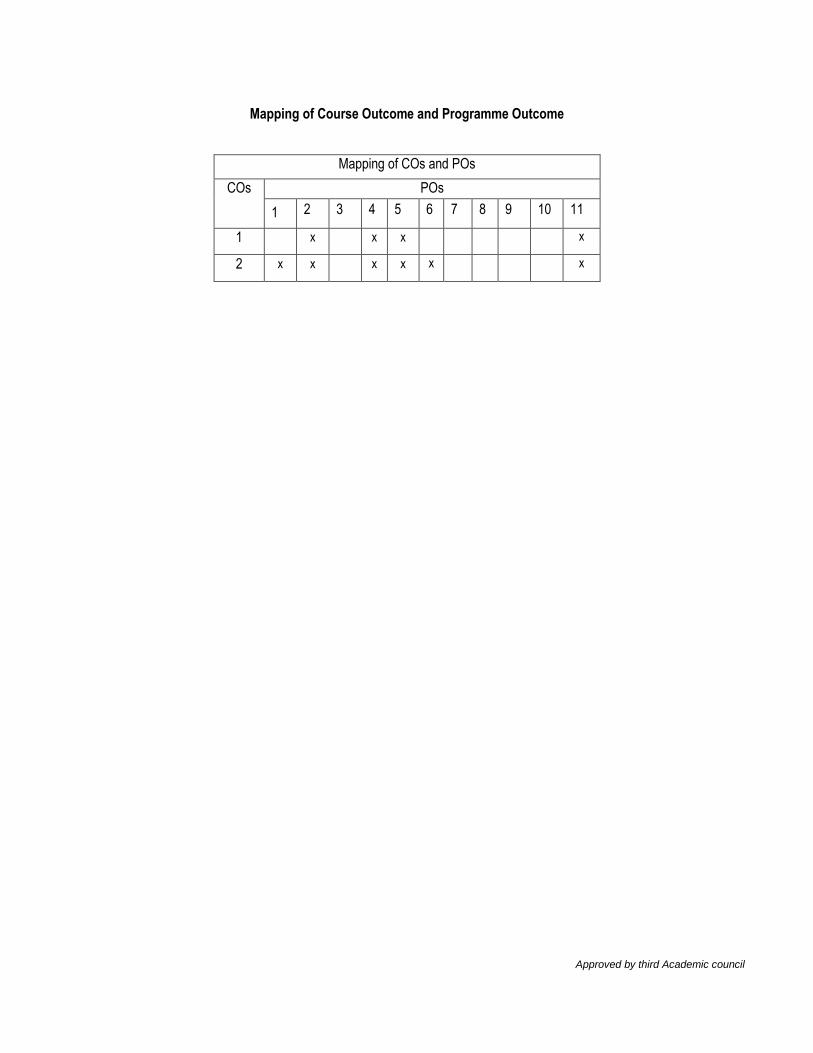
Mapping of Course Outcome and Programme Outcome
Mapping of COs and POs
COs POs
1 2 3 4 5 6 7 8 9 10 11
1 × × × × × ×

Approved by third Academic council
15AE201 ANALYSIS AND DESIGN OF ANALOG INTEGRATED CIRCUITS
L T P C 3 0 0 3 OBJECTIVES:
To design the single stage amplifiers using PMOS and NMOS driver circuits with different loads.
To analyze high frequency concepts of single stage amplifiers and noise characteristics associated with differential amplifiers.
To study the different types of current mirrors and to know the concepts of voltage and current reference circuits.
LEARNING OUTCOMES: On completion of this course the student will be able to
CO1. Analyze the bias circuit using CMOS current mirror. CO2. Design feedback and differential operational amplifier. CO3. Analyze stability of operational amplifiers. CO4. Apply frequency compensation techniques for Amplifiers .
UNIT I - MODELS FOR INTEGRATED CIRCUIT ACTIVE DEVICES (9) Depletion region of a pn junction – large signal behavior of bipolar transistors- small signal model of bipolar transistor- large signal behavior of MOSFET- small signal model of the MOS transistors- short channel effects in MOS transistors – weak inversion in MOS transistors- substrate current flow in MOS transistor. UNIT II - CIRCUIT CONFIGURATION FOR LINEAR IC (9) Current sources, Analysis of difference amplifiers with active load using BJT and FET, supply and temperature independent biasing techniques, voltage references. Output stages: Emitter follower, source follower and Push pull output stages. UNIT III - OPERATIONAL AMPLIFIERS (9) Analysis of operational amplifiers circuit, slew rate model and high frequency analysis, Frequency response of integrated circuits: Single stage and multistage amplifiers, Operational amplifier noise. UNIT IV - ANALOG MULTIPLIER AND PLL (9) Analysis of four quadrant and variable trans conductance multiplier, voltage controlled oscillator, closed loop analysis of PLL, Monolithic PLL design in integrated circuits: Sources of noise- Noise models of Integrated-circuit Components – Circuit Noise Calculations – Equivalent Input Noise Generators – Noise Bandwidth – Noise Figure and Noise Temperature. UNIT V - ANALOG DESIGN WITH MOS TECHNOLOGY (9) MOS Current Mirrors – Simple, Cascode, Wilson and Widlar current source – CMOS Class AB output stages – Two stage MOS Operational Amplifiers, with Cascode, MOS Telescopic-Cascode Operational Amplifier – MOS Folded Cascode and MOS Active Cascode Operational Amplifiers.
TOTAL = 45 PERIODS

Approved by third Academic council
REFERENCES: 1. Gray, Meyer, Lewis, Hurst, “Analysis and design of Analog IC‟s”, 4th Edition, Wiley International,2002 2. Behzad Razavi, “Design of Analog CMOS Integrated Circuits”, S.Chand and company ltd, 2000
3. Nandita Dasgupata, Amitava Dasgupta,”Semiconductor Devices,Modelling and Technology”, Prentice Hall of Indiapvt.ltd,2004.
4. Grebene, Bipolar and MOS Analog Integrated circuit design”, John Wiley & sons,Inc.,2003.
5. Phillip E.Allen Douglas R. Holberg, “CMOS Analog Circuit Design”, Second Edition-Oxford University Press-2003
Mapping of Course Outcome and Programme Outcome
Mapping of COs and POs
COs POs
1 2 3 4 5 6 7 8 9 10 11
1 x x x x x
2 x x x x x
3 x x x x x x
4 x x x x x

Approved by third Academic council
15VL201 CAD FOR VLSI CIRCUITS
L T P C 3 0 0 3
OBJECTIVES:
To discuss the basics of VLSI Design Automation.
To understand the concepts of physical design process
To gain the knowledge on Simulation and Synthesis in VLSI Design Automation.
LEARNING OUTCOMES:
At the end of the course the students will be able to CO1.Design advanced electronics systems CO2.Evaluate and analyze the systems in VLSI design environments. CO3.Apply advanced technical knowledge in multiple contexts CO4.Conduct an organized and systematic study on significant research topic within the field of VLSI and its allied field.
UNIT I - VLSI DESIGN METHODOLOGIES (9) Introduction to VLSI Design methodologies - Review of Data structures and algorithms - Review of VLSI Design automation tools - Algorithmic Graph Theory and Computational Complexity -Tractable and Intractable problems - general purpose methods for combinatorial optimization.
UNIT II-DESIGN RULES (9)
Layout Compaction - Design rules - problem formulation - algorithms for constraint graph compaction - placement and partitioning – Circuit representation – Placement algorithms -partitioning. UNIT III:FLOOR PLANNING (9) Floor planning concepts - shape functions and floorplan sizing - Types of local routing problems -Area routing - channel routing - global routing - algorithms for global routing.
UNIT IV:SIMULATION (9) Simulation - Gate-level modeling and simulation - Switch-level modeling and simulation -Combinational Logic Synthesis - Binary Decision Diagrams - Two Level Logic Synthesis.
UNIT V:MODELLINGAND SYNTHESIS (9) High level Synthesis - Hardware models - Internal representation - Allocation - assignment and scheduling - Simple scheduling algorithm – Assignment problem–High level transformations.
TOTAL: 45 PERIODS
REFERENCES:
1. S.H. Gerez, "Algorithms for VLSI Design Automation", John Wiley & Sons,2002. 2. N.A. Sherwani, "Algorithms for VLSI Physical Design Automation", Kluwer Academic Publishers, 2002.

Approved by third Academic council
Mapping of Course Outcome and Programme Outcome
Mapping of COs and POs
COs POs
1 2 3 4 5 6 7 8 9 10 11
1 X X X X X X
2 X X X X X
3 X X X X X X X
4 X X X X X X X
Approved by third Academic council
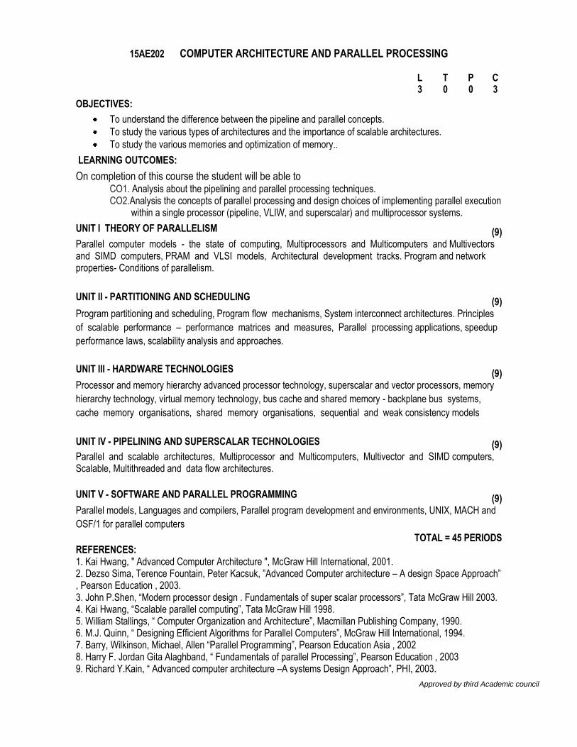
15AE202 COMPUTER ARCHITECTURE AND PARALLEL PROCESSING
L T P C 3 0 0 3
OBJECTIVES:
To understand the difference between the pipeline and parallel concepts.
To study the various types of architectures and the importance of scalable architectures.
To study the various memories and optimization of memory..
LEARNING OUTCOMES:
On completion of this course the student will be able to CO1. Analysis about the pipelining and parallel processing techniques. CO2.Analysis the concepts of parallel processing and design choices of implementing parallel execution within a single processor (pipeline, VLIW, and superscalar) and multiprocessor systems.
UNIT I THEORY OF PARALLELISM (9) Parallel computer models - the state of computing, Multiprocessors and Multicomputers and Multivectors and SIMD computers, PRAM and VLSI models, Architectural development tracks. Program and network properties- Conditions of parallelism.
UNIT II - PARTITIONING AND SCHEDULING (9)
Program partitioning and scheduling, Program flow mechanisms, System interconnect architectures. Principles
of scalable performance – performance matrices and measures, Parallel processing applications, speedup
performance laws, scalability analysis and approaches.
UNIT III - HARDWARE TECHNOLOGIES (9) Processor and memory hierarchy advanced processor technology, superscalar and vector processors, memory
hierarchy technology, virtual memory technology, bus cache and shared memory - backplane bus systems,
cache memory organisations, shared memory organisations, sequential and weak consistency models
UNIT IV - PIPELINING AND SUPERSCALAR TECHNOLOGIES (9) Parallel and scalable architectures, Multiprocessor and Multicomputers, Multivector and SIMD computers, Scalable, Multithreaded and data flow architectures.
UNIT V - SOFTWARE AND PARALLEL PROGRAMMING (9) Parallel models, Languages and compilers, Parallel program development and environments, UNIX, MACH and
OSF/1 for parallel computers
TOTAL = 45 PERIODS REFERENCES: 1. Kai Hwang, " Advanced Computer Architecture ", McGraw Hill International, 2001. 2. Dezso Sima, Terence Fountain, Peter Kacsuk, ”Advanced Computer architecture – A design Space Approach” , Pearson Education , 2003. 3. John P.Shen, “Modern processor design . Fundamentals of super scalar processors”, Tata McGraw Hill 2003. 4. Kai Hwang, “Scalable parallel computing”, Tata McGraw Hill 1998. 5. William Stallings, “ Computer Organization and Architecture”, Macmillan Publishing Company, 1990. 6. M.J. Quinn, “ Designing Efficient Algorithms for Parallel Computers”, McGraw Hill International, 1994. 7. Barry, Wilkinson, Michael, Allen “Parallel Programming”, Pearson Education Asia , 2002 8. Harry F. Jordan Gita Alaghband, “ Fundamentals of parallel Processing”, Pearson Education , 2003 9. Richard Y.Kain, “ Advanced computer architecture –A systems Design Approach”, PHI, 2003.

Approved by third Academic council
Mapping of Course Outcome and Programme Outcome
Mapping of COs and POs
COs POs
1 2 3 4 5 6 7 8 9 10 11
1 x x x x x x x
2 x x x x

Approved by third Academic council
15AE204 ADVANCED EMBEDDED SYSTEMS
L T P C 3 0 0 3
OBJECTIVES:
To afford awareness about Hardware and software design architecture for embedded processors With real time examples.
To acquire sound knowledge about ARM processors and SHARC processor cores
To understand the concept of embedded Architecture and emphasis the knowledge of various processors and embedded networking.
To study various real time Embedded algorithms
To learn various techniques of system design Technique.
LEARNING OUTCOMES:
On completion of this course the student will be able to
CO1. Know about various Requirements, Specification and Architectural Design for Embedded system design process. CO2. Understand and apply interfacing concepts of SHARC and ARM processors. CO3. Realize concepts about various Embedded Network using I2C, CAN Bus and SHARC bus for industry based applications. CO4. Apply the programming skills for peripheral interfacing and real time applications. CO5. Apply the concepts of RTOS for real-time systems design.
UNIT I EMBEDDED PROCESSORS (9) Embedded Computers, Characteristics of Embedded Computing Applications, Challenges in Embedded Computing system design, Embedded system design process-Requirements, Specification, Architectural Design, Designing Hardware and Software Components, System Integration, Formalism for System Design- Structural Description, Behavioral Description, Design Example: Model Train Controller.
UNIT II - EMBEDDED PROCESSOR AND COMPUTING PLATFORM (9)
ARM processor- processor and memory organization. Data operations, Flow of Control, SHARC processor- Memory organization, Data operations, Flow of Control, parallelism with instructions, CPU Bus configuration, ARM Bus, SHARC Bus, Memory devices, Input/output devices, Component interfacing, designing with microprocessor development and debugging, Design Example : Alarm Clock. Hybrid Architecture.
UNIT III - NETWORKS (9) Distributed Embedded Architecture- Hardware and Software Architectures, Networks for embedded systems- I2C, CAN Bus, SHARC link supports, Ethernet, Myrinet, Internet, Network-Based design- Communication Analysis, system performance Analysis, Hardware platform design, Allocation and scheduling, Design Example: Elevator Controller
UNIT IV - REAL-TIME SCHEDULING ALGORITHMS (9) Clock driven Approach, weighted round robin Approach, Priority driven Approach, Dynamic Versus Static systems, effective release times and deadlines, Optimality of the Earliest deadline first (EDF) algorithm, challenges in validating timing constraints in priority driven systems, Off-line Versus On-line scheduling.
UNIT V - SYSTEM DESIGN TECHNIQUES (9) Design Methodologies, Requirement Analysis, Specification, System Analysis and Architecture Design, Quality Assurance, Design Example: Home Automation- System Architecture, Laser jet printer- Hardware Design and Software Design, Video conferencing, Set-top Boxes.
TOTAL = 45 PERIODS

Approved by third Academic council
REFERENCES: 1.Wayne Wolf, ―Computers as Components: Principles of Embedded Computing System Design, Morgan Kaufman Publishers. 2005 2. Jane.W.S. Liu, ―Real-Time systems, Pearson Education Asia. 2000 3. C. M. Krishna and K. G. Shin, ―Real-Time Systems, McGraw-Hill, 1997 4. Frank Vahid and Tony Givargis, ―Embedded System Design: A Unified Hardware/Software Introduction , John Wiley & Sons.2003
Mapping of Course Outcome and Programme Outcome
Mapping of COs and POs
COs POs
1 2 3 4 5 6 7 8 9 10 11
1 × × × × × ×
2 × × × × ×
3 × × × × × ×
4 × × × × × ×
5 × × × × × ×

Approved by third Academic council
15VL211 VLSI DESIGN LAB II
L T P C 0 0 4 2
OBJECTIVES:
To learn about digital system design and their implementation in FPGA devices
To learn about implementation Embedded systems using different target devices
To have analysis knowledge by SPICE tool
To learn about layout level design of digital systems in transistor level
LEARNING OUTCOMES:
On completion of this course the students will be able to CO1. Have knowledge about digital system design and implementation in FPGAs CO2. Have analysis knowledge of various parameters by T-SPICE tool CO3. Design and implement the Embedded systems. CO4. Have knowledge of layout level design entries
1. Implementation of the Device control system in FPGA. 2. Implementation of the Elevator controller using 89C51 microcontroller 3. Implementation of the Message Displaying system using PIC microcontroller. 4. Implementation of the ZIGBEE RF communication system using ARM microcontroller. 5. Implementation of the stepper motor control using FPGA. 6. Implementation of the DC motor control using FPGA. 7. Layout level design of CMOS Inverter & NAND Gate.
TOTAL: L: 60 = 60 PERIODS
Mapping of Course Outcome and Programme Outcome
Mapping of COs and POs
COs POs
1 2 3 4 5 6 7 8 9 10 11
1 x x x x
2 x x x x
3 x x x x x x
4 x x x x
Approved by third Academic council
15VL221 - TECHNICAL SEMINAR-II
L T P C 0 0 2 1
OBJECTIVES:
To provide exposure to the students to refer, read and review the research articles in referred journals and conference proceedings. To improve the technical report writing and presentation skills of the students.
LEARNING OUTCOMES:
CO 1. At the end of the course the student will be able to read and review the research articles and publish a technical Paper.
METHODOLOGY
METHODOLOGY
Each student is allotted to a faculty of the department by the HOD.
By mutual discussions, the faculty guide will assign a topic in the general / subject area to the student.
The students have to refer the Journals and Conference proceedings and collect the published literature.
The student is expected to collect at least 20 such Research Papers published in the last 5 years.
Using OHP/Power Point, the student has to make presentation for 15 -20 minutes followed by 10 minutes discussion.
The student has to make two presentations, one at the middle and the other near the end of the semester.
The student has to write a Technical Report for about 30 -50 pages (Title page, one page Abstract, Review of Research paper under various subheadings, Concluding Remarks and List of References). The technical report has to be submitted to the HOD one week before the final presentation, after the approval of the faculty guide.
EXECUTION
EXECUTION
Week Activity
I Allotment of Faculty Guide by the HoD
II Finalizing the topic with the approval of Faculty Guide
III-IV Collection of Technical papers
V-VI Mid semester presentation
VII-VIII Report writing
IX Report submission
X-XI Final presentation
EVALUATION
EVALUATION
100% by Continuous Assessment
3 Hrs/week and 2 credits
Component Weightage
Mid semester presentation 25%
Final presentation (Internal) 25%
End Semester Examination Report 30%
Presentation 20%
Total 100%

Approved by third Academic council
Mapping of Course Outcome and Programme Outcome
Mapping of COs and POs
COs POs
1 2 3 4 5 6 7 8 9 10 11
1 × × × × × ×

Approved by third Academic council
15AE104 ADVANCED MICROPROCESSORS AND MICROCONTROLLERS
L T P C 3 0 0 3
OBJECTIVES:
To familiarize the fundamental concepts of microprocessor architecture.
To gain knowledge about high performance CISC and RISC architectures.
To acquire sound knowledge about ARM processors and CPU cores.
To study about 8 bit Microcontrollers viz. 68HC11 and PIC.
To understand the concepts of 16 bit MSP430 Microcontroller architecture.
LEARNING OUTCOMES:
On completion of this course the student will be able to CO1. Understand concepts about various CISC and RISC processors architecture.
CO2. Apply the programming skills for peripheral interfacing and real time applications. CO3 Diagnose the design and methodologies in hardware and software design. CO4. Apply the concepts of RTOS for system design.
UNIT I HIGH PERFORMANCE CISC ARCHITECTURE – PENTIUM (9) CPU Architecture- Bus Operations – Pipelining – Brach predication – floating point unit-Operating Modes –Paging – Multitasking – Exception and Interrupts – Instruction set –addressing modes – Programming the Pentium processor.
UNIT II - HIGH PERFORMANCE RISC ARCHITECTURE: ARM (9)
The RISC revolution-The reduced instruction set computer –Design for low power consumption- The ARMarchitecture basics-Architectural inheritance-The ARM programmers model-ARM organization and implementation-3 stage and 5 stage pipeline ARM organization- ARM instruction execution-ARMimplementation-ARM processor cores-ARM7 TDMI-ARM8 TDMI-ARM9 TDMI- ARM development tools-Architecturalsupport for system development
UNIT III - ARM INSTRUCTION AND ASSEMBLY LANGUAGE PROGRAMMING (9) Exceptions-Conditional execution-Branch and branch with link and exchange-Software interrupt- Data processing instructions-Single word and unsigned byte data transfer and half word and signed byte data transfer instructions-Multiple register transfer instructions-Swap instructions-Architectural support for high level languages-The thumb instruction set-Thumb implementation-Thumb applications-Writing simple assembly language programs.
UNIT IV - PIC MICROCONTROLLER (9) CPU Architecture – Instruction set – interrupts- Timers- I2C Interfacing – UART- A/D Converter –PWM and introduction to C-Compilers
UNIT V - MSP430 MICROCONTROLLER (9) Architecture of the MSP430 : Central Processing unit- Addressing modes – Constant generator and emulated instruction – Instruction Set – Resets– Clock System Function and subroutine – Interrupts – Low Power modes of Operation – Watch dog timer -Serial peripheral Interface
TOTAL = 45 PERIODS

Approved by third Academic council
REFERENCES: 1. James L. Antonakos, “The Pentium Microprocessor „‟ Pearson Education, 1997. 2. Steve Furber, „‟ ARM System –On –Chip architecture “Addison Wesley, 2000. 3. John .B.Peatman, “Design with PIC Microcontroller, Prentice hall, 1997. 4. John davies ” MSP430 MICROCONTROLLER basics”Elsevier,2008
Mapping of Course Outcome and Programme Outcome
Mapping of COs and POs
COs POs
1 2 3 4 5 6 7 8 9 10 11
1 × × × × × ×
2 × × × × × × ×
3 × × × × ×
4 × × × × × ×

Approved by third Academic council
15AEX07 ANALOG VLSI DESIGN L T P C 3 0 0 3
OBJECTIVES:
To study the concepts of CMOS and BICMOS analog circuits.
To understand the concepts of A/D convertors.
To understand the testing concepts in analog VLSI circuits and its statistical modeling.
To understand the different types of layout design.
LEARNING OUTCOMES:
On completion of this course the student will be able to
CO1. Learn the basics of CMOS and BICMOS circuit techniques. CO2. Gain a well founded knowledge on filters and converters. CO3. Obtain knowledge on testability and VLSI interconnects. CO4. Grasp the concept of statistical modeling and simulation.
UNIT I BASIC CMOS CIRCUIT TECHNIQUES (9) Mixed-Signal VLSI Chips-Basic CMOS Circuits-Basic Gain Stage- Gain Boosting Techniques - Super MOS Transistor- Primitive Analog Cells-Linear Voltage-Current Converters-MOS Multipliers and Resistors-CMOS - Bipolar and Low-Voltage BiCMOS OpAmp Design- Instrumentation Amplifier Design.
UNIT II - CURRENT -MODE SIGNAL PROCESSING AND NEURAL INFORMATION PROCESSING (9)
Continuous-Time Signal Processing-Sampled-Data Signal Processing-Switched-Current Data Converters-Practical Considerations in SI Circuits Biologically-Inspired Neural Networks Floating - Gate, Low-Power Neural Networks- CMOS Technology and Models- Design Methodology-Networks-Contrast Sensitive Silicon Retina.
UNIT III - SAMPLED DATA ANALOG FILTERS (9) First-order and Second SC Circuits-Bilinear Transformation - Cascade Design-Switched-Capacitor Ladder Filter-Synthesis of Switched-Current Filter- Nyquist rate A/D Converters-Modulators for Over sampled A/D Conversion-First and Second Order and Multibit Sigma-Delta Modulators-Interpolative Modulators Cascaded Architecture-Decimation Filters.
UNIT IV - DESIGN FOR TESTABILITY (9) Fault modeling and Simulation - Testability-Analysis Technique-Ad Hoc Methods and General Guidelines-Scan Techniques- Boundary Scan-Built-in Self Test-Analog Test Buses-Design for Electron -Beam Testability-Physics of Interconnects in VLSI-Scaling of Interconnects.
UNIT V - STATISTICAL MODELING AND SIMULATION (9) Review of Statistical Concepts - Statistical Device Modeling- Statistical Circuit Simulation-Automation Analog Circuit Design-automatic Analog Layout-CMOS Transistor Layout-Resistor Layout-Capacitor Layout-Analog Cell Layout-Mixed Analog - Digital Layout.
TOTAL = 45 PERIODS

Approved by third Academic council
REFERENCES: 1. Mohammed Ismail, Terri Fiez, “Analog VLSI signal and Information Processing”, McGraw-Hill
International Editions, 1994. 2. Malcom R.Haskard, Lan C.May, “Analog VLSI Design - NMOS and CMOS “, Prentice Hall, 1998. 3. Randall L Geiger, Phillip E. Allen, “ Noel K.Strader, VLSI Design Techniques for Analog and Digital Circuits “, Mc Graw Hill International Company, 1990. 4. Jose E.France, Yannis Tsividis, “ Design of Analog-Digital VLSI Circuits for Telecommunication and Signal Processing “, Prentice Hall, 1994
Mapping of Course Outcome and Programme Outcome
Mapping of COs and POs
COs POs
1 2 3 4 5 6 7 8 9 10 11
1 X X X
2 X X X X X X X
3 X X X X X X X
4 X X X X X X X
Approved by third Academic council
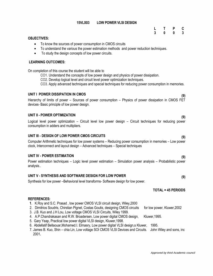
15VLX03 LOW POWER VLSI DESIGN
L T P C 3 0 0 3
OBJECTIVES:
To know the sources of power consumption in CMOS circuits
To understand the various the power estimation methods and power reduction techniques.
To study the design concepts of low power circuits.
LEARNING OUTCOMES: On completion of this course the student will be able to
CO1. Understand the concepts of low power design and physics of power dissipation. CO2. Develop logical level and circuit level power optimization techniques. CO3. Apply advanced techniques and special techniques for reducing power consumption in memories.
UNIT I POWER DISSIPATION IN CMOS (9) Hierarchy of limits of power – Sources of power consumption – Physics of power dissipation in CMOS FET devices- Basic principle of low power design.
UNIT II - POWER OPTIMIZATION (9)
Logical level power optimization – Circuit level low power design – Circuit techniques for reducing power consumption in adders and multipliers.
UNIT III - DESIGN OF LOW POWER CMOS CIRCUITS (9) Computer Arithmetic techniques for low power systems – Reducing power consumption in memories – Low power clock, Interconnect and layout design – Advanced techniques – Special techniques
UNIT IV - POWER ESTIMATION (9) Power estimation techniques – Logic level power estimation – Simulation power analysis – Probabilistic power analysis..
UNIT V - SYNTHESIS AND SOFTWARE DESIGN FOR LOW POWER (9) Synthesis for low power –Behavioral level transforms- Software design for low power.
TOTAL = 45 PERIODS
REFERENCES: 1. K.Roy and S.C. Prasad , low power CMOS VLSI circuit design, Wiley,2000
2. Dimitrios Soudris, Chirstian Pignet, Costas Goutis, designing CMOS circuits for low power, Kluwer,2002 3. J.B. Kuo and J.H Lou, Low voltage CMOS VLSI Circuits, Wiley 1999. 4. A.P.Chandrakasan and R.W. Broadersen, Low power digital CMOS design, Kluwer,1995. 5. Gary Yeap, Practical low power digital VLSI design, Kluwer,1998. 6. Abdellatif Bellaouar,Mohamed.I. Elmasry, Low power digital VLSI design,s Kluwer, 1995. 7. James B. Kuo, Shin – chia Lin, Low voltage SOI CMOS VLSI Devices and Circuits. John Wiley and sons, inc 2001.

Approved by third Academic council
Mapping of Course Outcome and Programme Outcome
Mapping of COs and POs
COs POs
1 2 3 4 5 6 7 8 9 10 11
1 × × × × × × ×
2 × × × × × ×
3 × × × × × ×

Approved by third Academic council
15VLX04 PHYSICAL DESIGN OF VLSI CIRCUITS
L T P C 3 0 0 3
OBJECTIVES:
To familiarize the fundamental concepts of routing.
To gain knowledge about circuit layouts.
LEARNING OUTCOMES:
On completion of this course students will be able to
CO1. Design the circuit layouts by analyzing the performance issues of circuits.
CO2. Solve practical engineering problems pertaining to the field of VLSI designs.
UNIT I - INTRODUCTION TO VLSI DESIGN SYNTHESIS (9) Hardware models - Internal representation - Allocation assignment and scheduling - Simple scheduling algorithm - Algorithmic Paradigms.
UNIT II - PLACEMENT AND FLOOR PLANNING (9)
Floor planning: Rectangular dual floor planning- hierarchical approach- Floor plan sizing. Placement: Cost function-regular placement - linear placement
UNIT III - PARTITIONING AND ROUTING (9) Partitioning: Ratio cut- Partitioning with capacity and I/O constraints- Partitioning Placement. Global Routing: Sequential Approaches- hierarchical approaches. Detailed Routing: Channel routing - Switch box routing. Routing in FPGA: Array based FPGA- Row based FPGAs.
UNIT IV - LAYOUT COMPACTION AND PERFORMANCE ISSUES IN CIRCUIT LAYOUT (9) Layout: 1D compaction- 2D compaction. Delay Models: Gate Delay Models- Models for interconnected Delay- Delay in RC trees. Timing Driven Placement: Zero Stack Algorithm- Weight based placement. Minimization: constrained via Minimization-unconstrained via Minimization.
UNIT V - SINGLE LAYER ROUTING AND LOGIC SYNTHESIS (9) Wire length and bend minimization technique–Over the Cell (OTC) Routing – Introduction to Combinational Logic Synthesis - Binary Decision Diagrams - Two Level Logic Synthesis.
TOTAL= 45 PERIODS REFERENCES:
1. Sarafzadeh, C.K. Wong, ―An Introduction to VLSI Physical Design‖ , Mc Graw Hill
International Edition 1995 2. Preas M. Lorenzatti, ― Physical Design and Automation of VLSI systems‖ , The Benjamin Cummins
Publishers, 1998. 3. H.Gerez, Algorithms for VLSI Design Automation, John Wiley & Sons, 2002
4. N.A Sherwani, Algorithms for VLSI Physical Design Automation, Kluwer Academic Publishers, 2002.
5. R .Drechsler, Evolutionary Algorithms for VLSI CAD, Boston, Kluwer Academic Publishers, 2010. 6. D.Hill, D.Shugard, J.Fishburn and K.Keutzer, Algorithms and Techniques for VLSI Layout Synthesis,
Kluwer Academic Publishers, Boston, 1990.
Approved by third Academic council
Mapping of Course Outcome and Programme Outcome
Mapping of COs and POs
COs POs
1 2 3 4 5 6 7 8 9 10 11
1 x x x x
2 x x x x x x

Approved by third Academic council
15VLX05 VLSI TECHNOLOGY
L T P C 3 0 0 3
OBJECTIVES:
To understand the Fabrication of ICs and purification of Silicon in different technologies.
To impart in-depth knowledge about Etching and deposition of different layers.
To understand the different packaging techniques of VLSI devices.
To learn methodology for IC fabrication and to learn various techniques are diffusion, ion implantation, Oxidation, epitaxy, etching, lithography for circuit fabrication.
LEARNING OUTCOMES: On completion of this course the student will be able
CO1. To use metallization techniques to create three-dimensional device structures and devices. CO2 . To know methodology to fabricate an IC‟s.
UNIT I CRYSTAL GROWTH, WAFER PREPARATION, EPITAXY AND OXIDATION (9)
Electronic Grade Silicon, Czochralski crystal growing, Silicon Shaping, processing consideration, Vapor phase Epitaxy, Molecular Beam Epitaxy, Silicon on Insulators, Epitaxial Evaluation, Growth Mechanism and kinetics, Thin Oxides, Oxidation Techniques and Systems, Oxide properties, Redistribution of Dopants at interface, Oxidation of Poly Silicon, Oxidation induced Defects.
UNIT II LITHOGRAPHY AND RELATIVE PLASMA ETCHING (9)
Optical Lithography, Electron Lithography, X-Ray Lithography, Ion Lithography, Plasma properties, Feature Size control and Anisotropic Etch mechanism, relative Plasma Etching techniques and Equipments
UNIT III DEPOSITION, DIFFUSION, ION IMPLEMENTATION AND METALISATION (9) Deposition process, Polysilicon, plasma assisted Deposition, Models of Diffusion in Solids, Flick‟s one
dimensional Diffusion Equation – Atomic Diffusion Mechanism – Measurement techniques - Range theory-
Implant equipment. Annealing Shallow junction – High energy implantation – Physical vapour deposition –
Patterning.
UNIT IV PROCESS SIMULATION AND VLSI PROCESS INTEGRATION (9) Ion implantation – Diffusion and oxidation – Epitaxy – Lithography – Etching and Deposition- NMOS IC Technology – CMOS IC Technology – MOS Memory IC technology - Bipolar IC Technology – IC Fabrication.
UNIT V ASSEMBLY TECHNIQUES AND PACKAGING OF VLSI DEVICES (9) Analytical Beams – Beams Specimen interactions - Chemical methods – Package types – banking design
consideration – VLSI assembly technology – Package fabrication technology.
TOTAL= 45 PERIODS REFERENCES:
1. S.M.Sze, “VLSI Technology”, Mc.Graw.Hill Second Edition. 2002. 2. Amar Mukherjee, “Introduction to NMOS and CMOS VLSI System design Prentice Hall India.2000. 3. W. Wolf, Modern VLSI Design, third edition, Pearson Publication,2002 4. Wai Kai Chen, VLSI Technology, CRC press, 2003.

Approved by third Academic council
Mapping of Course Outcome and Programme Outcome
Mapping of COs and POs
COs POs
1 2 3 4 5 6 7 8 9 10 11
1 x x x x x
2 x x x x x

Approved by third Academic council
15VLX06 ASIC DESIGN
L T P C 3 0 0 3
OBJECTIVES:
To study the design flow of different types of ASIC.
To familiarize the different types of programming technologies and logic devices.
To learn the architecture of different types of FPGA.
To gain knowledge about partitioning, floor planning, placement and routing including circuit extraction of ASIC
To know about synthesis, Simulation and testing of systems.
To understand the design issues of SOC.
LEARNING OUTCOMES:
On completion of this course the student will be able to CO1. Understand the basics of ASIC design flow and library design. CO2. Gain a well founded knowledge of logical cells and i/o cells. CO3. Apply various logic synthesis techniques, simulation and testing in digital system design. CO4. Implement the ASIC construction, floor planning, placement and routing. CO4. Design and develop high performance algorithms and its applications in ASICs.
UNIT I INTRODUCTION TO ASICS, CMOS LOGIC AND ASIC LIBRARY DESIGN (9)
Types of ASICs - Design flow -CMOS transistors - Combinational Logic Cell – Sequential logic cell - Data path logic cell - Transistors as Resistors - Transistor Parasitic Capacitance- Logical effort.
UNIT II PROGRAMMABLE ASICS, PROGRAMMABLE ASIC LOGIC CELLS AND PROGRAMMABLE ASIC I/O CELLS
(9) Anti fuse - static RAM - EPROM and EEPROM technology - Actel ACT - Xilinx LCA –Altera FLEX - Altera MAX DC & AC inputs and outputs - Clock & Power inputs - Xilinx I/O blocks
UNIT III - PROGRAMMABLE ASIC INTERCONNECT, PROGRAMMABLE ASIC DESIGN SOFTWARE AND LOW LEVEL DESIGN ENTRY
(9) Actel ACT -Xilinx LCA - Xilinx EPLD - Altera MAX 5000 and 7000 - Altera MAX9000 - Altera FLEX –Design systems - Half gate ASIC –Schematic entry -Low level design language - PLA tools -EDIF- CFI design representation.
UNIT IV - LOGIC SYNTHESIS, SIMULATION AND TESTING (9)
Verilog and logic synthesis -VHDL and logic synthesis - types of simulation -boundary scan test - fault simulation - automatic test pattern generation.
UNIT V - ASIC CONSTRUCTION, FLOOR PLANNING, PLACEMENT AND ROUTING (9)
System partition - FPGA partitioning - partitioning methods - floor planning - placement -physical design flow –global routing - detailed routing - special routing - circuit extraction –DRC
TOTAL = 45 PERIODS REFERENCES: 1. M.J.S.Smith, " Application - Specific Integrated Circuits", Pearson,2003 2. Farzad Nekoogar and Faranak Nekoogar, From ASICs to SOCs: A Practical Approach, Prentice Hall PTR, 2003 3. Wayne Wolf, FPGA-Based System Design, Prentice Hall PTR, 2004. 4. R. Rajsuman, System-on-a-Chip Design and Test. Santa Clara, CA: Artech House Publishers, 2000. 5. F. Nekoogar. Timing Verification of Application-Specific Integrated Circuits (ASICs).Prentice Hall PTR, 1999

Approved by third Academic council
Mapping of Course Outcome and Programme Outcome
Mapping of COs and POs
COs POs
1 2 3 4 5 6 7 8 9 10 11
1 × × × × ×
2 × × × × ×
3 × × × × × ×
4 × × × × × ×
5 × × × × ×

Approved by third Academic council
15VLX07 TESTING OF VLSI CIRCUITS
L T P C 3 0 0 3
OBJECTIVES:
To have knowledge about various faults and modeling of the faults in digital systems.
To learn about various methods to detect the faults in combinational and sequential systems.
To provide knowledge about designing of Testable system designs
LEARNING OUTCOMES:
On completion of this course the students will be able to CO1. Detect faults occurring in digital systems and modelling of the faults to simplifying the detection CO2. Generate test vectors to detect and diagnose the faults using various algorithms CO3. Design testable Combinational and Sequential circuits CO4. Design testable memory units
UNIT I BASICS OF TESTING AND FAULT MODELLING (9)
Introduction to testing – Faults in Digital Circuits – Modelling of faults – Logical Fault Models – Fault detection – Fault Location – Fault dominance – Logic simulation – Types of simulation – Delay models – Gate Level Event – driven simulation.
UNIT II - TEST GENERATION FOR COMBINATIONAL CIRCUITS (9)
Test generation for combinational logic circuits – Testable combinational logic circuit design .
UNIT III - TEST GENERATION FOR SEQUENTIAL & DFT (9)
Test generation for sequential circuits – design of testable sequential circuits Design for Testability – Ad-hoc design – system level DFT approaches.
UNIT IV - SELF – TEST AND TEST ALGORITHMS (9)
Built-In self Test – test pattern generation for BIST – Circular BIST – BIST Architectures – Testable Memory Design – Test Algorithms – Test generation for Embedded RAMs.
UNIT V - FAULT DIAGNOSIS (9)
Logical Level Diagnosis – Diagnosis by UUT reduction – Fault Diagnosis for Combinational Circuits – Self-checking design.
TOTAL= 45 PERIODS REFERENCES: 1. M.Abramovici, M.A.Breuer and A.D. Friedman, ―Digital systems and Testable Design‖, Jaico Publishing House,2002. 2. P.K. Lala, ―Digital Circuit Testing and Testability‖, Academic Press, 2002. 3. M.L.Bushnell and V.D.Agrawal, ―Essentials of Electronic Testing for Digital, Memoryand Mixed-Signal VLSI Circuits‖, Kluwer Academic Publishers, 2002.
4. A.L.Crouch, ―Design Test for Digital IC„s and Embedded Core Systems‖, Prentice Hall International, 2002.

Approved by third Academic council
Mapping of Course Outcome and Programme Outcome
Mapping of COs and POs
COs POs
1 2 3 4 5 6 7 8 9 10 11
1 x x x x
2 x x x
3 x x x
4 x x

Approved by third Academic council
15VLX01 VLSI FOR WIRELESS COMMUNICATION
L T P C 3 0 0 3
OBJECTIVES:
To study the design concepts of low noise amplifiers.
To study the various types of mixers designed for wireless communication.
To study and design PLL and VCO. LEARNING OUTCOMES: On completion of this course the student will be able to
CO 1. Analysis the procedure for various microprocessor Architecture. CO 2. Apply the types of mixers related to wireless Systems. CO 3. Diagnose the design and methodologies in hardware and software design.
UNIT I - COMPONENTS AND DEVICES (9) Integrated inductors, resistors, MOSFET and BJT AMPLIFIER DESIGN: Low Noise Amplifier Design - Wideband LNA - Design Narrowband LNA - Impedance Matching - Automatic Gain Control Amplifiers – Power Amplifiers
UNIT II - MIXERS (9)
Balancing Mixer - Qualitative Description of the Gilbert Mixer - Conversion Gain – Distortion - Low Frequency Case: Analysis of Gilbert Mixer – Distortion - High-Frequency Case – Noise - A Complete Active Mixer. Switching Mixer - Distortion in Unbalanced Switching Mixer - Conversion Gain in Unbalanced Switching Mixer - Noise in Unbalanced Switching Mixer - A Practical Unbalanced Switching Mixer. Sampling Mixer - Conversion Gain in Single Ended Sampling Mixer -Distortion in Single Ended Sampling Mixer - Intrinsic Noise in Single Ended Sampling Mixer -Extrinsic Noise in Single Ended Sampling Mixer.
UNIT III - FREQUENCY SYNTHESIZERS (9) Phase Locked Loops - Voltage Controlled Oscillators - Phase Detector – Analog Phase Detectors – Digital Phase Detectors - Frequency Dividers - LC Oscillators - Ring Oscillators - Phase Noise - A Complete Synthesizer Design Example (DECT Application).
UNIT IV - UB SYSTEMS (9) Data converters in communications, adaptive Filters, equalizers and transceivers
UNIT V - IMPLEMENTATIONS (9) VLSI architecture for Multitier Wireless System - Hardware Design Issues for a Next generation CDMA System.
TOTAL= 45 PERIODS REFERENCES: 1. B.Razavi ,”RF Microelectronics” , Prentice-Hall ,1998. 2. Bosco H Leung “VLSI for Wireless Communication”, Pearson Education, 2002. 3. Thomas H.Lee, “The Design of CMOS Radio –Frequency Integrated Circuits‟, Cambridge University Press, 2003. 4. Emad N Farag and Mohamed I Elmasry, “Mixed Signal VLSI Wireless Design - Circuits and Systems”, Kluwer Academic Publishers, 2000. 5. Behzad Razavi, “Design of Analog CMOS Integrated Circuits” McGraw-Hill, 1999. 6. J. Crols and M. Steyaert, “CMOS Wireless Transceiver Design,” Boston, Kluwer Academic Pub., 1997.
Mapping of Course Outcome and Programme Outcome

Approved by third Academic council
Mapping of COs and POs
COs POs
1 2 3 4 5 6 7 8 9 10 11
1 × × × × × × ×
2 × × × × × × ×
3 × × × × ×

Approved by third Academic council
15VLX02 VLSI SIGNAL PROCESSING
L T P C 3 0 0 3
OBJECTIVES:
To understand the various VLSI architectures for digital signal processing.
To know the techniques of critical path and algorithmic strength reduction in the filter structures.
To study the performance parameters, viz. area, speed and power. LEARNING OUTCOMES: On completion of this course the student will be able to
CO1. Design architectures for DSP algorithms CO2. Optimize design in terms of area, speed and power. CO3. Design pipeline based architectures in the design
UNIT I - INTRODUCTION (9) Overview of DSP – FPGA Technology – DSP Technology requirements – Design Implementation.
UNIT II - METHODS OF CRITICAL PATH REDUCTION (9)
Binary Adders – Binary Multipliers – Multiply-Accumulator (MAC) and sum of product (SOP) – Pipelining and parallel processing – retiming – unfolding – systolic architecture design. UNIT III - ALGORITHMIC STRENGTH REDUCTION METHODS AND RECURSIVE FILTER DESIGN (9) Fast convolution-pipelined and parallel processing of recursive and adaptive filters – fast IIR filters design.
UNIT IV - DESIGN OF PIPELINED DIGITAL FILTERS (9) Designing FIR filters – Digital lattice filter structures – bit level arithmetic architecture – redundant Arithmetic – scaling and round-off noise. UNIT V - SYNCHRONOUS ASYNCHRONOUS PIPELINING AND PROGRAMMABLE DSP (9) Numeric strength reduction – synchronous – wave and asynchronous pipelines – low power design – programmable DSPs – DSP architectural features/alternatives for high performance and low power
TOTAL= 45 PERIODS REFERENCES: 1. Keshab K.Parhi, “VLSI Digital Signal Processing Systems, Design and Implementation”, John Wiley, Indian Reprint, 2007. 2. U. Meyer – Baese, "Digital Signal Processing with Field Programmable Arrays", Springer, Second Edition, Indian Reprint, 2007. 3. S.Y.Kuang, H.J. White house, T. Kailath, “VLSI and Modern Signal Processing”, Prentice Hall, 1995.
Mapping of Course Outcome and Programme Outcome
Mapping of COs and POs
COs POs
1 2 3 4 5 6 7 8 9 10 11
1 × × × × × × ×
2 × × × × × ×
3 × × × × × ×

Approved by third Academic council
15VLX08 SYSTEM ON CHIP DESIGN
L T P C 3 0 0 3
OBJECTIVES:
To design combinational and sequential logic networks.
To learn optimization of power in combinational and sequential logic machines.
To study the design principles of FPGA and PLA.
To learn various floor planning methods for system design. LEARNING OUTCOMES: On completion of this course the student will be able to
CO 1. Design architectures for SOC CO 2. Optimize design in terms of area, speed and power. CO 3. Implement logic networks in the design CO 3. Optimize Routing, Clock Distributions and Floor-planning
UNIT I - LOGIC GATES (9) Introduction. Combinational Logic Functions. Static Complementary Gates. Switch Logic. Alternative Gate Circuits. Low-Power Gates. Delay Through Resistive Interconnect. Delay Through Inductive Interconnect. Objectives
UNIT II - COMBINATIONAL LOGIC NETWORKS (9)
Introduction. Standard Cell-Based Layout. Simulation. Combinational Network Delay. Logic and interconnect Design. Power Optimization. Switch Logic Networks. Combinational Logic Testing.
UNIT III - SEQUENTIAL MACHINES (9) Introduction. Latches and Flip-Flops. Sequential Systems and Clocking Disciplines. Sequential System Design. Power Optimization. Design Validation. Sequential Testing.
UNIT IV - SUBSYSTEM DESIGN (9) Introduction. Subsystem Design Principles. Combinational Shifters. Adders. ALUs. Multipliers. High-Density Memory. Field Programmable Gate Arrays. Programmable Logic Arrays. References. Problems.
UNIT V - FLOOR-PLANNING (9) Introduction, Floor-planning Methods – Block Placement & Channel Definition, Global Routing, Switchbox Routing, Power Distribution, Clock Distributions, Floor-planning Tips, Design Validation. Off-Chip Connections – Packages, The I/O Architecture, PAD Design.
TOTAL= 45 PERIODS REFERENCES: 1. Wayne Wolf, “Modern VLSI Design – System – on – Chip Design”, Prentice Hall, 3rd Edition, 2008. 2. Wayne Wolf , “Modern VLSI Design – IP based Design”, Prentice Hall, 4th Edition, 2008.
Mapping of Course Outcome and Programme Outcome
Mapping of COs and POs
COs POs
1 2 3 4 5 6 7 8 9 10 11
1 × × × × × × ×
2 × × × × × ×
3 × × × × × ×
4 × × × × × × ×

Approved by third Academic council
15VLX10 DESIGN OF SEMICONDUCTOR MEMORIES
L T P C 3 0 0 3
OBJECTIVES:
To study the architectures for SRAM and DRAM
To know about various non-volatile memories.
To study the fault modelling and testing of memories for fault detection.
To lean the radiation hardening process and issues for memory.
LEARNING OUTCOMES:
On completion of this course the student will be able to
CO 1. Analysis the different RAM and ROM architecture and interconnects. CO 2. Design and implement various fault modeling techniques in memory design. CO 3. Develop different design methodologies in Reliability Issues
UNIT I - RANDOM ACCESS MEMORY TECHNOLOGIES (9) Static Random Access Memories (SRAMs): SRAM Cell Structures-MOS SRAM Architecture-MOS SRAM Cell and Peripheral Circuit Operation-Bipolar SRAM Technologies-Silicon On Insulator (SOI) Technology-Advanced SRAM Architectures and Technologies-Application Specific SRAMs. Dynamic Random Access Memories (DRAMs): RAM Technology Development-CMOS DRAMs-DRAMs Cell Theory and Advanced cell structures- BiCMOS, DRAMs-Soft Error Failures in DRAMs-Advanced DRAM Designs and Architecture-Application, Specific DRAMs
UNIT II - NON VOLATILE MEMORIES (9)
Masked Read-Only Memories (ROMs)-High Density ROMs-Programmable Read-Only Memories (PROMs)-Bipolar PROMs-CMOS PROMs-Erasable (UV) - Programmable Road-Only Memories(EPROMs)-Floating-Gate EPROM Cell-One-Time Programmable (OTP) EPROMs-Electrically Erasable PROMs (EEPROMs)-EEPROM Technology And Architecture-Nonvolatile SRAM-Flash Memories (EPROMs or EEPROM)-Advanced Flash Memory Architecture. UNIT III -MEMORY FAULT MODELING, TESTING, AND MEMORY DESIGN FOR TESTABILITY AND
FAULT TOLERANCE (9) RAM Fault Modeling, Electrical Testing, Pseudo Random Testing-Megabit DRAM Testing-Nonvolatile Memory Modeling and Testing-IDDQ Fault Modeling and Testing Application Specific Memory Testing. General Design for Testability Techniques – Ad Hoc Design Techniques, Structured Design Techniques – RAM Built-In Self – Test (BIST).
UNIT IV - RELIABILITY AND RADIATION EFFECTS (9) General Reliability Issues-RAM Failure Modes and Mechanism-Nonvolatile Memory Reliability- Reliability Modeling and Failure Rate Prediction-Design for Reliability. Reliability Test Structures-Reliability Screening and Qualification. Radiation Effects-Single Event Phenomenon (SEP)-Radiation Hardening Techniques Radiation Hardening Process and Design Issues-Radiation Hardened Memory Characteristics-Radiation Hardness Assurance and Testing – Radiation Dosimetry-Water Level Radiation Testing and Test Structures.
UNIT V - PACKAGING TECHNOLOGIES (9) Random Access Memories (MRAMs)-Experimental Memory Devices. Memory Hybrids and MCMs (2D)-Memory Stacks and MCMs (3D)-Memory MCM Testing and Reliability Issues-Memory Cards-High Density Memory Packaging Future Directions.
TOTAL: 45 PERIODS

Approved by third Academic council
REFERENCES:
1. Ashok K.Sharma, " Semiconductor Memories Technology, Testing and Reliability ", Prentice-Hall of India Private Limited, New Delhi, 1997.
2. Tegze P.Haraszti, “CMOS Memory Circuits”, Kluwer Academic publishers, 2001. 3. Betty Prince, “ Emerging Memories: Technologies and Trends”, Kluwer Academic
publishers,2002. 4. Sharma, Ashok K., “Semiconductor Memories: Technology, Testing, and Reliability”, Wiley-IEEE
Press, New York, 2002 5. Sharma, Ashok K., “Semiconductor Memories”, Two-Volume Set, Wiley-IEEE Press, NewYork, 2003.
Mapping of Course Outcome and Programme Outcome
Mapping of COs and POs
COs POs
1 2 3 4 5 6 7 8 9 10 11
1 × × × × × ×
2 × × × × × × ×
3 × × × × × × ×

Approved by third Academic council
15AEX04 GENETIC ALGORITHM AND APPLICATIONS
L T P C 3 0 0 3
OBJECTIVES:
To study the different kinds of GA Technology.
To know the various techniques for Hybrid genetic.
To design and implement the Power estimation-application in GA
LEARNING OUTCOMES:
On completion of this course the student will be able to
CO1. Design architectures for GA CO2. Optimize design in terms of power. CO3. Incorporate various genetic algorithms in the system design
UNIT I - INTRODUCTION (9) Introduction, GA Technology-Steady State Algorithm-Fitness Scaling-Inversion
UNIT II - GA FOR VLSI DESIGN (9)
GA for VLSI Design, Layout and Test automation-partitioning- automatic placement, routing technology, Mapping for FPGA -Automatic test generation-Partitioning algorithm Taxonomy - Multiway Partitioning
UNIT III - HYBRID GENETIC (9) Hybrid genetic – genetic encoding-local improvement-WDFR-Comparison of Cas-Standard cell placement-GASP algorithm-unified algorithm.
UNIT IV - GLOBAL ROUTING (9) Global routing-FPGA technology mapping-circuit generation-test generation in a GA frame work-test generation procedures.
UNIT V - APPLICATION OF GA (9) Power estimation-application of GA-Standard cell placement-GA for ATG-problem encoding- fitness function- GA vs Conventional algorithm.
TOTAL = 45 PERIODS REFERENCES: 1. Pinaki Mazumder,E.MRudnick,”Genetic Algorithm for VLSI Design,Layout and testAutomation”, Prentice
Hall,1998. 2. Randy L. Haupt, Sue Ellen Haupt, “Practical Genetic Algorithms” Wiley –Interscience, 1977. 3. Ricardo Sal Zebulum, Macro Aurelio Pacheco, Marley Maria B.R. Vellasco, Marley Maria Bernard Vellasco
“Evolution Electronics: Automatic Design of electronic Circuits and Systems Genetic Algorithms”, CRC press, 1st Edition Dec 2001.
4. John R.Koza, Forrest H.Bennett III, David Andre , Morgan Kufmann, “Genetic Programming Automatic programming and Automatic Circuit Synthesis”, 1st Edition, May 1999.
Mapping of Course Outcome and Programme Outcome
Mapping of COs and POs
COs POs
1 2 3 4 5 6 7 8 9 10 11
1 × × × × × × ×
2 × × × × × × ×
3 × × × × × × ×

Approved by third Academic council
15VLX09 SECURITY SOLUTIONS IN VLSI
L T P C 3 0 0 3
OBJECTIVES:
To study the different kinds of threats to information security.
To know the various techniques for data encryption.
To formulate case study based on VLSI for security threats.
LEARNING OUTCOMES:
On completion of this course the student will be able to
CO 1. Design architectures for security threats CO 2. Optimize design in terms of area, speed and power. CO 3. Implement various cryptography algorithms in the design CO 4. Design and implement the various cryptography algorithms in VLSI.
UNIT I – BASIC CONCEPTS (9) Information system reviewed, LAN, MAN, WAN, Information flow, Security mechanism in OS,,Targets: Hardware, Software, Data communication procedures. Threats to Security: Physical security, Biometric systems, monitoring controls, Data security, systems, security, Computer System security, communication security.
UNIT II - ENCRYPTION TECHNIQUES (9)
Conventional techniques, Modern techniques, DES, DES chaining+, Triple DES, RSA algorithm, Key management. Message Authentication and Hash Algorithm: Authentication requirements and functions secure Hash Algorithm, NDS message digest algorithm, digital signatures, Directory authentication service.
UNIT III – FIREWALLS AND CYBER LAWS (9) Firewalls, Design Principles, Trusted systems, IT act and cyber laws, Virtual private network.
UNIT IV – FUTURE THREATS TO NETWORK (9) Recent attacks on networks, VLSI Based Case study
UNIT V – CRYPTO CHIP DESIGN (9) VLSI Implementation of AES algorithm. Implementation of DES, IDEA AES algorithm, Development of digital signature chip using RSA algorithm.
TOTAL= 45 PERIODS REFERENCES: 1. William Stalling “Cryptography and Network Security” Pearson Education, 2005 2. Charels P. Pfleeger “Security in Computing” Prentice Hall, 2006 3. Jeff Crume “Inside Internet Security” Addison Wesley, 2000.
Mapping of Course Outcome and Programme Outcome
Mapping of Cos and Pos
Cos Pos
1 2 3 4 5 6 7 8 9 10 11
1 × × × × × × ×
2 × × × × × × ×
3 × × × × × ×
4 × × × × ×

Approved by third Academic council
15AEX06 HARDWARE SOFTWARE CO-DESIGN
L T P C 3 0 0 3
OBJECTIVES:
To study and compare the co-design approaches for single processor and multiprocessor architectures.
To know the various techniques of prototyping and emulation.
To study the languages for system level specification and design
LEARNING OUTCOMES:
On completion of this course the student will be able to
CO1. Understand and apply hardware software co-design CO2. Know various techniques of prototyping and emulation CO3. Develop applications with FPGAs.
UNIT I - SYSTEM SPECIFICATION AND MODELLING (9) Embedded Systems, Hardware/Software Co-Design, Co - Design for System Specification and Modeling, Co - Design for Heterogeneous Implementation - Processor Synthesis, Single – Processor Architectures with one ASIC, Single-Processor Architectures with many ASICs Processor Architectures, Comparison of Co- Design Approaches, Models of Computation ,Requirements for Embedded System Specification
UNIT II - HARDWARE/SOFTWARE PARTITIONING (9)
The Hardware/Software Partitioning Problem, Hardware-Software Cost Estimation, Generation ofthe Partitioning Graph , Formulation of the HW/SW Partitioning Problem , Optimization , HW/SW Partitioning based on Heuristic Scheduling, HW/SW Partitioning based on Genetic Algorithms .
UNIT III - HARDWARE/SOFTWARE CO-SYNTHESIS (9) The Co - Synthesis Problem, State - Transition Graph, Refinement and Controller Generation,Distributed System Co-Synthesis
UNIT IV - PROTOTYPING AND EMULATION (9) Introduction, Prototyping and Emulation Techniques , Prototyping and Emulation Environments ,Future Developments in Emulation and Prototyping, Target Architecture Specialization Techniques ,System Communication Infrastructure, Target Architectures and Application System Classes, Architectures for Control-Dominated Systems, Architectures for Data-Dominated Systems ,Mixed Systems and Less Specialized Systems
UNIT V - DESIGN SPECIFICATION AND VERIFICATION (9) Concurrency, Coordinating Concurrent Computations, Interfacing Components, Verification ,Languages for System-Level Specification and Design System - Level Specification ,Design Representation for System Level Synthesis, System Level Specification Languages, Heterogeneous Specification and Multi-Language Co- simulation.
TOTAL= 45 PERIODS

Approved by third Academic council
REFERENCES: 1. Ralf Niemann, “Hardware/Software Co-Design for Data Flow Dominated Embedded Systems”, Kluwer
Academic Pub, 1998. 2. Jorgen Staunstrup, Wayne Wolf ,”Hardware/Software Co-Design: Principles and Practice” , Kluwer Academic
Pub, 1997. 3. Giovanni De Micheli, Rolf Ernst Morgon,” Reading in Hardware/Software Co-Design“ Kaufmann Publishers,
2001.
Mapping of Course Outcome and Programme Outcome
Mapping of COs and POs
COs POs
1 2 3 4 5 6 7 8 9 10 11
1 × × × × × ×
2 × × × × × × ×
3 × × × × × × ×

Approved by third Academic council
15AEZ01 ROBOTICS
L T P C 3 0 0 3
OBJECTIVES:
To understand robot locomotion and mobile robot kinematics
To understand perception in robotics
To understand mobile robot localization
LEARNING OUTCOMES:
On completion of this course the student will be able to
CO1. Understand concepts about robot locomotion CO2. Apply kinematics models and constraints CO3. Implement vision algorithms for robotics
UNIT I - LOCOMOTION AND KINEMATICS (9) Introduction to Robotics – key issues in robot locomotion – legged robots – wheeled mobile robots – aerial mobile robots – introduction to kinematics – kinematics models and constraints – robot maneuverability
UNIT II - ROBOT PERCEPTION (9)
Sensors for mobile robots – vision for robotics – cameras – image formation – structure from stereo – structure from motion – optical flow – color tracking – place recognition – range data
UNIT III - MOBILE ROBOT LOCALIZATION (9) Introduction to localization – challenges in localization – localization and navigation – belief representation – map representation – probabilistic map-based localization – Markov localization – EKF localization – UKF localization – Grid localization – Monte Carlo localization – localization in dynamic environments
UNIT IV - MOBILE ROBOT MAPPING (9) Autonomous map building – occupancy grip mapping – MAP occupancy mapping – SLAM – extended Kalman Filter SLAM – graph-based SLAM – particle filter SLAM – sparse extended information filter – fast SLAM algorithm
UNIT V - PLANNING AND NAVIGATION (9) Introduction to planning and navigation – planning and reacting – path planning – obstacle avoidance techniques – navigation architectures – basic exploration algorithms
TOTAL = 45 PERIODS REFERENCES: 1. Roland Seigwart, Illah Reza Nourbakhsh, and Davide Scaramuzza, “Introduction to autonomous Mobile robots”, Second Edition, MIT Press, 2011. 2. Sebastian Thrun, Wolfram Burgard, and Dieter Fox, “Probabilistic Robotics”, MIT Press, 2005. 3. Howie Choset et al., “Principles of Robot Motion: Theory, Algorithms, and Implementations”, A Bradford Book, 2005. 4. Gregory Dudek and Michael Jenkin, “Computational Principles of Mobile Robotics”, Second Edition, Cambridge University Press, 2010. 5. Maja J. Mataric, “The Robotics Primer”, MIT Press, 2007.
Mapping of Course Outcome and Programme Outcome
Mapping of COs and POs
COs POs
1 2 3 4 5 6 7 8 9 10 11
1 × × × × × ×
2 × × × × × × ×
3 × × × × × × ×

Approved by third Academic council
15AEZ02 RF SYSTEM DESIGN
L T P C 3 0 0 3
OBJECTIVES:
To learn the importance and issues in the design of RF
To design RF filter and RF amplifier
To study about the characteristics of oscillators, mixers, PLL, wireless synthesizers and detector circuits.
LEARNING OUTCOMES:
On completion of this course the student will be able to
CO1. Know the concepts about RF design. CO2. Know about the wireless synthesizers CO3. Implement Detector circuits for robots
UNIT I - RF ISSUES (9) Importance of RF design- Electromagnetic spectrum, RF behavior of passive components, chip Components and circuit board considerations, scattering parameters, smith chart and applications.
UNIT II - RF FILTER DESIGN (9)
Overview, Basic resonator and filter configuration, special filter realizations, smith chart based filter Design, coupled filter.
UNIT III - ACTIVE RF COMPONENTS AND APPLICATIONS (9) RF diodes, BJT, RF FET‟S, High electron mobility transistors, matching and biasing networks impedance matching using discrete components, micro strip line matching networks, amplifier classes of operation and biasing networks.
UNIT IV - RF AMPLIFIER DESIGNS (9) Characteristics, amplifier power relations, stability considerations, constant gain circles, constant VSWR circles, low noise circles broadband, high power and multistage amplifiers
UNIT V - OSCILLATORS, MIXERS & APPLICATIONS (9) Basic oscillator model, High Frequency oscillator configuration, basic characteristic of mixers, wireless synthesizers, phase locked loops, detector and demodulator circuits
TOTAL = 45 PERIODS REFERENCES: 1. Reinhold Ludwig and Powel Bretchko, RF Circuit Design – Theory and Applications, Pearson Education Asia,
First Edition, 2001. 2. Joseph. J. Carr, Secrets of RF Circuit Design , McGraw Hill Publishers, Third Edition, 2000 3. Mathew M. Radmanesh, Radio Frequency & Microwave Electronics, Pearson Education Asia, Second
Edition, 2002. 4. Ulrich L. Rohde and David P. NewKirk, RF / Microwave Circuit Design, John Wiley & Sons USA
2000. 5. Roland E. Best, Phase - Locked Loops: Design, simulation and applications, McGraw Hill Publishers
5TH edition 2003.

Approved by third Academic council
Mapping of Course Outcome and Programme Outcome
Mapping of COs and POs
COs POs
1 2 3 4 5 6 7 8 9 10 11
1 × × × × × ×
2 × × × × × ×
3 × × × × × × × ×

Approved by third Academic council
15AEZ03 ELECTROMAGNETIC INTERFERENCE AND COMPATIBILITY IN SYSTEM DESIGN
L T P C 3 0 0 3
OBJECTIVES:
To understand the basics of EMI
To study EMI Sources
To understand EMI problems.
LEARNING OUTCOMES:
On completion of this course the student will be able to
CO1. Design a EMI free system CO2. Reduce system level crosstalk CO3. Design high speed Printed Circuit board with minimum interference
UNIT I - EMI/EMC CONCEPTS (9) EMI-EMC definitions and Units of parameters; Sources and victim of EMI; Conducted and Radiated EMI Emission and Susceptibility; Transient EMI, ESD; Radiation Hazards.
UNIT II - EMI COUPLING PRINCIPLES (9)
Conducted, radiated and transient coupling; Common ground impedance coupling ; Common mode and ground loop coupling ; Differential mode coupling ; Near field cable to cable coupling, cross talk ; Field to cable coupling ; Power mains and Power supply coupling.
UNIT III - EMI CONTROL TECHNIQUES (9) Shielding- Shielding Material-Shielding integrity at discontinuities, Filtering- Characteristics of FiltersImpedance and Lumped element filters-Telephone line filter, Power line filter design, Filter installation and Evaluation, Grounding- Measurement of Ground resistance-system grounding for EMI/EMCCable shielded grounding, Bonding, Isolation transformer, Transient suppressors, Cable routing, Signal control. EMI gaskets
UNIT IV - EMC DESIGN OF PCBS (9) EMI Suppression Cables-Absorptive, ribbon cables-Devices-Transient protection hybrid circuits ,Component selection and mounting; PCB trace impedance; Routing; Cross talk control Electromagnetic Pulse-Noise from relays and switches, Power distribution decoupling; Zoning; Grounding; VIAs connection; Terminations.
UNIT V - EMI MEASUREMENTS AND STANDARDS (9) Open area test site; TEM cell; EMI test shielded chamber and shielded ferrite lined anechoic chamber; Tx /Rx Antennas, Sensors, Injectors / Couplers, and coupling factors; EMI Rx and spectrum analyzer; Civilian standards-CISPR, FCC, IEC, EN; Military standards-MIL461E/462. Frequency assignment - spectrum conversation. British VDE standards, Euro norms standards in japan comparisons. EN Emission and Susceptibility standards and Specifications.
TOTAL = 45 PERIODS REFERENCES: 1. V.P.Kodali, “Engineering EMC Principles, Measurements and Technologies”, IEEE Press, Newyork, 1996 2. Clayton R.Paul,” Introduction to Electromagnetic Compatibility”, John Wiley Publications, 2008 3. Henry W.Ott.,”Noise Reduction Techniques in Electronic Systems”, A Wiley Inter Science Publications, John Wiley and Sons, New york, 1988. 4. Bemhard Keiser, “Principles of Electromagnetic Compatibility”, 3rd Ed, Artech house, Norwood, 1986. 5. Don R.J.White Consultant Incorporate, “Handbook of EMI/EMC”, Vol I-V, 1988.

Approved by third Academic council
Mapping of Course Outcome and Programme Outcome
Mapping of COs and POs
COs POs
1 2 3 4 5 6 7 8 9 10 11
1 × × × × × ×
2 × × × × × × ×
3 × × × × × × ×
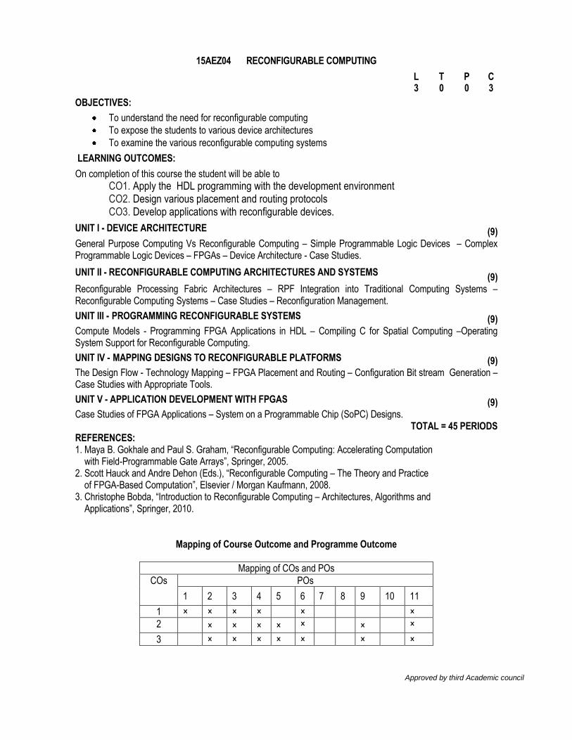
Approved by third Academic council
15AEZ04 RECONFIGURABLE COMPUTING
L T P C 3 0 0 3
OBJECTIVES:
To understand the need for reconfigurable computing
To expose the students to various device architectures
To examine the various reconfigurable computing systems
LEARNING OUTCOMES:
On completion of this course the student will be able to
CO1. Apply the HDL programming with the development environment CO2. Design various placement and routing protocols CO3. Develop applications with reconfigurable devices.
UNIT I - DEVICE ARCHITECTURE (9) General Purpose Computing Vs Reconfigurable Computing – Simple Programmable Logic Devices – Complex Programmable Logic Devices – FPGAs – Device Architecture - Case Studies.
UNIT II - RECONFIGURABLE COMPUTING ARCHITECTURES AND SYSTEMS (9)
Reconfigurable Processing Fabric Architectures – RPF Integration into Traditional Computing Systems – Reconfigurable Computing Systems – Case Studies – Reconfiguration Management.
UNIT III - PROGRAMMING RECONFIGURABLE SYSTEMS (9) Compute Models - Programming FPGA Applications in HDL – Compiling C for Spatial Computing –Operating System Support for Reconfigurable Computing.
UNIT IV - MAPPING DESIGNS TO RECONFIGURABLE PLATFORMS (9) The Design Flow - Technology Mapping – FPGA Placement and Routing – Configuration Bit stream Generation – Case Studies with Appropriate Tools.
UNIT V - APPLICATION DEVELOPMENT WITH FPGAS (9) Case Studies of FPGA Applications – System on a Programmable Chip (SoPC) Designs.
TOTAL = 45 PERIODS REFERENCES: 1. Maya B. Gokhale and Paul S. Graham, “Reconfigurable Computing: Accelerating Computation with Field-Programmable Gate Arrays”, Springer, 2005. 2. Scott Hauck and Andre Dehon (Eds.), “Reconfigurable Computing – The Theory and Practice of FPGA-Based Computation”, Elsevier / Morgan Kaufmann, 2008. 3. Christophe Bobda, “Introduction to Reconfigurable Computing – Architectures, Algorithms and Applications”, Springer, 2010.
Mapping of Course Outcome and Programme Outcome
Mapping of COs and POs
COs POs
1 2 3 4 5 6 7 8 9 10 11
1 × × × × × ×
2 × × × × × × ×
3 × × × × × × ×