nano electronics 2
TRANSCRIPT
8/6/2019 Nano Electronics 2
http://slidepdf.com/reader/full/nano-electronics-2 1/10
NANOTEC HNOLO GIES IN SEMICONDUCTOR ELECTRON ICS
O.P.Pchelyakov, A.I.Toropov, V.P.Popov, A.V.Latyshev, L.V.Litvin, Yu.V.Nastaushev,
D.V.Scheglov and A.L.Aseev
Institute of Semiconductor Physics,
Russian Academy of Sciences, Siberian Branch,
630090 Novosibirsk, pr.acad.Lavrentyeya 13,
Te1:+7(3832)333950, Fax:+7(3832)332771,
E-mail:[email protected]
AbstractThe various technologies for fabrication micro- and nanosized systems included
semicondu ctor, metal and insulator structures are reviewed on the base of the d ata obtainedin Novosibirsk Institute of Semicondu ctor Physics. Main attention is devoted to development
of m ethod of mo lecular beam epitaxy, silicon-on-insulator fabrication process, electron beamlithography and scanning probe nanolithography.
KEYWORDS: semiconductors, micro- and nanostructures, nanotechnology, micro- and
nanoelectronics devices
1. IntroductionRapid progress in semiconductor electronics and transition from microelectronics to
nanoelectronics is followed by development of nanoscale size complementary metal-oxide-
semiconductor transistors (CMOS), single electron tunneling devices, single flux quantum logic,
molecular switching devices, spin devices and wave interference devices. Corresponding progress
of nanotechnologies is important part of this process [11. In present paper the current state of the artand application of technology of molecular beam epitaxy (MBE), direct bonding of semiconductor
wafers, electron beam lithography and probe nanolithography is rewieved on the base of results of
research work carried out at the Novosibirsk Institute of Semiconductor Physics [2]. Among various
diagnostics methods main attention is devoted to the electron microscopy with atomic scale
resolution.
2. Development of Molecular Beam EpitaxyUltra-high vacuum synthesis of thin-layer semiconductor heterocompositions from molecular
and atomic beams is now the main technology of the semiconductor materials science. This
technique presently known as Molecular Beam Epitaxy (MBE) progressed remarkably due to
development of the whole range of micro-, nano-, and optoelectronic devices using
heteroepitaxially grown superlattices, quantum wires and quantum dots which, in contrast to the
previous generations of microelectronic components, directly employ the wave nature of electron.
Semiconductor injection lasers with quantum wells and quantum dots in their active region, high
electron mobility transistors, resonance tunneling diodes and many others nanoengineered
electronic devices would be simply nonexistent without MBE. The birth and rapid progress of
nanotechnology is heavily mediated by molecular beam epitaxy.
Involvement of MBE in the large-scale production of multi-layer epitaxial structures with
atomically smooth interfaces, precisely controlled thickness, composition and impurity doping
9
8/6/2019 Nano Electronics 2
http://slidepdf.com/reader/full/nano-electronics-2 2/10
profile of individual layers demonstrates that this technique in many cases is second to none. High
reproducibility of MBE products is guaranteed by close in situ control of growth processes by
means of very sensitive electron and light beam monitoring techniques as well as a full computer
control of the procedure. It is, however, also known that concerning such important parameters as
wafer throughput and average cost of fabrication the MBE technology is somewhat behind the
chemical vapor deposition (CVD). It is clear that the further progress of UHV technologies is to be
found in combination of the advantages of MBE and CVD through the development of chemical
beam epitaxy
(CBE) or ultra-high vacuum CVD that, in fact, is already done in the field of Ge/Si device oriented
het ero epi ax y.The history of MBE development in the Institute of Semiconductor Physics has been started
by academician A.V.Rzhanov (1920 - 2000), who was the first director of the Institute of
Semiconductor Physics of the Siberian Branch of the Russian Academy of Sciences, and Professor
S.I.Stenin (1940 -1 990), the founder of leading Russian scientific school in physics and technology
of MBE. The first homemade UHV MBE system has been put into operation at Institute in 1979and the high-quality multi-chamber MBE systems has been built in 1992. We have been able to
substantiate the main design principles for MBE growth chambers and to motivate the selection of
an optimal range of analytical instruments for growth control. The full configuration includes the
module for substrate preparation and analysis, the growth chamber for semiconductor epitaxy, and
the module for UHV deposition of metals and insulators. All modules are equipped by a computer-
based system for growth control.
Several pieces of analytical equipment have been developed and are produced at the Institute:
1 Reflection High-Energy Electron Diffraction (RHEED) system for monitoring the surface
structure and crystallinity of grown layers, which is also used for growth rate and epilayer thickness
determination as well as alloy composition measurement.
2.The built-in laser ellipsometer for the measurements of thickness and optical properties of
growing layers on-line. Original techniques and appropriate software makes it possible for the
grower to monitor the film composition, microroughness and surface temperature in situ.
Ellipsometry greatly enhances the possibilities of non-destructive testing and is indispensable in the
cases where M E E D is unsuitable (high pressure in the chamber, low radiation hardness of growing
film).
3 The polarization pyrometer of original design for contactless temperature monitoring during
growth.
Created at the Institute MBE machines “Katun” as well as 32P MBE systems from “Riber”
have been used for growing of the 111-V and Ge/Si epitaxial structures and fabrication the Gunn
diodes for millimeter wavelength range (28 GHz) [3]; GaAs monolithic microwave integrated
circuits [4]; photosensitive GaAs/AlGaAs multiquantum well (MQW) structures [ 5 ] ;
AlGaAs/InGaAs/GaAs high-power microwave field-effect transistors [ 6 ] ; asers with vertical cavity
based on InGaAs quantum well [7]; silicon field-effect transistors with Ge quantum dots in the
ed (3 -5 pm) photodetector arrays on the HgCdTe [9] and GeSi/Si
photosensitive structures the GaAs layer thickness and AlGaAs barriers
I composition have been chosen that the second level in the quantum wells has been lower than the
conduction band edge of AlGaAs to 5-15 meV [5]. The accuracy of manufacture of AlGaAs barrier
composition, interface perfection and uniformity are very important in this case. The high
10
8/6/2019 Nano Electronics 2
http://slidepdf.com/reader/full/nano-electronics-2 3/10
uniformity of the layers thickness has been reached by optimal substrate position angle relatively to
source and the substrate rotation. Moreover, method of growth interruption for surface “flatting”
has been used. The process of “flatting” has been controlled by intensity of W E E D mirror reflex.
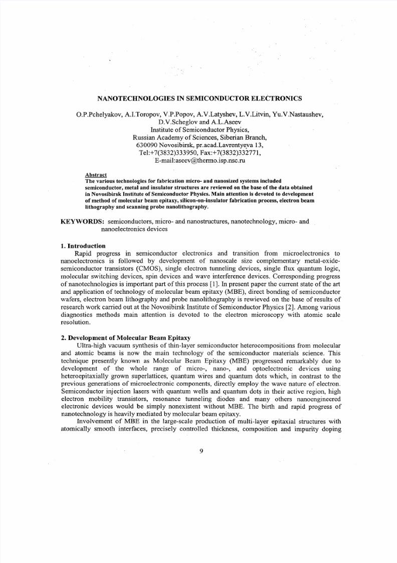
Investigations of MQW structures grown in optimized conditions by means of high resolution
electron microscopy (HREM), low temperature photoluminescence and light Raman scattering have
shown that the interface roughness does not exceed one monolayer (Fig.1).
The photosensitive structure consists 50 periods of GaAs QWs and AlGaAs barriers. On
both sides of photosensitive structures conducting GaAs:Si contacts have been manufactured. The
photodetector array manufactured by the means of photolithography presents liquid etched mesas
40x40 pm periodically located with 50 pm pitch. The ohmic contacts to conducting layers GaAs:Si
have been made by Ge/Au/Ni/Au deposition and annealing. To provide the IR radiance adsorption
in MQW at normal light incidence on the photodetectors array on the substrate side, on each array
element two-dimensional chess-border like diffraction grating has been produced by means of
electron beam lithography and CC12F2 plasma etching. For the hybrid assembling with the silicon
CMOS/CCD multiplexer In bumps of 5-7 pm height have been manufactured. On the base of
MQWs structures the
photosensitive devices for spectral range 7,5-8,8 pm, frame rate 50 Hz, operating temperature 65 Kand photosensitivity 0,06 K have been manufactured [5 ] .
Pseudomorphic AlGaAs/InGaAs/GaAs heterostructures for the microwave transistors have
been grown in a Riber 32P MBE system on semi-insulating GaAs (100) wafers. The sequence of
layers in the structure is given in [6]. The source materials have been ultrapure As with purity of 7N ,gallium with purity of SN, indium with purity of 7N and aluminium with purity of 6N. A residual
gas pressure in MBE chamber has been better as lo-’’ Torr. Detailed investigation of
photoluminescence spectra of intentionally undoped GaAs and AlGaAs layers of different
composition has been carried out in dependence from both exitation power density andmeasurement temperature varied between 4,2 and 30 K. It has been found that free exiton
recombination is dominant channel for recombination of charge carriers in the AlGaAs layers, and
the concentration of nonradiative recombination centers is low. Because background impurities,
oxygen and intrinsic point defects are responsible for nonradiative recombination, a low
concentration of these impurities and defects has been concluded. The low concentration of
background impurities, as carbon and oxygen, is evidently caused by the high degree of segregation
of these impurities at the surface of layers grown under conditions to sustain (3x1) As
supersaturation at growing surface.
These heterostructures have been used to fabricate Schottky-barrier field-effect transistor.
Electron beam lithography has been used to form a gate with length of 0,25 pm and a channel width
up to 300 pm. The transistors has been characterized by increased breakdown voltage up to 25 V
and specific output power of 0,78 W/mm [6].
The technology of MBE has been applied to creation of semiconductor lasers with vertical
cavity provided high external quantum efficiency and high radiation power [7]. The laser structure
contain undoped active region of width h, which include three InGaAs quantum wells of 8 nm thick
mirror regions with p- and n-type doping (Be and Si, respectively), forming Fabry-Perot
interferometer. Interferometer areas consist of multiply repeated GaAs and AlGaAs h/4 layers (20
and 22,5 periods for the p- and n-mirrors, respectively). The GaAs and AlGaAs layers of the
11
8/6/2019 Nano Electronics 2
http://slidepdf.com/reader/full/nano-electronics-2 4/10
mirrors were doped to 10'' cm-3 o ensure carrier injection into active the region through the p- and
n-mirrors. To decrease the ohmic resistance of the mirror regions, the GaAs/AlGaAs interface
contain 15nm thick inserts with an A1 composition gradient and high degree of doping 5x10'' ~ m - ~ .
The top p mirror is terminated with an additional 47 nm thick heavily doped cm-3of Be) GaAs
layer, which functions as the contact region and ensures phase matching of the light reflected from
the Ti/Au metallic coating and the semiconductor heteroboundaries. The aperture of the laser hasbeen determined by the inner diameter of a A1,0, ring, abtained by selective oxidation of the 66 nmthick AlAs layer, located near the active region. The aperture' value has been varied over a range
from 2 to 1000 pm. The radiation of the laser is extracted through a n+ (001) GaAs substrate with an
antireflection coating. The measured reflection spectrum agrees well with the calculated ones and
contains a resonance of the Fabry-Perot interferometer near h=965 nm, whose position is the same
as that of the maximum of the electroluminescence spectrum. The lasing wavelength corresponds
the position of the resonance of the interferometer.
The maximum external differential quantum efficiency of the 60 % has been obtained for an
laser with aperture value of 4 pm. The highest output power up to 10 W at T=300 K and 20 W at
T=250 K in pulsed regime has been obtained for the vertical-cavity laser with aperture value of 500
pm. Thus, the MBE technology has been successklly applied to development of vertical-cavity
semiconductor laser with high extemal quantum efficiency and high radiation power [7].
The long-wavelength infrared photodetector based on MBE grown Ge self-assembled
quantum dots and operating at normal incidence was created recently [ll]. The structure uses
intersubband transitions of holes in the quantum dots. The maximum room temperature peak
detectivity and quantum efficiency of a nonoptimized device structure at about 20 mm were found
to be 1.731 cm
Hz"~/W and 0.1%, respectively. The transitions are found to be redshifted strongly with
increasing voltage so providing an excellent modulator for 10.6 mm CO2 laser radiation. It has beenargued that the observed shift in the intersubband transition energies results from suppression of the
depolarization effect associated with collective response in a dense ensemble of interacting quantum
dots [113.
3. Nanostructures in Si and Ti layers on insulator
The electron beam lithography using focussed electron beam with lateral resolution up to 20 nm[121 has been used to fabricate nano-devices both in thin la ers of Ti and Si on insulating substrates.
Well known PMMA resist layers of molecular weight 10 and 2x10⁶ have been made by powder
dissolution in methylethylketone (25 g/dm3).The resist layers have been spinned on the substrates
at 3000 rpm and the resist thickness has been precisely measured by an ellipsometer. Scanning
electron microscopes equipped by Proxy Writer (Raith) pattem generators have been used for
resists exposure. Wet development of the resists layers has been followed by reactive ion etching
(CC12F2/Ar for Si) and lift-off procedure for Ti.
z
To fabricate Ti nanowire with the lateral tunnel junctions, the ridges on the silicon nitride
thin membranes supported by the silicon substrate have been formed before Ti deposition and
subsequent process of nanowire fabrication (modificated "step edge cut off' - SEC0 technology)
[13]. The Ti nanowires crossed substrate ridge have been 150 nm wide, 2 pm long and 8 nm thick.
To reduce the nanowire contacts to the atmosphere oxygen, the deposition an amorphous Ge layer
12
8/6/2019 Nano Electronics 2
http://slidepdf.com/reader/full/nano-electronics-2 5/10
with a thickness of 8 nm onto the nanowires in the same UHV chamber has been used. Contact pads
and self-aligned gate have been fabricated during lift-off process simultaneously with the Ti wire
formation. The transmission electron microscopy have been used to control topology of the formed
nanostructures.
The both sections of the Ti wire on the side walls of the Si3N4 ridge is much thinner to the
nanowire thickness and due to interaction with residual oxygen transforms to a high-dispersion
system containing TiO, with an effective low potential barrier for electron transport. Measurements
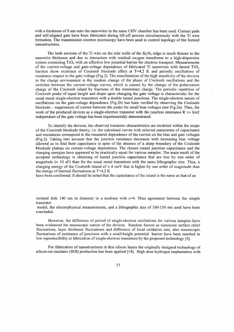
of the current-voltage and gate-voltage dependence of fabricated Ti nanowires with lateral TiO,
barriers show existence of Coulomb blockade effect at T=4,2 K and periodic oscillations of
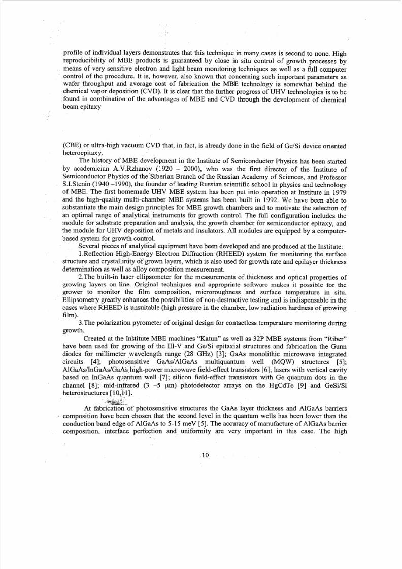
resistance respect to the gate voltage (Fig.2). The manifestation of the high sensitivity of the devices
to the charge environment is the random change of the phase of Coulomb oscillations and the
switches between the current-voltage curves, which is caused by the change of the polarization
charge of the Coulomb island by fractions of the elementary charge. The periodic repetition of
Coulomb peaks of equal height and shape upon changing the gate voltage is characteristic for the
usual metal single-electron transistors with a double tunnel junctions. The single-electron nature of
oscillations on the gate-voltage dependence (Fig.2b) has been verified by observing the Coulomb
blockade - suppression of current between the peaks for small bias voltages (see Fig.2a). Thus, the
work of the produced devices as a single-electron transistor with the junction resistance R >>We2independent of the gate voltage has been experimentally demonstrated.
To identify the devices, the observed transistor characteristics are modeled within the scope
of the Coulomb blockade theory, i.e. the calculated curves with selected parameters of capacitance
and resistances correspond to the measured dependence of the current on the bias and gate voltages
(Fig.2). Taking into account that the junction resistance decreases with increasing bias voltage
allowed us to find their capacitance in spite of the absence of a sharp boundary of the Coulomb
blockade plateau on current-voltage dependence. The chosen tunnel junction capacitance and the
charging energies have appeared to be practically equal for various samples. The main result of the
accepted technology is obtaining of tunnel junction capacitance that are less by one order of
magnitude ( z 10 aF) than for the usual metal transistors with the same lithographic size. Thus, a
charging energy of the Coulomb island of = 4 meV that is higher by one order of magnitude thanthe energy of thermal fluctuations at T=4,2 Khave been confirmed. It should be noted that the capacitance of the island is the same as that of an
isolated disk 140 nm in diameter in a medium with ~=4.hus agreement between the simple
transistor
model, the electrophysical measurements, and a lithographic size of 100-150 nm used have been
concluded.
However, the difference of period of single-electron oscillations for various samples have
been evidenced the mesoscopic nature of the devices. Random factors as nanoscale surface relief
fluctuations, layer thickness fluctuations and difference of local oxidation rate, also mesoscopic
fluctuations of resistance of junctions with a small-height potential barrier have been resulted in
low reproducibility at fabrication of single-electron transistors by the proposed technology [ 6 ] .
For fabrication of nanostructures in thin silicon layers the originally designed technology of
silicon-on-insulator (SOI) production has been applied [141. High dose hydrogen implantation with
13
8/6/2019 Nano Electronics 2
http://slidepdf.com/reader/full/nano-electronics-2 6/10
subsequent annealing has been used to delaminate a thin layer of silicon from a thick substrate
bonded with an oxidized silicon wafer. High quality buried oxide layer, top silicon layer and high
perfection of the interface between layers are the main advantages of this technology. The thickness
of the initial silicon top layer is managed by energy of implanted hydrogen ions and can be in the
range of 200-2000 nm. The further reduction of SO 1 layer thickness has been achieved by dry
oxidation of the wafers followed by stripping in diluted HF. The thickness and uniformity of the
remaining SO1 layer and interface have been determined by spectroscopic ellipsometry
measurements. This technological process provides the thickness of SO1 about of 3 nm with
thickness nonuniformity of 1 nm for 4 inch wafer. Both the transmission electron microscopy and
high resolution electron microscopy investigations revealed the high perfection of the produced
silicon layers and silicon-insulator interfaces [141. Top silicon layers have been additionally doped
with boron or phosphorous ions with following activation of dopant at 1100 C for 2 h. As a result,
nanostructures with different doping levels have been created.
The nanostructures of various topology have been formed by using an electron beam
lithography, a chemical wet development of PMMA, plasma chemical dry etching of silicon top
layer and metal contacts by lift-off technique. Ultra high vacuum field emission scanning electron
microscope from ‘Tesla’ without beam blanking has been used for resist layer exposure with the
dwell time about 7 mks. Typical parameters of electron beam source are 22 keV, 1nA.
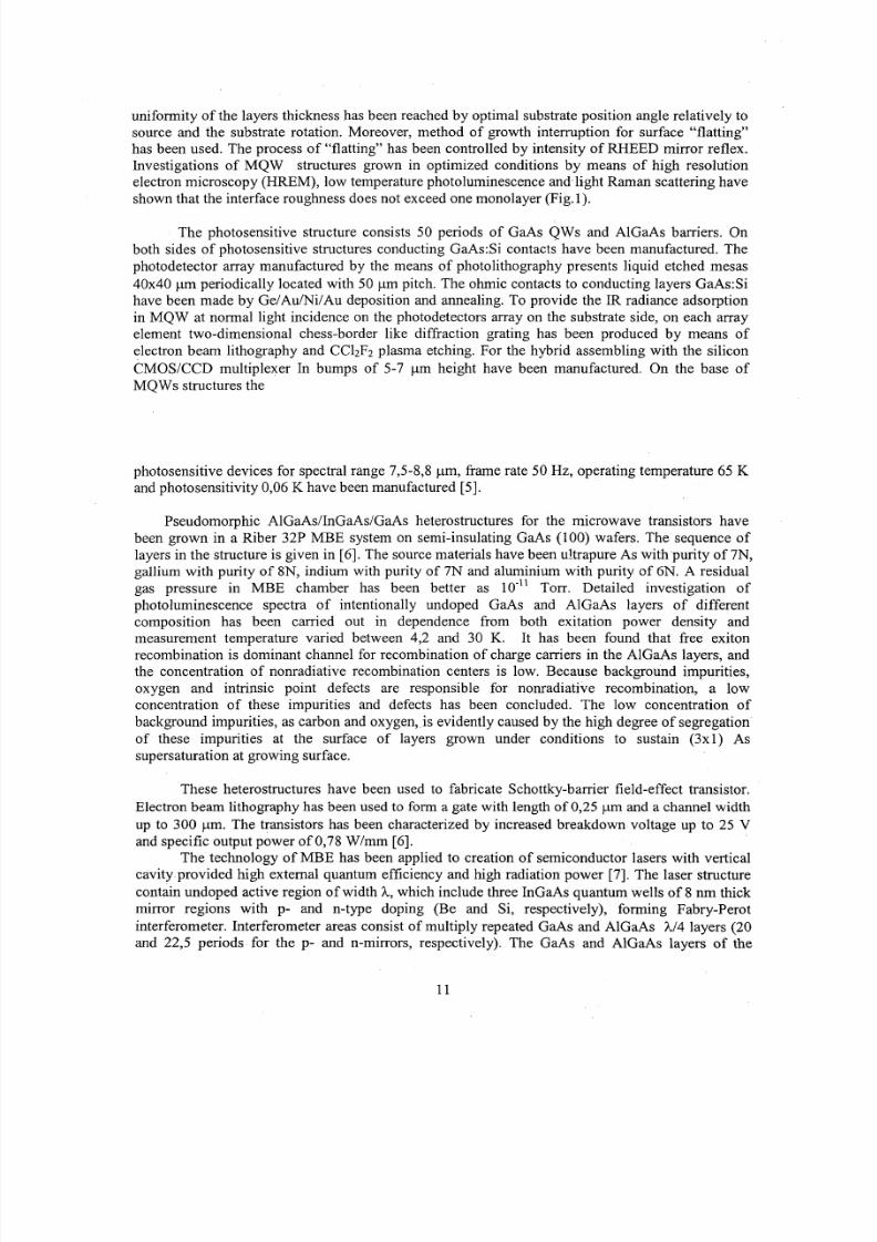
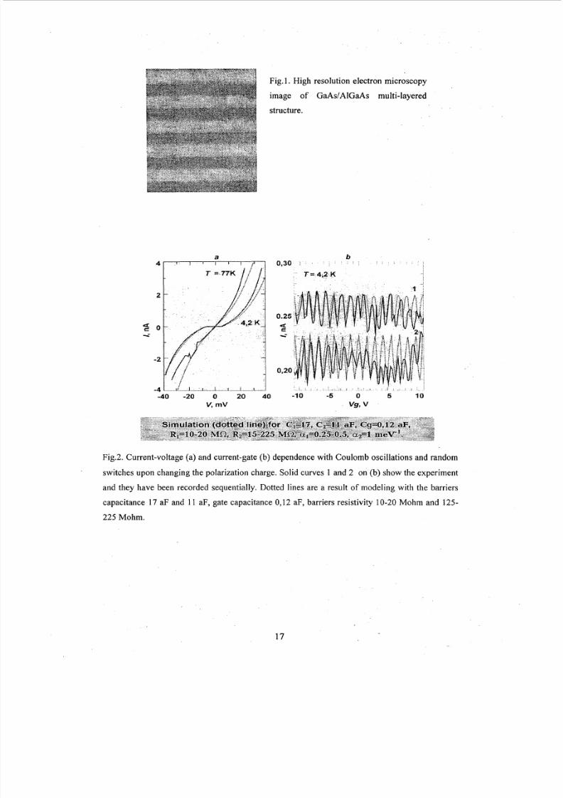
Fig.3 a represent scanning electron microscopy image of multichannel “fin”-gate SO1
transistor formed by etching of initially uniform silicon layer (dark lines). Areas of silicon layer top
and low are source and drain, respectively, connected by multichannel created by electron beam
lithography. Gate of 0,25 pm width is located diagonally and cover each silicon channel with
formation of “fin”-like configuration. In this case SO1layer has been 44 nm thick. The drain-source
resistance at room temperature has been practically independent on drain and gate voltage following
electron gas degeneration. The results of the measurements of the current-voltage characteristics are
presented in Fig.3b. A pronounced current-gate characteristics are observed in dependence from
source-drain voltage as well as from substrate voltage. The modulation of the drain-source current
by the gates voltage has been detected at room temperature measurements of fabricated SO1
nanostructures and in dependence from substrate voltage the various conductivity of channels has
been realized. The results obtained indicate a perspective for using SO1 structures for creation new
generation of silicon nanodevices.
4. Scanning probe nanolithographyFurther development of nanopatterning technology methods is concerned with using of
scanning probe microscopy (SPM) and scanning probe nanolithography. A scanning probe
nanolithography is highly promising tool for achieving notable size reduction and accordingly for
fabricating nanometer scale objects (see for example [15]). In order to modify surfaces SPM have
been used in a wide variety of operational modes (for a review see [16]) but one of the most
common techniques, however, is local oxidation of substrates by applying electric signals to the
SPM tip.
Investigation of tip-induced local anodic oxidation of the titanium, gallium arsenic and
silicon films has been done recently [17]. The number of parameters such as applied voltage,
oxidation time, host material and relative humidity has been under consideration. The special
attention was given to investigation of peculiarities of extra thin film local anodic oxidation. To
14
8/6/2019 Nano Electronics 2
http://slidepdf.com/reader/full/nano-electronics-2 7/10
reduce the roughness of studied surfaces, the large step-free areas on vicinal silicon surfaces were
prepared in an UHV chamber of electron microscope by using electromigration phenomena [181.
An atomic force microscope (Solver P-47H, NT-MDT) has been performed to carry out
experiments at ambient conditions. The sample was cut from a silicon wafer with misorientation
angle less than 1 from the (1 11) plane. A clean silicon surface was prepared by high temperature
annealing in an ultrahigh vacuum chamber of reflection electron microscope (REM). Cleaning
process was controlled by an image mode of reflection electron microscopy. Direct REM
observation allows to control roughness of the silicon surface. The sample has been heated by
passing a direct electric current. Using phenomenon of monatomic step rearrangement, induced by
electromigration effect of silicon-adatoms, large flat terraces have been fabricated on the silicon
(1 11) surface. The average distance between monoatomic steps (terrace width) is as 3-4 pm.
The sample holder has a contact pad to connect the sample to electric wires of microscope.
Titanium film with 40 Angstrom thickness on the silicon (1 11) surface with natural oxide was
deposited from an electron gun evaporate in an UHV chamber at room temperature. AFM images
were obtained in the resonant mode with platinum coated silicon cantilevers (v=150 kHz).
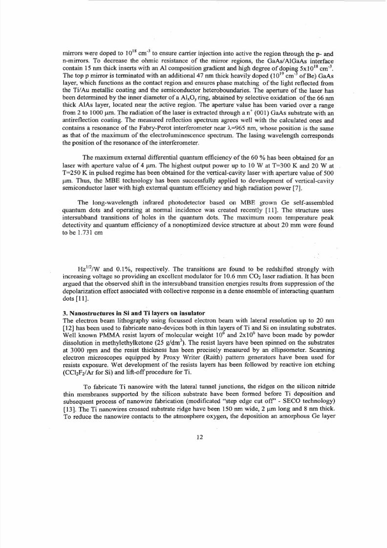
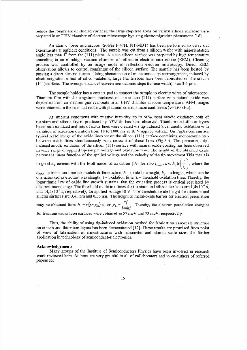
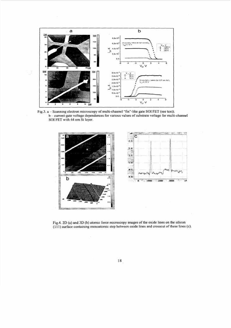
At ambient conditions with relative humidity up to 50% local anodic oxidation both oftitanium and silicon layers produced by AFM-tip has been observed. Titanium and silicon layers
have been oxidized and sets of oxide lines were created via tip-induced local anodic oxidation with
variation of oxidation duration from 10 to 1000 ms at 10 V applied voltage. On Fig.8a one can see
typical AFM image of the oxide lines set on the silicon (111) surface containing monoatomic step
between oxide lines simultaneously with crosscut of these lines (Fig.8b). The permanent tip-
induced anodic oxidation of the silicon (1 11) surface with natural oxide coating has been observed
in wide range of applied tip-sample voltage and oxidation time. The height of the obtained oxide
patterns is linear function of the applied voltage and the velocity of the tip movement This result is
in good agreement with the Mott model of oxidation [19] for t >> t,,, :h oc h, In - , where the( t1ttrnns--a transition time for models differentiation, h - oxide line height, h, - a length, which can be
characterized as electron wavelength, t - oxidation time, t c - threshold oxidation time. Thereby, thelogarithmic law of oxide line growth sustains, that the oxidation process is critical regulated by
electron interchange. The threshold oxidation times for titanium and silicon surfaces are 1,4x10⁻⁴s,
and 14 ,5 ~1 0- ~, respectively, for applied voltage 10V. The threshold oxide height for titanium and
silicon surfaces are 0,41 nm and 0,36 nm . The height of metal-oxide barrier for electron percolation
1may be obtained from h, = q(8mjyo)-T, or j y o =-. Thereby, the electron percolation energies
8mh:
for titanium and silicon surfaces were obtained as 57 meV and 73 meV, respectively.
Thus, the ability of using tip-induced oxidation method for fabrication nanoscale structure
on silicon and thitanium layers has been demonstrated [17]. These results are promised from point
of view of fabrication of nanostructures with nanometer and atomic scale sizes for further
application in technology of semiconductor electronics.
AcknowledgementsMany groups of the Institute of Semiconductors Physics have been involved in research
work reviewed here. Authors are very grateful to all of collaborators and to co-authors of referred
papers for
15
8/6/2019 Nano Electronics 2
http://slidepdf.com/reader/full/nano-electronics-2 8/10
valuable contribution. This work has been supported by the Programs of Russian Ministery of
Industry, Science and Technologies as well as by grants of Russian Found of Basic Researches.
References
1.
2.
3.
4.
5.
6.
7.
8.
9.
Technology Roadmap for Nanoelectronics, Ed.R.Compano, European Comission, , Brussels,
2000, 104 p.
O.P.Pchelyakov, A.I.Toropov, V.P.Popov, A.V.Latyshev, L.V.Litvin, Yu.V.Nastaushev and
A.L.Aseev, Proc.SPIE, 2002, v.4900, p.247-256.
A.I.Kurkan, T.A.Bannova, O.B.Koretskaya, L.P.Porokhovnichenko, 0.P.Pchelyakov a.o.,
Electronic Industry, 1999, No.1-2, p.95-97 (in Russian).
V.V.Chaldyshev, M.A.Putyato, B.P.Semyagin, V.V.Preobrazhenskii, 0.P.Pchelyakov a.o.,
Electronic Industry, 1999, No.1-2, p.154-158 (in Russian).
V.N.Ovsyuk, Yu.G.Sidorov, V.V.Vasilyev, V.V.Shashkin, Applied Physics, 2000, No.5, p.70-
79 (in Russian).
K.S Zhuravlev, A.I.Toropov, T.S.Shamirzaev, A.K.Bakarov, Yu.N.Rakov, Yu.B.Myakishev,
Tech.Phys.Lett., 1999, v.25, No.8, p.595-597.
V.A.Gaisler, A.I.Toropov, AKBakarov, AKKalagin, N.T.Moshegov, D.A.Tenne,
M.M.Kachanova, O.R.Kopp, L.A.Henasheva, A.S .Medvedev, Tech.Phys.Lett., 1999, v.25,
A.I.Yakimov, C.J.Adkins, R.Boucher, A.V.Dvurechensky, 0.P.Pchelyakov a.o., Phys.Rev.B,
1999, v.59, p.12598.
Yu.G.Sidorov, S.A.Dvoretsky, M.V.Yakushev a.o., Thin Solid Films, 1997, v.306, p.253.
N0.10, p.775-777.
10. A.I. Yakimov, A.V. Dvurechenskii, A.I. Nikiforov, O.P. Pchelyakov, A.A. Nenashev, Phys.
11. A. I. Yakimov, A. V. Dvurechenskii, A. I. Nikiforov, and Yu. Yu. Proskuryakov, J. of Appl.
12. Y.V.Nastaushev, T.Gavrilova, M.Kachanova, V.Kolosanov, O.V.Naumova, V.P.Popov,
A.L.Aseev, Materials Science and Engineering C, 2002, v. 19, p. 189-192.
13. D.G.Baksheev, V.A.Tkachenko, L.V.Litvin, V.A.Kolosanov, K.P.Mogilnikov, A.G.Cherkov,
A.L.Aseev, Optoelectronics, Instrumentation and Data Processing, Allerton Press, Inc.,New
York, 2001, No.3, p.99-113.
14. V.P.Popov, I.V.Antonova, V.F.Stas, L.V.Mironova, A.K.Gutakovskii, E.V.Spesivtsev,
A.S.Mardezhov, A.A.Franzusov, G.N.Feofanov, Materials Science and Engineering B, 2000,
v.73, p.82.
15. D.Sarid, in: Scanning Force Microscopy, Oxford Series in Optical and Imaging Sciences,
Oxford University Press, Oxford, 1994.
16. C.R.K.Marrian (Ed.), Technology of Proximal Probe Lithography, SPIE Optical Engineering
Press, Bellingham, WA, 1993.
17. D.V.Sheglov, A.V.Prozorov, D.A.Nasimov, A.V.Latyshev and A.L.Aseev, In: Scanning Probe
Microscopy, 2002, Institute for Physics of Microstructures, N.Novgorod, p. 126-128.
18. A.V.Latyshev, A.L.Aseev, A.B.Krasilnikov and S.I.Stenin., Surface Science, 1989, v.213, p.157.
19. N.F. Mott, Trans. Faraday Soc., 1939, v.35, p.1175; Trans. Faraday Soc., 1940, v.36, p.472.
Rev. B, 2000, v.62, No.24; p. .Phys., 2001, ~ .89 ,N0.10, .5676-5681.
16
8/6/2019 Nano Electronics 2
http://slidepdf.com/reader/full/nano-electronics-2 9/10
Fig. 1. High resolution electron microsco py
image of GaAdAIGaAs multi-layered
structure.
a b4 ' 1 ' 1 ' 1 : ' 0,30
T =77K 1: /] T = 4,2 K -
2
0.25
PO 3-4- 2-
-2
0,20
Simulation (dotted linej f o r C1=l?,C p l l aF,Cg=0,12 aF,
R1=10-20 MR , R2=15-225 MQ,' t~l=0.25-0 .5,C Z Z = ~ I 1 1 e V ' .
Fig.2. Current-voltage (a) and current-gate (b) d ependence with C oulomb oscillations and random
switches upon chang ing the polarization charge. Solid curves 1 and 2 on (b) show the experiment
and they h ave been recorded sequentially. Dotted lines are a result of modeling with the barriers
capacitance 17 aF and 1 1 aF, gate capacitance 0,12 aF, barriers resistivity 10-20 Mohm and 125-
225 Mohm.
17
8/6/2019 Nano Electronics 2
http://slidepdf.com/reader/full/nano-electronics-2 10/10
a
Fig.3. a - Scanning electron microscop y of m ulti-channel “fin”-like gate SO1 FE T (see text).b - urrent-gate voltage dependen ces for various values of substrate voltage for mu lti-channel
SO1 FET w ith 44 nm Si layer.
Fig.4.2 D (a) and 3D (b) atomic force microscopy image s of the oxide lines on the silicon(111) surface containing monoatom ic step between oxide lines and crosscut of these lines (c).
18