nano-scale convective heat transfer of vertically … convective heat transfer of vertically aligned...
TRANSCRIPT

Nano-Scale Convective Heat Transfer of Vertically Aligned Carbon Nanotube Arrays
A Major Qualifying Project Report
Submitted to the Faculty of the
WORCESTER POLYTECHNIC INSTITUTE
in partial fulfillment of the requirements for the
Degree of Bachelor of Science
in Mechanical Engineering
by
Alex Larsen
Ryan Whetstone
Date: 2010
_______________________________________
Approved:
Prof. Jianyu Liang, Major Advisor
Project Number: MQP-JNL-CNT9
1
Abstract .................................................................................................................................................. 3
Introduction ............................................................................................................................................ 3
Background ............................................................................................................................................. 4
Basics of CNTs...................................................................................................................................... 4
CNT Production Methods..................................................................................................................... 6
Arc-Discharge .................................................................................................................................. 6
Laser Ablation .................................................................................................................................. 7
Chemical Vapor Deposition (CVD) .................................................................................................... 8
Material Properties of CNTs ............................................................................................................... 10
Applications of CNTs .......................................................................................................................... 11
Heat Sink Design: Present and Future ................................................................................................ 12
Heat Sink Design Overview ............................................................................................................ 12
Micro Heat Sink Design Strategies .................................................................................................. 14
Potential for Aligned MWCNT Heat Sink ............................................................................................ 15
Design and Construction .................................................................................................................... 16
Anodized Aluminum Oxide (AAO) Template Anodization: .............................................................. 17
Template Assisted MWCNT Growth: .............................................................................................. 18
Thermocleaning ............................................................................................................................. 19
Etching .......................................................................................................................................... 20
Imaging and Testing Methods ............................................................................................................ 21
Scanning Electron Microscope Imaging .......................................................................................... 21
Comparative Testing Method ............................................................................................................ 23
Methodology ......................................................................................................................................... 24
Sample Preparation ........................................................................................................................... 24
CNT Growth ................................................................................................................................... 24
Thermocleaning Optimization ........................................................................................................ 26
Etching Optimization ..................................................................................................................... 28
Comparative Testing .......................................................................................................................... 29
Testing Setup ................................................................................................................................. 29
Virtual Instrumentation ................................................................................................................. 32
Thermal Testing Technique ............................................................................................................ 36
Temperature Calibration ................................................................................................................ 36

2
Results and Analysis .............................................................................................................................. 38
Conclusions ........................................................................................................................................... 43
Acknowledgments
We would like to thank all the members of the WPI Nanomaterials & Nanomanufacturing
Laboratory (NNL) for all of their help and input with our project:
Nihar Pradhan
Qiming Yang
Yuqin Yao
Siddharth Meshram
Sara Gouveia
And our advisor Prof. Jianyu Liang
3
Abstract
The trend of miniaturization in electronics has led to much greater heat densities within
computer chips, demanding high performance heat sinks at smaller and smaller scales. A
vertically aligned array of carbon nanotubes could function analogously to a conventional fin or
pillar heat sink. Using a nano-porous aluminum oxide template, aligned CNTs were grown by
chemical vapor deposition, and processing parameters were varied for comparison. By applying
a constant heat input, the steady state temperature was measured for different surface
morphologies, enabling insight into nano-scale convection properties.
Introduction
Scientific investigation allows us to imagine, explore, and understand new realms of
knowledge and possibilities for application. With the advancements in computer processing,
microscopy, and micro-scale manufacturing, a previously inaccessible niche in science has
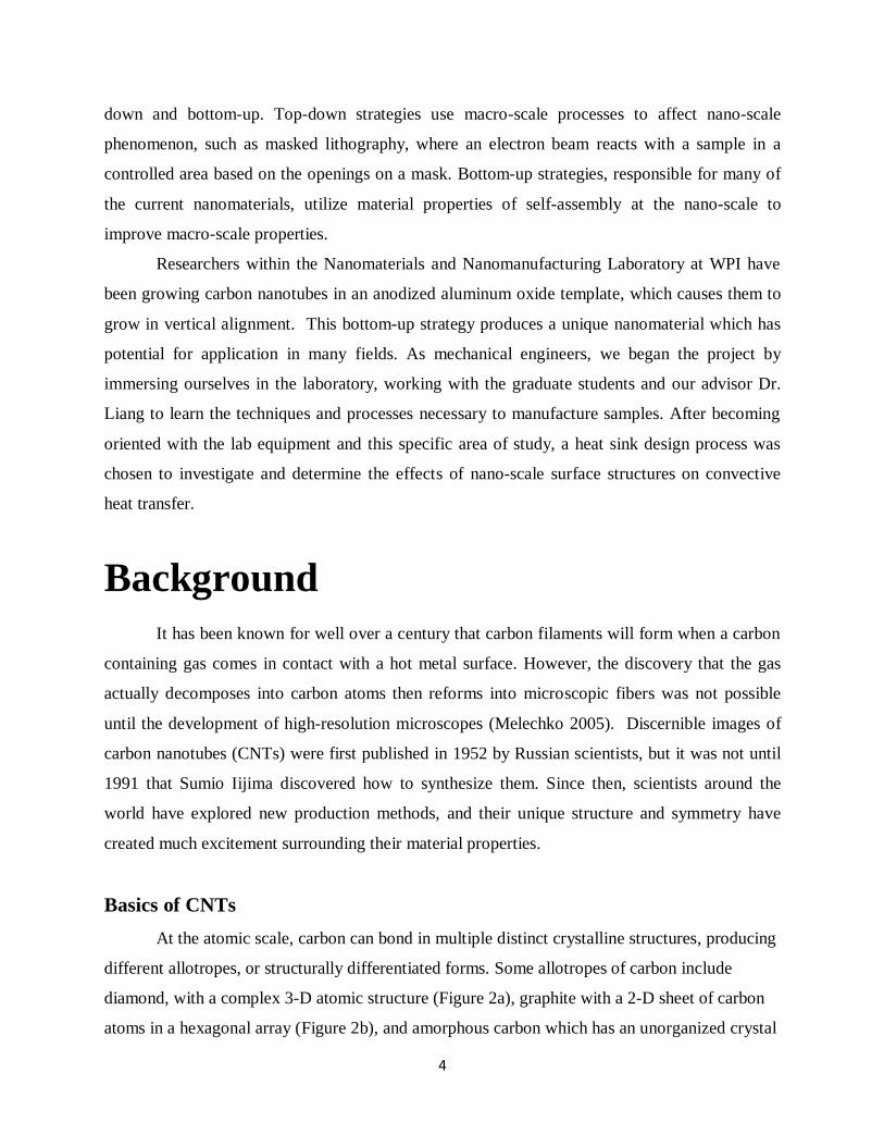
opened at the most minuscule end of the size spectrum, known as nanotechnology. The “nano”
in nanotechnology refers to the scale of a nanometer (nm), one billionth of a meter, but
realistically, nanotechnology involves the
development of materials and devices with
distinct properties up to the hundred nanometer
range. Figure 1 compares the scale of a multi-
walled carbon nanotube (MWCNT) with other
microscopic objects.
Since the early 1990s, there has been a
worldwide buzz surrounding nanotechnology,
resulting in huge advances in its science and
applications. Possibilities for manipulation of
objects and creation of devices at the nano scale
can be broken down into two categories, top-Figure 1: MWCNT scale compared to microscopic objects
4
down and bottom-up. Top-down strategies use macro-scale processes to affect nano-scale
phenomenon, such as masked lithography, where an electron beam reacts with a sample in a
controlled area based on the openings on a mask. Bottom-up strategies, responsible for many of
the current nanomaterials, utilize material properties of self-assembly at the nano-scale to
improve macro-scale properties.
Researchers within the Nanomaterials and Nanomanufacturing Laboratory at WPI have
been growing carbon nanotubes in an anodized aluminum oxide template, which causes them to
grow in vertical alignment. This bottom-up strategy produces a unique nanomaterial which has
potential for application in many fields. As mechanical engineers, we began the project by
immersing ourselves in the laboratory, working with the graduate students and our advisor Dr.
Liang to learn the techniques and processes necessary to manufacture samples. After becoming
oriented with the lab equipment and this specific area of study, a heat sink design process was
chosen to investigate and determine the effects of nano-scale surface structures on convective
heat transfer.
Background
It has been known for well over a century that carbon filaments will form when a carbon
containing gas comes in contact with a hot metal surface. However, the discovery that the gas
actually decomposes into carbon atoms then reforms into microscopic fibers was not possible
until the development of high-resolution microscopes (Melechko 2005). Discernible images of
carbon nanotubes (CNTs) were first published in 1952 by Russian scientists, but it was not until
1991 that Sumio Iijima discovered how to synthesize them. Since then, scientists around the
world have explored new production methods, and their unique structure and symmetry have
created much excitement surrounding their material properties.
Basics of CNTs
At the atomic scale, carbon can bond in multiple distinct crystalline structures, producing
different allotropes, or structurally differentiated forms. Some allotropes of carbon include
diamond, with a complex 3-D atomic structure (Figure 2a), graphite with a 2-D sheet of carbon
atoms in a hexagonal array (Figure 2b), and amorphous carbon which has an unorganized crystal

5
structure (Thostenson 2001).
Figure 2: (a) diamond atomic structure (b) graphite atomic structure (EveryScience 2009)
Cylindrical allotropes of carbon can also form,
where the atoms are bonded as if a graphite sheet,
composed of hexagonal cells, were rolled into a tube. The
bonding morphology of a CNT can have three known
forms, armchair, zigzag, and chiral, based on the
orientation of the horizontal cells (Figure 3).
CNTs can be divided into two main categories depending on the number of graphite
layers in the tube. The smallest CNTs exist as one carbon layer cylinders, known as single-
walled carbon nanotubes (SWCNTs), with very small diameters ranging from about 1-5 nm.
There can also be CNTs nested within other CNTs, known as multi-walled carbon nanotubes
(MWCNTs) with diameters up to 250 nm. The many concentric rings of CNTs closely spaced
within a MWCNT are held together with relatively weak Van der Waals forces (Thostenson
2001). CNTs can be grown using multiple production methods, which has resulted in a plethora
of CNT structures.
Figure 3: Three possible carbon nanotube atomic structures

6
CNT Production Methods
Since the early 1990s, when Iijima first synthesized CNTs, three primary production
methods have been developed: arc-discharge, laser ablation, and chemical vapor deposition.
Based on the production method and the specific growth parameters, many different types of
micro and nano scale carbon fibers have been produced, each with different structures and
properties.
Arc-Discharge
The arc-discharge method is the original synthesis technique used by Iijima, and has
proven to be the simplest process to date. The main components of this technique are two high-
purity graphite rods, which act as an anode and a cathode. Under an inert atmosphere of helium,
a voltage is applied between the rods until a stable arc is achieved. This electrical arc strips
carbon atoms off the anode and deposits them on the cathode forming a build-up consisting of a
hard carbon shell with a soft core containing CNTs and other carbon particles (Thostenson
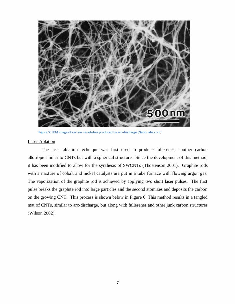
2001). This process is shown below in Figure 4, and the resulting CNTs are shown in Figure 5.
Figure 4: Schematic of arc-discharge process
7
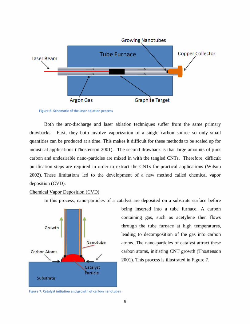
Laser Ablation
The laser ablation technique was first used to produce fullerenes, another carbon
allotrope similar to CNTs but with a spherical structure. Since the development of this method,
it has been modified to allow for the synthesis of SWCNTs (Thostenson 2001). Graphite rods
with a mixture of cobalt and nickel catalysts are put in a tube furnace with flowing argon gas.
The vaporization of the graphite rod is achieved by applying two short laser pulses. The first
pulse breaks the graphite rod into large particles and the second atomizes and deposits the carbon
on the growing CNT. This process is shown below in Figure 6. This method results in a tangled
mat of CNTs, similar to arc-discharge, but along with fullerenes and other junk carbon structures
(Wilson 2002).
Figure 5: SEM image of carbon nanotubes produced by arc-discharge (Nano-labs.com)
8
Both the arc-discharge and laser ablation techniques suffer from the same primary
drawbacks. First, they both involve vaporization of a single carbon source so only small
quantities can be produced at a time. This makes it difficult for these methods to be scaled up for
industrial applications (Thostenson 2001). The second drawback is that large amounts of junk
carbon and undesirable nano-particles are mixed in with the tangled CNTs. Therefore, difficult
purification steps are required in order to extract the CNTs for practical applications (Wilson
2002). These limitations led to the development of a new method called chemical vapor
deposition (CVD).
Chemical Vapor Deposition (CVD)
In this process, nano-particles of a catalyst are deposited on a substrate surface before
being inserted into a tube furnace. A carbon
containing gas, such as acetylene then flows
through the tube furnace at high temperatures,
leading to decomposition of the gas into carbon
atoms. The nano-particles of catalyst attract these
carbon atoms, initiating CNT growth (Thostenson
2001). This process is illustrated in Figure 7.
Figure 6: Schematic of the laser ablation process
Figure 7: Catalyst initiation and growth of carbon nanotubes

9
By using lithography techniques, a mask can be produced which allows for controlled
size and spacing of the catalyst deposition. Although limited alignment has been observed due to
van der Waal interactions between neighboring CNTs, the result of basic CVD is still generally a
tangled mat of CNTs (Melechko 2005). It was not until the development of plasma enhanced
chemical vapor deposition (PECVD) that true vertical alignment of CNTs was achieved.
PECVD is similar to CVD since the deposition of a nano-particle of catalyst is required
to begin CNT growth. The primary difference between these methods is that during CVD,
vaporization of the carbon gas occurs via thermal energy only, while in PECVD a voltage is
applied during the growth process. This causes current flow through a plasma medium within the
furnace tube, bombarding the carbon gas
electrons. This electrical energy input
reduces the activation energy for CNT
growth, and therefore decreases the
process temperature required for the
reaction. The most important, albeit
unexpected benefit of PECVD is the
vertical alignment caused by interactions
with the electric field. This field causes
each CNT to grow almost completely
vertical, minimizing entanglement with
its neighbors as seen in Figure 8 (Melechko 2005).
Another CVD method which results in vertically aligned CNTs uses a specialized
material with closely packed nano-diameter pores as a template. Materials such as anodized
aluminum oxide (AAO) have a high density of vertical nanopores, which extend completely
through the ceramic matrix. Through CVD, carbon atoms can be deposited on the inside walls of
these nanopores to form MWCNTs, in some cases even without a catalyst. The resulting CNTs
are many layers thick and are vertical since they follow the direction of the pores. This vertical
alignment is desirable for many applications.
These three basic categories of production have diversified into hundreds of specific,
highly deterministic modes of CNT synthesis, which means the position, alignment, diameter,
Figure 8: Vertically aligned carbon nanotubes after plasma enhanced chemical vapor deposition (Shaikh 2007)

10
length, and chemical composition of individual nanostructures can be manipulated (Melechko
2005). This evolution has enabled production of CNTs with unprecedented material properties.
Material Properties of CNTs
CNTs have been shown to have incredible mechanical, electrical, and thermal properties,
some of which have been reported to exceed any other known material. Despite the amazing
properties of CNTs already witnessed, very few have reached the theoretical predictions
calculated for idealized CNT structures. This means more work is required in optimizing
production methods, in order to limit the defects and resistances which lead to the less than
anticipated results (Thostenson 2001).
Scientific interest in CNTs was first sparked by the discovery that they possess
remarkable mechanical properties. In macro-scale structural materials, there is always a trade-off
between strength and ductility, with strong materials tending to be brittle, and ductile materials
tending to be weak. CNTs have been shown to have remarkably high strength, stiffness, fracture
resistance, and elastic modulus, while still maintaining significant flexibility and ductility in the
sense that they can withstand high longitudinal strain and bending moments. In the axial
direction, MWCNTs are one of the strongest and stiffest known materials, with a measured
tensile strength and elastic modulus of 150 GPa and 900 GPa, respectively, versus about 0.65 - 3
GPa and 200 GPa for stainless steel (Demczyk 2002). In other words, CNTs are over 100 times
stronger than steel at only a minuscule fraction of its weight. In contrast to CNTs high tensile
strength, they tend to buckle easily under compression as a result of their large aspect ratio.
CNTs are also attributed with having excellent thermal and electrical conductivity in the
axial direction. Due to the unique structure of CNTs with the „armchair‟ morphology, superb
electrical properties are believed to exist. Theoretical calculations of electrical current density
range from 109 to 10
13 A/cm
2, and experimentally a SWCNT has been measured to be 10
7 A/cm
2,
about 100 times greater than copper (Hong 2007). All CNTs are expected to be very good
thermal conductors exhibiting a property called ballistic conduction, defined as the unimpeded
flow of heat phonons through a material.
For a single discreet MWCNT, thermal conduction has already been measured to be
about 3000 W/mK, only half its theoretical prediction (Kim 2001). Experimental testing of
CNTs has resulted in a wide range of measurements which rarely correlate with their theoretical
11
estimation. There are many possible explanations for this observed range, such as defects from
the manufacturing process, and non-comparable testing procedures. For instance many testing
methods use „mats‟ of aligned CNTs, and interpolate their results for a single tube. This method
has proven to be inaccurate since large resistances exist between neighboring tubes. Recent
experiments using isolated CNTs have resulted in more accurate measurements, but additional
research is still required.
Applications of CNTs
The size and properties of CNTs have resulted in thousands of proposed applications
which could revolutionize a wide range of fields. Already, some incredible applications have
been realized by utilizing their unique mechanical, electrical and thermal properties.
CNTs‟ high tensile strength and stiffness allows for many potential applications. If CNTs
are woven into a fabric they can be used as stab proof and bullet proof combat jackets. The high
tensile strength may eventually allow CNTs to replace steel in many applications such as the
cables on suspension bridges and the reinforcement bars in concrete. If tensile strength can be
increased further, it may allow for the development of a space elevator. This project proposes to
create a tether between the earth and a space station which can transport supplies and personnel
(LiftPort 2009).
The unique network of carbon-carbon bonds which make up the CNTs leads to excellent
electrical properties which may one day lay the groundwork for micro and nano-scale electronic
devices. One of the most promising electrical applications are tiny interconnects between
miniature electronic devices. The high thermal stability and most importantly the extremely
large current carrying capacity, allow for performance comparable and even surpassing current
macro-scale copper interconnects (Naeemi 2007). Mixing CNTs into various matrixes creates
advanced composites which can have enhanced or additional properties. For example plastics
are typically electrical insulators, but when a small amount of CNTs are evenly dispersed they
can become conductors (Jimenez 2007).
CNTs also present potential for thermal applications, since they are one of the only
known materials which exhibit a phenomenon known as ballistic conduction, where units of heat
called phonons travel through the structure virtually unimpeded. One idea is that CNTs could
someday be used to destroy cancer cells by thermally activating them within a tumor using radio

12
waves. While this type of application is still years from being realized, the thermal properties of
CNTs can be useful for the performance enhancement and miniaturization of heat sinks, which
act to dissipate heat as quickly as possible from a thermal system.
Heat Sink Design: Present and Future
Modern heat sinks usually consist of an array of thermally conductive metal pillars or fins
which are connected to a heat source. To remove heat, a fluid is directed through a heat sink
structure and heat dissipates as it flows over the surface. This form of heat transfer between a
solid surface and a surrounding fluid is called convection. Maximizing the convective heat
transfer between a heat sink and the fluid is critical and will be a key challenge in the
miniaturization of electronics.
Heat Sink Design Overview
A heat sink‟s effectiveness depends on the thermal interface between the heat source and
the heat sink, the thermal properties of the material used, and the shape of the heat sink. A
general heat sink schematic is shown below in Figure 9.
The connection between a heat source
and the bottom of a heat sink is known as a
thermal interface. Good thermal conductivity is
needed at the thermal interface for heat to flow
efficiently from the heat source to the heat
sink. Maximized physical contact between the
surfaces is also critical, but even the flattest
surfaces encountered only make true molecular
contact at 1-2% of the surface area (Garimella
2006). This issue is addressed by using a
thermal interface material (TIM) to mate the
two surfaces on the molecular level. Silicon-based thermal grease and powdered silver paste are
two commonly used TIMs, with thermal conductivities of 1-3 and 8 W/mK, respectively. These
thermally conductive, viscous, liquids displace the thermally non-conductive air (0.024 W/mK)
which would normally occupy the empty spaces between the surfaces (Conway 2006).
Figure 9: Basic heat sink design
13
Optimized thermal interfaces with minimum thermal resistance are necessary for maximized heat
sink performance.
Once heat has crossed the thermal interface, the heat sink material should be able to
transport heat away from the source as quickly as possible. The free electrons in many metals
give them very high thermal conductivity. Aluminum (≈ 250 W/mK) and copper (≈ 400 W/mK)
are the most commonly used materials for heat sink structures. Due to fast heat flow, low
material cost, and relatively easy processing, these two metals are ideal for commercial use in
today‟s computers. However, as electronics become more miniaturized, new materials and
methods will be required to dissipate heat at much smaller scales.
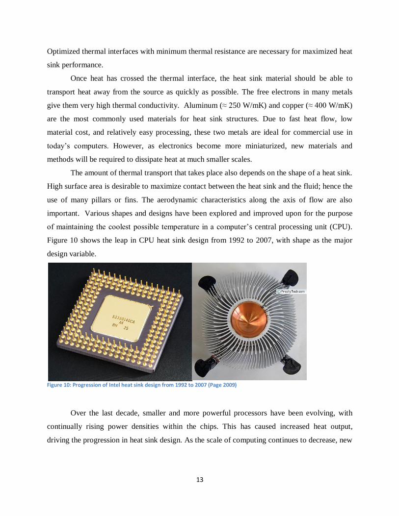
The amount of thermal transport that takes place also depends on the shape of a heat sink.
High surface area is desirable to maximize contact between the heat sink and the fluid; hence the
use of many pillars or fins. The aerodynamic characteristics along the axis of flow are also
important. Various shapes and designs have been explored and improved upon for the purpose
of maintaining the coolest possible temperature in a computer‟s central processing unit (CPU).
Figure 10 shows the leap in CPU heat sink design from 1992 to 2007, with shape as the major
design variable.
Figure 10: Progression of Intel heat sink design from 1992 to 2007 (Page 2009)
Over the last decade, smaller and more powerful processors have been evolving, with
continually rising power densities within the chips. This has caused increased heat output,
driving the progression in heat sink design. As the scale of computing continues to decrease, new

14
designs are beginning to explore micro and nano scale heat sink applications. Noteworthy
engineering strategies for micro heat sink design are discussed in the next section.
Micro Heat Sink Design Strategies
When designing a micro heat sink, the limiting factors in performance are still the
thermal resistance of the thermal interface, the conductive structures, and the convective
structures (Varanasi 2008). Various new nano and micro scale materials and processes have been
shown to lower thermal resistance at these interfaces compared with their macro scale analogues.
According to Ravi Prasher, an editor for the Institute of Electronics and Electronics
Engineers, the “use of nanoparticles or nanotubes are almost inevitable for the future
miniaturization of thermal interface materials” (Prasher 2006). Mixing randomly oriented
MWCNTs into a conventional thermal interface material has been shown to increase thermal
conductivity of the bulk material (Thang 2009). MWCNTs have been grown in vertically aligned
arrays and coated with copper to aid in heat transfer, which was then partially etched away to
expose MWCNT pillars, but these samples showed thermal resistance comparable to commercial
silver paste, about 50 mm2K/W (Ngo 2004, Li 2007). Still, these studies show that vertically
aligned MWCNTs can accomplish increased heat conduction via increased surface area for heat
transfer. This concept has also been tested simply using PECVD to grow vertically aligned
SWCNTs directly onto aluminum, showing improvement with a much lower thermal resistance
(Zhang 2008). This makes sense because SWCNTs are known to have a higher thermal
conductivity than MWCNTS, and there are likely an increased number of contact points made by
the smaller SWCNTs. For micro/nano-engineered thermal interface materials to truly surpass
conventional thermal compounds, even lower thermal resistance will be required (Prasher 2006).
Thermal conduction at this scale has also been engineered using unique new material
manipulations and processes. Thermal management systems have been integrated into some of
the smallest computer chips possible today. Silicon, an easily micro-machined material was used
for a multilayer thermally conductive micro-chip. For maximum thermally conductive contact,
the silicon was selectively etched to remove only certain crystallization layers, enabling the chip
to maintain operating temperature at a heat flux of 100 W/cm2 (Pilchowski 2000). CNTs are
another nano-engineered material known to have substantial thermal conductivity, and their
potential for one-dimensional thermal transport is desirable. The conductivity of materials used

15
for micro heat sink applications is important to design, but future research “should also focus on
minimizing the total thermal resistance rather than just increasing the thermal conductivity”
(Prasher 2006).
This drop in total thermal resistance of a system can be reduced by maximizing micro
and nano scale convective heat transfer, especially as the size of the chips continue to decrease.
A variety of techniques have been used for this purpose, including nanofluids, micro-channels,
“heat pipes”, and unique surface structures. Nano-fluids contain extremely small metal or
ceramic particles (10 - 100 nm) to create a fluid with enhanced thermal properties (Patel 2005).
Micro-channels have been incorporated into metals and ceramics with diameters as low as 250
µm. Fluid can then be pumped through these systems, resulting in rapid heat transfer. Phase
change cycles can also be utilized in microscopic heat pipes, where evaporation of the
convective fluid allows it to pass through a nanoporous membrane and condense on the other
side. This is analogous to the cooling effects of sweating, but controlled by nanopores instead of
sweat glands (Vasiliev 2008).
Micro and nano-scale surface structures can also be used to increase convection by
increasing the total surface area available for heat transfer. Metallic rods averaging 10 µm long
and 2 µm wide were grown on a copper substrate to test their convective cooling properties. In
order of performance, nickel, silver, and copper micro-rods were shown to lower the steady state
temperature for a micro-chip with constant heat output (Son 2004). Though the rods were shown
to increase heat transfer compared to the copper substrate, the power handling capacity of this
device was too low for today‟s computers. Further investigation into the effect of surface
structure on aerodynamics and heat transfer at this scale has applications in future
microelectronic heat sink designs. Even smaller heat sink fins with good thermal conductivity
could be manufactured and tested using aligned MWCNTs.
Potential for Aligned MWCNT Heat Sink
MWCNTs are a potential material for a heat sink due to their cylindrical structure, high
axial thermal conductivity, and ability to be manufactured in a vertically aligned array.
MWCNTs have been used in an aligned bulk mass to create a micro-scale heat sink (Figure 11),
showing a 1 mm x 1 mm heated area topped with 10 x 10, 1.2 mm long aligned MWCNT
bundles.

16
This heat sink design showed
approximately equal performance
compared with a 10 x 10 copper fin
structure of the same size. To improve
performance, the fin size should be made
even smaller, so there is even more surface
area for heat transfer, and the CNT-CNT
interfacial resistance must be minimized
(Kordas 2007). Mixed into silver paste,
MWCNTs have been shown to improve
thermal dissipation in a convective heat
sink application (Thang 2009). However,
aligned arrays of CNTs have shown improved thermal conductivity versus randomly dispersed
CNTs (Pradhan 2008). An example of a vertically aligned MWCNT array which could be used
as a heat sink is shown in Figure 12.
Investigating the convective
properties of an aligned array of MWCNT
pillars is an opportunity to gain insight into
the science of nano-scale convection. Based
on this knowledge, we have determined that
the convective properties of such an array
should be explored, an optimized surface
structure should be designed, and an
experimental set-up should be developed
for testing.
Design and Construction
To produce a vertically aligned array of MWCNT pillars with potential as a heat sink,
four manufacturing steps must be performed: anodization to create a nanoporous AAO template,
template assisted chemical vapor deposition of MWCNTs, oxidation of excess surface carbon
Figure 11: Micro scale heat sink design using MWCNT bundles
Figure 12: SEM image of vertically aligned carbon nanotubes grown in AAO template (Melecho 2005)

17
(a.k.a. thermocleaning), and chemical etching of the alumina to expose the tips of the MWCNTs.
The entire process is shown in Figure 13, followed by a description of each step.
Figure 13: Sample production process
Anodized Aluminum Oxide (AAO) Template Anodization:
Aluminum anodization is the process which produces a nanoporous aluminum oxide
layer on an aluminum substrate when it is submerged in an acid solution and subjected to a
voltage. Aluminum anodization has been used to improve corrosion resistance for many years,
but recently it has become important in nanotechnology. The combination of acid and applied
voltage changes the aluminum surface into an aluminum oxide layer with a self-ordered array of
nanopores, shown in Figure 14. The hexagonal pattern of nanopores observed in AAO templates
has recently been explained using an ionic nano-convection model, wherein it was shown that
convection is likely responsible for the initial charge distribution which gives rise to the
beginnings of the nanopores. As the anodization process continues, the pores propagate through
the layer. Once anodization is complete, this layer can be removed in order to expose the bottom
side of the porous membrane, producing a blank AAO template (Lu 2009).

18
Figure 14: Three angles of SEM imaging showing the morphology of anodized aluminum oxide
Pore size and inter-pore distance increase with increased voltage, and different acids can
be used, which yield slightly different results (Belkarwar 2009). Though these parameters may
have some effect on the eventual sample‟s convective properties, for our purpose, commercially
produced AAO templates are the best choice. They are consistent and readily available, and the
parameters for MWCNT growth on these templates are already known for the systems we have
available for manufacturing.
Template Assisted MWCNT Growth:
Researchers in the Nanomaterials and Nanomanufacturing Laboratory at WPI have
developed a procedure for template assisted chemical vapor deposition of MWCNTs into an
anodized aluminum oxide matrix. Process parameters have been determined which result in
consistent MWCNT growth using the setup shown below in Figure 15.
Figure 15: Schematic of template assisted chemical vapor deposition process
19
AAO templates are heated in a tube furnace to 700ºC with nitrogen flow at atmospheric
pressure. Once heated, the carbon containing gas acetylene (H-C≡C-H) is introduced into the
tube environment at a controlled concentration relative to the nitrogen flow. Due to the intense
heat at the center of the tube, the acetylene vaporizes, and the released carbon atoms arrange into
MWCNTs within the AAO nanopores. By varying the time and concentration of the acetylene
flow, the thickness of the MWCNTs can be controlled. Unlike traditional CVD processes, an
additional catalyst does not need to be added because the AAO template can initiate CNT growth
itself. After the desired amount of time, the acetylene is turned off, and the samples anneal at
700ºC for an additional 12 hours under continuous nitrogen flow. The ideal furnace temperature,
concentration, time of acetylene flow, and annealing time have all been previously determined,
and these parameters will be used for manufacturing all of our testing samples, further described
in the methodology section.
Thermocleaning
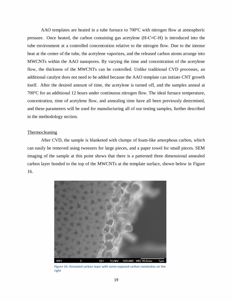
After CVD, the sample is blanketed with clumps of foam-like amorphous carbon, which
can easily be removed using tweezers for large pieces, and a paper towel for small pieces. SEM
imaging of the sample at this point shows that there is a patterned three dimensional annealed
carbon layer bonded to the top of the MWCNTs at the template surface, shown below in Figure
16.
Figure 16: Annealed carbon layer with some exposed carbon nanotubes on the right

20
Thermocleaning is used to expose the MWCNTs by removing the annealed carbon layer
via oxidation in a high temperature air filled furnace. It has been shown to burn off at a
temperature of 650°C, consistent with a crystalline, graphite-like structure (Xiaowei 2004).
Figure 17 below shows the top surface of a sample after thermocleaning at 650°C for 15,
20, and 30 minutes. These images show the progression of oxidation over time, slowly removing
the annealed carbon and exposing the template. At 20 minutes, the layer has almost been
completely removed, and at 30 minutes, the whole layer has been oxidized, along with the CNTs
underneath. Therefore, the time required to completely remove this layer while leaving the CNTs
intact should be between 20 and 30 minutes. Optimization of this parameter is required to
complete the heat sink design.
Etching
Once the annealed carbon layer is removed by thermocleaning, the surface of the AAO
template is exposed, with MWCNTs filling all the nanopores. In order to expose the tips of the
MWCNTs, a wet etching process can be used to dissolve the AAO substrate at the surface. The
acidic etching solution reacts with the surface molecules at a constant rate which results in linear
mass loss (Hu 2009). CNT protrusion length can be controlled by knowing the etching rate of a
particular acid and varying the etching time.
Figure 17: Incremental thermocleaning showing the removal of the annealed carbon layer at 15 min, 20 min, and 30min

21
The most common etchant of AAO template is NaOH, however this acid results in rapid
non-uniform removal of surface material. In order to produce protrusions which will not clump
together, a very thin layer of material must be removed evenly over the entire surface. A much
milder etchant is phosphoric acid (H3PO4) which reacts at a much slower rate and allows for a
larger amount of control (Hu 2009). The etching rate can be further controlled by varying the
concentration of the H3PO4 solution. High concentrations of H3PO4 such as a 10 wt% solution
have a much faster etching rate than a 3 wt% solution (Hu 2009).
To produce an array of MWCNT protrusions with a controlled aspect ratio without
clumping, a mild etchant must be used for a relatively short amount of time. To ensure that the
length of CNT protrusion is consistent over the entire sample a low concentration of H3PO4 such
as 3 wt% is ideal. To determine the etching time that results in this ideal protrusion length, a
parallel etching optimization process could be performed.
Imaging and Testing Methods
Creating an aligned MWCNT array heat sink demands sample imaging at extremely
small scales to collect data for the design optimization process. Logical and measurable testing
methods are necessary to measure the comparative effectiveness of a nano-scale heat sink.
Scanning Electron Microscope Imaging
The scanning electron microscope (SEM) has proven to be one of the most useful pieces
of equipment in a wide range of fields from biology to material science. The SEM is different
from conventional light microscopes, because electrons are used instead of photons. Since the
wavelength of an electron is significantly smaller, the SEM produces images with incredible
resolution. This means features spaced as close as 1-5 nm can still be distinguished separately.
In addition, SEMs have a very large depth of field which allows a large portion of the sample to
be in view at the same time.
The SEM image is generated by the interaction of electrons with the atoms on the sample
surface. The resulting deflections produce signals which contain information about the samples
topography and composition (Klesel 2009). The electron beam is generated by the electron gun,
which is typically composed of a tungsten cathode. A voltage is applied to the cathode which
causes the electrons to move towards the positively charged anode and down to the sample.

22
Before this beam reaches the sample it must be condensed and focused by magnetic lenses into a
very fine point. A final lens deflects this beam back and forth in a raster scan so the entire frame
can be viewed at once (Klesel 2009). Figure 18 shows the major components of a scanning
electron microscope.
When the electrons strike the
sample, they are scattered and absorbed
within a teardrop shaped interaction volume
which extends about 100 nm to 5 µm into
the surface. The electron deflections from
both elastic and inelastic scattering result in
a variety of interactions, the most useful
being secondary electrons and back-
scattered electrons, see Figure 19.
Secondary electrons originate from
within a few nanometers of the surface, and
the number of electrons detected depends
strongly of the angle of the surface features.
Since steep edges appear brighter, clear 3-D
topographical images can be produced
(Goldstein 1981). Back-scattered electrons
originate from deeper in the surface and the
amount deflected depends on the atomic
weight of the elements in the sample. The
result of this technique is an image with
varying shades from white to black corresponding
to different elements.
There are two conditions that must be
satisfied in order to produce a clear and readable
Figure 18: Major components of a scanning electron microscope
Figure 19: Electron surface interactions

23
image. First, the chamber from the electron source to the sample must be kept at a vacuum,
primarily to eliminate interactions between electrons and any gas particles which would
destabilize the beam. The other critical condition is that the sample surface must be electrically
conductive and grounded to prevent the accumulation of an electrostatic charge. If the sample is
not conductive already, a process called sputter coating can be used which deposits an ultrathin
coating of highly conductive metal to allow imaging (Klesel 2009).
SEM imaging is a crucial technique for our project since we need to examine surface
structure morphology at such small scales. Optimization of our manufacturing parameters will
require extensive SEM observations. Once the nano-scale surface morphology of each sample is
known, a comparative testing method can be performed.
Comparative Testing Method
Obtaining quantitative results for a nano-scale surface structure‟s convective properties
requires macro-scale measurement devices to be used in order to detect nano-scale phenomenon.
This presents a unique problem to scientists studying these systems. Concrete, accurate values
for material properties at the nano-scale are inherently difficult to verify with high certainty, so
comparative methods become a good way to acquire data with which to analyze nano-scale
systems. For our testing, tiny thermistors are used to record temperature measurements over
time. Under constant heating, we can obtain data for varied surface morphology, enabling
comparative analysis of the convective
properties.
The study on mixing randomly
dispersed CNTs into a thermal compound
discussed earlier used this type of
comparative method to measure steady-state
CPU temperature on varied samples under
controlled heat input and airflow, the results
of which are shown in Figure 20.
The level regions of the temperature
vs. time curves denote the steady state Figure 20: Difference in steady state temperature caused by mixing CNTs in silver paste compared to silver paste alone

24
temperatures. The CPU temperature vs. time curves for the thermal compound with and without
CNTs show that the addition of CNTs lowered steady state temperature. This comparative
analysis justifies the conclusion that mixing in CNTs increased the heat sinks performance
versus the thermal compound alone (Thang 2009). An expanded version of this deductive logic
will be incorporated into the comparative testing method for our project, to examine the effects
of aligned MWCNT arrays on convective heat transfer using the design, manufacturing, imaging,
optimization, and testing techniques described in this section
Methodology
Sample Preparation
CNT Growth
Before template assisted CVD growth, our AAO
templates needed to be cut into 4 mm x 7 mm samples, in
order to completely cover the strain gage‟s heating
element. Consistency was a focus, and only the most
accurate samples were selected to ensure comparable
testing. AAO templates were cut into 7 mm wide strips
using a scalpel and the clamping setup shown in Figure
21. This 7 mm strip was then cut again every 4 mm into
as many samples as possible.
Figure 21: Scalpel and clamping system used for cutting samples

25
Samples were loaded into a ceramic boat, which was then inserted into a one inch
diameter quartz tube furnace and centered, shown in Figure 22. Next, the ends of the tube were
connected to a controlled gas flow and vacuum system.
Once the seal between the tube and the gas flow system was created, its integrity was
tested using a procedure consisting of vacuum depressurization followed by pressurization by
means of nitrogen gas flow into the tube. The tube was first closed off from the atmosphere, and
then attached to a vacuum which was used to depressurize the tube to negative 0.5 bars. The
system was subjected to this vacuum for one minute, then the vacuum was turned off, and the
system was reopened to gradual nitrogen flow. The tube was then slowly re-pressurized with
nitrogen at a flow rate of about 60 mm on our flow meter, until pressure within the tube
exceeded atmospheric pressure, reaching 0.5 bars. The gas within the tube was then stabilized at
this pressure for about a minute. This pressurization procedure was repeated three times from
vacuum to 0.5 bars to ensure a good seal before beginning the chemical vapor deposition process
with the tube at atmospheric pressure.
The furnace was set to increase at a rate of 10°C per minute up to 700°C, and gradual
heating rate was used to avoid any effect of thermal shock on our samples. During heating,
nitrogen flowed through the tube at a rate of 60 mm. Once at the desired temperature, a
combined flow rate of nitrogen and acetylene was established by turning on the acetylene, and
Figure 22: Tube furnace system used for chemical vapor deposition

26
adjusting the total flow rate to our desired concentration. A mix of 80% nitrogen and 20%
acetylene was established using flow rates of 60 mm and 15 mm, respectively. This reaction
occurred for one hour, and then the acetylene was turned off. The sample was left in the tube
furnace to anneal at the set temperature for the next 12 hours. Once the annealing time was over,
the furnace was turned off and allowed to cool gradually before removing the ceramic boat full
of AAO templates, now with MWCNTs filling the nanopores and an annealed carbon layer on
the surface. When the boat first comes out, the samples are buried by amorphous carbon. Some
are concave up and some concave down coming out of the furnace as seen in Figure 23, which
shows that this curvature is determined by the
AAO template morphology, not the sample
orientation when MWCNTs are grown. The
samples had to be picked out using tweezers
and separated from the junk carbon. Excess
carbon was scraped off gently using a paper
towel, resulting in clean samples ready for
thermocleaning.
Thermocleaning Optimization
To optimize removal of the annealed carbon layer
from the template surface, a parallel optimization process
was used. Based on our prior knowledge of
thermocleaning, we decided to investigate the effect of
time at a temperature of 650ºC in the furnace pictured in
Figure 24.
Samples were loaded into a ceramic boat as
shown below in Figure 25, all concave down for
consistency. Incremental thermocleaning times from 20
to 30 minutes were performed on samples, since we
Figure 23: Samples after CVD with amorphous junk carbon on bottom
Figure 24: Furnace used for thermocleaning

27
previously knew there is still annealed carbon on the surface at 20 minutes, and the MWCNTs
themselves are burned off at 30 minutes.
Our first trial of thermocleaning
resulted in total carbon burnout at 22
minutes, but we realized that the furnace‟s
insulation was actually withholding
substantial heat between trials. To address
this, an hour was allowed for the furnace to
cool down between concurrent
thermocleaning trials. After resolving this
process issue, we were able to obtain very
good SEM images which provided us with
an optimal thermocleaning time which
fully removed the annealed carbon layer
while leaving the MWCNTs intact. Top
views of the sample surface morphologies for the incremental times were used for comparison.
The optimal morphology was seen at 28 minutes of thermocleaning, shown below in
Figure 26. The whitest regions in the image represent the peaks of the AAO template, uncovered
from the carbon layer. The MWCNTs can clearly be seen inside the pores.
Figure 25: Samples loaded in ceramic boat for thermocleaning
Figure 26: SEM image after 28 minutes of thermocleaning, showing exposed MWCNTs inside the nanopores

28
With a thermocleaning time established, an etching optimization procedure was performed, as
described below.
Etching Optimization
The amount of ceramic template dissolved from the top and bottom of the sample is a
function of time and acid concentration. A 0.5 Molar H3PO4 solution was chosen as the solvent
for etching the Al2O3 based on previous experimental work done within our facilities. Using the
same concentration, incremental times were tested in parallel.
Each etching consisted of submerging the
sample into our solution using a concave etching
platform elevated in a beaker with 500mL of solution
Figure 27. The concavity of the platform lets the
solution come in contact with both the top and bottom
surface of the sample. For the first trial of our
optimization, etching times were chosen to cover a wide
range, from a hardly etched short pillar sample up to a
substantially etched, long pillar sample. 10 min., 25
min., 1 hr., 2 hr., and 4 hr. intervals were chosen.
After the respective time, the sample was removed with tweezers and thoroughly rinsed
with distilled water. After drying, the samples were inspected using SEM. Results are shown
below in Figure 28. A comparison between the 25 minute and 4 hour sample is shown, both
showing slightly exposed MWCTs. Each sample was broken into tiny pieces, and there were
clear differences between different areas of the same sample. Observations of surface
morphology showed variation between different sections of the rectangles; perhaps the outside
edges were more etched.
Figure 27: Samples being acid etched on a concave surface

29
Figure 28: left: 25 minute etch, right: 4 hour etch
Comparative Testing
Testing Setup
For our testing setup, samples were stacked on top of a strain gage heater, with a thin
layer of silicon based thermal grease as the thermal interface material. To monitor the internal
temperature over time (Tinternal vs. time), a glass micro-bead thermistor (Figure 29), was mounted
underneath the heater. This tiny glass encapsulated piece of semiconductor varies in resistance
as temperature changes, and can be calibrated to give accurate temperature readings.
Figure 29: Micro-bead thermistor
30
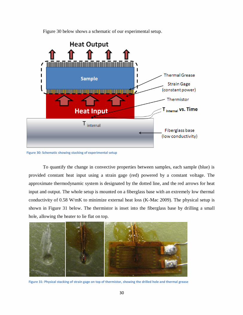
Figure 30 below shows a schematic of our experimental setup.
To quantify the change in convective properties between samples, each sample (blue) is
provided constant heat input using a strain gage (red) powered by a constant voltage. The
approximate thermodynamic system is designated by the dotted line, and the red arrows for heat
input and output. The whole setup is mounted on a fiberglass base with an extremely low thermal
conductivity of 0.58 W/mK to minimize external heat loss (K-Mac 2009). The physical setup is
shown in Figure 31 below. The thermistor is inset into the fiberglass base by drilling a small
hole, allowing the heater to lie flat on top.
Figure 31: Physical stacking of strain gage on top of thermistor, showing the drilled hole and thermal grease
Figure 30: Schematic showing stacking of experimental setup

31
To measure temperature using our thermistor, a circuit was built to measure the resistance
over time, which was then calibrated to determine temperature at a given resistance value. An
excitation voltage was applied to a voltage divider circuit, with the thermistor in series with a
known resistance value (120 Ω) strain gage, shown below in Figure 32. The excitation voltage
and the voltage across our known resistor were monitored over time using a virtual
instrumentation program, discussed later in this section. With this information, our program
calculated the resistance of the thermistor every 0.25 seconds and recorded the data to a
spreadsheet.
The physical circuit is shown below ready for testing, with a sample mounted and the
alligator clips connected (Figure 33).
Figure 33: Schematic of the voltage divider circuit used in our experiment
Figure 32: Physical circuit with alligator clips supplying voltage and monitoring resistance

32
This whole setup was covered with a plastic bin during the tests (Figure 34), which
greatly reduced airflow fluctuations within the room and maintained a steadier ambient
temperature. The alligator clips which supply power to the strain gage heater were connected to
the constant voltage source. The rest of the clips connected to our Data Acquisition device
(DAQ), which supplied an excitation voltage to the thermistor circuit, monitored that voltage,
and monitored the voltage across the known resistor.
Virtual Instrumentation
To perform the thermal testing necessary for our investigation, we first needed an
effective method to monitor the temperature over time via our thermistor. A virtual instrument
(VI) was created in National Instruments LabView for this purpose; the block diagram
programming logic is shown in Figure 35.
Figure 34: Testing setup covered by plastic bin to limit air fluctuations

33
Figure 36 below shows the equation used within our VI program to calculate the
resistance of the thermistor (R1) with respect to the excitation voltage (Vin) and the voltage
across the known 120Ω strain gage R2 (Vout).
Figure 35: Block diagram showing the programming logic of our virtual instrument
Figure 36: Voltage divider schematic and equation

34
From this equation, R1 = (R2*Vin / Vout) – R2. The section of our VI responsible for this
calculation is shown in Figure 37. Vin is channel 0, and Vout is channel 1, as denoted by the blue
boxed numbers. The division, multiplication, and subtraction boxes are the logic which executes
this formula to calculate R2, the thermistor resistance value.
The section of our programming logic shown below in Figure 38 enables our VI to read
resistance accurately at the large range of resistance values that are encountered in heating the
system. When the resistance of the thermistor is high, the voltage across the known resistor is
low, and vice versa for when the thermistor has a low resistance at hot temperatures. The
program accounts for this by adjusting the excitation voltage according to the thermistor
resistance.
Figure 37: Section of programming logic that performs the voltage divider equation
Figure 38: Section of programming logic which adjusts the excitation voltage to account for high resistances
35
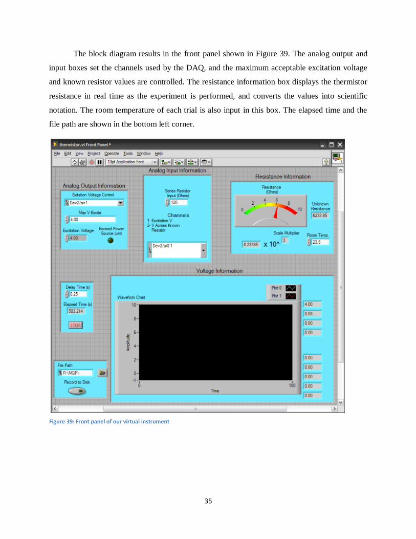
The block diagram results in the front panel shown in Figure 39. The analog output and
input boxes set the channels used by the DAQ, and the maximum acceptable excitation voltage
and known resistor values are controlled. The resistance information box displays the thermistor
resistance in real time as the experiment is performed, and converts the values into scientific
notation. The room temperature of each trial is also input in this box. The elapsed time and the
file path are shown in the bottom left corner.
Figure 39: Front panel of our virtual instrument
36
Thermal Testing Technique
Thermal testing was performed on many occasions for the different morphologies that
exist at each step in our sample preparation, and a blank heater with no sample on top as the
control. When the heater is activated, the Tinternal increases from room temperature up to a steady
state temperature, where the heat input approximately equals the heat output. When the heater is
turned off, the system will eventually reach room temperature again. The T internal vs. time data for
this process was collected for each sample, and steady state temperatures were compared. A
sample with better convective surface properties should have a lower steady state temperature.
To enable comparative analysis for our testing method, data was gathered for the AAO
template alone, the template with MWCNTs grown before thermocleaning (annealed carbon
surface layer), after thermocleaning (unexposed MWCNTs), and for thermocleaned then etched.
Between each trial, the entire setup was given a full hour to cool back down to room
temperature. Each sample trial included a 60 second run at room temperature, then another run
where the heater was activated after ten seconds of recording, and the data was recorded for
about 500 seconds.
Temperature Calibration
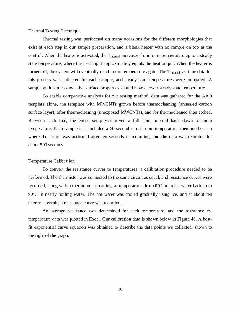
To convert the resistance curves to temperatures, a calibration procedure needed to be
performed. The thermistor was connected to the same circuit as usual, and resistance curves were
recorded, along with a thermometer reading, at temperatures from 0°C in an ice water bath up to
90°C in nearly boiling water. The hot water was cooled gradually using ice, and at about ten
degree intervals, a resistance curve was recorded.
An average resistance was determined for each temperature, and the resistance vs.
temperature data was plotted in Excel. Our calibration data is shown below in Figure 40. A best-
fit exponential curve equation was obtained to describe the data points we collected, shown to
the right of the graph.
37
Figure 40: Thermistor calibration graph with best fit equation
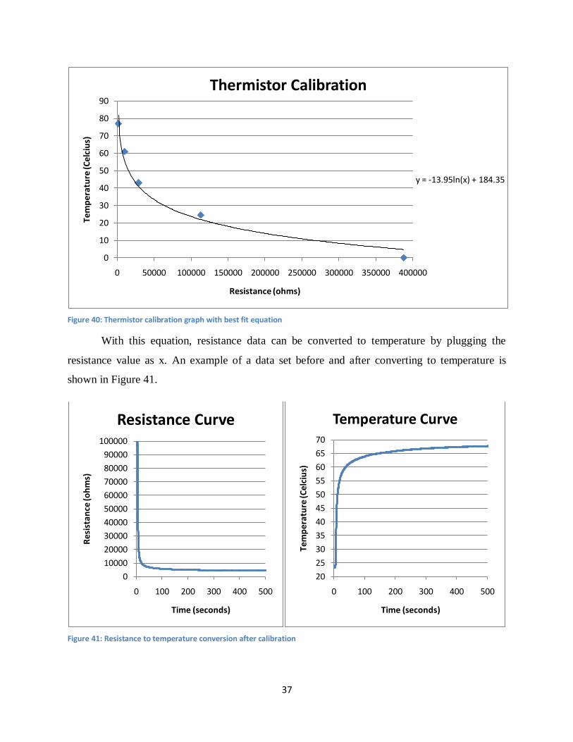
With this equation, resistance data can be converted to temperature by plugging the
resistance value as x. An example of a data set before and after converting to temperature is
shown in Figure 41.
Figure 41: Resistance to temperature conversion after calibration
y = -13.95ln(x) + 184.35
0
10
20
30
40
50
60
70
80
90
0 50000 100000 150000 200000 250000 300000 350000 400000
Tem
pe
ratu
re (C
elc
ius)
Resistance (ohms)
Thermistor Calibration
0
10000
20000
30000
40000
50000
60000
70000
80000
90000
100000
0 100 200 300 400 500
Res
ista
nce
(oh
ms)
Time (seconds)
Resistance Curve
20
25
30
35
40
45
50
55
60
65
70
0 100 200 300 400 500
Tem
per
atu
re (C
elc
ius)
Time (seconds)
Temperature Curve
38
Results and Analysis
Over 12 days of testing, we produced a quantity of results to be processed and analyzed.
Our first objective was to ensure that our testing method was repeatable, and that the results from
different morphologies were distinguishable. For clarity, Table 1 below designates the
abbreviations that will be used for the different samples.
Sample Morphology Abbreviation
Heater alone Blank
AAO template alone Temp
Template with MWCNTs grown Unthermo
Template with MWCNTs grown, and
thermocleaned Thermo
Template with MWCNTs grown,
thermocleaned, and etched Etched
Table 1: Morphologies tested with abbreviations
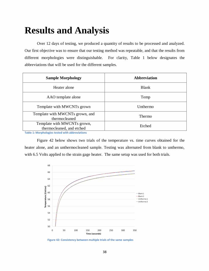
Figure 42 below shows two trials of the temperature vs. time curves obtained for the
heater alone, and an unthermocleaned sample. Testing was alternated from blank to unthermo,
with 6.5 Volts applied to the strain gage heater. The same setup was used for both trials.
Figure 42: Consistency between multiple trials of the same samples

39
This graph shows consistency between trials with the same morphology, and a clear
difference between the heater alone and with a sample on top. The steady state temperature of
the unthermocleaned sample is about one degree Celsius lower than that of the blank heater. This
shows that heat is moving more easily through the sample than from the heater to air alone,
therefore working as a heat sink. The curves never truly reach a constant steady state
temperature, since some heat is transferred and stored in the fiberglass base, which has an
extremely low, but not negligible thermal conductivity.
Three examples of the cool-down section of the curve are shown below in Figure 43, but
they are virtually indistinguishable due to the data acquisition device‟s bit size capabilities, so
this portion of the curve was not recorded in consequent trials.
Figure 43: Cool down curves after heater is turned off

40
The next graph (Figure 44) shows a blank heater, an empty template, and two different
etched samples. At a higher voltage of 7.5 V, the steady state temperature differences between
samples are more obvious, due to the exponential curve used to calibrate to temperature. Both
etched samples have lower steady state temperatures than the template, but they show significant
differences with each other. The slope of the steady state portion of the curve is approximately
equal between the etched samples, both lower compared with the slopes seen in the template and
the blank curves. It appears that the etched samples outperformed the template in terms of heat
transfer efficiency to the surrounding air, but the difference between the two etched samples
could be due to the sample mounting (thermal grease layer thickness, possible air pockets, or
thermal contact area with heater), or the length of exposed CNT tips.
Relative performance differences were seen between similar samples throughout all the
trials, but there are relevant consistencies within the entire data set, and the inconsistencies seen
Figure 44: Temperature vs. time curves for blank, template, and two different etched samples

41
could be due to a variety of uncontrollable factors. Figure 45 below shows three complete sets of
comparative morphology data.
The relative positions of the blank heater (dark blue), empty template (red), and
unthermocleaned (light blue) are the same in each of the trials. These are the most consistent
samples since there is no additional processing after CNT growth. The thermocleaned and etched
samples vary in their relative position between trials, likely caused by subtle differences in their
processing parameters. In the left (4.5 V), thermo and etched did not perform as well as the
empty templates, possibly indicative of excess thermocleaning time. For the center and right
trials (5.5 V), the thermocleaning time was reduced from 28 to 27.5 minutes. The etched sample
was the most effective in the center trial, but this behavior was not seen elsewhere in our testing.
This could be due to minor morphology differences or inconsistent thermal connections between
sample and heater. In the right trial, thermo and etched both fell between the template and the
unthermo sample, with thermo lower than etched. Again, this could be due to sample mounting
differences, or perhaps combustion of the CNTs due to excess thermocleaning.
Figure 45: Comparative analysis of all tested morphologies for three separate trials
42
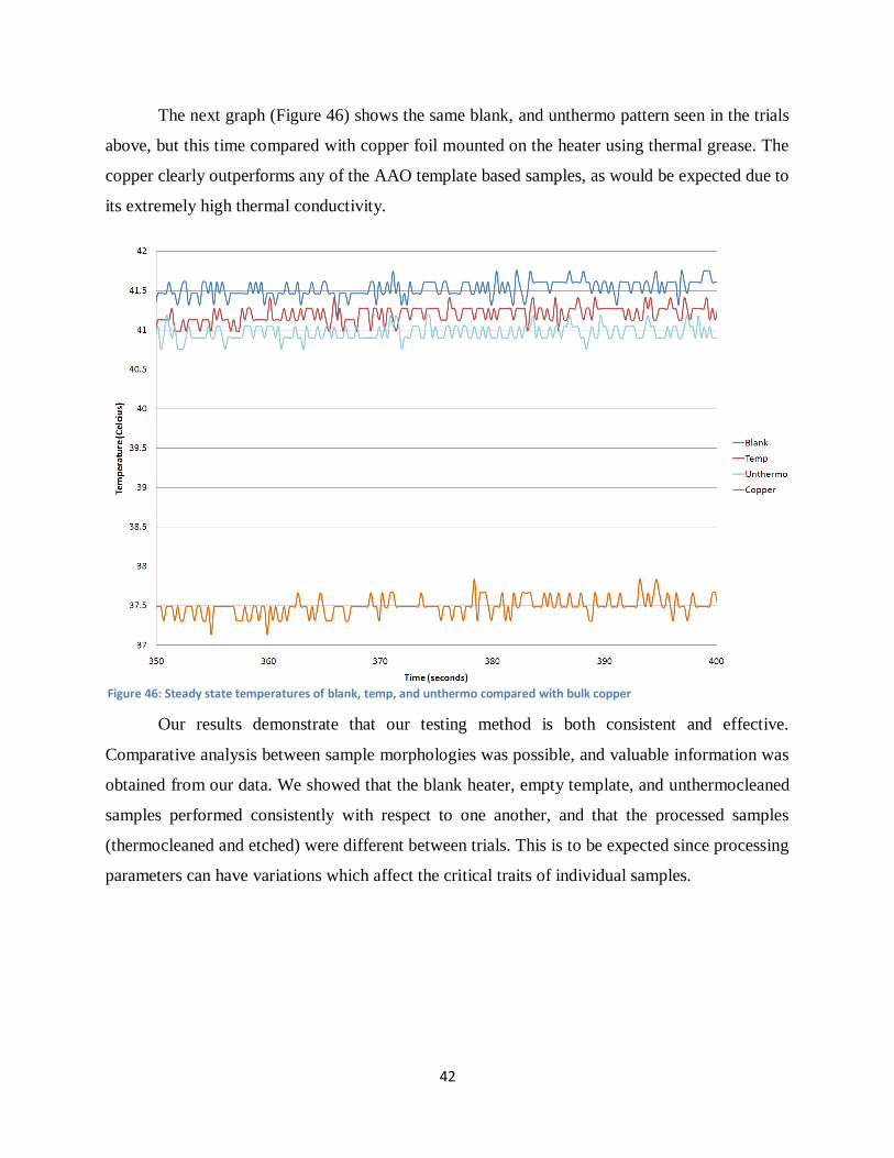
The next graph (Figure 46) shows the same blank, and unthermo pattern seen in the trials
above, but this time compared with copper foil mounted on the heater using thermal grease. The
copper clearly outperforms any of the AAO template based samples, as would be expected due to
its extremely high thermal conductivity.
Our results demonstrate that our testing method is both consistent and effective.
Comparative analysis between sample morphologies was possible, and valuable information was
obtained from our data. We showed that the blank heater, empty template, and unthermocleaned
samples performed consistently with respect to one another, and that the processed samples
(thermocleaned and etched) were different between trials. This is to be expected since processing
parameters can have variations which affect the critical traits of individual samples.
Figure 46: Steady state temperatures of blank, temp, and unthermo compared with bulk copper

43
Conclusions
After performing our experiments, we were able to obtain some clear results and
conclusions about the heat transfer properties of our nano-structured surfaces to the ambient air.
Even though the AAO templates have a known thermal conductivity of 40 W/mK, growing
MWCNTs which have a lower thermal conductivity of 10 W/mK, still enhanced heat transfer.
Our results suggest that there are definitely some unique heat transfer properties due to the nano-
scale three-dimensional annealed carbon layer. The processed samples were less predictable,
since minor differences in processing parameters can cause variations which affect the
performance of individual samples. These inconsistencies are difficult to avoid, since the
variations in processing are sometimes out of the range which we can accurately control.
Unthermocleaned samples were shown to consistently have the best convective heat transfer
properties.
Future research could potentially narrow down the uncertainty we observed, and the
processing parameters have potential to be further optimized for better results. Also, there are
many other CNT morphologies that could be used effectively for this type of micro and nano
scale heat transfer. Different manufacturing techniques altogether or further improvements of our
native processes could be a part of improving these results. As electronics continue their trend of
miniaturization, investigation of nano scale convection properties are sure to continue. We are
happy to help open this window for future progress, and look forward to continued research in
the area.

44
Bibliography
Belwalkar, A., E. Grasing, W. Van Geertruyden, Z. Huang, and W. Z. Misiolek. "Effect of
Processing Parameters on Pore Structure and Thickness of Anodic Aluminum Oxide
(AAO) Tubular Membranes." Journal of Membrane Science 2nd ser. 319.1 (2008): 192-
98. Print.
"Carbon, its Allotropes and Structures." EveryScience. Web. 11 Dec. 2009.
<http://www.everyscience.com/Chemistry/Inorganic/Carbon/a.1189.php>.
Conway, Paul, David Whalley, and Farhad Sarvar. "Thermal Interface Materials - A Review of
the State of the Art." Electronics Systemintegration Technology Conference (2006):
1292-302.
Demczyk, B. G., Y. M. Wang, J. Cumings, M. Hetman, W. Han, A. Zettl, and R. O. Ritchie.
"Direct Mechanical Measurement of the Tensile Strength and Elastic Modulus of
Multiwalled Carbon Nanotubes." Materials Science and Engineering A334 (2002): 173-
78.
"Fiberglass Sheets and Plates by K-mac Plastics." Plastic Sheets, Rods and Tubes by K-mac.
Web. 07 Dec. 2009. <http://k-mac-plastics.com/fiberglass-sheet.htm#VO>.
Garimella, Suresh. "Advances in mesoscale thermal management technologies for
microelectronics." Microelectronics Journal 37 (2006): 1165-185. Print.
Goldstein, G. I., D. E. Newbury, P. Echlin, D. C. Joy, C. Fiori, and E. Lifshin. Scanning Electron
Microscopy and X-Ray Microanalysis a Text for Biologists, Materials Scientists, and
Geologists. New York: Plenum, 1981.
Hong, Seunghun, and S. Myung. "Nanotube Electronics: A Flexible Approach to Mobility."
Nature Nanotechnology 2.4 (2007): 207-08.
Hu, Guofeng, Haiming Zhang, Wenwen Di, and Tingting Zhao. "Study on Wet Etching of AAO
Template." Applied Physics Research 1.2 (2009): 78-82. Print.
Jimenez, Guillermo A., and Sadhan C. Jana. "Electrically Conductive Polymer Nanocomposites
of Polymethylmethacrylate and Carbon Nanofibers Prepared by Chaotic Mixing."
Composites: Part A 38 (2007): 983-93. Print.
Kim, P., L. Shi, A. Majumdar, and P. L. McEuen. "Thermal Transport Measurements of
Individual Multiwalled Nanotubes." Physical Reviews Letters 87.21 (2001).
Klesel, Josh. "Scanning Electron Microscopy." Materials Science and Engineering. Iowa State
University. Web. 25 Nov. 2009. <http://mse.iastate.edu/microscopy/home.html>.

45
Kordas, K., G. Toth, P. Moilanen, M. Kumpumaki, J. Vahakangas, A. Uusimaki, R. Vajtai, and
P.M. Ajayan. "Chip cooling with integrated carbon nanotube microfin architectures."
Applied Physics Letters 90.123105 (2007). Print.
Li, C. Papadopoulos, J. M. Xu, and M. Moskovits, Appl. Phys. Lett. 75, 367 s1999d.
Li, Jun, and Meyya Meyyappan. Nanoengineered Thermal Materials Based on Carbon Nanotube
Array Composites. The United States of America as Represented by the Administrator of
the National Aeronautics and Space Administration, assignee. Patent 7,273,095 B2. 25
Sept. 2007.
Lu, Shijing, Zixue Su, Jian Sha, and Wuzong Zhou. "Ionic nano-convection in anodization of
aluminum plate." ChemComm (2009): 5639-641. Print.
Melechko, A. V., V. I. Merkulov, T. E. McKnight, M. A. Guillorn, K. L. Klein, D. H. Lowndes,
and M. L. Simpson. "Vertically Aligned Carbon Nanofibers and Related Structures:
Controlled Synthesis and Directed Assembly." Applied Physics Reviews 97 (2005).
Naeemi, Azad, and James D. Meindl. "Carbon Nanotube Interconnects." Proc. of 2007
International Symposium on Physical Design, Austin, Texas, USA. Print.
"Nanotechnologies: Carbon nanotubes." Rob Aid presents robots, gadgets. tech and bionics.
Web. 11 Dec. 2009. <http://www.robaid.com/tech/nanotechnologies-carbon-
nanotubes.htm>.
Ngo, Quoc, Brett Cruden, Alan Cassell, Gerard Sims, M. Meyyappan, Jun Li, and Cary Yang.
"Thermal Interface Properties of Cu-filled Vertically Aligned Carbon Nanofiber Arrays."
Nano Letters 4.12 (2004): 2403-407. Print.
Page, M. "Intel Stock Core 2 Duo Radial Curved Bifurcated Fin Heatsink Review." Frosty Tech.
2009. Web. <http://www.frostytech.com/articleview.cfm?articleID=2132>.
Pradhan, N.R., H. Duan, J. Liang, and G.S. Iannacchione. "Specific heat and thermal
conductivity measurements for anisotropic and random macroscopic composites of cobalt
nanowires." Nanotechnology 19 (2008). Print.
Prasher, Ravi. "Thermal Interface Materials: Historical Perspective, Status, and Future
Directions." Proceedings of the Institute of Electronics and Electronics Engineers 94.8
(2006): 1571-586. Print.
Shaikh, Shadab, Khalid Lafdi, and Edward Silverman. "The effect of a CNT interface on the
thermal resistance of contacting surfaces." Carbon 45 (2007): 695-703. Print.
Son, Won Il, Joo-Hee Hong, and Jae-Min Hong. Fabrication of micro-heat sink by nanotemplate
synthesis and its cooling characteristics. Rep. Cheongryang, Seoul, Korea:

46
Optoelectronic Materials Research Center, Korea Institute of Science and Technology,
2005. Print.
"Space Elevator Concept." The LiftPort Space Elevator. LiftPort Group. Web. 10 Dec. 2009.
<http://www.liftport.com/>.
Thang, Bui Hung, Phan Ngoc Hong, Phon Hong Khoi, and Phon Ngac Minh. "Application of
multiwall carbon nanotubes for thermal dissipation in a micro-processor." Institute of
Physics Electronic Journals. 2009. Web.
Thostenson, Erik T., Zhifeng Ren, and Tsu-Wei Chou. "Advances in the Science and
Technology of Carbon Nanotubes and Their Composites: A Review." Composites
Science and Technology 61 (2001): 1899-912.
Varanasi, Kripa, Tao Deng, Pramod Chamarthy, Shakti Chauhan, Peter De Bock, Ambarish
Kulkarni, Gary Mandrusiak, Brian Rush, Boris Russ, Lauraine Denault, Stanton Weaver,
Frank Gerner, Quinn Leland, and Kirk Yerkes. Nanostructures for High Thermal
Conductivity Substrates. Tech. Cambridge, MA, Nisakayuna, NY, Cinncinnati, OH,
Dayton, OH: Massachusetts Institute of Technology, GE Global Research Center,
University of Cinncinnati, Air Force Research Lab, 2008.
Vasiliev, L.L. "Micro and miniature heat pipes – Electronic component coolers." Applied
Thermal Engineering 26 (2008): 266-73. Print.
Wilson, Mick, Kamali Kannangara, Geoff Smith, Michelle Simmons, and Burkhard Raguse.
Nanotechnology Basic Science and Emerging Technologies. Boca Raton, Fla: Chapman
& Hall/CRC, 2002.
Xiaowei, Luo, Robin Jean-Charles, and Yu Suyuan. "Effect of temperature on graphite oxidation
behavior." Nuclear Engineering and Design 227 (2004): 273-80.
Zhang, K., Y. Chai, M.M.F. Yuen, D.G.W. Xiao, and P.C.H. Chan. "Carbon nanotube thermal
interface material for high-brightness light-emitting-diode cooling." Nanotechnology 19
(2008). Print.