nanohole grating as a refractive index sensor - politesi · a characterization of nanohole grating...
TRANSCRIPT
Politecnico di Milano
Facolta di Ingegneria dei Processi IndustrialiDegree in Materials Engineering
A Characterization of NanoholeGrating Refractive Index Sensors
for Biosensing Applications
A Thesis Submitted to the Faculty of
Politecnico di Milano by
Alyssa Bellingham
Matricola: 781868
Advisor Dr. Carlos Angulo Barrios
Universidad Politecnica de Madrid, Madrid, Espana
Co-Advisor Dr. Adam Fontecchio
Drexel University, Philadelphia, Pennsylvania, United States of America
Co-Advisor Dr. Maria Cristina Tanzi
Politecnico di Milano, Milano, Italia

Academic Year 2011-2012

© Copyright November 2012
Alyssa A. Bellingham. All Rights Reserved.

For the wonderful friends I have made during my travels

Contents
List of Figures vi
Acknowledgements ix
Abstract xiii
Estratto in lingua italiana xvii
1 Introduction 1
1.1 Motivation . . . . . . . . . . . . . . . . . . . . . . . . . . . . . . 1
1.2 Contribution . . . . . . . . . . . . . . . . . . . . . . . . . . . . . 2
1.3 Thesis Outline . . . . . . . . . . . . . . . . . . . . . . . . . . . . 4
2 Biosensing with Nanohole Arrays 5
2.1 Biosensor Classification . . . . . . . . . . . . . . . . . . . . . . . 5
2.1.1 Recognition Element . . . . . . . . . . . . . . . . . . . . 5
2.1.2 Transduction Element . . . . . . . . . . . . . . . . . . . 6
2.1.3 Label-Based vs. Label-Free Detection . . . . . . . . . . . 6
2.2 Refractive Index(RI) Sensing . . . . . . . . . . . . . . . . . . . . 7
2.2.1 Extraordinary Optical Transmission(EOT) . . . . . . . . 9
2.2.2 Transmission Spectroscopy . . . . . . . . . . . . . . . . . 10
2.3 Factors Effecting RI Sensing . . . . . . . . . . . . . . . . . . . . 10
2.3.1 Rayleigh Anomalies(RAs) . . . . . . . . . . . . . . . . . 10
2.3.2 Surface Plasmon Polariton-Bloch Waves(SPP-BW) . . . 11
2.3.3 Rayleigh Anomaly-Surface Plasmon Polaritons(RA-SPPs) 12
2.4 Chapter Summary . . . . . . . . . . . . . . . . . . . . . . . . . 13
3 Materials and Methods of Characterization 15
3.1 Nanohole gratings fabricated on metallic substrates . . . . . . . 15
3.1.1 Fabrication of gratings . . . . . . . . . . . . . . . . . . . 15
i
3.1.2 Nanohole Grating Solvent Characterization . . . . . . . . 17
3.1.3 Deposited Film Thickness Sensitivity . . . . . . . . . . . 19
3.1.4 Polarization Effect . . . . . . . . . . . . . . . . . . . . . 19
3.2 Biomolecule Recognition Element . . . . . . . . . . . . . . . . . 20
3.2.1 Surface Functionalization . . . . . . . . . . . . . . . . . . 21
3.2.2 Detection Protocol . . . . . . . . . . . . . . . . . . . . . 21
3.3 Molecularly Imprinted Polymer(MIP) Recognition Element . . . 22
3.3.1 Fabrication . . . . . . . . . . . . . . . . . . . . . . . . . 22
3.3.2 Detection Protocol . . . . . . . . . . . . . . . . . . . . . 23
3.4 Characterization Equipment . . . . . . . . . . . . . . . . . . . . 24
3.4.1 Spectrophotometer . . . . . . . . . . . . . . . . . . . . . 24
3.4.2 Fluorescent Microscope . . . . . . . . . . . . . . . . . . . 25
3.4.3 Filmetrics . . . . . . . . . . . . . . . . . . . . . . . . . . 26
3.5 Chapter Summary . . . . . . . . . . . . . . . . . . . . . . . . . 27
4 Theoretical 29
4.1 Finite-Difference Time-Domain(FDTD) Simulations . . . . . . . 29
4.1.1 Lumerical Software . . . . . . . . . . . . . . . . . . . . . 30
4.1.2 Simulation Results . . . . . . . . . . . . . . . . . . . . . 33
4.2 Origin of transmission spectra . . . . . . . . . . . . . . . . . . . 34
4.2.1 Hole Geometry . . . . . . . . . . . . . . . . . . . . . . . 36
4.3 Coupling Light into a waveguide . . . . . . . . . . . . . . . . . . 37
4.4 Chapter Summary . . . . . . . . . . . . . . . . . . . . . . . . . 38
5 Experimental Results 41
5.1 Solvent Characterization Results . . . . . . . . . . . . . . . . . . 41
5.2 Thickness Sensitivity . . . . . . . . . . . . . . . . . . . . . . . . 41
5.3 Polarization . . . . . . . . . . . . . . . . . . . . . . . . . . . . . 43
5.4 Biomolecule detection . . . . . . . . . . . . . . . . . . . . . . . . 43
5.5 MIP Molecule Detection . . . . . . . . . . . . . . . . . . . . . . 44
5.6 Chapter Summary . . . . . . . . . . . . . . . . . . . . . . . . . 44
6 Discussion 53
6.1 Solvent Characterization . . . . . . . . . . . . . . . . . . . . . . 53
6.2 Deposited Layer Thickness . . . . . . . . . . . . . . . . . . . . . 54
6.3 Biosensing Capabilities . . . . . . . . . . . . . . . . . . . . . . . 55
6.4 Chapter Summary . . . . . . . . . . . . . . . . . . . . . . . . . 56

7 Conclusions 57
7.1 Future Work . . . . . . . . . . . . . . . . . . . . . . . . . . . . . 57
Bibliography 59


List of Figures
2.1 Refraction of waves . . . . . . . . . . . . . . . . . . . . . . . . . 8
2.2 Diffraction at small aperature . . . . . . . . . . . . . . . . . . . 9
2.3 Schematic of Nanohole Array . . . . . . . . . . . . . . . . . . . 11
3.1 SEM 1µm pitch . . . . . . . . . . . . . . . . . . . . . . . . . . . 17
3.2 SEM 500nm pitch . . . . . . . . . . . . . . . . . . . . . . . . . . 18
3.3 Polarized Light . . . . . . . . . . . . . . . . . . . . . . . . . . . 20
3.4 Covalent vs. Non-covalent MIP binding . . . . . . . . . . . . . . 23
3.5 Example transmission spectrum . . . . . . . . . . . . . . . . . . 25
3.6 Filmetrics F20 Reflectance Spectrum . . . . . . . . . . . . . . . 26
4.1 Yee’s cell . . . . . . . . . . . . . . . . . . . . . . . . . . . . . . . 31
4.2 FDTD region . . . . . . . . . . . . . . . . . . . . . . . . . . . . 32
4.3 500 nm Theoretical spectral comparison . . . . . . . . . . . . . 33
4.4 500 nm Theoretical Solvent Characterization . . . . . . . . . . . 34
4.5 1 µm Theoretical spectral comparison . . . . . . . . . . . . . . . 35
4.6 1 µm Theoretical Solvent Characterization . . . . . . . . . . . . 36
4.7 1 µm Theoretical Layer Thickness Effect(<100 nm) . . . . . . . 37
4.8 1 µm Theoretical Layer Thickness Effect(<100 nm) . . . . . . . 38
4.9 1 µm Theoretical Layer Thickness Effect(>200 µm) . . . . . . . 39
4.10 Pitch Optimization . . . . . . . . . . . . . . . . . . . . . . . . . 40
5.1 1µ pitch grating spectral comparison . . . . . . . . . . . . . . . 42
5.2 1µm grating bulk sensitivity . . . . . . . . . . . . . . . . . . . . 43
5.3 500nm pitch grating spectral comparison . . . . . . . . . . . . . 44
5.4 500nm grating bulk sensitivity . . . . . . . . . . . . . . . . . . . 45
5.5 500nm grating thickness effect . . . . . . . . . . . . . . . . . . . 46
5.6 500nm grating thickness effect . . . . . . . . . . . . . . . . . . . 46
5.7 1µm grating thickness effect on spectrum of thick layers . . . . . 47
5.8 1µm grating thickness effect on spectrum of thin layers . . . . . 47
v

5.9 1µm grating thickness vs. wavelength of thick layers . . . . . . . 48
5.10 1µm grating thickness vs. wavelength of thin layers . . . . . . . 48
5.11 Polarization Effect . . . . . . . . . . . . . . . . . . . . . . . . . 49
5.12 Biomolecule Recognition . . . . . . . . . . . . . . . . . . . . . . 49
5.13 MIP with template molecules . . . . . . . . . . . . . . . . . . . 50
5.14 MIP without template molecules . . . . . . . . . . . . . . . . . 50
5.15 MIP after incubation . . . . . . . . . . . . . . . . . . . . . . . . 51
5.16 MIP after wash . . . . . . . . . . . . . . . . . . . . . . . . . . . 51
5.17 NIP . . . . . . . . . . . . . . . . . . . . . . . . . . . . . . . . . 52


Acknowledgements
I would like to start by thanking my parents Kathleen and Jeffrey Belling-
ham for their unwavering support, trust, and encouragement in me and my
dreams. I thank my sister, Kate, for always being able to make me laugh
and my brother, John, for allowing me to think I might have had some influ-
ence on his decision to become an engineer. I would like to thank Paul for
always supporting me and being extremely patient with my short temper and
busy schedule. I thank my grandparents for inspiring me to reach outside my
horizons and explore the world.
I would like to acknowledge my research advisor at Drexel University, Dr.
Adam Fontecchio, for his all his support and advice over the past five years.
Dr. Fontecchio and Drexel University have provided me many opportunities
above those typically available to students, including the opportunity to com-
plete the work for this Master’s degree in America, Italy and Spain as part of
the EAGLES program. My research advisor’s unwavering support and trust
in me is what has allowed me to pursue my research interests, forge interna-
tional collaborations, and attend local and international conferences. Without
his support, I would not be completing this degree and continuing my educa-
tion as an National Science Foundation Graduate Research Fellow at Drexel
University in the upcoming year.
I would like to thank my research advisor at Universidad Politecnica de
Madrid(UPM), Dr. Ing. Carlos Angulo Barrios, for welcoming me into his lab
to complete the research for this project. He was always available for discussion
and took an active interest in the project. His support, advice and feedback
have been invaluable during this project.
I would also like to thank Vctor Canalejas Tejero for all his help and ad-
vice on this project. He taught me everything I needed to know about the
fabrication and characterization equipment in the lab, fabricated all the grat-
ings for this project, and provided helpful insight and feedback on my work. I
ix

would never have been able to complete this project without all of his help. I
would also like to acknowledge Sonia Harranz and Sergio Carrasco for all their
help with the chemistry aspects of the project. They have been invaluable
in preparing the recognition elements(MIP and biomolecules)for this project.
Gracias!
I would like to thank the members of my committee from Politecnico de
Milano, Dr. Maria Cristina Tanzi, and Dr. Marco Ormelese for their feedback
on my thesis. I really value their insight and appreciate the feedback.
I would also like to thank all my colleagues in the Drexel Nanophoton-
ics lab in Philadelphia, USA, who have supported me in my research ca-
reer through discussion and joint project work including Dr.Kashma Rai, Dr.
Sameet Shriyan, Mr. Jared Coyle, Mr. Ben Pelleg, Ms. Elizabeth Plowman,
Ms. Yang Gao, and Ms. Sylvia Herbert. I would also like to acknowledge all
my other labmates who have provided a friendly and supportive research en-
vironment including Dr. Anna Fox, Dr. David Delaine, Ms. Jamie Kennedy,
Mr. Yohan Seepersad, and Mr. Bill Hicks. Tambin me gustara agradecer a
todos mis colegas en el laboratorio de la UPM ISOM que me han ayudado en
este proyecto y nos hizo mi breve tiempo en Espaa muy agradable. Grazie a
tutti i miei amici in Italia che mi hanno sostenuto durante questa ricerca.
I would like to acknowledge the Engineers As Global Leaders for Energy
Sustainability (EAGLES) program and all the people involved for providing
me with the opportunity to complete this degree across three countries. I
would especially like to thank Marcia Henisz, Holly Burnside, Amy Campbell,
and Michela Gregori for all their support and help during this program.
Last but certainly not least, I thank Dr. Selcuk Gucieri for mentoring and
supporting me since the first day I met him while visiting Drexel on a college
visit. He has provided me with more opportunities than I can count and has
always encouraged me to pursue my research and academic interests.


Abstract
Sub-wavelength periodic structures imprinted in metallic films give rise to en-
hanced transmission features which are sensitive to changes in refractive index
at the surface. Variations in the transmission spectral output can be quanti-
fied to detect the concentration of analyte in a solution and the surface of the
film can be readily modified with a variety of synthetic recognition elements,
biomolecules, and well-established silane chemistry to allow for molecule recog-
nition at the surface of the grating. These nanohole gratings can also be used
to couple light into planar optical waveguides, which make ideal signal trans-
ducers because of their sturdiness, easy patterning of reagents, and easy in-
corporation of polymer materials. This thesis seeks to characterize nanohole
structures imprinted on aluminum thin films as refractive index sensors that
can be incorporated as transduction elements into biosensing technologies as
well as to provide a path to optimization of an integrated biosensing device.
Aluminum, a previously unexamined material for these nanohole array im-
printed devices, was used as the metallic thin film in this thesis. The material
demonstrated similar enhanced transmission effects to well known plasmonic
materials like silver and gold, which cost significantly more than aluminum.
The aluminum film was imprinted with a periodic nanoscale array of holes us-
ing an etching procedure, and then evaluated as a refractive index sensor. The
bulk sensitivity of the nanohole array samples was determined through solvent
characterization as well as exposure to varying thicknesses of a deposited layer
of polymer. The ability of the potential transduction element to detect affinity
reactions occurring at the surface was evaluated using well known biomolecu-
lar recognition experiments as well as synthetic recognition experiments using
molecularly imprinted polymer films (MIPs).
MIPs are biomimetic recegnition elements that can be created for a variety
of molecular structures, enable large-scale chip fabrication, are reusable, and
offer superior stability when exposed to solvents and temperature extremes.
xiii

The potential to combine the nanohole array transducer element with this
synthetic recognition element is examined in this thesis. A theoretical opti-
mization of the grating pitch for optimal detection capability was performed
and the future path of optimizing an integrated biosensing device is discussed.


Estratto in lingua italiana
Le strutture periodiche di lunghezza donda inferiore impresse in film metallici
danno origine a caratteristiche migliorate di trasmissione che sono sensibili alle
variazioni dell’indice di rifrazione sulla superficie. Le variazioni nellemissione
spettrale possono essere quantificate per rilevare la concentrazione di analita
in una soluzione e la superficie del film pu essere facilmente modificata con
una variet di elementi di riconoscimento sintetici, biomolecole e applicando
la ben consolidata chimica del silano al fine di consentire il riconoscimento
della molecola alla superficie della griglia. Questi reticoli nanohole possono
essere utilizzati anche per indirizzare la luce in guide donda ottiche piane, il
che li rende trasduttori di segnale ideali a causa della loro robustezza, della
facile schematizzazione dei reagenti, e della facile integrabilit con materiali
polimerici. Questa tesi cerca di caratterizzare strutture nanohole impresse su
film sottili di alluminio come sensori di indice di rifrazione che possono essere
incorporati come elementi di trasduzione in tecnologie di biopercezione e per
fornire un percorso di ottimizzazione di un dispositivo integrato di biosensori.
Alluminio, un materiale precedentemente inesplorato per questi dispositivi
di matrice nanohole impressa, stato utilizzato come film metallico sottile e
ha dimostrato effetti similari a ben noti materiali plasmonici come l’argento
e l’oro, che costano molto di pi rispetto all’alluminio, nel miglioramento nella
trasmissione,. Il film di alluminio stato stampato con un ordinamento nano-
metrico periodico di fori utilizzando una procedura di incisione, e quindi valu-
tato come un sensore di indice di rifrazione. La sensibilit bulk dei campioni di
matrice nanohole stata determinata attraverso la caratterizzazione del solvente
cos come attraverso l’esposizione a diversi spessori di uno strato di polimero de-
positato. La capacit dell’elemento di trasduzione di rilevare reazioni di affinit
che si verificano in corrispondenza della superficie stata valutata utilizzando
ben noti esperimenti di riconoscimento biomolecolare nonch esperimenti di ri-
conoscimento sintetico usando dei molecularly impressed polymer films (MIP).
xvii

I MIP sono recettori biomimetici che possono creare recettori per una variet
di strutture molecolari, abilitare la fabbricazione di chip su larga scala, sono
riutilizzabili, e offrono una stabilit superiore quando esposti a solventi e a tem-
perature estreme. La potenzialit di combinare lelemento trasduttore a strut-
tura nanohole con lelemento di riconoscimento sintetico viene qui esaminata.
Una ottimizzazione teorica del passo di griglia per la capacit di rilevazione otti-
male stata eseguita e il percorso futuro di ottimizzare un dispositivo integrato
di biorilevamento discusso.


Chapter 1
Introduction
1.1 Motivation
There is a great need for powerful analytical and diagnostic tools in biomed-
ical industries for identifying diseases, monitoring biomolecular interactions,
and improving diagnostic tests. Compact devices integrating biological or bi-
ologically derived recognition elements with physiochemical transducers, or
biosensors, provide a means of achieving such tools. Biosensors are able to
rapidly detect trace quantities of biomolecules such as viruses,1 drugs,2 air-
bourne and waterbourne pathogens,3 and lipid bilayers.4 In the past 20 years,
biosensors have also become an established method of measuring molecular
interactions. However, biosensing technology is still limited by many factors
including, cost, efficiency, manufacturing procedures, speed, and sensitivity.
These limitations arise from the individual biosensor components as well as
their interaction with each other.
Plasmonic materials, such as gold and silver, can support surface electro-
magnetic oscillations, known as surface plasmon polaritons (SPPs). Theses
SPPs be excited by incident light in a resonant manner giving rise to sur-
face plasmon resonances (SPRs) that are sensitive to changes in the dielec-
tric material in contact with the surface.5 Such SPR transducers are capable
of characterizing molecular binding reactions in real-time without the need
for additional labeled molecules to assist in the detection process. The most
commonly used SPR set up is present applications is the Kretschmann con-
figuration. In this configuration an evanescent field created at the point of
total internal reflection in a prism penetrates through a metallic film on the
bottom of the prism giving rise to SPRs at the opposite side. However, this
setup requires the use of prisms to excite SPPs, which can be bulky and dif-
2 Chapter 1: Introduction
ficult to integrate into biosensing devices. Sub-wavelength periodic structures
fabricated on metallic thin films, also known as nanohole arrays, present an
alternative sensing scheme that allows for miniaturization, collinear optical
detection for easy integration into biosensors, and multiplexing.6 Nanohole
arrays exhibit unexpectedly high transmission due to the coupling of incident
light with SPRs through the holes at the surface of the metallic film.
An optical transducer elemnt made of a sub-wavelength periodic structure
imprinted on a metallic thin film, henceforth referred to as nanohole gratings
or arrays, presents several advantages over existing biosensing technologies in-
cluding, stability in a range of solvents, low cost, easy production, and high
sensitivity. Much SPR sensing research over the past few years have been di-
rected towards optimizing nanohole arrays fabricated in well know plasmonic
materials like gold6,7 and silver,4,8 which have demonstrated nearly equivalent
sensitivity to existing SPR sensing transducers using the Kretschmann con-
figuration. Despite the many advantages of the nanohole array configuration,
this technology has yet to take hold of the SPR transducer market due to
the cost limitations imposed by the plasmonic materials. This thesis seeks to
achieve equivalent sensitivity to leading SPR transducers using aluminum as
the plasmonic material.
Additionally, the use of biomolecule recognition elements imposes environ-
mental and cost restrictions on biosensors. Biomimetic recognition elements,
which mimic the geometry and specificity of actual biomolecules, can greatly
increase the stability and lower the cost of the device while maintaining equiv-
alent selectivity. Molecularly imprinted polymer (MIP) shows great promise
as a highly selective, cheap, and easy to fabricate biomimetic recognition ele-
ment. This material was combined with the nanohole array transducer in this
thesis to demonstrate the potential benefits of an integrated device.
1.2 Contribution
The primary contribution of this thesis is to provide a path to the optimiza-
tion of a cheaper metallic sub-wavelength periodic array transducer incorpo-
rating molecularly imprinted polymer(MIP) technology as the recognition ele-
ment. Detection of refractive index changes at the surface of the nanohole array
was accomplished through surface plasmon resonance (SPR) sensing indicating
that the metallic thin film material must be a plasmonic material. Aluminum
was examined as the metallic thin film material to provide a cheaper alterna-
1.2: Contribution 3
tive to conventional plasmonic materials, such as silver and gold. Reducing
the cost of nanohole array SPR transducers would allow them to compete with
leading SPR transducers in the biosensor market.
The bulk sensitivity of the transmission of the nanohole array to changes
in refractive index at the surface was determined through transmission spec-
troscopy and compared to that of nanohole arrays fabricated in well established
plasmonic materials. Biomolecule tests were performed to determine the abil-
ity of the device to respond to binding events at the surface that cause changes
in the refractive index. The nanohole array acted as a transducer during these
biomolecule recognition experiments and demonstrated the potential of de-
signing a practical device integrating this transduction method. Theoretical
simulations of the nanohole array were performed using Lumerical software
to confirm the results of this experimental characterization. Furthermore, an
optimization of the pitch of the nanohole array was calculated theoretically to
obtain maximum transmission for the highest sensitivity .
Preliminary studies on the integration of an MIP recognition layer were
also performed. This biomimetic recognition element can be created for any
molecule, is stable in a range of environments, is reusable, and can be easily
applied on many surfaces. The replacement of biomolecule recognition ele-
ments with MIP will greatly decrease the cost and increase the stability of
biosensors. The MIP is formed by crosslinking around a target molecule which
is then removed. Thus the target molecule is the only molecule that can fit
into the imprint, which is why the MIP has such high selectivity. A novel
polymer was used for the MIP layer, which may present additional cost and
stability advantages over existing materials.
Rhodamine 123, which is a green fluorescent dye easily detectable by fluo-
rescent microscopy, served as the template molecule. The detection of target
molecules of the MIP was demonstrated by the presence of Rhodamine 123
in the film after incubation in a solution. The sample was then washed to
remove the recognized target molecule, thereby demonstrating the reusability
of the MIP recognition layer. Transmission spectroscopy was performed to
determine the effect of MIP recognition on the transmission spectrum, but the
results were inconclusive. The best range of thicknesses for the MIP layer on
the surface of the nanohole array transducer was determined through the ex-
amination of the effect of deposited non-imprinted polymer layers with varying
thicknesses on the transmission spectrum.
4 Chapter 1: Introduction
1.3 Thesis Outline
This thesis is organized in such a way to enable understanding of the fun-
damental concepts of refractive index sensing, followed by discussion of fab-
rication and characterization methods, theoretical predictions, experimental
results, and analysis. The thesis begins in Chapter 2 by discussing the back-
ground of the device and the operational principles of using a nanohole grating
as a refractive index sensor. The basic functionality of a refractive index sensor
and the fabrication methods are explained in this chapter.
Chapter 3 discusses the materials used during fabrication and experimen-
tation as well as the methods used to characterize the nanohole array. The
experimental procedures used to obtain relevant data from these methods are
outlined and the importance of each characterization method is mentioned.
Several external factors that can influence the characterization and operation
of the device as a refractive index sensor are mentioned.
The theoretical origin of the transmission spectra for each grating is ex-
plored in Chapter 4. First, different originations of general transmission spec-
tra are explained. The cause of each individual grating is discussed.
The results from the experimental tests are presented in Chapter 5. These
results and their implications are further discussed in Chapter 6. The pos-
sibility of using the nanohole array as a transduction element in a biosensor
is evaluated. Chapter 7 provides some concluding remarks and indicates the
future direction of research for this project.

Chapter 2
Biosensing with Nanohole
Arrays
2.1 Biosensor Classification
A biosensor consists of two main elements, a recognition element and trans-
ducer element, which work together to determine concentrations of analyte
in a solution. Most biosensors are affinity based, meaning that they detect a
change at the interface between the recognition and detection elements instead
of detecting an analyte in a solution. There are detection methods which use
labels to tag target molecules for identification, and label-free methods which
directly detect the binding event between a target molecule and recognition
element. These methods will be discussed in this section along with the two
main components of a biosensor, beginning with the recognition element.
2.1.1 Recognition Element
Recognition elements are biological or biologically derived components that
can specifically bind to analytes in a sample and produce a signal. Examples
of recognition elements include receptors-such as, enzymes, antibodies, nucleic
acids- molecular imprints, and lectins In affinity biosensors, the selectivity of
the sensor is the ability of the sensor to respond only to the analyte and no
other molecules. Molecular recognition occurs naturally through specific inter-
actions between compatible molecules, such as antibodies binding with viruses.
These natural binding pairs are exploited as recognition elements in biosen-
sors by attaching one of the elements to the surface of a transducer, which
can then selectively bind to their biological counterparts. However, traditional

6 Chapter 2: Biosensing with Nanohole Arrays
biological recognition elements such as antibodies, enzymes and DNA, are un-
stable when not in their native environment. Also, these traditional biolgical
recogntion elements are often in short supply and operate under restricted
conditions.9 Lastly, not all molecules have natural binding counterparts and
therefore cannot be detected in this way.
For these reasons, biomimetic recognition elements, such as Molecularly
Imprinted Polymers (MIPs) have been a growing research topic. A MIP is a
polymer network imprinted with the shape of a specified template molecule
that can selectively recognize that template molecule in a sample solution.10
MIPs offer superior stability to biomolecules when exposed to solvents and
extreme temperatures, are reusable, have a binding affinity comparable to tra-
ditional biological receptors, are cheaper to produce, and allow customized
preparation to enable large scale chip production.11 MIPs can be easily de-
posited on the surface of the transducer element by a number of methods
including spin-coating, which is much faster and more cost effective than the
immobilization of biomolecules on the surface of the transducer element.
2.1.2 Transduction Element
The transduction element in a biosensor converts the analyte-recognition el-
ement binding phenomenon to a measureable signal. There are many different
kinds of transduction elements including optical, piezoelectric, electrochemical,
etc. In particular, optical transducers exhibit important features such as fast
analysis time, thereby enabling real time detection, high sensitivity, and use in
non-purified samples.12 Optical transducers cause interference in electromag-
netic radiation, which is detected by measuring the intensity or phase change
in the radiation source. Typically, this light is in the visible range and the
intensity of transmitted, absorbed, or reflected light is plotted against wave-
length. The nanohole arrays used in this thesis use surface plasmon resonance
(SPR) based optical transduction by aluminum to monitor binding events at
the metal-dielectric surface. This type of sensing does not require the use of a
label, which will be discussed in the next section.
2.1.3 Label-Based vs. Label-Free Detection
Label-based methods, often referred to as indirect detection methods, use
two molecules for detection, the target and a labeled secondary molecule raised
against the primary molecule host species.13 The four main label-based detec-

2.2: Refractive Index(RI) Sensing 7
tion methods are chromogenic detection, where the binding of the secondary
molecule to the detected analyte produces a color, fluorescence-based detec-
tion, where the labeling molecule is fluorescent and therefore detectable by
fluorescent imaging, radioactive labeling, where the labeling molecule is a ra-
dioactive isotope and chemiluminescence, where the binding of the secondary
molecule to the detected analyte produces a chemical reaction that makes
those molecules luminescent.14 These methods have a high level of sensitivity
and generate an intense signal that is easily measured. However, labeling a
biomolecule can drastically change its binding properties,15 affect the reaction
kinetics of the sensor and increase the analysis time,16 thereby increasing the
cost and deceasing the efficiency of the device.
Label-free methods eliminate the need for traditional labels like fluorescent
dyes or radioactive isotopes in biosensors. When an analyte binds to a surface
sensitized by recognition elements, the resulting changes in that surface (i.e
RI, resistance, etc.) are due solely to the presence of the target molecule
as opposed to a secondary labeling molecule. Although these methods are
not always as sensitive or selective as label-based methods, they decrease the
cost of sensing, cut down on analysis time and allow for real-time detection
of analytes.17 This real-time detection of analytes can improve measurement
accuracy and enables determination of affinity constants.18 However, analyte
binding to the surface produces a relatively small change in surface properties
that occurs upon binding, therefore highly sensitive transduction methods are
required to amplify the signal caused by these binding events.
2.2 Refractive Index(RI) Sensing
Nanohole arrays can detect refractive index(RI) changes in a solution to
determine the concentration of analyte in a solution. The RI, n, quantifies
how light propagates through a medium. Light traveling through air in a
vacuum has a RI of 1, which is the reference value that all other refractive
indices are based on. When a wavefront propagating in one medium comes
into contact with another medium of higher RI, the wavefront ”bends” due to
the change in speed, as is shown in Figure 2.1. The velocity of radiation and
wavelength change as the light propagates through different media.19 Hence,
index of refraction is a representation of how much the speed of a light beam
changes as it moves from one medium to another.

8 Chapter 2: Biosensing with Nanohole Arrays
Figure 2.1: Refraction of waves at the boundary between two media of different RI.
Unlike refraction where light bends due to a change in velocity of the wave
as it moves through different media, diffraction occurs when a wave encounters
an obstacle and any part of the wavefront is altered in phase or amplitude.
Classical physics describes diffraction as the apparent bending of waves around
small obstacles and the spreading out of waves past small openings.20 Accord-
ing to the Huygens-Fresnel principle, each point in the optical field can be
considered as a point source, and the amplitude of the optical field at any
point beyond the array of small openings is the superposition of all the point
source contributions.19 Therefore, because the wavelengths of light in the vis-
ible spectrum(400nm to 700nm) are large compared to the diameter of the
nanoholes, the waves of light will spread out isotropically in large angles be-
yond the obstruction when the wavelength comes in contact with the nanohole
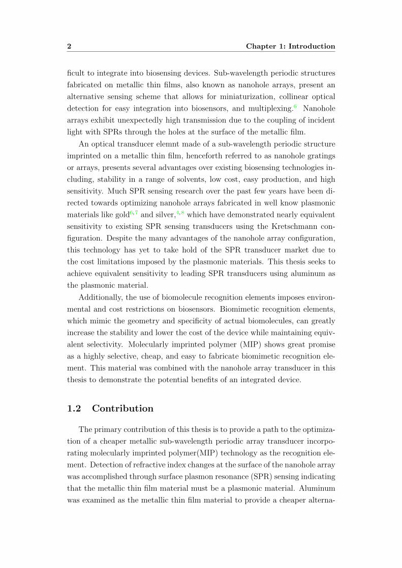
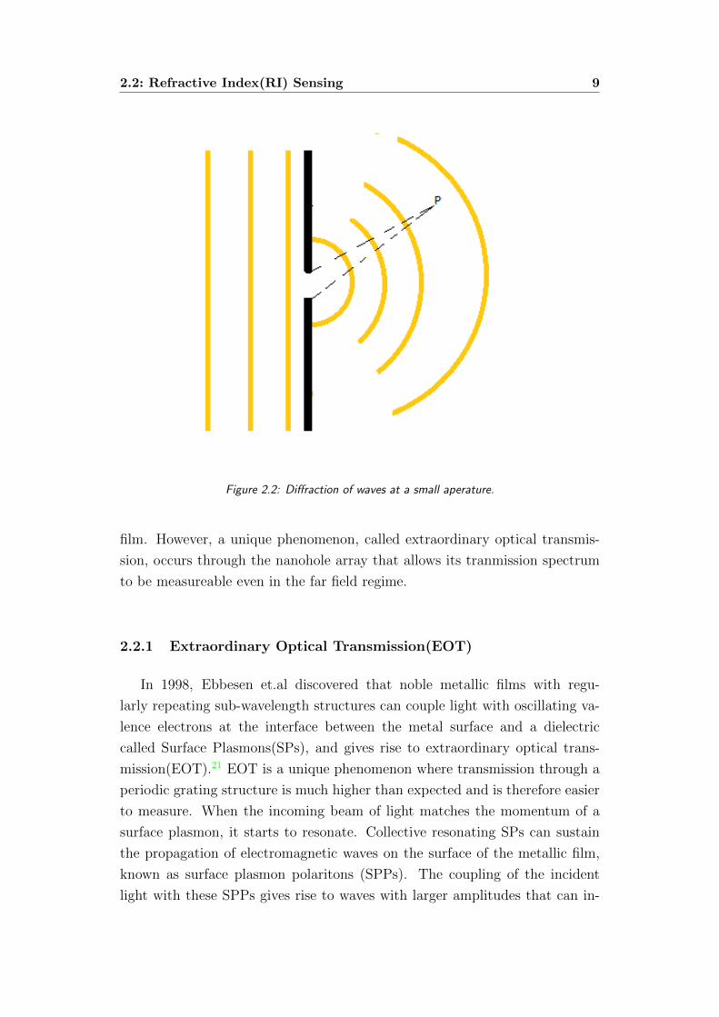
grating at normal incidence, as depicted in Figure 2.2.
Beyond the nanohole array, these nearly circular waves interfere either con-
structively when they are in-phase or destructively when they are out-of-phase
with each other. These additive and destructive components translate to peaks
and valleys in the intensity of diffracted light vs. wavelength graph, which is
also known as a transmission spectrum. Classical physics would predict that
the transmission would be very weak through the nanohole array and thus dif-
ficult to detect due to the size of the holes and opaqueness of the metallic thin
2.2: Refractive Index(RI) Sensing 9
Figure 2.2: Diffraction of waves at a small aperature.
film. However, a unique phenomenon, called extraordinary optical transmis-
sion, occurs through the nanohole array that allows its tranmission spectrum
to be measureable even in the far field regime.
2.2.1 Extraordinary Optical Transmission(EOT)
In 1998, Ebbesen et.al discovered that noble metallic films with regu-
larly repeating sub-wavelength structures can couple light with oscillating va-
lence electrons at the interface between the metal surface and a dielectric
called Surface Plasmons(SPs), and gives rise to extraordinary optical trans-
mission(EOT).21 EOT is a unique phenomenon where transmission through a
periodic grating structure is much higher than expected and is therefore easier
to measure. When the incoming beam of light matches the momentum of a
surface plasmon, it starts to resonate. Collective resonating SPs can sustain
the propagation of electromagnetic waves on the surface of the metallic film,
known as surface plasmon polaritons (SPPs). The coupling of the incident
light with these SPPs gives rise to waves with larger amplitudes that can in-

10 Chapter 2: Biosensing with Nanohole Arrays
terfere constructively or destructively to give enhanced transmission peaks and
dips that can be measured even in the far field regime.22
2.2.2 Transmission Spectroscopy
Transmission spectroscopy studies the dispersion of electromagnetic radia-
tion by matter through the measurement of intensity of transmitted light as
a function of wavelength. This principle was used to detect changes in RI at
the interface between the metallic surface of the nanohole array samples and
dielectric medium. Because the RI of the surrounding medium has an effect
on the momentum of light hitting the surface, it will change which SPs are
resonating and therefore which SPPs will propagate along the boundary be-
tween the metallic surface and dielectric medium. Furthermore, the SPP that
propagates along the metal-dielectric interface extends into each medium, so
the characteristics of this wave depend on the material conditions near the
interface. Hence, changes in RI along the interface have large effects on the
transmission spectrum. The binding of analytes to the recognition element
placed on top of the nanohole array changes the RI and therefore produces a
shift in the transmission peaks.
2.3 Factors Effecting RI Sensing
There are several factors that effect light transmission through a nanohole
array, including Rayleigh anomalies, Surface Plasmon Polariton-Bloch Waves,
and Rayleigh Anomaly-Surface Plasmon Polaritons. These spectral features
can exist on the top or bottom of the grating where it is touching a dielectric
medium. The coupling of two of these features will lead to a large constructive
or destructive interference, which will give rise to the peaks and dips in the
transmission spectrum. Any change in the RI at the surface of the grating
caused by a change in the dielectric medium adjacent to the metallic grating
will directly effect these spectral features. Therefore it is possible to predict the
position of peaks and dips in a spectrum once the spectral feature responsible
for each tranmission peak or dip is identified.
2.3.1 Rayleigh Anomalies(RAs)
Rayleigh anomalies(RAs) are non resonant spectral features associated with
the gratings that arise from the abrupt redistribution of energy when light is
2.3: Factors Effecting RI Sensing 11
diffracted at an angle parallel to the surface. They are sometimes called thresh-
old anomalies because they occur at the point where a diffracted order changes
from propagating at a angle less than 90◦to an evanescent wave propagating
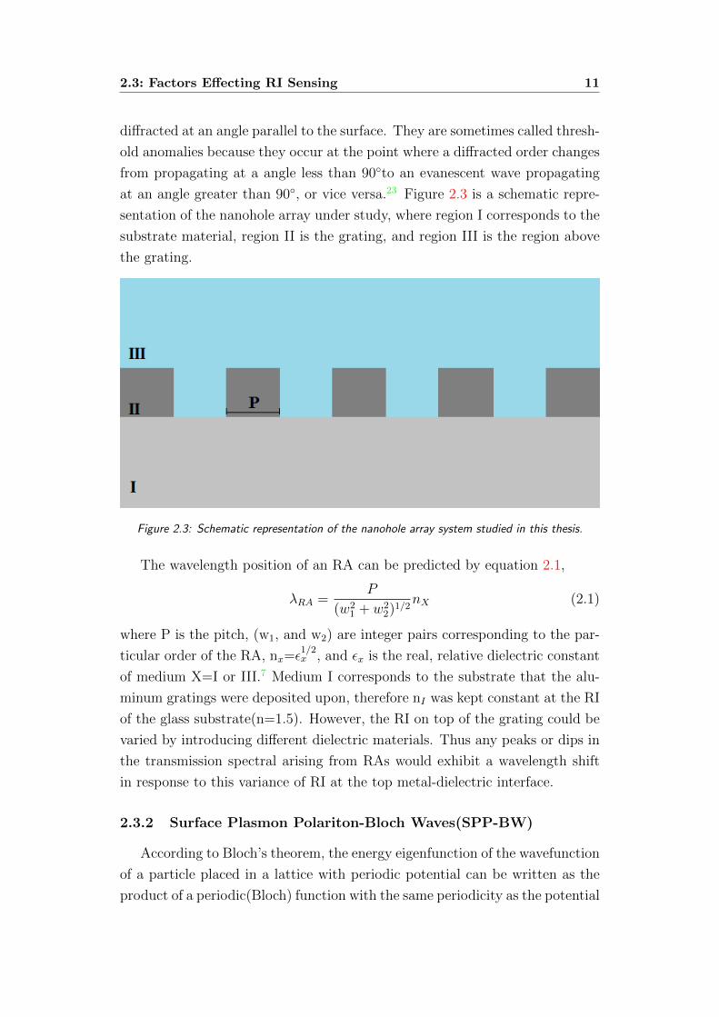
at an angle greater than 90◦, or vice versa.23 Figure 2.3 is a schematic repre-
sentation of the nanohole array under study, where region I corresponds to the
substrate material, region II is the grating, and region III is the region above
the grating.
Figure 2.3: Schematic representation of the nanohole array system studied in this thesis.
The wavelength position of an RA can be predicted by equation 2.1,
λRA =P
(w21 + w2
2)1/2nX (2.1)
where P is the pitch, (w1, and w2) are integer pairs corresponding to the par-
ticular order of the RA, nx=ε1/2x , and εx is the real, relative dielectric constant
of medium X=I or III.7 Medium I corresponds to the substrate that the alu-
minum gratings were deposited upon, therefore nI was kept constant at the RI
of the glass substrate(n=1.5). However, the RI on top of the grating could be
varied by introducing different dielectric materials. Thus any peaks or dips in
the transmission spectral arising from RAs would exhibit a wavelength shift
in response to this variance of RI at the top metal-dielectric interface.
2.3.2 Surface Plasmon Polariton-Bloch Waves(SPP-BW)
According to Bloch’s theorem, the energy eigenfunction of the wavefunction
of a particle placed in a lattice with periodic potential can be written as the
product of a periodic(Bloch) function with the same periodicity as the potential
12 Chapter 2: Biosensing with Nanohole Arrays
and a plane wave envelope.24 This wavefunction is a Bloch wave and can couple
with an SPP of the same resonance to create a surface plasmon polarition-bloch
wave(SPP-BW).
Because the metal nanoholes in Figure 2.3 are sandwiched between two
different dielectrics, SPP-BWs excited at the interface between region III and
II can tunnel through the nanoholes to the interface between region I and II,
where they are scattered back into plane waves that contribute to transmis-
sion.25 An n approximation for the free-space incident wavelength that can
excite an SPP-BW is
λSPP =P
(s21 + s2
2)1/2Re
(εAl(λSPP )εX)
εAl(λSPP ) + εX
)1/2
(2.2)
Where (s1, and s2) are integer pairs corresponding to the particular order of
the SPP-BW, P is the pitch,εAl(λSPP ) is the wavelength dependent relative
permittivity of aluminum, nx=ε1/2x , and εx is the real, relative dielectric con-
stant of medium X=I or III.7 This equation can be used predict the position
of SPP-BW waves through a nanohole array.
2.3.3 Rayleigh Anomaly-Surface Plasmon Polaritons(RA-SPPs)
The Rayleigh Anomaly-Surface Plasmon Polaritons(RA-SPP) effect occurs
when an SPP-BW from one side of the metallic thin film is coupled with a
RA on the other side, leading to a large increase in intensity of a narrow
transmission peak over a small RI range. A simple relation can be obtained by
equating the first order SPP-BW condition, (s1, and s2)=(1,0), on the region
I substrate(nI) with the first order RA condition,(w1, and w2)=(1,0), on the
region III substrate(n3), which is given in equation 2.3.
nIII = Re
(εAl(λRA−SPP )εIεAl(λRA−SPP ) + εI
)1/2
(2.3)
where λRA−SPP is the wavelength where the zero order SPP-BW and RA
conditions are the same. This equation demonstrates the dependence of the
RA-SPP wavelength on the RI. Any peak or dip originating from an RA-SPP
in the transmission spectrum of a grating will therefore be affected by a RI
change at the metal-dielectric interface. The relation between the periodicity
of the grating and λRA−SPP simplifies to equation 2.4, which means the bulk
sensitivity of a peak originating from an RA-SPP(dn/dλ) simply becomes the
periodicity of the grating.7
λRA−SPP = P × nIII (2.4)

2.4: Chapter Summary 13
2.4 Chapter Summary
In this chapter the principles supporting the use of RI sensing by nanohole
arrays as a transduction technique were introduced, beginning with the basic
principles of biosensing. The methods of classifying biosensors was discussed,
recognition and transduction elements were introduced, and label-based and
label-free methods of detection were compared. After an exploration of basic
RI sensing principles, including RI and diffraction, the specific phenomena
responsible for the ability of the nanohole array to act as a RI sensor were
discussed. The spectral features responsible for transmission peaks and dips
were then introduced. The next chapter provides insight into the materials and
methods used to fabricate and characterize the nanohole arrays as RI sensors
and introduces the characterization equipment used during experimentation.

14 Chapter 2: Biosensing with Nanohole Arrays

Chapter 3
Materials and Methods of
Characterization
3.1 Nanohole gratings fabricated on metallic substrates
The last chapter provided the theoretical basis for a nanohole array trans-
duction device, but it is necessary to quantify these claim by characterizing the
device. Nanohole gratings with 1 µm and 500 nm pitches imprinted on metallic
substrates were characterized as potential transducer components of RI sensors
by several methods including bulk sensitivity and thickness sensitivity. The
materials involved in the fabrication of the nanohole arrays and characteriza-
tion experiments are introduced in this chapter, and the procedures used to
characterize the device are described. Traditional and synthetic recognition
elements were attached to the surface to evaluate the operation of the inte-
grated RI sensing device. The effect of light polarizatioon was also examined.
The characterization equipment used during all experiments is mentioned and
the operation of th device is elucidated.
3.1.1 Fabrication of gratings
The nanohole grating structures analyzed during this project were fab-
ricated at the Instituto de Sistemas Optoelectrnicos y Microtecnologa, Uni-
versidad Politcnica de Madrid (ISOM-UPM). First, an aluminum layer was
deposited onto a previously washed 200 µm glass substrate by technicians at
UPM ISOM using a Varian VT 118 Electron Beam Physical Vapor Deposition
(EBPVD) machine. This process occurs under high vacuum where an electron
beam generated by a charged tungsten filament bombards an alumina anode
16 Chapter 3: Materials and Methods of Characterization
causing atoms of aluminum to transform into the gaseous phase. When evap-
orated, alumina dissociates into aluminum, AlO3, and Al2O. The aluminum
atoms then precipitate into solid form and form an even coating on top of
the glass substrate.26 The deposition rate was carefully controlled, leading to
a fairly even film thickness of 100-130nm. Aluminum was used as the grat-
ing material due to its low cost, compatibility with available fabrication and
characterization machinery, and ready availability.
A nanohole grating pattern is determined based on the desired pitch of the
RI device. The separation of the nanoholes is comparable to the desired pitch
of the grating. A nanohole grating pattern template was formed on top of the
aluminum layer using a nanolithography process. A ZEP520 positive resist
layer was spin coated on top of the aluminum layer using a Coater CONVAC
1001 spin coating system at 5000rpm for two minutes. The sample was then
baked for two minutes at 190◦C to remove the solvent, improve resist adhesion
to the substrate, and prevent bubbling during etching.
The nanoholes were then imprinted into the resist using a CRESTEC
CABL-9500C high resolution electron beam nanolithography system. The
machine was programmed to print the holes in a square grating pattern of
specified pitch that was repeated multiple times to get the proper length and
height of the desired grating. After the nanolithography process was complete,
the resist was developed by a ZED-N50 commercial developer for the employed
resist. Finally, the nanohole grating pattern was transferred to the aluminum
through an inductively coupled plasma(ICP)chemical etching process. The re-
maining resist was removed by soaking the nanohole array system in a 60◦C
1-methyl-2-pyrrolidone bath for ten minutes, and thoroughly washing the de-
vice in deionized water.
The resulting gratings were viewed under a scanning electron microscope
(SEM) to determine the extent of the etching process and the size and shape
of the holes. The SEM image of the 1µm grating, shown in Figure 3.1, has a
pitch of 0.970µ, which is very close to the intended pitch. It is important to
note that the size and shape of the holes are not identical to one another in
these gratings, which has an effect on the transmission spectrum. The 500nm
grating, shown in the SEM image of Figure 3.2, has a pitch of 496nm, which
is the closest achieved to that intended. It is easy to see the variation in the
size and shape of the holes in this image due to the close spacing of the holes.
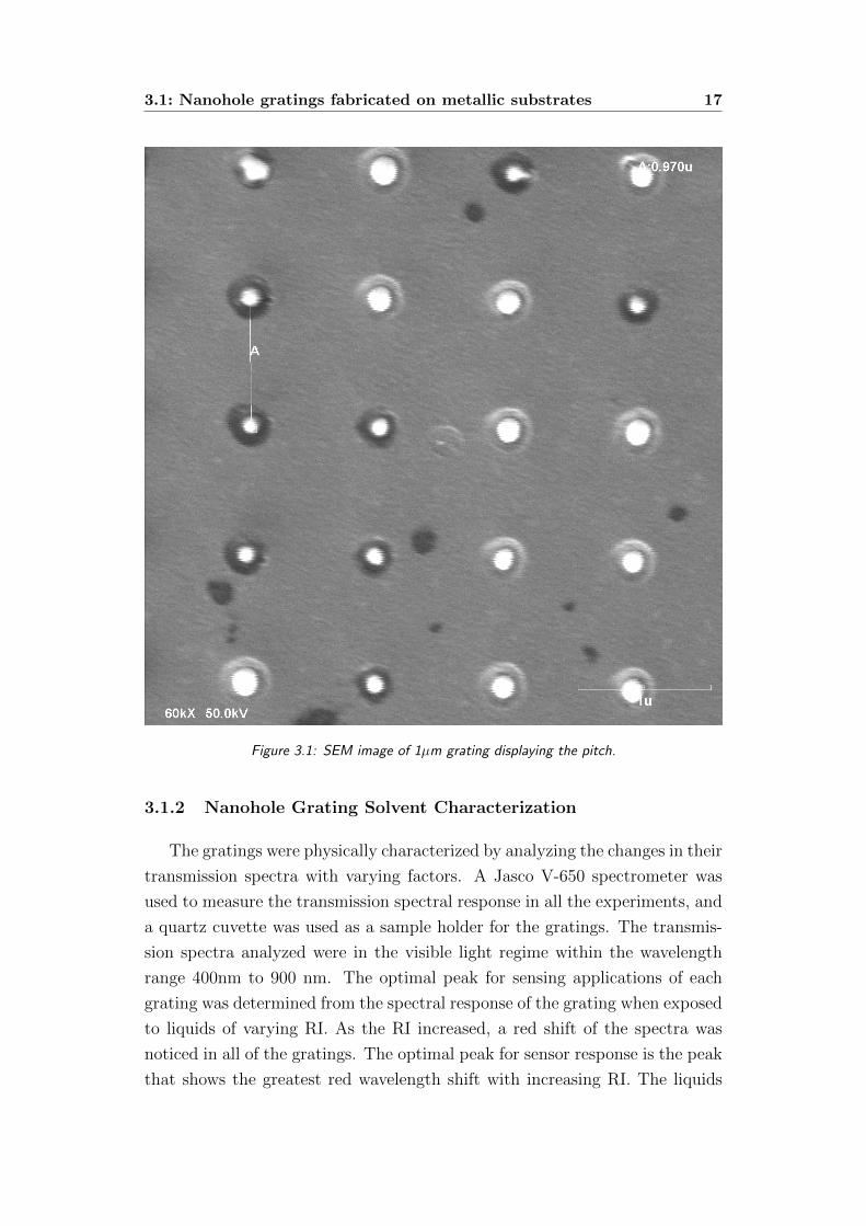
3.1: Nanohole gratings fabricated on metallic substrates 17
Figure 3.1: SEM image of 1µm grating displaying the pitch.
3.1.2 Nanohole Grating Solvent Characterization
The gratings were physically characterized by analyzing the changes in their
transmission spectra with varying factors. A Jasco V-650 spectrometer was
used to measure the transmission spectral response in all the experiments, and
a quartz cuvette was used as a sample holder for the gratings. The transmis-
sion spectra analyzed were in the visible light regime within the wavelength
range 400nm to 900 nm. The optimal peak for sensing applications of each
grating was determined from the spectral response of the grating when exposed
to liquids of varying RI. As the RI increased, a red shift of the spectra was
noticed in all of the gratings. The optimal peak for sensor response is the peak
that shows the greatest red wavelength shift with increasing RI. The liquids

18 Chapter 3: Materials and Methods of Characterization
Figure 3.2: SEM image of 500nm grating displaying the pitch.
used during the experiments were methanol, ethanol, isopropanol(IPA), cy-
clohexane, tetrahydrofuran(THF) and toluene. The refractive indices of these
liquids are given in Table 3.1. Matlab was used to process the transmission
data and determine the position of the peaks in the spectrum.
The bulk sensitivity, Sλ, is determined by the spectral change of the grat-
ing in response to varying RI (dn/dλ).27 The higher the spectrum shift with
changing RI, the more sensitive the device will be. The same liquids, shown
in Table 3.1 as those used to determine the optimal peak for sensing applica-
tions were used in the bulk sensitivity experiments. The measurements were
performed at room temperature(23◦C±4◦C).
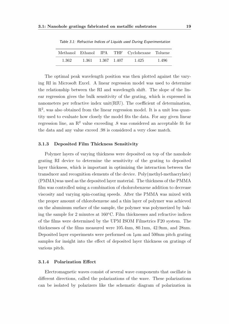
3.1: Nanohole gratings fabricated on metallic substrates 19
Table 3.1: Refractive Indices of Liquids used During Experimentation
Methanol Ethanol IPA THF Cyclohexane Toluene
1.362 1.361 1.367 1.407 1.425 1.496
The optimal peak wavelength position was then plotted against the vary-
ing RI in Microsoft Excel. A linear regression model was used to determine
the relationship between the RI and wavelength shift. The slope of the lin-
ear regression gives the bulk sensitivity of the grating, which is expressed in
nanometers per refractive index unit(RIU). The coefficient of determination,
R2, was also obtained from the linear regression model. It is a unit less quan-
tity used to evaluate how closely the model fits the data. For any given linear
regression line, an R2 value exceeding .8 was considered an acceptable fit for
the data and any value exceed .98 is considered a very close match.
3.1.3 Deposited Film Thickness Sensitivity
Polymer layers of varying thickness were deposited on top of the nanohole
grating RI device to determine the sensitivity of the grating to deposited
layer thickness, which is important in optimizing the interaction between the
transducer and recognition elements of the device. Poly(methyl-methacrylate)
(PMMA)was used as the deposited layer material. The thickness of the PMMA
film was controlled using a combination of cholorobenzene addition to decrease
viscosity and varying spin-coating speeds. After the PMMA was mixed with
the proper amount of chlorobenzene and a thin layer of polymer was achieved
on the aluminum surface of the sample, the polymer was polymerized by bak-
ing the sample for 2 minutes at 160◦C. Film thicknesses and refractive indices
of the films were determined by the UPM ISOM Filmetrics F20 system. The
thicknesses of the films measured were 105.4nm, 80.1nm, 42.9nm, and 28nm.
Deposited layer experiments were performed on 1µm and 500nm pitch grating
samples for insight into the effect of deposited layer thickness on gratings of
various pitch.
3.1.4 Polarization Effect
Electromagnetic waves consist of several wave components that oscillate in
different directions, called the polarizations of the wave. These polarizations
can be isolated by polarizers like the schematic diagram of polarization in

20 Chapter 3: Materials and Methods of Characterization
Figure 3.3. It is possible to optimize the coupling strength between incident
light and SPPs by adjusting the incident light polarization.28 The effect of
polarization on the transmission through the nanohole array was examined
by adding a polarizer in front of the light beam before it hit the sample and
blocking various polarizations of light, including, 0◦, 45◦, 90◦, and 180◦.
Figure 3.3: Demonstration of polarized light
3.2 Biomolecule Recognition Element
Biomolecule recognition elements in biosensors are natural receptors such as
antibodies, enzymes or cyclic sugars.29 The surface of the transducer element
in the biosensor is functionalized by these molecules to detect analytes in a
solution. Biomolecules are immobilized on the surface of the transducer and
then perform their normal functions. For example, an antibody will bind to a
viral strand. This natural selectivity identifies the presence or concentration
of an analyte that the transducer can then translate into a readable output.
In order to attach the biomolecule to the surface, the surface must first be
functionalized.

3.2: Biomolecule Recognition Element 21
3.2.1 Surface Functionalization
The functionalization of the surface of the nanohole grating patterned alu-
minum samples determines the ability of the sample to interact with its en-
vironment and selectively immobilize specific analytes on the transducer sur-
face.30 In this case, microcystin-leucine-arginine (MCLR), a very common
and potent cyanotoxin found in water that is capable of producing a number
of harmful side effects in humans and animals, was used for the biomolecu-
lar recognition experiments. First, the aluminum surface of the sample must
be modified with organofunctional silanes to provide suitable attachment sites
on the surface for covalent bonding of the MCLR to occur. An aminopropy-
ltriethoxysilane, which has a terminal amine group, was used as the silane
because of the availability of an amine reactive group on the MCLR. Follow-
ing the procedure of the liquid phase method of silization, the sample was
cleaned thoroughly and then immersed in a silane solution. Once the surface
was silanized, the MCLR was covalently bonded to available amide groups
on the surface. The MCLR was immobilized on the surface and ready to se-
lectively detect MCLR antibodies in water samples. The complete procedure
used to functionalize the biomolecule on the aluminum surface of the sample
is the same as that outlined by S. Herranz et.al. The functionalization of the
nanohole grating imprinted metallic films was performed by S. Herranz at the
Universidad Complutense de Madrid.31
3.2.2 Detection Protocol
The general procedure for biomolecule recognition involves exposing the
samples with immobilized MCLR on the surface to water samples containing
MCLR antibodies. The immobilized MCLR biomolecules on the surface will
bind to the MCLR antibodies contained in the water samples which should
register an effect in the transmission spectra of those samples. The exposure of
the samples containing immobilized MCLR on the surface was performed using
the protocol outlined S. Herranz et. al.31 Transmission spectra measurements
were taken by a spectrophotometer.
22 Chapter 3: Materials and Methods of Characterization
3.3 Molecularly Imprinted Polymer(MIP) Recognition
Element
MIP is created by a templating process at the molecular level. During this
process, the polymer is developed around a molecule, which is then extracted,
leaving corresponding imprints behind. The MIP is then able to bind targeted
molecules in a solution with similar shape and specificity, making MIPs highly
selective.11 This process can be applied to many different organic and inorganic
molecules, which makes MIP technology extremely versatile and widely appli-
cable, especially as the recognition element in biosensors. Synthetic recognition
elements like MIP remove many of the limitations that biomolecule recognition
elements impose on biosensing technologies, making the technology cheaper
and more applicable in a variety of situations. MIP in particular has selectiv-
ity comparable to traditional biomolecules with the added advantages of being
capable of producing receptors for a variety of molecular structures, enabling
large-scale chip fabrication, and offering superior stability when exposed to
solvents and temperature extremes.32
3.3.1 Fabrication
During the MIP formation process, functional monomers are assembled
around a specified target molecule and then fixed by crosslinking around the
target molecule during polymerization. The functional monomers are held to-
gether by either noncovalent (Figure 3.4(a)) or covalent forces (Figure 3.4(b)),
including electrostatic, hydrogen bonding and hydrophobic interactions. Co-
valent imprinting produces a higher yield of imprinting sites and is more ef-
ficient, but noncovalent imprinting allows a wider range of monomers, target
molecules, and imprinted materials.33 After polymerization has finished, the
template is removed by extraction with solvents/ hydrolysis for noncovalent
imprinting, or by chemical cleaving from the polymer for covalent imprinting,
which leaves behind sites similar in size and shape to the template molecule.
A methacrylate based novel polymer was used to make the MIP layer dur-
ing experimentation. This polymer was mixed with 30µg/mL of 6-amino-9-(2-
methoxycarbonylphenyl)[xanthen-3-ylidene]azanium chloride (Rhodamine 123),
which was the template molecule that was used to demonstrate the MIP’s se-
lective binding ability during experiments. Rhodamine 123 was chosen due to
its green fluorescence which is easily detectable by a fluorescent microscope.

3.3: Molecularly Imprinted Polymer(MIP) Recognition Element 23
Figure 3.4: Schematic overview of the (a) noncovalent and (b) covalent molecular imprinting
techniques
The polymer containing molecules of Rhodamine 123 was spin-coated on top
of the aluminum layer of the sample imprinted with a nanohole grating. After
an even layer of polymer mixture is distributed on the sample, a region of the
polymer mixture was defined over the grating structure of the sample using
a photolithography process. After exposure, the sample was developed with
THF to remove any unwanted polymer mixture from the regions surrounding
the grating structure. The remaining polymer mixture was crosslinked around
the Rhodamine 123 molecules through heating at 175◦Cfor one hour. At the
same time, a reference sample of non-imprinted polymer(NIP) was created in
a similar fashion on a separate sample with the same nanohole grating pitch.
However, the polymer did not contain Rhodamine 123 molecules so the final
film was just a layer of the polymerized polymer. The now crosslinked polymer
surrounding the Rhodamine 123 template molecules was washed in Methanol
three times for one hour each time in order to remove the template molecules.
This process leaves behind the molecular imprints in the polymer which can
now be used as a recognition element. Fluorescent microscopy was used to
ensure the complete removal of the Rhodamine 123 template molecules from
the crosslinked polymer.
3.3.2 Detection Protocol
Before incubation, the transmission spectra of the MIP covered nanohole
grating sample and the NIP reference sample were taken using a spectropho-
tometer. The nanohole grating imprinted metallic sample with MIP layer was
then incubated in a solution of 4ml hydrogen cyanide(HCN) with 30µg/mL
24 Chapter 3: Materials and Methods of Characterization
of Rhodamine 123 for a total of 18 hours. The sample was then dipped in
Methanol and dried with Nitrogen gas to prevent incubation solution build
up at the surface from affecting the measurements. The transmission spectra
and fluorescent images of both the MIP and NIP covered samples were taken
to determine if there was any recognition by the MIP and how effective the
nanohole grating imprinted metallic films were at detecting this recognition.
3.4 Characterization Equipment
The experimental methods discussed above use various equipment, includ-
ing a spectrophotometer, a flourescent microscope, and a film analyzer for
characterization of the nanohole array. This section explains the operation
of this equipment and how it was used to evaluate the performance of the
nanohole gratings as transduction elements. The spectrometer was used to
measure changes in the transmission spectrum of the nanohole array in re-
sponse to varying factors, such as different dielectric media on the top of the
nanohole array. The flourescent microscope was used to confirm the pres-
ence of target analyte during the MIP recognition experiments, while the film
analyzer determined the RI and thickness of deposited layers. The spectropho-
tometer, which measures light intensity as a function of wavelength, was the
most frequently used piece of equipment.
3.4.1 Spectrophotometer
In its simplest form a spectrophotometer consists of a white light source
and a detector placed on opposite sides of the sample being measured. As
light passes through the sample it diffractsand the intensity of light within the
detectors angular range is captured and translated by software into a read-
able output. This output is usually a graph of transmittance, absorption or
reflectance vs. wavelength of light.
A Jasco V-650 spectrometer belonging to UPM ISOM was used to make
the measurements of the transmission spectra through the nanohole grating
patterned samples. This research tool uses a light source with a broad range
of wavelengths from 400nm into the infrared range, although only wavelengths
in the visible range from 400nm to 850nm were used to achieve the transmis-
sion spectra. The spectrophotometer uses slightly more complicated optics to
focus the beam through the sample but generally works in the same way as

3.4: Characterization Equipment 25
described above. However, because the sample used had a nanohole grating
pattern on a semi-transparent aluminum film, much of the transmitted light
was greatly dispersed and the detector could not collect all of the transmitted
light. Therefore, an integrating sphere was used to focus all transmitted light
into the detector. Then the Jasco V-650 software was used to process the in-
formation and produce a graph of transmittance(%) vs. wavelength(nm), such
as the example spectrum of methanol shown in Figure 3.5.
Figure 3.5: Example of a transmission spectrum, Methanol reference in quartz cuvette
3.4.2 Fluorescent Microscope
Fluorescent microscopes irradiate a material with a high intensity beam of
light at a specific wavelength. Certain materials will then emit energy of a
much longer wavelength in the visible regime which is viewed as a magnified
image of the original sample. An Olimpus X51 confocal fluorescence micro-
scope with a 488 nm interferential filter and 600nm dichroic mirror was used
to perform flourescent microscopy of the samples. There was a cut-off in emis-
sion between camera and dichroic at 570 nm to avoid interferencial external
light. This technique was used to detect the presence of Rhodamine 123 dur-
26 Chapter 3: Materials and Methods of Characterization
ing the MIP recognition experiments because it appears fluorescent under the
microscope while the other materials in the sample do not.
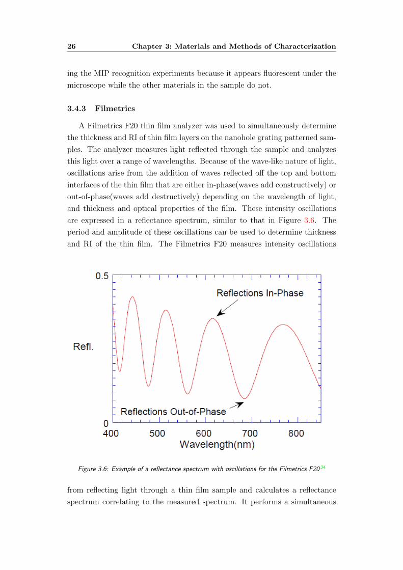
3.4.3 Filmetrics
A Filmetrics F20 thin film analyzer was used to simultaneously determine
the thickness and RI of thin film layers on the nanohole grating patterned sam-
ples. The analyzer measures light reflected through the sample and analyzes
this light over a range of wavelengths. Because of the wave-like nature of light,
oscillations arise from the addition of waves reflected off the top and bottom
interfaces of the thin film that are either in-phase(waves add constructively) or
out-of-phase(waves add destructively) depending on the wavelength of light,
and thickness and optical properties of the film. These intensity oscillations
are expressed in a reflectance spectrum, similar to that in Figure 3.6. The
period and amplitude of these oscillations can be used to determine thickness
and RI of the thin film. The Filmetrics F20 measures intensity oscillations
Figure 3.6: Example of a reflectance spectrum with oscillations for the Filmetrics F2034
from reflecting light through a thin film sample and calculates a reflectance
spectrum correlating to the measured spectrum. It performs a simultaneous

3.5: Chapter Summary 27
analysis of thickness and RI of the thin films by varying RI to optimize the
correlation between the calculated and measured reflectance spectra.
3.5 Chapter Summary
The materials used in the fabrication and characterization of the nanohole
array RI sensor were discussed in this section. The fabrication methods of the
nanohole array, biomolecule recognition element, and MIP recognition layer
were explained, as well as the methods of detection used to determine the abil-
ity of the nanohole array to act as a RI sensor. The basic operating principles
of the equipment used for characterization of the device was also discussed.
In the next chapter, the origins of the transmission spectra of the nanohole
gratings will be explored as well as the theoretical characterization and opti-
mization of the nanohole array as a RI sensor.

28 Chapter 3: Materials and Methods of Characterization
Chapter 4
Theoretical
In order to optimize the design of the nanohole grating RI sensing device
for biomolecule recognition, finite-difference time-domain(FDTD) simulations
were performed. Lumerical FDTD solutions were used to optimize the pitch
and thickness of nanohole grating patterned aluminum films. This software
uses the finite-difference time-domain(FDTD) method to solve Maxwell’s equa-
tions in 3D and is capable of analyzing the interaction of UV, visible, and IR
radiation with the sub-wavelength periodic structures imprinted in aluminum
films. The origins of the transmission spectra, including RAs, SPP-BWs, and
RA-SPPs, of the gratings characterized in this thesis are discussed here. The
nanohole grating has great potential to couple light into a waveguide, which is
also discussed.
4.1 Finite-Difference Time-Domain(FDTD) Simulations
The finite-difference time-domain(FDTD) method is a numerical analysis
technique that solves Maxwell’s equations for electric and magnetic field dis-
tributions in the time-domain. This technique enables it to simulate many
frequencies at one time in a discretized spatial domain in order to model the
interaction of the electromagnetic field with physical objects. The central
difference approximation is used to discretize the time-dependent Maxwell’s
equations in both the spatial and time domains.
The Maxwell-Faraday and Maxwell-Ampere laws are given by Equations
4.1 and 4.2, respectively,
5× ~E = −µ∂~H
∂t− σM ~H (4.1)
30 Chapter 4: Theoretical
5× ~H = ε∂ ~E
∂t− σ ~E (4.2)
where ~E is the electric field, ~H is the magnetic field, µ is the magnetic perme-
ability, ε is the dielectric permittivity, and σ is the electric conductivity. These
equations can also be expressed in the form of six directionally dependent field
equations in Cartesian coordinates that describe anisotropic materials by using
different values of dielectric parameters along the different directions.
The FDTD solution is reached by numerically solving the finite-difference
equations resulting from discretizing Maxwell’s equations in a leapfrog manner,
meaning that the electric and magnetic field vector components in a volume of
space are solved one after another at consecutive instants in time.35 This solu-
tion is second order accurate and stable if the time step satisfies the Courant
condition:
∆t ≤ 1
c√
1∆x2
+ 1∆y2
+ 1∆z2
(4.3)
where c is the speed of light, and ∆x, ∆y, ∆z are the time steps of the dis-
cretizations in the x-, y-, and z- directions, respectively.
The computational domain of the simulation is typically discretized using
a rectangular unit cell with the electric and magnetic vector field components
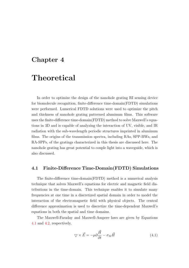
spatially staggered around the cube as proposed in Yee’s scheme, shown in
Figure 4.1.36 This domain must be established in any FDTD calculations as
it defines the region over which the simulations are performed and the electric
and magnetic fields are determined at every point inside this space.
4.1.1 Lumerical Software
Numerical analysis of the nanohole grating geometry was performed with
FDTD Solutions by Lumerical Solutions, Inc. This software is capable of
analyzing the interaction of UV, visible, and IR radiation with the nanohole
array structure,. However, only the spectrum from 400nm to 850nm was used
during simulations. The software follows the same general procedure described
above for determining the FDTD solution. The algorithm splits the discretized
Maxwell’s equations into two independent sets of equations composed of three
vector quantities that can only be solved in the x-y plane. The TE (transverse
electric) equations include the x and y components of the electric field and
the z component of the magnetic field, where as the TM (transverse magnetic)
4.1: Finite-Difference Time-Domain(FDTD) Simulations 31
Figure 4.1: Position of the field components in Yee’s cell. The electric field components are in
the middle of the edges and the magnetic field components are in the center of the faces such
that each electric(E) field vector component is located midway between a pair of magnetic(H)
field vector components, and vice versa.36
equations include the z electric field component and the x and y magnetic field
components.
The Lumerical software uses a rectangular Cartesian coordinate mesh as the
computational domain. At each mesh point, the electric and magnetic fields
are calculated. Using a smaller mesh gives a more accurate representation of
the device, but also increases the simulation time and memory requirements.37
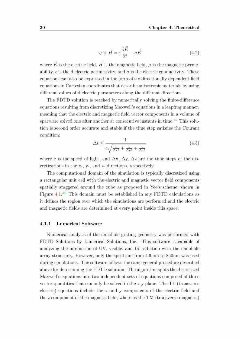
Because the grating was periodic, the FDTD region was composed of a single
unit cell shown in Figure 4.2. The radius and the thickness of the aluminum
layer were kept constant at 150 nm and 80 nm, respectively, which were their
average measured values during experimentation. The bottom dielectric, which
represents the glass substrate underneath the nanohole array fabricated in
aluminum, had a constant RI of 1.5, but the top dielectric was varied during
simulations. It was assumed during simulations that the nanoholes penetrated
the aluminum completely and reached the glass, although in actuality there
32 Chapter 4: Theoretical
would be a cone-like cavity instead of a perfectly cylindrical one due to errors
during fabrication.
Figure 4.2: Images from the Lumerical saoftware of (a)the FDTD region simulated where a is
the pitch of the grating and r is the radius of hole, (b) 3D view of the grating including upper
dielectric region, nanohole array, and lower dielectric substrate
Simulations were performed to compare with the experimental results of
the effect of varying solvents on nanohole arrays with 500nm and 1µm pitches.
All conditions of the nanohole array structure were kept constant except for
the RI of a simulated dielectric layer on top of the nanohole. Additionally,
the effect of deposited thick layer(200nm-1.5µm) and thin layer(30nm-100nm)
thicknesses on the transmission spectrum of the nanohole arrays was performed
on the two different pitched gratings. Again the RI of the simulated top layer
dielectric material was varied, but the RI did not vary as greatly with thickness
as with solvents. Thus, smaller RI changes of the dielectric were simulated. It
was assumed that thick layers completely filled the nanoholes, while thin layers
did not. Therefore, these were the conditions imposed in the simulations to
differentiate between thick and thin layers.
An optimization study of the pitch was also performed to determine the
optimal grating structure to use for the device. A maximum transmission
parameter, which represented the maximum transmission of the highest peak,
was created and the optimization swept across various pitches to maximize
this high transmission.
4.1: Finite-Difference Time-Domain(FDTD) Simulations 33
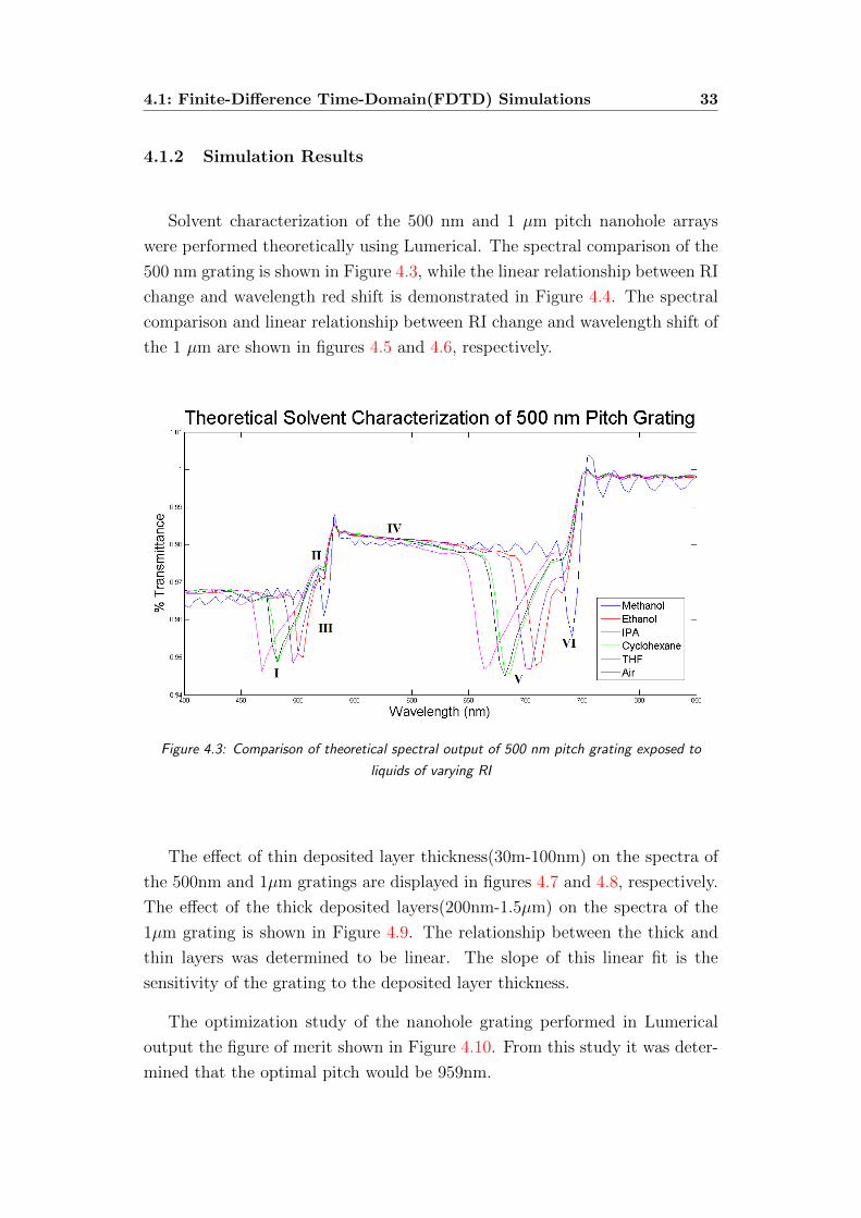
4.1.2 Simulation Results
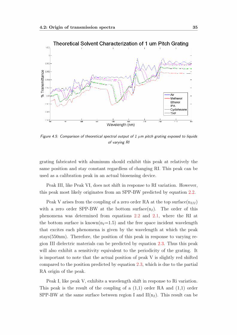
Solvent characterization of the 500 nm and 1 µm pitch nanohole arrays
were performed theoretically using Lumerical. The spectral comparison of the
500 nm grating is shown in Figure 4.3, while the linear relationship between RI
change and wavelength red shift is demonstrated in Figure 4.4. The spectral
comparison and linear relationship between RI change and wavelength shift of
the 1 µm are shown in figures 4.5 and 4.6, respectively.
Figure 4.3: Comparison of theoretical spectral output of 500 nm pitch grating exposed to
liquids of varying RI
The effect of thin deposited layer thickness(30m-100nm) on the spectra of
the 500nm and 1µm gratings are displayed in figures 4.7 and 4.8, respectively.
The effect of the thick deposited layers(200nm-1.5µm) on the spectra of the
1µm grating is shown in Figure 4.9. The relationship between the thick and
thin layers was determined to be linear. The slope of this linear fit is the
sensitivity of the grating to the deposited layer thickness.
The optimization study of the nanohole grating performed in Lumerical
output the figure of merit shown in Figure 4.10. From this study it was deter-
mined that the optimal pitch would be 959nm.

34 Chapter 4: Theoretical
Figure 4.4: Determination of theoretical bulk sensitivity for 500 nm pitch grating
4.2 Origin of transmission spectra
The transmission spectral output of the nanohole arrays is dependent on
many factors, and is therefore not straightforward. Figures 4.5 and 4.3 show
the theoretical output spectra of the 1µm and 500nm pitch, respectively, in
response to different solvents with varying refractive indices. The 500nm pitch
grating will be used to discuss the origins of spectral features. However, the
1µm pitch is used to support some of the claims made for the origin of spec-
tral features for the 500 nm grating. Each of the peaks in the 500 nm pitch
transmission spectrum are classified by a roman numeral, which is how each
peak will be referred to throughout this discussion.
The spectra of both the 1µm and 500nm pitch gratings exhibit a slight drop
in transmission around 750nm(peak VI in the 500nm spectrum). According
to literature, aluminum, the metallic material the gratings are imprinted on,
has a well known absorption peak at 1.6eV due to conductivity.38 This photon
energy is related to the wavelength by equation 4.4,
E =hc
λ(4.4)
where h is Plank’s constant(4.13566733×10⁻¹⁵eVs), c is the speed of light(299792458
m/s), E is the energy of the photon (eV), and λ is the wavelength (nm). Be-
cause the aluminum is blocking the transmission of 750nm wavelength, every
4.2: Origin of transmission spectra 35
Figure 4.5: Comparison of theoretical spectral output of 1 µm pitch grating exposed to liquids
of varying RI
grating fabricated with aluminum should exhibit this peak at relatively the
same position and stay constant regardless of changing RI. This peak can be
used as a calibration peak in an actual biosensing device.
Peak III, like Peak VI, does not shift in response to RI variation. However,
this peak most likely originates from an SPP-BW predicted by equation 2.2.
Peak V arises from the coupling of a zero order RA at the top surface(nIII)
with a zero order SPP-BW at the bottom surface(nI). The order of this
phenomena was determined from equations 2.2 and 2.1, where the RI at
the bottom surface is known(nI=1.5) and the free space incident wavelength
that excites each phenomena is given by the wavelength at which the peak
stays(550nm). Therefore, the position of this peak in response to varying re-
gion III dielectric materials can be predicted by equation 2.3. Thus this peak
will also exhibit a sensitivity equivalent to the periodicity of the grating. It
is important to note that the actual position of peak V is slightly red shifted
compared to the position predicted by equation 2.3, which is due to the partial
RA origin of the peak.
Peak I, like peak V, exhibits a wavelength shift in response to Ri variation.
This peak is the result of the coupling of a (1,1) order RA and (1,1) order
SPP-BW at the same surface between region I and II(nI). This result can be

36 Chapter 4: Theoretical
Figure 4.6: Determination of theoretical bulk sensitivity for 1 µm pitch grating
predicted by equations 2.2 and 2.1. Because these spectral features are first
order, the sensitivity will not be equivalent to the periodicity.
Peaks II and IV are simply regions of constructive interference where no
spectral features are causing a dip in transmission. Thus they are maxima
arising from the presence of minima in the spectrum and are related to the
general transmission through the nanoholes.
4.2.1 Hole Geometry
The geometry of the holes can have an effect on the position and transmis-
sion through the holes because any change in the holes will change the surface
plasmons that will be excited by incoming light. Moreno et.al examined the
sensitivity of the transmission spectrum to nonuniformities in the hole area
in order to explain minor inconsistencies between their theoretical and ex-
perimental results. They confirmed that changes in the geometry of the holes
accounted for the small variations in transmission efficiency and peak positions
between thier theoretical and experimental results.39
In another study, Koerkamp et.al observed the effect of hole shape on
the transmission spectra of nanohole arrays and found that using rectangular
shaped holes enhanced transmission and caused a red shift in the spectrum.40
In a later study, Molen et.al demonstrated that there are localized modes in-

4.3: Coupling Light into a waveguide 37
Figure 4.7: Theoretical deposited layer thickness effect(<100 nm) of the 500 nm pitch grating
side the rectangular holes arising from additional shape resonances that are
not present in circular holes. These localized modes effectively acted as waveg-
uides increasing the coupling efficiency of surface plasmons between both sides
of the film and gave rise to further enhanced transmission and slight red shifts
in the spectrm.41 Thus, irregularities in the size and shape of the holes can
effect the spectral output of the nanohole arrays.
4.3 Coupling Light into a waveguide
The RI mismatch between a high RI guiding layer surrounded by materials
with lower refractive indices in an optical waveguide causes total internal reflec-
tion(TIR) of light. When light is coupled into this guiding layer, the majority
of that light is successfully trapped inside the waveguide so that it can propa-
gate over long distances. However, some of the light extends into the substrate
and medium in the form of an electromagnetic wave, called the evanescent field,
which experiences an exponential decay in amplitude as it moves away from
the surface. The angle of incident light is changed to match the evanescent
wave propagation rate with the propagation rate of the SPPs.42 Thus the field
extends into the recognition substrate and sample medium thereby enhancing
the sensitivity of molecule recognition because of the large difference between
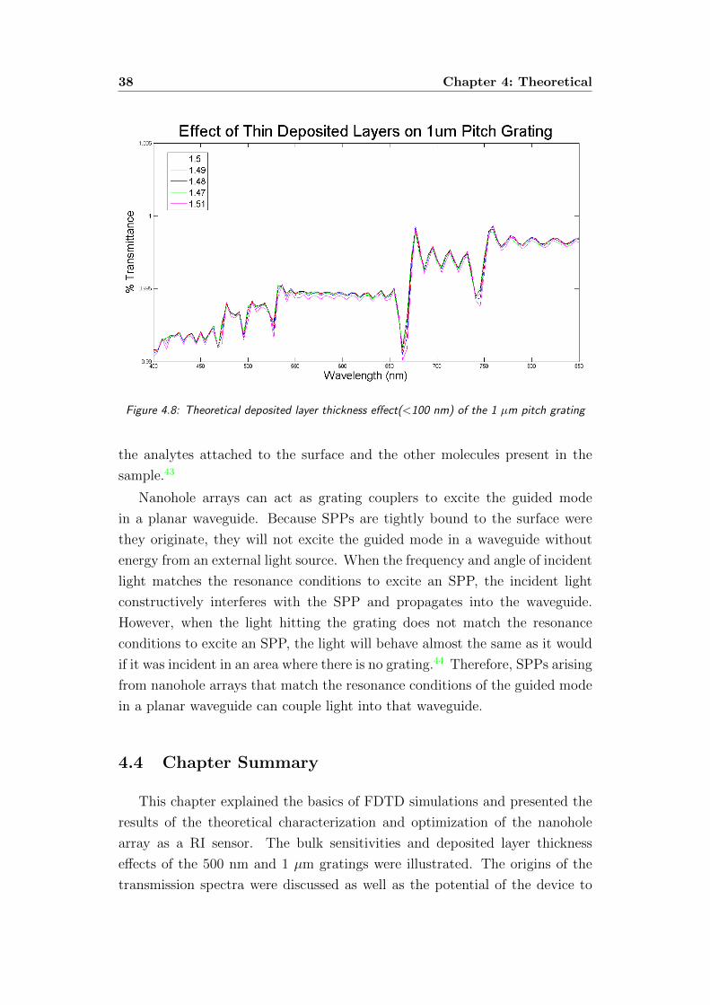
38 Chapter 4: Theoretical
Figure 4.8: Theoretical deposited layer thickness effect(<100 nm) of the 1 µm pitch grating
the analytes attached to the surface and the other molecules present in the
sample.43
Nanohole arrays can act as grating couplers to excite the guided mode
in a planar waveguide. Because SPPs are tightly bound to the surface were
they originate, they will not excite the guided mode in a waveguide without
energy from an external light source. When the frequency and angle of incident
light matches the resonance conditions to excite an SPP, the incident light
constructively interferes with the SPP and propagates into the waveguide.
However, when the light hitting the grating does not match the resonance
conditions to excite an SPP, the light will behave almost the same as it would
if it was incident in an area where there is no grating.44 Therefore, SPPs arising
from nanohole arrays that match the resonance conditions of the guided mode
in a planar waveguide can couple light into that waveguide.
4.4 Chapter Summary
This chapter explained the basics of FDTD simulations and presented the
results of the theoretical characterization and optimization of the nanohole
array as a RI sensor. The bulk sensitivities and deposited layer thickness
effects of the 500 nm and 1 µm gratings were illustrated. The origins of the
transmission spectra were discussed as well as the potential of the device to
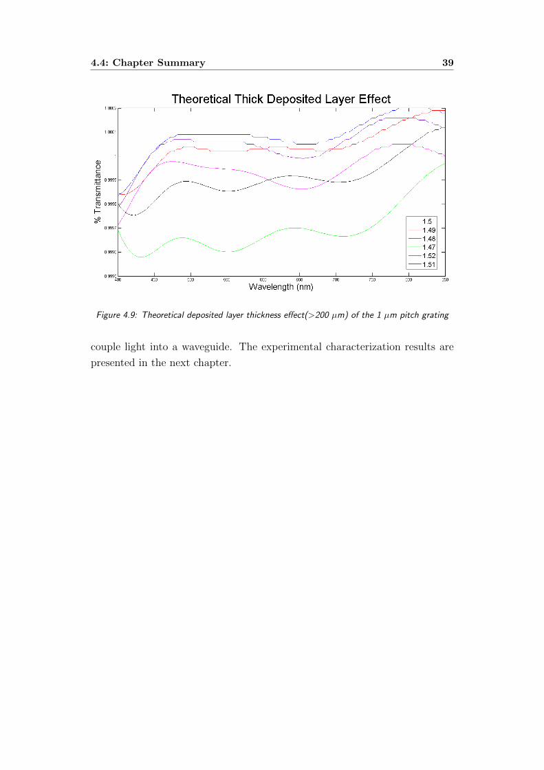
4.4: Chapter Summary 39
Figure 4.9: Theoretical deposited layer thickness effect(>200 µm) of the 1 µm pitch grating
couple light into a waveguide. The experimental characterization results are
presented in the next chapter.

40 Chapter 4: Theoretical
Figure 4.10: Figure of Merit from the Lumerical pitch optimization simulation which
demonstrates the pitch that gives the sharpest transmission spectrum.
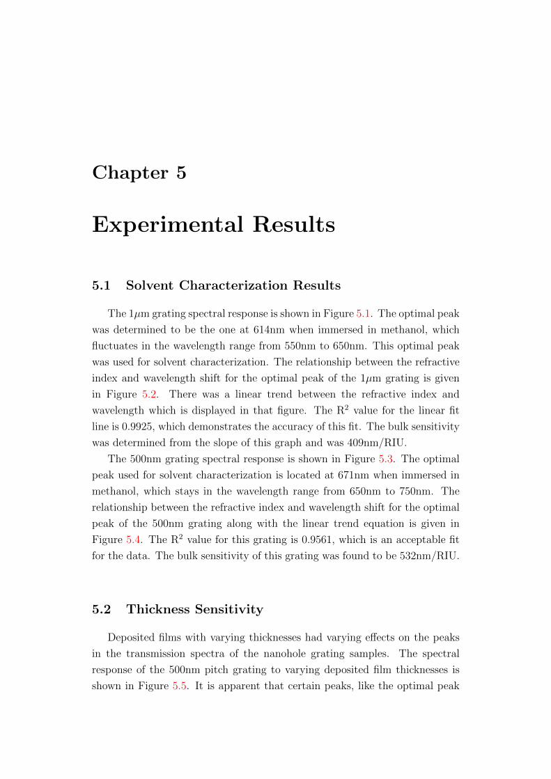
Chapter 5
Experimental Results
5.1 Solvent Characterization Results
The 1µm grating spectral response is shown in Figure 5.1. The optimal peak
was determined to be the one at 614nm when immersed in methanol, which
fluctuates in the wavelength range from 550nm to 650nm. This optimal peak
was used for solvent characterization. The relationship between the refractive
index and wavelength shift for the optimal peak of the 1µm grating is given
in Figure 5.2. There was a linear trend between the refractive index and
wavelength which is displayed in that figure. The R2 value for the linear fit
line is 0.9925, which demonstrates the accuracy of this fit. The bulk sensitivity
was determined from the slope of this graph and was 409nm/RIU.
The 500nm grating spectral response is shown in Figure 5.3. The optimal
peak used for solvent characterization is located at 671nm when immersed in
methanol, which stays in the wavelength range from 650nm to 750nm. The
relationship between the refractive index and wavelength shift for the optimal
peak of the 500nm grating along with the linear trend equation is given in
Figure 5.4. The R2 value for this grating is 0.9561, which is an acceptable fit
for the data. The bulk sensitivity of this grating was found to be 532nm/RIU.
5.2 Thickness Sensitivity
Deposited films with varying thicknesses had varying effects on the peaks
in the transmission spectra of the nanohole grating samples. The spectral
response of the 500nm pitch grating to varying deposited film thicknesses is
shown in Figure 5.5. It is apparent that certain peaks, like the optimal peak
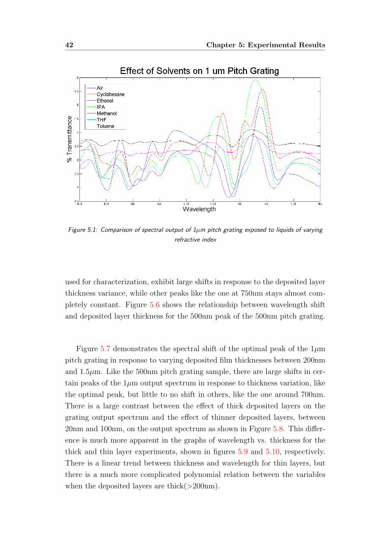
42 Chapter 5: Experimental Results
Figure 5.1: Comparison of spectral output of 1µm pitch grating exposed to liquids of varying
refractive index
used for characterization, exhibit large shifts in response to the deposited layer
thickness variance, while other peaks like the one at 750nm stays almost com-
pletely constant. Figure 5.6 shows the relationship between wavelength shift
and deposited layer thickness for the 500nm peak of the 500nm pitch grating.
Figure 5.7 demonstrates the spectral shift of the optimal peak of the 1µm
pitch grating in response to varying deposited film thicknesses between 200nm
and 1.5µm. Like the 500nm pitch grating sample, there are large shifts in cer-
tain peaks of the 1µm output spectrum in response to thickness variation, like
the optimal peak, but little to no shift in others, like the one around 700nm.
There is a large contrast between the effect of thick deposited layers on the
grating output spectrum and the effect of thinner deposited layers, between
20nm and 100nm, on the output spectrum as shown in Figure 5.8. This differ-
ence is much more apparent in the graphs of wavelength vs. thickness for the
thick and thin layer experiments, shown in figures 5.9 and 5.10, respectively.
There is a linear trend between thickness and wavelength for thin layers, but
there is a much more complicated polynomial relation between the variables
when the deposited layers are thick(>200nm).

5.3: Polarization 43
Figure 5.2: Determination of Bulk Sensitivity for 1µm pitch grating
5.3 Polarization
The effect of exposing the grating to different polarizations of light is shown
in Figure 5.11. There is some variation in transmission but not in the position
of the peaks.
5.4 Biomolecule detection
The effect of biomolecule recognition on the transmission spectrum of a
500nm pitch nanohole grating sample was very pronounced. Figure 5.12 demon-
strates the effect of each step of the functionalization and recognition processes
on the spectral output of the gratings. From this graph it was determined that
there was a 22nm wavelength shift towards the red part of the spectrum in
the peak around 550nm from the original nanohole array to the final sample
with recognized molecules on the top. However, there is only a 10nm red shift
of the spectrum in the peak around 550nm in response to MCLR antibodies
binding to the MCLR molecules immobilized on the surface of the samples.
Selective molecule recognition was confirmed at UPM ISOM by using the bare
glass comparison procedures explained by Herranz et.al.31
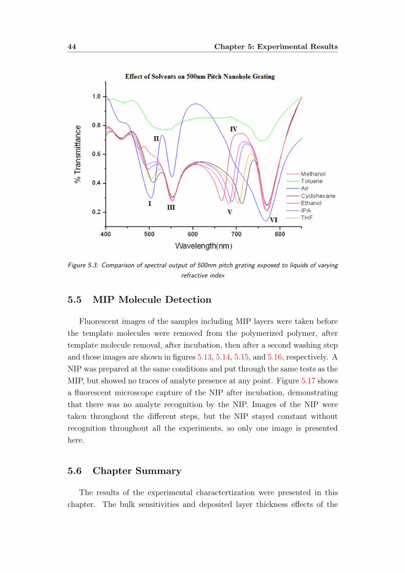
44 Chapter 5: Experimental Results
Figure 5.3: Comparison of spectral output of 500nm pitch grating exposed to liquids of varying
refractive index
5.5 MIP Molecule Detection
Fluorescent images of the samples including MIP layers were taken before
the template molecules were removed from the polymerized polymer, after
template molecule removal, after incubation, then after a second washing step
and those images are shown in figures 5.13, 5.14, 5.15, and 5.16, respectively. A
NIP was prepared at the same conditions and put through the same tests as the
MIP, but showed no traces of analyte presence at any point. Figure 5.17 shows
a fluorescent microscope capture of the NIP after incubation, demonstrating
that there was no analyte recognition by the NIP. Images of the NIP were
taken throughout the different steps, but the NIP stayed constant without
recognition throughout all the experiments, so only one image is presented
here.
5.6 Chapter Summary
The results of the experimental charactertization were presented in this
chapter. The bulk sensitivities and deposited layer thickness effects of the

5.6: Chapter Summary 45
Figure 5.4: Determination of Bulk Sensitivity for 500nm pitch grating
fabricated 500 nm and 1 µm pitch nanohole arrays were illustrated. The results
of the biomolecule and MIP recognition experiments were also displayed. The
significance of these results and comparsion to the theoretical results presented
in the last chapater will be discussed in the next chapter.

46 Chapter 5: Experimental Results
Figure 5.5: Effect of deposited layer thickness on the transmission spectrum of the 500nm
pitch nanohole grating sample for layer thicknesses smaller than 100 nm
Figure 5.6: Effect of deposited layer thickness on the transmission spectrum of the 500nm
pitch nanohole grating sample

5.6: Chapter Summary 47
Figure 5.7: Effect of deposited layer thickness, between 200nm and 1.5µm, on the output
spectrum of the 1µm pitch nanohole grating sample
Figure 5.8: Effect of deposited layer thickness, between 20nm and 100nm, on the output
spectrum of the 1µm pitch nanohole grating sample

48 Chapter 5: Experimental Results
Figure 5.9: Relationship between deposited layer thickness, between 200nm and 1.5µm, and
wavelength of the 1µm pitch nanohole grating sample
Figure 5.10: Relationship between deposited layer thickness, between 20nm and 100nm, and
wavelength of the 1µm pitch nanohole grating sample

5.6: Chapter Summary 49
Figure 5.11: Effect of polarizing incoming light on the transmission spectrum of the 500nm
grating.
Figure 5.12: Comparison of the transmission spectra of a 500nm pitch grating during the steps
of biomolecule recognition, which include functionalization of the metallic surface of the
sample, immobilization of MCLR molecules onto that surface, and attachment of MCLR
antibodies when exposed to an incubation solution
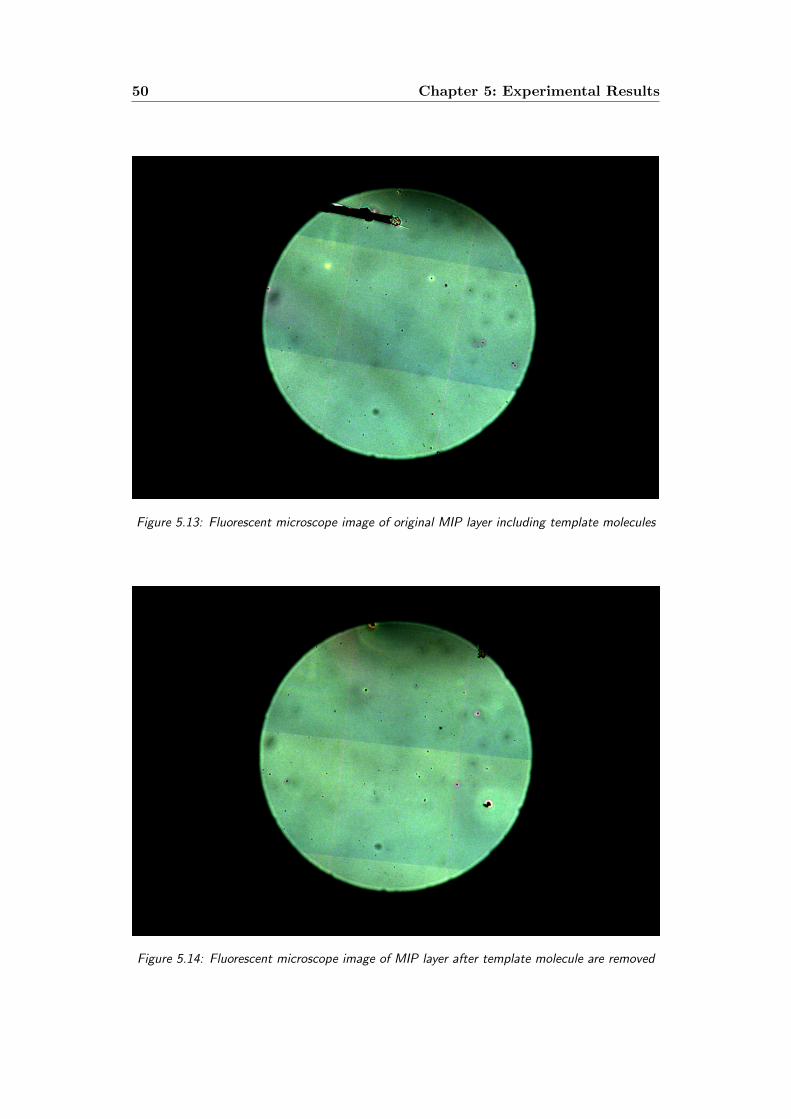
50 Chapter 5: Experimental Results
Figure 5.13: Fluorescent microscope image of original MIP layer including template molecules
Figure 5.14: Fluorescent microscope image of MIP layer after template molecule are removed
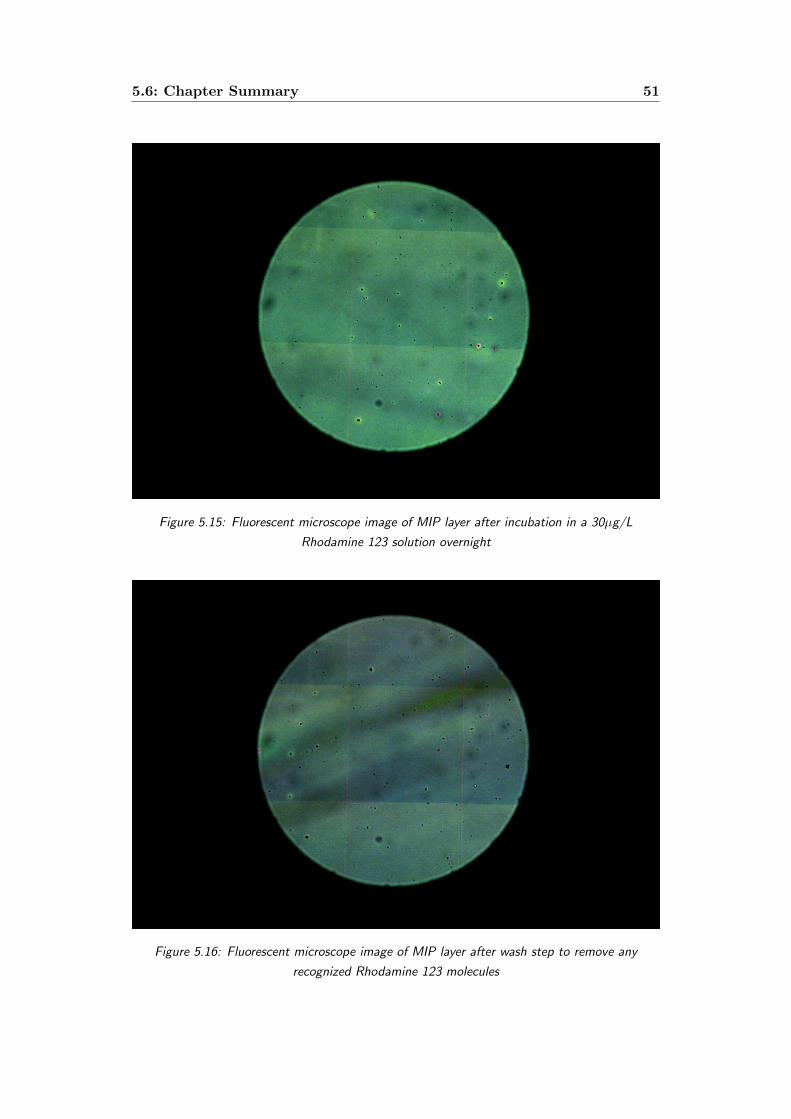
5.6: Chapter Summary 51
Figure 5.15: Fluorescent microscope image of MIP layer after incubation in a 30µg/L
Rhodamine 123 solution overnight
Figure 5.16: Fluorescent microscope image of MIP layer after wash step to remove any
recognized Rhodamine 123 molecules
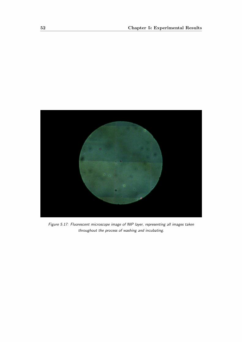
52 Chapter 5: Experimental Results
Figure 5.17: Fluorescent microscope image of NIP layer, representing all images taken
throughout the process of washing and incubating.

Chapter 6
Discussion
6.1 Solvent Characterization
The theoretical transmission spectrum responding to solvents with varying
refractive indices (Figure 4.3) had much sharper peaks than the experimental
spectral output(Figure 5.3) for the 500 nm pitch grating, which is the result of
variations in the geometry of the holes. The experimental output also had extra
peaks arising from additional interference between unexpected excitations of
surface plasmons, which most likely resulted from variations in the hole shape.
Figure 3.2 shows an SEM picture of the nanohole arrays in which it is noticed
that that some of the shapes are elliptical and start to resemble rectangular
structures. According to the theory, shape resonances may be arising from this
more rectangular shape which could give rise to the additional peaks in the
experimental spectrum. This could also be the reason that the bulk sensitivity
of the 500 nm experimental nanohole array (532 nm/RIU) was higher than
theoretical expectations (465 nm/RIU).
The nearly linear trend seen in the experimental and theoretical bulk sen-
sitivity determinations based on Peak I can be explained by equation 2.4. The
experimental and theoretically determined graphs of wavelength as functions
of surface refractive index variance is very similar to the zero order positions of
RAs as a function of RI variance in region III. Furthermore, the slopes of these
graphs, which represent the bulk sensitivity, were very close to the periodicity
of the grating (500 nm) because they are due to RA-SPP phenomenon. Peak
III can be explained in the same way, but the bulk sensitivity(315 nm/RIU)
calculated for this pitch is not as close to the pitch of the grating and has more
variation in the linear trend. These variations are most likely due to an inexact
matching of the RA and SPP-BW. Peak III is much broader than peak I and

54 Chapter 6: Discussion
does not occur when the region III medium is air or toluene, which suggests
that the incoming beam of light only matches the resonance of SPPs at this
wavelength in a limited RI range. Therefore this spectral feature was not used
as the characterization peak of the device for refractive index sensing.
The nanohole arrays imprinted in aluminum showed similar bulk sensi-
tivity(532 nm/RIU) to nanohole arrays imprinted in silver(450 nm/RIU) and
gold(500nm/RIU), despite these noble metals being a better-performance plas-
monic materials.4,7 These results have demonstrated that aluminum, a much
cheaper metal, can replace more expensive plasmonic materials like silver and
gold as the metallic materials for sub-wavelength hole arrays.
Polarization of the incoming light to the nanohole array did not have a
large effect on the position of the peaks in the transmission spectrum, but
have an effect on the percent of light transmitted. The nanohole array can
theoretically be optimized by choosing a polarization of light that will max-
imize transmission, however in this case, unpolarized light had the highest
transmission.
6.2 Deposited Layer Thickness
The Filmetrics measurements on the experimental films with deposited
polymer layers of varying thickness confirmed that there were slight variations
in refractive index(between 1.48 and 1.52) caused by scattering through the
deposited layer. Thus the theoretical layer thickness simulations were per-
formed in refractive index increments of 0.01, which represent the refractive
index change caused by varying thickness. The experimental results showed
a linear trend between wavelength and deposited layer thickness in the 1 µm
pitch grating for layers less than 100 nm but a third order polynomial relation-
ship for between the two for layer thicknesses greater than 200 nm. Similar
results were observed for the theoretical simulations, which supports the the-
ory that the nanoholes were completely filled when the deposited layer was
thicker than 200nm but either unfilled or partially filled for layer thicknesses
less than 100 nm.
The 500 nm thickness experiments and theoretical simulations confirmed
that there is a linear trend between wavelength and deposited layer thickness
for layers less than 100 nm. There is a much less prominent effect on the
transmission when the nanoholes are not compeletely filled by the deposited

6.3: Biosensing Capabilities 55
polymer layer, which occurs when the layers are less than 100 nm. Therefore
the ideal MIP recogntion layer should be less than 100 nm thick.
6.3 Biosensing Capabilities
The biomolecule detection experiment demonstrated the ability of the nanohole
array to act as a transducer for label-free optical biosensing. The transmis-
sion spectrum showed detectable shifts in response to the binding of analyte
molecules to the immobilized biomolecule on the surface of the nanohole array
as depicted in Figure 5.12. However, each step of the biomolecule recognition
experiment produced a slight red shift, which must be taken into consideration
when calculating the concentration of bound analyte in an actual biosensing
device. The device must be calibrated so the wavelength shift is calculated be-
tween final immobilization of molecules on the surface and analyte recognition
instead of between the original grating and analyte recognition.
A novel polymer was used to create the MIP recognition layer in order
to demonstrate the potential of combining the nanohole array and MIP tech-
nologies to further the advantages of the technology. Fluorescent microscopy
confirmed that the polymer-Rhodamine 123 layer before the Rhodamine 123
template molecules were removed contained the template molecules(Figure
5.13), and that the template molecules were fully removed after washing (Fig-
ure 5.14). Although more difficult to see, there was slight recognition achieved
by the MIP layer after incubation (Figure 5.15). The recognized molecules
were again removed by a second washing step(Figure 5.16), thus demonstrat-
ing the reusability of the MIP. A NIP was used as a control to prove that the
fluorescence seen in each step of the MIP was truly due to recognition(Figure
5.17).
Because the polymer used to make the MIP is previously uncharacterized, it
was not optimized for this study and thus these results are not a complete real-
ization of the full potential of the MIP as a synthetic recognition element. The
absorption peak of Rhodamine 123 corresponds to a transmission dip around
500 nm and the 500 nm pitch grating had a transmission dip at nearly the same
location. Therefore it was difficult to determine if there was any change in the
transmission spectrum due to the presence or absence of molecules. There-
fore, biomolecule recognition by the MIP was impossible to determine purely
from transmission. When designing and optimizing a biosensor, the position

56 Chapter 6: Discussion
of the peaks and dips of the spectrum must be considered in relation to any
transmission effects caused by the analyte .
6.4 Chapter Summary
In this chapter, the theoretical and experimental characterization results
were compared and the meaning of the difference between them was discussed.
The biosensing capabilities of the device were also evaluated.
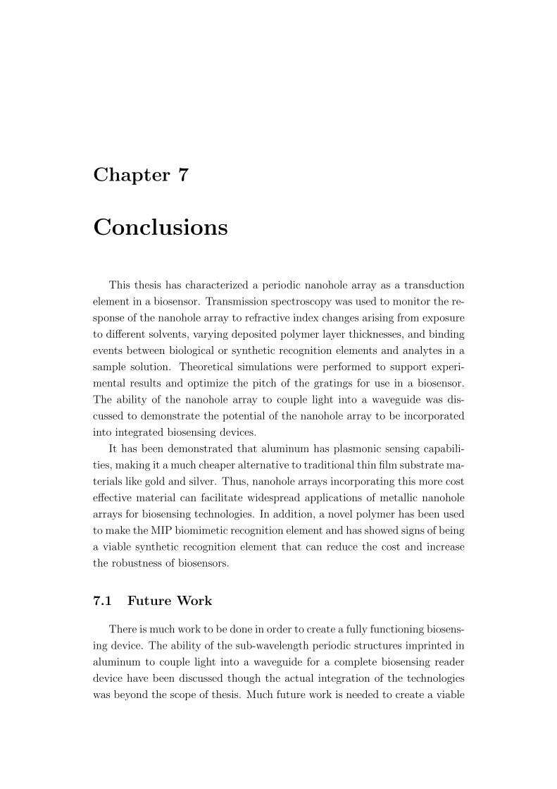
Chapter 7
Conclusions
This thesis has characterized a periodic nanohole array as a transduction
element in a biosensor. Transmission spectroscopy was used to monitor the re-
sponse of the nanohole array to refractive index changes arising from exposure
to different solvents, varying deposited polymer layer thicknesses, and binding
events between biological or synthetic recognition elements and analytes in a
sample solution. Theoretical simulations were performed to support experi-
mental results and optimize the pitch of the gratings for use in a biosensor.
The ability of the nanohole array to couple light into a waveguide was dis-
cussed to demonstrate the potential of the nanohole array to be incorporated
into integrated biosensing devices.
It has been demonstrated that aluminum has plasmonic sensing capabili-
ties, making it a much cheaper alternative to traditional thin film substrate ma-
terials like gold and silver. Thus, nanohole arrays incorporating this more cost
effective material can facilitate widespread applications of metallic nanohole
arrays for biosensing technologies. In addition, a novel polymer has been used
to make the MIP biomimetic recognition element and has showed signs of being
a viable synthetic recognition element that can reduce the cost and increase
the robustness of biosensors.
7.1 Future Work
There is much work to be done in order to create a fully functioning biosens-
ing device. The ability of the sub-wavelength periodic structures imprinted in
aluminum to couple light into a waveguide for a complete biosensing reader
device have been discussed though the actual integration of the technologies
was beyond the scope of thesis. Much future work is needed to create a viable
58 Chapter 7: Conclusions
label-free integrated optical waveguide bio(mimetic) sensor incorporating the
nanohole grating coupler and MIP as a recognition element. The novel MIP
polymer must be characterized and optimized for recognition of analyte, sta-
bility under a variety of environmental conditions, reusability, and interaction
with the nanohole refractive index grating sensor.
Further theoretical and experimental optimization of the nanohole arrays
must be performed to ensure maximum sensitivity and repeatability of results.
The effect of hole penetration into the aluminum substrate must be studied
to fully understand and optimize the imprinting process. Furthermore, the
optimal geometry of the holes should be studied to ensure maximum transmis-
sion and sensitivity . In order to successfully incorporate the nanohole array
and MIP technologies, the extent of polymer filling the holes must be deter-
mined to fully understand the effect of the polymer layer on the transmission
spectrum. Along the same lines, the extent of solvent filling the holes during
measurements should be studied.

Bibliography
[1] Ahmet A. Yanik, Min Huang, Osami Kamohara, Alp Artar, Thomas W.
Geisbert, John H. Connor, and Hatice Altug. An optofluidic nanoplas-
monic biosensor for direct detection of live viruses from biological media.
Nano Letters, 10(12):4962–4969, 2010.
[2] Matthew A. Cooper. Optical biosensors in drug discovery. Nature Reviews
Drug Discovery, 1:515–528, July 2002.
[3] G.M. Hwang, Lin Pang, E.H. Mullen, and Y. Fainman. Plasmonic sens-
ing of biological analytes through nanoholes. Sensors Journal, IEEE,
8(12):2074 –2079, dec. 2008.
[4] Hyungsoon Im, Si Hoon Lee, Nathan J. Wittenberg, Timothy W. Johnson,
Nathan C. Lindquist, Prashant Nagpal, David J. Norris, and Sang-Hyun
Oh. Template-stripped smooth ag nanohole arrays with silica shells for
surface plasmon resonance biosensing. ACS Nano, 5(8):6244–6253, 2011.
[5] A.G. Brolo. Plasmonics for future biosensors. Nature Photonics,
6(11):709–713, 2012.
[6] Gabriela Cervantes Tellez, Aftab Ahmed, and Reuven Gordon. Optimiz-
ing the resolution of nanohole arrays in metal films for refractive-index
sensing. Applied Physics A: Materials Science Processing, pages 1–6.
10.1007/s00339-012-7405-5.
[7] J.M. McMahon, J. Henzie, T.W. Odom, G.C. Schatz, S.K. Gray, et al.
Tailoring the sensing capabilities of nanohole arrays in gold films with
rayleigh anomaly-surface plasmon polaritons. Opt. Express, 15(26):18,
2007.
[8] Antoine Lesuffleur, Hyungsoon Im, Nathan C. Lindquist, Kwan Seop Lim,
and Sang-Hyun Oh. Plasmonic nanohole arrays for real-time multiplex
biosensing. pages 703504–703504–10, 2008.
59

60 BIBLIOGRAPHY
[9] Karsten Haupt. Peer reviewed: Molecularly imprinted polymers: The
next generation. Analytical Chemistry, 75(17):376 A–383 A, 2003.
[10] M. Yan and O. Ramstrom. Molecularly imprinted materials: science and
technology. CRC, 2004.
[11] CA Barrios, C. Zhenhe, F. Navarro-Villoslada, D. Lopez-Romero, and
MC Moreno-Bondi. Molecularly imprinted polymer diffraction grating
as label-free optical bio (mimetic) sensor. Biosensors and Bioelectronics,
26(5):2801–2804, 2011.
[12] D.R. Shankaran, K.V. Gobi, and N. Miura. Recent advancements in sur-
face plasmon resonance immunosensors for detection of small molecules
of biomedical, food and environmental interest. Sensors and Actuators B:
Chemical, 121(1):158–177, 2007.
[13] Inc. R D Sytems. Technical information: Detection visualization of
antibody binding, 2012.
[14] V. Espina, E.C. Woodhouse, J. Wulfkuhle, H.D. Asmussen, E.F. Petri-
coin III, and L.A. Liotta. Protein microarray detection strategies: fo-
cus on direct detection technologies. Journal of immunological methods,
290(1-2):121–133, 2004.
[15] B.B. Haab. Methods and applications of antibody microarrays in cancer
research. Proteomics, 3(11):2116–2122, 2003.
[16] Y. Fuchiwaki and I. Kubo. Electrochemical sensor based on biomimetic
recognition utilizing molecularly imprinted polymer receptor. 2010.
[17] M. Pohanka and P. Skladal. Electrochemical biosensors–principles and
applications. J Appl Biomed, 6(2):57–64, 2008.
[18] R. Karlsson, P.S. Katsamba, H. Nordin, E. Pol, and D.G. Myszka. An-
alyzing a kinetic titration series using affinity biosensors. Analytical bio-
chemistry, 349(1):136–147, 2006.
[19] E. Hecht. Optics. Addison-Wesley, 4th edition, 1998.
[20] F.M. Grimaldi. Adnexis. Bernia, 1665.
[21] T.W. Ebbesen, H.J. Lezec, H.F. Ghaemi, T. Thio, and P.A. Wolff. Ex-
traordinary optical transmission through sub-wavelength hole arrays. let-
ters to Nature, 391:667–669, 1998. 10.1038/35570.

BIBLIOGRAPHY 61
[22] Myeong-Woo Kim, Teun-Teun Kim, Jae-Eun Kim, and Hae Yong Park.
Surface plasmon polariton resonance and transmission enhancement of
light through subwavelength slit arrays in metallic films. Opt. Express,
17(15):12315–12322, Jul 2009.
[23] E.G. Loewen and E. Popov. Diffraction gratings and applications (optical
engineering, 58). 1997.
[24] C.H. Wilcox. Theory of bloch waves. Journal d’analyse mathematique,
33(1):146–167, 1978.
[25] H. Gao, JM McMahon, MH Lee, J. Henzie, SK Gray, GC Schatz,
TW Odom, et al. Rayleigh anomaly-surface plasmon polariton reso-
nances in palladium and gold subwavelength hole arrays. Opt. Express,
17(4):2334–2340, 2009.
[26] K.S. SreeHarsha. Principles of Physical Vapor Deposition of Thin Films.
Elsevier, 2006.
[27] Ian M. White and Xudong Fan. On the performance quantification of
resonant refractive index sensors. Opt. Express, 16(2):1020–1028, Jan
2008.
[28] F. Romanato, KH Lee, G. Ruffato, and CC Wong. The role of polarization
on surface plasmon polariton excitation on metallic gratings in the conical
mounting. Applied Physics Letters, 96(11):111103–111103, 2010.
[29] R. Jelinek. Cellular and Biomolecular Recognition. Wiley, 2009.
[30] A.E.G. Cass, T. Cass, and F.S. Ligler. Immobilized Biomolecules in Anal-
ysis: A Practical Approach. The Practical Approach Series. Oxford Uni-
versity Press, 1998.
[31] S. Herranz, M.D. Marazuela, and M.C. Moreno-Bondi. Automated
portable array biosensor for multisample microcystin analysis in fresh-
water samples. Biosensors and Bioelectronics, 33(1):50 – 55, 2012.
[32] Samuel Guillon, Remi Lemaire, Ana Valvanuz Linares, Karsten Haupt,
and Cedric Ayela. Single step patterning of molecularly imprinted poly-
mers for large scale fabrication of microbiochips. Lab Chip, 9:2987–2991,
2009.
62 BIBLIOGRAPHY
[33] B. Sellergren. Molecularly Imprinted Polymers: Man-Made Mimics of
Antibodies and Their Application in Analytical Chemistry. Techniques and
Instrumentation in Analytical Chemistry, V. 23. Elsevier Science Limited,
2001.
[34] Inc Filmetrics. Operations manual for the filmetrics f20 thin-film analyzer.
Technical report, Filmetrics, Inc.
[35] W. Yu. Parallel Finite-Difference Time-Domain Method. Artech House
Electromagnetic Analysis Series. Artech House, 2006.
[36] K. Yee. Numerical solution of initial boundary value problems involving
maxwell’s equations in isotropic media. Antennas and Propagation, IEEE
Transactions on, 14(3):302–307, 1966.
[37] Inc. Lumerical. Fdtd solutions user guide, 2003.
[38] L. W. Bos and D. W. Lynch. Low-energy optical absorption peak in
aluminum and al-mg alloys. Phys. Rev. Lett., 25:156–158, Jul 1970.
[39] L. Martin-Moreno, FJ Garcia-Vidal, HJ Lezec, KM Pellerin, T. Thio,
JB Pendry, and TW Ebbesen. Theory of extraordinary optical trans-
mission through subwavelength hole arrays. Physical review letters,
86(6):1114–1117, 2001.
[40] K. J. Klein Koerkamp, S. Enoch, F. B. Segerink, N. F. van Hulst, and
L. Kuipers. Strong influence of hole shape on extraordinary transmis-
sion through periodic arrays of subwavelength holes. Phys. Rev. Lett.,
92:183901, May 2004.
[41] K. L. van der Molen, K. J. Klein Koerkamp, S. Enoch, F. B. Segerink,
N. F. van Hulst, and L. Kuipers. Role of shape and localized resonances
in extraordinary transmission through periodic arrays of subwavelength
holes: Experiment and theory. Phys. Rev. B, 72:045421, Jul 2005.
[42] Jir Homola. Present and future of surface plasmon resonance biosen-
sors. Analytical and Bioanalytical Chemistry, 377:528–539, 2003.
10.1007/s00216-003-2101-0.
[43] H. Mukundan, A.S. Anderson, W.K. Grace, K.M. Grace, N. Hartman, J.S.
Martinez, and B.I. Swanson. Waveguide-based biosensors for pathogen
detection. Sensors, 9(7):5783–5809, 2009.

BIBLIOGRAPHY 63
[44] J.N. Yih, Y.M. Chu, Y.C. Mao, W.H. Wang, F.C. Chien, C.Y. Lin, K.L.
Lee, P.K. Wei, and S.J. Chen. Optical waveguide biosensors constructed
with subwavelength gratings. Applied optics, 45(9):1938–1942, 2006.