nanomagnetism research: benefit from reduced...
TRANSCRIPT

Nanomagnetism Research: Benefit From Reduced Dimensionality and Interfaces
by
Jie Wu
A dissertation submitted in partial satisfaction of the
requirements for the degree of
Doctor of Philosophy
in
Physics
and the Designated Emphasis
in
Nanoscale Science and Technology
in the
Graduate Division
of the
University of California, Berkeley
Committee in charge:
Professor Zi Qiang Qiu, Chair
Professor Ramamoorthy Ramesh
Professor Oscar Dubon
Spring 2010
Nanomagnetism Research: Benefit From Reduced Dimensionality and Interfaces
Copyright 2010
by Jie Wu
1
Abstract
Nanomagnetism Research: Benefit From Reduced Dimensionality and Interfaces
by
Jie Wu
Doctor of Philosophy in Physics
and the Designated Emphasis in Nanoscale Science and Technology
University of California, Berkeley
Professor Zi Qiang Qiu, Chair
Along the effort of integrating the spin degree of freedom in electronic devices, magnetic structures at the nanometer scale are intensely studied because of their importance in both fundamental research and technological applications. In this dissertation, I present my Ph.D research on several subjects to reflect the broad topics of nanomagnetism research. Single-crystalline, magnetic, ultrathin films are synthesized by Molecular Beam Epitaxy (MBE) and measured by state-of-art techniques such as Magneto-Optic Kerr Effect (MOKE), Photoemission Electron Microscopy (PEEM), X-ray Circular and Linear Dichriosm (XMCD and XMLD) Spectroscopy. First, I will present my work on the quantum well state in metallic thin films. Second, I will present my study on the magnetic long range order in two-dimensional magnetic systems, particularly on the observation of stripe and bubble magnetic phases and the universal laws governing the stripe-to-bubble phase transition. Third, I will present my result on a new type of magnetic anisotropy resulting from the spin frustration at ferromagnetic/antiferromagnetic interfaces. Fourth, I will present our studies on the mechanism of the abnormal interlayer coupling in ferromagnet/antiferomagnet/ferromagnet sandwiches structure. Fifth, I will show a new method to control the oxidation process to realize the control of exchange bias. Sixth, I will revisit the topic of exchange bias and show that the exchange bias actually takes place even before the antiferromagentic spins are frozen. In the last chapter, I will summarize my research and discuss the future of this exciting field.

i
Table of Contents Chapter 1 Introduction
1.1 Magnetic Storage Industry 1.2 Nanomagnetism and Spintronics
Chapter 2 Experimental Techniques
2.1 Molecular Beam Epitaxy 2.1.1 Basic concept 2.1.2 Ultrahigh Vacuum (UHV) system 2.1.3 Substrate Preparation 2.1.4 Sample growth
2.2 Sample Quality Characterization 2.2.1 Auger Electron Spectroscopy (AES) 2.2.2 Low Energy Electron Diffraction (LEED) 2.2.3 Reflection High Energy Electron Diffraction (RHEED) 2.2.4 Scanning Tunneling Microscopy (STM) 2.2.5 Atomic Force Microscopy (AFM)
2.3 Nano-fabrication Tools 2.3.1 Focused Ion Beam (FIB) 2.3.2 Lithography
2.4 Angle Resolved Photoemission Spectroscopy (ARPES) 2.5 Surface Magneto-Optic Kerr Effect (SMOKE) 2.6 Photoemission Electron Microscopy (PEEM) 2.7 Spin-Polarized Low Energy Electron Microscopy (SPLEEM)
Chapter 3 Retrieving the energy band of Cu thin films using quantum well states 3.1 Introduction 3.2 Experiment 3.3 Results and Discussion 3.4 Summary Chapter 4 Stripe-to-bubble transition of magnetic domains at the spin reorientation of (Fe/Ni)/Cu/Ni/Cu(001) 4.1 Introduction 4.2 Experiment 4.3 Results and Discussion 4.4 Summary Chapter 5 Magnetic frustration induced Ni spin switching in FeMn/Ni/Cu(001) 5.1 Introduction 5.2 Experiment 5.3 Results and Discussion 5.4 Summary

ii
Chapter 6 Element-specific study of the anomalous magnetic interlayer coupling across NiO spacer layer in Co/NiO/Fe/Ag(001) using XMCD and XMLD
6.1 Introduction 6.2 Experiment 6.3 Results and Discussion 6.4 Summary Chapter 7 Tailoring exchange bias by oxidizing Co film across a Cu wedge in
Cu(wedge)/CoO/Co/Cu(001) 7.1 Introduction 7.2 Experiment 7.3 Results and Discussion 7.4 Summary Chapter 8 A direct measurement of rotatable and frozen CoO spins in exchange bias system of
CoO/Fe/Ag(001) 8.1 Introduction 8.2 Experiment 8.3 Results and Discussion 8.4 Summary Chapter 9 Summary and Outlook

1
Chapter 1 Introduction The research on magnetic thin films and nanostructures has experienced fascinating progress in the last few decades and continues as an exciting research field. The driving force of this discipline is the ever-lasting demand of creative new technologies from the magnetic storage industry. As one of the biggest industry in the world, the magnetic storage industries plays an essential role in a modern society with wide impact on shaping the future of human beings. In this chapter, I will review the rapid development of the magnetic storage industry, highlight the newly adopted technologies and emphasize their contribution to the revolution of the industry. The history of this industry clearly demonstrates the close relation between the commercial products in the market and the fundamental research in the labs. It further reveals that the future of the magnetic storage industry should be based on today’s research on nanomagnetism and spintronics. 1.1 Magnetic Storage Industry
The hard disk drive (HDD) is a non-volatile storage device which stores digitally encoded data on rapidly rotating platters with magnetic surfaces. It provides efficient and reliable access to large volumes of data and is the main storage media used in desktop computers and laptops. In the 21st century, HDD usage expanded into consumer applications such as camcorders, cell phones (e.g. the Nokia N91), digital audio players, digital video players (e.g. the iPod Classic), digital video recorders, personal digital assistants, video game consoles, etc.[1]
Compared with its competitors, like flash memory and RAMs, HDD has its unique advantages. First, HDD is a non-violate storage method. No electrical power is needed to maintain the stored data. This feature makes HDD favorable for long term data storage.
Figure 1.1: HDD Roadmap.[2]

2
Second, the capacity and areal density of HDDs are large (as shown in Figure 1.1). As of April 2009, the highest capacity HDD was 2 TB. A typical "desktop HDD" might store between 120 GB and 2 TB although rarely above 500 GB of data rotate at 5,400 to 10,000 rpm and has a media transfer rate of 1 Gbit/s or higher. The areal density of disk storage devices has increased dramatically since IBM introduced the RAMAC, the first hard disk, in 1956. RAMAC had an areal density of 2,000 bit/in². Commercial hard drives in 2005 typically offered densities between 100 and 150 Gbit/in², an increase of about 75 million times over the RAMAC. In 2005 Toshiba introduced a new hard drive using perpendicular recording, which features a density of 179 Gbit/in². Toshiba's experimental systems have demonstrated 277 Gbit/in², and more recently Seagate Technology has demonstrated a drive with a 421 Gbit/in² density. It is expected that perpendicular recording technology can scale to about 1 Tbit/in² at its maximum.
Figure 1.2: Prices of HDD, DRAM, and Flash.[2]
Third, the HDD is economic in terms of cost per bit (as shown in Figure 1.2). The fact that the overall price has remained fairly steady has led to the common measure of the price/performance ratio in terms of cost per bit. IBM's RAMAC from 1956 supplied 5 MB for $50,000, or $10,000 per megabyte. In 1989 a typical 40 MB hard drive from Western Digital retailed for $1199.00, or $36/MB. Drives broke the $1/MB in 1994 and in early 2000 were about 2¢/MB. By 2004 the 250 GB Western Digital Caviar SE listed for $249.99, approaching $1/GB, an improvement of 36 thousand times since 1989 and 10 million times since the RAMAC. This is all without adjusting for inflation, which adds another factor of about seven times since 1956. It is also clear from Figure 1.2 that the cost per bit of HDDs is always at least one order of magnitude lower than that of DRAM and flash, making HDDs widely accepted for many usages.
Based on the above three reasons, HDDs cannot be replaced by any existing data storage method and will expand into more consumer applications. Market of HDD[3]
The HDD has a big market and makes very attracting profit. As an example, the HDD industry shipped 138 million drives in the third quarter of 2007, up 19.6 percent from 115

3
million drives in the second quarter. Combined third-quarter revenue for all HDD suppliers was $8.8 billion, up 22.2 percent from the second quarter. Leading HDD maker Seagate Technology LLC in the third quarter reported a gross margin of 24.6 percent - up 300 basis points from 21.6 percent in the second quarter. The second-ranked HDD supplier Western Digital Corp. (WDC) reported a gross margin of 18.4 percent - up 340 basis points from 15.0 percent in the second quarter. The number-three HDD maker Hitachi GST narrowed its losses to $58 million, down from -$174 million in the second quarter, and projected an optimistic fourth quarter with a profit estimate of more than $9 million.
The worldwide HDD industry experiences sustained unit and revenue growth through 2009, with particularly strong expansion of the consumer electronics (CE) and external drive/home storage segments. Given the projected 14-percent annual growth rate in the disk storage market from 1997 to 2001, one additional percentage point in market share could have a billion-dollar impact. Moreover, a substantial improvement could enable entirely new computing applications, with spillovers across the computer industry and every industry that uses magnetic recording to store data. Driving force of HDD industry
The Moore’s law has held for hard disk storage cost per unit of information. The rate of progression in disk storage over the past decades has actually sped up more than once, corresponding to the utilization of error correcting codes, the magnetoresistive effect and the giant magnetoresistive effect. The current rate of increase in hard drive capacity is roughly similar to the rate of increase in transistor count. Recent trends show that this rate has been maintained into 2009.
Figure 1.3: The Moore’s law for HDD areal density.[2]
Hitachi HDD's areal density is shown in Figure 1.3 to demonstrate the exponential increase in areal density of HDDs and the driving technologies. Areal density has increased by a

4
factor of 35 million since the first disk drive, RAMAC, was introduced in 1957. Since 1991, the rate of increase has accelerated to 60% per year, and since 1997 this rate has further accelerated to an incredible 100% per year. This acceleration is the result of the introduction of MR read heads in 1991, GMR read heads in 1997 and AFC media in 2001, all of which were first introduced by Hitachi GST. It is of interest to consider future areal density growth and the technology requirements to maintain this growth. Generally, the industry expects areal density to continue to increase to 100 Gbits/in2 and beyond but at a somewhat lower growth rate.
From above observation, we can easily realize it is the new adopted technologies that support the rapid development in the aeal density. In short, new progresses in record media, read head and fabrication methods dominate the HDD industry. As a good example, the adoption of GRM heads by the industry is shown in Figrue 1.4.
Figure 1.4: Industry adoption of GMR heads by quarter.[3]
Earlier than the second quarter of 1998, no GMR heads were produced in a commercial product. As a contrast, by the first quarter of 2000, GMR heads took all the market shares. This dramatic change took place in a span of less than two years. It is a great example that illuminates the intense competition in the HDD industry and the extreme importance of developing and adopting new technologies. Therefore, it is safe to say that the investments on possible future technique are the key for all the companies to survive and grow in HDD industry.
1.2 Nanamagnetism and spintronics
When the size of magnetic structures shrinks down to the nanometer scale, its magnetism changes drastically. The lower dimensionality and the interface plays an essential role, giving rise to numerous new phenomena that appear only at this length scale but don’t occur in bulk materials, such as spin reorientation transition (SRT) and magnetic vortex. Intense research has been devoted to the study of nanomagnetism but the complexity of magnetic systems still demands more effort. The fundamental reason is as following: electrons have both “charge” and “spin”. From a theoretical point of view, the charge corresponds to a scalar, and the transportation of charge is protected by the conservation of charge; meanwhile the spin corresponds to a vector, and it is a indeed one kind of angular momentum which means it could be transferred into other kinds of angular momentum. Therefore spin itself is not conserved

5
under most of circumstances. By manipulating the charge, people have achieved many wonders including all the electronic devices today. By manipulate the spin, our capability can be further extended because a vector can contain much more information than a scalar. This is the original thought of the so called spintronics. Spintronics is an area that is changing fast and has many possible directions to develop. Here I only give one example of the new interesting discoveries in this field. Spin Hall Effect (SHE)
In analogy to the conventional Hall effect, the spin Hall effect has been proposed to occur in paramagnetic systems as a result of spin-orbit interaction, and refers to the generation of a pure spin current transverse to an applied electric field even in the absence of applied magnetic fields. Hence there will be spin accumulation at the edges of the sample: there will be an excess of spin up electrons on one side and an excess of spin down electrons on the other side (Figure 1.5).
Figure 1.5: In the Hall effect the Fermi levels for up and down electrons are the same, and the difference in the Fermi levels at both edges of the sample is the Hall voltage VH. In the spin Hall effect the difference in the Fermi levels for each spin at both edges of the sample is VSH, but it is of opposite sign for spin up and down electrons.[4]
Until today, many experiments showed the evidence of the presence of SHE. Here I just mention the first one of them very briefly.[5]
Figure 1.6: (Left) Schematic of the unstrained GaAs sample and the experimental geometry. (Right) Two-dimensional images of spin density ns and reflectivity R, respectively, for the unstrained GaAs sample measured at T 0~30 K and E=10 mV um–1.[5]

6
N type GaAs was grown on (001) semi-insulating GaAs substrate by molecular beam epitaxy. Standard photolithography and wet etching are used to define a semiconductor channel (Fig 8.2 left). It’s clear that the spin density ns is nonzero only at two edges of the sample and even changes the sign under the Kerr microscopic (Fig 8.2 right). Further results show that by reversing the direction of electrical field, spin up and spin down accumulation exchange their position.
In spite of the solid experimental proof, the origin of SHE has been under controversy for a long time till today. As far as I know, at least three main theories have been proposed to account for SHE but theorists can’t reach agreement even on very fundamental questions, like the intrinsic or extrinsic nature of SHE. Limited by the volume of this chapter, I’ll skip the discussion on the possible mechanism responsible for SHE.
From the above introduction, I have illustrated the close relation between the magnetic storage industry and the research on nanomagnetism and spintronics. In the following chapters, I will present our studies on a variety of perspectives of nanomagnetism.
7
Chapter 2 Experimental techniques
A successful experiment consists of sample synthesis, sample structure characterization, and measurements on magnetic properties.
The sample synthesis method for my work is mainly based on molecular beam epitaxy (MBE) technique. MBE is a very clean tool to synthesis thin films and multilayers with a good crystalline quality which are all single crystals within the scope of this thesis. The single crystal sample has big advantage compared to a polycrystalline sample. First, the magnetic anisotropy is related to the orientation of the lattice and thus can only be studied using single crystal film. Second, the X-ray linear dichrism (XMLD) effect is sensitive to the lattice orientation as well that it only manifest itself in a single crystal. Third, in general a single crystal film is flat at nanometer scale, reducing the effect of surface roughness and interfacial mixing. Therefore, a single crystal sample can provide a unique way to the solution of many puzzles in magnetism research.
The characterization of the sample structure is carried out by several tools compatible with ultrahigh vacuum system that is discussed in detail in the following paragraphs. The purpose is to confirm the single crystal nature of the samples, detect the alignment of the sample lattice, and further study the surface morphology.
The magnetic properties are measured with the state-of-art methods that can be found the third section of this chapter. It combines the tools for magnetic microscopy and magnetic spectroscopy. 2.1 Molecular beam epitaxy (MBE) General concept
MBE takes place in ultrahigh vacuum system (UHV). By evaporating materials slowly (usually in the order of 0.1 nm per minute), the deposited atoms are given enough time to relax to an equilibrium position on top of a given substrate and form a nice lattice of single crystal.
The structures formed by the deposited atoms are influenced by the choice of the substrate. The atoms on the surface of the substrate play a role as a template for the deposited atoms so the lattice of deposited atoms has the tendency to follow the lattice of the substrate. In this way a new structure of one material that doesn’t exist in a bulk, can be stabilized by a right choice of the substrate. For instance, the ground state of Fe in a bulk is body-centered cubic (bcc) structure. However, Fe grown on a Cu(001) substrate forms a face-centered cubic (fcc) structure under the growth temperature of 90 K. Thus the strong electronic interaction between interfacial Fe and Cu atoms changes the meatastable fcc phase to a ground phase.
Even the structure of deposited atoms is the same as its structure of a bulk, the film obtained by MBE is still different from a free-standing film. In other words, the influence of the substrate in most cases should be taken into account. The reason is that the lattice parameter of the deposited film is, in general, different from the lattice parameter of the substrate. The mismatch between two lattices usually introduces a tension in the epitaxy film that could affect the magnetism of the thin film. A good example is NiO. When NiO is grown on top of Ag(001) substrate, NiO spins are aligned in-plane; for NiO grown on top of MgO(001) substrate, NiO spins are aligned out-of-plane.
8
Ultrahigh Vacuum (UHV) system The ultra thin metallic film must be grown and kept at ultrahigh vacuum because the film
is composed of only several atomic layers and if it is exposed to air, the film will be easily contaminated or oxidized. If the pressure is 10-10torr, the time is order of an hour. Though some samples are exposed to air while being transported from the growth chamber to the experiment chamber, the ultrahigh vacuum is the most basic condition for ultra thin film experiment. When the sample has to be out in air, noble metals such as Ag, Au and Cu must be capped to prevent oxidization or contamination. At least several nanometers of capping layer is necessary for layer by layer grown ultra thin film.
To get ultrahigh chamber three states of pumping are required. First a mechanical pump is used to get pressure down to 10-3 torr range (mid vacuum). Second, a turbo pump backed by a mechanical pump can bring the pressure down to 10-7 torr range (high vacuum). The turbo pump rotates its blades as fast as tens of thousands rpm to pump the air out. Then finally, the ion pump is used to bring the pressure down to the ultrahigh vacuum level. The ion pump permanently traps the molecules chemically. First the atoms of the gas are ionized by electrons which are emitted from the cathode discharge and accelerated by electric and magnetic field. And the ionized gas atoms are accelerated by electric field and absorbed into the reactive metals like tantalum and titanium. Another type of pump, which is used temporarily but is effective in lowering the pressure quickly, is titanium sublimation pump or TSP. The titanium filament inside a vacuum chamber is heated up with large current (40-50A) for a couple of minutes. Then the titanium evaporates onto the inside wall of the chamber and the freshly exposed titanium surface traps the gas molecules by forming alloys with the ones that come in contact with.
There are many kinds of gauges to measure the pressure of vacuum chamber. Two kinds of gauges are most often used. One is the Pirani gauge (thermo gauge) which measures down to 10-3torr. Since the gauge only covers low vacuum range, it is often used to check the vacuum between a mechanical pump and a turbo pump. The Pirani gauge head is based around a heated wire placed in a vacuum system, the electrical resistance of the wire being proportional to its temperature. At atmospheric pressure, gas molecules collide with the wire and remove heat energy from it (effectively cooling the wire). As gas molecules are removed (i.e. the system is pumped down) there are less molecules and therefore less collisions. Fewer collisions mean that less heat is removed from the wire and so it heats up. As it heats up, its electrical resistance increases. A simple circuit utilizing the wire detects the change in resistance and once calibrated can directly correlate the relationship between pressure and resistance. In this way you can use a calibrated meter to indicate pressure.
The pressure of ultrahigh vacuum chamber can be measured by the ion gauge. The ion gauge consists of three distinct parts, the filament, the grid, and the collector. The filament is used for the production of electrons by thermo-ionic emission. The grid has positive voltage which pulls the electrons from the filament. Electrons circulate around the grid passing through the fine structure many times until eventually they collide with the grid. Gas molecules inside the grid may collide with circulating electrons. The collision can take an electron from the gas molecule and make it positively ionized. The collector inside the grid has negative voltage and attracts these positively charged ions. The number of ions collected by the collector is directly proportional to the number of molecules inside the vacuum system. By this method, measuring the collected ion current gives a direct reading of the pressure. Substrate preparation

9
Cu(001) single crystals are commercially available, but in many cases, more steps of polishing are required to use it as a substrate for ultrathin films. This is because the Cu is a soft metal, so the Cu surface can be easily scratched and contaminated after several uses. The first stage of polishing is the mechanical polishing. For the mechanical polishing, the substrate is mounted on an epoxy and ground into the desired shape with fine sandpaper. When necessary, a flat surface can be shaped into a stepped or curved surface during this process (The details of polishing a flat Cu substrate into a stepped or curved substrate will be introduced in Chapter 5). After mechanical polishing, the substrate goes through three stages of diamond paste polishing with increasingly finer grain size of 6 micron, 1 micron, and 0.25 micron. After the 0.25 micron mechanical polishing, the surface should have a mirror-like finish and the crystal is taken out of the epoxy by melting it in acetone. Though it has a mirror like surface, the surface may not be very clean and flat because small particles of Cu may fill the scratches or defects in the Cu substrate to make the surface look clean and flat. So electrochemical polishing is required to remove these small particles from the Cu substrate. In addition, the surface roughness can be further reduced by electrochemical polishing. The following method was used for the electrochemical polishing of Cu substrates. Before doing the electrochemical polishing, the substrate must be cleaned with water and acetone in an ultrasonic cleaner. (1) Mix 40 ml phosphoric acid (85%), 9 ml water, and 5 ml sulfuric acid (98%). First, add phosphoric acid to the water and then the sulfuric acid to the mixture. (2) Set the voltage of power supply to 1.8V and turn it off. Put a Cu cathode into solution and connect the anode to the cleaned and dried substrate and put it into the solution. (3) Turn on the power supply and apply 1.8V of constant voltage between the cathode and the crystal. Make sure to apply positive to the crystal and ground to the solution. (4) As soon as the voltage is applied, bubbles should form around the crystal and the cathode. After ~20 seconds when the current drops and stabilizes, take the crystal out of the solution and immediately rinse with distilled water followed by ultrasound. Then, rinse and ultrasound with acetone.
After the electrochemical polishing the Cu substrate should look clean with very few defects. Sometimes after this process the surface may have cloudy patterns. When observed under an optical microscope the cloudy patterns are found to be many small defects on the substrate due to rough mechanical polishing. In this case, the mechanical polishing and electrochemical polishing should be repeated to obtain a flat and clean Cu substrate. Repeating only the electrochemical polishing does not totally remove the cloudy patterns.
The Cu(001) substrate was then introduced into an ultrahigh vacuum (UHV) chamber with a base pressure in the low 10-10 torr range. Ultrathin metallic films must be deposited and kept in UHV because the film is composed of only several atomic layers, which can be easily contaminated or oxidized when exposed to air. Before the sample growth, the Cu substrate goes through the final stage of cleaning inside the UHV chamber. First, the substrate is sputtered by Ar+ ions with high kinetic energy (1~5keV). The bombarded Ar+ ions remove the contaminant rich top layers. Ar is chosen for sputtering because it is a noble gas, which does not interact chemically with other material. This chemical inertness ensures that the Ar+ ions themselves do

10
not become a contaminant either by staying on the surface of the substrate during sputtering or by being absorbed on the inside surface of the UHV chamber. For the same reason, the Ar gas cannot be effectively removed by the ion pump. Ar is only held at the cathode of the ion pump by a weak force, preventing the surface refreshing process of ion pump. So, the ion pump must be deactivated during the sputtering process. Closing the valve to the ion pump or turning the ion pump off is necessary.
Although, the sputtering process removes the contaminated top layers of the substrate, it also makes the surface rough. In order to smooth the surface after sputtering, the substrate is annealed to ~600ºC and cooled down slowly. During the annealing process, the constituent atoms have high mobility so that mechanical stress can be relieved and defects removed. The slow cooling gives the atoms enough time to settle in a position where they have the lowest energy and arrange themselves into the crystal structure. Several cycles of sputtering and annealing are necessary before one can obtain a clean and well-ordered surface. Sample growth
The epitaxial (layer by layer) growth of thin films was achieved by molecular beam epitaxy (MBE) in a UHV chamber. The adsorbed atom from the MBE evaporator will not always grow epitaxially on top of the substrate. In fact growing a single crystalline film on top of a preexisting crystal is not so straightforward. To achieve epitaxial growth, the substrate-adatom adhesion energy needs to be quite large (~ -1 to -10 eV / atom). If the surface adhesion energy is not so strong, the film will most likely grow three dimensionally in clusters to reduce the surface contact area with the substrate. If the substrate-adatom adhesion energy is strong, i.e. comparable to the adatom-adatom adhesion energy, and other conditions such as similar lattice symmetry and low lattice mismatch are satisfied, then there will be epitaxial growth.
There are two types of MBE evaporators that were used for this dissertation: thermal evaporators and e-beam evaporators. The thermal evaporators consist of an aluminum oxide crucible held inside a coil of tungsten wire. The tungsten wire is heated by flowing electrical currents around 10~20A. To reduce the degassing, the crucibles are enclosed by a tantalum shell to reflect radiation inward. In an e-beam evaporator, the thermally emitted electrons from a thoriated tungsten filament are accelerated toward the material by applying high voltage between the filament and the material. The kinetic energy of electrons is transferred into thermal energy to evaporate the material. For both types of evaporators, the whole evaporator is surrounded by a water cooling jacket to reduce the degassing. The evaporators must be fully degassed before the growth of the sample.
The deposition rate is monitored by a quartz crystal oscillator. The quartz oscillator measures the surface phonon frequency, which decreases with the deposition of materials on the quartz due to the change of mass. Typical deposition rates for ultrathin films are 0-3 Å/min. After applying current to the evaporator, the deposition rate needs to be stabilized before the growth of the sample. The growth time is calculated by dividing the desired thickness of the sample by the growth rate. During the deposition, the growth rate can be more accurately determined by using reflection high energy electron diffraction (RHEED). In addition, RHEED patterns are used to verify layer by layer growth. The RHEED intensity shows oscillations since ad-atoms on the flat surface have partial destructive interference. Then each oscillation corresponds to the completion of a full atomic layer.
A distinguishing feature of our research is the use of wedge shaped samples for a systematic thickness dependent study. This is useful since many physical parameters such as

11
Curie temperature, magnetic anisotropy, crystal structure, and interlayer coupling are functions of the thickness of the magnetic films. Wedges were created by moving the substrate behind a knife edge shutter during deposition. Since the slope of the wedge is ~ML/mm, locally the film is flat even for wedge samples. Therefore a wedge sample gives an infinite set of uniform films. It also guarantees the growth condition and substrate quality are the same for the regions of the wedge sample with different thickness, which is not true if separate samples are made for each film thickness. In addition, double wedges allow two film thicknesses to be varied independently by growing the two wedges along orthogonal directions. 2.1 Sample Quality Characterization
The characterization of the substrate and the sample includes both the chemical characterization and the structure characterization. The purpose of the chemical characterization is to identify the chemical elements on the surface that is carried out by the Auger Electron Spectroscopy (AES). The structure characterization is to identify the surface structures, including the crystalline structure and the surface orientation that is realized by the Low Energy Electron Diffraction (LEED), Reflection High Energy Electron Diffraction (RHEED) and Scanning Tunneling Microscopy (STM). Limited by the volume of this thesis, I will only briefly mention the principles of the above techniques. More thorough discussions on these techniques could be found in popular textbooks. Auger Electron Spectroscopy (AES)
The Auger electron spectroscopy technique for chemical analysis of surfaces is based on the Auger radiation process. The principle of AES is shown in the diagram.
Figure 2.1: (from internet) the diagram of Auger process.
When a core level of a surface atom is ionized by an impinging electron beam, the atom may decay to a lower energy state through an electronic rearrangement which leaves the atom in a doubly ionized state. The energy difference between these two states is given to the ejected Auger electron which will have a kinetic energy characteristic of the parent atom. When the Auger transitions occur within a few angstroms of the surface, the Auger electrons may be ejected from the surface without loss of energy and give rise to peaks in the secondary electron energy distribution function. The energy and shape of these Auger features can be used to unambiguously identify the composition of the solid surface.
Because the Auger peaks are superimposed on a rather large continuous background, they are more easily detected by differentiating the energy distribution function N(E). Thus the conventional Auger spectrum is the function dN(E)/dE. The peak-to-peak magnitude of an Auger

12
peak in a differentiated spectrum generally is directly related to the surface concentration of the element which produces the Auger electrons.
Here I give an example of Auger spectrum from my experiment.
Figure 2.2: The Auger spectrums obtained on a Cu(wedge)/Co/Cu(001) sample as a function of Cu thickness after exposed to oxygen.
The peaks in spectrums at different energies correspond to the signal from different chemical elements. For instance, around 500 eV corresponds to O, 650-800 eV corresponds to Co and 800-950 eV corresponds to Cu. One element could have several discrete peaks. The peak height measures the amount of the element on the surface. In the above figure, it can be concluded that Cu peaks increases while Co peaks and O peaks decreases as Cu layer gets thicker. This reflects the change of chemical compounds at the surface. Low Energy Electron Diffraction (LEED)
Low-energy electron diffraction (LEED) is a technique for the determination of the surface structure of crystalline materials by bombardment with a collimated beam of low energy electrons (20-200eV) and observation of diffracted electrons as spots on a fluorescent screen. Generally, the structural information given by a LEED pattern results from the position and the intensity of the diffraction spots as well as from the spot profiles. In particular, the surface unit cell of the reciprocal lattice and the corresponding real space unit cell follow from the positions of the LEED spots. From the spot profiles the quality and degree of long range order at the surface can be deduced. Surface sensitivity of LEED is determined by the scattering cross section of electron. Since LEED uses elastically diffracted electrons, both its incoming and outgoing electrons have a large back scattering cross section, thereby contributing to the surface sensitivity.
Here gives an example of LEED patterns obtained in my experiment.

13
Figure 2.3: The LEED patterns before and after oxygen exposure as a function of Cu thickness.
The LEED patterns show a change before and after oxidation. It indicates the crystalline structure of the bilayer has been changed by the oxidation process. For both LEED patterns taken after oxidation, the LEED patterns show a difference. The left LEED pattern after oxidation mainly follows the LEED patterns taken before oxidation, confirming a similar surface structure. Meanwhile, the right LEED patterns after oxidation is different from the one taken before oxidation, indicating a reconstruction of surface structure. Reflection High Energy Electron Diffraction (RHEED)
Another tool that can be used to characterize the surface is RHEED (reflection high energy electron diffraction). RHEED uses high-energy electrons (~10keV) reflected off the sample surface at a grazing angle (a few degrees). Basic principle of RHEED is same as LEED. Reflected image forms a series of lines since many diffraction spots lie on a line due to the shorter de Broglie wavelength of the electrons. The width of the lines shows the diffraction from different lateral crystal lines along the electron beam direction. For Cu(100), the lines are most clear and the width between the lines are short when the electron beam comes to the [110] direction. A flat surface gives uniform and bright lines but a rough surface does not. RHEED can be measured during sample growth since the electron comes from a grazing angle and material sources are not blocked by RHEED instruments. Since ad-atoms on the flat surface will give partial destructive constructions on the RHEED lines, the intensity of reflected electron oscillates with a monolayer period. Thus, RHEED can be used to monitor the thickness of a sample and to check the growth properties. The surface sensitivity of RHEED comes from the glancing angle at which the electrons are reflected because at glancing angle, the momentum of the electron along the direction normal to the sample surface is small, though the energy of electron is high. Though the energy of electrons is high, it is still safe to use RHEED during the growth of a sample, because it does not change the properties of the substrate or the sample due to its small mass. Scanning Tunneling Microscopy (STM)
In Scanning Tunneling Microscopy (STM) an electrically biased tip is scanned across a surface at a very close distance (about an atomic diameter). The current flow between the tip and the sample (due to the tunneling effect) strongly depends on the tip-surface gap and can be measured with great accuracy. The changing current signal can in turn be used to generate a surface topography map. In contrast to Atomic Force Microscopy (AFM) this method only works with conducting samples, e.g. metals, graphite, semiconductors.

14
Figure 2.4: (from internet) A diagram of STM setup.
The facility I use is the Omicron VT STM combined with VT Beam Deflection AFM. The temperature of the sample mounted on STM can be tuned from 25 K to 1500 K. However, the temperature of the tip is always kept at room temperature. Thus our STM is more suitable for the study of the surface morphology rather than the spectroscopy study (dI/dV).
Figure 2.5: STM image of Si(111) surface.
Here is an example of STM image on the famous (7*7) surface reconstruction of Si(111) surface taken in my lab. Atomic Force Microscopy (AFM)
In Atomic Force Microscopy (AFM) a tip is scanned across a surface at close distance tracing the surface contour. Inter-atomic, frictional, magnetic and electrostatic forces attract or repel the tip, which is mounted to a flexible cantilever. The resulting deflection of the cantilever can in turn be sued to produce an image of the surface, e.g. by generating lines of equal force. Commercially available are cantilever tips made from silicon nitride and silicon single crystals with various spring constants, resonance frequencies and coatings.

15
AFM can work in two modes. In AFM contact mode, the cantilever touches the surface during scanning the feedback signal is derived from the normal force, i.e. the force component perpendicular to the surface. In AFM noncontact mode, the feedback signal is derived from the force induced shift in resonance frequency of the vibrating AFM cantilever.
Here shows an example of AFM image obtained in non-contact mode.
Figure 2.6: The AFM image of the scratched structure of CoO/Fe/Ag(001) sample.
The AFM image shows the morphology of this post-fabrication CoO/Fe/Ag(001) sample. It clear shows that the center disk of CoO/Fe bilayer is preserved after the fabrication; meanwhile a ring shape materials is completely removed. The line profile further measures the depth of the milling process. 2.3 Nano-fabrication tools
By MBE, we are able to obtain atomic-flat thin films with sub-nanometer accuracy in controlling the film thickness. To form a three-dimensional nanostructure, some special techniques are employed to generate in-plane patterns. So far, all the techniques fall into two categories: self-assembly and nano-fabrication.
The self-assembly starts with a flat substrate and by choosing the growth condition, the atoms deposited onto the substrate have the preference to form clusters with certain shapes. The advantage of self-assembly is that it is a very clean technique because the deposition of atoms usually happens under high vacuum. Another advantage is that self-assembly is capable of making atom clusters with a small number of atoms. The disadvantage is that self-assembly is system-dependent and only a limited number of epitaxy systems can achieve it.
The nano-fabrication process, including focused ion beam (FIB), photolithography, e-beam lithography and other techniques, is a very useful tool in nanoscience and still under fast development. It is capable of making all possible desired patterns on almost all kinds of materials. However, the biggest withdraw of nanofabrication is the damage during the fabrication process could modify the properties under study. In this thesis, I focus on two major nanofabrication

16
techniques: FIB and photolithography, and shows an example of the damage on the magnetism due to FIB. Focused Ion Beam (FIB)
The principle of FIB is scratched in the following diagram.
Figure 2.7: (from wiki) A diagram of the mechanism of FIB.
An ion beam (usually Ga+ ion) is focused and scanned on top of the sample. Since ion has a comparable mass with the targeted atoms so it can transfer a big enough momentum to the targeted atoms, breaking the lattice and forcing targeted atoms to leave the sample surface. By scanning the focused ion beam, the machine writes a pattern with atom vacancy. The whole procedure is similar to a sputtering process. The only difference is that FIB is doing sputtering locally.
Figure 2.8: (from wiki) A schematic drawing of FIB components.

17
The above shows a schematic drawing of a FIB gun. Most FIB instruments using Liquid-metal ion sources (LMIS), especially gallium ion sources. Ion sources based on elemental gold and iridium are also available. In a Gallium LMIS, gallium metal is placed in contact with a tungsten needle and heated. Gallium wets the tungsten, and a huge electric field (greater than 108 volts per centimeter) causes ionization and field emission of the gallium atoms. Source ions are then accelerated to an energy of 5-50 keV (kiloelectronvolts), and focused onto the sample by electrostatic lenses. LMIs produce high current density ion beams with very small energy spread. A modern FIB can deliver tens of nanoampers of current to a sample, or can image the sample with a spot size on the order of a few nanometers.
The machine I use is FEI Strata 235 Dual Beam FIB located at the National Center for Electron Microscopy (NCEM) of Lawrence Berkeley National Laboratory (LBNL). The Dual Beam system contains both a focused Ga+ ion beam and a field emission scanning electron column. The ion column can be used for selective removal of material by ion beam milling. In addition, the ion beam can be used for ion-enhanced imaging of fine texture analysis in crystalline materials. The high resolution field emission electron beam can be used for chemical analysis through either electron dispersive spectroscopy or z-contrast imaging using a scanning transmission electron microscope (STEM) detector.
Figure 2.9: An example of the patterns fabricated by FIB.
The above figure is taken during one of my experiments. The figure shows three Secondary Electron Microscopy (SEM) images on three patterns ion milled for increasing time. It’s clear that ion milling removed more and more materials as time accumulates. The
18
remarkable fact is that the boundary of the pattern is kept very sharp all the time and no visible damage is observed for the center disk. Lithography
Lithography is a standard top-down fabrication method. It has different names depending on the source of the light. In this thesis, my experiment mainly uses optical lithography and e-beam lithography. Here I only discuss optical lithography since the principles of those two are very similar to each other.
The optical lithography uses light to transfer a geometric pattern from a photo mask to a
light-sensitive chemical photo resist on the substrate. The basic procedure includes the following: 1. Deposition of the photoresist.
Photoresist is deposited on the surface of the sample by so called “spin coating” to produce a uniform thick layer. The spin coating typically runs at 1200 to 4800 rpm for 30 to 60 seconds, and produces a layer between 0.5 and 2.5 micrometres thick. The spin coating process results in a uniform thin layer, usually with uniformity of within 5 to 10 nanometres. During the coating, my metallic substrate is heated to around 90oC to make a tighter bonding with the photoresist.
2. Exposure to light. The photoresist-coated sample is exposed to the light passing through a mask. The mask used is commercially made and has a 4:1 ratio to the desired patterns.
3. Developing of the patterns The sample is dipped into a photoresist developer to remove the photoresist on the regions that has been exposed to the light.
4. Ecthing Ion milling is conducted to imprint the patterns of the photoresist onto the sample. The reason that I choose ion milling rather than a chemical wet etching is chemical wet etching produces uncontrollable damage to the magnetism of my sample as confirmed by later PEEM measurement.
5. Photoresist removal The removal of the photoresist requires a liquid "resist stripper", which chemically alters the resist so that it no longer adheres to the substrate.
2.3 Angle Resolved Photoemission Spectroscopy (ARPES) ARPES is a direct experimental technique to observe the distribution of the electrons
(more precisely, the density of single particle electronic excitations) in the reciprocal space of solids. ARPES is one of the most direct methods of studying the electronic structure of the surface of solids.

19
Figure 2.10: A diagram of photoemission process.
A three steps model is generally accepted to interpret the photoemission process. Within this approach, the photoemission process is subdivided into three independent and sequential steps:
(i) Optical excitation of the electron in the bulk. (ii) Travel of the excited electron to the surface. (iii) Escape of the photoelectron into vacuum. The total photoelectron intensity is given by the product of three independent terms: the
total probability for the optical transition, the scattering probability for the traveling electrons, and the transmission probability through the surface potential barrier. Step (i) contains all the information about the intrinsic electronic structure of the material. Step (ii) can be described in terms of an effective mean free path, proportional to the probability that the excited electron will reach the surface without scattering. Step (iii) is described by a transmission probability through the surface, which depends on the energy of the excited electron as well as the material work function.
Figure 2.11: A schematic drawing of ARPES facility.

20
The above figure shows the basic setup of ARPES measurement. A photon beam with tunable energy hit the sample surface and knocks off some electrons out in a so called photoemission process. By making a full analysis of the outcoming electrons and applying the momentum and energy conservation laws, the band structure of the materials under study can be mapped out.
A good reference of this technique can be found at Reviews Of Modern Physics Volume: 75 Issue: 2 Pages: 473-541. 2.4 Surface Magneto-Optic Kerr Effect (SMOKE)
SMOKE or MOKE is a very convenient and sensitive tool to study the magnetism of a surface. It utilized the laser to detect the rotation in the light polarization before and after being reflected by the sample surface.
The microscopic origin of the magneto-optical Kerr effect is the spin-orbit interaction. The coupling between the aligned spins and the electron generates different energy levels for different orbital states which interact with the polarization of light differently. In this picture, electrons that are orbiting in clockwise and counterclockwise directions make different response to the light. Thus, the optical response, such as the speed and the absorption coefficient of light in the media, is different for left circular and right circular polarized light. When the linearly polarized light, which is a superposition of the left and right circularly polarized light, is reflected from the magnetic surface, the difference in the phase shifts of the left and right circularly polarized components result in the rotation of the linearly polarized light. This effect gives the Kerr rotation. Similarly, the difference in the absorption coefficient of the left and right circular polarized components gives the Kerr ellipticity.
Figure 2.12: Experimental setup of SMOKE.
The above scratches the experimental setup of SMOKE. A linearly polarized light (1mW He-Ne laser with wavelength of 632.8nm) was intensity stabilized and focused onto the sample
sample
quarter wave plate
analyzer (polarizer)
UHV window UHV window
lens
photodetector
lens
polarizer
He-Ne laser
longitudinal
polar H

21
(beam size~0.2mm). Then the reflected light goes through a quarter-wave plate, second polarizer(analyzer), focusing lens, and a photodetector.
The first step of the experiment is to minimize the reflected beam by adjusting both the analyzer and the quarter wave plate. In this “extinction” configuration, the polarization axis of the first polarizer (e.g. s-polarization) is perpendicular to the second polarizer (e.g. p-polarization).
At the extinction condition, the Kerr signal can be measured, but this measurement geometry has disadvantages. The intensity of the reflected light is proportional to the square of
the magnetization (22
~~ QEI ) because the minimum of the intensity means the first
derivative of the intensity is zero. This disadvantage can be circumvented by rotating the analyzer a small angle δ away from extinction. Then, the intensity measured by the
photodetector becomes linearly dependent on the magnetization
)("2)( 00
MIIMII .
Here I0 is the average background signal as 22
0 pEI , )(" M is the Kerr ellipticity and M is
the longitudinal or polar component of the magnetization. Thus the, longitudinal (polar) magnetic hysteresis loops can be obtained by sweeping a longitudinal (polar) magnetic field while measuring the intensity I(M) with the photodetector. Since the hystresis loop sweeps from the negative saturation to positive saturation, the overall change in the intensity over a hystresis
loop is
)("4~
)()(
0
..
0
M
I
MIMI
I
I satsat
. Note that the choice of δ is not unique and
depends on several factors. δ must be larger than )(' M and )(" M for linearity (and
therefore less noise), but larger δ reduces the change in the light intensity due to the Kerr signal. Thus, these two effects need to be balanced, and experimentally the optimal value of δ is about 1~2°. 2.5 Photoemission Electron Microscopy (PEEM)
Photoemission electron microscopy (PEEM) is a spectro-microscopy technique which utilizes x-ray magnetic circular dichroism (XMCD) and x-ray magnetic linear dichroism (XMLD) to measure ferromagnetic and antiferromagnetic domain images of thin films respectively.
The discussion of XMCD and XMLD effect should start from the spin-orbit interaction, again. In the photoemission process, the conservation of angular momentum must be satisfied. The photon carries an angular momentum ħ or –ħ corresponding to the light being the right or left circularly polarized. The angular momentum of the photon can be transferred to the spin momentum through the spin-orbit coupling. Right circularly polarized light transfers the opposite angular momentum to the electron than left circularly polarized light. Therefore, the x-ray absorption rate is different in the two cases.
For ferromagnetic materials, the electron density of states (DOS) of the final state are different for spin up and spin down electrons. In the extreme case of half metal where the unoccupied states above the Fermi level are all spin up states, the absorption rate of spin down would be 0. The transition rate between two energy levels is proportional to the DOS of the final state so the transition rate for ferromagnetic materials is different for the circularly polarized light.

22
Combining these two factors together, it generates the XMCD effect. In this dissertation, magnetic domain imaging was performed at the PEEM-2 endstation
at beamline 7.3.1.1 of the Advanced Light Source (ALS) at the Lawrence Berkeley National Laboratory (LBL). The high quality synchrotron radiation provided by the ALS (photon flux =
12103 photons/sec, energy resolution 1800/ EE at 800eV, and tunable energy range of 175~1500eV), combined with the 50nm spatial resolution of PEEM-2 make this facility an excellent magnetic imaging tool.
Figure 2.13: the components of the electron microscopy used by PEEM.
The setup of PEEM2 is shown in the above figure. It is very similar to the setup of an electron microscope. PEEM2 is a conventional not aberration-corrected instrument employing electrostatic lenses. A voltage of between 15 kV and 20 kV accelerates the photoemitted electrons from the sample. The objective lens and transfer lens produce an intermediary image behind a backfocal plane aperture, which is then magnified by two projector lenses. Spatial resolution and transmission (efficiency) of the electron optics van be varied using different backfocal plane apertures with sizes between 15 mm and 50 mm. A cooled charge-coupled device (CCD), fiber-coupled to a phosphor detects the electron-optical image.
The probing depth of PEEM depends on the x-ray absorption length of the material and the escape depth of the low energy secondary electrons. For 3d transition metals, the absorption length in the soft x-ray region is typically about 20~100nm. However, the limiting factor is the probing depth of the secondary electron yield which is only a few nm. So the PEEM is a surface sensitive technique suited for measurement of magnetic properties of thin films. The spatial resolution is determined by the electron optics. For PEEM-2 at LBL, the typical magnetic imaging resolution is 50~100nm. 2.6 Spin-Polarized Low Energy Electron Microscopy (SPLEEM)
The spin-polarized low energy electron microscopy (SPLEEM) is technique combines the microscopy and spectroscopy. It studies the reflectivity of the spin-polarized low energy electrons by a surface and provides the information on the sample’s band structure and magnetic domain structure. The wavelength of a low energy electron beam (typical energy ~ 5 to 500eV) is on the order of interatomic distances in solids (λ5eV ~ 5.5 Å, λ500eV ~ 0.55 Å). The mean free

23
path for electrons in a solid are typically 5 ~ 500 eV, so the low energy electrons are optimum for surface studies due to the low penetration.
In this dissertation, SPLEEM was performed at the National Center for Electron Microscopy (NCEM) at the Lawrence Berkeley National Laboratory (LBL). The growth and measurement of the samples were done in-situ in a UHV chamber (low 10-11 Torr). The energy of the incident electrons are typically 0 to 100eV, with the energy width ~0.1eV. The spin polarization (normally ~30%) can be adjusted to point in any azimuthal/polar direction. The spatial resolution is ~10 nm laterally, and has atomic resolution along the surface normal. Angular resolution of the magnetization direction is ~2°.
Figure 2.14: A schematic drawing of SPLEEM setup.
The schematic drawing of the experimental setup of SPLEEM is shown in the above
figure. The source of the spin-polarized electrons is the photoelectron from the photoemission of a laser beam on a GaAs(100) single crystal. a circularly polarized diode laser with energy slightly larger than GaAs’s bandgap illuminates the GaAs and generate photoelectrons. By controlling the polarization of the laser light (left/right circularly polarized), the outcoming photoelectrons have unequal spin orientations. Electrons are excited from the spin-split levels at the top of the valence band (p1/2 and p3/2 levels). A single layer of CsO (in UHV conditions) is deposited onto the top of GaAS to lower the work function and enhance the electron intersity. The maximum theoretical polarization obtainable from this emitter is 50%, but in practice 20~30% is more common. The activation of GaAs emitters has a useful lifetime of several hours to several days depending upon the vacuum and recipe.
The spin manipulator is used to control the polarization direction of the electron beam. A 90° deflector can change the polarization direction of the perpendicularly polarized electron beam to in-plane. By superposition of the electric and magnetic fields, any polarization orientation in the plane of the deflector can be obtained. Then the magnetic rotator lens with its longitudinal magnetic field causes a precession of the transverse component of P around the beam axis. The combination of the electric and magnetic deflectors and the rotator lens allows to orient the polarization in any direction. Typically three orthogonal polarization directions (one perpendicular to the surface and two in-plane separated by 90°) that are needed to completely determine the magnetization vector of the sample surface.

24
Chapter 3 Retrieving the energy band of Cu thin films using quantum well states I. Introduction
Electronic structure and electron energy bands of materials are one of the key components in determining materials’ properties. For a nanostructure such as a quantum dot, wire, and a thin film, the reduced dimensionality and the presence of surfaces and interfaces could have a significant effect on the energy bands of a material and hence modify its properties [6]. The challenge in determining the energy bands of a nanostructure, such as a Cu ultrathin film, comes from the fact that the sample size is usually too small to generate enough signal in experiment [7]. This difficulty can be overcome with the development of some surface-sensitive measuremental techniques such as the Angle-Resolved Photoemission Electron Spectroscopy (ARPES) whose typical detection depth is about a few atomic layers. In addition to the experimental difficulty, retrieving the energy bands from the experimental data is also encountering the problem that data analysis is often somewhat model-dependent. The cause is that the electron momentum in the normal direction is not conserved in ARPES process so that certain assumptions or models have to be applied to obtain the perpendicular component of electron momentum. This problem makes it difficult to obtain a reliable or model-free energy band in experiment. In this paper we present a method of obtaining the energy band of an ultrathin Cu film from the quantum well (QW) states as a solution to the above problem.
As it is well known, the electron confinement in the normal direction of a nanometer thick metallic film leads to the formation of QW states to modulate the density of states (DOS) near the Fermi level [8], giving rise to a number of important phenomena such as the oscillatory magnetic interlayer coupling [9,10], the magnetic anisotropy [11], and the stability of the so-called magic thickness [12], etc. Experimentally, ARPES provides the most direct observation of the QW states below the Fermi level. Since the photoemission intensity is roughly proportional to the DOS of the occupied electrons, the formation of QW states at discrete energy levels manifests as peaks in the photoemission energy spectrum. As required by the quantization condition, the positions of these QW peaks in energy spectrum should evolve continuously with the film thickness. In particular, the photoemission intensity at a fixed energy should oscillate with the film thickness due to the presence of the QW states. Thus counting the oscillation periodicity as a function of the film thickness enables the determination of the out-of-plane component of the electron momentum for that given electron energy. Since there is a simple relation between the in-plane component of the electron momentum and the off-normal photoemission angle, the energy dispersion as a function of the in-plane component of the electron momentum can be measured by changing the off-normal photoemission angle. With the knowledge of all E,k,k// sets, we can construct the energy band and the energy contour below the Fermi energy easily. The great advantage of this method is that energy band determined in this way doesn’t depend on any particular assumption or model of the metallic film in the sense that the key equation used in this method is the quantization condition from elementary quantum mechanics. In fact, obtaining energy band from QW states has been practiced in recent years. But because of the limited number of samples with different thicknesses, retrieving the energy band is usually achieved by data fitting with an energy-dependent phase in the electron quantization condition [13 , 14 , 15 , 16]. Model-free determination of the k by counting the QW

25
thickness oscillation periodicity is made only in a few cases for the normal emission )0( // k . [17]
For the off-normal emission, retrieving the energy band has not been realized, to our best knowledge, by using a model-free method. The combination of the high spatial resolution (~50m) of ARPES and the wedge-sample growth ability enables us a systematic study of the QW states as a function of the electron energy and the film thickness for both normal and off-normal photoemission. As shown in this paper, at each energy and off-normal angle, we are able to determine k accurately with more than 100 film thicknesses from the QW state oscillations. This allows us to determine the Cu energy bands using a model-free method for both normal and off-normal direction. II Experiment
A Cu(001) single crystal was prepared by mechanical polishing down to 0.25-μm diamond paste finish followed by an electro-chemical polishing [18]. Then the Cu substrate was cleaned in situ with cycles of Ar ion sputtering at 1.5 keV and annealing at 600-700oC until sharp low energy electron diffraction spots were observed. The Co and Cu films were grown at room temperature by molecular-beam epitaxy. The growth rate was measured by a quartz crystal oscillator. The base pressure was about 1 10-10 torr, and the pressure during the film growth was about 1 10-9 torr. A 10-monolayer (ML) Co film was first grown uniformly onto the Cu(001) substrate to serve as the ferromagnetic substrate. Then a Cu wedge ranging from 0 to 25ML with a slope of 5ML/mm was grown on top of the Co for the QW states study. Both Co and Cu films are grown in the ordered layer-by-layer growth mode [19]. After the growth, the sample was transferred in situ to a measurement chamber to perform the photoemission experiment.
The ARPES measurement was carried out at beamline 7.0.1.2 of the Advanced Light Source (ALS) of the Lawrence Berkeley National Laboratory. The small beam size (~50m) gives a thickness resolution of ~0.25ML on our wedged sample. 83-eV photon energy was used to select the electronic states near the belly of the Cu Fermi surface. The photoemission electrons were collected by a Scienta SES-100 analyzer which simultaneously measures the energy and angular spectra. The angular window for the photoemission spectra is ~40 degrees. For the rest of the paper, the Fermi energy is defined as zero for convenience. III Results and discussions

26
Figure 3.1: Schematic drawing of the ARPES measurement geometry. Z axis is the sample normal direction that is along the Cu [001] axis. X and Y axes are along Cu [1 1 0] and [110] axes, respectively. θ and β represent the rotation angle around the Y and X axes, respectively.
We first present the photoemission result in the energy and the off-normal angle plane at a fixed Cu thickness of 14ML (Figure 3.2). Figure 3.1 sketches the ARPES measurement setup with the Cu sample being aligned in the way that θ and β denote the rotations around the Cu in-plane [110] and [1 1 0] directions, respectively. Since the Cu [001] axis corresponds to the sample normal direction, a θ-scan (or β-scan) provides information of the energy band in Cu(110) plane [or in the (1 1 0) plane]. Thanks to the Scienta SES-R4000 analyzer that measures simultaneously of the energy spectrum and the θ-scan from -20o to +20o, thus a single measurement of the β-scan by mechanical rotating the sample allows the collection of the entire energy spectra in the θ-β plane. Figure 3.2(a) shows the photoemission energy spectrum at the normal emission (θ=β=0o). The first thing we noticed in Figure 3.2(a) is that there are three peaks with energies -0.07eV, -0.71eV and -1.33eV below the Fermi energy. Recall that the photoemission intensity is proportional to the number of electrons in the occupied state, the appearance of the photoemission peaks in the energy spectrum corresponds to a favorite population of electrons at certain energy levels – a signature of the QW states in the Cu thin film.
Figure 3.2: The photoemission intensity (a) as a function of the electron energy at the normal emission, (b) in the E-plane, (c) in the E-plane, (d) in the θ-β plane at E=-0.07eV, (e) in the θ-β plane at E=-0.35eV, and (f) in the θ-β plane at E=-0.71eV. The dashed lines are guides to the eye.
Electrons in a Cu layer form QW states due to the confinement by both an imaging
potential at the Vacuum/Cu interface due to electron-hole attraction and the minority-spin band of the Co at the Cu/Co interface. The quantization is usually modeled as an electron in a potential well of width dCu with the quantization condition of:

27
ndk BCCu 22 n=integer (1)
where k is the out-of-plane component of the electron’s momentum, dCu is the copper film thickness,
B
B and C are phase gains of the electron wavefunction at the Vacuum/Cu and Cu/Co
interfaces, respectively. By taking the Cu thickness as integer multiples (m) of the atomic spacing (a=1.8 Å along [001]), equation (1) can be rewritten in terms of a new index ν:
22 BCCuedk (2)
where kkk BZ
e , akBZ / [the Brillouin-zone (BZ) vector], and nm is the new
index. Equations (1) and (2) are identical for madCu but ek now decreases with energy as
observed in experiment [20]. The quantization condition selects discrete ek values for a given Cu
thickness that satisfies Cue dk 2/2 , where BC . Then the momentum-energy
correspondence (the energy dispersion relation will be discussed later in this paper) specifies the quantized energy levels as observed in Figure 3.2(a). It can be further concluded that the QW peak positions in the energy spectrum should also depend on the accumulated phase and the Cu film thickness.
We then did angle-resolved photoemission measurement as a function of both and β at a fixed Cu thickness of 14ML. Figure 3.2(b) and 2(c) display the photoemission intensity in the E- and E-β planes. Three pieces of information can be obtained from the above two figures. First, the QW peaks at normal emission also exist at off-normal angle though their intensities become weaker with increasing the angle. Second, the QW states behave exactly the same in the E- and E-β planes which is not surprising because the θ and β scans correspond to two equivalent in-plane crystal axes of [110] and [1 1 0], respectively. Finally, the QW peaks evolve into a parabola shape [denoted with the dashed line in Figure 3.2(b) and 3.2(c)] as a function of the off-normal angle. Note that the electron in-plane momentum ( k// ) is related to the off-normal angle with
sin)(2
//
EWhmk e (or sin ) . (3)
Here me is the electron mass, h =83eV is the photon energy, and W=4.46eV is the Cu work function [21]. The energy E is negative according to our definition. For small angle, sinθ~θ thus the parabolic curves in Figure 3.2(b) and 3.2(c) actually describe the QW dispersion with the in-plane electron momentum.
*//
2//
2
*
22
22 m
k
m
kEEEE FF
(4)
Here *m and *
//m are the electron out-of-plane and in-plane effective masses. For every discrete
k value from Eqn. (2), the QW energy is thus a quadratic function of k// as observed in Figure

28
3.2(b) and 3.2(c). However, it is very easy to mistaken the quadratic dispersion as a result of the second term of Eqn. (4) only. The reason is that k also disperses with k// so that both terms in Eqn. (4) actually vary with k// . Therefore one has to be very careful in obtaining the electron in-plane effective mass from the quadratic fitting [22]. To further explore the dispersion of the QW states with the in-plane momentum, we plot the photoelectron intensity as a function of θ and β at fixed energy. The combination of θ and β covers all possible in-plane directions and gives a systematical study of the QW states versus the
in-plane vector //k
. The θ-β plot at three different energies of -0.07eV, -0.35eV, and -0.71eV are
shown in Figure 3.2(d)-(f). First, the four arcs near the edge of the figure are result of the necks of Cu Fermi surface projected in the θ-β plane. The neck is located at 15.0 degrees of the off-normal angle which corresponds to k// =1.17Å-1 from Eqn. (3), agreeing with the theoretical value [23]. In addition to the bulk features, we observe rings near the center of the BZ. These rings correspond to the QW states or the constant energy contours of the QW states in the θ-β plane. This can be easily understood from Eqn. (4) that quantized k at a constant energy should lead to discrete values of k// . The interesting observation is that these QW rings have a constant radius, i.e., the k// is independent of the in-plane direction in the θ-β plane. This result shows that the electron in-plane effective mass and the quantized out-of-plane momentum k must be isotropic for any in-plane direction. The isotropic m//
* indicates an isotropic Cu energy band with
respect to the k// near the Fermi surface at its [001] direction. The isotropic k shows that the underlayer Co, which confines the Cu electron to quantize the k , also processes an isotropic energy band with respect to the k// near the [001] direction. Another observation is that Figure 3.2(d) and (f) have high photoemission intensity at the center of the θ-β plane and Figure 3.2(e) has low photoemission intensity at the center. This result is consistent with the fact that Figure 3.2(d) and (f) are taken at the QW peak energies of Figure 3.2(a) and Figure 3.2(e) is taken at the QW valley energy of Figure 3.2(a).

29
Figure 3.3: Photoemission intensity at normal emission as a function of Cu thickness at (a) 0.0eV, (b) -0.5eV, and (c) -1.0eV. Solid lines are the fitting result from Eqn. (5). (d) Energy dispersion obtained from experiment (dots) and fitting result (solid line) from Eqn. (6).
Next, we present the measurement result of Cu/Co/Cu(001) along the Cu wedge. Figure 3.3(a)-(c) shows the normal photoemission (θ=β=0o) intensity as a function of the Cu thickness at three representative energies. At the Fermi energy [Figure 3.3(a)], the high intensity below ~5 Å is due to the Co substrate which has a higher density of states at the Fermi level. Above the photoelectron escaping depth, the photoemission intensity develops regular oscillations as a function of the Cu thickness due to the QW states. This oscillation can be well described by a sinusoidal function with an exponentially decaying amplitude.
])(2cos[)/exp(0 CuBZCu dkkdAII (5)
Here I is the photoemission intensity, A is the oscillation amplitude, μ is the characteristic decay length of the amplitude, and I0 is the background intensity.
Using Eqn. (5), we fit the experimental data to determine the k value. It is worth to point out that the phase is treated as a fitting parameter here although there’re some model-dependent expressions (E) from the literature, e.g., the phase accumulation model (PAM) [24]. By freeing from any model-dependent value, the k determined from the fitting will entirely depend on the oscillation periodicity rather than the model-dependent expression of (E), i.e., the k -E relation (or the energy band) obtained from our fitting does not require the knowledge of the phase. The fitting result [solid lines in Figure 3.3(a)-(c)] represents the experimental data very nicely in the thickness range studied, yielding 45.1k Å-1, 1.38 Å-1, and 1.32Å-1 at the
E=0.0eV, -0.5eV, and -1.0eV, respectively. The 45.1k Å-1 at E=0.0eV agrees nicely with the literature value of the Cu Fermi wave vector [25]. Repeating this fitting procedure at other energies, we obtained the Cu energy band along the [001] direction [dots in Figure 3.3(d)]. As it is well known, the Cu sp electrons near the Fermi energy can be well described by the nearly-free-electron model.
E(k) k k2kBZ
2
k k2kBZ
2
2
U 2 with k
2k 2
2m* (6)
Here 2U is the energy gap at the BZ boundary and m* is the effective mass of the electron. To test our methodology of obtaining the energy band from the QW states, we fitted the E-k relation from our experiment by the nearly-free-electron model using the measured Fermi wave vector
Fk and two free fitting parameters of m* and U. The fitting result [solid line in Figure 3.3(d)]
agrees very well with the experimental data, and yields the values of m* 1.14me and U 3.4eV . In parallel, the phase as a function of the energy E is obtained from our data fitting as well and it is in modest agreement with the prediction of PAM. Since our result of the phase is the same as Fig. 5 of ref. [26] where a detailed discussuion of the phase can be found, we don’t need to repeat the discussion here.

30
Figure 3.4: Photoemission intensity at 16.0// k Å-1 as a function of Cu thickness at (a) 0.0eV,
(b) -0.5eV, and (c) -1.0eV. Solid lines are the fitting result from Eqn. (5). (d) Energy dispersion obtained from experiment at several k// .
After verifying the validity at normal emission, we applied this method to off-normal photoemission. Because of the isotropic electronic structure as shown in Figure 3.2(d)-(f), we only analyzed the off-normal photoemission data for the =0 o case. As an example, Figure 3.4 presents the result for the case of θ=2o ( 16.0// k Å-1). The raw data and the best fitting at
electron energies of 0.0eV, -0.5eV, -1.0eV were plotted in Figure 3.4(a), (b) and (c), respectively, with the oscillation periodicity determining the corresponding k . Figure 3.4(d) shows the E k relation obtained in this way at several representative k// . This method allows us to determine the energy band E (k//,k ) at every k// and k , thus offering a powerful tool for the study of the energy band of metallic thin films.

31
Figure 3.5: (a) The Fermi energy contour in Cu (110) plane. Triangles are our experimental data. Circles and solid lines are from experiment and calculation of Ref. [27]. (b) The energy contours constructed from our experimental data in the Cu (110) plane.
An alternative way of presenting the result is to construct the energy contours near the
Fermi energy. At each fixed energy, we determine the k from the oscillation periodicity of the Cu thickness at different off-normal angles. In this way, we can obtain the ( k// , k ) pairs for that given energy, or the energy contour in the BZ. By marking ( k// , k ) pairs of the Fermi energy, we are able to construct the Fermi energy contour [Figure 3.5(a)]. The solid line and circles in Figure 3.5(a) are from a theoretical calculation and a previous experiment for bulk copper in the [110] plane [27]. The agreement between our experiment (represented by triangles) and the theory shows that there’s no significant difference between the band structure of a copper thin film and bulk copper. Repeating this procedure at other energies, we construct the energy contour in the energy range of 0 to -1eV for Cu thin film [Figure 3.5(b)].
IV Summary
We performed MBE growth and in situ ARPES measurement on Cu/Co/Cu(001). From the Cu QW states and elementary quantum mechanics, we develop a model-free analysis method to obtain the Cu energy bands and the energy contours. This method can be easily generalized to give a direct determination of the energy bands and energy contours for other metallic thin films using QW states.

32
Chapter 4 Stripe-to-bubble transition of magnetic domains at the spin reorientation of (Fe/Ni)/Cu/Ni/Cu(001)
1. Introduction
Spin reorientation transition (SRT) [28,29] refers to the phenomenon of spin directional change in magnetic materials due to the change of the so-called magnetic anisotropy. For example, in a magnetic thin film the competition between the perpendicular crystalline magnetic anisotropy and the in-plane magnetic shape anisotropy could switch the film’s magnetization from perpendicular to the in-plane directions of the film with changing the temperature or film thickness. Research on this subject has attracted a great interest in the last decades because of its connection to the magnetic ordering in 2D magnetic systems [30,31]. It is shown that the apparent loss of the macroscopic magnetization within a narrow gap of the temperature (or film thickness) at the SRT is due to the formation of magnetic stripe phase [32]. The stripe phase was also shown in experiment to exhibit unique dynamic properties [33,34]. The difficulty of applying a magnetic field in an electron microscope was also circumvented recently by doing element-specific domain imaging in a magnetic sandwich where the magnetic interlayer coupling serves as a virtual magnetic field [35]. In particular, the improvement of the sample fabrication quality greatly enhances the domain imaging quality [36,37], making it possible to perform a quantitative analysis on the stripe domain width [35]. These advances in experiment enable a deeper probe of some mechanisms that govern the magnetic phases at the SRT. For example, it is shown that the exponential decay of the stripe width towards the SRT point is a manifest of a crossover from the anisotropy- to the dipolar-length scales, and that a paramagnetic gap develops at the SRT point [38,39]. Recently, research on this subject has been focused on the search of new magnetic domain phases at the SRT under different conditions [40,41]. Because of the long-range character of the dipolar interaction, it is usually difficult for theory to predict the ground state of the magnetic phase. Thus computer simulation and special analytical solutions are usually employed to compare the energy of the stripe domain phase with the energy of other domain phases [42,43,44]. In experiment, a recent observation shows that after magnetizing a film with a magnetic field slightly tilting away from the film in-plane direction, the magnetic stripe phase of the film changes into a bubble domain phase [45]. This observation suggests that there could exist other domain phases in competition with the stripe domain phase at the SRT, and the ground state of a 2D magnetic system could be switched from the stripe phase to the bubble phase within a magnetic field. In this paper, we report a study of (Fe/Ni)/Cu/Ni(20ML)/Cu(001) system in which the interlayer coupling between the perpendicular magnetized 20ML Ni film and the (Fe/Ni) film serves as a virtual perpendicular magnetic field applied to the (Fe/Ni) film which undergoes the SRT. By doing element-specific magnetic domain imaging using Photoemission Electron Microscopy (PEEM), we investigated the (Fe/Ni) stripe domain phase within a perpendicular magnetic field. We find a phase transition from the stripe phase to the bubble phase as the virtual magnetic field exceeds a critical field. Furthermore, we reveal that this stripe-to-bubble phase transition is determined by a universal value of the minority domain area fraction.
2. Experiment

33
A 10-mm-diameter Cu(001) single-crystal substrate was mechanically polished with 0.25-m diamond past finish and electropolished as previously reported [36]. The Cu substrate was cleaned in an Ultrahigh Vacuum (UHV) system with a base pressure of 2 10-10 Torr by cycles of Ar ion sputtering at 1-5keV and annealing at ~600oC until sharp Low Energy Electron Diffraction (LEED) spots are observed. The sample of [Fe/Ni(5ML)]/Cu/Ni(20ML) were grown epitaxially onto the Cu(001) substrate by evaporating Fe, Ni, and Cu from thermal crucibles at an evaporation rate of ~1Å/min. The Fe (0-5 ML) and Cu (0-15ML) films were grown into cross wedges over 2mm length along two orthogonal directions for the purpose of controlling their thicknesses independently [36]. The wedge is formed by moving the substrate behind a knife-edge shutter during the growth with the wedge slope derived from the moving speed and the evaporation rate. The sample was covered with a 10 ML Cu protective layer before being transferred into the Photoemission Electron Microscopy (PEEM) chamber at beam line 7.3.1.1 of the Advanced Light Source. The x-ray beam was circularly polarized and incident at an angle of 60o to the surface normal direction. The magnetic domain images were obtained by taking the ratio of L3 and L2 edges utilizing the effect of x-ray magnetic circular dichroism (XMCD). All measurements were made at room temperature.
The [Fe/Ni(5ML)] bilayer behaves as a single ferromagnetic film because of the strong direct ferromagnetic coupling between the Fe and Ni magnetizations as previously reported [35,
36]. The purpose of using a 5ML Ni film is to shift the SRT thickness of the Fe/Ni into the ferromagnetic phase of fcc Fe so that the complicated ferromagnetic-to-antiferromagnetic transition of the fcc Fe at ~4ML Fe is outside the SRT region of the Fe/Ni(5ML) [35]. In this paper, we show only Fe PEEM images to represent the (Fe/Ni) magnetic domains. It was shown that the interlayer coupling in a magnetic coupled sandwich serves as a virtual magnetic field [46]. Then since 20ML Ni on Cu(001) has a perpendicular magnetization [47], the SRT of the (Fe/Ni) layer in the [Fe/Ni(5ML)]/Cu/Ni(20ML) system is equivalent to the SRT of a (Fe/Ni) film within a perpendicular magnetic field whose strength varies with the interlayer Cu thickness. At the PEEM beam line, prior to the PEEM measurement, the sample was magnetized in a 1kOe magnetic field normal to the film surface to wipe out the magnetic domains of the 20ML Ni film, ensuring a uniform exchange coupling between the Ni and the (Fe/Ni) films.
3. Result and Discussion

34
Figure 4.1: (a) PEEM image of the Fe magnetic domains in Fe/Ni(5 ML)/Cu(6.40 ML)/Ni(20 ML)/Cu(001). dCu
0=6.40 ML corresponds to a zero interlayer coupling between the (Fe/Ni) film and the Ni(20ML) film. The stripe domain width decreases with increasing the Fe film thickness towards the SRT point at dFe
0=2.32 ML above which the Fe film has an in-plane magnetization. (b) & (c) PEEM images of the Fe domains at (b) dFe=2.24 ML and (c) dFe=2.29 ML as a function of the Cu film thickness. The position of the 1st images of (b) and (c) are marked by the two boxes in figure (a) except a 90o rotation for a clearer view of the domain pattern evolution. Changing Cu thickness away from the zero coupling point of dCu
0=6.40 ML is equivalent to applying a virtual perpendicular magnetic field to the (Fe/Ni) film. The (Fe/Ni) magnetic stripe phase evolves into a bubble phase before being saturated.
Figure 4.1 shows PEEM images of [Fe/Ni(5ML)]/Cu/Ni(20ML)/Cu(001) at 6.4ML Cu where the interlayer coupling between the (Fe/Ni) and the Ni layers is zero. Then the Fe magnetic images should represent the (Fe/Ni) magnetic domains within a zero external magnetic field. Below dFe
0=2.32 ML, the (Fe/Ni) film exhibits a clear stripe domain phase with the stripe width decreasing rapidly with increasing the Fe film thickness. Above 2.32 ML of the Fe film thickness, the (Fe/Ni) film possesses irregular magnetic domains. After rotating the sample around its surface normal direction by 90 degrees, the domains’ contrast remains unchanged below 2.32 ML of Fe but changes above 2.32ML of Fe, showing that the (Fe/Ni) magnetization is perpendicular to the film plane below 2.32 ML of Fe (dFe<2.32 ML) and parallel to the film plane above 2.32 ML of Fe (dFe>2.32 ML). Therefore, we identify dFe
0=2.32 ML being the (Fe/Ni) SRT point. The domain phase of the out-of-plane Fe magnetization will be the focus for the rest of this paper. Another observation from Figure 4.1(a) is that the up (white) and down (dark) magnetic stripes have equal width, which is expected because the up-down symmetry should not be broken in the absence of an external magnetic field [36]. Recalling that the interlayer coupling between the (Fe/Ni) and the 20ML Ni layers oscillates with the Cu spacer layer thickness [ 48 ], the dCu
0=6.40 ML actually defines the boundary between the antiferromagnetic interlayer coupling (dCu<6.40 ML) and the ferromagnetic coupling (dCu>6.40 ML) regions [49,50]. Thus the evolution of the stripe phase in the vicinity of dCu
0=6.40 ML represents the stripe phase evolution as a function of a perpendicular magnetic field applied to the (Fe/Ni) film.
We find that increasing/decreasing the Cu thickness away from dCu0=6.40 ML results in a
same domain evolution except a reversal of the white and dark domains. This is expected because ferromagnetic and antiferromagnetic couplings correspond to the applying a perpendicular magnetic field to the (Fe/Ni) film in the direction parallel and antiparallel to the 20 ML Ni magnetization, respectively, thus should result in the same domain evolution after a reversal of the up-down direction (e.g., H→-H). Because of the above fact and that synchrotron beam time is limited, we only focus on one side of the Cu thickness away from the zero coupling point of dCu
0=6.40 ML to obtain high quality domain images. In this paper, we will focus on the dCu<6.40 ML region where we optimized the PEEM operation condition to obtain a good spatial resolution of the domain images. Figure 4.1(b) and (c) show a series of Fe domain images as a function of the Cu film thickness for two representative stripe domains at dFe=2.24 and 2.29 ML, respectively [the areas boxed in Figure 4.1(a)]. As the Cu thickness varies away from the zero coupling point of dCu
0=6.40 ML, the interlayer coupling strength increases (or the virtual magnetic field strength increases). We find that the majority (white) domain area expands at the

35
cost of shrinking the minority (dark) domain area, i.e., a net magnetization of the (Fe/Ni) film, which is proportional to the area difference between the majority and minority domains, increases with the interlayer coupling strength. This is expected because a perpendicular magnetic field, which is simulated here by the interlayer coupling, should break the up-down domain symmetry to induce a net perpendicular magnetization. The interesting observation of the PEEM images is that as the magnetization increases with the interlayer coupling, the stripe domain phase also evolves in a manner that the minority (dark) stripes break at a point to develop a bubble domain phase [dCu<6.1ML for Figure 4.1(b), and dCu<6.0ML for Figure 4.1(c)]. Despite the difference of the Cu thickness where the bubble domain phase appears, measurement at other Fe thicknesses confirms the fact that the stripe phase evolves into the bubble phase above a critical value of the interlayer coupling strength (or equivalently speaking, above a critical value of the perpendicular magnetic field). Another interesting observation is that as the majority (white) domain width and area increases with the virtual perpendicular magnetic field, but the width of the minority (black) domains changes very little regardless it is in the stripe phase or in the bubble phase.
0.0 0.2 0.4 0.6 0.8 1.00.0
0.2
0.4
0.6
0.8
1.0
1.2
M/M
S
dCu
(ML)
Figure 4.2: The normalized magnetization M/MS determined from PEEM images as a function of dCu=|dCu-dCu
0| which simulates the strength of the perpendicular virtual magnetic field applied to the (Fe/Ni) film. Data from dFe=2.24 ML [Figure 4.1(b)] are represented by square symbols; data from dFe=2.29 ML [Figure 4.1(c)] are represented by circular symbols. Solid symbols represent the stripe phase and open symbols represent the bubble phase. The solid lines are guides to eyes.
To better understand the strip-to-bubble phase transition, we performed the following
quantitative analysis of the PEEM images in Figure 4.1(b) and (c). First, we analyzed the dependence of the perpendicular magnetization (M) of the (Fe/Ni) film on the perpendicular magnetic field (H). Since the magnetization is linearly proportional to the area difference of the majority and minority domains, it is obvious that the normalized magnetization M/MS, where MS is the saturation magnetization, is determined by the area fraction (f) of the minority domains in the form of M/MS=1-2f. Thus we determine the (Fe/Ni) normalized magnetization M/MS by

36
calculating the minority domain area fraction of the PEEM images at different Cu thicknesses. Second, we assume that the interlayer coupling strength, which simulates the perpendicular magnetic field, in the vicinity of zero coupling is proportional linearly to the Cu thickness
difference away from the zero coupling point [ 0CuCuCu dddH ]. Therefore Figure 4.2
actually represents the result of the normalized magnetization M/MS versus a perpendicular magnetic field for the domain images of Figure 4.1(b) and (c). In both cases, the M/MS increases monotonically with dCu towards its saturation. The different slopes of the M/MS vs dCu reflect the fact of different saturation magnetic field at the two Fe film thicknesses. This result is not surprising because film closer to the SRT point should have a weaker overall perpendicular magnetic anisotropy thus a greater saturation magnetic field in the perpendicular direction. The stripe-to-bubble phase transition, however, does not generate any abnormal behavior of the M/MS-dCu curve, showing that the domain pattern change does not produce any obvious discontinuity in the macroscopic magnetization. Another result of Figure 4.1 and 4.2 is that the stripe-to-bubble phase transition occurs at different dCu for the two Fe film thicknesses, indicating that this stripe-to-bubble domain transition depends on both the perpendicular magnetic field and the magnetic anisotropy.
0.0 0.2 0.4 0.60
100
200
300
400
Min
orit
y d
omai
n si
ze (
nm
)
dCu
(ML)
Figure 4.3: The minority domain size as a function of dCu. Data from dFe=2.24 ML [Figure 4.1 (b)] are represented by square symbols; data from dFe=2.29 ML [Figure 4.1(c)] are represented by circular symbols. Solid symbols represent the stripe phase and open symbols represent the bubble phase.
The result of Figure 4.1 and 4.2 shows that although the macroscopic magnetization
doesn’t show any anomaly in response to a perpendicular magnetic field within the SRT region, the magnetization process is accompanied by two types of distinguishable magnetic domain phases: (1) At low field, M/MS increases with H in a manner of retaining the stripe domain phase; (2) Above a critical field, the minority stripes start to break to evolve into a bubble domain phase. Noticing that the M/MS is proportional to the area difference between the majority and minority domains, we should focus our attention on the domain size change during the magnetization

37
process. As shown in Figure 4.1(b) and 4.1(c), the majority (white) domain area increases with H but its domain size becomes ill-defined especially after the majority stripes merge together. On the other hand, the minority (dark) domain size can be reliable determined from the PEEM images so that we determine and plot the minority domain size as a function of dCu in Figure 4.3. Here the minority domain size is defined as the stripe width in the stripe phase or the bubble diameter in the bubble phase. It’s clear from Figure 4.3 that the minority domain size remains roughly a constant with increasing the dCu despite of the increased M/MS and the stripe-to-bubble phase transition. Combining the information from Figure 4.2 and 4.3, we summarize the microscopic scenario of the magnetization process as the following. At low magnetic field, the majority stripe width expands while the minority stripe width remains unchanged. Above a critical field, the minority stripes break into bubbles to further shrink the minority domain area while keeping the bubble domain size unchanged. It should be pointed out that the unchanged minority domain size shows that the magnetization of the film must take place by annihilating the minority stripes at low field. Unfortunately we can not reveal this process because it requires the imaging of the same area within a magnetic field.
0.00 0.04 0.08 0.12 0.16
0.4
0.5
0.6
0.7
Bubble phase
d C
u (
ML
)
dFe
(ML)
Stripe phase
Figure 4.4: Phase diagram of the magnetic domains in the dFe-dCu plane. Here || 0
FeFeFe ddd , where 0Fed =2.32 ML is the SRT point, is proportional to the perpendicular
magnetic anisotropy; and || 0CuCuCu ddd , where 0
Cud =6.40 ML is the zero interlayer coupling
point, is proportional to the virtual perpendicular magnetic field applied to the (Fe/Ni) SRT film. The boundary between the stripe and bubble phase is marked by the triangle symbol.
The appearance of the bubble domain phase in the magnetization process needs more
analysis especially on why the bubble domain phase appears above a critical magnetic field. Figure 4.1(b) and (c) show that the critical magnetic field (or dCu), where the bubble domain phase appears, depends on the perpendicular magnetic anisotropy (or || 0
FeFeFe ddd , where 0Fed =2.32 ML is the SRT point). We identified the stripe-to-bubble phase transition position
from the PEEM images and plot the stripe/bubble phase boundary in the dFe-dCu plane (Figure
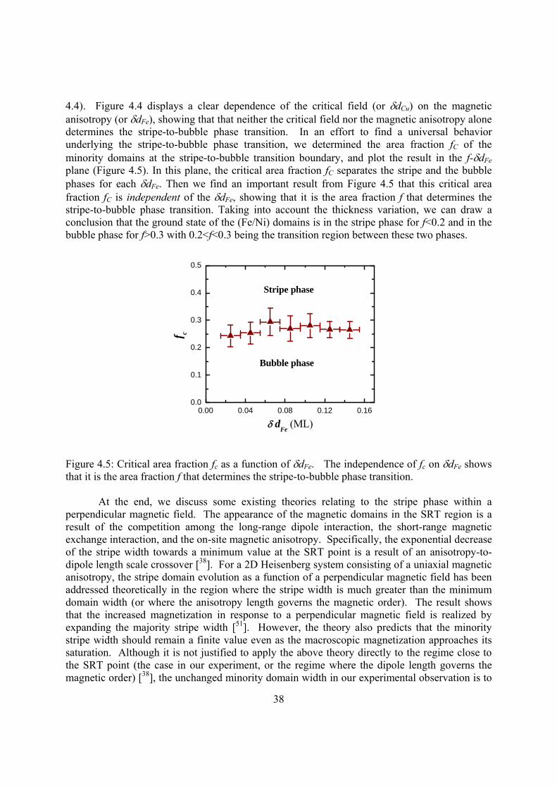
38
4.4). Figure 4.4 displays a clear dependence of the critical field (or dCu) on the magnetic anisotropy (or dFe), showing that that neither the critical field nor the magnetic anisotropy alone determines the stripe-to-bubble phase transition. In an effort to find a universal behavior underlying the stripe-to-bubble phase transition, we determined the area fraction fC of the minority domains at the stripe-to-bubble transition boundary, and plot the result in the f-dFe plane (Figure 4.5). In this plane, the critical area fraction fC separates the stripe and the bubble phases for each dFe. Then we find an important result from Figure 4.5 that this critical area fraction fC is independent of the dFe, showing that it is the area fraction f that determines the stripe-to-bubble phase transition. Taking into account the thickness variation, we can draw a conclusion that the ground state of the (Fe/Ni) domains is in the stripe phase for f<0.2 and in the bubble phase for f>0.3 with 0.2<f<0.3 being the transition region between these two phases.
0.00 0.04 0.08 0.12 0.160.0
0.1
0.2
0.3
0.4
0.5
Stripe phase
f c
dFe
(ML)
Bubble phase
Figure 4.5: Critical area fraction fc as a function of dFe. The independence of fc on dFe shows that it is the area fraction f that determines the stripe-to-bubble phase transition.
At the end, we discuss some existing theories relating to the stripe phase within a
perpendicular magnetic field. The appearance of the magnetic domains in the SRT region is a result of the competition among the long-range dipole interaction, the short-range magnetic exchange interaction, and the on-site magnetic anisotropy. Specifically, the exponential decrease of the stripe width towards a minimum value at the SRT point is a result of an anisotropy-to-dipole length scale crossover [38]. For a 2D Heisenberg system consisting of a uniaxial magnetic anisotropy, the stripe domain evolution as a function of a perpendicular magnetic field has been addressed theoretically in the region where the stripe width is much greater than the minimum domain width (or where the anisotropy length governs the magnetic order). The result shows that the increased magnetization in response to a perpendicular magnetic field is realized by expanding the majority stripe width [51]. However, the theory also predicts that the minority stripe width should remain a finite value even as the macroscopic magnetization approaches its saturation. Although it is not justified to apply the above theory directly to the regime close to the SRT point (the case in our experiment, or the regime where the dipole length governs the magnetic order) [38], the unchanged minority domain width in our experimental observation is to

39
certain degree captured by the above theory. This result was also evidenced in previous experiments although the relative poor sample quality produces a large fluctuation in the minority domain width [36, 37]. On the other hand, the appearance of the bubble domain phase reported in the present paper is certainly not included in previous theories and experiments.
Another simplified model considers only the domain wall energy and the dipole interaction energy [52]. Since both energy terms depend on specific domain patterns, the model compared the total energy of stripe phase and bubble phase within a perpendicular magnetic field. By changing the domain pattern from stripe phase into bubble phase, the increased domain wall energy due to the increased domain wall length is accompanied by a decrease of the dipole interaction energy. Thus the final domain state will depend on the competition between the above two terms. By a numerical simulation, the model shows that although the magnetization (or area fraction f) depends little on the domain patterns, the stripe- and bubble-phase energies do cross as a function of the minority area fraction, leading to a lower energy for stripe phase for f>0.28 and a lower energy for bubble phase for f<0.28. This result agrees well with our experimental observation. Ref. [52] further predicts that in the vicinity of 28.0cf , the system
should process a phase separation into a superposition of stripe and bubble domain phases in a narrow region around fc. This also agrees with our observation that the stripe and bubble domains coexist in the vicinity of the stripe-to-bubble phase transition boundary. Although this simplified model explains the appearance of the bubble domain phase within a perpendicular magnetic field, the model ignores the magnetic anisotropy term. We wish future theoretical study could be carried out to directly address our experimental observation.
4. Summary
In summary, we studied domain evolution of (Fe/Ni) film at the SRT in (Fe/Ni)/Cu/Ni/Cu(001) where the interlayer coupling simulates a virtual perpendicular magnetic field applied to the (Fe/Ni) film. We find that as the magnetic field increases, the (Fe/Ni) magnetization initially increases by increasing the majority domain area while keeping the minority stripe width unchanged, and then above a critical magnetic field the minority stripes break to evolve into a bubble domain phase. We further show that although the critical field depends on the magnetic anisotropy, a universal value of the minority domain area fraction (fC~0.2-0.3) determines the stripe-to-bubble phase transition.

40
Chapter 5 Magnetic frustration induced Ni spin switching in FeMn/Ni/Cu(001) 1. Introduction
Controlling the local electron spin direction in a magnetic nanostructure is a key step towards the spintronics technology [53]. Various methods have been proposed to reach this goal such as the spatial variation of the g-factor [54], tuning of the charge density [55], spin torque effect [ 56 , 57 ], and the voltage-controlled multiferroic antiferromagnet [ 58 ], etc. All these approaches are based to some extend on the spin-charge coupling to modify the electronic states that are coupled to the electron spins. For magnetic materials, such spin-charge coupling often manifests as the spin-orbit coupling which generates the so-called magnetic anisotropy to determine the electron spin direction. Therefore a control of the electron spin direction is ultimately related to the manipulation of the magnetic anisotropy [59, 60, 61]. Although research on the magnetic anisotropy has been greatly advanced in the last decades, the disadvantage is that once a nanostructure is synthesized the interfacial electronic states are fixed so that it is very difficult to change the magnetic anisotropy anymore. Therefore it has been highly demanded to explore new mechanisms to generate the magnetic anisotropy. In this Letter, we demonstrate a new mechanism to generate the magnetic anisotropy. We show that the spin direction of a Ni thin film in FeMn/Ni/Cu(001) could be switched from out-of-plane to in-plane direction of the film by establishing an antiferromagnetic order of the FeMn film. We attribute this result to the FeMn/Ni interfacial frustration induced magnetic anisotropy which shifts the Ni spin reorientation transition (SRT) thickness [62] by as much as 40%. We choose this system because FeMn/Ni/Cu(001) films can be grown epitaxially and that the FeMn has a well-known 3Q antiferromagnetic spin structure so that a well-defined single crystalline ultrathin films can be used for this study with the FeMn Néel temperature easily tuned by changing its film thickness [63]. 2. Experiment
A 10 mm diameter Cu(001) single crystal disk was mechanically polished down to 0.25 m diamond-paste, followed by an electropolish [64]. The substrate was cleaned in situ by cycles
of Ar+ sputtering at 2-5 keV and annealing at 600-700oC. FeMn/Ni/Cu(001) films were grown epitaxially at room temperature with the FeMn and Ni films grown into cross wedges for the purpose of controlling their thicknesses independently. A 10 ML Cu layer was grown on top of the FeMn to protect the sample from contamination. Magnetic properties of the films were measured by Magneto-Optic Kerr Effect (MOKE) and by Photoemission Electron Microscopy (PEEM) at the Advanced Light Source. The magnetic domain images were obtained by taking the ratio of L3 and L2 edges utilizing the effect of x-ray magnetic circular dichroism (XMCD) [65]. All measurements were made at room temperature.
3. Results and discussions
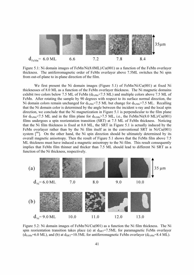
41
Figure 5.1: Ni domain images of FeMn/Ni(8.0ML)/Cu(001) as a function of the FeMn overlayer thickness. The antiferromagnetic order of FeMn overlayer above 7.5ML switches the Ni spin from out-of-plane to in-plane direction of the film.
We first present the Ni domain images (Figure 5.1) of FeMn/Ni/Cu(001) at fixed Ni thicknesses of 8.0 ML as a function of the FeMn overlayer thickness. The Ni magnetic domains exhibit two colors below 7.5 ML of FeMn (dFeMn<7.5 ML) and multiple colors above 7.5 ML of FeMn. After rotating the sample by 90 degrees with respect to its surface normal direction, the Ni domain colors remain unchanged for dFeMn<7.5 ML but change for dFeMn>7.5 ML. Recalling that the Ni domain color is determined by the angle between the incident x-ray and the local spin direction, we conclude that the Ni magnetization in Figure 5.1 is perpendicular to the film plane for dFeMn<7.5 ML and in the film plane for dFeMn>7.5 ML, i.e., the FeMn/Ni(8.0 ML)/Cu(001) films undergoes a spin reorientation transition (SRT) at 7.5 ML of FeMn thickness. Noticing that the Ni film thickness is fixed at 8.0 ML, the SRT in Figure 5.1 is actually induced by the FeMn overlayer rather than by the Ni film itself as in the conventional SRT in Ni/Cu(001) system [66]. On the other hand, the Ni spin direction should be ultimately determined by its overall magnetic anisotropy. Then the result of Figure 5.1 shows that the FeMn film above 7.5 ML thickness must have induced a magnetic anisotropy to the Ni film. This result consequently implies that FeMn film thinner and thicker than 7.5 ML should lead to different Ni SRT as a function of the Ni thickness, respectively.
Figure 5.2: Ni domain images of FeMn/Ni/Cu(001) as a function the Ni film thickness. The Ni spin reorientation transition takes place (a) at dSRT=7.5ML for paramagnetic FeMn overlayer (dFeMn=6.0 ML), and (b) at dSRT=10.5ML for antiferromagnetic FeMn overlayer (dFeMn=8.4 ML).

42
To verify this fact, we show in Figure 5.2 the Ni PEEM images as a function of the Ni film thickness at fixed FeMn thicknesses of 6.0 ML and 8.4 ML, respectively. For each case, the Ni film shows an in-plane to out-of-plane SRT with increasing the Ni thickness. However, the Ni SRT thickness of dSRT=10.5 ML in the dFeMn=8.4 ML sample is about 40% greater than the dSRT=7.5 ML value in the dFeMn=6.0 ML sample, confirming that thicker FeMn film (dFeMn>7.5 ML) induces a magnetic anisotropy which favors an in-plane alignment of the Ni spins. Since both samples have the same FeMn/Ni interface and the interfacial magnetic anisotropy depends very little on the overlayer thickness above 5ML [67], the results of Figure 5.1&2 must come from the magnetic state change of the FeMn film. Noticing that the Néel temperature of the FeMn film increases with its film thickness, we attribute the FeMn induced magnetic anisotropy to the antiferromagnetic order of the FeMn overlayer in FeMn/Ni/Cu(001) film.
Figure 5.3: The Ni SRT critical thickness dSRT as a function of dFeMn. The red solid line is guide to eyes. The antiferromagnetic order of the FeMn film above 7.5ML generates a magnetic anisotropy to increase the Ni SRT thickness from 7.5ML to 10.5 ML.
To support this conclusion, we determined the Ni SRT thickness dSRT from the PEEM
images as a function of the FeMn thickness (Figure 5.3). The thickness error from the PEEM image determination is ~0.15 ML. The dSRT remains a constant of 7.5 ML for dFeMn < 7 ML, exhibits a sudden increase for 7 ML < dFeMn <8 ML, and reaches another constant value of 10.5 ML for dFeMn > 8 ML. Then the constant Ni dSRT values for dFeMn < 7 ML and dFeMn > 8 ML correspond to the paramagnetic and antiferromagnetic states of the FeMn films. The critical thickness value of dFeMn=7.5 ML is similar to the literature value [68, 69].

43
Figure 5.4: (a) Polar MOKE hysterisis loops of FeMn/Ni/Cu(001) as a function of Ni thickness for paramagnetic FeMn overlayer (left column, dFeMn=4.3 ML), and antiferromagnetic FeMn overlayer (right column, dFeMn=8.4 ML). (b) The Ni polar remanence as a function of Ni film thickness. Arrows indicate the Ni SRT thickness. (c) The coercivity of FeMn/Ni(14.5ML)/Cu(001) as a function of the FeMn film thickness.
To further support our conclusion, MOKE measurement was taken at room temperature.
Figure 5.4(a) shows the Ni polar loops, which measure the Ni perpendicular magnetization, as a function of the Ni thickness at paramagnetic (dFeMn=4.3 ML) and antiferromagnetic (dFeMn=9.7 ML) state of the FeMn film, respectively. In both cases, the Ni film develops the polar signal above a critical thickness to eventually evolve into a square loop with a full remanence, showing the Ni SRT from in-plane to out-of-plane directions with increasing the Ni thickness. However, there are two major differences. First, the Ni SRT critical thickness is thinner at paramagnetic FeMn [left column of Figure 5.4(a)] than at antiferromagnetic FeMn [right column in Figure 5.4(a)]. This can be more clearly seen in Figure 5.4(b) where the Ni polar remanence (M⊥) is plotted as a function of the Ni thickness for dFeMn=4.3 ML and 9.7 ML, respectively. Second, it is obvious that the Ni coercivity (HC) at dFeMn=9.7 ML is much greater than at dFeMn=4.3 ML. The HC at a fixed Ni thickness of 14.5 ML shows that the Ni HC remains a constant value below 7.5 ML FeMn and then increases rapidly above 7.5 ML FeMn [Figure 5.4(c)]. The drastic increase of HC above an FeMn critical thickness is a signature of the antiferromagnetic order in the FeMn film [63]. Therefore we confirm our conclusion that it is the antiferromagnetic order of the FeMn overlayer above 7.5 ML that induces a magnetic anisotropy to the Ni film.

44
Figure 5.5: (a) the schematic drawing of 3Q-like FeMn spin structure. Arrows represent the spin orientation. Atoms are painted in three different colors to indicate different (001) planes. The dashed lines in (a) show the tetrahedral unit cell. (b) The out-of-plane and (c) in-plane FeMn spin components at a (001) island with [100] and [110] steps. The net out-of-plane spin component is non zero but alternates its direction between neighboring terraces (indicated by dot and cross at the center of atoms). The in-plane spin component has a non zero net spin only at the [100]-type step edges.
To understand why the FeMn antiferromagnetic order induces a magnetic anisotropy, we
consider the well-known 3Q-like spin structure of the face-centered-cubic (fcc) FeMn lattice [Figure 5.5(a)][70]. For FeMn (001) atomic planes, although the in-plane net spin is zero, the out-of-plane net spin is actually nonzero but alternating its direction between neighboring (001) planes. Then at the FeMn/Ni interface with the presence of atomic steps (inevitable in real experimental systems), this kind of 3Q spin structure will give rise to a nonzero perpendicular net spin at each atomic terrace whose direction alternates between neighboring terraces [Figure 5.5(b)], as well as an uncompensated in-plane spin only at the [100]-type step edges [Figure 5.5(c)][63]. For the perpendicular FeMn spin component, the FeMn/Ni magnetic coupling will then produce a magnetic frustration due to the atomic terraces [71]: the FeMn-Ni interfacial interaction favors an alternating alignment of the Ni spins between neighboring terraces while the Ni-Ni interaction prefers a parallel alignment of the Ni spins. This magnetic frustration is similar to the case of the biquadratic interlayer coupling in magnetic sandwiches [72] and the 90-degree coupling at the FM/AFM interfaces [73] where the interlayer/interfacial magnetic coupling competes with the FM intralayer coupling. The competition result is to generate a magnetic anisotropy which favors a perpendicular alignment of the FM spins to the AF spins, similar to the well-known “spin-flop” state in bulk antiferromagnets [74]. Then the FeMn/Ni out-of-plane interfacial magnetic frustration should generate a magnetic anisotropy that favors the Ni spins to be perpendicular to the FeMn out-of-plane spin direction (e.g., in-plane direction for the Ni spins). This explains why the FeMn antiferromagnetic order favors an in-plane alignment of the Ni spins. For the in-plane component of the FeMn spins, the uncompensated spins at the [±1,0,0] and [0,±1,0] step edges should create an equivalent four-fold magnetic anisotropy for the in-plane Ni magnetization [63] which could also favor an in-plane alignment of the Ni spins.

45
Figure 5.6: The Ni SRT thickness dSRT of FeMn/Ni/Cu(001) as a function of the vicinal angle for dFeMn = 5 ML and 17 ML of FeMn/Ni grown on vicinal Cu(001) with steps parallel to [100].
To differentiate the above two mechanisms, we performed an experiment using vicinal
Cu(001) substrate with the atomic steps parallel to [100] direction. The idea is that the interfacial frustration due to the FeMn out-of-plane spin component should scale linearly with the terrace area so that the magnetic anisotropy (frustration energy per unit area) should be weakly dependent on the step density [72]. On the other hand, the effect due to the in-plane FeMn uncompensated spin component at the [100]-step edges should obviously scale with the [100] step density. Therefore a study of the Ni SRT thickness as a function of the vicinal angle will distinguish these two mechanisms. A curved Cu(001) substrate is used in our experiment to change the vicinal angle ( continuously [75]. After growing a Ni wedge with its slope along the [100] step direction and covering the Ni wedge with a uniform FeMn film, MOKE measurement is carried out to determine the Ni SRT thickness dSRT. It should be mentioned that the roughness of Ni film could smear out the regular step morphology of the vicinal Cu substrate. However, our LEED measurement indicates that double LEED spots persist after the Ni film growth, indicating a well transferred step-density from the Cu substrate to the Ni/FeMn interface. Previous study on the step decoration in vicinal Ni/Cu(001) system also indicates that steps from the Cu substrate indeed persist on top of the Ni film [76]. It should also be mentioned that FeMn/Ni/Cu(001) could have a different FeMn/Ni interfacial roughness than Ni/FeMn/Cu(001) thus exhibits a different magnetic behavior [77]. Of course a final answer on the film roughness will depend on an in situ surface morphology measurement using Scanning Tunneling Microscopy. Figure 5.6 shows the result of dSRT versus the vicinal angle for paramagnetic (dFeMn=5 ML) and antiferromagnetic (dFeMn=17 ML) FeMn overlayers. The purpose of including the paramagnetic FeMn case is to identify possible effect of the step-induced magnetic anisotropy on the Ni SRT [61]. We find that for paramagnetic FeMn (dFeMn=5 ML), the dSRT value of 7.5ML is independent of , showing that we can ignore the effect of the step-induced

46
magnetic anisotropy on the Ni SRT. As the FeMn film becomes antiferromagnetic at thicker thickness (dFeMn=17 ML), the Ni dSRT value shifts from 7.5 ML to 10.5 ML, showing the effect of the FeMn/Ni interfacial frustration on the Ni SRT. More importantly, the dSRT value remains a constant of 10.5 ML rather than increases with the vicinal angle showing that the FeMn uncompensated in-plane spins at the [100]-step edges do not have an effect on the Ni SRT. Therefore the result of Figure 5.6 favors the conclusion that it is the FeMn out-of-plane spin component that is responsible for the FeMn induced magnetic anisotropy. Taking the 3 ML Ni SRT thickness shift and the Ni magnetic anisotropy value in Ni/Cu(001) system [62], we estimate the strength of this frustration induced magnetic anisotropy to be ~70 eV/spin, the same order of magnitude as estimated by Koon for an idealized frustrated interface [73]. There sometimes exists induced moment in the antiferromagnetic film at the interface when in contact with a ferromagnetic film. This indeed was observed in FeMn/Co system where both Fe and Mn XMCD signala were detected [78]. However, this induced moment is not responsible for the SRT thickness shift reported in this paper because the induced moment was observed for both paramagnetic and the antiferromagnetic phases of the FeMn film. We would like to point out that the frustration induced SRT should be a general phenomenon as far as the interfacial crystal plane of the film carries an uncompensated net spins whose direction alternates between neighboring terraces. Finally, another interesting topic for future study could be the exchange bias in this system because the unidirectional and uniaxial magnetic anisotropies due to the interfacial interaction could be separated into two directions in this system.
4. Summary
In summary, we studied the Ni spin reorientation transition in FeMn/Ni/Cu(001) system and find a 40% Ni SRT thickness shift as the FeMn overlayer transits from paramagnetic to antiferromagnetic state. We attribute this giant shift to the out-of-plane FeMn-Ni interfacial magnetic frustration which generates a magnetic anisotropy to favor an in-plane alignment of the Ni spins.
47
Chapter 6 Element-specific study of the anomalous magnetic interlayer coupling across NiO spacer layer in Co/NiO/Fe/Ag(001) using XMCD and XMLD
1. Introduction
The discovery of magnetic interlayer coupling between two ferromagnetic (FM) layers across a thin spacer layer [79] led to the discovery of the giant magneto resistance (GMR) [80] and has thereafter been stimulating a great activity in nanomagnetism research. Depending on the spacer layer material, the interlayer coupling mechanism is quite different. For metallic spacer layers, whereas the GMR effect was discovered, the interlayer coupling has been extensively studied and the oscillatory interlayer coupling [81 ] are identified to be associated with the quantum well states in the spacer layer at the Fermi level [82,83]. For insulating spacer layers, whereas the tunneling magneto resistance (TMR) [84,85] was discovered, the coupling mechanism has not been clearly understood [86 , 87 , 88 ]. In particular, the interlayer coupling across an antiferromagnetic (AF) insulating spacer layer is very ambiguous and confusing [89,90]. An anomalous 90o interlayer coupling across a thin AF NiO layer, which has become a model system for the study of this subject, was discovered in Fe3O4/NiO/Fe3O4 [
91], Ni80Fe20/NiO/Co [92], and Fe/NiO/Fe [93] systems, and it is shown that this observed 90o-coupling is different [93] from the conventional Slonczewski’s 90o-coupling in metallic systems [ 94 ]. Different and contradictious mechanisms have been proposed to account for this anomalous interlayer coupling across the NiO spacer layer. For example, the 90o-coupling was proposed to be due to a spiral rotation of the NiO spins in the spacer layer by keeping a collinear magnetic coupling at both FM/AFM interfaces [91], whereas another proposal assumes a collinear NiO spin structure but leaving the interfacial coupling to be collinear and perpendicular at the two FM/AFM interfaces, respectively [92]. Obviously, the key to resolve the coupling mechanism is a direct measurement of the NiO spin structure in the coupled magnetic sandwiches. Experimentally, this was not possible until the development of the X-ray Magnetic Linear Dichroism (XMLD) technique which could probe the AF spin direction in certain AF materials [95,96,97,98]. In fact, XMLD technique has greatly advanced our knowledge in FM/AF bilayer systems in which the so-called exchange bias effect was discovered [ 99 , 100 ]. In this Letter, we report a study of Co/NiO/Fe/Ag(001) trilayers using photoemission electron microscopy (PEEM) technique. By a direct comparison of the Co, Fe and the NiO magnetic domains, we are able to resolve the confusing issue of the anomalous interlayer coupling across the NiO spacer layer. Specifically, we find that the anomalous transition of the Co-Fe interlayer coupling from a 90o-coupling to a collinear coupling with increasing the NiO thickness is due to the fact that the NiO/Fe interfacial coupling undergoes a transition from a collinear to a 90o coupling while retaining a 90o-coupling at the Co/NiO interface. We also identified uncompensated Ni spins at the Co/NiO interface, but found no evidence of the NiO spiral spin structure. 2. Experiment A Ag(001) single crystal is prepared by Ar ion sputtering and annealing in an ultrahigh vacuum system [101]. A 15 monolayer (ML) Fe film was deposited on top of the Ag(001) substrate followed by a wedged NiO film (0-4nm) grown by a reactive deposition of Ni under an oxygen pressure of 1×10⁻⁶ Torr. Low Energy Electron Diffraction (LEED) measurement after

48
the NiO growth shows the formation of single crystalline NiO film, confirming the epitaxial growth nature of the NiO film on Fe(001) [102, 103]. Then a 2nm thick Co film was deposited onto half of the NiO wedge. This sample allows the study of both Co/NiO/Fe trilayers and NiO/Fe bilayers under the same growth condition. The absence of the LEED spots from the Co film shows the formation of polycrystalline Co film. The sample is covered by a 2nm protection Ag film before bringing it to the PEEM-II station at the Advanced Light Source (ALS) of the Lawrence Berkeley National Laboratory. As reported in the literature, Fe film grown on Ag(001) has a bcc structure with the Fe [100] axis parallel to the Ag [110] axis and the NiO film on Fe(001) has an fcc structure with the NiO [110] axis parallel to the Fe [100] axis [104]. To avoid confusion, all the crystalline axes in this paper are specified according to the bcc Fe unless otherwise specified. 3. Results and discussions
Figure 6.1: Co and Fe magnetic domains as a function of NiO thickness from Co(2nm)/NiO/Fe(15ML)/Ag(001). The correspondence between domain contrast and spin orientation is shown in the schematic drawing as a reference. Arrows represent the spin orientations. The result shows that the Co and Fe have a 90o-coupling for dNiO<2.0 nm and a collinear coupling for dNiO>2.0 nm. We first present the result of magnetic interlayer coupling between Co and Fe films. The ferromagnetic Co and Fe domains (Figure 6.1) are obtained by taking the ratio of the corresponding Co and Fe L3 and L2 absorption edges with circular polarized incident x-rays [105]. In our measurement, the x-ray is in the (100) plane and makes an incident angle of 60o with respect to the surface normal direction ([001] direction). Since the XMCD signal is determined by the projection of the ferromagnetic spin to the incident x-ray direction, the ferromagnetic spin orientation (arrow symbols in Figure 6.1) can be determined from the domain contrast with the white, dark, and grey domains corresponding to spins parallel to [010], [0-10], and [±100] axis, respectively (see the schematic drawing in Figure 6.1). After assigning the spin direction to the Fe and Co domains, we immediately identified that the Fe and Co spins are coupled perpendicularly to each other (90o-coupling) for NiO thickness thinner than ~2nm (dNiO<2 nm), and collinearly for dNiO>2 nm. It should be mentioned that below 1ML NiO, we observed a ferromagnetic interlayer coupling between the Fe and Co films which is not surprising because the Fe and Co films should be partially connected under this condition. Note that Slonczewski’s

49
90o-coupling comes from interfacial roughness, thus can not explain our observation because it would lead to a 90o-coupling at thicker NiO film where a rougher NiO film is expected. Another observation is that there co-exist both “FM-coupling” and “AF-coupling” in the collinear coupling regime (dNiO>2.0 nm). As it will be explained later, this coexistence is not due to inhomogeneity of the sample but is energetically degenerate due to 90o-coupling at both Co/NiO and NiO/Fe interfaces.
Figure 6.2: Normalized energy spectra from the Ni L2 edge of NiO for two orthogonal linear polarizations. The inset shows the sinusoidal dependence of the L2 ration as a function of the polarization angle . We then studied the NiO AF spin structure to identify its role in the Co-Fe interlayer coupling. We took the Ni L2 energy spectra from NiO(3.0nm)/Fe/Ag(001) to identify the existence of the X-ray Magnetic Linear Dichorism (XMLD) effect. An external magnetic field is applied to align the Fe spin parallel to the [010] axis, and two energy spectra were taken with the
x-ray linear polarization vector E
parallel (=0o) and perpendicular (=90o) to the Fe spin direction (Figure 6.2). The spectra are normalized by the peak intensity at the lower peak energy of 870.3 eV for a clear view of the difference in the two spectra. The L2 ratio [defined as RL2=I(870.3 eV)/I(871.3 eV), where I is the normalized intensity.], which is a direct measure of the XMLD effect, is plotted in the inset as a function of the x-ray polarization angle. The L2 ratio has a sinusoidal dependence on the polarization angle with the minimum and maximum values being at =0o and =90o, respectively, showing that the NiO spin direction is in the NiO [±110] direction. As shown by previous works [106,107], for easy axis in the NiO [±110] direction the L2 ration of NiO should reach its maximum value as the NiO spin is parallel to the x-ray polarization direction. Therefore the result of Figure 6.2 shows that the NiO spins in the dNiO=3.0 nm sample are parallel to the Fe[100] axis, i.e., orthogonal to the Fe spin direction.
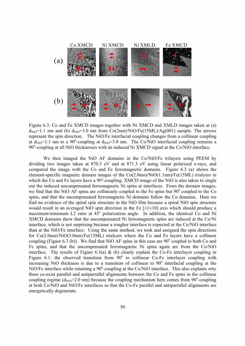
50
Figure 6.3: Co and Fe XMCD images together with Ni XMCD and XMLD images taken at (a) dNiO=1.1 nm and (b) dNiO=3.0 nm from Co(2nm)/NiO/Fe(15ML)/Ag(001) sample. The arrows represent the spin direction. The NiO/Fe interfacial coupling changes from a collinear coupling at dNiO=1.1 nm to a 90o-coupling at dNiO=3.0 nm. The Co/NiO interfacial coupling remains a 90o-coupling at all NiO thicknesses with an induced Ni XMCD signal at the Co/NiO interface.
We then imaged the NiO AF domains in the Co/NiO/Fe trilayers using PEEM by dividing two images taken at 870.3 eV and at 871.3 eV using linear polarized x-rays, and compared the image with the Co and Fe ferromagnetic domains. Figure 6.3 (a) shows the element-specific magnetic domain images of the Co(2.0nm)/NiO(1.1nm)/Fe(15ML) trialyers in which the Co and Fe layers have a 90o-coupling. XMCD image of the NiO is also taken to single out the induced uncompensated ferromagnetic Ni spins at interfaces. From the domain images, we find that the NiO AF spins are collinearly coupled to the Fe spins but 90o coupled to the Co spins, and that the uncompensated ferromagnetic Ni domains follow the Co domains. Here we find no evidence of the spiral spin structure in the NiO film because a spiral NiO spin structure would result in an averaged NiO spin direction in the Fe [±1±10] axis which should produce a maximum/minimum L2 ratio at 45o polarization angle. In addition, the identical Co and Ni XMCD domains show that the uncompensated Ni ferromagnetic spins are induced at the Co/Ni interface, which is not surprising because a rougher interface is expected at the Co/NiO interface than at the NiO/Fe interface. Using the same method, we took and assigned the spin directions for Co(2.0nm)/NiO(3.0nm)/Fe(15ML) trialyers where the Co and Fe layers have a collinear coupling (Figure 6.3 (b)). We find that NiO AF spins in this case are 90o coupled to both Co and Fe spins, and that the uncompensated ferromagnetic Ni spins again are from the Co/NiO interface. The results of Figure 6.3(a) & (b) clearly explain the Co-Fe interlayer coupling in Figure 6.1: the observed transition from 90o to collinear Co-Fe interlayer coupling with increasing NiO thickness is due to a transition of collinear to 90o interfacial coupling at the NiO/Fe interface while retaining a 90o-coupling at the Co/NiO interface. This also explains why there co-exist parallel and antiparrallel alignments between the Co and Fe spins in the collinear coupling regime (dNiO>2.0 nm) because the coupling mechanism here comes from 90o-coupling at both Co/NiO and NiO/Fe interfaces so that the Co-Fe parallel and antiparrallel alignments are energetically degenerate.

51
Figure 6.4: Fe XMCD image together with Ni XMCD and XMLD images taken at (a) dNiO=1.1 nm and (b) dNiO=3.0 nm from of NiO/Fe(15ML)/Ag(001). The arrows represent the spin directions. The NiO/Fe interfacial coupling changes from a collinear coupling at dNiO=1.1 nm to a 90o-coupling at dNiO=3.0 nm. No induced Ni XMCD signal is detected.
Theoretically, a 90o-coupling is expected at the FM/AFM interface for a perfect
compensated AFM interface [108]. It is suggested that uncompensated spins of the AF layer due to roughness and defects could induce different types of interfacial coupling [105, 109, 110]. Since an increase of the NiO thickness in Co/NiO/Fe/Ag(001) is likely to change the roughness at the Co/NiO interface rather than at the NiO/Fe interface, it is quite interesting that we observe a 90o-coupling and uncompensated Ni spins at the Co/NiO interface for all NiO thicknesses, but both a collinear coupling (dNiO<2.0 nm) and a 90o-coupling (dNiO>2.0 nm) at the NiO/Fe interface. It should be pointed out that the measured Ni XMCD signal could in principle come from both the Co/NiO and NiO/Fe interfaces. To further separate the contributions from the NiO/Fe interface, we performed XMCD and XMLD measurement on NiO/Fe(15ML)/Ag(001) bilayers. We observe the collinear to 90o coupling switching with increasing NiO thickness in the bilayer system (Figure 6.4), consistent with the result reported before [104]. More importantly, no Ni XMCD signal is detected for all NiO thicknesses, suggesting that the all the uncompensated Ni spins in Co/NiO/Fe sandwich come from the Co/NiO interface. We are unclear, however, on whether the observed uncompensated Ni signal at the Co/NiO signal is responsible for the different Co/NiO and NiO/Fe interfacial magnetic couplings. Further investigation is needed to clarify this issue.
4. Summary
In summary, the Co-Fe magnetic interlayer coupling in Co/NiO/Fe/Ag(001) trilayers switches from a 90o-coupling to a collinear coupling with increasing the NiO thickness. This anomalous coupling is due to a switching of the NiO/Fe interfacial coupling from a collinear to a 90o-coupling with increasing the NiO thickness while retaining a 90o-coupling at the Co/NiO interface. Induced uncompensated Ni spins are observed at the Co/NiO interface, but not at the NiO/Fe interface. No evidence of spiral NiO spin structure is found in this system.

52
Chapter 7 Tailoring exchange bias by oxidizing Co film across a Cu wedge in Cu(wedge)/CoO/Co/Cu(001)
1. Introduction
Meiklejohn and Bean discovered that as partially oxidized Co particles are cooled to below the antiferromagnetic (AFM) CoO Néel temperature (TN) within a magnetic field, the magnetic hysteresis loop of the ferromagnetic (FM) Co core is shifted along the magnetic field axis [111]. This phenomenon is referred to as exchange bias. Understanding the mechanism of the exchange bias and developing new methods of controlling the exchange bias have been an active research field in the last few decades because of its importance in device applications [112]. Both nanoparticles and thin films have been applied to study the exchange bias in FM/AF systems. It is found that the exchange bias crucially depends on the AF order and the AF microstructure [113]. Among many AF materials, CoO has become one model system because of its structural and magnetic simplicity, as well as its profound effect on the magnetic properties of the FM layers, such as the magnetic anisotropy [114]. Recently there has been a great effort made on how to control the CoO oxidation process in order to tailor the exchange bias systematically. For example, Au/Co/Au nanopillars were fabricated by lithography to manipulate the coercivity and exchange bias of the resulting CoO/Co system [115]. Modifying the oxygen content in CoO/Co nanoparticles was also applied to control the exchange bias [116]. The CoO oxide layer is usually created either by annealing the Co within an oxygen environment or by growing the Co in an oxygen environment. In either method it is difficult to control and reproduce the same oxidation conditions, thus making it difficult to systematically vary the exchange bias. To fully develop the application potential of the exchange bias, it is highly demanded to develop a new method that could control the CoO oxidation so that it is possible to tailor the exchange bias systematically. In this paper, we report a new method of controlling the CoO oxidation by annealing a Cu-covered Co film in an oxygen environment. By growing the Cu overlayer into a wedge shape, we are able to control the Co underlayer oxidation continuously as a function of the Cu layer thickness. As a result we are able to tailor the exchange bias of the CoO/Co film systematically. 2. Experiment
The sample was prepared in an Ultra High Vacuum (UHV) system with a base pressure of 2×10⁻¹⁰ Torr. A Cu(001) single crystal substrate was mechanically polished down to 0.25m diamond paste followed by an electropolishing [117]. The substrate was cleaned in the UHV chamber by cycles of 1-2 keV Ar ion sputtering and annealing at 600oC. Auger Electron Spectroscopy (AES) and Low Energy Electron Diffraction (LEED) were used to characterize the sample. A 10 monolayer (ML) Co film was grown onto the Cu(001) substrate epitaxially at room substrate temperature. Then a Cu wedge (0-2 nm) was grown on top of the Co film by moving the substrate behind a knife-edge shutter during the Cu evaporation. The slope of the wedge (10 Å /mm) is controlled by the moving speed of the substrate and the Cu evaporation rate which was calibrated by a thickness monitor. LEED pattern shows that high quality single crystalline Cu and Co films are obtained under this condition (Figure 7.1). The sample was then

53
annealed at 200oC in an oxygen environment of 10-6 Torr to oxidize the Co film under the Cu wedge.
3. Results and discussions
Figure 7.1: LEED patterns taken at ~130 eV before and after oxidation. The presence of the LEED pattern after the oxidation shows that the Co film retains its single crystalline structure.
LEED and Auger measurements were performed after the sample growth. Figure 7.1 shows the LEED patterns after the oxidation (LEED pattern before the oxidation is also shown as a reference). Without the Cu capping layer, the oxidized Co surface exhibits a 1×1 LEED pattern with slightly broadened diffraction spots as compared to a clean surface. With the Cu capping layer, the LEED pattern after the oxidation exhibits the well-known (2√2×√2)R45° structure which corresponds to the disassociate O/Cu(001) surface [118]. In literature, a c(2x2)-O/Cu(001) structure was also reported under specific conditions [119] but is not present in our film. Since the reconstruction of the O/Cu(001) surface is irrelevant to the exchange bias of the CoO/Co system, we would not discuss it here. Nevertheless, the presence of the LEED diffraction after the oxidation indicates that the Co underlayer retains its single crystalline structure.

54
Figure 7.2: Cu, Co, and O AES peak intensities as a function of the Cu wedge thickness. The similar behavior of the Co and O AES peaks indicates the formation of CoO under Cu capping layer.
AES was then measured across the Cu wedge for the O, Co, and the Cu peaks (Figure
7.2). As expected, the Cu AES peak increases with the Cu capping layer thickness. In contrast, the Co AES peak decreases with the Cu thickness because of the finite escaping path of the Co Auger electrons in the Cu capping layer. The interesting observation is that the O AES peak also decreases with the Cu thickness in a similar manner as the Co peak. This result shows that oxygen is not only present at the Cu surface but also from the Co film below the Cu layer, a strong evidence of the CoO formation under the Cu capping layer. The decreased oxygen AES peak intensity with increasing the Cu thickness then suggests that the Cu wedge indeed controls the amount of CoO formation with thicker Cu layer leading to a thinner CoO layer. Theoretically, the AES peak intensity is determined by the AES electrons escaped from the film at different depth. Thus in principle if the escaping depth of electrons in Cu, CoO, and Co can be accurately determined, it is possible to determine the amount of oxygen as a function of Cu thickness by adding the AES contribution from each monolayer of signal with the corresponding attenuation. Such analysis has been exercised in magnetic dichroism analysis [120]. In our experiment, however, such analysis is impractical because of the lack of knowledge on the electron escaping depth in Cu, CoO, and Co as well as the instrumental limitation of our AES apparatus. All these limitations won’t allow us to determine the CoO portion with monolayer accuracy. However, as shown in the next section, we can actually determine the CoO amount in a much accurate way using magnetic measurement. Therefore we here present the AES data only as supporting evidence that the oxygen indeed penetrates the Cu layer to oxidize the Co film.
Figure 7.3: MOKE magnetic hysterisis loops at different Cu capping layer thicknesses after the oxidation.
The sample was cooled down to T~120K within a 350 Oe magnetic field along the Co
[110] easy magnetization axis, and measured by Magneto-Optic Kerr Effect (MOKE). A p-polarized He-Ne laser beam was reflected by the sample surface, and passes through an

55
analyzing polarizer set at ~2o from extinction. A quarter-wave plate was used to remove the birefringence of the UHV window. The light intensity, referred to as the Kerr intensity, is then detected by a photodiode and recorded as a function of the applied magnetic field H to generate the hysteresis loop. H was applied in the film plane and in the plane of the incident light (longitudinal Kerr effect) so that the measured hysteresis loops are from the in-plane magnetization. The Kerr effect of a ferromagnetic film rotates the polarization plane of the incident beam after reflection, leading to a non-zero small s-component of the electrical field ES of the reflected beam in addition to the dominant p-component EP (|ES| << |EP|). We define the complex Kerr rotation ES/EP =' + i", where ' and " are called the Kerr rotation and ellipticity, respectively. In our experimental arrangement the quarter-wave plate produces a 90° phase so that the measured Kerr intensity is:
I = i Ep sin + ES cos 2 Ep
2 - i ' + " 2
Ep 2 ( 2
+ 2 " ) = I0 ( 1 + 2 "/ ) (1), where I0=|EP|2 is the Kerr intensity at zero net magnetization. Thus, the peak-to-peak
intensity I, which is the difference between the Kerr intensity at positive and negative saturation field, yields the Kerr ellipticity.
" = 4
II0
. (2)
The magnitude of the Kerr ellipticity depends on refraction index, incident angle, and the Vort vector of the Co material, etc. In the thin limit that the film thickness is much less than the light wavelength, the so-called additivity law states that the Kerr rotation and ellipticity are proportional linearly to the ferromagnetic film thickness [121]. Therefore a measurement of the Kerr ellipticity magnitude would allow a determination of the ferromagnetic Co proportion after the film’s oxidation.

56
Figure 7.4: Kerr ellipticity normalized at 10 ML Co as a function of Cu capping layer thickness. The normalized Kerr ellipticity represents the amount of ferromagnetic Co in Cu/CoO/Co/Cu(001). Solid line is a fitting result using a phenomenological formula (see text).
Figure 7.3 shows representative hysteresis loops of the films at different Cu thicknesses
after the oxidation. Thinner than ~0.5 nm of Cu, we did not observe hysteresis loops, showing that the 10 ML Co is fully oxidized for Cu thinner than 0.5 nm, i.e., there is no ferromagnetic Co left under this condition. Thicker than 0.5 nm of Cu, the Co hysteresis loop develops into a well-defined square loop, showing that some Co retains its ferromagnetic state after oxidation. This result proves that the Cu wedge controls the oxidation of the Co underlayer with less CoO formation at thicker Cu thickness. The Kerr ellipticity of the CoO/Co film normalized by the Kerr ellipticity at 10ML Co [”(CoO/Co)/”(10MLCo)] thus represents the ferromagnetic Co signal in the oxidized Cu/CoO/Co/Cu(001) film. The result can be well fitted using a phenomenological formula of
0exp1)10("/)/("
ddMLCoCoCoO (3).
The fitting result yields 0d 0.35 nm and 0.29 nm. Note that the Co film is fixed at
10 ML before oxidation regardless of the Cu overlayer thickness and that AF CoO does not contribute to the MOKE signal, the result of Figure 7.4 actually represents the fact that CoO layer thickness decreases exponentially with the Cu overlayer thickness with 0.29 nm being the effective Cu thickness to protect the Co underlayer from the oxidation. Figure 7.3 also shows that the coercivity the Co film after oxidation increases as compared to a pure Co film. Noticing that the CoO layer on top of the Co film should not only generates an exchange bias but also a coercivity enhancement [112], the coercivity increase in Figure 7.3 further supports the AES and MOKE results that the Co film has been partially oxidized under the Cu wedge.
Figure 7.5: The exchange bias (HE) and the coercivity (HC) as a function of the Cu capping layer thickness. The result shows that the Cu capping wedge thickness controls the exchange bias of

57
the CoO/Co underlayer systematically. In the inset, HE ×dCo is calculated to examine the dependence of exchange bias on ferromagnetic Co thickness.
The exchange bias field (HE) of the Cu/CoO/Co/Cu(001) film is determined from the
MOKE hysteresis loop by averaging the positive and negative coercive fields. The result (Figure 7.5) shows that HE reaches a maximum value of ~170 Oe at ~0.6 nm of Cu, right after ferromagnetic Co signal is detected by MOKE, and then decreases monotonically to ~50 Oe at ~1.6 nm of Cu. Generally speaking, the exchange bias depends on the FM and AF layer thicknesses. In the extreme limit that the spin pinning is totally localized at the FM/AFM interface, the HE value should be inversely proportional to the FM layer thickness as in the Malozemoff’s model [ 122 ]. To test this relationship, we plot the product of ”(CoO/Co)/”(10MLCo), which is proportional to the ferromagnetic Co thickness (dCo) in the CoO/Co film, and the exchange bias HE as a function of the Cu thickness (inset of Figure 7.5). The non-constant value of dCo·HE shows that the exchange bias is NOT inversely proportional to the FM layer thickness. In fact, recent measurements on the training effect [123] and on the depth profile of the FM spins [ 124 ] all show that the Malozemoff’s model is over simplified in describing the exchange bias quantitatively. Nevertheless, the continuous decrease of the exchange bias with the Cu thickness demonstrates the fact that the Cu capping wedge controls and tailors the exchange bias of the CoO/Co underlayer systematically.
4. Summary
In summary, we demonstrated that a Cu wedge in Cu(wedge)/Co(10ML)/Cu(001) film controls the amount of the oxidation of the Co underlayer in a systematic manner. This method overcomes the difficulty of controlling the annealing time and oxygen pressure during the Co oxidation process. Our result shows that the Cu(wedge)/CoO/Co/Cu(001) film exhibits a continuous change of the exchange bias as a function of the Cu wedge thickness, thus offering a new method in controlling the exchange bias of CoO/Co thin films.

58
Chapter 8 A direct measurement of rotatable and frozen CoO spins in exchange bias system of CoO/Fe/Ag(001)
1. Introduction
As a ferromagnetic(FM)/antiferromagnetic(AFM) system is cooled down within a magnetic field to below the Néel temperature (TN) of the AFM material, the shift of the FM hysteresis loop in the applied magnetic field is referred to as exchange bias [125]. Investigation of exchange bias has been one of the most active areas in nanomagnetism research because of its importance to spintronics technology, especially to the design of spin valves [126]. While it is well accepted that AFM order in a FM/AFM system is responsible for the exchange bias [127,128], it remains a mystery on how the AFM spins behave during the FM magnetization reversal. Consequently, different AFM spin structures have been proposed to explain the exchange bias [129,130,131,132]. Most measurements are based on the FM layer hysteresis loops which explore only indirectly the AFM spin behavior during the FM magnetization reversal, such as in the study of training effect [133,134,135], pinning orientation effect [136,137,138,139], and finite size effect [140,141], etc. Recently, the development of X-ray Magnetic Circular Dichroism (XMCD) and X-ray Magnetic Linear Dichroism (XMLD) [142] allows an element-specific study of the FM/AFM systems. The result shows clearly a correlation between the FM and the AFM domains, and the existence of a small amount of uncompensated spins in the AFM layer [ 143 ]. These uncompensated spins in the AFM layer were consequently used to probe the AFM spin behaviors during the magnetization reversal. The result shows that only a small percentage of the uncompensated spins is pinned to account for the exchange bias [144,145,146,147]. Moreover, the pinned uncompensated AFM spins actually extend into the AFM layer [148], suggesting a bulk-like effect of the AFM spins in generating the exchange bias. In fact, an alternative approach by doping the AFM layer with non-magnetic elements [ 149 , 150 , 151 , 152 ,] and by studying a FM/AFM/FM trilayer also show a bulk effect of the AFM layer in the exchange bias [153]. Despite the above summarized progress, the compensated AFM spin behavior remains unclear during the FM layer reversal in exchange bias systems. It is usually assumed that the AFM compensated spins in a FM/AFM system should be frozen, i.e. their orientation fixed to the lattice to generate an exchange bias. However, one direct measurement on Co/bulk NiO(001) shows that the NiO spins at the Co/NiO interface may exhibit a spring-like winding structure during the Co magnetization alignment [154]. This result raises a critical issue, i.e. whether it is necessary to freeze the majority of the AFM compensated spins to generate an exchange bias in a FM/AFM thin film system. Unfortunately, this question has never been addressed directly in an experiment. A clarification of this issue obviously requires a direct measurement of the AFM compensated spins during the FM magnetization reversal. XMLD is currently the only available technique to make such a measurement. However, unlike XMCD, which can be applied to almost any types of FM thin films, XMLD can be applied only to a few types of single crystalline AFM films. That is probably why only Co/bulk NiO(001) has been measured so far on the response of the AFM spins to an applied magnetic field in exchange biased systems. In this Letter, we report an experimental study of CoO/Fe/Ag(001) single crystalline thin films. Using XMLD measurements within a magnetic field parallel and perpendicular to the field cooling direction, we are able to separate for the first time the rotatable and frozen compensated

59
CoO spins during the Fe magnetization reversal. We find the remarkable result that as the CoO thickness increases, the exchange bias is well established before frozen spins are detected in CoO film. Using a 2ML NiO as a probe layer, we further show that the rotatable and frozen CoO spins are uniformly distributed in the CoO film, suggesting that the exchange bias is determined by the bulk spin structure of the CoO film.
2. Experiment
A Ag(001) single crystal substrate was prepared in an ultra-high vacuum system by cycles of Ar ion sputtering at ~2keV and annealing at 600oC. A 15 monolayer (ML) Fe film was grown on top of the Ag(001) substrate. Then a CoO wedge (0-8 nm) was on top of the Fe film by a reactive deposition of Co under an oxygen pressure of 1×10⁻⁶ Torr. Low Energy Electron Diffraction (LEED) shows well-defined diffraction spots, indicating the formation of epitaxial single crystalline CoO film which agrees with the literature result [155]. The sample is covered by a 2nm Ag protection layer and then measured at beamlines 4.0.2 and 11.0.1 of the Advanced Light Source (ALS) of the Lawrence Berkeley National Laboratory. As reported in the literature, Fe film on Ag(001) has a bcc structure with the Fe [001] axis parallel to the Ag [110] axis and CoO film on Fe(001) has an fcc structure with the CoO [110] axis parallel to the Fe [100] axis.
3. Results and discussions
Figure 8.1: (a) X-ray Absorption Spectra (XAS) of Co L3 edge taken at two orthogonal linear polarizations (=0o and 90o) for CoO(6.0 nm)/Fe(15 ML)/Ag(001). The asymmetry of two spectra represents XMLD signal. (b) Magnetic domain images of ferromagnetic Fe and antiferromagnetic CoO taken by XMCD and XMLD, respectively. Arrows indicate the orientation of Fe and CoO spins. It is clear that the antiferromagnetic CoO spins are 90o coupled to Fe spins.

60
XMLD effect is clearly seen by measuring the X-ray absorption spectrum (XAS) at the CoO L3 edge (Figure 8.1(a)) with different X-ray polarization directions at the normal incidence. The L3 ratio (RL3), defined as the ratio of the XAS intensity at 778.1 eV and at 778.9 eV (the lower energy intensity divided by the higher energy intensity), is used to quantify the XMLD effect [156]. For element-specific domain imaging, the sample of CoO(6 nm)/Fe(15 ML)/Ag(001) was cooled to 90 K and measured by PEEM-3 with the incident x-ray at 60o incident angle and circularly polarized for Fe domain imaging, and linearly polarized (parallel to the horizontal axis of the PEEM image in Figure 8.1(b)) for CoO domain imaging. We find that the CoO domains follow exactly the Fe domains (Figure 8.1(b)), showing that the Fe magnetization aligns the AFM CoO spin axis. Noting that Fe [100] axis is parallel to CoO [110] axis, the L3 ratio analysis [156,157,158] then leads to the conclusion that the in-plane CoO AFM spins have a 90o-coupling to the Fe spins in the CoO(6 nm)/Fe(15ML)/Ag(001) sample.
Figure 8.2: Hysteresis loops of ferromagnetic Fe and antiferromagnetic CoO for CoO/Fe(15 ML)/Ag(001) taken by XMCD and XMLD, respectively. Arrows indicate the ramping direction of magnetic field. The presence and absence of the CoO response to the magnetic field at dCoO=2.0 nm and at dCoO=6.0 nm show rotatable and frozen compensated spins in the 2.0 nm and 6.0 nm thick CoO films respectively.
For the spectroscopy measurement, the sample was cooled down to 90 K within a 4 kOe
magnetic field along the Fe [100] crystal axis. Element-specific Fe and CoO hysteresis loops are measured at 90 K with the applied field in the field cooling direction. A small transverse in-plane field was applied during the hysteresis loop measurement to ensure a rotational Fe magnetization reversal. In the XMLD measurement of the CoO L3 edge, the x-ray polarization direction is also parallel to the field cooling direction. Figure 8.2 depicts representative hysteresis loops of CoO/Fe(15 ML)/Ag(001) at two different CoO thicknesses. While the Fe film exhibits expected square shape hysteresis loop, the most interesting observation is the appearance of the CoO XMLD hysteresis loop (Figure 8.2) in dCoO=2.0 nm sample. No XMCD

61
is observed at the Co L3, L2 edges so that the Co XMLD signal represents the CoO compensated spins. The presence of the CoO hysteresis loop shows clearly that the CoO compensated spins rotate during the Fe magnetization reversal: as the Fe magnetization is saturated in the positive and negative field directions, the CoO spins have the same spin axis to give the same XMLD signal; as the Fe magnetization rotates by 90o at the Fe coercive field, the CoO spins also rotate by 90o to give a maximum (peak) XMLD signal. In contrast, the absence of the CoO hysteresis loop in dCoO=6.0 nm sample shows that the CoO spins are totally frozen during the Fe magnetization reversal. It is worth pointing out that our result is different from the Co/bulk NiO(001) result which shows a non zero response of the NiO spins in the interfacial region to the external magnetic field [154]. We attribute this difference to the different NiO and CoO magnetic properties, i.e. the fact that CoO exhibits a much stronger magnetic anisotropy than NiO.
Figure 8.3: Fe film coercivity (HC), exchange bias (HE) and the percentage of CoO frozen spins in CoO/Fe(15ML)/Ag(001) as a function of CoO thickness. The remarkable fact is that HE develops below 2.2 nm CoO thickness where no frozen CoO spins are detectable. The solid lines are guides to eyes.
We then present the result of Fe hysteresis loops as a function of the CoO thickness.
Figure 8.3 shows the Fe film coercivity (HC) and exchange bias (HE) as a function of the CoO thickness. As expected, the HC and HE increases with CoO thickness and saturate at thicker CoO thickness. However, while the HC starts to increase at dCoO~0.2 nm, the HE develops only above a critical thickness of dCoO=0.8 nm. The increase of the HC is due to the establishment of the AFM order of the CoO layer [126] and this is confirmed by our observation of non-zero XMLD signal above dCoO=0.2 nm. Then the onset of HE at dCoO=0.8 nm shows that the exchange bias does not develop right after the CoO establishes its AFM order. Recognizing the rotatable and frozen CoO spins at thinner and thicker CoO thicknesses (Figure 8.2), it is tempting to associate the onset of the exchange bias to the onset of the frozen spins in the CoO layer. There has been no direct measurement so far to quantitatively single out the amount of frozen spins in the AFM layer. We carried out the following measurement to separate the rotatable and frozen spins in the CoO layer. We performed XMLD measurement as a function of the polarization angle () to

62
obtain the -dependence of the L3 ratio RL3. The RL3 angular dependence for fixed spin orientation can be approximately described by RL3cos2with the coefficient A proportional to the amount of the AFM compensated spins. Therefore a RL3- measurement allows the determination of the amount of AFM spins under specific conditions.
Figure 8.4: Polarization angle dependence of the Co L3 ratio measured with a 0.4 Tesla in-plane magnetic field at different CoO thicknesses in CoO/Fe(15 ML)/Ag(001). Solid lines are fitting results of cos2-dependence. The L3 ratio differenceRL3=RL3(90o)-RL3(0
o) is proportional to the sum and subtraction of the frozen and rotatable CoO spins for field parallel (top row) and perpendicular (lower row) to the field cooling direction, respectively.
We first measured the RL3- dependence right after the field cooling. Under this
condition, both rotatable and frozen CoO spins should be aligned to the same direction so that the RL3 difference at =90o and =0o [e.g., RL3=RL3(90o)-RL3(0
o)] is proportional to the total CoO spins. The result (top row of Figure 8.4) shows that RL3 (offset at =45o and normalized by CoO thickness) indeed follows a cos2 dependence on the polarization angle. We then rotate the in-plane magnetic field by 90o (perpendicular to the field-cooling direction) to rotate the Fe magnetization by 90o in the film plane. Under this condition, the rotatable CoO spins should follow the Fe magnetization to rotate by 90o while the frozen CoO spins should remain in their original direction, leading to a reduction of the L3 ratio. Then RL3 in this case should correspond to the subtraction of the frozen spins and the rotatable spins inside the CoO film. The result (lower row of Figure 8.4) indeed shows a thickness dependent RL3. At dCoO=6.0 nm, the RL3- dependence remains unchanged after the field rotates by 90o, showing that there is no rotatable spins at this thickness. As the CoO thickness decreases to dCoO=2.5 nm, RL3 decreases (lower row of Figure 8.4), showing that some CoO spins rotate away from the field cooling direction in the CoO film. Thinner than dCoO=2.5nm, RL3 reverses its sign, showing that there are more rotatable spins than frozen spins in the CoO film. It should be mentioned that RL3 always reaches its maximum/minimum value at =0o or =90o. This behavior rules out the spring-like (or domain wall like) spin structure normal to the CoO film because a spring-like spin structure should lead to a maximum/minimum value of the L3 ratio at an angle between =0o and

63
=90o (in an extreme case of a perfect 90o domain wall structure, the L3 ratio should reach its maximum/minimum value at =45o). The difference of RL3 for field parallel and perpendicular to the field cooling direction allows us to determine quantitatively the percentage of the frozen spins in the CoO film. Figure 8.3 shows the result of the frozen CoO spins as a function of CoO film thickness. The CoO film has no detectable frozen spins below 2.2 nm (with an error bar of ~0.1 nm), becomes partially frozen for 2.2 nm<dCoO<4.5 nm, and has all spins frozen for dCoO>4.5 nm. We then find the remarkable result that the exchange bias develops even when no frozen CoO spins are detectable at dCoO<2.2 nm, reaches ~2/3 of its saturation value at the onset of the frozen spins at dCoO=2.2 nm, and becomes saturated at dCoO=3 nm where 80% of the CoO spins are frozen. This result is contrary to the general concept that majority of AFM spins should be frozen to generate an exchange bias in a FM/AFM system. We estimate an upper limit of no more than ~5% (~0.1nm) of frozen spins below dCoO=2.2 nm. Therefore we conclude that ~5% frozen CoO spins should be enough to generate an exchange bias in CoO/Fe/Ag(001) system. This result may explain why only a small percentage of pinned uncompensated spins would be enough to account for the exchange bias [144-148].
Figure 8.5: A 2 ML NiO layer is inserted on the top or bottom of CoO to detect the depth-dependent distribution of the frozen CoO spins. The same thickness dependences of the frozen CoO and NiO spins indicate a uniform distribution of the frozen spins in the CoO film.
The next question is where the rotatable and frozen CoO spins are located? To answer
this question, we inserted a 2 ML NiO probe layer at the CoO/Fe interface and at the surface of CoO/Fe by growing two samples of CoO(wedge)/NiO(2 ML)/Fe(15 ML)/Ag(001) and NiO(2 ML)/CoO(wedge)/Fe(15 ML)/Ag(001), and measured the Ni XMLD as a function of the CoO thickness. The result shows that the NiO XMLD follows exactly the CoO thickness dependence, no matter the NiO is at the CoO/Fe interface or at the Co/Fe surface (Figure 8.5). This result shows that the rotatable and frozen spins distribute uniformly inside the entire CoO film, supporting the doping and FM/AFM/FM results [149-153] that the exchange bias depends on the bulk AFM spin structure rather than the AFM spins at the FM/AFM interface only.

64
4. Summary In summary, we investigated epitaxially grown CoO/Fe/Ag(001). Using element-specific
XMLD measurement, we separate rotatable and frozen spins in antiferromagnetic CoO film. We find that the CoO spins are rotatable below 2.2 nm CoO thickness, become partially frozen between 2.2 nm and 4.5 nm, and totally frozen above 4.5 nm. Contrary to the expectation, the exchange bias of the Fe film develops at dCo>0.8 nm even when no frozen spins are detectable in CoO film, reaches ~2/3 of its saturation value at the onset of frozen CoO spins at dCo=2.2 nm, and saturates at dCoO=3 nm where 80% of the CoO spins are frozen. With the XMLD sensitivity estimation, we conclude that ~5% of frozen CoO spins is enough to establish the exchange bias in CoO/Fe/Ag(001) system. We further show that the rotatable/frozen spins distribute uniformly in the CoO film.

65
Chapter 9 Summary and Outlook
In Chapter 1, I’ve shown the rapid development of the magnetic storage industry driven by the fundamental researches in magnetic thin film field. The state-of-the-art experimental techniques are briefly introduced in chapter 2. In the rest of the chapters, I’ve discussed my own research topics in this exciting broad field. From materials point of view, this dissertation focuses on single crystalline thin films from metallic ferromagnet (Co, Ni, Fe) to metallic antiferromagnet (FeMn), to insulating antiferromagnet (CoO, NiO). The experimental skills covers the sample synthesis (MBE), the surface chemical and structure characterization (AES, LEED, RHEED, STM), the nano-fabrication process (FIB, Lithography) and the magnetism detections including laser optics (MOKE), X-ray spectroscopy (ARPES, XMCD and XMLD), X-ray microscopy (PEEM) and electron spectroscopy and microscopy (SPLEEM). The studied topics include the quantum well states confined in metallic thin films, the two dimensional magnetic phases (stripe and bubble phases), a new type of magnetic anisotropy induced by magnetic frustration at FM/AFM interfaces, the abnormal interlayer coupling in FM/AFM/FM sandwiches structure, and the mechanism of the exchange bias phenomenon in FM/AFM bilayer.
What is a big portion of my PhD research but is not covered in this dissertation are my studies on the magnetism of nano-fabricated structures. The reason to leave this part out is that these projects are completed very recently and the full analysis of experimental data is still on-going. Two projects are accomplished in this important direction to study the ferromagnetic vortex and antiferromagnetic vortex. One project is to study the FM vortex in FM/NM/FM sandwiches structure. The interesting observation is that FM vortex is stabilized in ferromagnetic coupled sandwiches but is unstable in antiferromagnetic coupled sandwiches. The other project is to imprint FM vortex into AFM film to form AFM vortex by FM-AFM interfacial coupling. Two types of AFM vortex are generated and these AFM vortexes can be further controlled by the exchange bias in FM/AFM system.
One future direction would be controlling the magnetism by an electrical field, e.g. an electrical current. If this goal could be accomplished, it could further increases the areal density of magnetic storage and therefore trigger another revolution of this industry. Different approaches are proposed, including taking advantage of the spin torque of an electrical current, designing the racetrack memory, employing the materials that are both ferroelectric and antiferromagnetic, such as BiFeO3, and so on.
Another rapid-developing field is the study of pure spin current. Inspired by the discovery of the spin hall effect that is discussed in the 1st chapter, many efforts are devoted to study the mechanism of generating a pure spin current and possible ways to make use of it. The integration of the spin degree of freedom in the electronics, so called “spintronics”, would open the door to wide applications with unbelievable impacts on every aspect of our daily lives.
66
References:
1. http://en.wikipedia.org/wiki/Hard_disk_drive.
2. http://www.hitachigst.com/hdd/technolo/overview/storagetechchart.html.
3. http://www.storagesearch.com/diskwin.html.
4. J.E. Hirsch, Phys. Rev. Lett. 83, 1834 (1999).
5. Y. K. Kato, R. C. Myers, A. C. Gossard, D. D. Awschalom, Science 306, 1910 (2004).
6. C. Kittel, Introduction to Solid State Physics, chapter 17,18 (John Wiley & Sons, Inc.
2005)
7. A.J. Freeman, Journal of Applied Physics 40, 1386 (1969).
8. T. Miller, A. Samsavar, G.E. Franklin, and T.C. Chiang, Phys. Rev. Lett. 61, 1404 (1988).
9. J. E. Ortega and F.J. Himpsel, Phys. Rev. Lett. 69, 844 (1992).
10. R.K. Kawakami, E. Rotenberg, Ernesto J. Escorcia-Aparicio, Hyuk J. Choi, J. H. Wolfe,
N.V. Smith, and Z.Q. Qiu, Phys. Rev. Lett 82, 4098 (1999).
11. W. Weber, A. Bischof, R. Allenspach, Ch. Wursch, C.H. Back, and D. Pescia, Phys. Rev.
Lett. 76, 3424 (1996).
12. D.A. Luh, T. Miller, J.J. Paggel, M.Y. Chou, and T.C. Chiang, Science 292, 1131 (2001).
13. J.J. Paggel et al, Appl. Surf. Sci. 162, 78 (2000).
14. A. Mugarza et al, Phys. Rev. B 69, 115422 (2004).
15. F. Schiller et al, Phys. Rev. B 70, 125106 (2004).
16. Y.F. Zhang, et al, Phys. Rev. Lett. 95, 096802 (2005).
17. L. Aballe et al, Surf. Sci. 518, 141 (2002).
18. R.K. Kawakami, M.O. Bowen, Hyuk J. Choi, Ernesto J. Escorcia-Aparicio, And Z.Q. Qiu,
Phys. Rev. B 58, 5924 (1998).
19. B. Heinrich, et al, Phys. Rev. B 44, 9348 (1991).
20. R.K. Kawakami, E. Rotenberg, Ernesto J. Escorcia-Aparicio, Hyuk J. Choi, T.R. Cummins,
J.G. Tobin, N.V. Smith, and Z.Q. Qiu, Phys. Rev. Lett. 80, 1754 (1998).
21. Paul. A. Anderson, Phys. Rev. 76, 388 (1949).
22. Y.Z. Wu, C.Y. Won, E. Rotenberg, H.W. Zhao, F. Toyoma, N.V. Smith, and Z.Q. Qiu,
Phys. Rev. B 66, 245418 (2002).
23. Glenn A. Burdick, Physical Review 129, 138 (1963).
67
24. N.V. Smith, N.B. Brookes, Y. Chang, and P.D. Johnson, Phys. Rev. B 49, 332 (1994).
25. P.T. Coleridge and I.M. Templeton, Phys. Rev. B 25, 7818 (1982).
26 . J.M. An, D. Raczkowski, Y.Z. Wu, C.Y. Won, L.W. Wang, A. Canning, M.A.
Van Hove, E. Rotenberg, and Z.Q. Qiu, Phys. Rev. B 68, 045419 (2003).
27. J. A. Con Foo, et. al., Phys. Rev. B 53, 9649 (1996).
28. D. P. Pappas, K. P. Kämper, and H. Hopster, Phys. Rev. Lett. 64, 3179 (1990).
29. Z. Q. Qiu, J. Pearson, and S. D. Bader, Phys. Rev. Lett. 70, 1006 (1993).
30. N. D. Mermin and H. Wagner, Phys. Rev. Lett. 17, 1133 (1966).
31. Myron Bander and D. L. Mills, Phys. Rev. B 38, 12015 (1988).
32. R. Allenspach and A. Bischof, Phys. Rev. Lett. 69, 3385 (1992).
33. O. Portmann, A. Vaterlaus, D. Pescia, Nature 422, 701 (2003).
34. O. Portmann, A. Vaterlaus, and D. Pescia, Phys. Rev. Lett. 96, 047212 (2006).
35. Y. Z. Wu, C. Won, A. Scholl, A. Doran, H. W. Zhao, X. F. Jin, Z. Q. Qiu, Phys. Rev. Lett. 93, 117205 (2004).
36. H. J. Choi, W. L. Ling, A. Scholl, J. H. Wolfe, U. Bovensiepen, F. Toyama, and Z. Q. Qiu, Phys. Rev. B 66, 014409 (2002).
37. G. Meyer, T. Crecelius, A. Bauer, I Mauch, and G. Kaindl, Appl. Phys. Lett. 83, 1394 (2003).
38. C. Won, Y. Z. Wu, J. Choi, W. Kim, A. Scholl, A. Doran, T. Owens, J. Wu, X. F. Jin, H. W. Zhao, Z. Q. Qiu, Phys. Rev. B 71, 224429 (2005).
39. Marianela Carubelli, Orlando V. Billoni, Santiago A. Pighín, Sergio A. Cannas, Daniel A. Stariolo, and Francisco A. Tamarit, Phys. Rev. B 77, 134417 (2008).
40. J. H. Gao, Y. Girard, V. Repain, et al., Phys. Rev. B 77, 134429 (2008).
41. J. P. Whitehead, A. B. Maclsaac, K. De’Bell, Phys. Rev. B 77, 174415 (2008).
42. A. B. MacIsaac, K. De'Bell, and J. P. Whitehead, Phys. Rev. Lett. 80, 616 (1998).
43. E. Y. Vedmedenko, H. P. Oepen, A. Ghazali, J.-C. S. Lévy, and J. Kirschner, Phys. Rev. Lett. 84, 5884 (2000).
44. A. P. Popov, N. V. Skorodumova, and O. Eriksson, Phys. Rev. B 77, 014415 (2008).
45. J. Choi, J. Wu, C. Won, Y. Z. Wu, A. Scholl, A. Doran, T. Owens, and Z. Q. Qiu, Phys. Rev. Lett. 98, 207205 (2007).
46. K. Kuch, Xingyu Gao, and J. Kirschner, Phys. Rev. B 65, 064402 (2002).
47. P. J. Jensen, K. H. Bennemann, P. Poulopoulos, M. Farle, F. Wilhelm, and K. Baberschke, Phys. Rev. B 60, 14994 (1999).
48. S. S. P. Parkin, N. More, and K. P. Roche, Phys. Rev. Lett. 64, 2304 (1990).

68
49. Z. Q. Qiu, J. Pearson, and S. D. Bader, Phys. Rev. B 46, 8659 (1992).
50. R. K. Kawakami, E. Rotenberg, Ernesto J. Escorcia-Aparicio, Hyuk J. Choi, J. H. Wolfe, N. V. Smith, and Z. Q. Qiu, Phys. Rev. Lett. 82, 4098 (1999).
51. Ar. Abanov, V. Kalatsky, V.L. Pokrovsky, and W.M. Saslow, Phys. Rev. B 51, 1023 (1995).
52. Kwok-On Ng and David Vanderbilt, Phys. Rev. B 52, 2177 (1995).
53. S. A. Wolf, D. D. Awschalom, R. A. Buhrman, J. M. Daughton, S. von Molnár, M. L. Roukes, A. Y. Chtchelkanova, and D. M. Treger, Science 294, 1488 (2001).
54. G. Salls, Y. Kato, K. Enssilin, D. C. Driscoll, A. Gossard, and D. D. Awschalom, Nature 414, 619 (2001).
55. D. Chiba, M. Sawicki, Y. Nishitani, Y. Nakatani, F. Matsukura, and H. Ohno, Nature 455, 515 (2008).
56. J. Slonczewski, J. Magn. Magn. Mater. 247, 324 (2002).
57. E.B. Myers, D.C. Ralph, J.A. Katine, R.N. Louie, and R.A. Buhrman, Science 285, 867 (1999).
58. T. Zhao, A. Scholl, F. Zavaliche, K. Lee, M. Barry, A. Doran, M. P. Cruz, Y. H. Chu, C. Ederer, N. A. Spaldin, R. R. Das, D. M. Kim, S. H. Baek, C. B. Eom, and R. Ramesh, Nature Materials 5, 823 (2006).
59. U. Gradmann, J. Korecki, and G. Waller, Appl. Phys. A 39, 101-108 (1986).
60. J. Chen and J. Erskine, Phys. Rev. Lett. 68, 1212 (1992).
61. R. K. Kawakami, Ernesto J. Escorcia-Aparicio, and Z. Q. Qiu, Phys. Rev. Lett. 77, 2570 (1996).
62. P. J. Jensen, K. H. Bennemann, P. Poulopoulos, M. Farle, F. Wilhelm, and K. Baberschke, Phys. Rev. B 60, 14994 (1999).
63. K. Lenz, S. Zander, and W. Kuch, Phys. Rev. Lett. 98, 237201 (2007).
64. R. K. Kawakami, M. O. Bowen, Hyuk J, Choi, Ernesto J. Escorcia-Aparicio, and Z. Q. Qiu, Phys. Rev. B 58, 5924 (1998).
65. J. Choi, J. Wu, C. Won, Y. Z. Wu, A. Scholl, A. Doran, T. Owens, and Z. Q. Qiu, Phys. Rev. Lett. 98, 207205 (2007).
66. B. Schulz and K. Baberschke, Phys. Rev. B 50, 13467 (1994).
67. H. W. Zhao, Y. Z. Wu, C. Won, F. Toyoma, and Z. Q. Qiu, Phys. Rev. B 66, 104402 (2002).
68. W. Kuch, F. Offi, L. I. Chelaru, M. Kotsugi, K. Fukumoto, and J. Kirschner, Phys. Rev. B 65, 140408 (2002).
69. C. Won, Y. Z. Wu, H. W. Zhao, A. Scholl, A. Doran, W. Kim, T. L. Owens, X. F. Jin, and Z. Q. Qiu, Phys. Rev. B 71, 024406 (2005).

69
70. T. C. Schulthess, W.H. Butler, G.M. Stocks, S. Maat, and G.J. Mankey, J. Appl. Phys. 85, 4842 (1999).
71. U. Schlickum, N. Janke-Gilman, W. Wulfhekel, and J. Kirschner, Phys. Rev. Lett. 92, 107203 (2004).
72. J. C. Slonczewski, Phys. Rev. Lett. 67, 3172 (1991).
73. N. C. Koon, Phys. Rev. Lett. 78, 4865 (1997).
74. R. Jungblut, R. Coehoorn, M. Johnson, J. aan de Stegge, and A. Reinders, J. Appl. Phys. 75, 6659 (1994).
75. J. Choi, J. Wu, Y.Z. Wu, C. Won, A. Scholl, A. Doran, T. Owens, and Z.Q. Qiu, Phys. Rev. B 76, 054407 (2007).
76. U. Bauer, J. Choi, J. Wu, H. Chen, and Z. Q. Qiu, Phys. Rev. B 76, 184415 (2007).
77. S. Bhagwat, R. Thamankar, F. O. Schumann, Physica Status Solidi (c) 1, 3664 (2004).
78. F. Offi, W. Kuch, L. I. Chelaru, K. Fukumoto, M. Kotsugi, and J. Kirschner, Phys. Rev. B 67, 094419 (2003).
79 . P. Grünberg, R. Schreiber, Y. Pang, M. B. Brodsky, and H. Sowers, Phys. Rev. Lett. 57, 2442 (1986).
80 . M. N. Baibich, J. M. Broto, A. Fert, F. Nguyen Van Dau, F. Petroff, P. Etienne, G. Creuzet, A. Friederich, and J. Chazelas, Phys. Rev. Lett. 61, 2472 (1988).
81 . S. S. P. Parkin, N. More, and K. P. Roche, Phys. Rev. Lett. 64, 2304 (1990).
82 . J. E. Ortega and F. J. Himpsel, Phys. Rev. Lett. 69, 844 (1992).
83 . R. K. Kawakami, E. Rotenberg, Ernesto J. Escorcia-Aparicio, Hyuk J. Choi, J. H. Wolfe, N. V. Smith, and Z. Q. Qiu, Phys. Rev. Lett. 82, 4098 (1999).
84 . T. Miyazaki, T. Yaoi, and S. Ishio, J. Magn. Magn. Mater. 98, L7 (1991); 126, 430 (1993).
85 . J. S. Moodera, Lisa R. Kinder, Lisa, Terrilyn M. Wong, and, R Meservey, Phys. Rev. Lett. 74, 3273 (1995).
86 . C. L. Platt, M. R. McCartney, F. T. Parker, and A. E. Berkowitz, Phys. Rev. B 61, 9633 (2000).
87 . P. Bruno, Phys. Rev. B 52, 411 (1995).
88 . J. Faure-Vincent, C. Tiusan, C. Bellouard, E. Popova, M. Hehn, F. Montaigne, and A. Schuhl, Phys. Rev. Lett., 89, 107206 (2002).
89 . Z. Y. Liu and S. Adenwalla, Phys. Rev. Lett. 91, 037207 (2003).
90 . M. Ye. Zhuravlev, E. Y. Tsymbal, and S. S. Jaswal, Phys. Rev. Lett. 92, 219703 (2004).
91 . P. A. van der Heijden, C. H. Swüste, W. J. de Jonge, J. M. Gaines, J. T. van Eemeren, and K. M. Schep, Phys. Rev. Lett. 82, 1020 (1999).

70
92 . J. Camarero, Y. Pennec, J. Vogel, M. Bonfim, S. Pizzini, F. Ernult, F. Fettar, F. Garcia, F. Lançon, L. Billard, B. Dieny, A. Tagliaferri, and N. B. Brookes, Phys. Rev. Lett. 91, 027201 (2003).
93 . A. Brambilla, P. Biagioni, M. Portalupi, M. Zani, M. Finazzi, L. Duò, P. Vavassori, R. Bertacco, and F. Ciccacci, Phys. Rev. B 72, 174402 (2005).
94 . J. C. Slonczewski, J. Magn. Magn. Mater. 150, 13 (1995).
95. B. T. Thole, G. van der Laan, and G. A. Sawatzky, Phys. Rev. Lett. 55, 2086 (1985).
96. P. Kuiper, B. G. Searle, P. Rudolf, L. H. Tjeng, and C. T. Chen, Phys. Rev. Lett. 70, 1549 (1993).
97. A. Scholl, J. Stöhr, J. Lüning, J. W. Seo, J. Fompeyrine, H. Siegwart, J.-P. Locquet, F. Nolting, S. Anders, E. E. Fullerton, M. R. Scheinfein, and H. A. Padmore, Science 287, 1014 (2000).
98. A. Scholl, M. Liberati, E. Arenholz, H. Ohldag, and J. Stöhr, Phys. Rev. Lett. 92, 247201 (2004).
99. W. H. Meiklejohn and C. P. Bean, Phys. Rev. 102, 1413 (1956).
100. J. Nogués, I. K. Schuller, J. Magn. Magn. Mater. 192, 203 (1999).
101. Y.Z. Wu, Z.Q. Qiu, Y. Zhao, A.T. Young, E. Arenholz, and B. Sinkovic, Phys. Rev. B 74,
212402 (2006).
102. C. Giovanardi, A. di Bona, and S. Valeri, Phys. Rev. B 69, 075418 (2004).
103. C. Lamberti, E. Groppo, C. Prestipino, S. Casassa, A. M. Ferrari, C. Pisani, C. Giovanardi,
P. Luches, S. Valeri, and F. Boscherini, Phys. Rev. Lett. 91, 046101 (2003).
104. M. Finazzi, A. Brambilla, P. Biagioni, J. Graf, G.-H. Gweon, A. Scholl, A. Lanzara, and L.
Duò, Phys. Rev. Lett. 97, 097202 (2006). The NiO spin direction in this paper should be
corrected by 90 degrees according to Ref. 28 and 29.
105. H. Ohldag, T. J. Regan, J. Stöhr, A. Scholl, F. Nolting, J. Lüning, C. Stamm, S. Anders,
and R. L. White, Phys. Rev. Lett 87, 247201 (2001).
106. Elke Arenholz, Gerrit van der Laan, Rajesh V. Chopdekar, and Yuri Suzuki, Phys. Rev.
Lett. 98, 197201 (2007).
107. I. P. Krug, F. U. Hillebrecht, M. W. Haverkort, A. Tanaka, L. H. Tjeng, H. Gomonay, A.
Fraile-Rodríguez, F. Nolting,5 S. Cramm, and C. M. Schneider, Phys. Rev. B 78, 064427
(2008).
108. N.C. Koon, Phys. Rev. Lett. 78, 4865 (1997).
71
109. M. Finazzi, M. Portalupi, A. Brambilla, L. Duo`, G. Ghiringhelli, F. Parmigiani, M.
Zacchigna, M. Zangrando, and F. Ciccacci, Phys. Rev. B 69, 014410 (2004).
110. J. Camarero, Y. Pennec, J. Vogel, S. Pizzini, M. Cartier, F. Fettar, F. Ernult, A. Tagliaferri,
N.B. Brookes, and B. Dieny, Phys. Rev. B 67, 020413 (2003).
111 . W. H. Meiklejohn and C. P. Bean, Phys. Rev. 102, 1413 (1956).
112 . J. Nogues and I. K. Schuller, J. Magn. Mag,. Mater. 192, 203 (1999).
113 . A. N. Dobrynin, D. N. Ievlev, K. Temst, P. Lievens, J. Margueritat, J. Gonzalo, C. N. Afonso, S. Q. Zhou, and A. Vantomme, Appl. Phys. Lett. 87, 012501 (2005).
114 . E. Shipton, K. Chan, T. Hauet, O. Hellwig, and E. E. Fullerton, Appl. Phys. Lett. 95, 132509 (2009).
115 . LI. Balcells, B. Martinez, O. Iglesias, J. M. García-Martin, A. Cebollada, A. García-Martín, G. Armelles, B. Sepúlveda, and Y. Alaverdyan, Appl. Phys. Lett. 94, 062502 (2009).
116 . Miroslavna Kovylina, Montserrat García del Muro, Zorica Konstantinović, Manuael Varela, Òscar Iglesias, Amílcar Labarta, and Xavier Batlle, Nanotechnology 20, 175702 (2009).
117 . R. K. Kawakami, M. O. Bowen, Hyuk J, Choi, Ernesto J. Escorcia-Aparicio, and Z. Q. Qiu, Phys. Rev. B 58, 5924 (1998).
118 . F. Jensen, F. Besenbacher, E. Laegsgaard, and I. Stensgaard, Phys. Rev. B 42, 9206 (1990).
119 . J. G. Tobin, L. E. Klebanoff, D. H. Rosenblatt, R. F. Davis, E. Umbach, A. G. Baca, D. A. Shirley, Y. Huang, W. M. Kang, and S. Y. Tong, Phys. Rev. B 26, 7076 (1982).
120 . W. L. O’Brien and B. P. Tonner, Phys. Rev. B 50, 12672 (1994).
121 . Z. Q. Qiu, J. Pearson, and S. D. Bader, Phys. Rev. B 46, 8195 (1992).
122 . A. P. Malozemoff, Phys. Rev. B, 37, 7673 (1988).
123 . Steven Brems, Dieter Buntinx, Kristiaan Temst, Chris Van Haesendonck, Florin Radu, and Hartmut Zabel, Phys. Rev. Lett. 95, 157202 (2005).
124 . W. A. A. Macedo, B. Sahoo, J. Eisenmenger, M. D. Martins, W. Keune, V. Kuncser, R. Röhlsberger, O. Leupold, R. Rüffer, J. Nogués, Kai Liu, K. Schlage, and Ivan K. Schuller, Phys. Rev. B, 78, 224401 (2008)..
125. W. H. Meiklejohn and C. P. Bean, Phys. Rev. 102, 1413 (1956).
126. J. Nogues and I. K. Schuller, J. Magn. Magn. Mater. 192, 203 (1999).
127. M. G. Blamire, M. Ali, C.-W. Leung, C. H. Marrows, and B. J. Hickey, Phys. Rev. Lett. 98, 217202 (2007).
128. E. Shipton, K. Chan, T. Hauet T, O. Hellwig, and E. E. Fullerton, Appl. Phys. Lett. 95, 132509 (2009).

72
129. N.C. Koon, Phys. Rev. Lett. 78, 4865 (1997).
130. T. C. Schulthess and W. H. Butler, Phys. Rev. Lett. 81, 4516 (1998).
131. D. Mauri, H. C. Siegmann, P. S. Bagus, and E. Kay, J. Appl. Phys. 62, 3047 (1987).
132. A. P. Malozemoff, Phys. Rev. B 35, 3679 (1987).
133. T. Hauet, J. A. Borchers, Ph. Mangin, Y. Henry, and S. Mangin, Phys. Rev. Lett. 96, 067207 (2006).
134. Steven Brems, Kristiaan Temst, and Chris Van Haesendonck, Phys. Rev. Lett. 99, 067201 (2007).
135. S. K. Mishra, F. Radu, H. A. Dürr, and W. Eberhardt, Phys. Rev. Lett. 102, 177208 (2009).
136. S. Maat, K. Takano, S. S. Parkin, and Eric E. Fullerton, Phys. Rev. Lett. 87, 087202 (2001).
137. J. Olamit, Z. P. Li, I. K. Schuller, and K. Liu, Phys. Rev. B 73, 024413 (2006).
138. H. Ouyang, K.-W. Lin, C.-C. Liu, Shen-Chuan Lo, Y.-M. Tzeng, Z.-Y. Guo, and J. van Lierop, Phys. Rev. Lett. 98, 097204 (2007)
139. X. P. Qiu, D. Z. Yang, S. M. Zhou, R. Chantrell, K. O’Grady, U. Nowak, J. Du, X. J. Bai, and L. Sun, Phys. Rev. Lett. 101, 147207 (2008).
140. K. Liu, S.M. Baker, M. Tuominen, T. P. Russell, I. K. Schuller, Phys. Rev. B 63, 060403 (2001).
141. J. Sort, A. Hoffmann, S.-H. Chung, K. S. Buchanan, M. Grimsditch, M. D. Baró, B. Dieny, and J. Nogués, Phys. Rev. Lett. 95, 067201 (2005).
142. J. Stöhr, A. Scholl, T. J. Regan, S. Anders, J. Lüning, M. R. Scheinfein, H. A. Padmore, and R. L. White, Phys. Rev. Lett. 83, 1862 (1999).
143. H. Ohldag, T. J. Regan, J. Stöhr, A. Scholl, F. Nolting, J. Lüning, C. Stamm, S. Anders, and R. L. White, Phys. Rev. Lett. 87, 247201 (2001).
144. H. Ohldag, A. Scholl, F. Nolting, E. Arenholz, S. Maat, A. T. Young, M. Carey, and J. Stöhr, Phys. Rev. Lett. 91, 017203 (2003).
145. S. Roy, M. R. Fitzsimmons, S. Park, M. Dorn, O. Petracic, Igor V. Roshchin, Zhi-Pan Li, X. Batlle, R. Morales, A. Misra, X. Zhang, K. Chesnel, J. B. Kortright, S. K. Sinha, and Ivan K. Schuller, Phys. Rev. Lett. 95, 047201 (2005).
146. Hendrik Ohldag, Hongtao Shi, Elke Arenholz, Joachim Stöhr, and David Lederman, Phys. Rev. Lett. 96, 027203 (2006).
147. Florin Radu, Alexei Nefedov, Johannes Grabis, Gregor Nowak, Andre Bergmann, Hartmut Zabel, J. Magn. Magn. Mater. 300, 206 (2006).
148. Sebastian Brück, Gisela Schütz, Eberhard Goering, Xiaosong Ji, and Kannan M. Krishnan, Phys. Rev. Lett. 101, 126402 (2008).

73
149. P. Miltényi, M. Gierlings, J. Keller, B. Beschoten, G. Güntherodt, U. Nowak, and K. D.
Usadel, Phys. Rev. Lett. 84, 4224 (2000).
150. Jung-Il Hong, Titus Leo, David J. Smith, and Ami E. Berkowitz, Phys. Rev. Lett. 96, 117204 (2006).
151. Marian Fecioru-Morariu, Syed Rizwan Ali, Cristian Papusoi, Martin Sperlich, and Gernot Güntherodt, Phys. Rev. Lett. 99, 097206 (2007).
152. U. Nowak, K. D. Usadel, J. Keller, P. Miltényi, B. Beschoten, and G. Güntherodt, Phys. Rev. B 66, 014430 (2002).
153. R. Morales, Zhi-Pan Li, J. Olamit, Kai Liu, J. M. Alameda, and Ivan K. Schuller, Phys. Rev. Lett. 102, 097201 (2009).
154. A. Scholl, M. Liberati, E. Arenholz, H. Ohldag, and J. Stöhr, Phys. Rev. Lett. 92, 247201 (2004).
155. A. Brambilla, P. Sessi, M. Cantoni, L. Duò, M. Finazzi and F. Ciccacci, Thin Solid Films 516, 7519 (2008).
156. Gerrit van der Laan, Elke Arenholz, Rajesh V. Chopdekar and Yuri Suzuki, Phys. Rev. B 77, 064407 (2008).
157. Elke Arenholz, Gerrit van der Laan,, Rajesh V. Chopdekar, and Yuri Suzuki, Phys. Rev. Lett. 98, 197201 (2007).
158. I. P. Krug, F. U. Hillebrecht, M. W. Haverkort, A. Tanaka, L. H. Tjeng, H. Gomonay, A. Fraile-Rodríguez, F. Nolting, S. Cramm, and C. M. Schneider, Phys. Rev. B 78, 064427 (2008).