nanophotonic light trapping in thin solar cells
TRANSCRIPT
Nano-photonic Light Trapping In Thin Film Solar
Cells
Thesis by
Dennis M. Callahan Jr.
In Partial Fulfillment of the Requirements
for the Degree of
Doctor of Philosophy
California Institute of Technology
Pasadena, California
2015
(Defended October 1, 2014)

ii
c© 2015
Dennis M. Callahan Jr.
All Rights Reserved

iii
for Zhaoxia and little Dylan
iv
Acknowledgements
I would first like to thank my thesis advisor, Harry Atwater, for taking a chance on
a kid who took a chance on a school he never thought he could get into. Over the
years, his mentorship and constant insight have been incredibly helpful and inspiring.
I would like to thank him for creating an environment where an incoming student
with limited scientific knowledge can quickly and efficiently learn and absorb so much
about many different areas of research.
I would also like to thank Professors Oskar Painter, Julia Greer, Andrei Faraon and
Bill Johnson for serving on my candidacy and thesis committees. I truly appreciate
their time and it has been an honor to cross paths with them.
I would like to acknowledge and thank all of the students and post-docs that I
have worked with, learned from, and become friends with over the years. I would
like to thank Dr. Jeremy Munday for helping me get started on the thin-film GaAs
project and for all the time we spent in front of the blackboard thinking about the
light trapping limit. Jeremy was also a good friend and I am fortunate to have
been assigned to work with him when I started full-time research in the group. I’d
like to thank Dr. Jonathan Grandidier for working closely with me for a couple
years on the nano sphere solar cell project and for letting me drive the Mustang to
MRS in San Francisco. I’d like to thank Dr. Deirdre O’Carroll, the best “Good
Cop, Bad Cop” partner one could ask for at MRS poster sessions. I would also like to
thank Deirdre for humoring my ideas, trying to (unsuccessfully) make the world’s first
Ultrafast Deep Subwavelength Ultra-High Q-Switched Amplifying Nanorod Quantum
v
Generating Hetero-Metamaterial Lasing Spasing Plasmonic FORABISER, and for the
coffee. I’d like to thank Ragip Pala for working on the thin-film GaAs project with me,
helping with last-minute EQE measurements, and for always keeping a lighthearted
atmosphere. I’d like to thank Dr. Marina Leite for sharing her expertise about
semiconductor research with me. I’d like to thank Dr. Koray Aydin for humoring my
ideas about metamaterials and for helping me get started with FDTD simulations.
I’d like to thank Dr. Eyal Feigenbaum for teaching me about aspects of optics I
had never thought about before. I’d like to thank Dr. Victor Brar for talking about
physics, hanging out at the Rath, playing tennis, talking about basketball, and for
the single-malt Scotch.
I’d like to thank Raymond Weitekamp for being a good friend, inviting me to
his shows, and participating in the short-lived generative art club. Jim Fakonas for
being a good friend, lunchtime philosophy discussions and for knowing how to play
all my favorite Rolling Stones songs. Ryan Briggs for teaching me about photonics
and Purcell Factor. Stan Burgos for cigarettes and deep discussions among wandering
homeless men on the streets of San Francisco. I’d like to thank everyone who came
to meetings of the short-lived spontaneous emission club. I’d like to thank the spon-
taneous emission group from my first group retreat that made it so much fun and for
trying to (unsuccessfully) get the term Wanteca into the nano-photonics vernacular
(that’s a hybrid waveguide-antenna-cavity). I’d like to thank Colton Bukowsky for all
the time and help he has recently given with electron beam lithography and reactive
ion etching. For a period, I was working in collaboration with Albert Polman’s group
at AMOLF in the Netherlands and I thank them for their contributions, particularly
Piero Spinelli.
I’d like to thank the talented undergraduate SURF students I had the privilege
of mentoring over various summers including Reggie Wilcox, Clare Chen, Prateek
Mantri and Kelsey Whitesell. Kelsey also returned to Caltech for a Masters degree
vi
and I thank her for putting in so much time on the photonic crystal project and for
being a good friend.
I’d especially like to thank the Atwater group bluegrass band, Muskrat Water.
This includes Matt “Bayou” Escarra, Dan “Moonshine” Turner Evans, Amanda
“Thunderbird” Shing, Ana “Appalachia” Brown, and Cris “Huckleberry” Flowers.
I reckon jamming with these folks was some of the most fun I had at this here school.
I’d also like to thank Yulia Tolstova for introducing me to The Mountain Goats,
The Tiger Lillies and for suggesting I watch The Double Life Of Vernonique by
Krzysztof Kieslowski. I’d like to thank Raymond Wietekamp for introducing me
to CocoRosie, Bibio and Flying Lotus. I’d like to thank Hal Emmer for introducing
me to The Angus And Julia Stone, Carissa Eisler for suggesting I listen to glitch
music, and all of Muskrat Water for introducing me to Old Crow Medicine Show.
I’d like to thank everyone who contributed to the LMI-EFRC video contest in-
cluding Raymond Weitekamp, Jonathan Grandidier, Emily Kosten, Eyal Feigenbaum,
Stanley Burgos and Koray Aydin. I’d like to thank Professor Michael Roukes, Mary
Sikora and everyone involved in TEDxCaltech, Feynman’s Vision: The Next 50 Years.
I’d like to thank everyone involved in Caltech’s Art of Science program for creating
such a great program and for exhibiting my submissions.
I would like to thank all of my office mates over the years including Amir Safavi-
Naeni, Lisa Mauger, Jeff Hill, Alex Krause, Mike Deceglie, Victor Brar, Emily Kosten,
and Matt Sheldon. I’d also like to thank the group’s administrative assistants April
Neidholdt, Tiffany Kimoto, Jennifer Blankenship, and Lyra Haas.
I would also like to deeply acknowledge Bob Dylan, Tom Waits, David Bowie,
Brian Eno, Neko Case and Ryan Adams for providing the bulk of the soundtrack to
the last 6 years. I sincerely think I could not have done it without them.
I would like to thank my family for always believing in me and for letting me move
3,000 miles away from home without protest. Lastly and most importantly I would

vii
like to thank my wife, Zhaoxia, for so much more than can be described with words
at the end of a paragraph in a thesis. Closing out this chapter of my life, you are the
only reason I’ve done any of this.
Dennis M. Callahan Jr.
September 2014
Los Angeles, CA
viii
Abstract
Over the last several decades there have been significant advances in the study and
understanding of light behavior in nanoscale geometries. Entire fields such as those
based on photonic crystals, plasmonics and metamaterials have been developed, ac-
celerating the growth of knowledge related to nanoscale light manipulation. Coupled
with recent interest in cheap, reliable renewable energy, a new field has blossomed,
that of nanophotonic solar cells.
In this thesis, we examine important properties of thin-film solar cells from a
nanophotonics perspective. We identify key differences between nanophotonic de-
vices and traditional, thick solar cells. We propose a new way of understanding and
describing limits to light trapping and show that certain nanophotonic solar cell de-
signs can have light trapping limits above the so called ray-optic or ergodic limit.
We propose that a necessary requisite to exceed the traditional light trapping limit
is that the active region of the solar cell must possess a local density of optical states
(LDOS) higher than that of the corresponding, bulk material. Additionally, we show
that in addition to having an increased density of states, the absorber must have
an appropriate incoupling mechanism to transfer light from free space into the opti-
cal modes of the device. We outline a portfolio of new solar cell designs that have
potential to exceed the traditional light trapping limit and numerically validate our
predictions for select cases.
We emphasize the importance of thinking about light trapping in terms of maxi-
mizing the optical modes of the device and efficiently coupling light into them from
ix
free space. To further explore these two concepts, we optimize patterns of superlat-
tices of air holes in thin slabs of Si and show that by adding a roughened incoupling
layer the total absorbed current can be increased synergistically. We suggest that
addition of a random scattering surface to a periodic patterning can increase incou-
pling by lifting the constraint of selective mode occupation associated with periodic
systems.
Lastly, through experiment and simulation, we investigate a potential high effi-
ciency solar cell architecture that can be improved with the nanophotonic light trap-
ping concepts described in this thesis. Optically thin GaAs solar cells are prepared
by the epitaxial liftoff process by removal from their growth substrate and addition
of a metallic back reflector. A process of depositing large area nano patterns on the
surface of the cells is developed using nano imprint lithography and implemented on
the thin GaAs cells.

x
Contents
Acknowledgements iv
Abstract viii
1 Introduction 5
1.1 Rise Of Nanophotonics . . . . . . . . . . . . . . . . . . . . . . . . . . 6
1.2 Solar Cell Fundamentals . . . . . . . . . . . . . . . . . . . . . . . . . 6
1.3 Current State Of The Art Solar Cells . . . . . . . . . . . . . . . . . . 10
1.4 Why Thin Solar Cells? . . . . . . . . . . . . . . . . . . . . . . . . . . 10
2 Light Trapping In Thin Film Solar Cells 13
2.1 Single Pass Absorption . . . . . . . . . . . . . . . . . . . . . . . . . . 13
2.2 Modes Of A Slab . . . . . . . . . . . . . . . . . . . . . . . . . . . . . 15
2.3 Accessing Trapped Modes . . . . . . . . . . . . . . . . . . . . . . . . 18
2.4 The Ray Optic Light Trapping Limit . . . . . . . . . . . . . . . . . . 20
3 Light Trapping Beyond The Ray Optic Limit 23
3.1 Condition for Exceeding The Ray Optic Limit . . . . . . . . . . . . . 25
3.2 Recovering The Ray Optic Limit . . . . . . . . . . . . . . . . . . . . 28
3.3 Nanophotonic Solar Cell Designs For Exceeding The Ray Optic Light
Trapping Limit . . . . . . . . . . . . . . . . . . . . . . . . . . . . . . 29
3.4 What Is The New Limit? . . . . . . . . . . . . . . . . . . . . . . . . . 35
3.5 Numerical Demonstration Of Exceeding The Ray Optic Limit . . . . 38

xi
3.6 Planar Waveguide Formulation for Exceeding The Ray Optic Limit . 41
4 Light Trapping With Dielectric Nanosphere Resonators 49
4.1 Dielectric Nanosphere Resonators for a-Si Absorption Enhancement . 50
4.2 Dielectric Nanosphere Resonators for GaAs Absorption Enhancement 58
5 Light Trapping In Ultrathin Film Si With Photonic Crystal Super-
lattices 69
5.1 Introduction . . . . . . . . . . . . . . . . . . . . . . . . . . . . . . . . 69
5.2 Superlattices In A Square Photonic Crystal . . . . . . . . . . . . . . . 73
5.3 Superlattices In An Optimized Hexagonal Photonic Crystal . . . . . . 80
5.4 Addition Of A Randomly Textured Dielectric Incoupler . . . . . . . . 82
5.5 Thicker Absorber Layers . . . . . . . . . . . . . . . . . . . . . . . . . 84
5.6 Conclusions . . . . . . . . . . . . . . . . . . . . . . . . . . . . . . . . 85
6 Light Trapping In Thin Film GaAs 87
6.1 Introduction . . . . . . . . . . . . . . . . . . . . . . . . . . . . . . . . 87
6.2 Epitaxial Liftoff of Ultra-thin Film GaAs . . . . . . . . . . . . . . . . 90
6.3 Pattern Optimization and Electromagnetic Simulations . . . . . . . . 92
6.4 Light Trapping in Ultra-thin Film GaAs Using Nanoimprint Lithography 98
7 Summary And Outlook 106
7.1 Exceeding The Ergodic Limit In Si . . . . . . . . . . . . . . . . . . . 106
7.2 Purcell Enhanced Photovoltaics . . . . . . . . . . . . . . . . . . . . . 108
7.3 Photonic Molecules For Light Trapping And Angular Response Engi-
neering . . . . . . . . . . . . . . . . . . . . . . . . . . . . . . . . . . . 112
7.4 Light Absorption Enhancement in Thin Film GaAs . . . . . . . . . . 114
Appendices 116

xii
A GaAs Epitaxial Liftoff Procedure 116
B Mesa Etching And Contacting Procedure 120
Bibliography 123
1
List of Figures
1.1 Current voltage curve for a p-n junction in the dark and under illumination. 8
1.2 Effects of thinning a solar cell on Jsc, Voc, and efficiency. . . . . . . . . 12
2.1 Absorption depth for various photovoltaic materials . . . . . . . . . . . 14
2.2 Modes of a slab in 3 different representations. . . . . . . . . . . . . . . 16
2.3 Coupling into a slab with a diffraction grating. . . . . . . . . . . . . . 19
2.4 Shcmatic showing modes of a slab accessed with planar and Lambertian
surfaces. . . . . . . . . . . . . . . . . . . . . . . . . . . . . . . . . . . . 21
3.1 Traditional limits to photogenerated current. . . . . . . . . . . . . . . 24
3.2 Potential solar cell architectures. . . . . . . . . . . . . . . . . . . . . . 31
3.3 GaP and CdSe slot waveguide LDOS . . . . . . . . . . . . . . . . . . . 33
3.4 Photonic Crystal LDOS . . . . . . . . . . . . . . . . . . . . . . . . . . 35
3.5 Ag nanoantenna LDOS . . . . . . . . . . . . . . . . . . . . . . . . . . 36
3.6 LDOS Enhancements needed to absorb the entire solar spectrum. . . . 37
3.7 Schematic of spectral reweighting needed to achieve density of states
enhancements. . . . . . . . . . . . . . . . . . . . . . . . . . . . . . . . 38
3.8 FDTD simulation of P3HT:PCBM absorber. . . . . . . . . . . . . . . . 39
3.9 Angular behavior of the P3HT:PCBM structure that exceeds the ergodic
limit. . . . . . . . . . . . . . . . . . . . . . . . . . . . . . . . . . . . . 40
3.10 FDTD simulation of P3HT:PCBM absorber with Ag resonators. . . . . 41
3.11 Waveguide dispersion relations. . . . . . . . . . . . . . . . . . . . . . . 44

2
3.12 Plasmonic waveguides that beat the 4n2 limit. . . . . . . . . . . . . . . 46
3.13 Slot waveguides that beat the 4n2 limit. . . . . . . . . . . . . . . . . . 47
3.14 Absorption for a plasmonic waveguide cladded with a GaP top layer. . 48
4.1 Dielectric spheres on a-Si. . . . . . . . . . . . . . . . . . . . . . . . . . 51
4.2 Electric field profiles for dielectric spheres on a-Si. . . . . . . . . . . . . 52
4.3 Angular behavior for dielectric spheres on a-Si. . . . . . . . . . . . . . 55
4.4 Sphere diameter vs. wavelength vs. absorption on a-Si. . . . . . . . . . 57
4.5 Current density of a flat GaAs solar cell as a function of thickness. . . 59
4.6 Schematic of a GaAs solar cell with hexagonally close packed SiO2
nanospheres. . . . . . . . . . . . . . . . . . . . . . . . . . . . . . . . . 62
4.7 Behavior of GaAs solar cell with SiO2 nanospheres. . . . . . . . . . . . 63
4.8 Behavior of GaAs solar cell with SiO2 nanospheres. . . . . . . . . . . . 64
4.9 Behavior of GaAs solar cell with SiO2 nanospheres. . . . . . . . . . . . 68
5.1 Conceptual diagram illustrating different degrees of randomness and order. 69
5.2 Absorption spectra of a planar Si layer and photonic crystal. . . . . . . 71
5.3 Four different superlattice geometries and their spectral absorption. . . 72
5.4 Absorbed current as a function of superlattice air hole diameter. . . . . 74
5.5 Field profiles for photonic crystal superlattices. . . . . . . . . . . . . . 75
5.6 Field profiles for photonic crystal superlattices. . . . . . . . . . . . . . 76
5.7 TE-TM averaged angular absorption spectra for photonic crystal super-
lattices. . . . . . . . . . . . . . . . . . . . . . . . . . . . . . . . . . . . 77
5.8 Integrated angular absorption spectra for photonic crystal superlattices. 78
5.9 Density of states maps of photonic crystal superlattices. . . . . . . . . 79
5.10 Absorption of Suzuki lattice photonic crystals. . . . . . . . . . . . . . . 81
5.11 Integrated absorbed current of Suzuki lattice photonic crystals. . . . . 82

3
5.12 TE-TM averaged angular absorption spectra Suzuki lattice photonic
crystals. . . . . . . . . . . . . . . . . . . . . . . . . . . . . . . . . . . . 83
5.13 Schematic of superlattice photonic crystal with randomly textured in-
coupler. . . . . . . . . . . . . . . . . . . . . . . . . . . . . . . . . . . . 83
5.14 Thicker superlattice photonic crystals with randomly textured incouplers. 85
6.1 GaAs solar cell device architecture. . . . . . . . . . . . . . . . . . . . . 88
6.2 Images and J-V curve of GaAs device after processing. . . . . . . . . . 89
6.3 Sample to sample and cell to cell variation in thin-film GaAs J-V curves
made via epitaxial liftoff. . . . . . . . . . . . . . . . . . . . . . . . . . 90
6.4 Bilayer anti-reflection coating optimization for GaAs solar cell. . . . . . 91
6.5 Hexagonal TiO2 cylinder FDTD optimization. . . . . . . . . . . . . . . 92
6.6 RCWA simulations of angular response of planar cell and cell with opt-
mized square lattice. . . . . . . . . . . . . . . . . . . . . . . . . . . . . 93
6.7 AM1.5G spectrally integrated absorbed current for planar anti-reflection
coated cell and TiO2 nanopatterned cell. . . . . . . . . . . . . . . . . . 94
6.8 Electric field intensities for several resonant modes observed in the an-
gular absorption spectrum. . . . . . . . . . . . . . . . . . . . . . . . . 95
6.9 Quantification of losses in each layer of the GaAs solar cell structure. . 96
6.10 Angular spectra of the GaAs solar cell with the rear contact removed
with and without addition of an optmized nanopattern. . . . . . . . . 97
6.11 Integrated absorbed current for 4 different GaAs solar cell configura-
tions. . . . . . . . . . . . . . . . . . . . . . . . . . . . . . . . . . . . . 98
6.12 1.5 cm x 1.5 cm master and resulting PDMS stamp. . . . . . . . . . . 99
6.13 Optical image of a hexagonal pattern of TiO2 nanoparticles on Si. . . 100
6.14 SEM images of a hexagonal pattern of TiO2 nanoparticles on Si. . . . 101
6.15 GaAs solar cells after TiO2 nanopatterning and SiO2 deposition. . . . 102
4
6.16 Current density-voltage curves for cells with and without a TiO2 nanopar-
ticle coating. . . . . . . . . . . . . . . . . . . . . . . . . . . . . . . . . 103
6.17 External quantum efficiency measurements of different positions of single
cells with and without nanopatterning. . . . . . . . . . . . . . . . . . 103
6.18 Angle-dependent external quantum efficiency measurements of different
positions of single cells with and without nanopatterning. . . . . . . . 104
6.19 Short-circuit current as a funtion of angle as determined from EQE
measurements for nanopatterned and AR coated areas of a single cell. . 105
7.1 Thicker superlattice photonic crystals with randomly textured incouplers.107
7.2 Maximum attainable open circuit voltage vs. Purcell Factor. . . . . . . 110
7.3 Potential photonic molecule configurations. . . . . . . . . . . . . . . . 112
7.4 Assembly of potential photonic molecules by colloidal self assembly. . . 113

5
Chapter 1
Introduction
World energy consumption is currently above 15 TW, and is expected to increase
by 56% by 2040 [1]. The majority of this energy is extracted from a combination of
coal, oil and natural gas. These non-renewable resources, while currently dominant,
will eventually be depleted. Even before then, continued use of fossil fuels will only
worsen the environmental impact of CO2 emissions associated with burning of these
energy resources. The earth intercepts about 3.4 million EJ of radiation from the sun
each year, about 7,500 times the worlds current energy consumption. This annual
solar energy is also an order of magnitude greater than the energy contained in all
the worlds estimated fossil fuel reserves and nuclear energy resources combined [2].
However, as of 2010, only about 0.1% of the worlds consumed energy is generated
from photovoltaics [3]. No matter how one looks at it, it is obvious that solar energy
utilization will have to grow to meet the worlds increasing energy needs. Given
these numbers, it also seems inevitable that renewable energy resources like solar will
eventually displace fossil fuels as the worlds dominant energy source. In fact, a recent
study [2] predicts solar energy (photovoltaic and solar thermal) to provide 70% of
world energy generation by 2100. A different study predicts 11% of the worlds total
energy needs to come from photovoltaics alone by 2050 [3]. These numbers are based
on the sustained growth of the photovoltaics industry over the last decade. In 2012,
the world surpassed 100 GW of globally installed PV, and has grown by about 30
6
GW in each of the last 2 years [4].
To fuel a growing industry such as PV, research and development is needed to
reduce the cost per watt of electricity generation. For photovoltaics, this translates
to a need for research that reduces the usage of raw materials, reduces the cost of
manufacturing and, equally as important, increases energy conversion efficiency. This
thesis will explore concepts aimed at achieving these goals using new approaches to
light harvesting and device design.
1.1 Rise Of Nanophotonics
In parallel with the development of photovoltaic technology over recent years has
been the development of the field of nanophotonics. The unprecedented ability to
manipulate and study light on a nano scale has been fueled by recent advances in
technology such as electron beam lithography, near field optics, as well as more ad-
vanced computer processing power and computation techniques such as finite differ-
ence time domain (FDTD) and rigorous coupled wave analysis (RCWA). Entire fields
such as those based on photonic crystals [5], plasmonics [6] and metamaterials [7]
have been developed, accelerating the growth of knowledge related to nanoscale light
manipulation. This has led to impressive strides in the development of fields such as
quantum optics [8], nanoscale lasers [9], near field imaging [10] and others. Despite
the continual growth of the closely related fields of photovoltaics and nanophotonics,
only recently have they started to merge, giving birth to a rich and interesting new
research frontier, that of nanophotonic solar cells [11, 12].
1.2 Solar Cell Fundamentals
The sun can be viewed as a blackbody at a temperature of about 5800 K that con-
tinuously emits energy in the form of photons. The energy of these photons can be

7
harvested in numerous ways, such as through heating of an absorbing material or fluid
(i.e. solar thermal), or by taking advantage of the photovoltaic effect in a semicon-
ductor and extracting excited charge carriers at a voltage to create electrical power.
While this thesis focuses mainly on photovoltaic devices, the concepts regarding light
trapping and absorption are applicable to both areas of solar energy harvesting.
In a photovoltaic device, photons with energy above the material’s bandgap are
absorbed, exciting electron-hole pairs that can be extracted as electrical current at
an applied voltage to give electrical power. The amount of extracted power divided
by the amount of incident power from the sun gives the energy conversion efficiency.
In 1961, Shockley and Queisser calculated the theoretical maximum efficiency of
a semiconductor photovoltaic device using the principle of detailed balance [13]. For
this calculation, they first considered a photovoltaic device in equilibrium with its
surroundings at an ambient temperature, T. This ambient temperature will have an
associated blackbody spectrum of ambient photons, some of which the device will
absorb. Exactly how many it absorbs depends on the absorptivity, A(ω), of the
device, a function of the complex dielectric function of the absorbing material and
the geometry. Since the solar cell is in equilibrium, the photons that are absorbed
have to be balanced by an outgoing flux of emitted photons. The recombination
causing this photon flux constitutes the minimum dark current, Io, of the solar cell.
This current flowing across the junction will increase exponentially when an external
voltage is applied, giving the diode equation:
I(V ) ≈ IoeqVkT (1.1)
When the device is placed in a stronger illumination source, such as the sun, a
much greater amount of electron hole pairs is excited and the device is no longer in
equilibrium. These extra electron hole pairs flow in the opposite direction across the
junction and can be collected and extracted as electrical current. Defining the total

8
amount of photoexcited current IL, this gives a new I-V equation for an illuminated
device:
I(V ) ≈ IoeqVkT − IL (1.2)
The resulting dark current-voltage (I-V) curves for a diode in the dark and under
illumination are shown in Figure 1.
Figure'1.1:" (a)" Current" voltage" curve" for" a" p1n" junction" in" the"dark" and"under"illumination."The" important"solar"cell"parameters" Jsc,"Voc,"FF"and"ef?iciency"can"be"easily"extracted."
Jsc
Voc
Pmax = Jmax * Vmax
light
dark
Figure 1.1: Current voltage curve for a p-n junction in the dark and under illumina-tion. The important solar cell parameters Jsc, Voc, FF and efficiency can be easilyextracted.
Typically, the current is normalized by the area of the device receiving illumina-
tion, and the curent density, J (mAcm2 ) is used rather than I(A) when describing solar
cell devices.
This light J-V curve can be used to define a number of important parameters
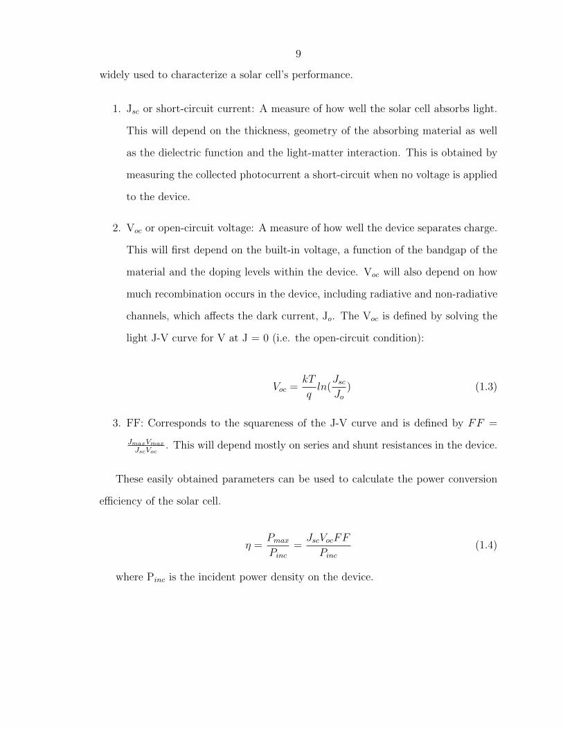
9
widely used to characterize a solar cell’s performance.
1. Jsc or short-circuit current: A measure of how well the solar cell absorbs light.
This will depend on the thickness, geometry of the absorbing material as well
as the dielectric function and the light-matter interaction. This is obtained by
measuring the collected photocurrent a short-circuit when no voltage is applied
to the device.
2. Voc or open-circuit voltage: A measure of how well the device separates charge.
This will first depend on the built-in voltage, a function of the bandgap of the
material and the doping levels within the device. Voc will also depend on how
much recombination occurs in the device, including radiative and non-radiative
channels, which affects the dark current, Jo. The Voc is defined by solving the
light J-V curve for V at J = 0 (i.e. the open-circuit condition):
Voc =kT
qln(
JscJo
) (1.3)
3. FF: Corresponds to the squareness of the J-V curve and is defined by FF =
JmaxVmaxJscVoc
. This will depend mostly on series and shunt resistances in the device.
These easily obtained parameters can be used to calculate the power conversion
efficiency of the solar cell.
η =PmaxPinc
=JscVocFF
Pinc(1.4)
where Pinc is the incident power density on the device.
10
1.3 Current State Of The Art Solar Cells
Using the method of Shockley and Quiesser, the maximum theoretical efficiency of a
single junction solar cell of any given material can be calculated. All that is needed is
an incident spectrum and the bandgap energy of the semiconductor. Two of the most
important solar cell materials are Si and GaAs. The maximum efficiency of a single
junction Si solar cell under the AM1.5G solar spectrum is about 30%. Currently,
the highest achieved efficiency for a Si solar cell is 25% [14]. This efficiency for Si
is currently limited by non-radiative recombination processes intrinsic to Si, such as
Auger recombination. The thickness of typical record Si devices is usually above 50
microns. A Si record cell could benefit from advanced light trapping by significantly
reducing the amount of active material needed, potentially down to below 5 microns,
or more than an order of magnitude.
The theoretical maximum efficiency for a GaAs solar cell is about 33%. The
current maximum achieved efficiency is 28.8% [14], by Alta Devices [15] using the
epitaxial liftoff process of delaminating a thin film of GaAs from its parent substrate
and adding a back reflector. All three of the important solar cell parameters are
just slightly below their theoretical maximum values. A GaAs cell could benefit from
advanced light trapping by reducing the amount of material needed to absorb the
spectrum, potentially increasing the voltage by reducing the volume-dependent dark
current.
1.4 Why Thin Solar Cells?
Despite the best Si solar cells being many tens of microns thick, the ultimate solar
cell is one that is as thin as possible. There are many advantages for thinning the
active layer, with the obvious disadvantage that it decreases light absorption. If the
exponential reduction in absorption while thinning the cell can be prevented, a solar
11
cell could gain the following benefits:
• Reduced Cost
The most obvious advantage of a thin solar cell is that is reduces the amount of
raw material needed to make the device. As of 2012, about 60% of a Si module
cost is due to the Si alone [16]. Reducing the thickness of a Si device by an
order or magnitude or more could significantly decrease this cost.
If the solar cell is made from an epitaxial material like a III-V, reducing the
active layer thickness will decrease both the amount of precursor gas needed
for growth as well as reactor run time for each device. Though direct bandgap
materials like GaAs are already relatively thin (∼2-5 microns) compared to Si,
their thickness could still in theory be reduced to below a micron, as will be
shown in the next section.
• Flexibility
While a crystalline wafer of a semiconductor such as Si or GaAs is extremely
brittle and can crack or shatter if handled improperly, a thin film of these
materials can be extremely flexible. This opens up many new applications
for solar power that otherwise would not be feasible with wafer-based devices.
For example, a flexible module could be rolled out and used when needed as
portable charging station, and rolled back up and stored conveniently when
not needed. A flexible device could be incorporated into clothing or baggage,
wrapped around curved surfaces, or even integrated into the outside of an au-
tomobile or aircraft.
• Improved Voc and Efficiency
Perhaps the most intriguing motivation for making a solar cell as thin as possible
is an increased operating voltage and possibility of an overall increased efficiency

12
compared to a thicker device. This is because the dark current density, Jo, is a
function of the total recombination within the device. The more bulk material
there is in the device, the more bulk recombination and the higher the dark
current. This lowers the Voc as shown in Equation 1.3. Plotted in Figure
1.2a is a calculation of the Voc as a function of thickness for a GaAs solar cell
with various amounts of bulk non-radiative recombination current. Also shown
is how the Jsc decreases with thickness when there is only a single photonic
pass. Clearly, in order to take advantage of the increased Voc for thinner cells,
significant light trapping is needed to maintain the Jsc of thicker cells. Shown in
Figure 1.2b is the calculated efficiency of a GaAs cell with various amounts of
light trapping. It can be seen that with increased light trapping, the maximum
possible efficiency increases and occurs at thinner and thinner cells. Since both
Voc and Jsc need to be maximized to increase efficiency, the ideal solar cell is
one that is as thin as possible yet still absorbs the available light from the sun.
0"
0.05"
0.1"
0.15"
0.2"
0.25"
0.3"
0.35"
10" 100" 1000" 10000"Cell$Thickness$(nm)$
Jsc"Max"(Absorp4vity"="1)"
Ergodic"Limit"
5"Passes"
2"Passes"
1"Pass"
Effic
ienc
y Voc (V)
a) b)
Cell Thickness (μm) Cell Thickness (μm)
J sc (
mA/
cm2 )
Figure 1.2: a) Effect of thinning a solar cell on Jsc and Voc with no light trapping.NR is the amount of non-radiative recombination. b) Efficiency as a function of cellthickness with various amounts of light trapping. The more light trapping, the higherthe maximum possible efficiency.

13
Chapter 2
Light Trapping In Thin Film SolarCells
2.1 Single Pass Absorption
Photons with energy above a semiconductor’s bandgap can be absorbed if given
enough time to interact with the material. How quickly light is absorbed depends on
the complex dielectric function of the material (i.e. refractive index and absorption co-
efficient), and the nature of the light-matter interaction. For light propagating freely
as a plane wave in a homogeneous material, the amount absorbed, or intensity I, is
exponentially dependent on how far it travels, given by the well known Beer-Lambert
law:
I(z) = Ioeαz (2.1)
A commonly used metric for electromagnetic absorption is the absorption depth,
1α
defined as or the depth at which the intensity of a wave decays to 1e
(about 35%)
of its initial value. Plotted in Figure 2.1 is the absorption depth for some common
semiconductors.
A few things are clear from this plot. First, some materials absorb light much
more strongly than others. For example, a direct bandgap material like GaAs has a

14
Figure 2.1: Absorption depth for common photovoltaic materials used in this thesis.
1
10
100
1000
10000
100000
1000000
200 300 400 500 600 700 800 900 1000 1100
Abso
rptio
n D
epth
(nm
)
Wavelength (nm)
GaAs Si a-Si
Figure 2.1: Absorption depth for common photovoltaic materials used in this thesis.
much shorter absorption depth across the entire spectrum compared to an indirect
semiconductor like Si. This will dictate typical thicknesses for each type of solar cell,
with GaAs solar cell thicknesses being a few microns and Si thicknesses being many
tens or even hundreds of microns. Second, for nearly all materials, the absorption
depth is a strong increasing function of wavelength. This has strong implications for
light trapping, as the wavelengths that need the most consideration will be the longer
ones, and the bandwidth of interest will depend on the thickness of the material.

15
2.2 Modes Of A Slab
In order to design structures for light trapping, an understanding of the optical modes
of a semiconductor slab is critical. Consider a dielectric slab of material with a
refractive index, n2, surrounded by an upper dielectric material with index, n1, and
a lower dielectric with index n3. Following Yariv [17], we find that different types
of electromagnetic modes exist in the slab for a single frequency. Modes that have
oscillating field components both inside and outside the slab are known as radiation
modes. Modes which are oscillating inside the slab but decay exponentially outside
the slab are known as bound or trapped modes. Each of these will be described in
more detail below.
The nature of the modes of a slab depends on the relative surrounding refractive
indices and a very important quantity known as the propagation constant, β, or in-
plane wavevector, k||. It is useful to plot the relationship of wavevector and frequency
in a dispersion diagram, as is shown in Fig. 2.2a,d. From this single diagram, we can
describe and understand the modes that exist in most photonic structures.
We start with the definition of wavevector for a plane wave propagating in a
homogeneous medium:
ω =ck
n(2.2)
where c is the speed of light and n is the refractive index of the material the
photon is propagating in. If we define the in-plane wavevector k|| as the component
of the wavevector in the plane of the slab, we can start to describe the photon with
the dispersion diagram. For a photon propagating inside the incident material with
index, n1, it will have a k|| of 0 when it is normal to the plane of the slab. As the
incident angle in increased off-normal, it will gain a parallel component dependent on
the angle and its frequency:
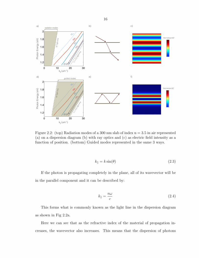
16
0 10 20 30
1.2
1.4
1.6
1.8
2300nm n=3.5 in Air
k|| (um−1)
Phot
on E
nerg
y (e
V)
TEoTMoTE1TM1Air LigSlab LTE2
Figure' 2.2:" (top)" Radiation" modes" of" a" slab" represented" (a)" on" a" dispersion"diagram" (b)" as" electric" 6ield" intensity" as" a" function" of" position" and" ©"schemcatically" in" terms" of" propagation" angles." (bottom)" radiation" modes"represented"in"the"same"3"ways."
0 10 20 30
1.2
1.4
1.6
1.8
2300nm n=3.5 in Air
k|| (um−1)
Phot
on E
nerg
y (e
V)
TEoTMoTE1TM1Air LigSlab LTE2
Phot
on E
nerg
y (e
V)
Phot
on E
nerg
y (e
V)
k|| (um-1)
k|| (um-1)
air l
ight
line
ai
r lig
ht li
ne
radiation modes
guided modes
Normalized |E|2
a) b) c)
d) e) f)
Normalized |E|2
Figure 2.2: (top) Radiation modes of a 300 nm slab of index n = 3.5 in air represented(a) on a dispersion diagram (b) with ray optics and (c) as electric field intensity as afunction of position. (bottom) Guided modes represented in the same 3 ways.
k|| = k sin(θ) (2.3)
If the photon is propagating completely in the plane, all of its wavevector will be
in the parallel component and it can be described by:
k|| =nω
c(2.4)
This forms what is commonly known as the light line in the dispersion diagram
as shown in Fig 2.2a.
Here we can see that as the refractive index of the material of propagation in-
creases, the wavevector also increases. This means that the dispersion of photons

17
propagating in higher indices will appear towards the right on the dispersion dia-
gram.
A photon incident on a planar slab at any of these angles will refract at an angle
according to Snell’s law, propagate through the slab at that angle, and exit the slab
again at an angle according to Snell’s law (at each interface, of course, portions will
not only be refracted but also reflected as dictated by the Fresnel equations). This is
commonly known as a single pass through the material and would result in minimal
absorption if the material were a solar absorber. Adding a back reflector will only add
a second pass, with the photon exiting from the top instead of the bottom if it is not
absorbed. The set of modes and corresponding in-plane wavevectors associated with
this are known as radiation modes and are shown in three different descriptions in
Fig 2.2a-c. It is important to note that for a planar interface, these radiation modes
are the only modes that can be accesed by photons incident from free space, which
only results in 1-2 passes depending on if there is a back-reflector or not.
Photons that gain extra in-plane momentum (k||) can access another set of modes
that exist in the slab, called bound modes. These modes can be understood from
a ray optics perspective as light trapped by total internal reflection. In the wave
optics picture, these modes have oscillating fields within the slab and exponentionally
decaying fields outside the slab. These modes will have in-plane wavevectors between
the light line of the incident medium and the light line of the bulk medium of the
slab, given by ω = ckn2
. They form discreet bands in the dispersion diagram and may
have multiple solutions at a single frequency corresponding to different mode orders.
These modes are calculated and shown in Fig. 2.2d-f in 3 different representations
for a 300 nm slab with refractive index 3.5 surrounded by vacuum.
A photon or wave in a trapped mode will stay trapped forever unless 1) something
changes its momentum (k||) by scattering or diffracting it out of the waveguide or into
a different mode or 2) it is absorbed (if the material is absorbing at that wavelength).

18
Similarly, as stated before, a photon starting out in the lower index incident medium
cannot enter one of these trapped modes unless something changes its momentum.
Clearly, a photon trapped in a bound mode (having many effective passes) has a
much greater chance of getting absorbed than a photon in a radiation mode (only 1-
2 passes). Getting photons from free space with low in-plane momentum into trapped
modes where they can be most efficiently absorbed is the central goal of solar cell
light trapping.
2.3 Accessing Trapped Modes
In order for a photon incident from free space to access the guided modes of a slab, its
in-plane momentum must be changed so that it matches that of the trapped modes.
A photon can elastically scatter off of a particle that has dielectric contrast with
its surroundings if the particle’s size is comparable to the wavelength. This will
alter the momentum of the photon and may allow it to couple to nearby optical
modes with various momenta. In the wave picture, this occurs because the photon is
localized during the scattering event, introducing new, larger k-vectors (modes in k-
space are inversely proportional to modes in real space) in the vicinity of the scattering
particle [18]. If the particle is close enough to an optical mode (e.g. a guided mode of
a slab), and the fields overlap, the energy of the incident wave can be transferred to
the optical mode. In the quantum picture, scattering events are described by Fermi’s
golden rule, which states that a scattering event will send the scattered particle (i.e.
a photon) into a new state depending on the nearby density of states. As we will see
in the next section, a dielectric slab with a higher index than the incident medium has
a higher density of optical states than its surroundings, and will preferentially accept
photons scattered at the interface between the two media. A single isolated scatterer
or a set of random, uncoupled scatterers will ideally redistribute the incident light in

19
many different directions, or angles from its incident angle.
Figure' 2.2:" (top)" Radiation" modes" of" a" slab" represented" (a)" on" a" dispersion"diagram" (b)" as" electric" 6ield" intensity" as" a" function" of" position" and" ©"schemcatically" in" terms" of" propagation" angles." (bottom)" radiation" modes"represented"in"the"same"3"ways."
0 10 20 30
1.2
1.4
1.6
1.8
2300nm n=3.5 in Air
k|| (um−1)
Phot
on E
nerg
y (e
V)
TEoTMoTE1TM1Air LigSlab LTE2
Phot
on E
nerg
y (e
V)
k|| (um-1)
b) Δk = 2πΛ
Λ
a)
0 10 20 30
1.2
1.4
1.6
1.8
2300nm n=3.5 in Air
k|| (um−1)
Phot
on E
nerg
y (e
V)
TEoTMoTE1TM1Air LigSlab LTE2
Phot
on E
nerg
y (e
V)
k|| (um-1)
d) Δk = 2π
Λ
Λ
c)
k|| = 0
kz
k
k|| = k sin(θ)
kz
k
θ
Figure 2.3: Coupling into a slab with a diffraction grating. The interscting lines in(b) and (d) occur at wavelengths where light can be coupled into guided modes at agiven angle. (top) Normal incidence. (bottom) Off-normal incidence.
Another way to access the guided modes of a slab is through diffraction. Diffrac-
tion can be viewed as a series of scattering events with the scatterers arranged in
an ordered, periodic pattern. In the wave picture, certain angles of propagation are
allowed due to constructive interference between the scattered waves, and other an-
gles disallowed due to destructive interference. An ordered array of scatterers with
period Λ, will add and subtract in-plane momentum from an incident plane wave
with values of 2πnΛ
, where n is an integer. These new values of in-plane momentum
20
can also correspond to new angles of propagation given by the diffraction equation:
mλ = Λsin(θm) (2.5)
where λ is the wavelength of light and m is an integer. This is schematically shown
in Fig. 2.3a using the dispersion diagram of Fig. 2.2. Light can be coupled into the
slab at the locations where the diffraction lines intersect the bands corresponding to
the trapped modes of the slab. If the incident angle is changed, the starting value of
k|| will change, but the values of added momentum will not. This will only change
the resonant wavelengths which couple into the slab as shown in Figure 2.3b. It is
important to note that at a given angle, there is only a subset of available modes
that can be accessed with a diffraction grating (i.e. the intersecting lines in Fig. 2.3),
depending on the period of the grating and the incident angle. Alternately, scattering
from single point sources or random surfaces as previously described can potentially
couple light into all of the available modes of the slab. If the scattering surface is
ideal, it will also do this at all angles. For this reason, random scattering surfaces are
typically more useful for broadband, varied angle incoupling for applications such as
solar cells.
2.4 The Ray Optic Light Trapping Limit
In 1982, Yablonovitch [19] published a theory describing a fundamental limit to how
much light trapping could be achieved in a thin slab of semiconductor with ideal
scattering surfaces. This limit is known as the ray optic light trapping limit, also
often called the ergodic limit.
Yablonovitch arrives at this limit by considering a homogeneous slab of material
with a refractive index, n, and immersing it in a vacuum (with refractive index 1
by definition) that contains blackbody radiation at a temperature, T. When the

21
radiation inside the slab reaches equilibrium with its surroundings, we can compare
energy densities inside and outside the slab:
Uin(r, ω) =n3ω2
π2c3· 1
ehωkT − 1
· hω (2.6)
Uout(r, ω) =ω2
π2c3· 1
ehωkT − 1
· hω (2.7)
They clearly only differ by a factor of n3.
Absorption is directly related to optical intensity, so by converting the energy
density to an intensity by multiplying by the group velocity vg = dωdk
and using the
well known relation ω = ckn
, the intensities become:
Iin(r, ω) =n2
π2c2· hω3
ehωkT − 1
(2.8)
Iout(r, ω) =1
π2c2· hω3
ehωkT − 1
(2.9)
Which differ by only n2. If a simple back reflector is added to add a second pass
for any light that escapes the rear of the slab, this intensity enhancement increases to
2n2. After averaging over all angles using a ray optics approach, Yablonovitch comes
to an overall absorption, or path length, enchancement of 4n2.
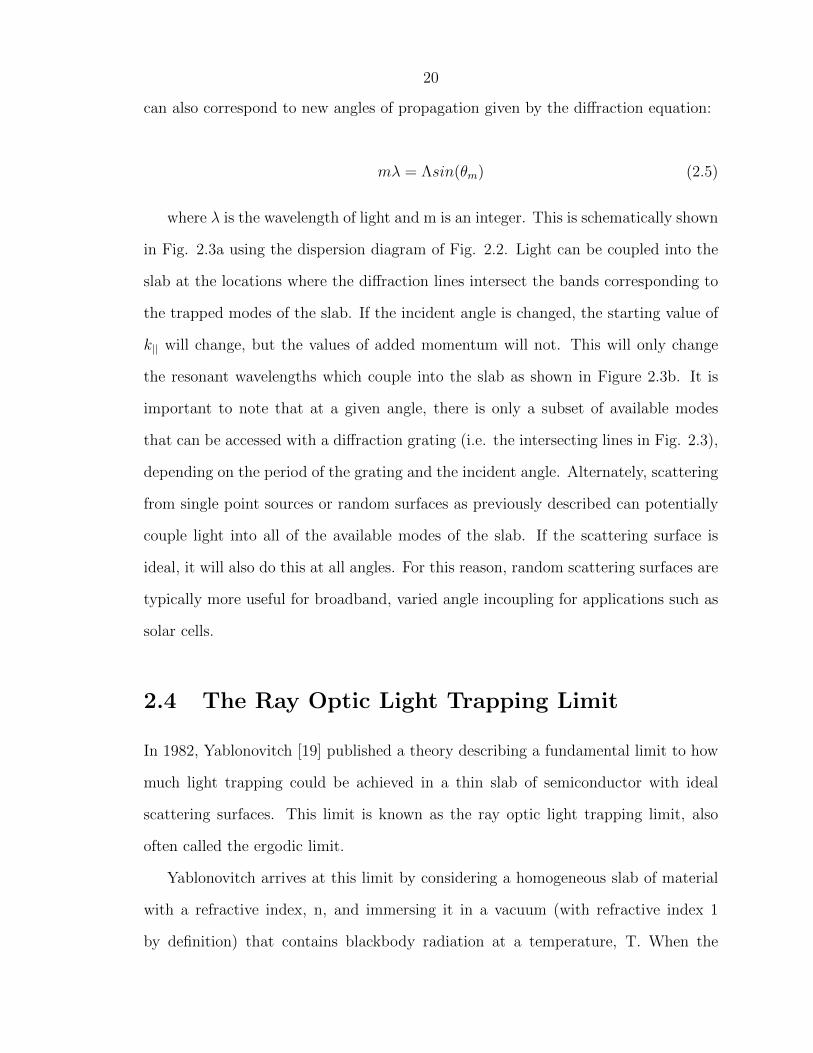
Figure 2.4: (a) modes of a planar slab accessed (grey regions) at all incident angles, (b) modes of a Lambertian textured slab accessed at all incident angles.
Ω
2π 2π
2π (4π w/BR)
a) b)
Figure 2.4: (a) Modes of a planar slab accessed at all incident angles, (b) Modes of aLambertian textured slab accessed at all incident angles.
22
An intuitive way to understand where the 4n2 path length enhancement comes
from is by considering the escape cone for light inside the slab. As mentioned pre-
viously, a subset of modes known as radiation modes exist inside the slab and can
be accessed from free space. If the angle of incident light were swept through all 2π
steradians outside the slab as shown in Fig. 2.4, the refracted rays inside the slab
would sweep out a cone known as the escape cone. The solid angle, Ω, of this cone
is less than the 2π steradians outside because of Snell’s law of refraction and the fact
that the index of the slab is higher than free space. Any angles outside of this cone
correspond to trapped modes of the slab and cannot be accessed from free space with-
out a momentum changing event. Now, consider a slab with perfectly Lambertian
textured surfaces. These surfaces will scatter the light ideally into all 4π steradians
that exist inside the slab. This ratio of internal angles, or modes accessed, gives the
4n2 light trapping limit.
4π
Ω≈ 4n2 (2.10)
by series expansion and trigonometric identity where Ω = 2π(1 − cos θ) and θ =
sin−1( 1n). In this sense, reaching the light trapping limit can be understood as when
incident light is able to access all of the modes inside the slab (both radiative and
bound).

23
Chapter 3
Light Trapping Beyond The RayOptic Limit
To utilize many of the benefits of ultrathin solar cells, the active layers for most ma-
terials have to be reduced to thicknesses where traditional light trapping is no longer
effective. At some point, even light trapping that reaches the ray optic, ergodic limit
is not enough to generate reasonable short circuit currents, particularly in the wave-
length range near the semiconductor bandgap. For any given thickness, there is a
range of wavelengths that is near fully absorbed upon 4n2 optical passes and another
range that is not fully absorbed due to the exponential nature of the absorption pro-
cess and the fact that the absorption coefficient approaches zero at the semiconductor
band edge (Fig. 2.1). Therefore we can divide our conceptual approach to the light
trapping limit between the spectral region where enhanced absorption is needed and
where it is not. The transition region between these two regimes depends on the
material properties, thickness, structure, etc.
There is previous evidence that solar cells with non-slablike geometries that op-
erate in the wave optic rather than ray optic limit may exceed this limit [20–24],
and recent theoretical work has successfully explained the phenomena in selected
cases [25, 26]. The theory of Yu et al. establishes a relationship between the modes
supported in a slablike solar cell and the maximum absorption attainable but is not
easily extensible to the broad portfolio of light trapping schemes currently being ex-

24
Figure 3.1: Traditional limits to photogenerated current. (a) Current density resulting from AM1.5 solar spectrum absorption for various thicknesses of a bulk slab of Si (inset) assuming either exponential absorption from a single pass or 4n2 passes at the ergodic light trapping limit. (b) Spectrally resolved absorbed current for a 100 nm slab of Si with light trapping at the ergodic limit. There is a significant region near the band edge where increased light trapping is needed beyond the ergodic limit. (c) A thin slab of semiconductor where the LDOS is affected by a lower index surrounding environment and (d) a higher index surrounding environment..
Figure 3.1: Traditional limits to photogenerated current. (a) Current density resultingfrom AM1.5 solar spectrum absorption for various thicknesses of a bulk slab of Si(inset) assuming either exponential absorption from a single pass or 4n2 passes at theergodic light trapping limit. (b) Spectrally resolved absorbed current for a 100 nmslab of Si with light trapping at the ergodic limit. There is a significant region nearthe band edge where increased light trapping is needed beyond the ergodic limit. (c)A thin slab of semiconductor where the LDOS is affected by a lower index surroundingenvironment and (d) a higher index surrounding environment.
plored in the literature [11,21,27].
We find that a common defining feature of light trapping structures that can ex-
ceed the ray optic limit is that the electromagnetic local density of optical states
(LDOS) integrated over the active absorber region must exceed that of the corre-
sponding homogeneous, bulk semiconductor. That the density of optical states plays
an important role in defining the light trapping limit has been alluded to in previous
work [25, 28, 29], and we use it here as a defining approach for understanding light
trapping. We develop a unified framework for thin film absorption of solar radiation
and show that an enhanced integrated LDOS is the fundamental criterion that de-

25
termines whether light trapping structures can exceed the ray optic light trapping
limit, leading to a strategy for design of solar absorber layers with wavelength-scale
characteristic dimensions that exhibit optimal light trapping.
3.1 Condition for Exceeding The Ray Optic Limit
As in the original ray optics formulation [19], the electromagnetic energy density
serves as a starting point for examining the partitioning of energy between the solar
cell and the surrounding environment. For any given geometry, the electromagnetic
energy density is a function of position. One way to express the electromagnetic
energy density is in terms of the local density of optical states (LDOS), ρ(r, ω), the
modal occupation number 〈ν〉, and the energy of each mode, hω:
U(r, ω) = ρ(r, ω) · 〈ν〉 · hω (3.1)
The modal occupation number is summed over all modes of the structure. In a
homogeneous environment with refractive index, n, and with purely thermal Bose-
Einstein occupation, the electromagnetic energy density takes the familiar form:
U(r, ω) =n3ω2
π2c3· 1
ehωkT − 1
· hω (3.2)
By examining the ratio of energy densities inside and outside the solar cell at
thermal equilibrium, we can determine the maximum light intensity enhancement
and thus the maximum light trapping that is possible [19]. We do this by taking the
ratio of electromagnetic energy densities in two distinct cases of interest. This gives
an important ratio, that includes the LDOS ratio and the modal occupation number
ratio:

26
U(r, ω)case1U(r, ω)case2
=ρ(r, ω)case1ρ(r, ω)case2
· 〈ν〉case1〈ν〉case2
(3.3)
This same ratio can be obtained by starting with an expression for the local
absorption rate:
A(r, ω) =1
2ω · ε′′(r, ω) · E(r, ω)2 (3.4)
The absorption can be related to the energy density by rewriting the energy density
in terms of the ambient dielectric function and the electric field intensity. In limit of
a lossless, dispersionless medium:
U(r, ω) =1
2ε(r, ω) · E(r, ω)2 +
B(r, ω)2
2µ(r, ω)= ε(r, ω) · E(r, ω)2 (3.5)
Equating this with equation 3.1 and rearranging we have for the electric field
intensity:
E(r, ω)2 =1
ε(r, ω)· ρ(r, ω) · 〈ν〉 · hω (3.6)
We can insert this into our expression for local absorption rate to determine how
the LDOS and modal occupation number affect absorption:
A(r, ω) =1
2ε(r, ω)· ε′′ · ρ(r, ω) · 〈ν〉 · hω2 (3.7)
Because equations 1 and 4 assume lossless materials, we can only introduce a
small amount of absorption before these concepts become ill-defined. It is neverthe-
less common to use expressions like this in the limit of low absorption to describe
light trapping phenomena, as has been done both in the original derivation [19] and
subsequent treatments [25,26]. We will find next, however, that Eq. 3.7 is not neces-
sary but rather has been used to verify the importance of energy density ratios. As

27
with the expressions for energy density, we can now take the ratio of local absorption
rate for 2 distinct cases of interest and again obtain Eq. 3.3.
We can use this ratio to examine numerous cases of interest. In the limit of large
thicknesses, we will recover the ray optic light trapping limit for homogeneous mate-
rials in Section 3.2. First, we compare a homogeneous absorber with an arbitrarily
designed absorber that may be capable of exceeding the ray optic light trapping limit:
ρ(r, ω)case1ρ(r, ω)case2
· 〈ν〉case1〈ν〉case2
=ρ(r, ω)cellρ(r, ω)bulk
· 〈ν〉cell〈ν〉bulk
(3.8)
where we have assumed integration over all modes of the structure. When an
incoupling mechanism fully populates the modes of each structure, the light trapping
enhancement is simply the LDOS ratio between the cell structure and a homogeneous
bulk structure which achieves the ergodic limit. This implies that if the LDOS of the
cell structure is larger than that of a homogeneous medium with the same refractive
index, the ergodic light trapping limit can be exceeded. Inputting the expression for
LDOS of a homogeneous medium with refractive index n, we reach the condition for
exceeding the ergodic limit:
π2c3
n3ω2ρ(r, ω)cell > 1 (3.9)
assuming that all modes of the structure are fully occupied via an appropriately
designed light incoupler, which is often taken to be a Lambertian scattering surface.
We now briefly discuss the importance of fully populating the modes of the arbi-
trarily designed solar cell structure. As the ratio of equation 3.8 indicates, a structure
with an elevated LDOS is necessary but not sufficient to exceed the light trapping
limit, which also depends on the modal occupation numbers. There are numerous
examples of solar cell structures that very likely have an elevated LDOS; however,
whether or not they have exceeded the traditional light trapping limit has remained
28
uncertain [20, 23]. Structures that use diffractive elements such as gratings and pho-
tonic crystals often couple into only a small subset of the available modes, dictated
by momentum conservation. This severely limits the number of modes that are oc-
cupied, much like the above-mentioned case of a planar interface. If these structures
were integrated with a scattering layer, the full modal spectrum of the device could
in principle be excited, and much more light could be absorbed within the solar
cell. This would also resolve the relevant problem of limited angular and polarization
response associated with many designs. We also note that full modal occupation
is not necessary to surpass the ergodic limit, as will be shown below using FDTD
calculations.
3.2 Recovering The Ray Optic Limit
Considering first a bulk, homogeneous slab of semiconductor with a planar interface,
we find that light incident from all 2 steradians gets coupled into a small subset of the
modes within the slab given by the escape cone defined by Snell’s law. We call these
radiation modes. We assume that all incident light is transmitted to the solar cell, thus
each of these radiation modes is fully occupied with the maximum occupation number
defined through the modified radiance theorem [30,31]. Each incident mode contains
an occupation number, νinc, and is mapped into a single radiation mode within the
semiconductor defined by Snell’s Law with maximum occupation number νmax =
νinc [30, 31]. No more light can be coupled into these radiation modes within the
slab as they are fully occupied to the maximum extent dictated by thermodynamics.
There are of course 4π - Ω modes inside the semiconductor left unoccupied in this
case, and we call these trapped or evanescent modes [30]. These trapped modes are
inaccessible from free space without a momentum changing event such as scattering
or diffraction. We count the number of excitations within the slab by multiplying the

29
number of modes accessed by their occupation number.
We now look at the same slab of semiconductor with a lambertian scattering
surface. We assume that this surface does not alter the density of states within the
slab as is often assumed [19,30]. This means that when we take the ratio of equation
3.8, the LDOS terms will cancel, and we will be left considering only the difference in
modal occupation numbers. For an incident mode with occupation number νinc, the
scattering event splits the energy in this mode between all equal modes within the
semiconductor. Thus, each of the internal modes, both radiation and trapped, now
have a fraction of this energy, let us say νinc4π
. This means that each of the internal
modes can be fed more energy as their occupation numbers are not at their maximum
value. We can continue to couple light into the semiconductor until each of these 4π
internal modes has an occupation number νmax = νinc. We again count the number
of excitations by multiplying the number of modes by their occupation numbers. We
can now take the ratio in equation 3.8 for each of these two cases,
ρ(r, ω)lambertianρ(r, ω)planar
· 〈ν〉lambertian〈ν〉planar
=〈ν〉lambertian〈ν〉planar
=4π〈ν〉incθc〈ν〉inc
=4π
θc≈ 4n2 (3.10)
where we have assumed integration over all modes of the structure. This gives the
traditional, or ergodic, light trapping limit.
3.3 Nanophotonic Solar Cell Designs For Exceed-
ing The Ray Optic Light Trapping Limit
We now outline a portfolio of wavelength-scale solar absorber layer designs that ex-
hibit an LDOS modified relative to that of a homogeneous slab of the same material.
We begin by examining ultrathin, planar solar cells for which we calculate the LDOS

30
as a function of position within the semiconductor using the Greens dyadic for a lay-
ered planar system [10, 18, 32] and then integrate over position to get the spatially
averaged LDOS. For the case of a finite thickness planar absorber, in Fig 3.1c-d, the
LDOS modification can be viewed heuristically in terms a slab of thickness t with a
homogeneous LDOS (LDOSo) which is modified from its surface to some depth tm by
the LDOS of the neighboring material. In Fig. 3.2 we plot this averaged LDOS en-
hancement for various absorber structures as a function of thickness and wavelength.
When t >> 2tm, the absorber LDOS modification by the surrounding materials is
negligible, but when t ≈ 2tm the change in the absorber layer LDOS due to the in-
fluence of surrounding materials becomes significant. First, in Fig. 3.2a we note that
the integrated LDOS for a thin semiconductor slab surrounded by free space or lower
index materials is always less that that of its corresponding bulk material as the slab
thickness is reduced, implying that the light trapping limit in this structure is actually
lower than that of the same material in bulk form. This has been pointed out before
using a different methodology [30]. However, when the surrounding material includes
a metal back reflector as shown in Fig. 3.2b, the integrated LDOS can exceed that of
its corresponding bulk material in finite thickness layers, particularly for thicknesses
below 200-300 nm. Further, the metal-insulator-metal (MIM) structure shown in Fig.
3.2c exhibits an integrated LDOS enhancement relative to its corresponding bulk ab-
sorber material that is very significant for all thicknesses below 500nm, exceeding 50
for all relevant wavelengths with ultrathin layers below 20 nm.
For a two-dimensional planar structure, the modal density of states can be ob-
tained from the optical dispersion relations. In this case, the density of guided modes
per unit area per unit frequency for the mth mode can be written as [30]:
ρm =km2π
(dω
dkm
)−1
(3.11)
where km is the propagation constant. In order to increase the density of modes

31
Figure 3.2:
Ener
gy (e
V)
k(nm-1)
(μ
m)
Thickness (μm)
1
0.4
400
1.1
1"0"0.4
1.2
1.2
3.0
1000
1.1
13
1.7
absorber absorber metal metal
metal
absorber low index high index
high index
Bulk Si
thin Si slab (large & slow vg) Bulk Si
SPP mode (slow vg)
Bulk n=2
Slot waveguide
Bulk Si
(large & slow vg)
Thickness (μm) 1"0"
Thickness (μm) 1"0"
Thickness (μm) 1"0"
228
1
Thickness (μm) 0.1 0.02
550
1
x position (nm) 100 0
6.8
0.05
A
B C
DGaAs
A B C D
"0""""""""""""""""""""""""""""2""LDOS"Enhancement"
(a) (b) (c) (d) (e) (f)
1.0
1.5
2.0
2.5
3.0
0.0
0.5
1.0
1.5
2.0
Wavelengthnm
Averaged LDOS Enhancement
GaAsPhCSolarCellLDOSEnhancement
k(nm-1) k(nm-1) k(nm-1)
Figure 3.2: Potential solar cell architectures. (a) Planar slab of Si in air in whichthe LDOS is always below the bulk value. Structures with the potential to beat theergodic limit: (b) planar slab of Si on an Ag back reflector, (c) Ag/Si/Ag planarstructure, (d) high/low/high index structure with refractive indices 3/1.5/3, (e) aphotonic crystal with index 3.7, and (f) a split dipole antenna made of Ag with a Sigap. The second row shows the LDOS enhancement (on a log color scale) over thebulk material for each structure for various cell thicknesses and wavelengths. Valuesof LDOS enhancement > 1 correspond to beating the traditional absorption limit.For (a - d), the bottom row shows examples of the 2D modal dispersion curves for eachstructure. The bottom of column e shows that the integrated LDOS enhancement > 1for most wavelengths, and the bottom of column f shows the wavelength dependentLDOS enhancement > 1 for radial positions between the split dipole.
above the homogeneous value, either km > k0 or vm = dωdkm
< vo , where k0 and v0 are
the homogeneous values of the propagation constant and group velocity, respectively.
Figure 3.2 also shows for each planar structure examples of the modal dispersion
relations, showing regions where the density of states is increased due to either slow
(low group velocity) modes or large in-plane propagation constants. Note that these
dispersion plots do not fully depict the total LDOS, due to the existence of multiple
modes; however, many of the key features can be obtained from the dispersion rela-
tions. A full 2D waveguide formulation requires a slightly different analysis, which

32
will be the subject of section 3.4. For the metallodielectric structures, the plasmonic
modes that contribute to the LDOS enhancement exhibit parasitic Ohmic metallic
losses, and so exceeding the light trapping limit in any structure incorporating metals,
requires the useful absorption within the solar cell semiconductor absorber layer to
dominate over parasitic metallic losses. This represents a challenge for successful im-
plementation of certain cell designs incorporating metals, but we demonstrate below
that it is possible to exceed the light trapping limit in metallodielectric structures
with proper design.
A analogous planar structure without metallic losses is a dielectric slot waveguide
[33] in which a low index absorber material is sandwiched between two nonabsorbing
cladding layers of higher index, shown in Fig. 3.2d for a core of dielectric constant 1.5
and a cladding of dielectric constant 3. The LDOS within the low index slot will be
increased due to the presence of the high index cladding layers, which have an LDOS
significantly higher than that for a bulk slab of the low index material. Over the entire
range of the solar spectrum there is a significant integrated LDOS enhancement in
the dielectric slot (Fig. 3.2d). This effect can also be observed for common inorganic
semiconductor materials such as GaP and CdSe. We perform a similar calculation
to Fig. 3.2d using the dielectric functions of these realistic, all inorganic materials.
For the cladding layer we use the weakly absorbing indirect semiconductor GaP and
for the core we use CdSe. These materials fit the criterion at all wavelengths of
interest that the refractive index of the core is lower than that of the cladding. In
Fig. 3.3 we plot the spatially averaged LDOS enhancement within the CdSe slot for
various slot thicknesses. It can be seen that over all wavelengths of interest there is
an increased LDOS due to the slot waveguide effect, becoming more pronounced as
the slot thickness is reduced.
Dielectric slot waveguides have considerable potential as structures to achieve
absorption enhancement in polymer and low index solar cells as there is no metallic

33
1100 1000 900 800 700 600 500 400
Figure 3.3: (a) Schematic of slot waveguide structure using realistic materials GaP and CdSe. (b) Averaged LDOS enhancement within the CdSe slot as a function of slot thickness with a constant total device thickness of 1um.
1 um total
3.8
1.08
Log
LDOS Enhancement
vary t
GaP
CdSe
GaP
Wav
elen
gth
(nm
)
0 20 40 60 80 100 Slot Thickness, t (nm)
Figure 3.3: (a) Schematic of slot waveguide structure using realistic materials GaPand CdSe. (b) Averaged LDOS enhancement within the CdSe slot as a function ofslot thickness with a constant total device thickness of 1um.
loss mechanism. This phenomenon for similar structures has also been recognized in
two recent works using different methodologies [25,26].
Next we examine other structures with potential to exceed the light trapping
limit. Photonic crystals [5,34] are interesting candidates as they are known to possess
elevated LDOS around flat bands in their dispersive bandstructures. There are a
least two ways that photonic crystals can be taken advantage of for solar cells. A
photonic crystal could be carved out of a bulk, planar solar cell, or an unstructured,
planar solar cell could be integrated with a photonic crystal. The former is certainly
intriguing as large LDOS enhancements would be expected but has issues regarding
increased surface recombination associated with nanostructuring the active region.
Still, utilizing a liquid junction [21] or appropriate passivation of a solid state surface
[35] could solve this problem. Here we consider integrating a non-absorbing planar
photonic crystal with an unstructured, planar solar cell. This could be easily realized
by making the photonic crystal out of an anti-reflection coating material such as
SiNx, ZnS or TiO2, or by patterning a window layer such as AlGaAs or InGaP on
a III-V solar cell such as GaAs. Here, we take a material of index 3.7, common

34
for III-V materials like GaAs, InGaP, and AlGaAs, and create a hexagonal lattice
of air holes in it with a radius of 205 nm and lattice constant of 470 nm. These
parameters are designed so that there is a slow mode with high density of states at
the GaAs bandedge at 870 nm. We put this photonic crystal on a thin 10 nm planar
layer of the same material and calculate the LDOS as a function of position in the
middle of the 10 nm plane. In Fig 3.4a it can be seen that there are significant LDOS
enhancements at various positions throughout the structure. In Fig 3.4b we also show
the spatial LDOS profiles for select wavelengths. It can be seen that at the bandedge
and within the visible part of the spectrum there are significant LDOS enhancements
and a suppression of the LDOS within the photonic bandgap starting at 870 nm.
In Fig. 2e we show the LDOS averaged over position for this structure. It exhibits
an integrated LDOS enhancement relative to a GaAs film over the wavelengths of
interest above the semiconductor bandgap.
Lastly, we point out that integrating solar cell absorber layers into an array of
subwavelength scale optical cavities also offers a prospect of large LDOS and absorp-
tion enhancement beyond the ray optic limit. As an example, we calculate the LDOS
within the gap of a metallic split dipole nanoantenna, shown in Fig. 3.2f. The LDOS
enhancement is large and relatively broadband due to the hybridization of each of
the monomer resonances and the low quality factor of the antenna. This structure
allows for a large degree of tunability of the resonance wavelength, the LDOS peak
enhancement and bandwidth by tuning the antenna length/diameter ratio as shown
via FDTD simulations in Fig. 3.5. Of course, it is also possible to design all-dielectric
cavities of this type which would eliminate any metallic losses.

35
Figure 3.4: (a) Schematic of photonic crystal solar cell (b) LDOS map as a function of wavelength and position along the white dotted like shown in (a). (c) Spatial maps of the LDOS enhancement within the center of the 10nm planar layer of dielectric at various wavelengths.
a)
b)
c)
Figure 3.4: (a) LDOS map as a function of wavelength and position along the whitedotted like shown within the schematic inset. (b) Spatial maps of the LDOS enhance-ment within the center of the 10nm planar layer of dielectric at various wavelengths.
3.4 What Is The New Limit?
Figure 3.6 shows the density of states enhancement needed to absorb 99.9% of the
solar spectrum for various thicknesses of Si and GaAs. For ultrathin layers we find
that the density of states enhancement needed is very reasonable, especially in the
context of the above results. It is thus possible to imagine absorbing nearly the entire
solar spectrum with ultrathin layers of semiconductors as thin as 10-100 nm.
The most important criterion that gives an upper bound to the absorbance of a
36
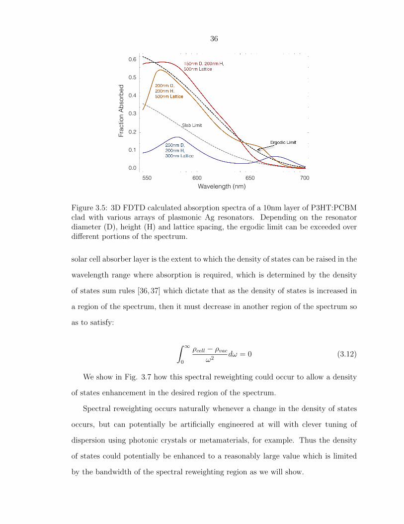
Figure' 3.5:" 3D" FDTD" calculated" absorp3on" spectra" of" a" 10nm" layer" of" P3HT:PCBM"clad" with" various" arrays" of" plasmonic" Ag" resonators." Depending" on" the" resonator"diameter" (D),"height" (H)"and" laIce"spacing," the"ergodic" limit"can"be"exceeded"over"different"por3ons"of"the"spectrum."""
Frac
tion
Abso
rbed
0.6
0.5
0.4
0.3
0.2
0.1
0.0
550 600 650 700 Wavelength (nm)
Figure 3.5: 3D FDTD calculated absorption spectra of a 10nm layer of P3HT:PCBMclad with various arrays of plasmonic Ag resonators. Depending on the resonatordiameter (D), height (H) and lattice spacing, the ergodic limit can be exceeded overdifferent portions of the spectrum.
solar cell absorber layer is the extent to which the density of states can be raised in the
wavelength range where absorption is required, which is determined by the density
of states sum rules [36, 37] which dictate that as the density of states is increased in
a region of the spectrum, then it must decrease in another region of the spectrum so
as to satisfy:
∫ ∞0
ρcell − ρvacω2
dω = 0 (3.12)
We show in Fig. 3.7 how this spectral reweighting could occur to allow a density
of states enhancement in the desired region of the spectrum.
Spectral reweighting occurs naturally whenever a change in the density of states
occurs, but can potentially be artificially engineered at will with clever tuning of
dispersion using photonic crystals or metamaterials, for example. Thus the density
of states could potentially be enhanced to a reasonably large value which is limited
by the bandwidth of the spectral reweighting region as we will show.

37
Figure 3.6: Enhancements needed to absorb the entire solar spectrum. (a) Absorption enhancement over 4n2 (proportional to LDOS enhancement over the homogeneous value) for various thicknesses of Si and GaAs needed to fully absorb the AM1.5 solar spectrum. (b) Needed density of states profiles for two thicknesses of Si needed to fully absorb the spectrum.
Enhancem
ent over
4n
2
Energy (eV)
10 nm GaAs!
100 nm Si!
1000 nm Si!
Density o
f sta
tes (
Ms m
-3)
Energy (eV)
100 nm Si!1000 nm Si!
Homogeneous Si!
a) b)
Figure 3.6: LDOS Enhancements needed to absorb the entire solar spectrum. (a)Absorption enhancement over 4n2 (proportional to LDOS enhancement over the ho-mogeneous value) for various thicknesses of Si and GaAs needed to fully absorb theAM1.5 solar spectrum. (b) Needed density of states profiles for two thicknesses of Sineeded to fully absorb the spectrum.
For a solar of material index n, absorption coefficient α, and thickness x, the
density of states need to absorb all of the incident radiation is given by:
ρmax =ρbulk
1− e−α(4n2)x(3.13)
where ρbulk = n3ω2
π2c3is the homogeneous density of density of states of the bulk
material.
If the cell is to absorb all of the incident light over the spectral range from ω0
to ω1, e.g. over the solar spectrum, then over this range, ρcell → ρmax. By the sum
rule, over some other spectral range, ω2 to ω3, the density of states of the cell must
be reduced. If n and alpha are approximately constant over the range ω0 to ω1 and
n is constant over ω2 to ω3, then the minimum bandwidth of the suppression region,
ω3 − ω2, corresponds to:
(ω3 − ω2) =(ω1 − ω0)
e−α(4n2)x − 1(3.14)
Since the bandwidth of needed enhancement is limited (i.e. the solar spectrum)
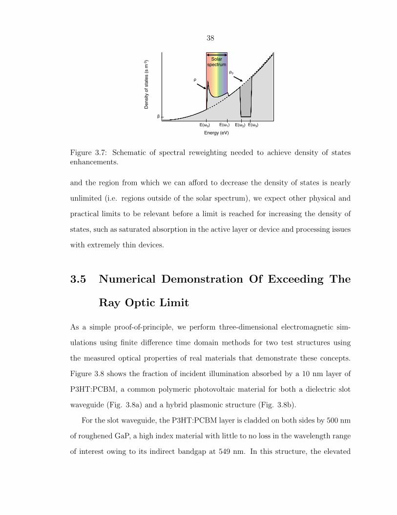
38
E(!2)" E(!3)"E(!0)" E(!1)"
#"
$0"
$"
Energy (eV)"
Density o
f sta
tes (
s m
-3)"
a!
b!
c!
10 nm GaAs"
100 nm Si"
1000 nm Si"
100 nm Si"1000 nm Si"
Homogeneous Si"
Solar spectrum"
Figure 3.7: Schematic of spectral reweighting needed to achieve density of states enhancements.
Figure 3.7: Schematic of spectral reweighting needed to achieve density of statesenhancements.
and the region from which we can afford to decrease the density of states is nearly
unlimited (i.e. regions outside of the solar spectrum), we expect other physical and
practical limits to be relevant before a limit is reached for increasing the density of
states, such as saturated absorption in the active layer or device and processing issues
with extremely thin devices.
3.5 Numerical Demonstration Of Exceeding The
Ray Optic Limit
As a simple proof-of-principle, we perform three-dimensional electromagnetic sim-
ulations using finite difference time domain methods for two test structures using
the measured optical properties of real materials that demonstrate these concepts.
Figure 3.8 shows the fraction of incident illumination absorbed by a 10 nm layer of
P3HT:PCBM, a common polymeric photovoltaic material for both a dielectric slot
waveguide (Fig. 3.8a) and a hybrid plasmonic structure (Fig. 3.8b).
For the slot waveguide, the P3HT:PCBM layer is cladded on both sides by 500 nm
of roughened GaP, a high index material with little to no loss in the wavelength range
of interest owing to its indirect bandgap at 549 nm. In this structure, the elevated

39
Figure 3.8: Full$wave)simula-ons)of)a)P3HT:PCBM)structure)cladded)with:)a,)roughened)GaP)or)b,)plasmonic)resonators)with)absorp-on)enhancement)exceeding)the)ergodic)limit.)The)absorp-on)greatly)exceeds)the)LDOS)limit)for)the)slab)of)P3HT:PCBM)in)air)(dashed)orange)line))and)approach)the)LDOS)limit)for)the)P3HT:PCBM)slot)(dashed)blue)line))with)refined)incoupling.)
LDOS limit!
FDTD simulation!
Ergodic limit!
Slab in air!
LDOS limit!
FDTD simulation!
Ergodic limit!
Slab in air!
!"#$%!&'()
*+!)
*+!)
a!
b!
!"#$%!&'()
,-../.)
01)
0.7
0.6
0.5
0.4
0.3
0.2
0.1
0.0 560 600 640 680
Wavelength (nm) 560 600 640 680 Wavelength (nm)
Frac
tion
Abso
rbed
0.8
0.6
0.4
0.2
0.0
Frac
tion
Abso
rbed
a) b)
Figure 3.8: Full-wave simulations of a P3HT:PCBM structure cladded with roughenedGaP (a) without and (b) with a back reflector that exceeds the ergodic limit. Theabsorption greatly exceeds the LDOS limit for the slab of P3HT:PCBM in air (dashedorange line) and approach the LDOS limit for the P3HT:PCBM slot (dashed blueline) with refined incoupling.
LDOS leads to an enhancement of the absorption that exceeds the ray optic light
trapping limit even without full population of all of the modes of the structure at all
wavelengths where the GaP cladding is transparent. This structure exceeds both the
4n2 and 2n2 limits for absorption enhancement, with and without a back reflector,
respectively. Ideally, Lambertian scattering surfaces could be designed to allow more
nearly equal incoupling to all of the modes, which will further enhance the absorption
over the entire range of the spectrum to the new limit shown by the blue dashed line
in Fig. 3.8a. We also calculate the LDOS limit for this slab in air (orange dashed
line), which is exceeded by our simulation for all wavelengths.
The original ergodic limit calculation assumed isotropic illumination. Thus to
truly exceed this limit a given design should have higher absorption when integrated
over all angles. We thus calculate the angular response of the structure in Fig. 3.8 at
two wavelengths to ensure the design truly exceeds the ergodic limit. Fig. 3.9 shows
fraction of light absorbed at 550 and 600 nm as a function of angle of incidence,
averaged over both polarizations. The ergodic limits are also shown for these two

40
wavelengths. The limit is exceeded for most angles for each of the wavelengths,
falling off only at very steep angles as expected. The angle averaged absorbances for
550 nm and 600 nm light are 0.48 and 0.34, respectively, indicating that the ergodic
limit is surpassed with this structure even with isotropic illumination.
Figure 3.9: Angular behavior of the P3HT:PCBM structure that exceeds the ergodiclimit.
Similarly, Fig. 3.10 indicates that plasmonic resonators situated above and below
the absorber layer also enable absorption enhancements that surpass the ergodic limit.
These two examples demonstrate that with proper design of LDOS and incoupling,
the ergodic limit can be exceeded in several different ways.
We have identified the local density of optical states as a key criterion for exceed-
ing the ray optic light trapping limit in solar cells. To exceed the ray optic limit,
the absorber must exhibit a local density of optical states that exceeds that of the
bulk, homogeneous material within the active region of the cell. In addition to this,
the modal spectrum of the device must be appreciably populated by an appropriate
incoupling mechanism. We have outlined a portfolio of solar absorber designs that
can meet the LDOS criterion implemented utilizing plasmonic materials, dielectric
waveguides, photonic crystals, and resonant optical antennas, and examples are given
to show that incouplers can be designed that provide appreciable mode population.

41
Figure 3.9: Full$wave)simula-ons)of)a)P3HT:PCBM)structure)cladded)with)plasmonic)resonators)that)exceeds)the)ergodic)limit.)
LDOS limit!
FDTD simulation!
Ergodic limit!
Slab in air!
LDOS limit!
FDTD simulation!
Ergodic limit!
Slab in air!
!"#$%!&'()
*+!)
*+!)
a!
b!
!"#$%!&'()
,-../.)
01)
560 600 640 680 Wavelength (nm)
0.8
0.6
0.4
0.2
0.0
Frac
tion
Abso
rbed
Figure 3.10: Full-wave simulations of a P3HT:PCBM structure cladded with plas-monic resonators with absorption enhancement exceeding the ergodic limit.
These concepts and design criteria open the door to design of a new generation of
nanophotonic solar cells that have potential to achieve unprecedented light trapping
enhancements and efficiencies.
3.6 Planar Waveguide Formulation for Exceeding
The Ray Optic Limit
If we limit the scope of the previous section and consider only thin absorbing slabs
(thickness, h ∼ λ) that contain propagating modes, we can describe light trapping
limits by extending a method initially developed by Stuart and Hall [30]. By consid-
ering the reduction in the number of photonic modes in an absorbing slab as the slabs
thickness is reduced, they concluded that the maximum absorption enhancement is
reduced below 4n2.
Despite the early work suggesting that the absorption enhancement in thin slabs
is less than 4n2, recent work has shown that the enhancement may in fact exceed
this limit through the use of photonic crystals [38], plasmonic waveguides [39], high

42
index claddings [25, 26], or an elevation of the local density of optical states [40].
Here we revisit the case of a thin waveguide and determine that the 4n2 limit can be
exceeded for a number of structures that support large propagation constants and/or
slow modal group velocities.
We follow a formalism similar to Refs [30,39] and consider the thermal occupation
of electromagnetic modes in a waveguide surrounded by vacuum. The total density
of modes per unit volume and frequency is given by [30]:
ρtot = ρrad + ρm (3.15)
where
ρrad =
(1−
√1− 1
n2sc
)(n3scω
2
π2c3
)(3.16)
is the density of radiation modes not trapped by total internal reflection within a
material of index nsc, and
ρm =β
2πhvmg(3.17)
is the density of waveguide modes with modal propagation constants βm and group
velocities vmg . Assuming that the modes of the structure are equally occupied from an
appropriate incoupler, the total fraction of incident light absorbed by the film is [39]:
Ftot =ρradρtot
frad +∑m
ρmρtot
fm (3.18)
where
frad =α
α + 1
4
(ρtotv
radg
ρ0v0g
)h
(3.19)

43
and
frad =αΓm
αΓm + 1
4
(ρtotv
radg
ρ0v0g
)h
(3.20)
α is the attenuation coefficient, Γm is modal confinement factor, ρ0 = n3scω
2
π2c3is the
bulk density of states in vacuum, and v0g = c is the speed of light in the surrounding
vacuum. We note that the ratios of the density of states gives the fraction of light
that enters each mode and frad and fm give the rate of absorption divided by the
total rate of energy loss (absorption and out coupling).
We now consider the case of a thin waveguide that only supports one guided
mode. For this case ρrad << ρm, and the total fraction of light absorbed can be
approximated by:
f1−m =αΓm
αΓm + 1
4
(ρtotv
radg
ρ0v0g
)h
=αΓm
αΓm + 1
4
(βmπc3
2ω2hvmg nsc
)h
(3.21)
which can be compared to the fraction of light absorbed in the traditional 4n2
limit [41]:
F4n2 =α
α− 14n2sch
(3.22)
In order to exceed the 4n2 limit, F1−m must be greater than F4n2 . With the
condition F1−m > F4n2 , we obtain our central result:
(βmk0
)(vradg
vmg
)Γm > 4nsc
(h
λ
)(3.23)
Thus in order to surpass the 4n2 limit, we want well-confined modes (Γm ∼ 1)
that have large propagation constants (βm > k0), small group velocities (vmg < vradg ),
and waveguide thicknesses that are small compared to the wavelength of the incident

44
light. By comparing Eq. 3.20 and 3.21, we note that the path length enhancement
lpath is:
lpath =
(c
vmg
)(βmk0
)(h
λ
)Γm (3.24)
Note that the actual path length is lpathh for the single mode waveguide case
compared to 4n2h for the traditional limit.
For a given waveguide structure, the dispersion relation is calculation to determine
the modal parameters needed for Eq. 3.23. Figure 3.11 shows the dispersion relation
for several structures based on a thin film of P3HT:PCBM, a common polymer solar
cell blend. The propagation constants are obtained from the x-axis, and the slopes of
the curves are proportional to the group velocities. Traditional photonic modes for
the slab are confined to the region between the vacuum light line and the absorber
light line (light blue region). In this region, βm < k0, vmg > vradg , and Γm << 1 when
the waveguide is thin. Thus, these photonic slab modes cannot surpass the 4n2 limit.
Figure 3.11: Waveguide dispersion relations. Plasmonic (solid red), Metal-Insulator-Metal (dashed red), and high-low-high index slot (green dashed) waveguides havedispersion relations that lie to the right of the bulk absorber light line (solid blue),which have large propagation constants, slow group velocities, and are well-confined.

45
Figure 3.11 also shows the dispersion relation for three structures that have large
βm, slow vmg , and large confinement factors. These structures include a surface
plasmon polariton waveguide, a high-low-high index dielectric slot waveguide, and
a metal-insulator-metal (MIM) waveguide. These dispersion curves represent the
lowest order TM modes for the structures; however, higher order modes may exist
depending on the thickness of the slab. While Eq. 3.23 is strictly valid only for a
single, highly confined mode, the behavior of the fundamental mode typically dictates
the absorption characteristics, as we shall see below.
A thin surface plasmon polariton waveguide (Fig. 3.12) satisfies the necessary
conditions to surpass the 4n2 limit for a variety of wavelengths and slab thicknesses.
Using Eq. 3.23, we find that the path length enhancement should exceed 4n2 for
absorber thicknesses between 50-105 nm. However, the condition of only one well-
confined mode in the structure is not met for thicknesses larger than 70 nm, because a
second mode exists for larger slab thicknesses. Further, below 50 nm, the confinement
factor is reduced. Figure 3.12a shows the actual absorption enhancement beyond
4n2 for λ=580 nm using Eq. 3.21, which takes into account both propagating and
radiation modes. This structure surpasses the 4n2 limit for the entire range. The
wavelength resolved absorption for a 50 nm thick slab of P3HT:PCBM on Ag is
shown in Fig. 3.11b.
A high-low-high index dielectric slot waveguide is also found to exceed the 4n2
limit. This structure consists of a 10 nm P3HT:PCBM layer cladded on both sides
by a 45 nm layer of GaP, a wide bandgap semiconductor with an indirect energy gap
whose absorption is negligible over the wavelength region of consideration and whose
real part of the refractive index exceeds that of P3HT:PCBM. This structure supports
multiple modes; however we can use our expression for the path length enhancement
to predict whether or not the structure could surpass the 4n2 limit if only one mode
were present. Figure 3.13a shows that the lowest order TE and TM modes for =580
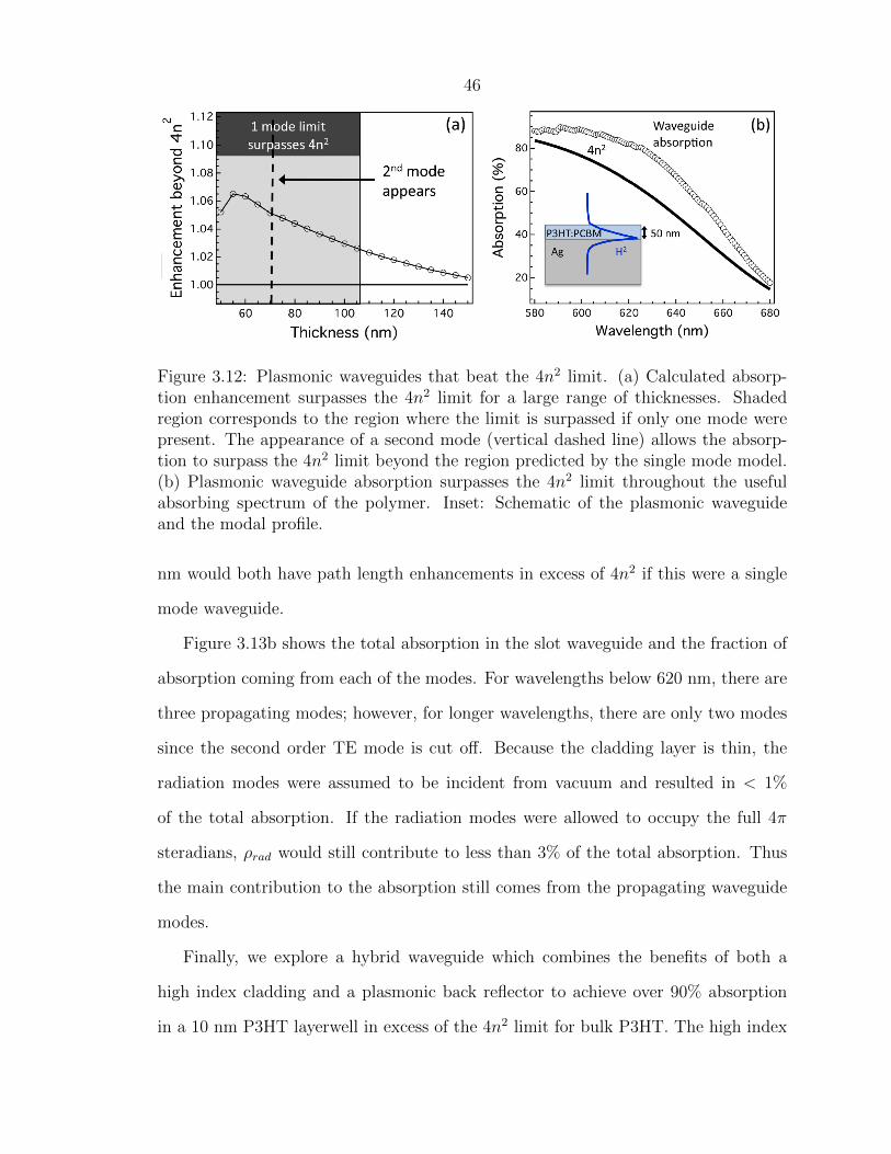
46
Figure 3.12: Plasmonic waveguides that beat the 4n2 limit. (a) Calculated absorp-tion enhancement surpasses the 4n2 limit for a large range of thicknesses. Shadedregion corresponds to the region where the limit is surpassed if only one mode werepresent. The appearance of a second mode (vertical dashed line) allows the absorp-tion to surpass the 4n2 limit beyond the region predicted by the single mode model.(b) Plasmonic waveguide absorption surpasses the 4n2 limit throughout the usefulabsorbing spectrum of the polymer. Inset: Schematic of the plasmonic waveguideand the modal profile.
nm would both have path length enhancements in excess of 4n2 if this were a single
mode waveguide.
Figure 3.13b shows the total absorption in the slot waveguide and the fraction of
absorption coming from each of the modes. For wavelengths below 620 nm, there are
three propagating modes; however, for longer wavelengths, there are only two modes
since the second order TE mode is cut off. Because the cladding layer is thin, the
radiation modes were assumed to be incident from vacuum and resulted in < 1%
of the total absorption. If the radiation modes were allowed to occupy the full 4π
steradians, ρrad would still contribute to less than 3% of the total absorption. Thus
the main contribution to the absorption still comes from the propagating waveguide
modes.
Finally, we explore a hybrid waveguide which combines the benefits of both a
high index cladding and a plasmonic back reflector to achieve over 90% absorption
in a 10 nm P3HT layerwell in excess of the 4n2 limit for bulk P3HT. The high index

47
Figure 3.13: Slot waveguides that beat the 4n2 limit. (a) Path length enhancement ifonly one mode were present. Both the lowest TM and TE modes surpass 4n2. Insets:Mode profiles. (b) Modal decomposition of the absorbed fraction of the incident light.The total absorption surpasses the 4n2 limit. Inset: Schematic of the high-low-highindex slot waveguide.
GaP cladding further confines the mode and reduces its group velocity. Figure 3.14
shows the total waveguide absorption, the absorption expected for 4n2 passes, and
the absorption obtained by a 10 nm thick P3HT film surrounded by vacuum. Note
that the 10 nm thick P3HT film in vacuum has a significantly lower absorption than
would be expected by the 4n2 limit. This is due to the fact that the photonic modes
are not well confined, have higher group velocities than do modes in the bulk, and
have small propagation constants, which are in agreement with the conclusions of
Ref. [30].
In summary, we have described a general method for predicting whether or not
thin waveguides can have absorption enhancements in excess of the 4n2 limit based on
their dispersion relations. We gave several examples of such structures by including
plasmonic back reflectors and/or high index claddings in order to manipulate the
modal propagation constant, group velocity, and confinement factor. Our results
provide both a qualitative and quantitative design scheme for improving the light
trapping in thin films, which is highly desired for solar cell applications.

48
Figure 3.14: Absorption for a plasmonic waveguide cladded with a high index (GaP)top layer. Waveguide absorption (circles) is well in excess of the 4n2 limit (solid line)and the calculated absorption for a planar slab in vacuum (dashed line).

49
Chapter 4
Light Trapping With DielectricNanosphere Resonators
We have seen how various nanophotonic elements can act as useful tools to enhance
optical absorption for photovoltaic devices. Here, we will examine in greater detail
the behavior of a simple low cost, low loss scheme for absorption enhancement based
on dielectric nanosphere resonators. The resonators can act as both scattering centers
or as diffractive elements that change the momentum of incident photons and enables
access of trapped modes in the absorbing layer. The periodic arrangement of the
resonators allows for great flexibility for optical dispersion engineering and tuning of
optical absorption for different materials applications. Here we show how this simple
scheme can be applied to both traditional a-Si solar cell designs, as well as current
thin-film GaAs solar cells. While neither of the two cases discusses here exceed the
ergodic light tapping limit, further investigation with higher index resonators could
potentially achieve this.
50
4.1 Dielectric Nanosphere Resonators for a-Si Ab-
sorption Enhancement
We propose here a light trapping configuration for a-Si solar cells based on coupling
from a periodic arrangement of resonant dielectric nanospheres. It is shown that
photonic modes in the spheres can be coupled into particular modes of the solar cell
and significantly enhance its efficiency. We numerically demonstrate this enhancement
using full field finite difference time domain (FDTD) simulations of a nanosphere array
above a typical thin film amorphous silicon (a-Si) solar cell structure. The incoupling
element in this design is advantageous over other schemes as it is composed of a lossless
material and its spherical symmetry naturally accepts large angles of incidence. Also,
the array can be fabricated using simple, well developed methods of self assembly and
is easily scalable without the need for lithography or patterning. This concept can be
easily extended to many other thin film solar cell materials to enhance photocurrent
and angular sensitivity.
Thin film photovoltaics offer the potential for a significant cost reduction [11]
compared to traditional, or first generation photovoltaics usually at the expense of
high efficiency. This is achieved mainly by the use of amorphous or polycrystalline
optoelectronic materials for the active region of the device, for example, a-Si. The
resulting carrier collection efficiencies, operating voltages, and fill factors are typically
lower than for single crystal cells, which reduce the overall cell efficiency. There is thus
great interest in using thinner active layers combined with advanced light trapping
schemes to minimize these problems and maximize efficiency.
Wavelength-scale dielectric spheres [42] are interesting photonic elements because
they can diffractively couple light from free space and also support confined resonant
modes. Moreover, the periodic arrangement of nanospheres can lead to coupling
between the spheres, resulting in mode splitting and rich bandstructure [43,44]. The
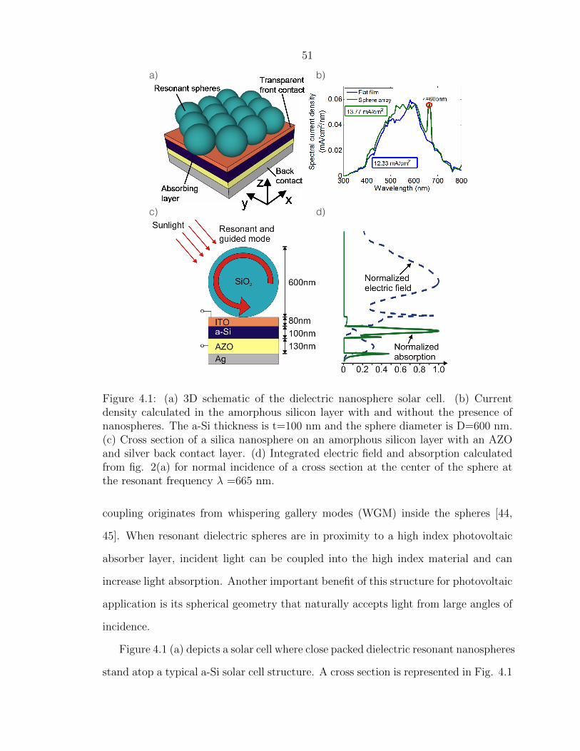
51
Figure'4.1:"(a)"3D"schema-c"of"the"dielectric"nanosphere"solar"cell."(b)"Current"density"calculated"in"the"amorphous"silicon"layer"with"and"without"the"presence"of"nanospheres."The"a>Si"thickness"is"t=100"nm"and"the"sphere"diameter"is"D=600"nm."(c)"Cross"sec-on"of"a"silica"nanosphere"on"an"amorphous"silicon"layer"with"an"AZO"and"silver"back"contact"layer."(d)"Integrated"electric"field"and"absorp-on"calculated"from"fig."2(a)"for"normal"incidence"of"a"cross"sec-on"at"the"center"of"the"sphere"at"the"resonant"frequency"λ=665"nm.""
!
a) b)
c) d)
Figure 4.1: (a) 3D schematic of the dielectric nanosphere solar cell. (b) Currentdensity calculated in the amorphous silicon layer with and without the presence ofnanospheres. The a-Si thickness is t=100 nm and the sphere diameter is D=600 nm.(c) Cross section of a silica nanosphere on an amorphous silicon layer with an AZOand silver back contact layer. (d) Integrated electric field and absorption calculatedfrom fig. 2(a) for normal incidence of a cross section at the center of the sphere atthe resonant frequency λ =665 nm.
coupling originates from whispering gallery modes (WGM) inside the spheres [44,
45]. When resonant dielectric spheres are in proximity to a high index photovoltaic
absorber layer, incident light can be coupled into the high index material and can
increase light absorption. Another important benefit of this structure for photovoltaic
application is its spherical geometry that naturally accepts light from large angles of
incidence.
Figure 4.1 (a) depicts a solar cell where close packed dielectric resonant nanospheres
stand atop a typical a-Si solar cell structure. A cross section is represented in Fig. 4.1

52
(c). We use a silver back contact and, in order to avoid diffusion between the silver
layer and the a-Si layer, a 130 nm aluminium-doped zinc oxide (AZO) layer is placed
between the silver and the a-Si layer [46]. An 80 nm indium tin oxide (ITO) layer
is used as a transparent conducting front contact and also acts as an anti-reflection
coating. 600 nm diameter silica nanospheres with a refractive index of n=1.46 are
directly placed on the ITO as a hexagonally close packed monolayer array.
Figure'4.2:"(a)"Electric"field"intensity"for"a"cross"sec4on"at"the"middle"of"a"sphere"in"the"(x,z)"plane"at"λ=665"nm."Below"is"a"zoom"of"the"aBSi"layer."The"direc4on"of"the"electric"field"of"the"incident"plane"wave"is"also"represented."(b,c)"Ey"component"of"the"electric"field"from"a"cross"sec4on"in"the"(x,y)"plane"in"the"middle"of"the"aBSi"layer."(d,e,f)"Same"as"(a,b,c)"for"λ="747"nm"which"corresponds"to"a"frequency"off"resonance.""
!
a) b) c)
d) e) f)
Figure 4.2: (a) Electric field intensity for a cross section at the middle of a spherein the (x,z) plane at λ=665 nm. Below is a zoom of the a-Si layer. The direction ofthe electric field of the incident plane wave is also represented. (b,c) Ey componentof the electric field from a cross section in the (x,y) plane in the middle of the a-Silayer. (d,e,f) Same as (a,b,c) for λ= 747 nm which corresponds to a frequency offresonance.
In order to study the response of the system, we perform three-dimensional full

53
field electromagnetic simulations to determine the expected absorption enhancement
compared to a-Si absorbers without a layer of dielectric spheres. A broadband wave
pulse with the electric field polarized along the x axis [see Fig. 4.1(a)] is injected at
normal incidence on the structure, and the fields are monitored at 100 wavelengths
equally spaced between λ=300 nm and λ=800 nm. This wavelength range corresponds
to the suns energy spectrum below the bandgap of a-Si. In order to determine how
much current can be generated from the structure, we calculate the optical generation
rate in the silicon by [47]:
Gnopt(ω) =
∫ε′′(ω)|E(ω)|2s
2hΓsolar(ω)dV (4.1)
where ε′′
is the imaginary part of the dielectric function of the silicon and |E(ω)|2
is the electric field intensity integrated over the simulation volume containing the
amorphous silicon [48]. If all electrons generated are collected, this will correspond to
the device’s short circuit current. Γsolar is a factor used to weight each wavelength by
the AM1.5 solar spectrum. In Fig. 4.1 (d), we plot the normalized integrated electric
field and absorption of a cross section at the center of the sphere perpendicular to the
incoming plane wave and in the plane of the electric field for the resonant frequency
λ=665 nm. The absorption is proportional to ε′′ |E(ω)|2s as shown is Eq. 4.1.
To compare the influence of the spheres on the solar cell structure presented in Fig.
4.1 (a), we calculate the spectral current density in the a-Si layer with and without
the presence of 600 nm diameter nanospheres. The result is presented on Fig. 4.1
(b). The overall integrated current density corresponding to the energy absorbed in
the a-Si in the presence of the nanospheres is J=13.77 mAcm2 , which corresponds to an
enhancement of 12% compared to the case without the sphere array. Over almost the
entire wavelength range, the spectral current density is higher with the spheres than
without the spheres, while the narrow band response is due to a coupling between the
spheres and the solar cell. Furthermore, there exists discrete enhancements at specific

54
wavelengths. The broadband enhancement can be explained by the spheres acting as
an anti-reflection coating. At λ=665 nm, the enhancement is greater than 100%. To
explain this increase in the current density, we plot in Fig. 4.2 (a) the electric field
intensity for a cross section in the middle of a sphere in the (x,z) plane. Two lobes
are observed on each side of the sphere. These are characteristic of WGMs. They
have significant field strength within the periodic arrangement of the sphere layer.
The WGMs of the spheres couple with each other due to their proximity [49],
which can lead to waveguide formation [43].
We represent in Fig. 4.2 (b) and (c) the Ey component of the electric field for
a cross section in the (x,y) plane in the middle of the a-Si layer. The observed
field profile is periodic and oscillates in phase with the period. Because the sphere
array by itself has very low loss, the mode energy eventually gets absorbed into the
a-Si and increases the generated photocurrent. In Fig. 4.2 (c), we show the Ey
component of the electric field, corresponding to a TE guided mode along the x axis.
There also exists a TM guided mode of the same periodicity that contributes to the
enhancement of the absorption at λ=665 nm (not shown). As a comparison, we show
in Fig. 4.2 (d,e,f) an equivalent analysis, off resonance at λ=747 nm. Clearly there
is no resonance in the sphere and no excitation of a guided mode at this wavelength.
The spherical shape of the structure above the solar cell also enables incoupling
at large angles of incidence. In order to verify this, we compared the absorbed light
at normal incidence and at 20 and 40 angle to the normal in both TE and TM
polarizations. For simplicity, we considered only an array of silica spheres above
a 100 nm a-Si layer. Figure 4.3 (a) and (d) show a schematic of the simulated
structures without and with silica spheres on top of the a-Si. Figure 4.3 (b), (c),
(e) and (f) correspond to the spectral current density in the a-Si for both cases
without and with silica spheres respectively, and for TE and TM polarizations. For
normal incidence, the calculated improvement is 29.6% and is independant from the

55
polarization. This high improvement compared to the solar cell previously described
can be explained by the absence of an antireflection coating layer and back reflector
layer in this simplified case. For TM polarization, the improvement is 13.8% for 20
and 3.9% for 40 incidence angle. For TE polarization, the improvement compared
to a flat layer remains around 29% for all angles. However, in the case of a TM
polarization, for a flat a-Si film, the larger the angle, the larger the energy absorbed.
That is why the current improvement of a structure with spheres decreases over that
of a structure without spheres in the case of a TM-polarized plane wave.
Figure'4.3:"(a)"Schema+c"of"the"flat"case"model"with"an"angle"and"spectral"current"density"in"(b)"TE"and"(c)"TM"polariza+on."(d)"Schema+c"of"the"case"with"nanospheres"on"top"and"spectral"current"density"in"(e)"TE"and"(f)"TM"polariza+on."(g)"Top"view"of"the"periodic"arrangement"of"the"nanospheres"with"a"large"laBce"constant."The"rectangle"indicates"the"periodicity"used"for"numerical"simula+ons."(h)"Current"density"for"three"different"sphere"spacings"where"an"efficient"coupling"between"the"spheres"exists."(i)"Current"density"for"a"flat"cell"and"with"a"rela+vely"large"distance"between"the"spheres.""
!
a) b) c)
d) e) f)
g) h) i)
Figure 4.3: (a) Schematic of the flat case model with an angle and spectral currentdensity in (b) TE and (c) TM polarization. (d) Schematic of the case with nanosphereson top and spectral current density in (e) TE and (f) TM polarization. (g) Topview of the periodic arrangement of the nanospheres with a large lattice constant.The rectangle indicates the periodicity used for numerical simulations. (h) Currentdensity for three different sphere spacings where an efficient coupling between thespheres exists. (i) Current density for a flat cell and with a relatively large distancebetween the spheres.
As the lattice constant of the hexagonal array of spheres varies, as represented in

56
Fig. 4.3 (g), the efficiency of the WGM guided wave changes due to different coupling
conditions between the spheres. In Fig. 4.3 (h), we show the spectral current density
for different spacings between the spheres. The peak at λ=665 nm for close packed
spheres is shifted to longer wavelengths as the distance between the spheres increases.
This provides evidence that the incoupling is due to a diffractive mechanism. For
Λ=650 nm and Λ=700 nm, a second peak appears at λ=747 nm and λ=780 nm,
respectively. This corresponds to an optimal coupling condition between the WGM
and the a-Si waveguide mode for these specific periodicities and wavelengths. For the
considered design, a separation of Λ=700 nm gives the highest current density with
J=14.14 mAcm2 which represents an enhancement of 15% compared to a flat a-Si cell with
antireflection coating. As shown on Fig. 4.3 (i), when Λ > 1000 nm, the coupling
between the spheres almost disappears and the enhancement significantly decreases.
From an experimental point-of-view, a close packed configuration is more feasible
than a hexagonal one. However, the spacing between spheres could be varied by an
additional coating on each sphere or by assembly on photolithographically patterned
substrates [50]. An intriguing aspect of changing the spacing between the spheres is
that it allows one to tune and adjust which wavelengths are coupled into the solar
cell. This, coupled with the option of using different sphere sizes in a single array
could potentially allow for broadband enhancement.
In order to estimate the influence of the sphere diameter on the enhancement of
the solar cell efficiency, we represent on fig. 4.4 the ratio between the spectral current
density of a solar cell with close packed spheres over the spectral current density of
a solar cell without spheres. The sphere diameter varies between D=100 nm and
D=1000 nm. We can observe a general broadened enhancement due to the additional
anti-reflection coating made by the spheres. Moreover, strong discrete enhancement
lines also appear. These correspond to the WGMs at certain wavelengths. Since the
a-Si absorption becomes weaker over λ= 600 nm, the enhancement corresponding to
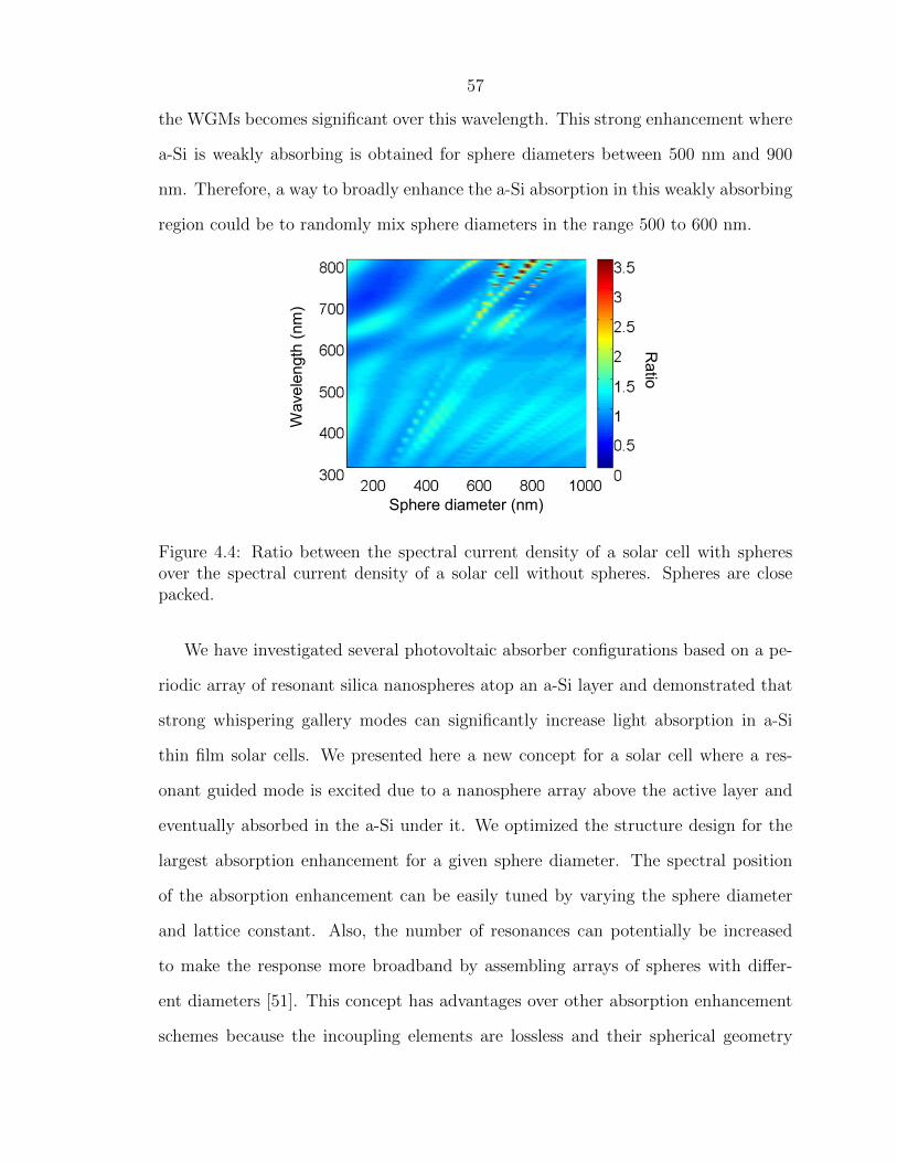
57
the WGMs becomes significant over this wavelength. This strong enhancement where
a-Si is weakly absorbing is obtained for sphere diameters between 500 nm and 900
nm. Therefore, a way to broadly enhance the a-Si absorption in this weakly absorbing
region could be to randomly mix sphere diameters in the range 500 to 600 nm.
Figure'4.4:"(a)"Ra'o"between"the"spectral"current"density"of"a"solar"cell"with"spheres"over"the"spectral"current"density"of"a"solar"cell"without"spheres."Spheres"are"close"packed."""
Sphere diameter (nm)
Ratio
Wav
elen
gth
(nm
)
Figure 4.4: Ratio between the spectral current density of a solar cell with spheresover the spectral current density of a solar cell without spheres. Spheres are closepacked.
We have investigated several photovoltaic absorber configurations based on a pe-
riodic array of resonant silica nanospheres atop an a-Si layer and demonstrated that
strong whispering gallery modes can significantly increase light absorption in a-Si
thin film solar cells. We presented here a new concept for a solar cell where a res-
onant guided mode is excited due to a nanosphere array above the active layer and
eventually absorbed in the a-Si under it. We optimized the structure design for the
largest absorption enhancement for a given sphere diameter. The spectral position
of the absorption enhancement can be easily tuned by varying the sphere diameter
and lattice constant. Also, the number of resonances can potentially be increased
to make the response more broadband by assembling arrays of spheres with differ-
ent diameters [51]. This concept has advantages over other absorption enhancement
schemes because the incoupling elements are lossless and their spherical geometry

58
allows light to be efficiently coupled into the solar cell over a large range of incident
angles. Also these arrays can be fabricated and easily scaled using standard self as-
sembly [45, 52] techniques without the need for lithography. In addition to this, the
presented enhancement results are performed on a totally flat a-Si layer which has an
advantage over cells grown on textured surfaces as surface roughness or topography
can create holes, oxidation and thus reduce the efficiency and lifetime of the solar
cell. The sphere array can also be easily integrated or combined with existing absorp-
tion enhancement techniques. This light trapping concept offers great flexibility and
tunability and can be extended for use with many other thin film solar cell materials.
4.2 Dielectric Nanosphere Resonators for GaAs Ab-
sorption Enhancement
The route to more than 30% single junction solar cell efficiency requires the short
circuit current Jsc, the open circuit voltage Voc, and the fill factor FF to be near their
theoretical maximum values. The current single junction solar cell record at 1 sun
illumination is 28.2% [15], which is for a GaAs cell. While it is unclear whether the
current losses are from absorption or collection, investigating all optical methods to
maximize the absorption is of great importance. Additionally, reducing the amount of
material is necessary for reducing both the cost and weight of the cell, which requires
advanced light trapping strategies as the active layer thinned [11].
Thin film photovoltaics offer the possibility to significantly reduce the cost of a
solar cell compared to first generation solar cells, usually at the expense of efficiency. It
is therefore of great interest to combine thin film absorbing layers with advanced light
trapping schemes to reduce the cost without reducing the efficiency. Light trapping
is a critical requirement in thin film photovoltaics, and dielectric texturing is a viable
method to induce light trapping [19], but for some materials thin film device quality
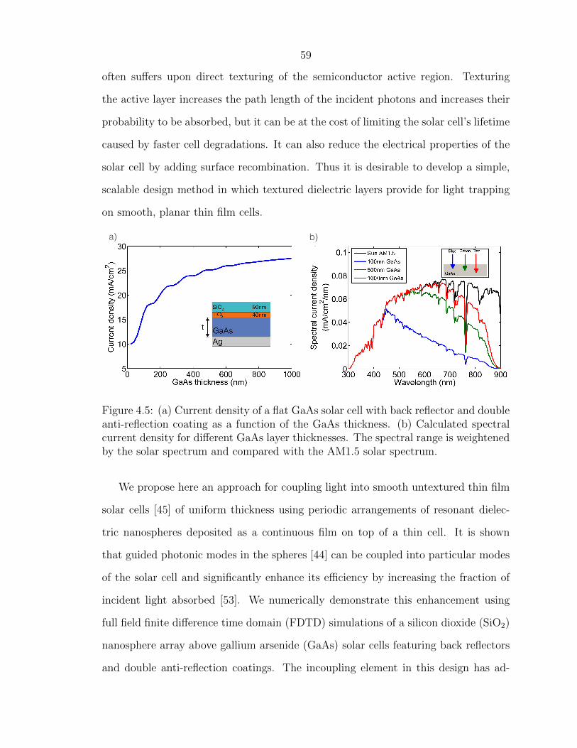
59
often suffers upon direct texturing of the semiconductor active region. Texturing
the active layer increases the path length of the incident photons and increases their
probability to be absorbed, but it can be at the cost of limiting the solar cell’s lifetime
caused by faster cell degradations. It can also reduce the electrical properties of the
solar cell by adding surface recombination. Thus it is desirable to develop a simple,
scalable design method in which textured dielectric layers provide for light trapping
on smooth, planar thin film cells.
Figure'4.5:"(a)"Current"density"of"a"flat"GaAs"solar"cell"with"back"reflector"and"double"an;<reflec;on"coa;ng"as"a"func;on"of"the"GaAs"thickness."(b)"Calculated"spectral"current"density"for"different"GaAs"layer"thicknesses."The"spectral"range"is"weightened"by"the"solar"spectrum"and"compared"with"the"AM1.5"solar"spectrum.""
!
!
a) b)
Figure 4.5: (a) Current density of a flat GaAs solar cell with back reflector and doubleanti-reflection coating as a function of the GaAs thickness. (b) Calculated spectralcurrent density for different GaAs layer thicknesses. The spectral range is weightenedby the solar spectrum and compared with the AM1.5 solar spectrum.
We propose here an approach for coupling light into smooth untextured thin film
solar cells [45] of uniform thickness using periodic arrangements of resonant dielec-
tric nanospheres deposited as a continuous film on top of a thin cell. It is shown
that guided photonic modes in the spheres [44] can be coupled into particular modes
of the solar cell and significantly enhance its efficiency by increasing the fraction of
incident light absorbed [53]. We numerically demonstrate this enhancement using
full field finite difference time domain (FDTD) simulations of a silicon dioxide (SiO2)
nanosphere array above gallium arsenide (GaAs) solar cells featuring back reflectors
and double anti-reflection coatings. The incoupling element in this design has ad-
60
vantages over other schemes as it is a lossless dielectric material, and its spherical
symmetry naturally accepts a wide angle of incidence range. Moreover, analytical
models show that for nanospheres of a given dielectric material, a large number of
resonant modes can be supported, which can give rise to a 11% absorption enhance-
ment in a 100 nm thick GaAs absorber layer at several wavelengths between 300 nm
and 900 nm and 2.5% enhancement in the case of a 1000 nm thick GaAs absorber
layer. Also, the SiO2 nanosphere array can be fabricated using simple, well developed
self assembly methods and is easily scalable without the need for lithography or pat-
terning. This concept can be easily extended to other thin film solar cell materials,
such as silicon or copper indium gallium diselenide (CIGS).
We demonstrated previously the use of dielectric nanospheres for solar applications
in the case of a thin film amorphous silicon solar cell [53]. GaAs is the semiconductor
whose absorption is best matched with the solar spectrum [54] and which currently
has the world record for single junction solar cell efficiency at 1 sun illumination [15].
Moreover, it has already widely been investigated in several configurations [55, 56];
therefore, we extend the concept of using dielectric nanospheres to a GaAs solar
cell. We numerically demonstrate the optimal sphere size and spacing to achieve the
highest possible photocurrent density for several thicknesses of GaAs solar cells with
a double antireflection coating and a hexagonally close packed array of silica spheres.
We first consider a GaAs solar cell with a 40 nm thick titanium dioxide (TiO2) and
90 nm thick silicon dioxide (SiO2) double layer antireflection coating and a silver back
reflector. A broadband wave pulse with the electric field polarized along the x-axis
is injected at normal incidence on the structure, and the fields are monitored at 300
wavelengths equally spaced between λ = 300 nm and λ = 900 nm. This wavelength
range corresponds to the sun’s energy spectrum below the bandgap of GaAs. The
optical generation rate in the GaAs is calculated using [48]:

61
Gnopt(ω) =
∫ε′′(ω)|E(ω)|2GaAs
2hΓsolar(ω)dV (4.2)
where |E(ω)|2GaAs is the electric field intensity integrated over the GaAs volume [48]
and ε′′
is the imaginary part of the dielectric function of the GaAs. Γsolar is a factor
used to weight each wavelength by the AM1.5 solar spectrum. We represent in Fig.
4.5a the current density of a flat GaAs solar cell with back reflector and double
anti-reflection coating as a function of the GaAs thickness. The current density
considerably increases within the first five hundred nanometers. This shows that
most of the light is absorbed within this range. For a 500 nm thick GaAs solar cell,
we calculate a current density of 25.19 mAcm2 . Then, above 500 nm, the current density
slowly increases to reach 27.56 mAcm2 for a 1000 nm thick GaAs solar cell. This value
corresponds to 82% of the maximum attainable value. Even though this value is high,
it still gives potential for improvement.
We present in Fig. 4.5b the AM1.5 solar spectrum and plots that indicate the
fraction of the solar energy absorbed in three thin GaAs layers on a single pass. The
current density is calculated by J = Gnana(ω)e− where e− is the elementary charge
and
Gnana(ω) = α(ω)N0
∫e−α(ω)xdx (4.3)
is the analytically calculated optical generation rate. N0 is the sun photon flux
at the top of the GaAs layer and α(ω) = 4πkλ
where k is the imaginary part of the
refractive index. Figure 4.5b gives us an indication of where in the spectral range there
exists potential for improvement to increase the absorption in a GaAs absorbing layer
for the three considered thicknesses. Clearly, a large fraction of the solar spectrum
is poorly absorbed, especially in the 600 - 900 nm spectral range for the case of a
1000 nm thick GaAs absorbing layer. Thus, a way to increase the absorption in this
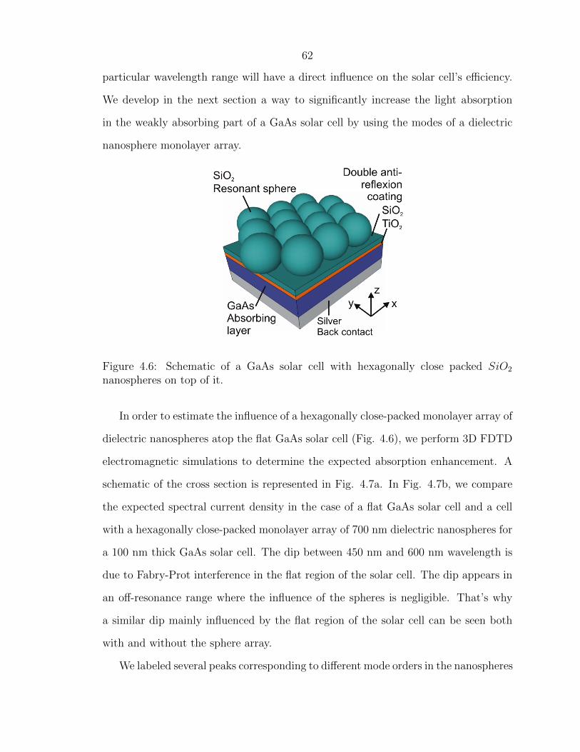
62
particular wavelength range will have a direct influence on the solar cell’s efficiency.
We develop in the next section a way to significantly increase the light absorption
in the weakly absorbing part of a GaAs solar cell by using the modes of a dielectric
nanosphere monolayer array.
Figure'4.5:"(a)"Current"density"of"a"flat"GaAs"solar"cell"with"back"reflector"and"double"an;<reflec;on"coa;ng"as"a"func;on"of"the"GaAs"thickness."(b)"Calculated"spectral"current"density"for"different"GaAs"layer"thicknesses."The"spectral"range"is"weightened"by"the"solar"spectrum"and"compared"with"the"AM1.5"solar"spectrum.""
a) b)
!
Figure 4.6: Schematic of a GaAs solar cell with hexagonally close packed SiO2
nanospheres on top of it.
In order to estimate the influence of a hexagonally close-packed monolayer array of
dielectric nanospheres atop the flat GaAs solar cell (Fig. 4.6), we perform 3D FDTD
electromagnetic simulations to determine the expected absorption enhancement. A
schematic of the cross section is represented in Fig. 4.7a. In Fig. 4.7b, we compare
the expected spectral current density in the case of a flat GaAs solar cell and a cell
with a hexagonally close-packed monolayer array of 700 nm dielectric nanospheres for
a 100 nm thick GaAs solar cell. The dip between 450 nm and 600 nm wavelength is
due to Fabry-Prot interference in the flat region of the solar cell. The dip appears in
an off-resonance range where the influence of the spheres is negligible. That’s why
a similar dip mainly influenced by the flat region of the solar cell can be seen both
with and without the sphere array.
We labeled several peaks corresponding to different mode orders in the nanospheres

63
[45] above the solar cell. For the case represented in Fig. 4.7d, the enhancement due
to the sphere’s whispering gallery mode is more that 300%. Because in the near in-
frared part of the solar spectrum GaAs is weakly absorbing, we are able in this case,
due to the monolayer spheres array, to enhance the generated current density by more
than 11%.
!Figure'4.5:"(a)"Current"density"of"a"flat"GaAs"solar"cell"with"back"reflector"and"double"an;<reflec;on"coa;ng"as"a"func;on"of"the"GaAs"thickness."(b)"Calculated"spectral"current"density"for"different"GaAs"layer"thicknesses."The"spectral"range"is"weightened"by"the"solar"spectrum"and"compared"with"the"AM1.5"solar"spectrum.""
a) b)
c) d) e)
c d
e
Figure 4.7: (a) Cross section of a silica nanosphere on a flat GaAs solar cell withback reflector and double layer anti-reflection coating. (b) Spectral current density ofa 100 nm thick GaAs flat cell and a cell with a hexagonally close-packed monolayerarray of 700 nm diameter dielectric nanospheres. Each peak labeled (c), (d) and (e)correspond to different whispering gallery mode orders where we show the electricfield intensity for a cross section at the middle of a sphere at different wavelengthsfor the labeled peaks. The E field of the initial plane wave is oriented in the (x,z)plane. The black circles show the contour of the sphere.
In Fig. 4.8a, b, c, we illustrate the ratio between the spectral current density of a
solar cell with hexagonally close packed spheres over the spectral current density of a
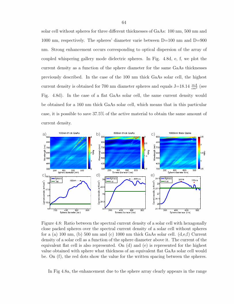
64
solar cell without spheres for three different thicknesses of GaAs: 100 nm, 500 nm and
1000 nm, respectively. The spheres’ diameter varie between D=100 nm and D=900
nm. Strong enhancement occurs corresponding to optical dispersion of the array of
coupled whispering gallery mode dielectric spheres. In Fig. 4.8d, e, f, we plot the
current density as a function of the sphere diameter for the same GaAs thicknesses
previously described. In the case of the 100 nm thick GaAs solar cell, the highest
current density is obtained for 700 nm diameter spheres and equals J=18.14 mAcm2 (see
Fig. 4.8d). In the case of a flat GaAs solar cell, the same current density would
be obtained for a 160 nm thick GaAs solar cell, which means that in this particular
case, it is possible to save 37.5% of the active material to obtain the same amount of
current density.
!
Figure'4.5:"(a)"Current"density"of"a"flat"GaAs"solar"cell"with"back"reflector"and"double"an;<reflec;on"coa;ng"as"a"func;on"of"the"GaAs"thickness."(b)"Calculated"spectral"current"density"for"different"GaAs"layer"thicknesses."The"spectral"range"is"weightened"by"the"solar"spectrum"and"compared"with"the"AM1.5"solar"spectrum.""
a) b) c)
c) d) e)
Figure 4.8: Ratio between the spectral current density of a solar cell with hexagonallyclose packed spheres over the spectral current density of a solar cell without spheresfor a (a) 100 nm, (b) 500 nm and (c) 1000 nm thick GaAs solar cell. (d,e,f) Currentdensity of a solar cell as a function of the sphere diameter above it. The current of theequivalent flat cell is also represented. On (d) and (e) is represented for the highestvalue obtained with sphere what thickness of an equivalent flat GaAs solar cell wouldbe. On (f), the red dots show the value for the written spacing between the spheres.
In Fig 4.8a, the enhancement due to the sphere array clearly appears in the range

65
between 700 nm and 900 nm wavelength where the enhancement lines directly refer to
the mode orders. In the case of the 500 nm thick GaAs solar cell, the highest current
density is obtained with 500 nm diameter hexagonally close packed nanospheres on
top of it and equals J=26.00 mAcm2 . This corresponds to a 3.2% enhancement compared
to a flat GaAs solar cell with double antireflection coating where the current density
equals J=25.19 mAcm2 . Note that, as shown in fig. 4.8e, in order to obtain the same
current density with a flat GaAs solar cell, we would have need 600 nm of active
material. For the case of the 1000 nm thick GaAs solar cell, the highest current is
obtained for D=500 nm diameter spheres and is equal to J=27.41 mAcm2 (see Fig. 5f).
Some enhancement for subwavelength diameter spheres is also seen, probably due
to scattering effects [42]. There is still room for improvement for each of these cell
thicknesses as the currents are not yet at the maximum attainable value, even for
the 1000 nm thick cell. The current densities can potentially be increased further by
utilizing spheres of multiple diameters, partially embedding the spheres or texturing
the underlying AR coatings. On a given peak resonance, the absorption is also in-
fluenced by the distance between the sphere array and the GaAs layer. Therefore,
there exists an optimal distance between the sphere array and the absorbing layer
which can be tuned for maximizing the absorption related to each independent peaks
due to the sphere modes. However, modifying the distance between the spheres and
the absorbing layer means to modify the double antireflection coating thickness and
potentially degrade the performance of the cell off resonance. If we slightly tune the
spacing between the spheres to a=20 nm, it reaches J=28.23 mAcm2 which corresponds
to an enhancement of 2.5% compared to a flat solar cell with double antireflection
coating. As we can see on Fig. 4.7, the enhancement occurs mainly at wavelength
scale diameter spheres where low order whispering gallery modes occur. In the case
of 740 nm diameter nanospheres, we can show that by tuning the spacing to a=120
nm between the spheres, we can increase the spectral current from J=27.90 mAcm2 for

66
a hexagonally close packed array of nanospheres to J=28.13 mAcm2 . This represents an
enhancement of 2.0% compared to a flat solar cell with double antireflection coating.
While this enhancement is less than shown earlier for the case of the 500 nm diameter
sphere array with 20 nm spacing, a part of the enhancement occurs near the band
edge, which may be beneficial for thin cells. This improvement due to the spacing is
detailed on Fig. 4.9. At λ=870 nm, there exists a mode with an effect that can be
significantly enhanced with the spacing between the nanospheres as it can be seen on
Fig 4.9b. In order to understand this enhancement, we plot on Fig. 4.9c the field
profile of a cross section at the middle of a sphere in the (x,z) plane at λ=870 nm for
a hexagonally close packed array of nanospheres and compare it with the case where
the spheres are a=120 nm away from each other. It appears that this separation
results in a greater coupling between the array of spheres and the active material.
This is most likely due to a better coupling between the spheres themselves as the
field profile suggests.
We demonstrated light absorption enhancement on a 100 nm, a 500 nm and a
1000 nm thick GaAs solar cell structure featuring a back reflector, a double layer
anti-reflection coating, and a close packed silica nanosphere array. The thinner the
cell is, the more potential for improvement. We could see the highest improvement of
11% for the 100 nm GaAs solar cell by adding 700 nm hexagonally close packed SiO2
nanospheres on top of it. We could see that depending on the size of the spheres,
the enhancement we obtain occurs on different parts of the spectrum. Therefore, the
best current densities are obtained where nanosphere array modes enhance the weakly
absorbing region of the active material. By optimizing the sphere size and spacing,
we showed an improvement of 2.5% in the current generation for the case of a 1000
nm thick GaAs solar cell. As we also showed the overall absorption enhancement
obtained with thinner absorbing layers, around 100 nm, is much greater. In the case
of a 1000 nm thick GaAs solar cell, because the initial absorption is very high for the
67
considered flat structure, the improvement using a single size nanosphere structure is
much less; however, there is still improvement potential in the range 800 - 900 nm,
leading to total absorbed currents close to the maximum attainable value.

68
!Figure'4.5:"(a)"Current"density"of"a"flat"GaAs"solar"cell"with"back"reflector"and"double"an;<reflec;on"coa;ng"as"a"func;on"of"the"GaAs"thickness."(b)"Calculated"spectral"current"density"for"different"GaAs"layer"thicknesses."The"spectral"range"is"weightened"by"the"solar"spectrum"and"compared"with"the"AM1.5"solar"spectrum.""
a) b)
c) d)
Figure 4.9: (a) Top view of the periodic arrangement of the nanospheres with aspacing between them. The rectangle indicates the unit cell used for numerical sim-ulations. (b) Comparison of the spectral current density of a 1000 nm thick GaAsflat cell in the case where 740 nm nanospheres are hexagonally close packed and inthe case where there is an a=120 nm gap between them. (c,d) Corresponding fieldprofile at the resonant wavelength λ=870 nm. The black circles show the contour ofthe sphere.

69
Chapter 5
Light Trapping In Ultrathin FilmSi With Photonic CrystalSuperlattices
5.1 Introduction
The cost per watt of photovoltaic modules has been steadily decreasing due to in-
creased manufacturing capacity. Currently, the cost of the wafer is one of the domi-
nant expenses for a photovoltaic cell, and thus engineering efficient thin film devices
has the potential to significantly reduce cost. Inherently, the short collection lengths
in thin film devices can lead to improved open circuit voltage and relaxed material
constraints in cells with very low surface recombination velocities. However, thin films
suffer from poor light absorption, and advanced light trapping strategies are required
for these cells to achieve reasonable efficiencies and competitive cells.
Ordered Random
1"
Figure 5.1: Conceptual diagram illustrating a range of possible light trapping struc-tures incorporating different degrees of randomness and order.
70
Nanostructured photovoltaics are an attractive possible solution to this problem.
Texturing the active layer of a solar cell on a wavelength scale has recently been shown
to have potential to exceed the traditional ray optic light trapping limit [25,40]. This
is due to the fact that a properly nanostructured device can have an elevated local
density of optical states (LDOS) throughout the absorber region, increasing the light
matter interaction and allowing the possibility for more energy to be coupled into
the solar cell where it can be absorbed. There are numerous ways to nanostructure
a photovoltaic absorber layer that have been explored recently including the use
of nanowires [20, 21], nanospheres [53], nanodomes [57], photonic crystals [58, 59],
and plasmonic structures [11]. While it has been shown in numerous publications
[25, 26, 40] that the ray optic limit can be exceeded in low index polymer materials,
it is much more challenging to achieve maximum light trapping in thin films of high
index materials such as Si, where more work is needed.
A major open question in nanophotonic light trapping is whether periodic, ape-
riodic or a random texturing is optimum [60–62]. There are many different ways to
explore the design space between periodic and random, including adding randomness
to the absorber, incoupler, or both. Previous work has focused on tuning disorder in
the absorber. In one study, a random walk algorithm was used to optimize the lat-
tice positions of Si nanowires, and it was found that aperiodic lattices outperformed
periodic ones [63]. Further studies proved that too much randomness decreased ab-
sorption [64]. Recent work with air holes in thin Si slabs has also shown that a
proper degree of randomness designed using structural correlations outperformed an
uncorrelated random lattice [65].
We approach this question by considering separately the two most important
factors regarding light trapping [19,40]: incoupling and the density of optical states.
An optimal light trapping structure will have a large density of optical states within
the absorber, as well as the ability to fully populate all of the optical modes of the

71
300 400 500 600 700 800 900 1000 11000
0.05
0.1
0.15
0.2
0.25
Wavelength (nm)
Abso
rbed
Cur
rent
(mA/
cm2 /n
m)
AR CoatingPhC
SiO2
Si
Si3N4 t = 40!nm t = 28 nm
t = 200 nm
t = 200 nm
290 nm
Si 232 nm
air
AR coating
PhC
Figure 5.2: Absorption spectrum of a planar Si layer with a two-layer AR coating ofSiO2 and Si3N4, optimized for thickness, compared to that of a rectangular latticephotonic crystal (r = 116nm, a = 290nm) of the same thickness.
device (i.e. maximize the modal occupation number for each mode). Traditionally, for
a bulk absorbing material, the optimal light trapping structure has been a random,
Lambertian surface [19]. In this case the density of optical states has been assumed
to be that of a homogeneous material with a given refractive index. For a thin film,
nanophotonic solar cell, though, this is no longer the case. The density of optical
states can actually be increased above that of the bulk, homogeneous value, and
thus the limits to absorption can potentially be larger in a nanophotonic solar cell
compared to those of a traditional, bulk cell. However, optimal incoupling becomes
an issue with thin devices as typical Lambertian texturing is usually not possible
because it typically requires fabrication of features larger than the thickness of the
cell.
Wavelength-scale periodic structures can take advantage of the inherent increases

72
in the density of optical states associated with the periodicity [29], but always come
with a significant angular tradeoff that limits the population of optical modes to
those which conserve momentum. Ideal random texturing will allow full population
of optical modes at all incident angles, but typically does not increase the density
of optical states. We have begun exploring these concepts using as a test system a
silicon photonic crystal slab that is a weakly absorbing material. We suggest that
the optimal light trapping structural motif may exist between the two extremes of
perfectly periodic and fully random structures, for the reasons discussed above. This
is shown schematically in Figure 5.1.
Defect Diameter (nm)
Wav
elen
gth
(nm
)
0 100 200 300
300
400
500
600
700
800
900
1000
1100
0.1
0.2
0.3
0.4
0.5
0.6
0.7
0.8
0.9
Defect Diameter (nm)
Wav
elen
gth
(nm
)
0 100 200 300
300
400
500
600
700
800
900
1000
1100
Defect Diameter (nm)0 100 200 300
300
400
500
600
700
800
900
1000
1100Defect Diameter (nm)
0 100 200 300
300
400
500
600
700
800
900
1000
1100
initial lattice
Defect Diameter (nm)
Wav
elen
gth
(nm
)
0 100 200 300
300
400
500
600
700
800
900
1000
1100
Defect Diameter (nm)0 100 200 300
300
400
500
600
700
800
900
1000
1100
Defect Diameter0 100 200 300
300
400
500
600
700
800
900
1000
1100Defect Diameter (nm)
0 100 200 300
300
400
500
600
700
800
900
1000
1100
Center (close packed)! Center (extended)! Edge (extended)!Edge (close packed)!
Optimizing Defect Configuration (RCWA simulations of absorption)
perfect lattice!
0
0.05
0.1
0.15Solar&Spectral&Current&
1&
Defect Diameter (nm)
Wav
elen
gth
(nm
)
0 100 200 300
300
400
500
600
700
800
900
1000
1100
Superlattice Hole Diameter (nm) Superlattice Hole Diameter (nm) Superlattice Hole Diameter (nm) Superlattice Hole Diameter (nm)
Wav
elen
gth
(nm
)
Center (close packed) Center (extended) Edge (close packed) Edge (extended)
Figure 5.3: Four different superlattice geometries (top) and their spectral absorptionas a function of superlattice air hole diameter (bottom). For reference, the verticaldotted white lines indicate when the superlattice air hole diameter is the same as thebackground lattice air hole diameter (i.e. no superlattice).
In this work, we begin with simple periodic two-dimensional slab photonic crystals
and begin to add more complexity to them by adding sublattices of defects to form
2D photonic crystal superlattices (not to be confused with superlattices of layered
semiconductor materials sometimes used in solar cells). This is an initial step away
from the leftmost extreme case shown in Figure 5.1. These structures perturb the

73
initial periodicity of the traditional photonic crystal structures and introduce new
modes into the slab. These modes can act as either localized, isolated resonator
modes or as delocalized, Bloch modes formed by infinite coupling of single resonators
[44, 66]. Some lattices of this type have been investigated for use in various nano-
optics applications such as photonic crystal lasers [67], but not for solar cells. We find
that many different superlattice configurations lead to increased absorption compared
to simpler photonic crystal lattices. Lastly, for the first time we combine roughened
or random surfaces with photonic crystals with optimized superlattices to obtain a
synergistic effect.
5.2 Superlattices In A Square Photonic Crystal
Let us first consider a simple square lattice of air holes in Si with a = 290nm and
r = 116 nm. We first calculated the normal incidence absorption spectra for this
structure and integrated over the AM 1.5 spectrum to obtain an absorbed current.
Our calculations are done using rigorous coupled wave analysis (RCWA) using the
RSoft DiffractMOD software package and are supported with finite difference time
domain (FDTD) calculations using the Lumerical software package.
The normal incidence absorption spectra is shown in Figure 5.2. Shown for com-
parison are the absorption spectra for a 200 nm slab of planar Si with and without
an optimized 2-layer anti-reflection coating. It is interesting to note that even this
lattice, which is not optimized, has significantly higher absorption than equivalent
thickness planar layers. This simple photonic crystal lattice has a few peaks of high
absorption as well as broad wavelength ranges in the solar spectrum where absorption
is very weak. The broader peaks are due to Fabry-Perot modes related to the thick-
ness of the slab and the narrower peaks are due to coupling to gamma-point modes of
the photonic crystal bandstructure, their number and position dictated by momen-

74
0 50 100 150 200 250 30010
10.5
11
11.5
12
12.5
13
13.5
Defect Diameter (nm)
Abso
rbed
Cur
rent
(mA
/ cm
2 )
Center Close PackedEdge Close PackedEdge ExtendedCenter Extended
PerfectLattice
Superlattice Hole Diameter (nm)
Abso
rbed
Cur
rent
(mA
/ cm
2 ) initial lattice
Figure 5.4: Absorbed current as a function of superlattice air hole diameter for fourdifferent configurations obtained by integrating the spectral absorption data in Fig.5.3 and weighting by the AM 1.5 solar spectral current.
tum conservation. In the regions where there are no peaks, the lack of absorption is
due to either a lack of available optical modes at those frequencies or the inability
to couple to these modes from free space, due to momentum conservation. In the
present work, we aim to increase the number of these absorption peaks by modifying
the original lattice with superlattices of different configurations.
There are numerous ways to introduce superlattices into this structure. We explore
four different superlattices which we term center close-packed, center extended, edge
close-packed, and edge extended as shown in Figure 5.3. The terminology is based
on the placement and spacing of the defects that are introduced to the background
lattice. We vary the diameter of the air holes at the superlattice positions and plot
the spectral absorption in Figure 5.3. For reference, on each of these plots is a vertical
dotted white line corresponding to the case when the superlattice air hole diameter
is the same as the background lattice (i. e. when the structure is just the original,

75
x position (nm)
y po
sitio
n (n
m)
Center CP 232D 678nm Htot
−0.5 0 0.5
−0.5
0
0.50
2
4
6
8
10
Defect Diameter (nm)
Wav
elen
gth
(nm
)
0 100 200 300
300
400
500
600
700
800
900
1000
1100
x position (nm)y
posi
tion
(nm
)
Center CP 190D 678nm Etot
−0.5 0 0.5
−0.5
0
0.50
1
2
3
4
5
x position (nm)
y po
sitio
n (n
m)
Center CP 190D 678nm Htot
−0.5 0 0.5
−0.5
0
0.50
2
4
6
8
10
x position (nm)
y po
sitio
n (n
m)
Center CP 232D 678nm Etot
−0.5 0 0.5
−0.5
0
0.50
1
2
3
4
5
|E|# |H|#a) b)
c#
Sublattice Hole Diameter (nm)!
Wav
elen
gth
(nm
)
Superlattice Hole Diameter (nm)
Figure 5.5: Field profiles (E-field polarized along y direction) for a wavelength of678nm for (b) the original lattice and (c) the center close-packed superlattice. Thefield intensities are much higher for the superlattices, leading to increased absorption.The shape of the field profiles is also different in each case, suggesting the introductionof new optical modes through the addition of a superlattice.
unperturbed lattice). For each of these superlattices, it can be seen that as soon as
the superlattice air holes are different from the background lattice new resonances
appear in some regions of the spectrum.
When these absorption spectra are integrated and weighted by the solar spectral
flux, we obtain values for total absorbed current as a function of superlattice air
hole diameter, shown in Figure 5.4. It can be seen that for nearly every defect
size in each of the four defect configurations the absorbed current is higher than
the original lattice. This corresponds well with the observation of new resonances
being introduced when the original lattice is perturbed. The overall absorbed current
is a complicated function of where each resonance is introduced into the spectrum
and how much current is available in each region. It is interesting to note that for
most superlattice diameters the absorbed current increases, but for some diameters
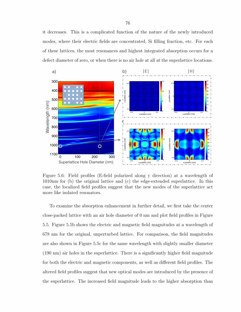
76
it decreases. This is a complicated function of the nature of the newly introduced
modes, where their electric fields are concentrated, Si filling fraction, etc. For each
of these lattices, the most resonances and highest integrated absorption occurs for a
defect diameter of zero, or when there is no air hole at all at the superlattice locations.
Defect Diameter (nm)
Wav
elen
gth
(nm
)
0 100 200 300
300
400
500
600
700
800
900
1000
1100
0.1
0.2
0.3
0.4
0.5
0.6
0.7
0.8
0.9
Perfect'La*ce'(678nm)'
|E|' |H|'
Defect Diameter (nm)
Wav
elen
gth
(nm
)
0 100 200 300
300
400
500
600
700
800
900
1000
1100
Defect Diameter (nm)0 100 200 300
300
400
500
600
700
800
900
1000
1100
Defect Diameter0 100 200 300
300
400
500
600
700
800
900
1000
1100Defect Diameter (nm)
0 100 200 300
300
400
500
600
700
800
900
1000
1100
Center (close packed)! Center (extended)! Edge (extended)!Edge (close packed)!
Optimizing Defect Configuration (RCWA simulations of absorption)
perfect lattice!
x position (nm)
y po
sitio
n (n
m)
Edge Ext 0D 1014nm Htot
−0.5 0 0.5
−0.5
0
0.50
5
10
15
20
25
30
35
40
45
x position (nm)
y po
sitio
n (n
m)
Edge Ext 0D 1014nm Etot
−0.5 0 0.5
−0.5
0
0.50
5
10
15
x position (nm)
y po
sitio
n (n
m)
Edge Ext 232D 1014nm Etot
−0.5 0 0.5
−0.5
0
0.50
5
10
15
x position (nm)
y po
sitio
n (n
m)
Edge Ext 232D 1014nm Htot
−0.5 0 0.5
−0.5
0
0.50
5
10
15
20
25
30
35
40
45
a) b)
c'
Sublattice Hole Diameter (nm)!
Wav
elen
gth
(nm
)
Superlattice Hole Diameter (nm)
Figure 5.6: Field profiles (E-field polarized along y direction) at a wavelength of1010nm for (b) the original lattice and (c) the edge-extended superlattice. In thiscase, the localized field profiles suggest that the new modes of the superlattice actmore like isolated resonators.
To examine the absorption enhancement in further detail, we first take the center
close-packed lattice with an air hole diameter of 0 nm and plot field profiles in Figure
5.5. Figure 5.5b shows the electric and magnetic field magnitudes at a wavelength of
678 nm for the original, unperturbed lattice. For comparison, the field magnitudes
are also shown in Figure 5.5c for the same wavelength with slightly smaller diameter
(190 nm) air holes in the superlattice. There is a significantly higher field magnitude
for both the electric and magnetic components, as well as different field profiles. The
altered field profiles suggest that new optical modes are introduced by the presence of
the superlattice. The increased field magnitude leads to the higher absorption than

77
the case without the superlattice. Also worth nothing with these field profiles is the
fact that the new modes appear to be extended modes rather than isolated defect
resonances. This is likely as the locations of the new defect air holes are reasonably
close, and any mode that would exist inside one of these holes would couple with a
neighboring mode, forming a periodic set of coupled resonators analogous to the tight
binding description of bound states in solid-state physics.
Angle (degrees)
Wav
elen
gth
(nm
)
a290, d232 TM−TE Average
0 20 40 60 80
300
400
500
600
700
800
900
1000
1100
0.1
0.2
0.3
0.4
0.5
0.6
0.7
0.8
0.9
Angle (degrees)
Wav
elen
gth
(nm
)
a290, d232, x000 Enhancement Ratio
0 20 40 60 80
300
400
500
600
700
800
900
1000
1100
5
10
15
20
25
30
35
40a290, d232,x000 TM−TE Average
Angle (degrees)
Wav
elen
gth
(nm
)
0 20 40 60 80
300
400
500
600
700
800
900
1000
1100
0.1
0.2
0.3
0.4
0.5
0.6
0.7
0.8
0.9
a) b) c)
Wav
elen
gth
(nm
)
Wav
elen
gth
(nm
)
Wav
elen
gth
(nm
) Angle (degrees) Angle (degrees) Angle (degrees)
Figure 5.7: TE-TM averaged angular absorption spectra for (a) the original lattice,and (b) the center close-packed superlattice. (c) Absorption enhancement ratio ob-tained by dividing spectra (a) by spectra (b).
Next we examine field profiles from a lattice that has a larger separation between
superlattice points, the edge extended lattice. Figure 5.6 shows field profiles for
modes at a wavelength at 1010 nm with a superlattice air hole diameter of 0 nm and
for the original lattice. Again, it can be seen that the field magnitudes are much
higher for the case with the superlattice, leading to the higher absorption at this
wavelength. The field profiles are also very different for each case. Here, the fields for
the superlattice case are more isolated than for the center close-packed lattice, acting
more like weakly interacting resonators. This is because the superlattice positions
are separated by a larger distance and their resonant field profiles overlap less with
neighboring resonators.

78
In Figure 5.7 we compare the TM-TE averaged angular spectra for the original
lattice and the angular spectra for the center close-packed superlattice that has a
superlattice air hole diameter of 0 nm. Additional resonances introduced by the
superlattice are present at all angles contributing to increased absorption. The fact
that they strongly shift in frequency with angle suggests that the defects in this
case are coupled together as mentioned above, forming an in-plane coupled resonator
waveguide [44] with its own dispersion characteristics. We also plot the absorption
enhancement ratio for these two cases in Figure 5.7c, which gives a clear map of all
the new resonances introduced by the superlattice.
0 10 20 30 40 50 60 70 80 902
4
6
8
10
12
14
16Jsc − a290, d232, x000
Angle (degrees)
J (m
A /
cm2 )
Angle (degrees)
Abso
rbed
Cur
rent
(mA
/ cm
2 )
Figure 5.8: Integrated absorbed current for the center close-packed superlattice (solidline) and the original lattice (dashed line) as a function of incident angle, averagedover TE and TM modes and weighted by the AM 1.5 solar spectral current.
In addition to the new resonances introduced by the defects, incoupling to many
of the modes present in the simple periodic photonic crystal are altered in the super-
lattice, as can be seen by the enhanced absorption for the superlattice even for some
modes that were also present in the simple periodic photonic crystal. This altered
incoupling to the modes of the simple periodic crystal structure could be due to al-
tered reflectivity or through altered scattering due to the change in local dielectric
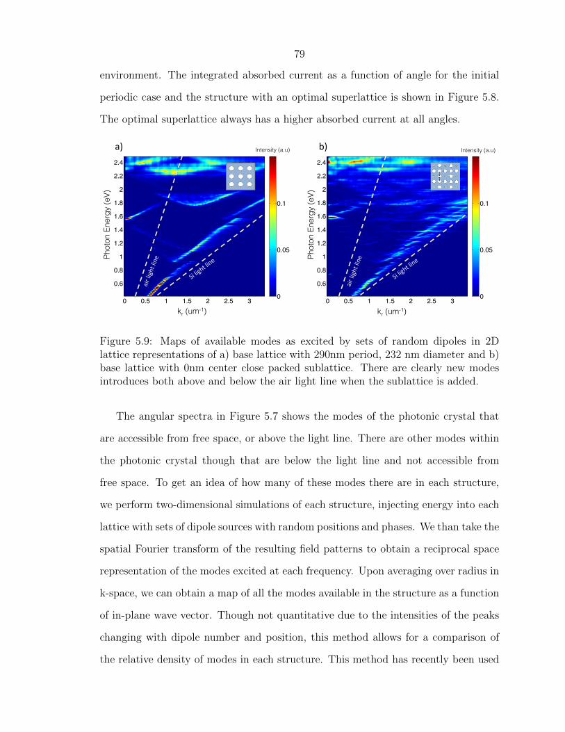
79
environment. The integrated absorbed current as a function of angle for the initial
periodic case and the structure with an optimal superlattice is shown in Figure 5.8.
The optimal superlattice always has a higher absorbed current at all angles.
a290d232 (5dipoles, 400freqs)
kr (um−1)
Phot
on E
nerg
y (e
V)
0 0.5 1 1.5 2 2.5 3
0.6
0.8
1
1.2
1.4
1.6
1.8
2
2.2
2.4
0
0.05
0.1
a290d232x000 (5Ds, 400freqs)
kr (um−1)Ph
oton
Ene
rgy
(eV)
0 0.5 1 1.5 2 2.5 3
0.6
0.8
1
1.2
1.4
1.6
1.8
2
2.2
2.4
0
0.05
0.1
a)# b)#
kr (um-1) kr (um-1)
Phot
on E
nerg
y (e
V)
Phot
on E
nerg
y (e
V)
Intensity (a.u) Intensity (a.u)
2D#dipole#k.vector#analysis:#a290d232#
Clearly#more#dense#modes#both#above#and#below#the#air#light#line#for#superlaAce.#Figure 5.9: Maps of available modes as excited by sets of random dipoles in 2D
lattice representations of a) base lattice with 290nm period, 232 nm diameter and b)base lattice with 0nm center close packed sublattice. There are clearly new modesintroduces both above and below the air light line when the sublattice is added.
The angular spectra in Figure 5.7 shows the modes of the photonic crystal that
are accessible from free space, or above the light line. There are other modes within
the photonic crystal though that are below the light line and not accessible from
free space. To get an idea of how many of these modes there are in each structure,
we perform two-dimensional simulations of each structure, injecting energy into each
lattice with sets of dipole sources with random positions and phases. We than take the
spatial Fourier transform of the resulting field patterns to obtain a reciprocal space
representation of the modes excited at each frequency. Upon averaging over radius in
k-space, we can obtain a map of all the modes available in the structure as a function
of in-plane wave vector. Though not quantitative due to the intensities of the peaks
changing with dipole number and position, this method allows for a comparison of
the relative density of modes in each structure. This method has recently been used
80
to investigate similar aperiodic structures [65]. Our results are shown in Figure 5.9.
It is clear that there are additional modes both above and below the air light line for
the superlattice case. Though not accessible for light incident on the photonic crystal
alone, these additional modes could be excited with the addition of a scattering layer
above or below the photonic crystal, as we will show below.
5.3 Superlattices In An Optimized Hexagonal Pho-
tonic Crystal
The addition of superlattices can be beneficial in many situations. To emphasize this,
we now test this concept on a different starting simple periodic lattice. We begin with
a hexagonal lattice of air holes in a 200 nm thick slab that has been optimized for
absorbed current with respect to lattice constant and air hole diameter. We then
introduce a rectangular superlattice on top of the original, forming what is known
as a Suzuki lattice [68]. In addition to this, we test one other case by extending the
rectangular superlattice into what we term the extended Suzuki lattice. Figure 5.10
shows the spectral absorption for these two cases as we vary the superlattice air hole
diameter.
Again shown for reference is the original lattice case indicated with a vertical
dotted white line. Similar to the square lattice case, increased absorption can be
seen on either side of the dotted line at certain wavelengths, corresponding to the
introduction of new resonances in the film when the superlattice is introduced. In
Figure 5.11, we again plot the integrated absorption weighted by the solar spectrum
and see that there is again always a superlattice case that outperforms the original
lattice. A difference in this case, however, is that the optimum superlattice air hole
diameters are not at 0 nm, instead they lie at slightly smaller diameters than the
original lattice. The overall enhancement over the original lattice is also less, due to
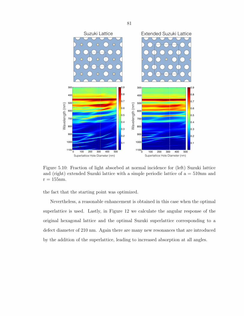
81
Suzuki Lattice a510d310
Sublattice Air Hole Diameter (nm)
Wav
elen
gth
(nm
)
0 100 200 300 400 500
300
400
500
600
700
800
900
1000
1100
0.1
0.2
0.3
0.4
0.5
0.6
0.7
0.8
0.9Extended Suzuki Lattice a510d310x210
Defect Diameter (nm)
Wav
elen
gth
(nm
)
0 100 200 300 400 500
300
400
500
600
700
800
900
1000
1100
0.1
0.2
0.3
0.4
0.5
0.6
0.7
0.8
0.9
Suzuki Lattice! Extended Suzuki Lattice!
Sublattice Hole Diameter (nm)! Sublattice Hole Diameter (nm)!
Wav
elen
gth
(nm
)
Wav
elen
gth
(nm
)
Superlattice Hole Diameter (nm) Superlattice Hole Diameter (nm)
Suzuki Lattice Extended Suzuki Lattice
Figure 5.10: Fraction of light absorbed at normal incidence for (left) Suzuki latticeand (right) extended Suzuki lattice with a simple periodic lattice of a = 510nm andr = 155nm.
the fact that the starting point was optimized.
Nevertheless, a reasonable enhancement is obtained in this case when the optimal
superlattice is used. Lastly, in Figure 12 we calculate the angular response of the
original hexagonal lattice and the optimal Suzuki superlattice corresponding to a
defect diameter of 210 nm. Again there are many new resonances that are introduced
by the addition of the superlattice, leading to increased absorption at all angles.
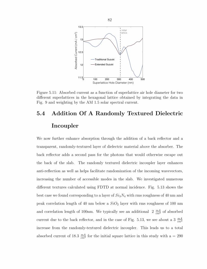
82
0 100 200 300 400 50011.5
12
12.5
13
13.5
Superlattice Hole Diameter (nm)
Jsc
(mA/
cm2)
Traditional Suzuki
Extended Suzuki
Sublattice Hole Diameter (nm)!Superlattice Hole Diameter (nm)
Abso
rbed
Cur
rent
(mA
/ cm
2 )
initial lattice
Figure 5.11: Absorbed current as a function of superlattice air hole diameter for twodifferent superlattices in the hexagonal lattice obtained by integrating the data inFig. 9 and weighting by the AM 1.5 solar spectral current.
5.4 Addition Of A Randomly Textured Dielectric
Incoupler
We now further enhance absorption through the addition of a back reflector and a
transparent, randomly-textured layer of dielectric material above the absorber. The
back reflector adds a second pass for the photons that would otherwise escape out
the back of the slab. The randomly textured dielectric incoupler layer enhances
anti-reflection as well as helps facilitate randomization of the incoming wavevectors,
increasing the number of accessible modes in the slab. We investigated numerous
different textures calculated using FDTD at normal incidence. Fig. 5.13 shows the
best case we found corresponding to a layer of Si3N4 with rms roughness of 40 nm and
peak correlation length of 40 nm below a SiO2 layer with rms roughness of 100 nm
and correlation length of 100nm. We typically see an additional 2 mAcm2 of absorbed
current due to the back reflector, and in the case of Fig. 5.13, we see about a 3 mAcm2
increase from the randomly-textured dielectric incoupler. This leads us to a total
absorbed current of 18.3 mAcm2 for the initial square lattice in this study with a = 290

83
a510d310x210Suzuki Hexagonal, TMTE Ave
Angle (degrees)
Wav
elen
gth
(nm
)
0 20 40 60 80
300
400
500
600
700
800
900
1000
1100 0
0.1
0.2
0.3
0.4
0.5
0.6
0.7
0.8Enhancement Ratio for Hex d310a510x290
Angle (degrees)
Wav
elen
gth
(nm
)
0 100 200 300 400 500
300
400
500
600
700
800
900
1000
1100
5
10
15
20
25a510d310x210Suzuki Hexagonal, TMTE Ave
Angle (degrees)
Wav
elen
gth
(nm
)
0 20 40 60 80
300
400
500
600
700
800
900
1000
1100 0
0.1
0.2
0.3
0.4
0.5
0.6
0.7
0.8
Wav
elen
gth
(nm
)
Angle (degrees)
Wav
elen
gth
(nm
)
Angle (degrees)
Wav
elen
gth
(nm
)
Angle (degrees)
a) b) c)
Figure 5.12: TE-TM averaged angular absorption spectra for (a) the original hexag-onal lattice, (b) the optimal superlattice, and (c) the enhancement ratio.
nm and d = 232 nm. When this same texturing is placed on the optimal hexagonal
superlattice case (a = 510 nm, d = 310 nm, dsuperlattice = 210 nm) we achieve a
absorbed current of 19.5 mAcm2 .
Figure 5.13: Schematic of a planar slab with roughened texturing (left) and thehighest-performing structure (right), wherein a photonic crystal superlattice is inte-grated with a randomly textured dielectric incoupler.
Additionally, when we start with a different square lattice with optimized pe-
riod and air hole diameter (a = 550 nm, d = 350 nm) and add an optimized edge
close-packed superlattice (dsuperlattice = 300 nm), as well as a randomly-textured

84
dielectric incoupler, we observe the highest absorbed current of this study at 20.7
mAcm2 . This is still less than the ergodic limit at 200 nm total thickness which is 31
mAcm2 . If we instead use the equivalent thickness of our structure, which is 144 nm, the
optimal structure is closer but still below the ergodic limit at this thickness of 29mAcm2 .
While a different structure may be necessary to reach or exceed the ergodic limit, the
absorbed current of 20.7 mAcm2 is still more than 2 times larger than that of a planar
Si slab with the same roughened texturing at 9.96 mAcm2 , as shown in Figure 5.13. We
have also confirmed that each of the optimized superlattice structures have higher
absorbed currents than the same randomly-textured dielectric incoupler applied to
each of their respective starting lattices. These higher currents are achieved with the
same incoupler due to the greater number of modes in the optimized superlattice than
both the planar slab and the starting lattice.
5.5 Thicker Absorber Layers
The previous calculations were all done for 200 nm thick Si slabs mainly to illustrate
the effects of different light trapping strategies. For thin layer Si cells to be compet-
itive with commercial Si photovoltaic efficiencies, slightly thicker active regions and
higher currents are necessary. To show that our approach can be extended to thicker
absorbing regions, we simulated superlattice photonic crystal layers with randomly-
textured dielectric incouplers with Si thicknesses of 1 to 4 microns, which can result
in absorbed currents between 30 and 40 mAcm2 . For example, our 2 um thick cell has
∼ 34 mAcm2 , comparable to other results in the literature [69] with similar thicknesses.
It is also worth noting that we do not use equivalent thickness as a metric as it can
complicate comparison of different patterns. These currents are not only approaching
the ergodic ray optic light trapping limit for these thicknesses, but also show that our
designs may be implemented to create thin film cells that are competitive in efficiency
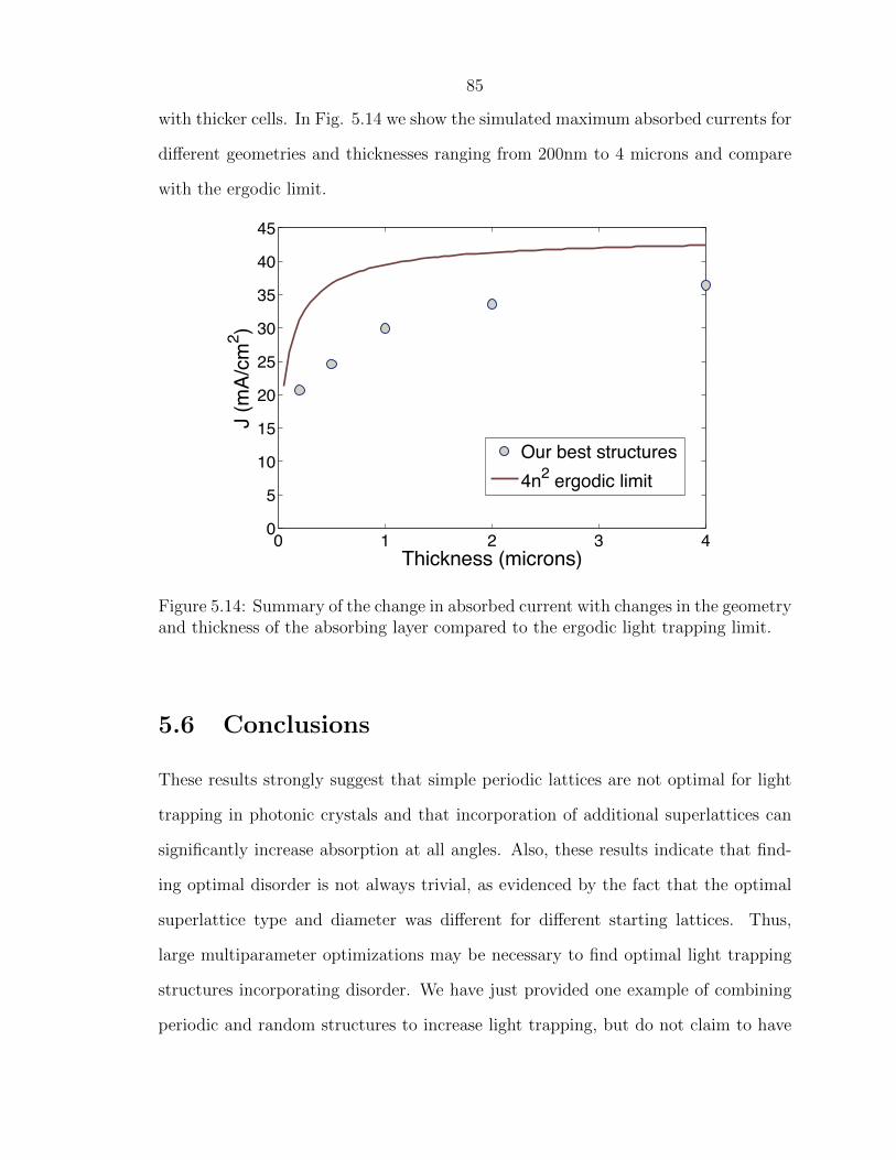
85
with thicker cells. In Fig. 5.14 we show the simulated maximum absorbed currents for
different geometries and thicknesses ranging from 200nm to 4 microns and compare
with the ergodic limit.
Thickness (um)
Abso
rbed
Cur
rent
(mA
/ cm
2 )
0 1 2 3 40
5
10
15
20
25
30
35
40
45
Thickness (microns)
J (m
A/cm
2 )
Our best structures4n2 ergodic limit
Figure 5.14: Summary of the change in absorbed current with changes in the geometryand thickness of the absorbing layer compared to the ergodic light trapping limit.
5.6 Conclusions
These results strongly suggest that simple periodic lattices are not optimal for light
trapping in photonic crystals and that incorporation of additional superlattices can
significantly increase absorption at all angles. Also, these results indicate that find-
ing optimal disorder is not always trivial, as evidenced by the fact that the optimal
superlattice type and diameter was different for different starting lattices. Thus,
large multiparameter optimizations may be necessary to find optimal light trapping
structures incorporating disorder. We have just provided one example of combining
periodic and random structures to increase light trapping, but do not claim to have

86
found an absolute best combination. Much more work is needed to fully explore the
other regions of the periodic to random continuum depicted schematically in Fig. 5.1.
Two obvious extensions of the superlattice structures we have studied would be to
introduce defects at non-periodic sites in a photonic crystal lattice and to use a poly-
disperse size distribution of defects. These scenarios are much more computationally
demanding and thus were not explored in this work, but will be the subject of future
work. We have also shown that the combination of superlattice photonic crystals with
randomly-textured dielectric incouplers significantly increases absorption. This is due
to the fact that rough surfaces randomize incoming photons, lifting the constraint of
selective mode occupation that occurs with periodic structures. These findings lend
support to the idea that for most light trapping applications, a combination of peri-
odic and random texturing may be optimal.

87
Chapter 6
Light Trapping In Thin Film GaAs
6.1 Introduction
GaAs is an ideal material for photovoltaic energy conversion. It has a direct bandgap
well matched to the AM1.5G spectrum [54], can be epitaxially grown in high single
crystal quality, and can be passivated with other III-V materials in the same epitaxial
growth process. Traditionally, GaAs solar cells have been grown on substrate wafers,
with the active device roughly index matched to the thick, inactive substrate mate-
rial (∼hundreds of microns). This makes light trapping difficult as nearly all photons
incident on the device only get a single pass through the material. If they are not
absorbed on the first pass, they enter the substrate where they are parasitically ab-
sorbed. Adding a back reflector or scattering surface to the wafer would be useless,
as nearly all of the photons would be absorbed before reaching it. As a result, the
active regions of high efficiency GaAs cells have traditionally been several microns
thick.
Recently, GaAs cells have had renewed interest due to the process of epitaxial
liftoff (ELO) [70, 71] in which the active device region can be removed from the
substrate and placed on a reflective surface. This has allowed GaAs to achieve the
world record single junction efficiency record [15], which has been steadily increasing
for the last several years due to the efforts of the solar startup Alta Devices. One
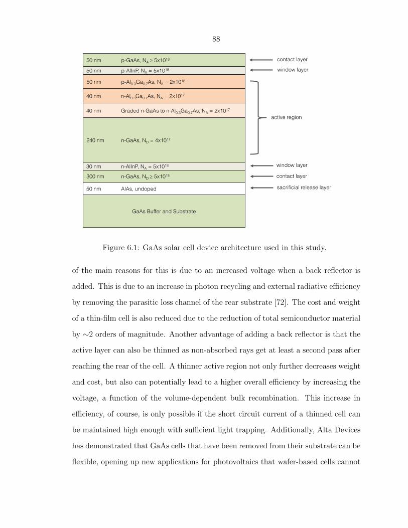
88
240 nm n-GaAs, ND = 4x10¹⁷
50 nm p-Al0.3Ga0.7As, NA = 2x10¹⁸
50 nm p-AlInP, NA = 5x10¹⁸
50 nm p-GaAs, NA ≥ 5x10¹⁸
300 nm n-GaAs, ND ≥ 5x10¹⁸
40 nm n-Al0.3Ga0.7As, NA = 2x10¹⁷
40 nm Graded n-GaAs to n-Al0.3Ga0.7As, NA = 2x10¹⁷
30 nm n-AlInP, NA = 5x10¹⁸
50 nm AlAs, undoped
GaAs Buffer and Substrate
contact layer
window layer
active region
contact layer
window layer
sacrificial release layer
Figure 6.1: GaAs solar cell device architecture used in this study.
of the main reasons for this is due to an increased voltage when a back reflector is
added. This is due to an increase in photon recycling and external radiative efficiency
by removing the parasitic loss channel of the rear substrate [72]. The cost and weight
of a thin-film cell is also reduced due to the reduction of total semiconductor material
by ∼2 orders of magnitude. Another advantage of adding a back reflector is that the
active layer can also be thinned as non-absorbed rays get at least a second pass after
reaching the rear of the cell. A thinner active region not only further decreases weight
and cost, but also can potentially lead to a higher overall efficiency by increasing the
voltage, a function of the volume-dependent bulk recombination. This increase in
efficiency, of course, is only possible if the short circuit current of a thinned cell can
be maintained high enough with sufficient light trapping. Additionally, Alta Devices
has demonstrated that GaAs cells that have been removed from their substrate can be
flexible, opening up new applications for photovoltaics that wafer-based cells cannot

89
be used for.
Here, we extend this concept further to even thinner active regions well below a
micron. At these thicknesses, the cell can be considered “optically thin” (i.e. thin
enough that even with perfect anti-reflection, a planar cell will not absorb enough
photons to reach a reasonable efficiency). At these thicknesses, advanced light trap-
ping schemes are needed. We design and fabricate ultrathin GaAs solar cells of
∼300nm and remove the devices from their native substrates using the process of
epitaxial liftoff. We further process them into functioning devices by mesa etching
and electrical contacting.
Devices After Processing
1.5 cm
2 mm
Single mesa
a) c)
V
J (m
A / c
m2 )
b)
Figure 6.2: a) Image of lifted-off sample containing numerous GaAs devices after fullprocessing, b) Image of single GaAs device after processing. c) Typical J-V curve ofa cell after processing, before AR or nanoparticle deposition.
We then numerically examine ways of enhancing the absorption of a GaAs thin-
film solar cell with various periodic nanopatterns of TiO2 cylinders above the active
region of the device. We examine the expected angular behavior of the cell and show
that with the appropriate patterning, a periodically textured cell can outperform a

90
cell with an optimized anti-reflection coating at all incident angles. We then identify
additional sources of photocurrent loss and identify ways of further increasing the
solar absorption with additional device processing.
We then develop and implement a process for patterning thin GaAs solar cells with
TiO2 nanocylinders using the process nano-imprint lithography. We demonstrate this
as a viable route to ultra-thin solar cells with significant enhanced absorption from a
scalable, low-loss light trapping scheme.
6.2 Epitaxial Liftoff of Ultra-thin Film GaAs
GaAs heterojunction solar cells were grown via metal organic chemical vapor depo-
sition (MOCVD) on a GaAs substrate wafer with an intermediate AlAs release layer
at an outside chemical foundry, IQE. The full heterostructure is shown in Fig. 1.
The AlAs layer preferentially etches at a rate 107 times faster than GaAs [71] and
significantly faster than the other layers in the device in a hydrofluoric acid (HF)
solution.
IQE12-3 IQE12-1
V V
J (m
A / c
m2 )
J (m
A / c
m2 )
Jsc Ave = 12.60 mA/cm2 ± 0.35 mA/cm2
Voc Ave = 1.025 V ± 0.006 V
Jsc Ave = 12.98 mA/cm2 ± 0.41 mA/cm2
Voc Ave = 1.019 V ± 0.026 V
Figure 6.3: Sample to sample and cell to cell variation in thin-film GaAs J-V curvesmade via epitaxial liftoff. Each plot is a different 1.5 cm x 1.5 cm processed sample.Each trace in a different, mesa-isolated cell.

91
The wafers were diced into 1.5x1.5 cm2 squares before processing. The surface
was cleaned by blowing with a supercritical CO2 sno-gun, followed by soniciation in
acetone and isopropyl alcohol. They were then dipped in a hydrochloric acid solution
for 30s, and dried with nitrogen. A thin 3 nm Ni layer was evaporated on the device
side of the sample with ebeam evaporation at ∼1x10⁻⁷ Torr, followed by 200 nm of
thermally evaporated Cu. The samples were then immersed in a Cu electroplating
solution and ∼100-200 um of Cu was electroplated on the thermally evaporated metal.
Following this, excess electroplated Cu on the edges of the sample was removed with
a razor blade, and the samples were attached to a flexible plastic Kapton handle with
bonding wax. The samples were then etched in 10% hydrofluoric acid overnight to
release the device from the substrate. Following ELO, 2x2 mm devices were isolated
by mesa etching. Finally, Ni/Cu top contacts were deposited via ebeam and thermal
evaporation as before.
IQE GaAs Cell AR Coating Optimization
TiO2 Thickness (nm)
SiO
2 Th
ickne
ss
0 50 100 150 200
0
50
100
150
20015
15.5
16
16.5
17
17.5
18
18.5
19
SiO
2 Thi
ckne
ss (n
m)
TiO2 Thickness (nm)
240nm GaAs/80nm AlGaAs
Cu
30nm AlInP window-layer
50nm AlInP window-layer
t SiO2 t TiO2
50nm GaAs Contact
Absorbed Current (mA/cm2) a) b)
Figure 6.4: a) Layered structure used in the electromagnnetic simulations. b) Bilayeranti-reflection coating optimization for the GaAs solar cell used in this study.
Current-voltage curves were taken for each of the mesa-isolated cells on each
sample. Figure 3 shows current density-voltage curves for multiple cells on 2 different

92
1.5x1.5 cm ELO samples. Each lifted off sample contains 21 different 2x2 mm mesa-
isolated cells. Cell to cell variation is small, but can be attributed to slight differences
in surface and edge texture, contact variation, and slight curvature variations of the
thin, non-rigid device/Cu handle.
Diameter (nm)
Pitc
h (n
m)
TiO2 Rod Optimization, 250nm H, conformal SiO2 (IQE GaAs cell, new AlInP)
150 200 250 300350
400
450
500
550
21.5
22
22.5
23
23.5
n-GaAs 240 nm
Graded n-AlGaAs 40 nm n-Al0.3Ga0.7As 40 nm p-Al0.3Ga0.7As 50 nm
p-AlInP 50 nm p-GaAs contact 50 nm
n-AlInP 30 nm
Ni 5 nm Cu 150nm
TiO2 SiO2
250nm H
D P
TiO2 Rod Optimization With IQE Cell
Absorbed Current (mA/cm2)
a) b)
Figure 6.5: a) Schematic of nanopattern and optimization parameters. b) Squarelattice TiO2 cylinder FDTD optimization.
6.3 Pattern Optimization and Electromagnetic Sim-
ulations
We perform full-field electromagnetic calculations to investigate the absorption of
the thin-film GaAs solar cell with and without various nanopatterning. Spectral ab-
sorption of the GaAs solar cell after ELO was calculated using the finite-difference
time domain (FDTD) method with a commercial software package, Lumerical. First,
optimal thicknesses for a bilayer anti-reflection coating made of TiO2 and SiO2 was
calculated via a 2 parameter thickness optimization. The figure of merit for this op-

93
timization was the AM1.5G weighted absorbed current. This was obtained by taking
the spectral absorption spectrum (i.e. fraction absorbed as a function of wavelength)
and multiplying it by the binned spectral current in the AM1.5G spectrum. Upon
integration over all wavelengths above the bandgap of GaAs, an absorbed current
density is obtained. This would be synonomous with the often used short circuit cur-
rent (Jsc) density if perfect electrical collection is assumed. The results of a bilayer
anti-reflection coating optimization is shown in Figure 4.
GaAs, IQE cell, planar, Optmized AR, TMTE
Angle (degrees)
Wav
elen
gth
(nm
)
0 20 40 60 80
300
400
500
600
700
800 0.1
0.2
0.3
0.4
0.5
0.6
0.7
0.8
0.9GaAs, a470d280h300 TiO2 Rods, conformal SiO2, TMTE
Angle (degrees)
Wav
elen
gth
(nm
)
0 20 40 60 80
300
400
500
600
700
800 0.1
0.2
0.3
0.4
0.5
0.6
0.7
0.8
0.9Abs. Abs.
Calculated Angular Spectra
Figure 6.6: RCWA simulations of angular response of a) GaAs cell with planar opti-mized anti-reflection coating and b) optimized TiO2 cylinder nanopattern.
FDTD was then used to determine the optimal nanopattern that maximizes the
AM1.5G spectrally integrated absorbed current. Numerous optimizations were per-
formed for different lattices, different cylinder heights, different back reflectors, etc.
An example of an optimization for a hexagonal lattice of TiO2 rods coated with a
conformal 90nm SiO2 layer on an Ni/Cu back reflector is shown in Figure 5. It can
be seen that the absorbed current is significantly higher than what was optained with
the optimized bilayer anti-reflection coating from Figure 4.
To examine the angular behavior of the nanopattern, calculations were performed
with rigorous coupled wave analysis (RCWA) for both TM and TE polarizations over

94
an angular range of 0-88 degrees. The results are shown in Figure 6. Also shown for
comparison is the angular behavior of the cell with the optimized planar anti-reflection
coating.
0 20 40 60 800
5
10
15
20
25
GaAs, IQE Cell
Angle (degrees)
Abso
rbed
Cur
rent
(mA/
cm2 )
TiO2 Rods (a470d280h300)Planar, optimal 2−layer AR
240nm GaAs/80 AlGaAs
Ag
30 AlInP window-layer
50 AlInP window-layer
80 nm SiO2 25 nm TiO2
240nm GaAs/80 AlGaAs
Ag
SiO2 ARC
TiO2 30 AlInP window-layer
50 AlInP window-layer
H = 300 nm
D = 280 nm P = 470 nm
Calculated Angular Spectra (integrated)
50nm GaAs Contact
50nm GaAs Contact
Patterned
Planar
Figure 6.7: AM1.5G spectrally integrated absorbed current for the planar anti-reflection coated cell and the TiO2 nanopatterned cell.
There is clearly increased absorption with the nanopattern, paricularily in the
long wavelength range near the GaAs bandgap. For a more quantitative comparison,
the AM1.5G spectrally integrated absorbed current is calculted for each angle and
plotted in Figure 7.
The enhanced absorption occurs due to numerous photonic resonances introduced
by the periodic nanopattern. Some of these resonances change their spectral position
as a function of angle, while others are relatively insensitive to the incident angle. To
further examine the nature of these resonances, we plot the electric field intensity as
a function of position at different wavelengths and angles in Figure 8.
At the points labeled “a” and “b” in Figure 8, the electric field shows a localized
field within the TiO2 cylinder above a Fabry-Perot type resonance in the planar solar
cell. This same field pattern occurs at incident angles of both 40 and 60 degrees along

95
GaAs, a470d280h300 TiO2 Rods, conformal SiO2, TMTE
Angle (degrees)
Wav
elen
gth
(nm
)
0 20 40 60 80
300
400
500
600
700
800 0.1
0.2
0.3
0.4
0.5
0.6
0.7
0.8
0.9
SqP470D280t60TM848nm
−200 −100 0 100 200
−600
−400
−200
0
200
400
0
0.5
1
1.5
2
2.560o 848 nm (TM) SqP470D280t40TM860nm
−200 −100 0 100 200
−600
−400
−200
0
200
400
0
0.5
1
1.5
2
2.5
3
3.5
4
4.5
40o 860 nm (TM)
40o 820 nm (TM) SqP470D280t60TM810nm
−200 −100 0 100 200
−600
−400
−200
0
200
400
0
0.5
1
1.560o 810 nm (TM)
GaAs, a470d280h300 TiO2 Rods, conformal SiO2, TMTE
Angle (degrees)
Wav
elen
gth
(nm
)
0 20 40 60 80
300
400
500
600
700
800 0.1
0.2
0.3
0.4
0.5
0.6
0.7
0.8
0.9
0
1
Normalized |E|2
GaAs, a470d280h300 TiO2 Rods, conformal SiO2, TMTE
Angle (degrees)W
avel
engt
h (n
m)
0 20 40 60 80
300
400
500
600
700
800 0.1
0.2
0.3
0.4
0.5
0.6
0.7
0.8
0.9
Abs. SqP470D280t40TM820nm
−200 −100 0 100 200
−600
−400
−200
0
200
400
0
0.5
1
1.5
2
2.5
a b
c d
a b
c d
Square
Figure 6.8: Electric field intensities for several resonant modes observed in the angularabsorption spectrum.
the same resonance line in the angular absorption spectrum. Since these resonances
are localized and not propagating in-plane, they are relatively insensitive to incident
angle and can be considered non-dispersive. A different type of mode is seen at points
“c” and “d” in Figure 8. These field profiles reveal a periodic, propagating mode in
the solar cell region. These types of modes have their own dispersion and change
spectral position with incident angle as the incident in-plane wavevector is changed.
Since they are not present in the planar absorption spectrum, the periodic array above
the solar cell must be incoupling incident light into these normally ”trapped” modes
of the high index solar cell.
While the enhanced absorption introduced by the TiO2 nanopattern is significant,
the integrated absorbed current is still well below the theoretical value of ∼31 mAcm2 .
To examine where the remaining optical losses are, we calculate the absorption in
each of the layers of the structure and plot it in Figure 9.
A significant amount of absorption in the blue region of the spectrum occurs in
the top AlInP window layer. This is difficult to avoid without thinning this layer or
using a different material with lower absorption coefficient. In fact, even the current

96
300 400 500 600 700 8000
0.2
0.4
0.6
0.8
1GaAs IQE cell, a470d280h300, CuBR
Wavelength (nm)
Perc
ent A
bsor
bed
Cu AbsorptionGaAs bulk absorptionAlInP Bottom AbsorptionAlInP Top AbsorptionGaAs Back Contact AbsorptionReflection
Quantification Of Losses In Optimized TiO2 Rod Cell
Figure 6.9: Quantification of losses in each layer of the GaAs solar cell structure.
world record GaAs solar cell shows similar losses in the blue region of the spectrum
in the external quantum efficiency (EQE) curve [15]. Additional significant losses
occur in the rear 50nm highly doped GaAs contact layer. This layer is present solely
to achieve ohmic electrical contact between the device and rear metal. For III-V
materials with high conductivity and low sheet resistance like the ones used here,
electrical contact does not need to be made conformally over the entire planar area.
Significant portions of the contact layer could be removed and the device could be
contacted selectively as is done on the top surface of the device. This would result in
less interaction of the incident light with the lossy rear contact layer, resulting in less
parasitic absorption and potentially higher usefully absorbed current. Additionally,
if a low refractive index dielectric spacer is placed between the device and rear metal
reflector, reflection can occur at this interface and reduce interaction and loss at the
rear metal surface.
To quantify how much of an improvement is achieveable, we re-optimize a hexago-
nal periodic pattern of TiO2 cylinders on a device without a rear GaAs back reflector

97
Angle (degrees)
Wav
elen
gth
(nm
)
hex P540D260420SiO2noRearGaAs
0 20 40 60 80
300
400
500
600
700
800
0
0.2
0.4
0.6
0.8
1
Angle (degrees)
Wav
elen
gth
(nm
)
planar420SiO2noRearGaAs
0 20 40 60 80
300
400
500
600
700
800
0
0.2
0.4
0.6
0.8
1Abs. Abs.
Figure 6.10: Angular spectra of the GaAs solar cell with the rear contact removedwith and without addition of an optmized nanopattern.
and with an optimized dielectric spacer of refractive index 1.5. The angular spectra
of this structure compared with a similar structure without the TiO2 patterning is
shown in Figure 10.
Again, we see significant absorption enhancement in the long wavelength region
of the spectrum due to new modes being excited by the periodic nanopattern. To
compare all of the structures we have examined, we plot the integrated absorbed
current over all angles in Figure 11.
A significant increase in absorbed current is seen for both cases without a GaAs
rear contact layer. The highest absorbed current at all angles is achieved with an op-
timized TiO2 nanopattern on a cell without a rear GaAs contact layer and a dielectric
spacer between the device and rear reflector.
In reality, the entire GaAs contact layer cannot be removed to allow for selective
contact to the device. Because of this, the actual reduction in parasitic absorption
would be slightly less than calculated in these simulations. Since the dimensions of
typical contact stripes are much larger than the wavelength, the expected reduction
in parasitic absorption could be approximated using the fill fraction of removed GaAs
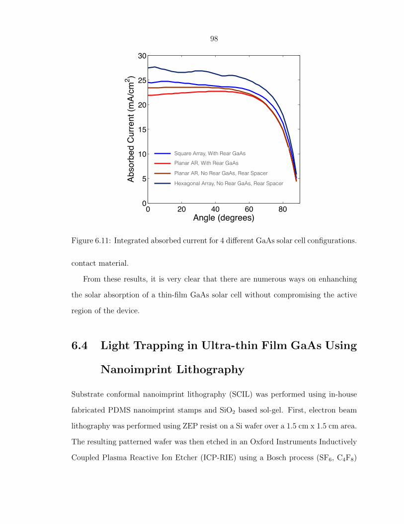
98
0 20 40 60 800
5
10
15
20
25
30GaAs, IQE Cell
Angle (degrees)
Abso
rbed
Cur
rent
(mA/
cm2 )
TiO2 Sq Rods (a470d280h300)
Planar, optimal 2−layer AR
Planar, 420SiO2, no Rear GaAs1
Hex Rods (a549d269h300, 420SiO2, noRGaAs)
Square Array, With Rear GaAs
Planar AR, With Rear GaAs
Planar AR, No Rear GaAs, Rear Spacer
Hexagonal Array, No Rear GaAs, Rear Spacer
Figure 6.11: Integrated absorbed current for 4 different GaAs solar cell configurations.
contact material.
From these results, it is very clear that there are numerous ways on enhanching
the solar absorption of a thin-film GaAs solar cell without compromising the active
region of the device.
6.4 Light Trapping in Ultra-thin Film GaAs Using
Nanoimprint Lithography
Substrate conformal nanoimprint lithography (SCIL) was performed using in-house
fabricated PDMS nanoimprint stamps and SiO2 based sol-gel. First, electron beam
lithography was performed using ZEP resist on a Si wafer over a 1.5 cm x 1.5 cm area.
The resulting patterned wafer was then etched in an Oxford Instruments Inductively
Coupled Plasma Reactive Ion Etcher (ICP-RIE) using a Bosch process (SF6, C4F8)
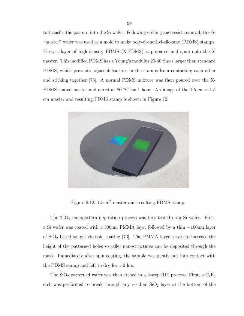
99
to transfer the pattern into the Si wafer. Following etching and resist removal, this Si
“master” wafer was used as a mold to make poly-di-methyl-siloxane (PDMS) stamps.
First, a layer of high-density PDMS (X-PDMS) is prepared and spun onto the Si
master. This modified PDMS has a Young’s modulus 20-40 times larger than standard
PDMS, which prevents adjacent features in the stamps from contacting each other
and sticking together [73]. A normal PDMS mixture was then poured over the X-
PDMS coated master and cured at 80 oC for 1 hour. An image of the 1.5 cm x 1.5
cm master and resulting PDMS stamp is shown in Figure 12.
Figure
Figure 6.12: 1.5cm2 master and resulting PDMS stamp.
The TiO2 nanopattern deposition process was first tested on a Si wafer. First,
a Si wafer was coated with a 300nm PMMA layer followed by a thin ∼100nm layer
of SiO2 based sol-gel via spin coating [73]. The PMMA layer serves to increase the
height of the patterned holes so taller nanostructures can be deposited through the
mask. Immediately after spin coating, the sample was gently put into contact with
the PDMS stamp and left to dry for 1-2 hrs.
The SiO2 patterned wafer was then etched in a 2-step RIE process. First, a C4F8
etch was performed to break through any residual SiO2 layer at the bottom of the

100
imprinted holes. Then, an O2 etch was performed to etch through the PMMA layer
beneath the SiO2.
Following etching, TiO2 was deposited via ebeam evaporation in an O2 environ-
ment at 1x10⁻⁵ Torr. The PMMA and SiO2 layers were then removed in acetone with
sonication. Figure 13 shows an optical image of the resulting TiO2 nanopattern on
the Si wafer. Most of the 1 cm x 1 cm area was uniformly covered in the nanopattern
as shown in the image. Scanning electron microscope (SEM) images of the same
pattern are shown in Figure 14.
TiO2 Deposition Through 1 cm2 Nanoimprinted Mask on Si
10 um
Figure 6.13: Optical image of a hexagonal pattern of TiO2 nanoparticles on Si witha period of 540 nm and diameter of 260 nm.
Before patterning the GaAs solar cells, they were conformally coated in a 25nm
TiO2 layer before imprinting. This thin TiO2 both acts as a bottom anti-reflection
layer and provides protection for the underlying GaAs during subsequent reactive
ion etching. The sample was then coated with a 300nm PMMA layer followed by a
thin ∼100nm layer of SiO2 based sol-gel via spin coating [73]. Immediately after spin
coating, the sample was gently put into contact with the PDMS stamp and left to

101
TiO2 Deposition Through 1 cm2 Nanoimprinted Mask on Si
1 um
2 um
0o tilt
70o tilt
Figure 6.14: SEM images of a hexagonal pattern of TiO2 nanoparticles on Si with aperiod of 540 nm and diameter of 260 nm.
dry for 1-2 hrs.
The SiO2 patterned GaAs solar cells were then etched in a 2-step RIE process. A
C4F8 etch was performed to break through any residual SiO2 layer at the bottom of
the imprinted holes. Then, an O2 etch was performed to etch through the PMMA
layer beneath the SiO2.
Following etching, TiO2 was deposited via ebeam evaporation in an O2 environ-
ment at 1x10⁻⁵ Torr. The PMMA and SiO2 layers were then removed in acetone and
sonication. Lastly, a 90nm SiO2 layer was deposited via ebeam evaporation to com-
plete the patterning. This SiO2 layer serves as a top anti-reflection layer. In parallel
with this patterned sample, a GaAs sample was prepared with a planar anti-reflection
coating with the same material thicknesses (25nm TiO2, 90nm SiO2). An image of
the final planar and nanopatterned GaAs solar cells are shown in Figure 15.
A 1.5 cm x 1.5 cm square sample was stamped with a 1 cm x 1 cm square stamp.
After full processing, this resulted in some devices on the sample having the nanopat-
tern and some devices having a 2-layer anti-reflection coating. This allows for com-
parison of cells from the same lift-off that were exposed to the exact same processing
conditions throughout fabrication. To ensure a fair comparison, many cells from

102
Figure 6.15: GaAs solar cells after TiO2 nanopatterning and SiO2 deposition.
the sample are not included in these results that were visably different from each
other. Reasons for the differences in cells despite the same processing conditions are
non-uniform contact liftoff, non-uniform PMMA/sol-gel liftoff, misaligned stamping,
visible cell damage, etc.
Current-density voltage curves for several cells on a single sample are shown in
Figure 16. Only 2 cells on this sample had uniform nanopattern coverage and were
free from other damage. Their average photocurrent was measured to be about 1 mAcm2
higher than cells on the same sample with only a 2-layer anti-reflection coating. The
total energy conversion efficiency of these devices is about ∼10-12%.
Because we have observed variation in Jsc of up to 1 mAcm2 as shown in Figure 3,
it is difficult to make a strong conclusion about these current density-voltage curves
until more samples have been tested and compared.
To further characterize the cells, external quantum efficiency measurements were
made on single cells that were half patterned and half coated with an anti-reflection
coating. This was achieved by aligning the edge of the nanoimprint stamp with the
center of a 2 mm x 2 mm cell. The cells were illuminated with a focused incident beam

103
GaAs, a470d280h300 TiO2 Rods, conformal SiO2, TMTE
Angle (degrees)
Wav
elen
gth
(nm
)
0 20 40 60 80
300
400
500
600
700
800 0.1
0.2
0.3
0.4
0.5
0.6
0.7
0.8
0.9Square
Voltage (V)
J (m
A / c
m2 )
Pattern Planar
Figure 6.16: Current density-voltage curves for cells with and without a TiO2
nanoparticle coating.
with a spot size ∼10 microns in diameter, allowing for measurements of each area of
the cell individually. Figure 17 shows external quantum efficiency measurements of
each of these areas on 2 different cells.
400 500 600 700 800 9000
0.2
0.4
0.6
0.8
1
Wavelength (nm)
Exte
rnal
Qua
ntum
Effi
cien
cy
cell 17, NP1cell 17, NP2cell 17, AR1cell 17, AR2
400 500 600 700 800 9000
0.2
0.4
0.6
0.8
1
Wavelength (nm)
Exte
rnal
Qua
ntum
Effi
cien
cy
cell 8, NP1
cell 8, AR1
19.64 mA/cm2
19.67 mA/cm2 19.33 mA/cm2
19.44 mA/cm2
19.23 mA/cm2
18.87 mA/cm2
Nanopattern, Spot 1 Nanopattern, Spot 2 Planar AR, Spot 1 Planar AR, Spot 2
Nanopattern
Planar AR
Figure 6.17: External quantum efficiency measurements of different positions of singlecells with and without nanopatterning.
These plots show that some regions of the spectrum are absorbed more efficently
with the nanopattern and some are better absorbed with the anti-reflection coating.
Also shown in Figure 17 are calculations of short-circuit current obtained by weighting

104
the EQE spectra with the spectral current in the AM1.5 spectrum and integrating
over all wavelengths. It can be seen that there is a slight (∼0.2-0.4 mAcm2 ) increase in
Jsc for the nanopatterned areas compared to the areas coated with an anti-reflection
coating. This result is qualitatively but not quantitatively the same as obtained from
J-V measurements.
The discrepancy in the values for short-circuit current obtained from the J-V
curves and EQE measurements could be due to several factors including shadow loss
(∼2 mAcm2 ), inhomogeneties in surface quality, calibration, etc.
IQE
EQE NP1 cell 17
Incident Angle (degrees)
Wav
elen
gth
(nm
)
0 20 40 60
400
500
600
700
800
900
0.1
0.2
0.3
0.4
0.5
0.6
0.7
0.8
0.9EQE Planar AR cell 17
Incident Angle (degrees)
Wav
elen
gth
(nm
)
0 20 40 60
400
500
600
700
800
900
0.1
0.2
0.3
0.4
0.5
0.6
0.7
0.8
0.9EQE EQE
Figure 6.18: Angle-dependent external quantum efficiency measurements of differentpositions of single cells with and without nanopatterning.
We also measure the angle-dependent EQE for different areas of a single GaAs
solar cell and plot the results in Figure 18. There is slightly more absorption in the
red region of the spectrum for the area of the cell with the nanopattern for most
angles. The planar cell also has a relatively flat response as the angle is changed
while the nanopatterned cell is slighty more sensitive to incident angle. To determine
which cell operates better under AM1.5G conditions, the EQE is again weighted by
the solar spectrum and plotted in Figure 19.
The nanopatterned area performs better at angles close to normal while the AR

105
IQE
0 20 40 6017
17.5
18
18.5
19
19.5
20
20.5
21
Incident Angle (degrees)
J sc (m
A / c
m2 ) f
rom
EQ
E M
easu
rem
ents
ARNPs
Nanopattern
Planar AR
Figure 6.19: Short-circuit current as a funtion of angle as determined from EQEmeasurements for nanopatterned and AR coated areas of a single cell.
coated areas have higher short-circuit current at steeper incident angles.
While these results are promising, they are still far from what we beleive can be
achieved with TiO2 nanopatterning. Reasons for the inferior performance possibly
include non-optimal TiO2 refractive index, non-optimal SiO2 coating, non-uniform
cell quality, and non-uniform and non-optimal imprinting due to non-ideal flatness of
the GaAs solar cell samples. Many of these factors can easily be improved with further
study and refinement and we believe that absorption enhancements approaching those
observed in simulation will be achievable in the near future using the processing and
fabrication schemes we have developed.
106
Chapter 7
Summary And Outlook
The main subject of this thesis was to examine the possibilities and limits for ma-
nipulation of light in thin solar cells using nanophotonics. As state of the art solar
cells aim to further increase efficiency and decrease cost and weight, their thicknesses
will inevitably decrease as much as can be tolerated. As discussed in Chapter 1, the
ultimate solar cell is one that is as thin as possible while also absorbing as much light
from the sun as a thick cell. For these reasons, advanced light trapping schemes and
understanding the consequences of wavelength-scale features on device performance
will be increasingly more important for future solar cell technology. The idea and
concepts explored in this thesis open up many interesting avenues for future work,
some of which are explained in detail here.
7.1 Exceeding The Ergodic Limit In Si
In Chapter 3, we have shown how the LDOS can be manipulated to enhance light
absorption to levels beyond previously defined limits. In practice, this is easier to
achieve using absorbing materials that have relatively low refractive indices (∼1.5 -
2.5), such as the P3HT:PCBM absorber we explored in Chapter 3. To achieve light
trapping in higher index, more common solar cell materials like Si, more advanced
designs than those featured in this thesis will be required. The photonic crystal

107
designs explored in Chapter 5 are a good start. To convincingly demonstrate that
this approach can be used to exceed the light trapping limit in Si, a more refined
effort specifically aimed at designing photonic crystal structures to increase the LDOS
over a small bandwidth is needed. This could be done with focused design as was
done in Chapter 5, or by more computationally demanding approaches, such as using
the maximization of the LDOS as a figure of merit in an advanced electromagnetic
optimization [74].
a) b)
c) d)
Figure 7.1: a) [from Sapienza et al, 2010] [75] Formation of effective optical cavitieswithin a 1-dimensional photonic crystal waveguide clad with appropriately disorderedscatterers. b) [from Sapienza et al, 2010] [75] Spectrally resolved intensity plots as afunction of position within the waveguide. Light is localized at different wavelengthsalong different positions in the waveguide, forming a novel type of broadband opticalcavity. c) Potential 2D design that could be used to demonstrate Anderson local-ization for solar cell applications: Thin film of weakly absorbing material (i.e. Si ora polymer) clad with appropriately designed scattering particles on both sides. d)Potential 1D design: Si wire array filled with dense powder of appropriately designedscattering particles. Light will be localized in the 1-dimensional waveguide formedby the Si wire.
A fundamentally different way of trapping light that has potential to increase the
108
LDOS in high index materials is Anderson localization of photons [76], caused by
multiple scattering on a scale shorter than the wavelength. Under the appropriate
conditions, the electric field is scattered multiple times within a single optical cycle,
and the photon becomes strongly localized. Surprisingly, this method of light trap-
ping has not been explored much in the context of increasing absorption for solar
energy harvesting. When Anderson localization of light occurs, an effective optical
cavity is formed, in which the LDOS is increased [75], as shown in Figure 7.1. We
also saw in Chapter 3 that besides increasing the LDOS, the other important criterion
for achieving optimal light trapping is the full and equal population of the internal
modes of the structure, typically achieved with a random, scattering surface. Ander-
son localization is achieved in certain, special cases of disordered media, and is thus
inherently random in nature. Structures that exhibit Anderson localization of pho-
tons therefore may be able to achieve both of the criteria for optimal light trapping
(increased LDOS and ability to populate the internal modes) at the same time in a
single structure. Two examples of potential geometries to explore this idea are shown
in Figure 7.1.
7.2 Purcell Enhanced Photovoltaics
In Chapter 3, we explored how increases in the LDOS can be used to increase light
trapping. Manipulation of the LDOS could also potentially affect other processes and
quantities inside ultrathin solar cells besides absorption and Jsc, for example, the Voc.
In a photovoltaic device, at open circuit, no current is collected and the number of
recombination events inside the solar cell equals the number of excitation events. In
the ideal case, the solar cell will radiate the same number of photons back to the sun as
it absorbs. This, of course, means that the external luminescence quantum efficiency
(EQEL) is unity. If this occurs, the Voc will take on its theoretically maximum
109
value [13, 77, 78]. As soon as the luminescence quantum efficiency decreases, there is
an immediate penalty on the Voc as described by the equation [78]:
Voc = V maxoc +
kT
qln(EQEL) (7.1)
This penalty will severely limit the new theoretically maximum detailed balance
overall efficiency of the solar cell and is why materials with very high intrinsic lumines-
cence QEs like GaAs (QE ∼99%) have much higher potential conversion efficiencies
than Si [72].
The intrinsic luminescence quantum efficiency, IQE, of an emitter can in theory
be increased by coupling it to an electromagnetic environment with a modified local
density of optical states (LDOS). This will alter the radiative rate, Lrad, as well as
possibly introduce new non-radiative pathways, Lnr and Labsnr . The increase of the
rate of emission into a given radiative channel is often termed the Purcell Factor
[79], and has been studied extensively in the field of nanophotonics with regard to
manipulating light emission. The new rates introduced by a modified LDOS can alter
the quantum efficiency of the emitter according to the equation given by Bharadwaj
and Novotny [80]:
IQEL =
ΓradΓrado
ΓradΓrado
+ ΓabsnrΓrado
1−QELoQELo
(7.2)
where Lrado is the original, instrinic radiative rate of the emitter. This will change
the rate of conversion of excitation to photons inside the device. To input in the
expression for Voc, it must be converted to EQE by multiplying by a conversion
factor. This conversion factor depends on outcoupling and the specific device/emitter
geometry and in theory could vary from 0 to 1. For simplicity and to arrive at an
upper limit, here we take it to be 1. We can now use Eq. 7.1 and Eq. 7.2 to obtain
an expression for the Voc in an environment with a modified LDOS.

110
We can now determine the effect of a modified electromagnetic environment on
the maximum obtainable open circuit voltage for a solar cell with an initial value for
intrinsic luminescence quantum efficiency. If we make the assumption that our mod-
ifying structure adds a negligible amount of non-radiative recombination pathways
(Γabsnr = 0) we obtain the following plot:
0.3
0.4
0.5
0.6
0.7
0.8
0.9
1
1.1
1.2
1.3
0 100 200 300 400 500
OpenCircuitVoltage(V)
PurcellFactor
Vocvs.PurcellFactor
Max.Theore5calVocfromDetailedBalance
Max.Theore5calVocfromDetailedBalance
QEo=10‐2
QEo=10‐6
QEo=10‐4
QEo=10‐2
QEo=10‐6
QEo=10‐4
Eg=1.5eV
Eg=1eV
Purcell Factor
Max
imum
Ope
n Ci
rcui
t Vol
tage
(V)
IQEo = 10-4
IQEo = 10-6
IQEo = 10-2
IQEo = 10-4
IQEo = 10-6
IQEo = 10-2
Figure 7.2: Maximum attainable open circuit voltage for different starting materialsas a function of radiative emission enhancement, or Purcell Factor.
This plot shows the maximum obtainable open circuit voltages for solar cell mate-
rial with a given bandgap and initial intrinsic luminescence quantum efficiency. The
values for Jsc and Jo were obtained in the detailed balance limit (absorptivity = 1)
from the following equations:
Jsc =
∫dΩ
∫ ∞Eg
a(E)2
h3c2
E2
eE
kTsun − 1dE (7.3)
111
Jo =
∫dΩ
∫ ∞Eg
a(E)2
h3c2
E2
eE
kTcell − 1dE (7.4)
Where Ω is the solid angle subtended by the sun, Eg is the semiconductor bandgap,
a(E) is the absorptivity, Tsun = 5780 K, and Tcell = 300 K.
The lowest values for Voc at Purcell Factor = 1 are important as they represent the
highest obtainable values for open circuit voltage for a given bandgap and intrinsic
luminescence quantum efficiency. This value can be regarded as an upper limit, even
before any device physics and outcoupling considerations. The only way to exceed
this limit is to increase the luminescence quantum efficiency by modifying the solar
cells electromagnetic environment and increasing the LDOS. It can be seen that with
Purcell Factors of only a few hundred, the obtainable voltages are pushed up to those
expected for a material with an intrinsic quantum efficiency 2 orders of magnitude
higher than the actual material. This could mean that materials which typically are
regarded as having too low quality for solar cell applications could now be considered.
Additionally, for relatively high quality materials with intrinsic quantum efficiencies
near 1%, their maximum attainable open circuit voltages can now reach the limit
imposed by detailed balance, as seen with the saturation of the QEo curves at high
Purcell Factors.
This is a potentially very interesting future research direction to explore and a
natural extension to the use of LDOS to increase light absorption that was studied
extensively in Chapter 3 of this thesis.

112
7.3 Photonic Molecules For Light Trapping And
Angular Response Engineering
In Chapter 4 we examined the behavior of infinite arrays of dielectric resonators.
There has also been extensive work regarding the scattering properties and light
trapping potential of single, isolated resonators [11]. An interesting avenue for further
exploration is the area between these two extremes, that of a small number of coupled
resonators.
Figure 7.3: Potential configurations for different photonic molecules formed from 4identical spherical resonators. Each configuration will have a distinct set of coupledresonant modes, radiation patterns and angular responses.
When two resonant optical cavities are placed close enough to each other that the
field profiles of their resonant modes overlap, the modes will hybridize, forming what
is sometimes called a photonic molecule [81]. The resonant frequencies of the cavities
will split, usually into one higher and one lower frequency than the original single
cavity resonances (sometimes called bonding and antibonding modes in analogy to
molecular orbital theory). There will now be a larger spectral range covered by the
coupled resonator system. Additional resonators can then be coupled to the system,
adding to the overall resonant bandwidth covered by the interacting resonances. In
this way, it should be possible to create photonic molecules with relatively broadband
sets of resonances tailored for a specific application. Surprisingly, this concept has
not yet been taken advantage of for light trapping in solar cells, where broadband
absorption enhancement is a major challenge and highly studied research area. Also,
because of their resonant nature, photonic molecules may be a novel route to achieve
broadband LDOS enhancements.

113
Additionally, by coupling optical resonators in different ways, the far field radia-
tion patterns of the system can be tuned [81]. This can potentially be used to tailor
the angular response of a solar cell incorporating the coupled resonators, as electro-
magnetic reciprocity demands that the incoupling or receiving response of an antenna
be identical to its radiation pattern. This is a very rich area for research, as there
are many different ways to arrange a given number of resonators (see Figure 7.3),
with each different configuration potentially having a unique radiation pattern and
angular response. The angular response of a solar cell is a very important factor that
has received surprisingly little attention in the light trapping literature. Using the
engineered radiation patterns of photonic molecules to tailor the angular response
of a solar cell would be an original and potentially very insightful direction in this
relatively unexplored research area.
Figure 7.4: [from Yin et al, 2001] [82] Assembly of potential photonic molecules bycolloidal self assembly. Trenches are first defined in a photoresist (or potentially anoxide or antireflection layer) and nanospheres of silica (or potentially titania) areassembled via dewetting of an aqueous colloid.
Fabrication of dielectric nanospheres arranged in photonic moleculelike geome-
tries has been demonstrated using colloidal self assembly into photolithographically
patterned templates [82], as shown in Figure 7.4. Depending on the geometry of pho-
114
tolithographically defined trenches, colloidal nanospheres will assemble differently,
allowing for a wide range of potential configurations. Many other, more exotic pho-
tonic molecules can potentially be fabricated by further tuning the trench geometry.
Each configuration corresponds to a different photonic molecule that will have its own
distinct optical response. In these previous studies, however, the optical properties
of the colloidal assemblies were not investigated.
7.4 Light Absorption Enhancement in Thin Film
GaAs
The work of Chapter 6 explored an approach to increase absorption in ultrathin GaAs
solar cells. The ultimate goal of this concept is to create a thin film cell that is more
efficient than the relatively thick (∼1-3 um), record GaAs cells. Even though the de-
signs explored in Chapter 6 increased absorption, there was still a significant amount
of photons that were not absorbed by the device. In order to approach the record
solar cell efficiency, further light trapping enhancement will be needed to bring the Jsc
close to the record cell’s Jsc. This could be done with more complicated periodic and
quasi-periodic patterns, or more likely by integrating roughened, scattering surfaces
to the designs. This could be approached in a way similar to Chapter 5 by adding
roughened dielectric surfaces above a thoroughly designed nanopattern, or in a differ-
ent way that has yet to be extensively explored, such as roughening a dielectric spacer
on the rear of the device. It seems likely that the future world record single junction
(and possibly multi-junction) solar cells will be thinner versions of the current record
cells with added advanced light trapping structures similar to those explored in this
thesis.

115
Appendices

116
Appendix A
GaAs Epitaxial Liftoff Procedure
1. Start with 1-2 cm2 samples, diced from larger wafer.
2. Clean surface by blowing with supercritical CO2 sno-gun. Immediately dry in
N2 to defrost surface.
3. Sonicate in acetone for 5 min, then sonicate in isopropyl alcohol (IPA) for 5
min. Rinse with DI water, N2 dry.
4. Dip in hydrochloric acid (HCL) solution (37%, straight from bottle) for 30 s to
remove surface oxide to ensure Ohmic contact with deposited metal. Rinse in
DI water, N2 dry.
5. Stick to evaporator sample holder with double sided Cu or carbon tape, device
side up. This is to ensure there is no shadowing during metal deposition and a
uniform metal layer is deposited over the entire sample surface and edges.
6. Thermally or ebeam deposit 3 nm Ni followed by 100-300 nm Cu with rotation
at pressure < 5x10⁻⁷ Torr.
7. After evaporation, prepare samples for electrodeposition by clipping with alli-
gator clip, being sure there is good contact between the clip and deposited Cu.
Attach to the working electrode of the potentiostat.
117
8. Prepare counter electrode by coiling Cu wire and clipping to the counter elec-
trode alligator clip.
9. Electrodeposit at -20 mA/cm2 for 5 minutes. Without stopping deposition,
change current to -150 mA/cm2 and deposit for 60 min.
10. Stop deposition, take out samples first and rinse thoroughly in DI water. Take
out Cu coil, rinse, and discard. Replace Cu coil with a new coil. Reattach
samples being sure to rotate 180 degrees in-plane so that the alligator clips
contact the opposite end of the sample. This is just to ensure that the deposited
Cu is homogeneous and there isnt a hole in the electrodeposited Cu from where
the alligator clips are attached.
11. Electrodeposit for another 60 min at -150 mA/cm2.
12. Stop electrodeposition, take out samples first and rinse thoroughly with DI
water.
13. There should be significant electrodeposited Cu along the edges of the sample.
This has to be removed prior to ELO or it will block access of the etchant to
the release layer. Slowly and carefully use a razor blade to cut through the Cu
along the corners along the edges of the sample. This should be done along
the interface between the top, planar Cu and the 4 edges of the sample. Once
the top, planar Cu is isolated from the strips of Cu along the edges, the Cu
along the edges can be peeled off or cut and shaved off with the razor blade. If
the strips of Cu on the edges that need to be removed are attached to the top,
planar Cu at any location, the top, planar Cu may peel off the sample when
the edges are removed, which will destroy the rear contact to the device.
14. Cut square of Kapton film (not tape) slightly larger than sample size to use as
support during ELO.

118
15. Add a small amount of trichloroethylene (TCE) / black wax (Apiezon) solution
to a beaker or petri dish that has dried black wax in it. Swirl it around for a
few minutes and let dry until it is thick and viscous. Once it is viscous and not
to thin, apply some of the wax with a swab to the Cu side of sample, being
careful not to put too much so that it flows over the edge. Spread the solution
around on the sample, covering as much as possible without getting too close to
the edge. If at any point the wax solution coats some of the edge of the sample
where it would prevent etchant access to the release layer, remove the wax on
the edge with a swab dipped in TCE.
16. Press the sample together with the Kapton square, again being careful not to
force any wax over the edge of the sample.
17. Bake on a hotplate at 100 oC for ∼15 mins to dry out wax by evaporating the
solvent.
18. While it is baking, cut up a pipette tip or other small piece of plastic to use as a
handle for the sample. Apply a small amount of wax to the piece of pipette tip
and stick to the rear of the sample substrate, which should be facing up while
it is baking on the hotplate.
19. Take samples off the hotplate and let cool ˜5 min.
20. Place samples in 1:1 mixture of 48% HF:EtOH (10% HF solution also works,
but takes longer to etch). Leave overnight to etch.
21. Take samples out of HF solution and dip in large beaker of DI water to rinse.
22. Carefully pull on the plastic handle with tweezers while holding down the sample
with another set of tweezers on the Kapton film. The substrate with the handle
should easily pull right off. If it does not pull off easily, it likely needs more time

119
to etch, or there could be some wax or Cu connecting the thin device/Kapton
to the substrate.
23. Once the substrate is removed from the device layer on Kapton, rinse both
thoroughly in DI water and dry with N2.

120
Appendix B
Mesa Etching And ContactingProcedure
1. Tape ELO samples on Kapton to a small, square glass slide for rigid support
during spin coating.
2. Spin coat PMMA at 3000 rpm for 60 s. Expose to appropriate illumination
through appropriate photomask for mesa definition. In Ali’s cleanroom, for
these spinning conditions, expose for 30 s and develop in MF-319 for 60 s.
Rinse thoroughly in DI water. Dry with N2.
3. Etch through each of the layers successively using appropriate etchants for each.
For the GaAs heterostructure in this thesis, use the following recipe:
a) GaAs contact layer (200 nm) - Citric acid:H2O2 (10:1) etch for ˜1 min.
b) InAlP window layer (30 nm) 37% HCL etch for ˜2-10 s. Will change very
quickly form dark to light purple.
c) GaAs base and AlGaAs junction/emitter (˜300 nm) - Citric acid:H2O2 (10:1)
etch for ˜2-5 min. The timing of this etch can vary significantly, especially when
it reaches the AlGaAs layers. If it is not progressing, sometimes taking it out and
dipping in the 37% HCL solution for a few seconds, rinsing and re-immersing in
the citric acid:H2O2 can get it going again, presumably because the HCL etches

121
away oxide buildup.
4. At this point it should be all right to stop the mesa isolation as the etch has
proceeded past the junction, though the last 2 layers of the structure can be
further etched away by repeating step a), then step b).
5. Following mesa etching, remove the remaining photoresist with acetone and
rinse with DI water, N2 dry.
6. If the samples are no longer on the square glass slides used for support during
spincoating, attach to new square glass slides.
7. Spin coat PMMA again at 3000 rpm for 60 s.
8. Perform aligned photolithography to define contact patterns on each of the
mesas. Develop, rinse thoroughly with DI water, N2 dry.
9. Immediately before contact deposition, dip samples again in 37% HCL for 30 s
to remove surface oxide.
10. Thermally or ebeam deposit 3 nm Ni followed by 100-300 nm Cu without rota-
tion at pressure < 5x10⁻⁷ Torr.
11. Let soak in acetone without agitation for ˜1 hr. Try to remove resist and metal
with acetone from the squeeze bottle instead of sonication if possible. Rinse
with IPA, then DI water, N2 dry.
12. Etch top GaAs contact layer with citric acid:H2O2 (10:1) for ˜30 s. Be care-
ful not to etch too long as it may cause the contacts to detach. If some of
the contacts were partially removed during photoresist liftoff, the inverse con-
tact pattern can be defined with photolithography to protect the contact shape
during this etch step.

122
13. Remove thin sample+Cu film from Kapton by heating at 100 oC and gently
pulling off with tweezers once wax is softened.
14. Remove the remaining wax from the back of the Cu film with TCE, being as
clean as possible rinsing constantly with TCE from an eyedropper ensuring no
TCE/wax solution dries on device side. Once most of the wax has been removed
from Cu film, rinse thoroughly with acetone, IPA, and DI water, N2 dry.
15. Coat glass slide with double sided Cu tape, making as flat a surface as possible.
16. Carefully place the sample, Cu film side down, on the glass slide coated with
Cu tape, slowly pressing it down ensuring the sample is as flat as possible and
there are no air pockets between the two surfaces.
The sample should now be ready for electrical testing and/or addition of AR
coating or nanoimprinting.

123
Bibliography
[1] US Energy Information Administration. International energy outlook 2013. Tech-
nical report, US Energy Information Administration, 2013.
[2] World Energy Council. World energy resources: Solar. Technical report, World
Energy Council, 2013.
[3] International Energy Agency. Technology roadmap: Solar photovoltaic energy.
Technical report, International Energy Agency, 2010.
[4] Craig Winneker. Global pv market outlook. Technical report, European Photo-
voltaic Industry Association, 2013.
[5] J. D. Joannopoulos, P. R. Villeneuve, and S. H. Fan. Photonic crystals: Putting
a new twist on light. Nature, 386(6621):143–149, 1997.
[6] Harry A Atwater. The promise of plasmonics. Scientific American, 296(4):56–62,
2007.
[7] Vladimir M Shalaev. Optical negative-index metamaterials. Nature photonics,
1(1):41–48, 2007.
[8] JL O’Brien, A Furusawa, and J Vuckovic. Photonic quantum technologies. Na-
ture Photonics, 3:687 – 695, 2009.

124
[9] Ren-Min Ma, Rupert F. Oulton, Volker J. Sorger, and Xiang Zhang. Plasmon
lasers: coherent light source at molecular scales. Laser And Photonics Reviews,
7(1):1–21, 2013.
[10] Lukas Novotny and Bert Hecht. Principles of nano-optics, 2006.
[11] Harry A. Atwater and Albert Polman. Plasmonics for improved photovoltaic
devices. Nature Materials, 9(3):205–213, 2010.
[12] Mark L Brongersma, Yi Cui, and Shanhui Fan. Light management for photo-
voltaics using high-index nanostructures. Nat Mater, 13(5):451–60, 2014.
[13] William Shockley and Hans J. Queisser. Detailed balance limit of efficiency of
pn junction solar cells. Journal of Applied Physics, 32(3):510–519, 1961.
[14] Martin A. Green, Keith Emery, Yoshihiro Hishikawa, Wilhelm Warta, and
Ewan D. Dunlop. Solar cell efficiency tables (version 43). Progress in Photo-
voltaics: Research and Applications, 22(1):1–9, 2014.
[15] B.M. Kayes, Hui Nie, R. Twist, S.G. Spruytte, F. Reinhardt, I.C. Kizilyalli,
and G.S. Higashi. 27.6cells under 1 sun illumination. In Photovoltaic Specialists
Conference (PVSC), 2011 37th IEEE, pages 000004–000008, June 2011.
[16] et al. Margolis, Robert. Nrel sunshot vision study. Technical report, National
Renewable Energy Laboratory, 2012.
[17] A. Yariv and P. Yeh. Photonics: Optical Electronics in Modern Communications.
The Oxford Series in Electrical and Computer Engineering. Oxford University
Press, Incorporated, 2007.
[18] Barnes W. L. Fluorescence near interfaces: the role of photonic mode density.
J. Mod. Opt., 45:661, 1998.

125
[19] Yablonovitch E. Statistical ray optics. J. Opt. Soc. Am., 72:899, 1982.
[20] Erik Garnett and Peidong Yang. Light trapping in silicon nanowire solar cells.
Nano Letters, 10(3):1082–1087, 2010.
[21] Michael D. Kelzenberg, Shannon W. Boettcher, Jan A. Petykiewicz, Daniel B.
Turner-Evans, Morgan C. Putnam, Emily L. Warren, Joshua M. Spurgeon,
Ryan M. Briggs, Nathan S. Lewis, and Harry A. Atwater. Enhanced absorp-
tion and carrier collection in si wire arrays for photovoltaic applications. Nature
Materials, 9(3):239–244, 2010.
[22] Han S. E. Toward the lambertian limit of light trapping in thin nanostructured
silicon solar cells. Nano Lett., 10:4692, 2010.
[23] Chutinan A. High-efficiency photonic crystal solar cell architecture. Opt. Express,
17:8871, 2009.
[24] Peter N. Saeta, Vivian E. Ferry, Domenico Pacifici, Jeremy N. Munday, and
Harry A. Atwater. How much can guided modes enhance absorption in thin
solar cells? Optics Express, 17(23):20975–20990, 2009.
[25] Yu Z. F. Fundamental limit of nanophotonic light trapping in solar cells. Proc.
Natl. Acad. Sci. U. S. A., 107:17491, 2010.
[26] Green M. A. Enhanced evanescent mode light trapping in organic solar cells and
other low index optoelectronic devices. Prog. Photovoltaics, 2011.
[27] Zhu J. Nanostructured photon management for high performance solar cells.
Mater. Sci. Eng. R, 70:330, 2010.
[28] Gee J. M. Optically enhanced absorption in thin silicon layers using photonic
crystals. 29th IEEE PVSC Proc., page 150, 2002.

126
[29] Sheng P. Wavelength-selective absorption enhancement in thin-film solar cells.
Appl. Phys. Lett., 43:579, 1983.
[30] Stuart H. R. Thermodynamic limit to light trapping in thin planar structures.
J. Opt. Soc. Am. A, 14:3001, 1997.
[31] I. M. Bassett. Limits to concentration by passive means. Phys. Rev. Lett.,
54:2014–2017, May 1985.
[32] Ford G. W. Electromagnetic-interactions of molecules with metal-surfaces. Phys.
Rep., 113:195, 1984.
[33] Almeida V. R. Guiding and confining light in void nanostructure. Opt. Lett.,
29:1209, 2004.
[34] Yablonovitch E. Inhibited spontaneous emission in solid-state physics and elec-
tronics. Phys. Rev. Lett., 58:2059, 1987.
[35] E. Yablonovitch, D. L. Allara, C. C. Chang, T. Gmitter, and T. B. Bright.
Unusually low surface-recombination velocity on silicon and germanium surfaces.
Phys. Rev. Lett., 57:249–252, Jul 1986.
[36] Barnett S. Sum rule for modified spontaneous emission rates. Phys. Rev. Lett.,
77:2444, 1996.
[37] Scheel S. Sum rule for local densities of states in absorbing dielectrics. Phys.
Rev. A, 78:013841, 2008.
[38] Dayu Zhou and Rana Biswas. Photonic crystal enhanced light-trapping in thin
film solar cells. Journal of Applied Physics, 103(9):–, 2008.
[39] E. A. Schiff. Thermodynamic limit to photonic-plasmonic light-trapping in thin
films on metals. Journal of Applied Physics, 110(10):–, 2011.

127
[40] Dennis M. Callahan, Jeremy N. Munday, and Harry A. Atwater. Solar cell light
trapping beyond the ray optic limit. Nano Letters, 12(1):214–218, 2012.
[41] T. Tiedje, E. Yablonovitch, G.D. Cody, and B.G. Brooks. Limiting efficiency of
silicon solar cells. Electron Devices, IEEE Transactions on, 31(5):711–716, May
1984.
[42] Matthias Kroll, Stephan Fahr, Christian Helgert, Carsten Rockstuhl, Falk Led-
erer, and Thomas Pertsch. Employing dielectric diffractive structures in solar
cells - a numerical study. Physica Status Solidi a-Applications and Materials
Science, 205(12):2777–2795, 2008.
[43] Y. N. Xia, B. Gates, Y. D. Yin, and Y. Lu. Monodispersed colloidal spheres:
Old materials with new applications. Advanced Materials, 12(10):693–713, 2000.
[44] A. Yariv, Y. Xu, R. K. Lee, and A. Scherer. Coupled-resonator optical waveguide:
a proposal and analysis. Optics Letters, 24(11):711–713, 1999.
[45] R. M. Cole, Y. Sugawara, J. J. Baumberg, S. Mahajan, M. Abdelsalam, and P. N.
Bartlett. Easily coupled whispering gallery plasmons in dielectric nanospheres
embedded in gold films. Physical Review Letters, 97(13), 2006.
[46] Xindi Yu, Lei Shi, Dezhuan Han, Jian Zi, and Paul V. Braun. High quality
factor metallodielectric hybrid plasmonic-photonic crystals. Advanced Functional
Materials, 20(12):1910–1916, 2010.
[47] Vivian E. Ferry, Marc A. Verschuuren, Hongbo B. T. Li, Ewold Verhagen,
Robert J. Walters, Ruud E. I. Schropp, Harry A. Atwater, and Albert Polman.
Light trapping in ultrathin plasmonic solar cells. Optics Express, 18(13):A237–
A245, 2010.

128
[48] Vivian E. Ferry, Jeremy N. Munday, and Harry A. Atwater. Design considera-
tions for plasmonic photovoltaics. Advanced Materials, 22(43):4794–4808, 2010.
[49] Arthur D. Yaghjian. Internal energy, q-energy, poynting’s theorem, and the stress
dyadic in dispersive material. Ieee Transactions on Antennas and Propagation,
55(6):1495–1505, 2007. 1.
[50] Z. G. Chen, A. Taflove, and V. Backman. Highly efficient optical coupling
and transport phenomena in chains of dielectric microspheres. Optics Letters,
31(3):389–391, 2006.
[51] Y. D. Yin, Y. Lu, B. Gates, and Y. N. Xia. Template-assisted self-assembly:
A practical route to complex aggregates of monodispersed colloids with well-
defined sizes, shapes, and structures. Journal of the American Chemical Society,
123(36):8718–8729, 2001.
[52] V. Kitaev and G. A. Ozin. Self-assembled surface patterns of binary colloidal
crystals. Advanced Materials, 15(1):75–+, 2003.
[53] Jonathan Grandidier, Dennis M. Callahan, Jeremy N. Munday, and Harry A.
Atwater. Light absorption enhancement in thin-film solar cells using whispering
gallery modes in dielectric nanospheres. Advanced Materials, 23(10):1272–1276,
2011.
[54] C. H. Henry. Limiting efficiencies of ideal single and multiple energy-gap terres-
trial solar-cells. Journal of Applied Physics, 51(8):4494–4500, 1980.
[55] Keisuke Nakayama, Katsuaki Tanabe, and Harry A. Atwater. Plasmonic
nanoparticle enhanced light absorption in gaas solar cells. Applied Physics Let-
ters, 93(12), 2008.

129
[56] C. Colombo, M. Hei, M. Grtzel, and A. Fontcuberta i Morral. Gallium arsenide
p-i-n radial structures for photovoltaic applications. Applied Physics Letters,
94(17):–, 2009.
[57] Jia Zhu, Ching-Mei Hsu, Zongfu Yu, Shanhui Fan, and Yi Cui. Nanodome solar
cells with efficient light management and self-cleaning. Nano Letters, 10(6):1979–
1984, 2010.
[58] Peter Bermel, Chiyan Luo, Lirong Zeng, Lionel C. Kimerling, and John D.
Joannopoulos. Improving thin-film crystalline silicon solar cell efficiencies with
photonic crystals. Optics Express, 15(25):16986–17000, 2007.
[59] Alongkarn Chutinan and Sajeev John. Light trapping and absorption optimiza-
tion in certain thin-film photonic crystal architectures. Phys. Rev. A, 78:023825,
Aug 2008.
[60] Corsin Battaglia, Ching-Mei Hsu, Karin Sderstrm, Jordi Escarr, Franz-Josef
Haug, Mathieu Charrire, Mathieu Boccard, Matthieu Despeisse, Duncan T. L.
Alexander, Marco Cantoni, Yi Cui, and Christophe Ballif. Light trapping in
solar cells: Can periodic beat random? ACS Nano, 6(3):2790–2797, 2012.
[61] Vivian E. Ferry, Marc A. Verschuuren, M. Claire van Lare, Ruud E. I. Schropp,
Harry A. Atwater, and Albert Polman. Optimized spatial correlations for broad-
band light trapping nanopatterns in high efficiency ultrathin film a-si:h solar
cells. Nano Letters, 11(10):4239–4245, 2011.
[62] M. Peters, K. Forberich, C. Battaglia, A. G. Aberle, and B. Blsi. Comparison of
periodic and random structures for scattering in thin-film microcrystalline silicon
solar cells. Proc. SPIE, 8438:84380F–84380F–9, 2012.

130
[63] Chenxi Lin and Michelle L. Povinelli. Optimal design of aperiodic, vertical silicon
nanowire structures for photovoltaics. Opt. Express, 19(S5):A1148–A1154, Sep
2011.
[64] Chenxi Lin, Ningfeng Huang, and Michelle L. Povinelli. Effect of aperiodicity
on the broadband reflection of silicon nanorod structures for photovoltaics. Opt.
Express, 20(S1):A125–A132, Jan 2012.
[65] Kevin Vynck, Matteo Burresi, Francesco Riboli, and Diederik S. Wiersma.
Photon management in two-dimensional disordered media. Nature Materials,
11(12):1017–1022, 2012.
[66] Hatice Altug and Jelena Vukovi. Two-dimensional coupled photonic crystal res-
onator arrays. Applied Physics Letters, 84(2):161–163, 2004.
[67] Hatice Altug, Dirk Englund, and Jelena Vuckovic. Ultrafast photonic crystal
nanocavity laser. Nat Phys, 2(7):484–488, 2006.
[68] Jing Ma, Luis Javier Martınez, and Michelle L. Povinelli. Optical trapping via
guided resonance modes in a slot-suzuki-phase photonic crystal lattice. Opt.
Express, 20(6):6816–6824, Mar 2012.
[69] Ken Xingze Wang, Zongfu Yu, Victor Liu, Yi Cui, and Shanhui Fan. Absorption
enhancement in ultrathin crystalline silicon solar cells with antireflection and
light-trapping nanocone gratings. Nano Letters, 12(3):1616–1619, 2012.
[70] Makoto Konagai, Mitsunori Sugimoto, and Kiyoshi Takahashi. High efficiency
gaas thin film solar cells by peeled film technology. Journal of Crystal Growth,
45(0):277 – 280, 1978.
131
[71] Eli Yablonovitch, T. Gmitter, J. P. Harbison, and R. Bhat. Extreme selectivity
in the liftoff of epitaxial gaas films. Applied Physics Letters, 51(26):2222–2224,
1987.
[72] O. D. Miller, E. Yablonovitch, and S. R. Kurtz. Strong internal and external
luminescence as solar cells approach the shockley queisser limit. Photovoltaics,
IEEE Journal of, 2(3):303–311, July 2012.
[73] Marc A Verschuuren. Substrate Conformal Imprint Lithography for Nanopho-
tonics. PhD thesis, 2009.
[74] V. Ganapati, O.D. Miller, and E. Yablonovitch. Light trapping textures de-
signed by electromagnetic optimization for subwavelength thick solar cells. Pho-
tovoltaics, IEEE Journal of, 4(1):175–182, Jan 2014.
[75] Luca Sapienza, Henri Thyrrestrup, Sren Stobbe, Pedro David Garcia, Stephan
Smolka, and Peter Lodahl. Cavity quantum electrodynamics with anderson-
localized modes. Science, 327(5971):1352–1355, 2010.
[76] Mordechai Segev, Yaron Silberberg, and Demetrios N. Christodoulides. Anderson
localization of light. Nature Photonics, 7(3):197–204, March 2013.
[77] G. Smestad and H. Ries. Luminescence and current-voltage characteristics of
solar cells and optoelectronic devices. Solar Energy Materials and Solar Cells,
25(12):51 – 71, 1992.
[78] Uwe Rau. Reciprocity relation between photovoltaic quantum efficiency and
electroluminescent emission of solar cells. Phys. Rev. B, 76:085303, Aug 2007.
[79] M. Agio. Nano-optics: The purcell factor of nanoresonators. Nature Photonics,
(9):674675, 2013.
132
[80] Palash Bharadwaj and Lukas Novotny. Spectral dependence of single molecule
fluorescence enhancement. Opt. Express, 15(21):14266–14274, Oct 2007.
[81] SvetlanaV. Boriskina. Photonic molecules and spectral engineering. In Ioannis
Chremmos, Otto Schwelb, and Nikolaos Uzunoglu, editors, Photonic Microres-
onator Research and Applications, volume 156 of Springer Series in Optical Sci-
ences, pages 393–421. Springer US, 2010.
[82] Yadong Yin, Yu Lu, Byron Gates, and Younan Xia. Template-assisted self-
assembly: a practical route to complex aggregates of monodispersed colloids with
well-defined sizes, shapes, and structures. Journal of the American Chemical
Society, 123(36):8718–8729, 2001. PMID: 11535076.