nanoporous alumina on molybdenum and ito …
TRANSCRIPT
University of Kentucky University of Kentucky
UKnowledge UKnowledge
University of Kentucky Master's Theses Graduate School
2007
NANOPOROUS ALUMINA ON MOLYBDENUM AND ITO NANOPOROUS ALUMINA ON MOLYBDENUM AND ITO
SUBSTRATES FOR NANO-HETEROJUNCTION SOLAR CELL SUBSTRATES FOR NANO-HETEROJUNCTION SOLAR CELL
APPLICATIONS APPLICATIONS
Karen E. Sampson University of Kentucky, [email protected]
Right click to open a feedback form in a new tab to let us know how this document benefits you. Right click to open a feedback form in a new tab to let us know how this document benefits you.
Recommended Citation Recommended Citation Sampson, Karen E., "NANOPOROUS ALUMINA ON MOLYBDENUM AND ITO SUBSTRATES FOR NANO-HETEROJUNCTION SOLAR CELL APPLICATIONS" (2007). University of Kentucky Master's Theses. 447. https://uknowledge.uky.edu/gradschool_theses/447
This Thesis is brought to you for free and open access by the Graduate School at UKnowledge. It has been accepted for inclusion in University of Kentucky Master's Theses by an authorized administrator of UKnowledge. For more information, please contact [email protected].

ABSTRACT OF THESIS
NANOPOROUS ALUMINA ON MOLYBDENUM AND ITO SUBSTRATES FOR NANO-HETEROJUNCTION SOLAR CELL APPLICATIONS
Indium tin oxide (ITO) and molybdenum are substrates of choice in the manufacture of the CdS-CIS photovoltaic cell, which is the base for the leading thin-film solar cell technology. Substantial advancement in this technology is expected if these devices can be made in nanoporous alumina (AAO) templates. The first step to this endeavor is to learn to form AAO templates on molybdenum and ITO substrates. This was accomplished, and the results are reported in this thesis. Starting substrates were glass, coated with either a thin molybdenum layer or a thin ITO layer. Aluminum was deposited on top of this conducting substrate. Oxalic acid was used as the electrolyte for anodization. In the case of molybdenum substrates, average pore diameter was 45 nm when an anodization voltage of 40 volts was used for approximately 46 minutes; current density was approximately 23 amps/sq. m. In the case of ITO substrates, pores of 45 nm diameter were obtained for approximately 20 minute anodization at 40 V; current density was 40 amps/sq. m; annealing of aluminum layer prior to anodization, at 550 oC (degrees Centigrade) for 90 minutes was needed to obtain good pores. A one micrometer thick CdS layer was electrodeposited inside the AAO pores on top of the ITO substrate. In preliminary experiments, CdS/Cu2S photovoltaic heterojunctions with an open circuit voltage of 242 mV were formed inside the nanopores.
KEY WORDS: Porous Alumina, Molybdenum, Nano-heterojunction, Solar Cells, CdS/Cu2S
Karen E. Sampson
November 16, 2006

NANOPOROUS ALUMINA ON MOLYBDENUM AND ITO SUBSTRATES FOR NANO-HETEROJUNCTION SOLAR CELL APPLICATIONS
By
Karen E. Sampson
Dr. Vijay Singh
Director of Thesis
Dr. YuMing Zhang
Director of Graduate Studies
November 16, 2006

RULES FOR THE USE OF THESES
Unpublished theses submitted for the Master’s degree and deposited in the University of Kentucky Library are as a rule open for inspection, but are to be used only with due regard to the rights of the authors. Bibliographical references may be noted, but quotations or summaries of parts may be published only with the permission of the author, and with the usual scholarly acknowledgments. Extensive copying or publication of the dissertation in whole or in part also requires the consent of the Dean of the Graduate School of the University of Kentucky.
A library that borrows this dissertation for use by its patrons is expected to secure the signature of each user.
Name Date

THESIS
Karen E. Sampson
The Graduate School
University Of Kentucky
2006

NANOPOROUS ALUMINA ON MOLYBDENUM AND ITO SUBSTRATES FOR NANO-HETEROJUNCTION SOLAR CELL APPLICATIONS
________________________________
THESIS _________________________________
A thesis submitted in partial fulfillment of the
requirements for the degree of Master of Science in the College of Engineering
at the University of Kentucky
By
Karen E. Sampson
Lexington, Kentucky
Director: Dr. Vijay Singh, Department of Electrical Engineering
Lexington, Kentucky
2006
Copyright © Karen Sampson 2006

DEDICATION
To all my family members and friends.

ACKNOWLEDGEMENTS
I sincerely thank Dr. Vijay Singh for his invaluable guidance, motivation, and
patience, during my Master’s program and for giving me an opportunity to work in his
lab. I would like to thank him, Dr. Janet Lumpp and Dr. Todd Hastings for finding time
to serve on my committee.
I would also like to thank all the student members of Dr. Singh’s group who have
contributed towards my thesis in one way or the other. Vivekanand Jayaraman gave me
helpful insight into the process of forming porous alumina. I would like to thank
Visweswaran Jayaraman for being my partner on our first heterojunction sample runs and
setting the pace for our experiments. Nicholas Jackson and Sam Nicaise have helped in
all aspects of porous alumina preparation and characterization. Endless thanks are due to
Praveen Kumar Sivakumar for providing assistance, guidance, and analysis.
Thanks are also due to other members of our research group: Dharmashankar
Rajagopalan, Dr. Alberto Aguilera, Dr. R.S. Singh, Gayatri S. Sagi, Piao Liu,
Bhavananda Reddy Nadimpally, Vignesh Ramachandran, Subhash C.C. Vallurupalli,
Balaji Parthasarathy, and Sri-Kalyan Sanagapalli.
My appreciation goes to George Spiggle and the other researchers in the Center
for Nanoscale Science and Engineering (CeNSE) and Larry Rice of the Electron
Microscopy Facility for showing me how to use the required fabrication and
characterization equipment.
iii

I would like to thank my husband Mark and the rest of my family for their support and
encouragement. Their confidence in my abilities has been a major motivating factor in
completing my Masters study.
This work was supported in part by a grant from Kentucky Science & Technology
Council Inc. (Grant # KSEF – 148-502-03-68).
iv
TABLE OF CONTENTS ACKNOWLEDGEMENTS........................................................................... iii TABLE OF CONTENTS ................................................................................v List of Tables ................................................................................................ vii List of Figures.............................................................................................. viii List of Files .................................................................................................... ix Chapter 1: Introduction...................................................................................1
1.1 Statement of Purpose ............................................................................................. 1 1.2 Background............................................................................................................... 1 1.3 CdS/CIS Solar Cell ................................................................................................... 2 1.4 Cu2S/CdS Solar Cells................................................................................................ 2 1.5 Nanostructures in Solar Cells.................................................................................... 3 1.6 The Nano-Template Approach ................................................................................. 4
Chapter 2: Theory ...........................................................................................6
2.1 Solar Cells................................................................................................................. 6 2.1.1 Operation............................................................................................................ 6 2.1.2 CdS–CIS Devices............................................................................................... 7 2.1.3 CdS–Cu2S Devices ............................................................................................ 8
2.2 Porous Alumina Formation..................................................................................... 10 2.2.1 Basic Concept .................................................................................................. 10 2.2.2 Porous Alumina on Conductive Glass ............................................................. 11
Chapter 3: Experimental Procedures ............................................................12
3.1 Porous Alumina on Molybdenum/Glass Substrates ............................................... 12 3.1.1 Device Structure............................................................................................... 12 3.1.2 Substrate Preparation ....................................................................................... 12 3.1.3 One-stage Anodization..................................................................................... 13 3.1.4 Two-stage Anodization.................................................................................... 14
3.2 Porous Alumina on Molybdenum Foil Substrates .................................................. 14 3.3. Porous Alumina on ITO Substrates ....................................................................... 16
3.3.1. Device Structure.............................................................................................. 16 3.3.2. Substrate Preparation ...................................................................................... 16 3.3.3. One-stage Anodization.................................................................................... 16 3.3.4. Two-stage Anodization................................................................................... 17
3.4. Deposition of CdS Layer ....................................................................................... 17 3.4.1 Electro deposition of Bulk CdS ....................................................................... 17 3.4.2 Electro deposition of CdS into Porous Alumina.............................................. 17 3.4.3 Thermal evaporation of CdS............................................................................ 18 3.4.4 Annealing CdS................................................................................................. 19
v

3.5 Deposition of CuCl layer and formation of heterojunction .................................... 20 3.5.1 Thermal evaporation of CuCl .......................................................................... 20 3.5.2 Formation of CdS/Cu2S heterojunction ........................................................... 20 3.5.3 Deposition of contacts...................................................................................... 21
3.6 Field Emission Scanning Electron Microscope (FE-SEM) Imaging...................... 21 3.7 J-V Setup................................................................................................................. 22
Chapter 4: Nanoporous Alumina on Molybdenum Substrate Results ..........24
4.1 Preparation .............................................................................................................. 24 4.2 Two-stage Anodization of Aluminum on Molybdenum-coated Glass Substrate in Oxalic Acid ................................................................................................................... 24 4.3 Film Characteristics ................................................................................................ 25 4.4 Barrier Layer........................................................................................................... 26 4.5 Annealing of Aluminum Layer Prior to Anodization ............................................. 27
Chapter 5: Nanoporous Alumina on ITO-Glass Substrate Results ..............29
5.1 Comparison of Two Anodization Schedules .......................................................... 29 5.2 Importance of Annealing Aluminum Layer Prior to Anodization.......................... 33
Chapter 6: Deposition of CdS in Nanopores Results ...................................34 Chapter 7: CdS/Cu2S Junction Results.........................................................37 Chapter 8: Conclusion and Suggestions for Future Work............................40
8.1 Conclusions............................................................................................................. 40 8.2 Suggestions for Future Work .................................................................................. 41
REFERENCES ..............................................................................................42 Vita.................................................................................................................44
vi

List of Tables
Table 7.1: Deposition thickness calculations.................................................................. 38 Table 7.2 Probe voltage measured under illumination for Silicon solar cell as well as
bulk and nano CdS/Cu2S heterojunctions...................................................... 39
vii

List of Figures Figure 2.1: Photon Transmission or Absorption in a Solar Cell......................................... 6 Figure 2.2: Energy band diagram of CIS/CdS heterojunction............................................ 8 Figure 2.3: Energy band diagram of Cu2S/CdS heterojunction.......................................... 9 Figure 2.4: Ion Movement During Anodization ............................................................... 10 Figure 3.1: Potential Device configuration of Molybdenum-CIS-CdS solar cell in porous
alumina. ......................................................................................................... 12 Figure 3.2: Anodization Set-up for Porous Alumina....................................................... 14 Figure 3.3: Device Structure of Cu2S/CdS heterojunction .............................................. 16 Figure 4.1: Alumina on molybdenum-coated glass substrate (1_MOLY) after two-stage
anodization in 0.3M Oxalic Acid, Sample Blank ‘M’. First anodization lasted 1 minute, re-anodization lasted 46 minutes. (a) SEM image of cross-section (b) SEM image of top view ........................................................................... 25
Figure 4.2: Current density vs. time characteristics for two-stage anodization of Aluminum on Molybdenum-coated glass substrate in 0.3M Oxalic Acid, sample no. 1_MOLY .................................................................................... 26
Figure 4.3: Alumina on molybdenum-coated glass substrate (5_MOLY) after two-stage anodization in 0.3M Oxalic Acid, Sample Blank ‘C’. First anodization lasted 1 minute; re-anodization was stopped at 15 minutes. (a) SEM image of top view (b) SEM image of cross-section (c) SEM image showing close-up of barrier layer.................................................................................................... 27
Figure 4.4: Annealed Alumina film on Molybdenum-coated glass substrate after two-stage anodization in 0.3M Oxalic Acid, Sample Blank ‘C’. SEM image of top view of 7_MOLY. First anodization lasted 1 minute; re-anodization lasted 80 minutes ........................................................................................... 28
Figure 5.2: 1 Stage Anodization: Current Density vs. Time (Sample 1_ITO) ................. 30 Figure 5.3: 2 Stage Anodization: Current Density vs. Time (Sample 7_ITO) ................. 31 Figure 5.4: SEM micrograph of surface after one-stage anodization (Sample 1_ITO)... 31 Figure 5.5: SEM micrograph of surface after two-stage anodization on (a) top view,
annealed (Sample 6_ITO), (b) cross-section, annealed (Sample 6_ITO), (c) top view, unannealed (Sample 3_ITO), (d) cross-section unannealed (Sample 3_ITO) ........................................................................................................... 32
Figure 6.2: Current density vs. time – CdS electro deposition on bulk ITO-glass substrate....................................................................................................................... 35
Figure 6.3: SEM image of fracture section showing CdS electrodeposited in the AAO pores of sample 5_ITO, before annealing. Average diameter of CdS particles was 20-30nm.................................................................................................. 36
viii

ix
List of Files
Thesis Karen Sampson.pdf ……………………………………………………… 1.65 MB

Chapter 1: Introduction 1.1 Statement of Purpose
Indium tin oxide (ITO) and molybdenum are substrates of choice in the manufacture of the
CdS-CIS photovoltaic cell, which is the base for the leading thin-film solar cell technology.
Substantial advancement in this technology is expected if these devices can be made in
nanoporous alumina (AAO) templates. The first step to this endeavor is to learn to form AAO
templates on molybdenum and ITO substrates. This was accomplished, and the results are
reported in this thesis.
1.2 Background
The photovoltaic effect was discovered by Edmund Becquerel in 1839. The first solar cell
with enough efficiency for commercial applications was a diffused silicon p-n junction,
developed by Bell Labs researchers Chapin, Fuller, and Pearson in 1954 [1], quickly followed by
a cadmium sulfide (CdS) solar cell by Reynolds, Leies, Antes, and Marburger [2].
Although solar cells have largely been used in long-duration power supply for satellites and
space vehicles, they have also been used successfully in small-scale terrestrial applications. As
research and development continues, large-scale use of solar energy will become economically
viable through continued improvements in efficiency, and development of new materials and
manufacturing processes.
Thin-film CdS/CIS (copper indium diselenide) solar cells are a leading contender for large-
scale production at low cost. Recent developments in nanotechnology provide opportunities for
further improvements in cell performance and cost reduction in manufacturing processes in these
devices. Sections 3 and 4 present the historical background and basic operation of CdS/CIS and
1

CdS/Cu2S devices. This is followed, in Section 5, by the advantages offered by nanotechnology,
and in Section 6, with reasons for using porous alumina as a template for forming nanostructured
solar cells.
1.3 CdS/CIS Solar Cell
Greater than 17% efficiency thin-film CdS/CIS solar cells have already been achieved [3-10].
CIS first drew attention as a solar cell absorber material after the work of Wagner and coworkers
[11] who demonstrated a 12% conversion efficiency using single crystals. The relatively high
absorption coefficient of CIS offers a distinct advantage, although the open-circuit voltage is
limited by a relatively low 1.02 eV band gap. Recent studies have demonstrated that the band
gap of semiconductors can be tuned by varying particle size [12]. Quantum confinement effects
can be used to achieve higher band gap, and thus higher open-circuit voltage.
CdS/CIS thin-film devices have been fabricated by several methods. Physical vapor
deposition (PVD) with selenization has yielded high efficiency devices [13–16]. Other device
fabrication methods such as sputtering [17, 18], spray deposition [19], direct evaporation [20]
and screen printing [21] have also been used.
1.4 Cu2S/CdS Solar Cells
Cu2S/CdS solar cells remain a valuable vehicle for understanding nano-electronic effects in
thin-film devices, although interest in this structure has waned due to the cell’s degradation with
migration of copper ions over time. Exposure of the CuxS surface to a strong oxidizer causes
substantial degradation in device performance [22]. Cu atoms move rapidly to both the CuxS
surface and the CdS–CuxS interface on exposure to air at room temperature [23]. The
2
degradation of the Cu2S/CdS cells, attributed to the formation of surface oxides, can be
significantly prevented by replacing the ambient air with argon [24].
Cu2S/CdS thin-film solar cells are fabricated by a variety of techniques including spray
pyrolysis/chemiplating [25, 26], a combination of evaporation/chemiplating [27, 28], all-
evaporation [29], and sputtering [30]. Chemi-plated Cu2S/evaporated ZnxCd1-xS (with anti-
reflective coating) thin-film solar cells on Zn/Cu substrates have exhibited the highest
efficiencies [31]. These cells had a Voc of 0.599V, a Jsc of 18.5 mA/cm2, a fill factor (FF) of
0.748 and an efficiency of 10.2%. Cu2S/CdS (with anti-reflective coating) thin-film solar cells,
fabricated by chemiplating an evaporated CdS layer, had a conversion efficiency of 9.15% with
Voc 0.516, Jsc 21.8mA/cm2 and FF 0.714 [28, 31].
1.5 Nanostructures in Solar Cells
Thin film solar cells such as CdS/Cu2S cells and CdS/CuInSe2 cells have the advantages of
low cost due to lower-cost processing and materials, but have the disadvantage of low efficiency
due to grain boundary defects.
Two key aspects to improving solar cell efficiency are improving light harvesting, and
improving the charge transport of free carriers. Here, nanostructured layers in thin-film solar
cells offer four important advantages. First, the effective optical path for absorption is much
larger than the actual film thickness, due to scattering effects. Second, light-generated electrons
and holes have a much shorter path to travel, so recombination losses are greatly reduced. Third,
as a result of the shorter path, the absorber layer thickness in nanostructured solar cells can be as
thin as 150nm instead of several micrometers required in the traditional thin-film solar cells
[32,33], so material resources are conserved. Fourth, the energy band gap of various layers can
3

be increased to the desired design value by varying the size of the nanoparticles through quantum
confinement.
Nanoscience and nanotechnology are also suited to address the challenges in the manufacture
of thin-film solar cells. Large-scale production requires an ability to produce large area, uniform
films. For this, one needs a process for economically fabricating large periodic arrays of
semiconductor nanostructures that will allow (i) the size and composition to be varied, (ii)
encapsulation in a rugged host material, and (iii) flexibility to use a variety of substrate materials.
1.6 The Nano-Template Approach
A technique that can create nano-structures of uniform size and regular spacing relies on a
form of a template or pattern that acts as a guide for deposited material.
Although nanoscale junctions can be contained in a material made by lithographic methods,
this work focuses on the use of self-assembled porous alumina templates. This is because
lithography is expensive, and solar prices need to be more competitive. Self-assembled
templates can be produced in bulk by electrochemical methods, thereby cutting costs of
production. Nanoporous alumina was chosen for the template material because it forms an
insulating matrix around each individual nano-heterojunction.
Two unique advantages of having an insulating matrix around each cell are that it allows us to:
perform annealing treatments without losing nanocrystallinity, and study a single nanoscale
heterojunction inside the pores. Electro-optical characteristics and electron transport can be
studied in order to develop analytical models of nanoscale photovoltaic heterojunctions, which
will help further research.
4
In summary, the principal features of this technique are: (i) uniform, regular distribution of
nanoscopic pores, (ii) arrangement of vertically directed pores with high aspect (depth/diameter)
ratio at regular distance from each other, (iii) ability to control diameter of cells/ pores by
changing electrolyte composition and electrochemical processing regimes and (iv) high
reproducibility of the film structure for samples of large sizes.
In summary, this thesis sets the ground for making CdS-CIS solar cells of high efficiency
inside nanoporous AAO templates. Theory and experimental procedures are detailed in Chapters
2 and 3. Chapters 4 and 5 show the results of porous alumina formation on molybdenum and
ITO-coated glass substrates, respectively. Deposition of CdS, and formation of the CdS-Cu2S
heterojunction are covered in Chapters 6 and 7. Conclusions and suggestions for future work are
given in Chapter 8.
5

Chapter 2: Theory 2.1 Solar Cells
2.1.1 Operation
When a solar cell is exposed to sunlight, a photon with energy less than the bandgap is
transmitted through the solar cell and makes no contribution to the output; while a photon with
energy equal to or above the bandgap is energetic enough to be absorbed into the conduction
band and contribute electron-hole pairs (see Figure 2.1), which will be separated and carried to
the contacts.
Figure 2.1: Photon Transmission or Absorption in a Solar Cell
Electron-hole pairs photo-generated in the depletion region are separated by the built-in field
which drifts them apart. The electron drifts to the neutral n+ side where it makes this region
6

negative by the amount of its negative charge. Holes drift to the neutral p-side and make this
side positive.
An open circuit voltage develops between the terminals; excess electrons in the n-side travel
around the circuit, do work, and reach the p-side to recombine with the excess holes there. The
electron-hole pairs that are generated by long wavelength photons absorbed in the p-side diffuse
in this region as there is no electric field. Electrons which are generated within a distance Le =
(Deτe)1/2, where τe is the recombination lifetime of the electron and De is the diffusion coefficient
of the p-side, are able to diffuse to the depletion region where they drift to the n-side where they
can contribute to the photovoltaic effect. Holes left behind in the p-side give a net positive
charge to this region. Likewise, electron-hole pairs are generated by short wavelength photons
absorbed in the n-side, and the holes can reach the depletion area if they are generated within a
distance Lh = (Dhτh)1/2, where τh is the recombination lifetime of the hole and Dh is the diffusion
coefficient of the n-side.
Using the formula λ = c/ ν = 1.24/ hν (ev) μm, we can calculate the band gap of
semiconductor materials which will be useful in solar cell applications. Solar radiation from the
sun is emitted mainly as electromagnetic radiation in wavelengths from 0.2 to 3 µm [34],
resulting in bandgaps from 0.16 to 2.42 eV. However, the ideal match for our solar spectrum
occurs at approximately 1.5 eV.
2.1.2 CdS–CIS Devices
Although efficient thin-film CdS–CIS solar cells have already been developed, efficiency and
cost-value can be improved by the use of nanostructures. CIS is several micrometers thick, and
the band gap of CIS (1.1eV) is not ideally matched with the solar spectrum. Quantum
confinement effects can be used to increase the band gap, and therefore, the open-circuit voltage
7

of these cells. Furthermore, the optical path will be lengthened by the multiple reflections from
the nanoporous structures. This will result in increased short-circuit current density and an
ability to reduce the planar thickness, hence reducing material costs of these cells [35].
An illustrative energy band diagram [36] of the CIS/CdS heterojunction is sketched in Figure
2.2 below. Photons with energy less than 2.41eV but greater than 1.02eV pass through the CdS
window layer, which acts as the window material, and are absorbed by the CIS layer. Absorption
of light in the depletion region and within a diffusion length of the junction in CIS will create
carriers which will be collected. Photons with energy greater than 2.41eV will be absorbed by
the CdS layer, and the carriers created in the depletion region and within a diffusion length of the
junction in CdS will also be collected. The separation of the light-generated carriers across the
CdS/CIS junction gives rise to the light-generated current IL.
Figure 2.2: Energy band diagram of CIS/CdS heterojunction.
2.1.3 CdS–Cu2S Devices
The energy band diagram of the Cu2S/CdS heterojunction is shown below in Figure 2.3.
8

Figure 2.3: Energy band diagram of Cu2S/CdS heterojunction.
Under illumination, most of the light is absorbed in the p-type Cu2S layer. As-prepared
Cu2S/CdS cells consist of uncompensated CdS and nearly stoichiometric Cu2S. The space charge
would thus be narrow, and ionization of deep levels near the junction on illumination causes
further narrowing. Tunneling to interface states occurs, lowering the effective barrier height, and
hence the Voc. Heat treatment of the cell allows oxygen and/or copper to reach the space-charge
region, forming compensating acceptor states in the CdS. This process widens the space-charge
region, which restricts tunneling. With the increased barrier, an improvement in Voc could be
expected.
A major factor affecting the photocurrent in Cu2S solar cells is the high surface recombination
velocity which results in most of the photo-generated carriers close to the surface being captured.
Surface recombination can be reduced by proper doping of the region closer to the surface, to
produce a drift field to counteract the minority carrier diffusion to the surface [37].
Device designs on lightweight, flexible substrates have also been investigated [38,39]. Due to
reduced weight, these cells have space as well as terrestrial applications. Inexpensive methods of
fabrication such as spray pyrolysis, closed-space sublimation and dip coating have been
9

demonstrated [40, 41]. Molybdenum is a suitable substrate because it forms ohmic contact with
p-type CIS and serves as an electrode.
2.2 Porous Alumina Formation
2.2.1 Basic Concept
Porous alumina is produced by anodization of aluminum in a suitable electrolyte. To date,
studies have been done with oxalic, sulfuric, phosphoric, and citric acids as electrolytes.
Aluminum serves as the anode, and generally platinum serves as the cathode of the cell. A given
voltage is supplied to the cell, depending on the electrolyte in use.
The applied potential sets up an electric field between the anode and cathode. Al3+ ions from
the aluminum surface are drawn to the cathode, and OH- ions from the electrolyte are drawn to
the anode. This is depicted in Figure 2.4.
Figure 2.4: Ion Movement During Anodization
Aluminum is converted to a layer of aluminum oxide (alumina, or Al2O3) at the
aluminum/electrolyte interface. Now, the OH- ions are still attracted to the anode and the Al3+
10

ions are attracted to the cathode, but they must make their way through a layer of aluminum
oxide. Pores form in the alumina layer as more Al3+ ions travel out of the alumina [42], and new
alumina is formed at the aluminum/electrolyte interface within the pores. An arched barrier
layer of alumina can be seen at the bottom of the pores, above the remaining aluminum. If
anodization is stopped before aluminum is exhausted, the remainder can be removed by chemical
processes, leaving only porous alumina.
2.2.2 Porous Alumina on Conductive Glass
Anodization behavior of deposited aluminum on ITO-coated glass is different from that of
aluminum sheets. The current density exhibits a stable stage which corresponds to the aluminum
layer, and a fluctuating stage, which corresponds to the Al-ITO interface, and finally goes to
zero. As the anodization goes down the Al-ITO interface, the appearance of the specimens
changes from opaque to transparent [43]. SEM images show that these alumina films have an
arched barrier layer that is much thinner than the pore walls. This means that etching of the
barrier layer is possible without collapse of the pore walls.
Anodization behavior of aluminum on molybdenum-coated glass followed a similar pattern to
that of aluminum on ITO-coated glass.
11

Chapter 3: Experimental Procedures
3.1 Porous Alumina on Molybdenum/Glass Substrates
Porous alumina was formed on a molybdenum/Glass substrate in order that, later, a p-type
semiconductor like CIS could be deposited into the pores and make ohmic contact with
molybdenum.
3.1.1 Device Structure
The potential structures of the CdS/CIS heterojunction are shown in Figure 3.1.
n-CdS
Alumina
p-CIS
Mo/Glass
ITO
Figure 3.1: Potential Device configuration of Molybdenum-CIS-CdS solar cell in porous alumina.
3.1.2 Substrate Preparation
First, 1” x 3” glass slides were cut to 2.25” length. Then they were ultrasonically cleaned in
acetone for ten minutes, rinsed in deionized water, ultrasonically cleaned in methanol for ten
minutes, rinsed in deionized water, dried in flowing nitrogen, baked at approximately 100°C for
10 minutes to remove excess water from the cleaning process, and stored in a covered Petri dish
until sputtering could begin.
12

They were then loaded in the sputtering machine and sputtered with approximately 300 nm of
molybdenum at 105W power and 2mTorr pressure for approximately 23 minutes using dc gun 2.
Average deposition rate was 1 Å/second. Final deposition thickness registered by the quartz
crystal monitor was 1.5kÅ (150nm).
Profilometer readings taken on these samples ranged from 231 nm to 416 nm in thickness.
Average thickness was 287 nm.
Samples were dusted off with flowing nitrogen, then deposited with approximately 2 µm of
aluminum in the e-beam evaporator. Average deposition rate was 5.7 Å/second, aluminum was
deposited in 4 layers: 5.5 kÅ, 5.0 kÅ, 6.5 kÅ, and 3.1 kÅ, to total 20.1 kÅ as read by the quartz
crystal monitor.
3.1.3 One-stage Anodization
A1, A3, B1, and B3 were annealed at 400°C for 1 hour in flowing Nitrogen; the other samples
were not. The samples were then anodized in a 10% Sulfuric acid solution at varying voltages.
Anodization continued until current began to increase. Anodization was then stopped, samples
were rinsed in deionized water, and then baked dry on the hot plate at low temperature for ten
minutes. Current density vs. time values were recorded and plotted. A diagram of the
anodization set-up is shown in Figure 3.2.
13

Figure 3.2: Anodization Set-up for Porous Alumina
3.1.4 Two-stage Anodization
Two-stage anodization was performed in 0.3M Oxalic acid at 10°C, with an applied voltage of
40V. During the first stage, pores were allowed to form for 1 to 2 minutes; these were then
partially etched away in a 5%/2% Phosphoric/Chromic acid solution heated to 60°C. The
remainder of the initial pores served as pre-patterning for the longer second stage of anodization
(re-anodization), which was allowed to continue until the current spiked. Current density vs.
time values were recorded and plotted.
3.2 Porous Alumina on Molybdenum Foil Substrates
Pieces of molybdenum foil (1/2” x 1”) were ultrasonically cleaned in acetone for ten minutes,
rinsed in deionized water, ultrasonically cleaned in methanol for ten minutes, rinsed in deionized
14
water, and dried in flowing nitrogen. They were attached to the e-beam substrate holder with
carbon tape.
2.2 μm of aluminum was deposited by e-beam evaporation in 4 stages at an average rate of 24
Å/second.
The pieces were annealed at 400°C for 1 hour in flowing nitrogen to improve adhesion of
aluminum to the molybdenum foil. They were then cleaned with acetone, rinsed with deioized
water, and dried with nitrogen. Sheet resistance was measured using the four-point probe
method. An adhesive tape test was performed to test adherence of aluminum to molybdenum
foil substrate.
Samples were anodized in 2 different electrolytes: Oxalic acid and Sulfuric acid. The
optimum applied voltage for pore formation in Oxalic acid is 40V, while the optimum applied
voltage for pore formation in Sulfuric acid is only 25V [44]. Sulfuric acid was used so that
lower currents might be obtained due to a lower applied voltage.
Samples were anodized in 0.3M Oxalic acid at room temperature, 3 °C, and 1 °C. Voltage was
increased until current became unstable. Decreasing the electrolyte temperature resulted in
decreased, but still unstable, current. By applying an insulating substance to the molybdenum
side, it was possible to increase the applied voltage further, but not to the desired 40V.
Other samples were anodized in 10% Sulfuric acid at room temperature. By applying an
insulating substance to the molybdenum side, it was possible to increase the applied voltage
further, but not to the desired 25V.
Pore formation results on molybdenum foil substrate were not satisfactory and will not be
reported.
15
3.3. Porous Alumina on ITO Substrates
Porous alumina was formed on an ITO/Glass substrate in order that the n-type semiconductor
could be deposited into the pores and make contact with transparent conducting ITO.
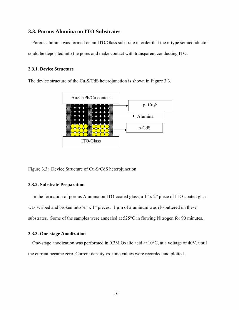
3.3.1. Device Structure The device structure of the Cu2S/CdS heterojunction is shown in Figure 3.3.
Figure 3.3: Device Structure of Cu2S/CdS heterojunction
3.3.2. Substrate Preparation
In the formation of porous Alumina on ITO-coated glass, a 1” x 2” piece of ITO-coated glass
was scribed and broken into ½” x 1” pieces. 1 µm of aluminum was rf-sputtered on these
substrates. Some of the samples were annealed at 525°C in flowing Nitrogen for 90 minutes.
3.3.3. One-stage Anodization
One-stage anodization was performed in 0.3M Oxalic acid at 10°C, at a voltage of 40V, until
the current became zero. Current density vs. time values were recorded and plotted.
p- Cu2S
Alumina
n-CdS
Au/Cr/Pb/Cu contact
ITO/Glass
16

3.3.4. Two-stage Anodization
Two-stage anodization was performed in 0.3M Oxalic acid at 10°C, at a voltage of 40V.
During the first stage, pores were allowed to form for 1 to 2 minutes; these were then partially
etched away in a 5%/2% Phosphoric/Chromic acid solution heated to 60°C. The remainder of the
initial pores served as pre-patterning for the longer second stage of anodization (re-anodization),
which was allowed to continue until the current spiked. After several minutes of re-anodization,
the current peaked indicating contact with the underlying ITO substrate. Samples were anodized
on both annealed and un-annealed substrates for varying duration. Current density vs. time
values were recorded and plotted.
3.4. Deposition of CdS Layer
CdS was deposited by two methods, electro-deposition and thermal evaporation. Deposition
was made on bulk samples and porous alumina templates.
3.4.1 Electro deposition of Bulk CdS
CdS nanocrystals were prepared by electrochemical deposition in dimethyl sulfoxide (DMSO)
solution composed of 0.055M CdCl2 and 0.19M elemental sulfur. The temperature was
maintained at 120°C. A 10V dc voltage was applied between the working electrode and the
platinum counter electrode. Electro-deposition was performed for different durations in order to
calculate the deposition rate.
3.4.2 Electro deposition of CdS into Porous Alumina
CdS nanocrystals were prepared by electrochemical deposition in dimethyl sulfoxide (DMSO)
solution composed of 0.055M CdCl2 and 0.19M elemental sulfur. The temperature was
17

maintained at 120°C. A 36V dc voltage was applied between the working electrode and the
platinum counter electrode in order to overcome the residual barrier layer seen at the bottom of
the pores. Current density vs. time values were recorded and plotted.
3.4.3 Thermal evaporation of CdS
Cadmium sulfide was used as the n-type material for the p-n heterojunction. CdS was
fabricated by thermal evaporation. Polycrystalline films of CdS were fabricated on ITO-coated
glass substrates by thermal evaporation of CdS powder. Evaporation grade CdS powder of
99.9% purity was purchased from AlfaAesar.
Thermal evaporation was performed on both bulk samples and porous alumina templates in the
same process. For bulk samples, the cleaned ITO-coated glass substrate was mounted on a disc
on the thermal evaporator. A portion of the substrate was masked with aluminum foil in order to
provide contact to ITO. For nano-scale heterojunction samples, the ITO-coated glass substrates
were covered with aluminum foil masks with round openings. This confined the CdS films to an
area well away from the edges of the ITO coated glass substrate, thereby preventing the
possibility of films grown on top of CdS shorting with ITO.
The quartz crystal monitor head was positioned close to the substrates. Cadmium sulfide
powder was loaded into a molybdenum boat and covered with glass wool. The presence of the
glass wool ensured that finer particles of CdS evaporate onto the ITO-coated glass substrate, and
kept large grains of CdS from ejecting from the boat prematurely. After loading CdS, the
vacuum chamber was closed and the thermal evaporator was allowed to pump down. Once the
pressure inside the chamber went down to 4x10⁻⁶ Torr, the molybdenum boat was heated by
passing current through the two ends clipped to the evaporation source. This process heats up the
18

CdS powder and starts the deposition of CdS onto ITO. A constant current was passed in order to
maintain a uniform deposition rate. Once the thickness of the film reached the desired thickness,
the current source was turned off and the deposition was stopped. The vacuum chamber was
allowed to cool down for one hour, then vacuum was broken by letting air into the chamber. The
samples were then removed from the chamber and stored in an air-tight container.
3.4.4 Annealing CdS
The cadmium sulfide films deposited by thermal evaporation were subjected to an
annealing treatment in a nitrogen atmosphere. Annealing is a process wherein the films are
heated at a very high temperature in a 3-zone quartz furnace tube in an atmosphere of a preferred
gas. The annealing process helps in re-crystallizing the CdS film and hence improves the film
adhesion and grain size. The quartz furnace tube consisted of an inlet for nitrogen, attached to a
nitrogen cylinder at one end and an outlet for nitrogen at the other end. The nitrogen outlet tube
was kept immersed in a bottle containing water. The samples were placed in the middle zone of
the furnace. Prior to heating the sample, the quartz furnace tube was purged with flowing
nitrogen for duration of 25 minutes to remove any oxygen present in the tube. This was an
important step, as any resident oxygen in the chamber could oxidize the sample during heating.
After purging, the sample was heated at a temperature of 450oC for 90 minutes. The furnace was
then switched off and allowed to cool down to room temperature. Finally the sample was
removed from the quartz furnace tube.
19

3.5 Deposition of CuCl layer and formation of heterojunction
3.5.1 Thermal evaporation of CuCl
A uniform film of cuprous chloride (CuCl) was deposited on top of the annealed CdS
film by thermal evaporation. Copper (I) chloride of 99.999% purity was purchased from
AlfaAesar. The commercially bought Copper (I) chloride is green in color due to the reaction
with atmospheric oxygen. The CuCl was bleached in a dilute 10% hydrochloric acid solution,
and then rinsed with acetone.
The powder was then placed in a molybdenum boat and loaded into the thermal evaporator.
The pressure inside the thermal evaporator was maintained close to 4x10⁻⁶ Torr. Aluminum foil
masks with small circular holes were wrapped on top of the CdS films. This was done to make
sure that the heterojunction was confined to a smaller area in order to get a realistic estimate of
short circuit currents. The CdS films were loaded onto a circular disc at the top of the chamber.
A current in the order of 2.5A was passed through the boat. The thermal evaporation process was
carried out as described earlier.
3.5.2 Formation of CdS/Cu2S heterojunction
The CuCl layer deposited must react with the CdS layer in order to form CuxS. Post-deposition
vacuum anneal was done in the vacuum chamber following the CuCl deposition. The following
reaction takes pace as a result of heating the substrates.
CdS + 2 CuCl Cu2S + CdCl2
The substrate temperature was heated to a temperature in the range of 190 oC – 200 oC with the
help of a quartz lamp fitted inside the vacuum chamber. Once the temperature in the chamber
stabilized around 190 oC, the substrates were heated for duration of 18 minutes. The heat source
was then switched off and the chamber was allowed to cool down to 45oC. The chamber was
20

finally vented to remove the samples. The resulting thickness of CuxS was about 0.7 microns, a
thickness sufficient enough to absorb the incident radiation.
Prior to rinsing to remove residual chlorides, the photovoltaic cells were measured for
probe voltages with a multimeter in order to get a rough estimate of the open circuit voltage.
Following the post-heat treatment, the photovoltaic cells were rinsed in order to remove the
residual chlorides and other reaction products. The photovoltaic cells were first immersed in a
beaker containing de-ionized water then rinsed in running de-ionized water to wash away the
residual CdCl2 and other byproducts of the reaction. After the rinse, the samples were dried in
flowing nitrogen and again measured for probe voltage.
3.5.3 Deposition of contacts
60 nm of gold was deposited by thermal evaporation as a top contact on the bulk samples.
3.6 Field Emission Scanning Electron Microscope (FE-SEM) Imaging
FE-SEM was used to characterize top views and cross sections of porous alumina on
molybdenum and ITO substrates. Images were also used to determine depth needed for
deposition of CdS and Cu2S, and to indicate whether deposition had filled the pores.
FE-SEM uses a beam of electrons generated by a field emission source to scan the surface of
the sample. These electrons are generated in an electron gun and are accelerated in a column
with a high electrical field gradient. The electron gun is usually housed on top of the column,
which is maintained in vacuum to prevent deflection of electrons. When the electrons bombard
the sample, a variety of signals are generated, such as secondary electrons, back-scattered
electrons, light, heat, and transmitted electrons. Secondary electrons are the electrons from the
21

sample. Surface structure of the sample can be understood from the angle and velocity of the
secondary electrons.
The test sample must be mounted on a clean SEM stub. First the stub is cleaned with acetone
and methanol, then allowed to dry in air. Next, a small (<2mm x 6mm) piece of the sample is
cut with a diamond scribe, and placed on a piece of conducting graphite tape which is used to
secure the specimen to the stub. Colloidal graphite is applied around the (glass) edges of the
sample to improve conductivity between the metal stub and the sample surface. To further
increase conductivity, the entire sample is sputter-coated with gold/palladium before being
placed in the SEM chamber.
The stub is placed into the specimen holder in one of three grooves depending on substrate
thickness. Once the stub is placed in the proper groove, the screw is tightened and the specimen
holder is placed into the specimen exchange chamber, following standard procedures.
The sample is brought into standard position, focused with low magnification, then with high
magnification. Aperture alignment and stigmator adjustment are performed at high
magnification (400kx). Images were saved in .tif format. Both top view and cross-sections of
the pores were taken.
3.7 J-V Setup
The J-V setup was controlled with a computer interface using Labview. Two Keithley
multimeters were used as the voltmeter and ammeter. The Labview software swept the dc
voltage from -0.4 to +0.8 V at a specified time interval in increments of 0.1V.
A solar simulator was used to provide light to the solar cells. The illumination from the bulb is
a standard one-sun with corresponding incident power of 100mWcm-2.
22

Probe voltages of the devices were measured with a handheld multimeter before and after
rinsing away residual chlorides, before contacts were deposited.
Baseline J-V curves were taken on bulk samples and silicon solar cells, but nano-porous
heterojunctions were only able to be measured by probe voltage, because the process of rinsing
away the chloride byproducts destroyed the samples.
23

Chapter 4: Nanoporous Alumina on Molybdenum Substrate Results 4.1 Preparation
The method of preparation was described in section 3.2 and is repeated below for convenience.
First, 1” x 2.25” glass slides were ultrasonically cleaned in acetone and methanol, baked at
100°C for 10 minutes and sputtered with approximately 400 nm of molybdenum. Thickness was
monitored with a quartz crystal and calibrated with a profilometer. Sheet resistance was
measured by four-point probe. Samples were dusted off with flowing nitrogen, then deposited
with approximately 2 µm of aluminum in the e-beam evaporator. Average deposition rate was
5.7 Å/second. The glass slide was scribed and broken into ½” x 1” pieces. Some aluminum
films were annealed while others were not.
4.2 Two-stage Anodization of Aluminum on Molybdenum-coated Glass Substrate in Oxalic Acid
Each piece was anodized for 1-2 minutes at 40 V, which resulted in anodized alumina pores on
the Molybdenum substrate. This step was followed by an etch in 5%/2% Phosphoric/Chromic
acid, to pre-pattern the pores for better order during second anodization. The second anodization
was performed at 40V, until the current peaked, indicating that a path for the ions to the
conducting molybdenum substrate had been created. Because the process was continued until
the aluminum layer was completely anodized, thickness of the porous alumina layer depended on
the initial thickness of the aluminum pre-cursor rather than on duration of anodization.
Anodization time ranged from 30 min. to 79 min., and depended on current density and other
factors such as the distance between the anode and the cathode during the anodization process.
24

4.3 Film Characteristics
SEM images of the cross-section and top view of alumina nano-pores fabricated on a
molybdenum substrate by two-stage anodization are shown in Figure 4.1 (Sample# 1_MOLY).
(a) (b) Figure 4.1: Alumina on molybdenum-coated glass substrate (1_MOLY) after two-stage
anodization in 0.3M Oxalic Acid, Sample Blank ‘M’. First anodization lasted 1 minute, re-anodization lasted 46 minutes. (a) SEM image of cross-section (b) SEM image of top view
The variation of current density with time of the anodization process is shown in Figure 4.2.
25

0.00
10.00
20.00
30.00
40.00
50.00
60.00
0 5 10 15 20 25 30 35 40 45 50 Time (min)
Cur
rent
den
sity
(A/s
q m
)
Beginning of 2nd Stage Anodization
Figure 4.2: Current density vs. time characteristics for two-stage anodization of Aluminum on
Molybdenum-coated glass substrate in 0.3M Oxalic Acid, sample no. 1_MOLY
The cross-section shows vertical pores extending to substrate. The top view shows pores of an
average width of 45 nm. Current density vs. time characteristic in Figure 4.2 shows steady
current density of between 21 and 25 A/sq. m during most of the re-anodization, until a final
spike, which indicates contact with the conducting substrate after complete anodization of
available aluminum.
4.4 Barrier Layer
At least two semiconductor layers, such as CIS and CdS, need to be electrodeposited inside the
alumina pores to fabricate a heterojunction solar cell. Furthermore, CIS needs to make good
contact with molybdenum. It is therefore essential that the anodization process is complete and
no aluminum or aluminum oxide is left on the Molybdenum substrate at the bottom of the pore.
To study the nature of incomplete anodization, we deposited (e-beam evaporation) an aluminum
26
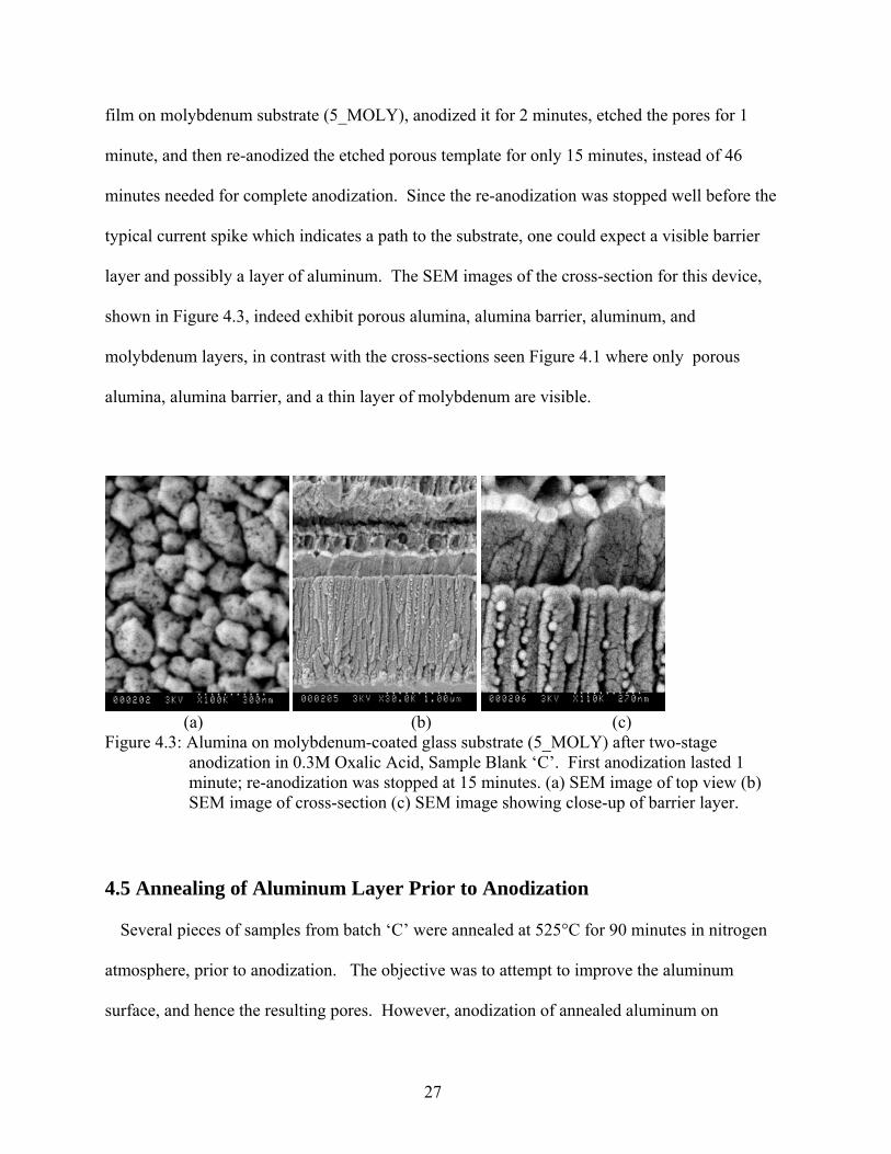
film on molybdenum substrate (5_MOLY), anodized it for 2 minutes, etched the pores for 1
minute, and then re-anodized the etched porous template for only 15 minutes, instead of 46
minutes needed for complete anodization. Since the re-anodization was stopped well before the
typical current spike which indicates a path to the substrate, one could expect a visible barrier
layer and possibly a layer of aluminum. The SEM images of the cross-section for this device,
shown in Figure 4.3, indeed exhibit porous alumina, alumina barrier, aluminum, and
molybdenum layers, in contrast with the cross-sections seen Figure 4.1 where only porous
alumina, alumina barrier, and a thin layer of molybdenum are visible.
(a) (b) (c) Figure 4.3: Alumina on molybdenum-coated glass substrate (5_MOLY) after two-stage
anodization in 0.3M Oxalic Acid, Sample Blank ‘C’. First anodization lasted 1 minute; re-anodization was stopped at 15 minutes. (a) SEM image of top view (b) SEM image of cross-section (c) SEM image showing close-up of barrier layer.
4.5 Annealing of Aluminum Layer Prior to Anodization
Several pieces of samples from batch ‘C’ were annealed at 525°C for 90 minutes in nitrogen
atmosphere, prior to anodization. The objective was to attempt to improve the aluminum
surface, and hence the resulting pores. However, anodization of annealed aluminum on
27

molybdenum-coated glass substrate from sample batch ‘C’ yielded pores which were not of high
quality. Figure 4.4 shows a micrograph of these pores in sample # 7_MOLY (average pore
width, 20 nm).
Figure 4.4: Annealed Alumina film on Molybdenum-coated glass substrate after two-stage
anodization in 0.3M Oxalic Acid, Sample Blank ‘C’. SEM image of top view of 7_MOLY. First anodization lasted 1 minute; re-anodization lasted 80 minutes
Several samples burned out early in the anodization process. Thus, yields for porous alumina
made on pre-annealed Aluminum on molybdenum-coated glass substrates was low and pores
were of inferior quality compared to pores on substrates which were not pre-annealed, where the
yield was 100%.
28
Chapter 5: Nanoporous Alumina on ITO-Glass Substrate Results
The method of preparation was described in section 3.3 and is repeated below for convenience.
A one μm thick aluminum layer was deposited on ITO-coated glass slides. Experiments were
performed to compare different methods of depositing aluminum for this application. These
included d.c. sputtering, r.f. sputtering, thermal evaporation, and e-beam evaporation. Some
samples were annealed at 550 °C for 90 minutes in flowing nitrogen, while others were not.
Best results were obtained on aluminum films that were r.f. sputtered and annealed prior to
anodization. After cooling, samples were removed and anodized at 10 °C in 0.3M Oxalic acid.
5.1 Comparison of Two Anodization Schedules
Two anodization schedules were evaluated. The first one is called single-stage anodization;
the current density vs. time plot for this case is shown in Figure 5.2.
29

Typical One Stage Anodization: Current Density vs. Time
0.00
200.00
400.00
600.00
800.00
1000.00
1200.00
1400.00
1600.00
0 1 2 3 4 5 6 7 8 9 10 11 12 13 14
Time (min)
Cur
rent
den
sity
, J (A
/sq.
m)
Figure 5.2: 1 Stage Anodization: Current Density vs. Time (Sample 1_ITO)
The second one is called two-stage anodization. In this case the sample was anodized for two
minutes, and then the oxide layer was partially removed in a heated phosphoric/chromic acid
mixture. Next, the sample was re-anodized for approximately twenty minutes. Current density
vs. time plot for this case is shown in Figure 5.3.
30

Typical Two Stage Anodization: Current Density vs. Time
0.005.00
10.0015.0020.0025.0030.0035.0040.0045.0050.0055.0060.0065.0070.0075.0080.0085.0090.0095.00
100.00105.00110.00115.00
0 1 2 3 4 5 6 7 8 9 10 11 12 13 14 15 16 17 18 19 20 21 22 23
Time (min)
Cur
rent
den
sity
(A/s
q m
)
Beginning of 2nd Anodization
Figure 5.3: 2 Stage Anodization: Current Density vs. Time (Sample 7_ITO)
The one-stage anodization resulted in rapid increase in current, possibly with localized pores at
the air/electrolyte interface. The bulk of the sample did not contain pores; this is illustrated in
Figure 5.4.
Figure 5.4: SEM micrograph of surface after one-stage anodization (Sample 1_ITO)
31

Two-stage anodization process resulted in pores that went all the way through and a steady
current flowed for several minutes. This is illustrated in Figures 5.5a and 5.5b.
Figure 5.5(a)
Figure 5.5(b) Figure 5.5(c) Figure 5.5 (d) Figure 5.5: SEM micrograph of surface after two-stage anodization on (a) top view, annealed
(Sample 6_ITO), (b) cross-section, annealed (Sample 6_ITO), (c) top view, unannealed (Sample 3_ITO), (d) cross-section unannealed (Sample 3_ITO)
32

5.2 Importance of Annealing Aluminum Layer Prior to Anodization
Figures 5.5(c) and 5.5(d) show the results when the aluminum layer was not annealed prior to
anodization. It was observed that better pores are obtained when aluminum is annealed.
Annealed, r.f.-sputtered substrates produced smoother aluminum films that, in turn, resulted in
better porous alumina templates; the pores were straighter and the surface was smoother.
Unannealed, r.f. sputtered substrates produced porous alumina that started with a rough, uneven
surface. Pores grew in a direction perpendicular to the uneven electrolyte/aluminum interface,
resulting in slanted pores and uneven pore surfaces.
33

Chapter 6: Deposition of CdS in Nanopores Results
The method of preparation was described in section 3.4 and is repeated below for convenience.
n-CdS was deposited by electro deposition as well as by thermal evaporation. A one µm thick
porous alumina on ITO-coated glass (5_ITO) was placed in a solution composed of dimethyl
sulfoxide (DMSO), 0.055M CdCl2 and 0.19M elemental sulfur at 120 ºC. 36V DC voltage was
applied between the working electrode and the platinum counter electrode for 10 minutes. A plot
of the current density vs. time characteristics for this process is shown in Figure 6.1.
CdS deposited in Porous Alumina on ITO Substrate
0.00
20.00
40.00
0 1 2 3 4 5 6 7 8 9 10 11Time (min)
Cur
rent
den
sity
(A/s
q m
)
As measured Correction for Porosity
Figure 6.1: Current density vs. time for CdS electro deposition in nanopores of alumina
34

The current density dropped to zero after electrodepositing CdS for 10 minutes; this indicated
that the electrodeposited CdS in the pore was relatively resistive. To investigate the resistive
nature of electro-deposited CdS further, CdS was electrodeposited onto the bulk ITO-coated
glass substrate. The current density vs. time characteristic for this process is shown in Figure
6.2.
0 5
10
15
20
25
30
35
40
45
50
0 2 4 6 8 10 12 14 Time (min)
Cur
rent
den
sity
, J (A
/sq.
m)
Figure 6.2: Current density vs. time – CdS electro deposition on bulk ITO-glass substrate
Again, the current density decreased with time; however it did not fall to zero. The initial
current density was also much larger than for the previous case. This is thought to be partially
due to full access to conducting ITO in the bulk case, as against the porous alumina substrate
which has 1 µm long pores of diameter 60 nm and interpore spacing of 90 nm. When comparing
current density of the device against the current density of the bulk sample, the sample size and
porosity of the device must be taken into consideration. Porosity was calculated to be 44% by
35

taking the ratio of the area of a pore to the area of the square bounded by the size of the interpore
spacing.
Another difference is that the device size was ½” x 1”, while the bulk sample was 1” x 1”,
twice the size of the device. The ratio of the bulk sample area to the area of device 5_ITO is
4.54, yet the ratio of their starting current is 7.25, so there must be another barrier to electro
deposition in the nanostructured design. It is known that in this device, a residual thin alumina
barrier layer between CdS and ITO remained after anodization. The CdS electro deposition
occurred through micro-cracks in the barrier layer, which would reduce the available device area
even further. This low area of contact between ITO and CdS is thought to be the reason for high
series resistance and very small currents in I-V measurements of the heterojunctions, so far.
The SEM image of the particles in the pores is shown in Figure 6.3. CdS appears as a vertical
series of interconnected dots inside the anodized aluminum oxide (AAO) pore.
Figure 6.3: SEM image of fracture section showing CdS electrodeposited in the AAO pores of
sample 5_ITO, before annealing. Average diameter of CdS particles was 20-30nm.
The typical diameter of CdS particles is 20-30 nm. An investigation into the effects of
annealing and cadmium chloride treatments on the CdS nanostructures in the pores would yield
more insight into these structures.
36

Chapter 7: CdS/Cu2S Junction Results
In preliminary experiments, Cu2S/CdS heterojunctions were fabricated inside the alumina
pores. The method of preparation was described in section 3.5 and is repeated below for
convenience. First, 1 μm thick CdS was electrodeposited in the pores as described above. The
samples were then annealed at 350 °C for 45 minutes in flowing nitrogen gas. Next, 1.1 μm of
CuCl was evaporated, and then annealed in vacuum at 195°C for 18 minutes. During this heat
treatment, the CuCl and CdS reacted to form CdCl2 and Cu2S.
It is shown in Table 7.1 that 1.1 μm of CuCl reacts with 1 μm of CdS, consuming 0.7 μm of
CdS and forming 0.67 μm of Cu2S. Because the initial thickness of the porous alumina was 1
μm, after the chemical reaction described above, the hetero-junction is formed inside the pores.
37

Table 7.1: Deposition thickness calculations
Under one-sun irradiation, an open-circuit voltage of 242 mV was observed (see Table 7.2) in
the photovoltaic Cu2S/CdS junction fabricated in the manner described above. Further
experiments are needed to better understand the formation of the Cu2S/CdS junction, improve
cell performance, and next, to investigate the CIS/CdS junction in nanopores.
38
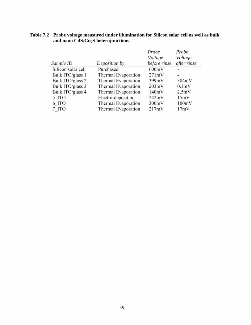
Table 7.2 Probe voltage measured under illumination for Silicon solar cell as well as bulk and nano CdS/Cu2S heterojunctions
Sample ID Deposition by
Probe Voltage before rinse
Probe Voltage after rinse
Silicon solar cell Purchased 600mV - Bulk ITO/glass 1 Thermal Evaporation 271mV - Bulk ITO/glass 2 Thermal Evaporation 399mV 384mV Bulk ITO/glass 3 Thermal Evaporation 203mV 0.1mV Bulk ITO/glass 4 Thermal Evaporation 140mV 2.5mV 5_ITO Electro-deposition 242mV 15mV 6_ITO Thermal Evaporation 300mV 100mV 7_ITO Thermal Evaporation 217mV 17mV
39

Chapter 8: Conclusion and Suggestions for Future Work 8.1 Conclusions
Nanoporous alumina films were formed on molybdenum as well as on indium tin oxide (ITO)
substrates. Effects of process parameters on the quality of porous alumina films were
investigated. For both molybdenum and ITO cases, oxalic acid was used as the electrolyte for
anodization and the 2-step anodization yielded better results than 1-step anodization. In case of
molybdenum substrates, average pore diameter was 45 nm when an anodization voltage of 40
volts was used for approximately 46 minutes; current density was approximately 23 Amps/sq. m
and annealing of aluminum prior to anodization was not beneficial. In case of ITO substrates,
pores of 45 nm diameter were obtained for approximately 20 minute anodization at 40 V; current
density was 40 Amps/sq. m; annealing of aluminum layer prior to anodization, at 525oC for 90
minutes was essential to getting good pores in the AAO film.
With the objective of making photovoltaic heterojunctions inside nanopores, a 1 micron thick
CdS layer was electrodeposited inside the pores of the alumina film on the ITO substrate. Also,
in preliminary experiments, CdS/Cu2S photovoltaic heterojunctions were formed by a chemical
reaction between CdS and CuCl. These exhibited an open circuit voltage of 242 mV under one-
sun illumination.
40
8.2 Suggestions for Future Work
Deposition of semiconductors such as CdS, and Cu2S and CIS inside the AAO pores needs
to be investigated in detail and the materials inside the pores characterized with the objectives of:
(i) improving the quality of the semiconductor films in the AAO pores, (ii) tailoring the
characteristics of the semiconductor films in the AAO pores, (iii) improving the quality of the
heterojunctions inside the pores, and (iv) making efficient photovoltaic cells inside the AAO
pores.
41
REFERENCES [1] D. M. Chapin, C.S.F., and G. L. Pearson, A New Silicon p-n Junction Photocell for Converting Solar Radiation into Electrical Power. J. Appl. Phys., 1954. 25: p. 676. [2] D. C. Reynolds, G.L., L. L. Antes, and R. E. Marburger, Photovoltaic Effect in Cadmium Sulfide. Phys. Rev., 1954. 96: p. 533. [3] Y. Hashimoto, N. Kithara, T. Negami, N. Nishitani and T. Wada Solar Energy Materials and Solar Cells, 50 (1998) 71-77. [4] Friedrich Kessler and Dominik Rudmann Solar Energy, 77 ( 2004) 685-695. [5] Jehad AbuShama , R. Noufi, S. Johnston, S. Ward, X. Wu, Conference Record of the Thirty-First IEEE Photovoltaic Specialist Conference (IEEE Cat. No. 05CH37608) (2005) 299-302. [6] R. Wieting, R. Gay, H. Nguyen, J. Palm, C. Rischmiller, A. Seapan, D. Tamant, D. Willett, Conference Record of the Thirty-First IEEE Photovoltaic Specialist Conference (IEEE Cat. No. 05CH37608) (2005) 177-82. [7] A. Gupta, A.D. Compaan, Conference Record of the Thirty-First IEEE Photovoltaic Specialist Conference (IEEE Cat. No. 05CH37608) (2005) 235-8 2005. [8] B.E. McCandless, R.W. Birkmire, Conference Record of the Thirty-First IEEE Photovoltaic Specialist Conference (IEEE Cat. No. 05CH37608) (2005) 398-401. [9] V.P. Singh, and J. McClure, Solar Energy Materials and Solar Cells, 76 (2002) 369-385. [10] Vijay P. Singh, David L. Linam, David D. Dils, John C. McClure and G. B. Lush, Solar Energy Materials and solar Cells, 63 (2000) 445-466. [11] S. Wagner, J.L. Shay, P. Migliorato and H. M. Kasper, Appl. Phy. Lett 25 (1975) 434. [12] B. M. Basol, V. K. Kapur and A. Halani, Proceedings of the 22nd IEEE PVSC, (1991) 893. [13] B. M. Basol, and V. K. Kapur, Proceedings of the 21st IEEE PVSC, (1990) 546. [14] B. M. Basol, V. K. Kapur and R. J. Matson, Proceedings of the 22nd IEEE PVSC, (1991) 1179. [15] B. M. Basol, V. K. Kapur, A. Halani, A. Minnick and C. Leidholm, Proceedings of the 23rd IEEE PVSC, (1993) 426. [16] N. Romeo, A. Bosio, V. Canevari and L. Zanotti, 7th E.C PV Solar Energy Conference, (1986) 656-61. [17] L. Chung Yang, G. Berry, L. J. Chou, G. Kenshole, A. Rockett, C. A. Mullan and C. J. Kiely, 23rd IEEE PVSC, (1993) 505-09. [18] Markus E. Beck, Michael Cocivera, Thin Solid Films, 272 (1996) 71-82. [19] M. S. Sadigov, M. Ozkan, E. Bacaksiz, M. Altunbas, A.I. Kopya, Journal of material Science, 34, (1999) 4579-84. [20] F. J. Garcia, M. S. Tomar, Proceedings of the 14th Conference on Solid State Devices, 1982. [21] A. P. Alivisatos, Journal of Physical Chemistry, 100 (1996) 13226-13239. [22] W. Palz, J. Besson, T. D. Nguyen and J. Vedel, Proceedings of the 9th IEEE PVSC, (1972) 91. [23] L.D. Partain, R. A. Schneider, L. F. Donaghey and P. S. McLeod, Journal of Applied Physics, 57 (1985) 5056. [24] A. M. Al-Dhafiri, G. J. Russell and J. Woods, Semicond. Sci. Technol 7 (1992) 1052-57. [25] V. P. Singh, Proceedings of the 13th IEEE PVSC, Washington, D. C., (1978) 507-512. [26] V. P. Singh, US Patent No. 4,404,734, Method of Making a CdS/CuxS Photovoltaic Cell, Photon Power Inc., El Paso, 1983.
42

[27] A. M. Barnett, J. A. Bragagnolo, R. B. Hall, J. E. Phillips, and J. D. Meakin, Proceedings of the 13th IEEE PVSC, Washington, D. C., (1978) 419. [28] R. B. Hall and J. D. Meakin, Thin Solid Films, 63, (1979) 203. [29] E. Aperathitis, F. J. Bryant, C. G. Scott, Solar Energy Materials, 20 (1990) 15-28 . [30] J. A. Thornton, D. G. Cornog, W. W. Anderson, R. B. Hall, J. E. Phillips, Conference Record of the IEEE PVSC, (1982) 737-742. [31] R. B. Hall, R. W. Birkmire, J. E. Phillips and J. D. Meakin, Appl. Phys. Lett 38 (1981) 925. [32] K. Ernst, A. Belaidi, R. Konenkamp 18 (2003) 475-479. [33] R. Konenkamp , L. Dloczik, K. Ernst and C. Olesch, Physica E, 14,(2002) 219-23. [34] S. M. Sze, “Physics of Semiconductor Devices, 2nd edition,” John Wiley & Sons, 1981, pp. 790-838. [35]Chapter 6 ,Thin-Film Solar Cells Based on Nanostructured CdS, CIS, CdTe and Cu2S, Vijay P. Singh, R.S. Singh, and Karen E. Sampson, Nanostructured Materials for Solar Energy Conversion , T. Soga (editor). [36] Visweswaran Jayaraman, M.S. Thesis University of Kentucky, May 2005. [37] Kasturi Lal Chopra, Suhit Ranjan Das, Thin Film Solar Cells, 1983 Plenum Press, NewYork . [38] J.C. McClure, V.P. Singh, G.B. Lush, E. Clark, G.W. Thompson, Solar Energy Materials and Solar Cells, 55 (1998) 141-8. [38] V.P. Singh, J.C. McClure, G.B. Lush, W. Wang, X. Wang, G.W. Thompson, E. Clark, Solar Energy Materials and Solar Cells, 59 (1999) 145-61. [40] D.L. Linam, V.P. Singh, D.W. Dils, J.C. McClure, G.B. Lush, Proceedings of SPIE - The International Society for Optical Engineering, v 3975 (2000) 1258-1261. [41] H. Chavez, M. Jordan, J.C. McClure, G. Lush, V.P. Singh, Journal of Materials Science: Materials in Electronics, 8 (1997) 151-4. [42] O. Jessensky, F. Muller, and U. Gosele, “Self-organized formation of hexagonal pore arrays”, Appl. Phys. Lett., Vol. 72, No. 10, 9 March 1998. [43] S.Z. Chu, K. Wada, S. Inoue, S. Todoroki, Electrochimica Acta 48 (2003) 3147-3153. [44] S. Ono,* M. Saito, M. Ishiguro, and H. Asoh “Controlling Factor of Self-Ordering of Anodic Porous Alumina”, Journal of The Electrochemical Society, 151 8 B473-B478 2004.
43

Vita Karen was born on March 6, 1966, in Lexington, Kentucky. She earned her Bachelor’s in
Electrical and Computer Engineering from the University of Kentucky in December 2003. She
joined the Master’s program in Electrical and Computer Engineering at University of Kentucky
in January 2004. She worked as a Research Assistant in the Electronic Devices Research Lab at
University of Kentucky until May 2006. Currently she is working as a Design Engineer at
Hitachi Automotive Products, Harrodsburg, Kentucky. Her publications are listed below.
• “Porous Alumina Template and Nanostructured CdS for Thin Film Solar Cell Applications,” A. Aguilera, V. Jayaraman, V. Jayaraman, K. Sampson, S. Sanagapalli, R. S. Singh and V. P. Singh, Accepted for publication by Solar Energy Materials and Solar Cells, 90, pp. 713-726 (2006).
• Chapter 6 ,Thin-Film Solar Cells Based on Nanostructured CdS, CIS, CdTe and Cu2S,
Vijay P. Singh, R.S. Singh, and Karen E. Sampson, Nanostructured Materials for Solar Energy Conversion , T. Soga (editor) .
• “Analysis of CuPc-based Organic Solar Cell with High Photovoltage,” Alberto Aguilera, R. Suresh Singh, Balaji Parthasarathy, Karen E. Sampson, Subhash C.C. Vallurupalli, John E. Anthony, Marcia M. Payne, and Vijay P. Singh, Proceedings of 31st IEEE Photovoltaic Specialists Conference, January 2005.
• “Numerical Simulation of Field, Current and Luminance in SrS:Cu, Ag ACTFEL Display
Devices,” Praveen Sivakumar, Alberto Aguilera, Dharmashankar Rajagopalan, Karen Sampson, Vijay P. Singh*, submitted to IEEE Transactions on Electron Devices.
Karen E. Sampson November 16, 2006
44