nanoscale silica capsules ordered on a substrate: oxidation of nanocellular thin films of...
TRANSCRIPT
Silica Nanostructures
DOI: 10.1002/anie.200602274
Nanoscale Silica Capsules Ordered on aSubstrate: Oxidation of Nanocellular Thin Filmsof Poly(styrene-b-dimethylsiloxane)**
Lei Li and Hideaki Yokoyama*
The fabrication of nanoscale hollow particles has beenreceiving increasing attention in both academic and industrialfields. Various materials have been adopted to satisfy thegrowing needs for encapsulation,[1, 2] and a variety of chemicaland physicochemical methods have been developed in orderto prepare hollow spheres with controlled size and shape,including colloid particle templating,[3] sol–gel synthesis,[4]
layer-by-layer self-assembly,[5] and surface living polymeri-zation.[6] Block copolymers are considered to be idealcandidates for the fabrication of nanoscale structures, owingto their predictable self-assembly in the size range 5–50 nm.[7,8] Our group recently reported a nondestructiveCO2 foaming method that introduces 15–30-nm voids intoCO2-philic fluorinated block copolymers.[9–12] Herein, weextend the same methodology to poly(styrene-b-dimethylsi-loxane) (PS-PDMS), the PDMS domain of which is a CO2-philic polymer,[13] to fabricate nanocells in thin films and toconvert them into silica hollow particles (nanocapsules)ordered on substrates by oxidation.[14] Silica nanocapsuleswith a number density of 7.0 5 1010 cm�2, a diameter of lessthan 40 nm, and a wall thickness of 2 nm were successfullysynthesized.
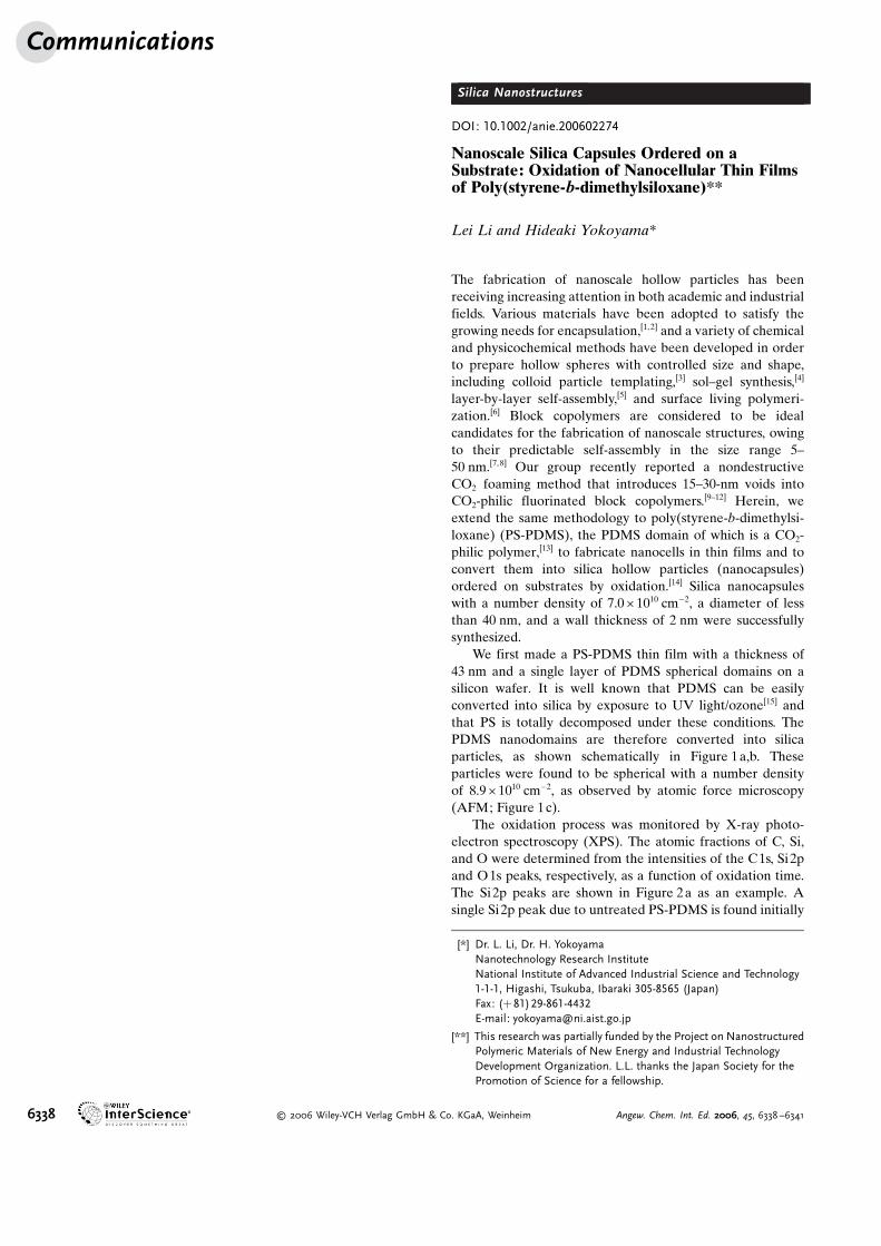
We first made a PS-PDMS thin film with a thickness of43 nm and a single layer of PDMS spherical domains on asilicon wafer. It is well known that PDMS can be easilyconverted into silica by exposure to UV light/ozone[15] andthat PS is totally decomposed under these conditions. ThePDMS nanodomains are therefore converted into silicaparticles, as shown schematically in Figure 1a,b. Theseparticles were found to be spherical with a number densityof 8.9 5 1010 cm�2, as observed by atomic force microscopy(AFM; Figure 1c).
The oxidation process was monitored by X-ray photo-electron spectroscopy (XPS). The atomic fractions of C, Si,and O were determined from the intensities of the C1s, Si2pand O1s peaks, respectively, as a function of oxidation time.The Si2p peaks are shown in Figure 2a as an example. Asingle Si2p peak due to untreated PS-PDMS is found initially
[*] Dr. L. Li, Dr. H. YokoyamaNanotechnology Research InstituteNational Institute of Advanced Industrial Science and Technology1-1-1, Higashi, Tsukuba, Ibaraki 305-8565 (Japan)Fax: (+81)29-861-4432E-mail: [email protected]
[**] This research was partially funded by the Project on NanostructuredPolymeric Materials of New Energy and Industrial TechnologyDevelopment Organization. L.L. thanks the Japan Society for thePromotion of Science for a fellowship.
Communications
6338 � 2006 Wiley-VCH Verlag GmbH & Co. KGaA, Weinheim Angew. Chem. Int. Ed. 2006, 45, 6338 –6341
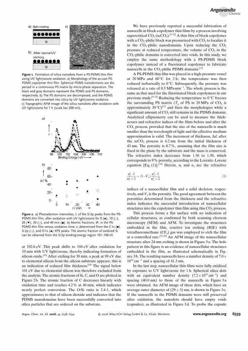
at 102.6 eV. This peak shifts to 104 eV after oxidation for10 min with UV light/ozone, thereby indicating formation ofsilicon oxide.[16] After etching for 30 min, a peak at 99 eV dueto elemental silicon from the silicon substrate appears; this isan indication of reduced film thickness.[16] The signal below101 eV due to elemental silicon was therefore excluded fromthe analysis. The atomic fractions of Si, C, andO are plotted inFigure 2b. The atomic fraction of C decreases linearly withoxidation time and reaches 4.2% at 40 min, which indicatesnearly perfect conversion. The O/Si ratio is 2.4:1, whichapproximates to that of silicon dioxide and indicates that thePDMS nanodomains have been successfully converted intosilica particles that are ordered on the substrate.
We have previously reported a successful fabrication ofnanocells in block-copolymer thin films by a process involvingsupercritical CO2 (scCO2).
[9–12] A thin film of block copolymerwith a CO2-philic block was pressurized with CO2 to localize itin the CO2-philic nanodomains. Upon reducing the CO2
pressure at reduced temperature, the volume of CO2 in theCO2-philic domains is converted into voids. In this study, weemploy the same methodology with a PS-PDMS blockcopolymer instead of a fluorinated copolymer to fabricatenanocells in the CO2-philic PDMS domains.[13]
A PS-PDMS thin film was placed in a high-pressure vesselat 20 MPa and 60 8C for 2 h; the temperature was thenreduced isobarically to 0 8C. Subsequently, the pressure wasreleased at a rate of 0.5 MPamin�1. The whole process is thesame as that used for the fluorinated block copolymers in ourprevious study.[9–12] Reducing the temperature to 0 8C freezesthe surrounding PS matrix (Tg of PS in 20 MPa of CO2 isapproximately 30 8C)[17] and fixes the morphologies while asignificant amount of CO2 still remains in the PDMS domains.Analytical ellipsometry can be used to measure the thick-nesses and refractive indices of the films before and after theCO2 process, provided that the size of the nanocells is muchsmaller than the wavelength of light and the effective mediumapproximation is valid. The increment of thickness, Dd, afterthe scCO2 process is 4.2 nm from the initial thickness of43 nm. The porosity is 8.7%, assuming that the film size isfixed in the plane by the substrate and the mass is conserved.The refractive index decreases from 1.56 to 1.50, whichcorresponds to 9% porosity, according to the Lorentz–Lorenzequation [Eq. (1)].[18] Herein, nf and ns are the refractive
n2f�1n2f þ 2
¼ ð1�VcÞn2s�1n2s þ 2
ð1Þ
indices of a nanocellular film and a solid skeleton, respec-tively, andVc is the porosity. The good agreement between theporosities determined from the thickness and the refractiveindex indicates the successful introduction of nanocellularstructures into the copolymer thin film using this CO2 process.
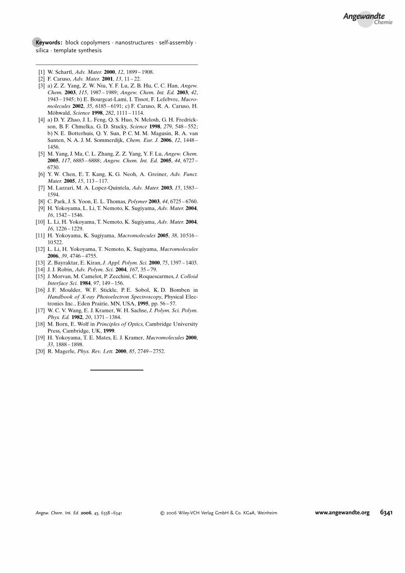
This process forms a flat surface with no indication ofcellular structures, as confirmed by both scanning electronmicroscopy (SEM) and AFM. To investigate the structuresembedded in the film, reactive ion etching (RIE) withtetrafluoromethane (CF4) gas was employed to etch the filmat a controlled rate.[19,20] An AFM image of the nanocellularstructure after 24-nm etching is shown in Figure 3a. The holepattern in this figure is an evidence of nanocellular structuresembedded in the film, as illustrated schematically in Fig-ure 3b. The resulting nanocells have a number density of 7.0 51010 cm�2 and a spacing of 41.3 nm.
In the last step, nanocellular thin films were fully oxidizedby exposure to UV light/ozone for 1 h. Spherical silica dotswith an equivalent number density (7.2 5 1010 cm�2) andspacing (40.0 nm) to those of the nanocells in Figure 3awere obtained. An AFM image of these dots, which have anaverage outer diameter of (29� 3) nm, is shown in Figure 3c.If the nanocells in the PDMS domains were still preservedafter oxidation, the nanodots should have empty voids(capsules), as illustrated in Figure 3d. To probe the capsule
Figure 1. Formation of silica nanodots from a PS-PDMS thin filmusing UV light/ozone oxidation. a) Morphology of the as-cast PS-PDMS copolymer thin film. Spherical PDMS nanodomains are dis-persed in a continuous PS matrix by micro-phase separation. Theblack and gray domains represent the PDMS and PS domains,respectively. b) The PS domains are decomposed, and the PDMSdomains are converted into silica by UV light/ozone oxidation.c) Topographic AFM image of the silica nanodots after oxidation withUV light/ozone for 1 h (scale bar 200 nm).
Figure 2. a) Photoelectron intensities, I, of the Si2p peaks from the PS-PDMS thin film, after oxidation with UV light/ozone for 0 (~), 10 (&),20 (!), 30 (*), and 40 min (*). b) Atomic fractions, F, in the PS-PDMS thin film versus oxidation time, t, determined from the C1s (&),Si 2p (*), and O1s (~) XPS peaks. The atomic fraction of oxidized Sican be obtained from the Si2p binding-energy region 101–106 eV.
AngewandteChemie
6339Angew. Chem. Int. Ed. 2006, 45, 6338 –6341 � 2006 Wiley-VCH Verlag GmbH & Co. KGaA, Weinheim www.angewandte.org

structure, the nanodots were etched for 2 min by RIE with aCF4 rate of 1.5 mLmin�1 and a powder density of 2 Wcm�2.Under these conditions, the etching rate for silica is1 nmmin�1, which means that 2 nm of the silica layer wasetched away from the surface. This etching removes the topskin of the capsules and converts them into calderas on thesubstrate, as shown in Figure 3e and illustrated in Figure 3 f.This caldera morphology is clear evidence of a capsulestructure before CF4 etching. The top wall thickness of thesilica nanocapsules is approximately 2 nm. The silica capsuleswere found to be tightly bound to the silicon substrate, evenafter a long ultrasonic rinse with organic solvents. Thissuccessful fabrication of silica nanocapsules provides strongevidence for the presence of CO2-philic domains surroundingthe voids.
In conclusion, we have synthesized silica nanocapsulesthat are ordered on a substrate by a nondestructive CO2-foaming method that produces nanocells with the help of ablock-copolymer template containing CO2-philic PDMS
domains. The nanocells are formed in the PDMS domains.The PDMS domains surrounding the empty cells are con-verted into hollow silica particles (nanocapsules) that areordered on the substrate by oxidation with UV light/ozone.These nanocapsules with a number density of 7.0 5 1010 cm�2
have a diameter less than 40 nm and a wall thickness of 2 nm.An advantage of this method over others for the synthesis ofnanocapsules is that the nanocapsules are two-dimensionallyordered and controlled using the domain structure of theblock-copolymer template. The capsules are easily embeddedby deposition after this process. The fabrication of morecomplex structures using the same method but with differentblock fractions is currently under investigation.
Experimental SectionA poly(styrene-b-dimethylsiloxane) block copolymer was purchasedfrom Polymer Source Inc. Themolecular weights of the PS and PDMSblocks are 57600 and 6500 gmol�1, respectively. The silicon waferswere used as received. The PS-PDMS copolymer films were preparedby spin-casting a toluene solution onto silicon substrates. The filmthickness was controlled by varying the concentration of the solutionsand the rotation speed.
A high-pressure vessel for CO2 processes was connected to aliquid chromatography pump (JASCO PU-2086 plus) fitted with acooling head and to a back-pressure regulator (JASCO SCF-Bpg).The PS-PDMS films were placed in the high-pressure vessel at 60 8Cfor 2 h at a CO2 pressure of 20 MPa. The vessel was then cooled to0 8C in an ice bath whilst maintaining the pressure by means of thepump and regulator. The depressurization rate was controlled at0.5 MPamin�1.
Oxidation of the copolymer thin films by exposure to UV light/ozone was performed in a UVO cleaner 342-101 (Jelight, Inc.). Thecleaner generates UV emissions at a wavelength of 254 nm(28 mWcm�2). The distance between the UV source and the siliconwafers was 50 mm.
The film thickness and refractive index were measured with aJASCOM-220 ellipsometer with incident light in a wavelength rangeof 400–800 nm at an incident angle of 608 with respect to the surfacenormal. The etching process to expose the embedded cellularstructures to the surface and open the hollow spherical structureswas performed with a reactive ion etcher (FA-1, SAMCO) andtetrafluoromethane (CF4) gas. Etching was performed with a CF4
flow rate of 2 mLmin�1, a pressure of 10 Pa, and a power density of10 Wcm�2. The etching rate for PS-PDMS copolymer thin films isapproximately 0.4 nms�1 under these conditions.
The surface topography due to the embedded cell structuresrevealed by RIE was characterized by AFM. AFM measurementswere carried out in the tappingmode with an SII SPA300HV.We useda cantilever with a carbon nanotube tip (SII Co.) for the nanocellularPS-PDMS films. Silicon cantilevers (DF-20, SII Co.) were used for theobservation of silica nanodots and nanocapsules.
XPS spectra were acquired with a PHI Quantum 2000 spectrom-eter usingmonochromated X-rays from anAlKa source with a take-offangle of 458 from the surface plane. The X-ray beam was operating at20 W and was focused to a diameter of about 100 mm rastered over a500 mm5500 mm area. The atomic fractions of carbon, oxygen, andsilicon were computed using the attenuation factors provided by thesupplier and the sum of these atomic fractions was normalized tounity.
Received: June 7, 2006Published online: August 25, 2006
Figure 3. Topographic AFM images and schematic pictures of silicacapsules on the substrate. a) Topographic image after RIE for 60 s(scale bar 100 nm), and b) schematic picture of the nanocellularstructures on the block-copolymer film. The black and gray domainsrepresent the PDMS and PS domains, respectively; the white part isair. c) Three-dimensional topographic image after oxidation by UVlight/ozone, and d) schematic picture of the silica nanocapsulesobtained. e) Three-dimensional topographic image after further RIE of2-nm, and f) schematic picture showing the resulting calderatopography.
Communications
6340 www.angewandte.org � 2006 Wiley-VCH Verlag GmbH & Co. KGaA, Weinheim Angew. Chem. Int. Ed. 2006, 45, 6338 –6341
.Keywords: block copolymers · nanostructures · self-assembly ·silica · template synthesis
[1] W. Schartl, Adv. Mater. 2000, 12, 1899 – 1908.[2] F. Caruso, Adv. Mater. 2001, 13, 11 – 22.[3] a) Z. Z. Yang, Z. W. Niu, Y. F. Lu, Z. B. Hu, C. C. Han, Angew.
Chem. 2003, 115, 1987 – 1989; Angew. Chem. Int. Ed. 2003, 42,1943 – 1945; b) E. Bourgeat-Lami, I. Tissot, F. Lefebvre,Macro-molecules 2002, 35, 6185 – 6191; c) F. Caruso, R. A. Caruso, H.MJhwald, Science 1998, 282, 1111 – 1114.
[4] a) D. Y. Zhao, J. L. Feng, Q. S. Huo, N. Melosh, G. H. Fredrick-son, B. F. Chmelka, G. D. Stucky, Science 1998, 279, 548 – 552;b) N. E. Botterhuis, Q. Y. Sun, P. C. M. M. Magusin, R. A. vanSanten, N. A. J. M. Sommerdijk, Chem. Eur. J. 2006, 12, 1448 –1456.
[5] M. Yang, J. Ma, C. L. Zhang, Z. Z. Yang, Y. F. Lu,Angew. Chem.2005, 117, 6885 – 6888; Angew. Chem. Int. Ed. 2005, 44, 6727 –6730.
[6] Y. W. Chen, E. T. Kang, K. G. Neoh, A. Greiner, Adv. Funct.Mater. 2005, 15, 113 – 117.
[7] M. Lazzari, M. A. Lopez-Quintela, Adv. Mater. 2003, 15, 1583 –1594.
[8] C. Park, J. S. Yoon, E. L. Thomas, Polymer 2003, 44, 6725 – 6760.[9] H. Yokoyama, L. Li, T. Nemoto, K. Sugiyama,Adv. Mater. 2004,
16, 1542 – 1546.[10] L. Li, H. Yokoyama, T. Nemoto, K. Sugiyama,Adv. Mater. 2004,
16, 1226 – 1229.[11] H. Yokoyama, K. Sugiyama, Macromolecules 2005, 38, 10516 –
10522.[12] L. Li, H. Yokoyama, T. Nemoto, K. Sugiyama, Macromolecules
2006, 39, 4746 – 4755.[13] Z. Bayraktar, E. Kiran, J. Appl. Polym. Sci. 2000, 75, 1397 – 1403.[14] J. J. Robin, Adv. Polym. Sci. 2004, 167, 35 – 79.[15] J. Morvan, M. Camelot, P. Zecchini, C. Roquescarmes, J. Colloid
Interface Sci. 1984, 97, 149 – 156.[16] J. F. Moulder, W. F. Stickle, P. E. Sobol, K. D. Bomben in
Handbook of X-ray Photoelectron Spectroscopy, Physical Elec-tronics Inc., Eden Prairie, MN, USA, 1995, pp. 56 – 57.
[17] W. C. V. Wang, E. J. Kramer, W. H. Sachse, J. Polym. Sci. Polym.Phys. Ed. 1982, 20, 1371 – 1384.
[18] M. Born, E. Wolf in Principles of Optics, Cambridge UniversityPress, Cambridge, UK, 1999.
[19] H. Yokoyama, T. E. Mates, E. J. Kramer,Macromolecules 2000,33, 1888 – 1898.
[20] R. Magerle, Phys. Rev. Lett. 2000, 85, 2749 – 2752.
AngewandteChemie
6341Angew. Chem. Int. Ed. 2006, 45, 6338 –6341 � 2006 Wiley-VCH Verlag GmbH & Co. KGaA, Weinheim www.angewandte.org