nanotechnology is the creation of useful/functional
TRANSCRIPT


Nanotechnology is the creation of USEFUL/FUNCTIONALmaterials, devices and systems through manipulation of matterat nanometer scale and exploitation of novel phenomenawhich arise because of the nanometer sizes.
-9


Physical Dimension
CPU Clock SpeedAverage Transistor “Price”
Component Density
$1 / transistor
100 Nano$ / transistor
x 107

Transistor can not be scaled forever Silicon is no longer the best computing material No device solution to deal with power dissipation crisis
Manufacturing cost will soar
Scientific and industry research communities are looking for: Technology that sustains the spirit of Moore’s Law Materials that are much better than silicon Devices that are more energy-efficient (e.g., non-charge-based) Fabrication processes that are much cheaper, self-controlled,
dependable, and sustainable
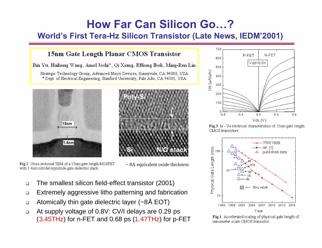
The smallest silicon field-effect transistor (2001) Extremely aggressive litho patterning and fabrication Atomically thin gate dielectric layer (~8Å EOT) At supply voltage of 0.8V: CV/I delays are 0.29 ps
(3.45THz) for n-FET and 0.68 ps (1.47THz) for p-FET
~ 8A equivalent oxide thickness

Fin-memory (2006)FinFET (2006)FinFET (2003) FinFET SRAM (2005)
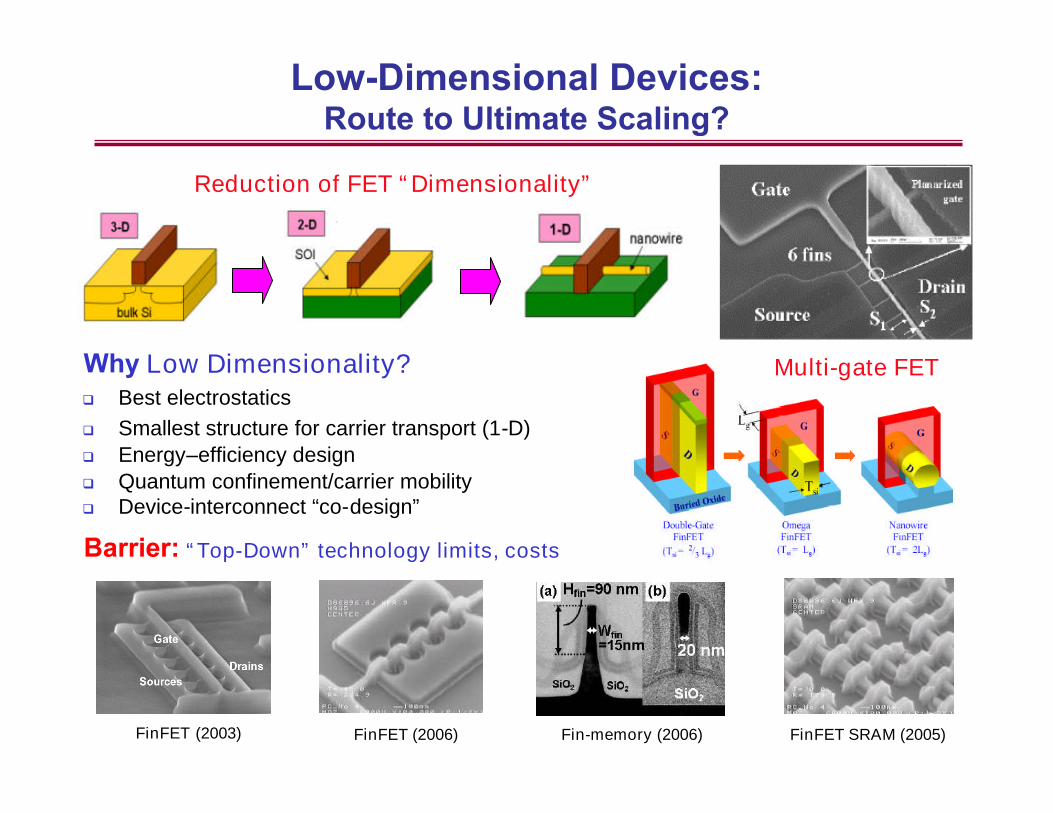
Low Dimensionality? Best electrostatics Smallest structure for carrier transport (1-D) Energy–efficiency design Quantum confinement/carrier mobility Device-interconnect “co-design”
“Top-Down” technology limits, costs
Reduction of FET “Dimensionality”
Multi-gate FET

Bio-mimeticmolecularcomputing
SNW/CNT devices
Bio-systemselectronics interface
Ultra highdensitystorage Computing Capacity
RLV
e-
Nano-electroniccomponents
Europa Sub
Robot ColonySensor Web
Nanotechnology is the “enabling technology” driving numerous applications. The core concept of “bottom-up” is to employ cheap chemistry to promote self-
assembly of functional components. New materials and technologies are emerging for energy-efficient information
processing devices.

Hierarchical AssemblyNano-systems
Inorganic CrystallineNanostructures
Organic/Bio MolecularNanostructures
tubewire
beltdisk
cubesaw
tetrapod combmonolayer wire
Singlemolecule
supramolecules
windmill
Self-assemblyNano-components
Crystal growth
Reaction chemistry Surface chemistryOrganic synthesis
Molecular engineeringMaterial synthesis

Solution-Phase Synthesis Solution-Liquid-Solid (SLS) Method Solvothermal Chemical Synthesis Template-Based Synthesis
Gas-Phase Synthesis Vapor-Liquid-Solid (VLS) Method
Laser ablation PVD CVD (thermal CVD, LPCVD,
PECVD, MOCVD) Vapor-Solid (VS) Method Oxide-Assisted Growth (OAG)

Thermal CVD
Thermal PVD


10+ types of low-dimensional nanostructures within five major categories:IV group elemental semiconductors (Si, Ge): computing/data storageIII-V group compound semiconductor (InSb): computing, spintronics, optoelectronics, TEMetal oxide (ZnO, TiO2): solar cell, spintronics, sensorsChalcogenides (GeTe, GeSb, Ge2Sb2Te5, Sb2Te3): phase-change memoryFerroelectric metal oxide (BaTiO3): data storage
Material characterizationPhysical morphology (SEM, TEM), chemical composition (EDS, XPS), crystal structure (XRD,EDP), thermal property (in-situ heating & TEM imaging)
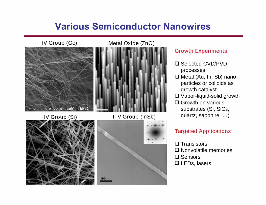
IV Group (Ge) Metal Oxide (ZnO)
IV Group (Si)
Growth Experiments:
Selected CVD/PVDprocesses
Metal (Au, In, Sb) nano-particles or colloids asgrowth catalyst
Vapor-liquid-solid growthGrowth on various
substrates (Si, SiO2,quartz, sapphire, …)
Targeted Applications:
TransistorsNonvolatile memoriesSensorsLEDs, lasers
III-V Group (InSb)

Gas Flow Rate

Catalyst Selection
Antimony (Sb) catalyst
Growth Orientations
Ge-NW
Ge-NWIndium (In) catalyst

Elemental Mapping of GeSb Nanowire
Ge Mapping Sb MappingGeSb TEM Image
EDSSAEDTEM
HR-TEM

STM tunneling current to measureGe nanowire band-gap
STM image of Ge nanowire
dI/dV

Energy-efficient, scalable, high-performance transistor
Nanoscale storage media to improve performance/density/energy-efficiency
High-efficiency solar cells & thermoelectrics
Lower detection threshold (2-4 orders) at molecular or atomic level
Component and assembly technology for future electronicsfeaturing transparency, disposability, and flexibility

4
Ge nanowire
NiGe source
NiGe drain


Si-BasedMemories
Nano-EngineeredStorage Devices
DisruptiveStorage Devices
Floating-Gate
Nanocrystal
Fin-Based Memory
MRAM
Phased-Change
Carbon Nanotube
Probe-Based
Polymer
Nanowire
Molecular
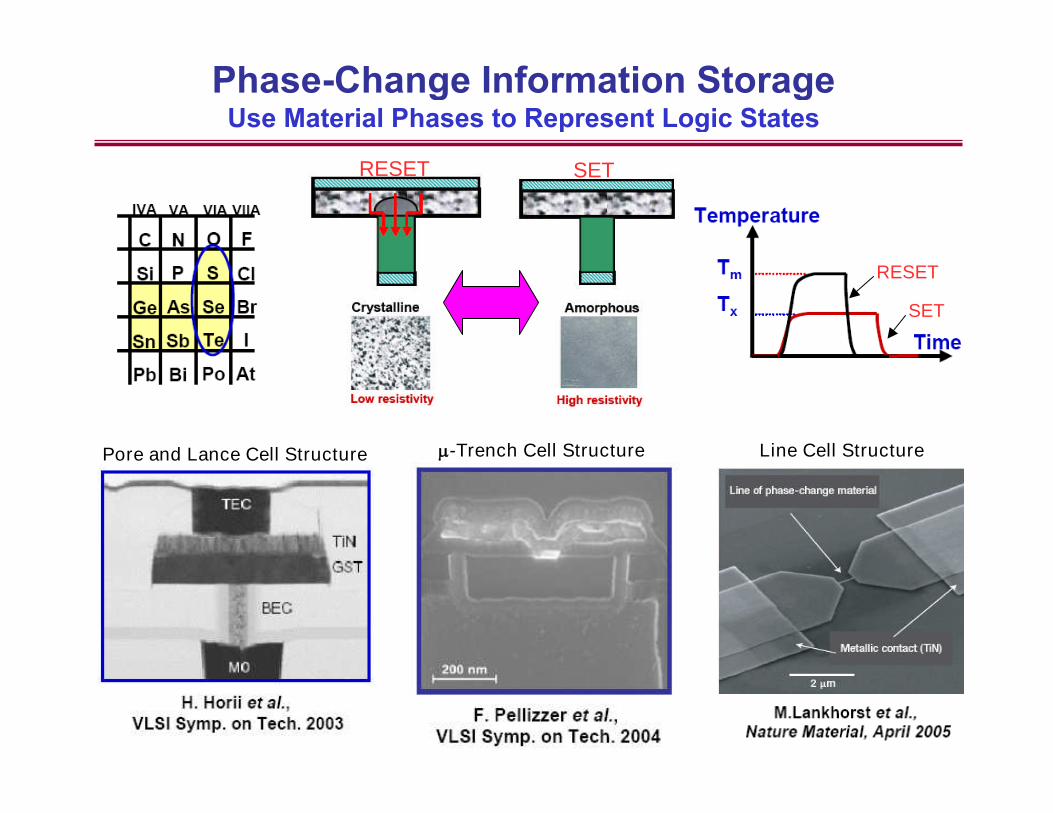
RESET SET
RESET
SET
Pore and Lance Cell Structure -Trench Cell Structure Line Cell Structure
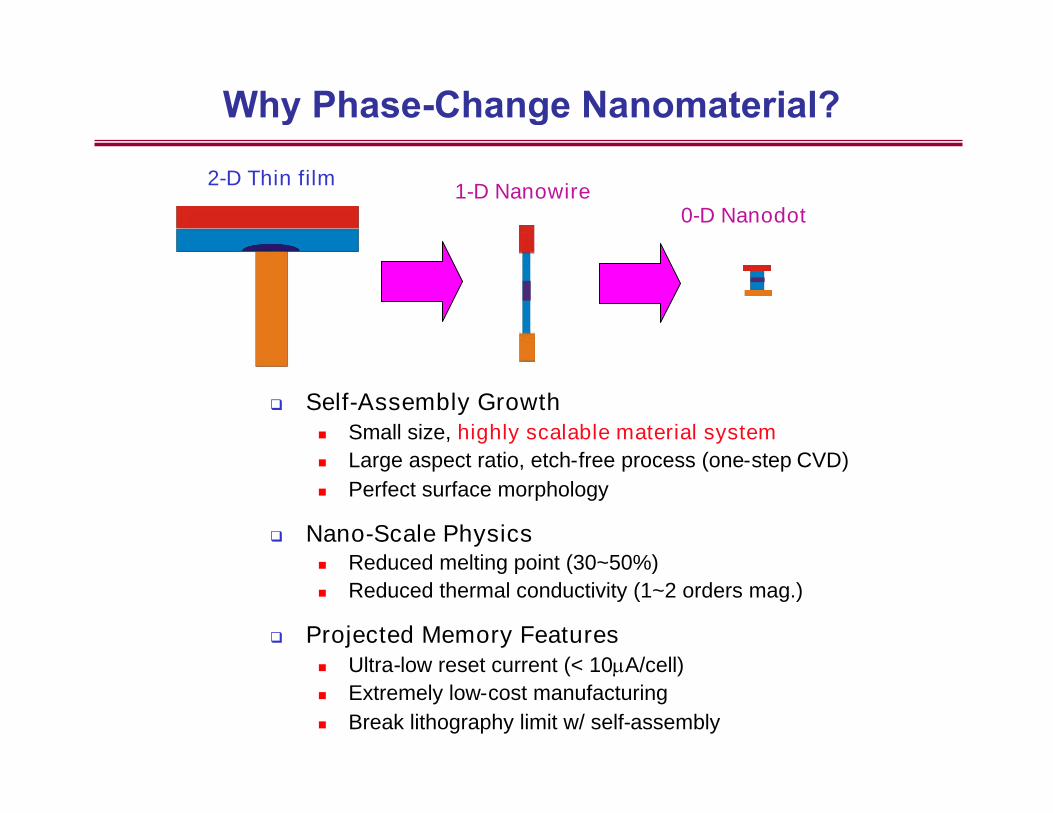
Self-Assembly Growth Small size, highly scalable material system Large aspect ratio, etch-free process (one-step CVD) Perfect surface morphology
Nano-Scale Physics Reduced melting point (30~50%) Reduced thermal conductivity (1~2 orders mag.)
Projected Memory Features Ultra-low reset current (< 10A/cell) Extremely low-cost manufacturing Break lithography limit w/ self-assembly
2-D Thin film1-D Nanowire
0-D Nanodot

InSb In2Se3Ge2Sb2Te5
GeTeSbTe

Tm of bulk PCM
Tm of PCM nanowires
• Melting temperature of phase-change nanowire is identified asthe point at which: (1) electrondiffraction pattern disappears, and(2) nanowire starts to evaporate.
• This property is nanowire diameter-dependent: more significantreduction at smaller diameters
24%46%% Reduction
680°C390°CNanowire Tm
890°C725°CBulk Tm
In2Se3GeTe

Thermally induced nanowire encodingwith scanning focused e-beam.

2 3

2/27/2008
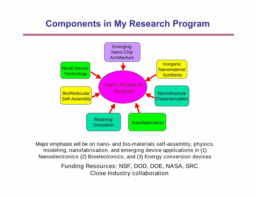
Nano-ResearchProgram
NanofabricationModelingSimulation
Novel DeviceTechnology
EmergingNano-Chip
Architecture
Bio/MolecularSelf-Assembly
InorganicNanomaterial
Synthesis
NanostructureCharacterization
Major emphasis will be on nano- and bio-materials self-assembly, physics,modeling, nanofabrication, and emerging device applications in (1)
Nanoelectronics (2) Bioelectronics, and (3) Energy conversion devices
Funding Resources: NSF, DOD, DOE, NASA, SRCClose Industry collaboration

High-PerformanceNanoelectronics
MaterialGrowth & Assembly
Nano-DevicePhysics
Low-DimensionalElectronics
- Carrier transport property- Quantum effects- Strain-induced effects- Thermal property/interface
Thin-Film NanodeviceTechnology
- Transparent devices- Disposable chips
Biological SystemElectronics Interface
- Molecular interface/hybrid devices- Biomimetic devices and circuits
- Field-effect transistors- CMOS/logic units- Quantum-wire devices
- Controlled growth- Large-scale assembly- Composite structures

s-NWs m-NWs CNTs CNFs NPs
Junctions Hetero-structures Interconnects 3-D structures Core-shell
Transistors Switches Storage cells Sensing cells Conversion cells
Large scale array Stacking Multi-substrates Templates
Circuits Functional blocks Sub-systems
Research Phase/Time Scale
Self-assembly: synthesis of structurally complex blocksGuided assembly: use physical or molecular templates
Single Nano-Structures
FunctionalUnits/BlocksAssembly-Driven
FabricationFunctional
DevicesCompositeElements
BasicAssembly
HeterogeneousAssembly
Large-scaleAssembly
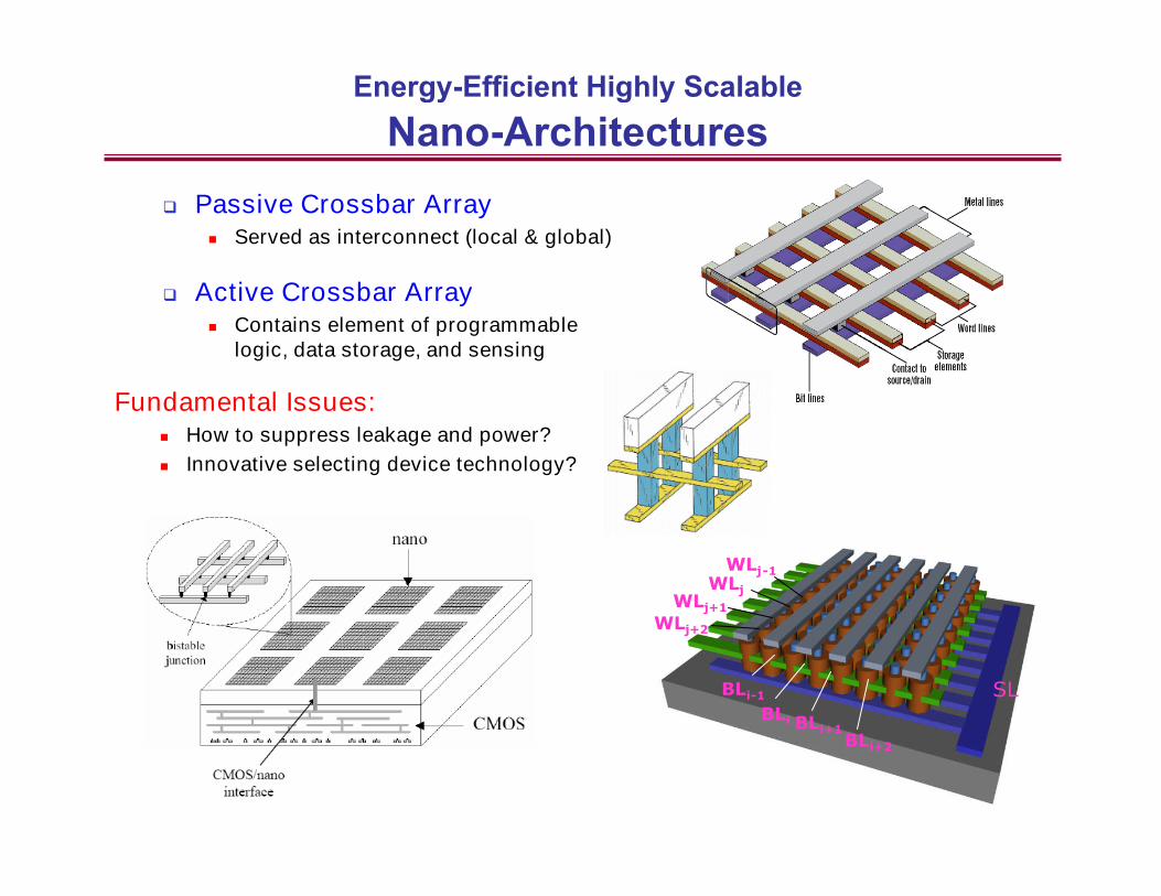
Fundamental Issues: How to suppress leakage and power? Innovative selecting device technology?
Passive Crossbar Array Served as interconnect (local & global)
Active Crossbar Array Contains element of programmable
logic, data storage, and sensing
SLBLi-1
BLi BLi+1BLi+2
WLj-1WLj
WLj+1WLj+2

Use of biomolecules asthe building elements in agroup of functionaldevices for informationdetection and processing
Communication betweenbiomolecules to nanoelectronics, e.g., Electron transfer Charge storage Biomolecules-
semiconductor interface Neuron-nanowire
interface
Bio-reaction
ElectronicDetection

Research will be focused on utilizing biomolecules as functional building elements todesign energy-efficient, bio-mimetic devices and circuits with functionality that
currently silicon-based chip technology is conducting.

Research Phase/Time Scale
1st generationSilicon-Based
2nd generationThin-Film-Based
3rd generationNano-Based
4th generationBiology-Based
Why Nanomaterials? High-conversion efficiency (surface-intensive structures) Tunable band-gap (wide spectrum light harvesting) Low-cost (thin film based) Possible materials: s-NWs, m-NWs, CNTs
Why Biomaterials? Bio-enabled solar cells utilizing biomolecules to
convert solar energy into chemical energy (similarto photosynthesis)
Bio-fuel cell use body fluids as a fuel for theelectrical powering of implantable devices