narrow band microstrip filter design with ni mwo · pdf filedaniel g. swanson, jr. dgs...
TRANSCRIPT

Daniel G. Swanson, Jr.DGS Associates, LLC
Boulder, CO
www.dgsboulder.com
Narrowband Microstrip Filter Design With NI AWR
Microwave Office
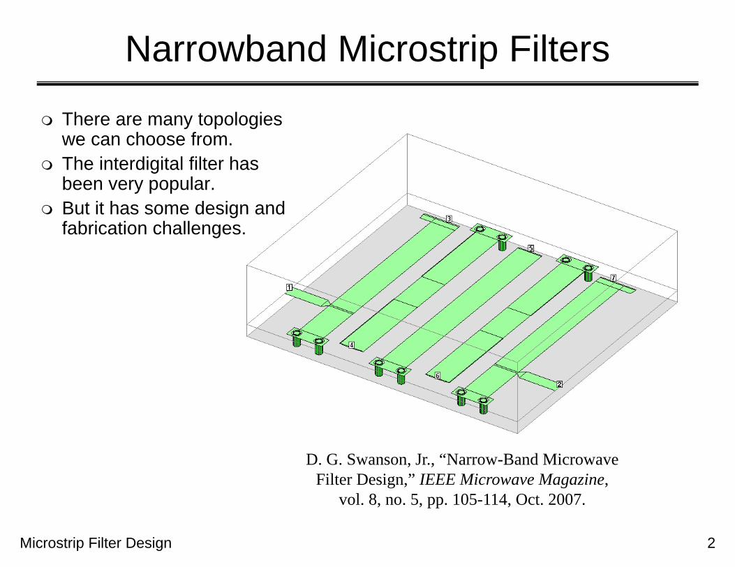
Narrowband Microstrip Filters
Microstrip Filter Design 2
D. G. Swanson, Jr., “Narrow-Band Microwave Filter Design,” IEEE Microwave Magazine,
vol. 8, no. 5, pp. 105-114, Oct. 2007.
There are many topologies we can choose from.
The interdigital filter has been very popular.
But it has some design and fabrication challenges.
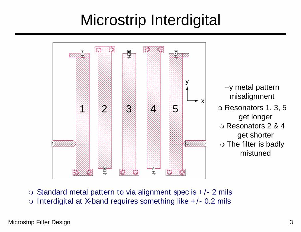
Microstrip Interdigital
Microstrip Filter Design 3
y
x1 2 3 4 5
Standard metal pattern to via alignment spec is +/- 2 mils Interdigital at X-band requires something like +/- 0.2 mils
+y metal pattern misalignment
Resonators 1, 3, 5 get longer
Resonators 2 & 4 get shorter
The filter is badly mistuned

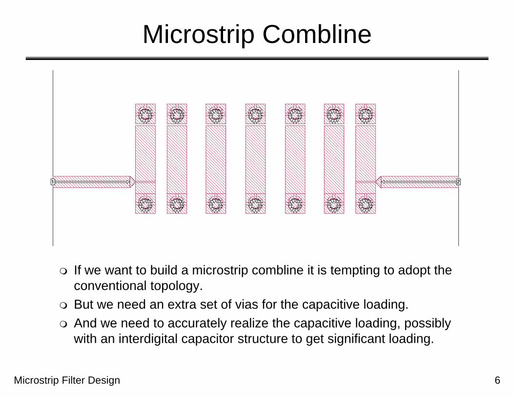
Microstrip Combline
Microstrip interdigital topology– Has been a workhorse for many years– Very compact in terms of wavelengths– Very sensitive to absolute via placement– Very sensitive to alignment of metal pattern to vias– Y-axis misalignment rapidly detunes filter
Microstrip combline topology– Has not been studied in detail– Also very compact in terms of wavelengths– True combline requires loading capacitors and extra vias– Microstrip combline is not pure TEM, allows longer resonator– All resonators are grounded at the same end– Y-axis misalignment should only shift center frequency
Microstrip Filter Design 4
Microstrip Filter Design 5
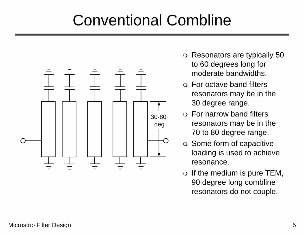
Conventional Combline
Resonators are typically 50 to 60 degrees long for moderate bandwidths.
For octave band filters resonators may be in the 30 degree range.
For narrow band filters resonators may be in the 70 to 80 degree range.
Some form of capacitive loading is used to achieve resonance.
If the medium is pure TEM, 90 degree long combline resonators do not couple.
30-80deg
Microstrip Filter Design 6
Microstrip Combline
If we want to build a microstrip combline it is tempting to adopt the conventional topology.
But we need an extra set of vias for the capacitive loading. And we need to accurately realize the capacitive loading, possibly
with an interdigital capacitor structure to get significant loading.

Microstrip Filter Design 7
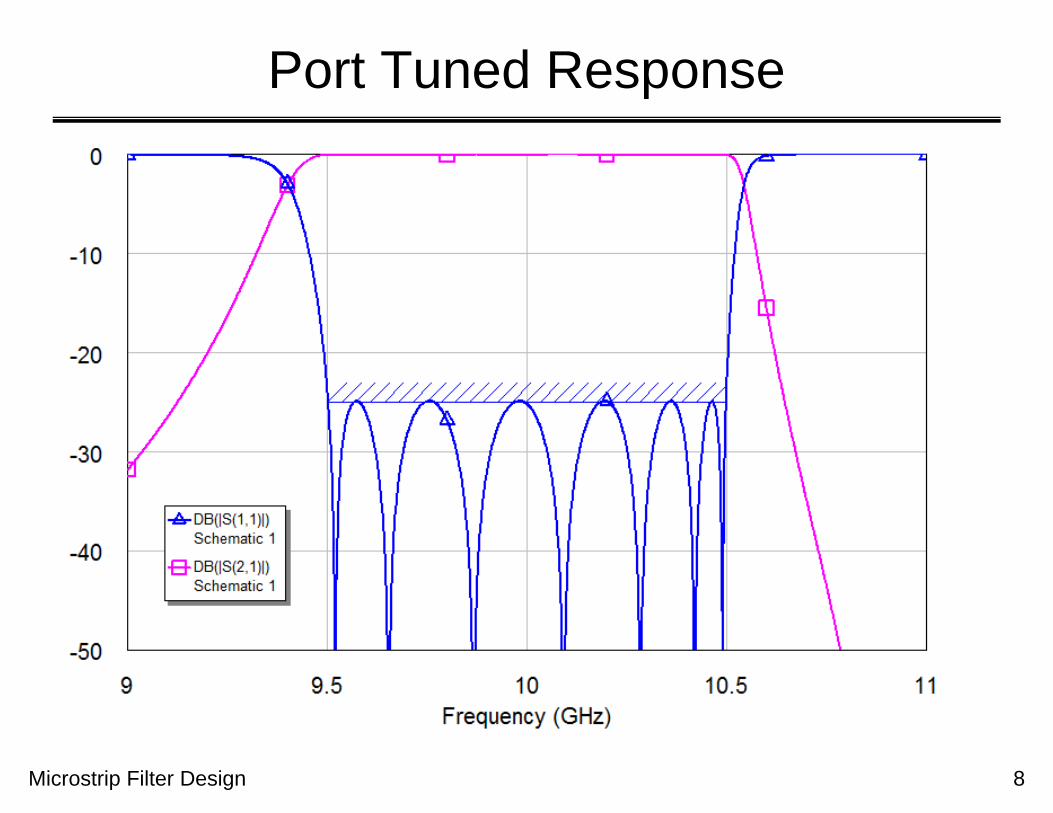
10% BW Microstrip Combline
What if we arbitrarily throw away the capacitive top loading? Our first assumption is that resonators will be close to 90 degrees
long and we may not get much coupling. This assumes the vias are ideal short circuits, which of course
they are not. It also assumes a pure TEM environment, which microstrip is not. In fact, we can port tune this structure to be a 10% bandwidth filter.
15 mil alumina25 mil wide resonatorsL = 94 mils
Microstrip Filter Design 8
Port Tuned Response

Microstrip Filter Design 9
10% BW Microstrip Combline
After optimization, the printed parts of the resonators are 73 to 77 degrees long, depending on the assumed reference plane for the vias.
We have some capacitive loading due to the open end fringing.
And we have significant loading due to the finite inductance of the vias.
There is also some mutual inductance between the vias.
Compared to the conventional approach, this microstrip combline is both bottom loaded and top loaded.
73-77deg
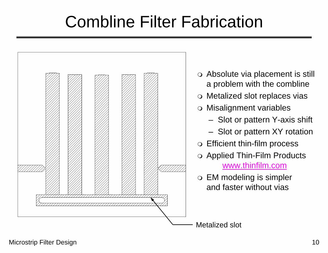
Combline Filter Fabrication
Microstrip Filter Design 10
Absolute via placement is still a problem with the combline
Metalized slot replaces vias Misalignment variables
– Slot or pattern Y-axis shift– Slot or pattern XY rotation
Efficient thin-film process Applied Thin-Film Products
www.thinfilm.com EM modeling is simpler
and faster without vias
Metalized slot
Microstrip Filter Design 11
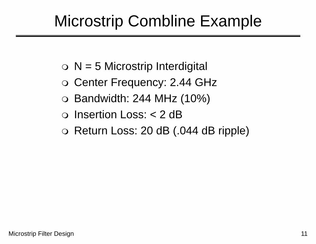
Microstrip Combline Example
N = 5 Microstrip Interdigital Center Frequency: 2.44 GHz Bandwidth: 244 MHz (10%) Insertion Loss: < 2 dB Return Loss: 20 dB (.044 dB ripple)

Microstrip Filter Design 12
Design Flow Estimate order of filter and stopband rejection Choose waveguide channel dimensions
– Distributed filters couple to the waveguide channel Build model of proposed resonator (with loss)
– Compute available Qu– Estimate insertion loss
Build Kij design curve (no loss) Build Qex design curve (no loss) Build model of complete filter and apply port tuning Use port tuning corrections to refine filter dimensions Do final run of filter with loss turned on
– Verify insertion loss in passband– Verify rejection in stopbands

Microstrip Filter Design 13
Chebyshev Lowpass Prototype
N is the lowpass or bandpass filter order. The gi’s are frequency and impedance scaled values for a
lowpass filter with a cutoff frequency of = 1 radian and a return loss of 20 dB.
Any given passband ripple / return loss level requires a unique table.
Other tables are available in the literature or the gi’s canbe computed.
Chebyshev Lowpass Prototype: 0.044 dB ripple, 20 dB return loss, 1.22 VSWRN g0 g1 g2 g3 g4 g5 g6 g7 g8 g9 g10 g1 - gN
2 1.0000 0.6682 0.5462 1.2222 1.2144
3 1.0000 0.8534 1.1039 0.8534 1.0000 2.8144
4 1.0000 0.9332 1.2923 1.5795 0.7636 1.2222 4.5727
5 1.0000 0.9732 1.3723 1.8032 1.3723 0.9732 1.0000 6.4989
6 1.0000 0.9958 1.4131 1.8950 1.5505 1.7272 0.8147 1.2222 8.4011
7 1.0000 1.0097 1.4368 1.9414 1.6216 1.9414 1.4368 1.0097 1.0000 10.4028
8 1.0000 1.0189 1.4518 1.9682 1.6570 2.0252 1.6104 1.7744 0.8336 1.2222 12.3447
9 1.0000 1.0252 1.4618 1.9852 1.6772 2.0662 1.6772 1.9852 1.4618 1.0252 1.0000 14.3710

Microstrip Qu
Microstrip Filter Design 14
25mil (.635mm) thick aluminaassumed r = 9.8
50mil by 435mil(1.27mm by 11.05mm)
Vertical via metal
EMSightAWRDE V11
150 mil
25 mil600 mil
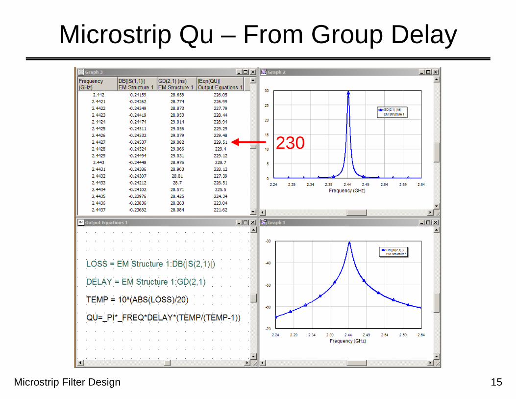
Microstrip Qu – From Group Delay
Microstrip Filter Design 15
230

Microstrip Filter Design 16
Midband Insertion LossChebyshev Lowpass Prototype: 0.044 dB ripple, 20 dB return loss, 1.22 VSWR
N g0 g1 g2 g3 g4 g5 g6 g7 g8 g9 g10 g1 - gN
2 1.0000 0.6682 0.5462 1.2222 1.2144
3 1.0000 0.8534 1.1039 0.8534 1.0000 2.8144
4 1.0000 0.9332 1.2923 1.5795 0.7636 1.2222 4.5727
5 1.0000 0.9732 1.3723 1.8032 1.3723 0.9732 1.0000 6.4989
6 1.0000 0.9958 1.4131 1.8950 1.5505 1.7272 0.8147 1.2222 8.4011
7 1.0000 1.0097 1.4368 1.9414 1.6216 1.9414 1.4368 1.0097 1.0000 10.4028
8 1.0000 1.0189 1.4518 1.9682 1.6570 2.0252 1.6104 1.7744 0.8336 1.2222 12.3447
9 1.0000 1.0252 1.4618 1.9852 1.6772 2.0662 1.6772 1.9852 1.4618 1.0252 1.0000 14.3710
dB 23.1230244.0
44.24989.6343.4
343.4)(
01
0
u
N
ii
Qf
fgfLoss
Loss will be higher at the band edges.

Microstrip Filter Design 17
Dishal’s Method
As early as 1951, Milton Dishal [2] recognized that any narrow band, lumped element or distributed bandpass filter could be described by three fundamental variables:– the synchronous tuning frequency, f0
– the couplings between adjacent resonators, Kr,r+1
– the singly loaded or external Q, Qex
The Kij set the bandwidth of the filter and the Qex sets thereturn loss level.
For any narrowband filter (<10% bandwidth) we can compute the required Kij and Qex from the Chebyshev lowpass prototype.
The K and Q concept is universal and can be applied to any lumped element or distributed filter topology or technology [4,5].

Microstrip Filter Design 18
Definition of Kij and Qex
0
12210
0
12
10
12
100
2
)(
fffBWfff
ggBW
ggfffK
BWgg
ffggfQ
jijiij
ex
f1 = bandpass filter lower equal ripple frequency
f2 = bandpass filter upper equal ripple frequency
f0 = bandpass filter center frequency
BW = percentage bandwidth
gi = prototype element value for element i
Note: Equations assume Qu is infinite.

Microstrip Filter Design 19
Our Filter: N = 5, BW = 10%
393.91.09393.00.1
0643.07691.13577.1
1.0
0882.03677.19393.0
1.0
10
323,2
212,1
BWggQ
ggBWK
ggBWK
ex
Chebyshev Lowpass Prototype: 0.044 dB ripple, 20 dB return loss, 1.22 VSWRN g0 g1 g2 g3 g4 g5 g6 g7 g8 g9 g10 g1 - gN
2 1.0000 0.6682 0.5462 1.2222 1.2144
3 1.0000 0.8534 1.1039 0.8534 1.0000 2.8144
4 1.0000 0.9332 1.2923 1.5795 0.7636 1.2222 4.5727
5 1.0000 0.9732 1.3723 1.8032 1.3723 0.9732 1.0000 6.4989
6 1.0000 0.9958 1.4131 1.8950 1.5505 1.7272 0.8147 1.2222 8.4011
7 1.0000 1.0097 1.4368 1.9414 1.6216 1.9414 1.4368 1.0097 1.0000 10.4028
8 1.0000 1.0189 1.4518 1.9682 1.6570 2.0252 1.6104 1.7744 0.8336 1.2222 12.3447
9 1.0000 1.0252 1.4618 1.9852 1.6772 2.0662 1.6772 1.9852 1.4618 1.0252 1.0000 14.3710
Microstrip Filter Design 20
Computing Spacings and Tap Height
Our resonator geometry is now fixed. We have enough Qu to meet the insertion loss goal. We have goals for the Kij’s and Qex Now we need to compute the spacings between
resonators and the tap height.
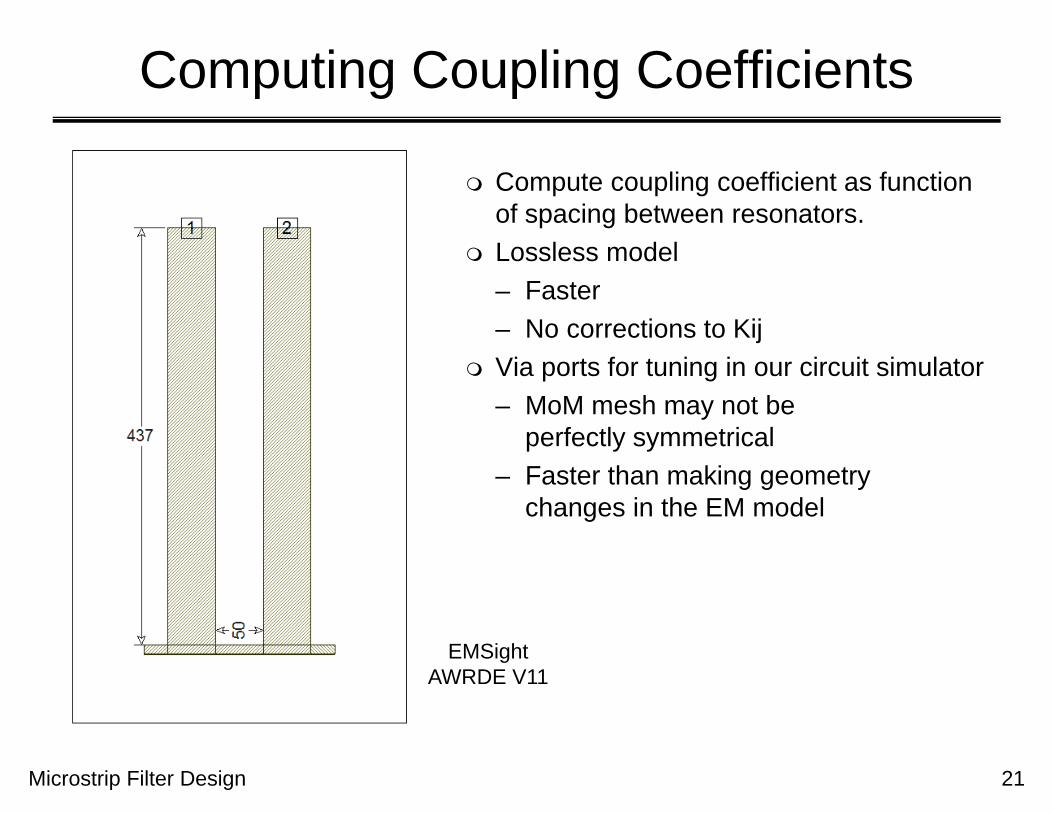
Computing Coupling Coefficients
Microstrip Filter Design 21
Compute coupling coefficient as function of spacing between resonators.
Lossless model– Faster– No corrections to Kij
Via ports for tuning in our circuit simulator– MoM mesh may not be
perfectly symmetrical– Faster than making geometry
changes in the EM model
EMSightAWRDE V11
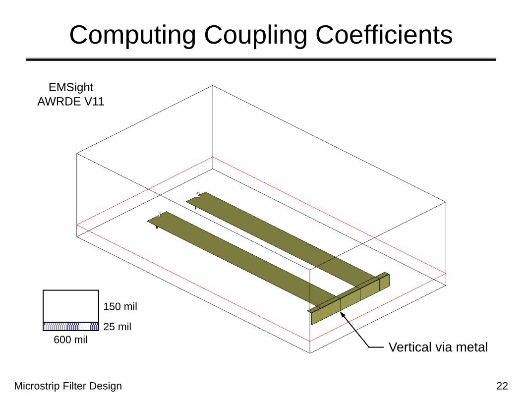
Computing Coupling Coefficients
Microstrip Filter Design 22
150 mil
25 mil600 mil
EMSightAWRDE V11
Vertical via metal

Extracting Coupling Coefficients
Microstrip Filter Design 23
0)))2,2(((0)))1,1(((
YimmagYimmag
We want to force synchronous tuning.
At resonance:
Loosely couplewith transformers.

Extracting Coupling Coefficients
Microstrip Filter Design 24
-30 dB min
MHz 148Bandwidth Coupling
0607.0tCoefficien Coupling
12
0
12
fff
ff

Coupling Curve: Fit in Mathcad
Microstrip Filter Design 25
29600.32903.11137.0 KKSpacing 150 mil
25 mil600 mil

Computing Qex
Microstrip Filter Design 26
Tune to center frequency at Port 2. Measure reflected group delay at Port 1. Tap height sets the return loss level
of our filter. Note this resonator is longer than the
resonators used to compute couplings.

Port Tuned Reflected Delay
Microstrip Filter Design 27
98.92
605.244.21416.34
)nS()GHz(2
ex
dex
Q
tfQ Tap_Height = 93 mils

Qex Curve: Fit in Mathcad
Microstrip Filter Design 28
2410498.40158.02012.0 DelayDelayHeight Tap 150 mil
25 mil600 mil

First Iteration Geometry
Microstrip Filter Design 29
S1 = 31 milsS2 = 47 mils
L1 = 442 milsL2 = 437 mils
Tap Height = 97 mils

Default Meshing
Microstrip Filter Design 30
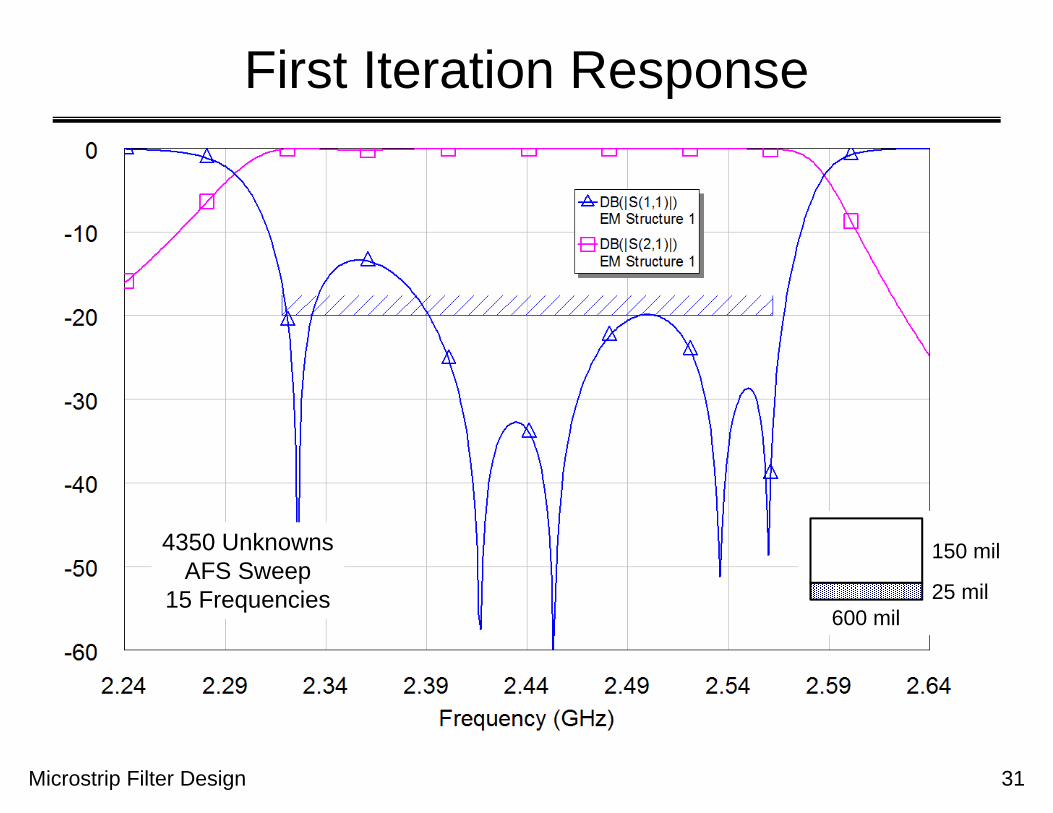
First Iteration Response
Microstrip Filter Design 31
4350 UnknownsAFS Sweep
15 Frequencies
150 mil
25 mil600 mil
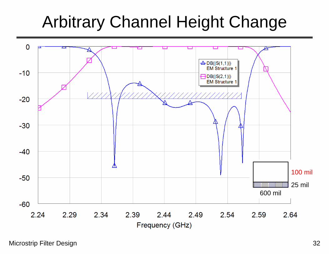
Arbitrary Channel Height Change
Microstrip Filter Design 32
100 mil
25 mil600 mil

Internal Ports for Port Tuning
Microstrip Filter Design 33
Internal nodes
External port
Tuning element
Low error Very effective for
frequency tuning Limited to lumped
elements by the transformer
How do we tune couplings?

Impact of Internal Ports
Microstrip Filter Design 34

Port Tuning With Internal Ports
Microstrip Filter Design 35
110
ij
i
jiijij
KL
LLKM
Add negative offset inductors so coupled L’s don’t go negative.
Coupled inductor array
Dummy element
“zero tuning” = +20 pH
Mutual couplings
Mutual couplingstune EM circuit couplings
Custom symbol

Port Tuning with EQR_OPT
Microstrip Filter Design 36
General purpose optimizers may work fine for low order filters, but they can be inefficient for more complex filters.
EQR_OPT_MWO is a dedicated optimizer for microwave filters.
It finds an exact equal ripple response with a very small number of iterations.
It communicates with Microwave Office via the COM interface.
It works on any Chebyshev filter thatcan be defined in Microwave Office.
We can also use it to port tunean S-parameter file from anyEM simulator.www.swfilterdesign.com

Second Iteration: Port Tuned
Microstrip Filter Design 37
X X X X X
X EM simulation frequencies

What Do The Tunings Tell Us?
Microstrip Filter Design 38
Center resonator tuning is almost perfect(remember “zero” is +20 pH)
The outer resonators want to be longer The first and last gaps want to be smaller The inner gaps want to be larger Return loss tells us the tap position wants
to move down very slightly The resonator and coupling tunings
will interact The general strategy is to go after the
largest errors at each step
Next step: Resonators 1, 2, 4, 5 each one mil longerMove tap down one mil
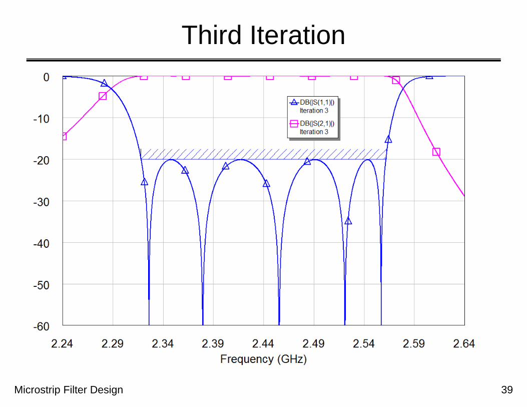
Third Iteration
Microstrip Filter Design 39
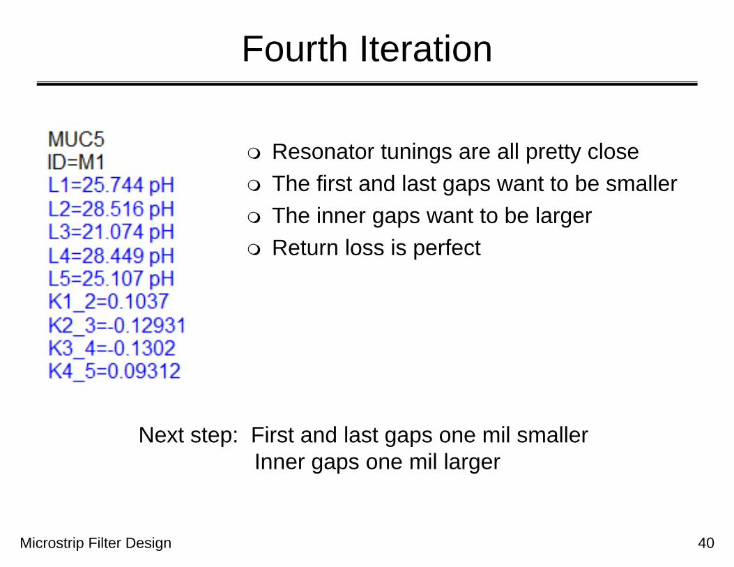
Fourth Iteration
Microstrip Filter Design 40
Resonator tunings are all pretty close The first and last gaps want to be smaller The inner gaps want to be larger Return loss is perfect
Next step: First and last gaps one mil smallerInner gaps one mil larger

Fifth Iteration
Microstrip Filter Design 41
Coupling corrections are small and in the numerical noise (note opposite signs)
Resonator tunings have shifted We need less than a full one mil change
in resonator length and resonator spacing.
Next step: Fine tune open endsFine tune couplings

Fine Tunings
Microstrip Filter Design 42
Add and subtract bits of metal at the open ends to fine tune the resonators.
Adding or subtracting metal at the base of the resonators fine tunes the coupling.
Reso 1 Reso 2 Reso 3
We have to go back and forth a little between
frequency and coupling adjustments.

Final Tuning
Microstrip Filter Design 43
If we set the tunings to zero and see very little movement in the response we are done.
Next step is to remove the tuning ports and do a twoport analysis of the filter.
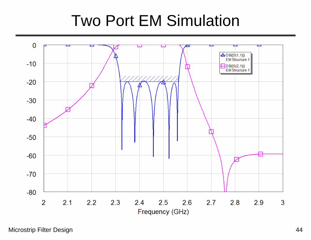
Two Port EM Simulation
Microstrip Filter Design 44
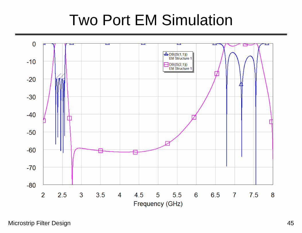
Two Port EM Simulation
Microstrip Filter Design 45

Summary
Dishal’s K and Q method leads us to a simple design flowfor narrowband filters.
We can modernize the method by using EMSight to buildthe Kij and Qex design curves that we need.
We can then build a complete model of our filter in EMSight, port tune it and get a very good prediction of performance.
These virtual prototypes in our EM simulator avoid thetime and expense of multiple hardware prototypes.
Experience has shown that we can rely on theEM simulator models.
Microstrip Filter Design 46

Microstrip Filter Design 48
References
[1] R. Levy, R. Snyder and G. Matthaei, “Design of Microwave Filters,” IEEE Trans. Microwave Theory Tech., vol. MTT-50, pp. 783-793, March 2002.
[2] M. Dishal, “Alignment and adjustment of synchronously tuned multiple resonate circuit filters,” Proc IRE, vol. 30, pp. 1448-1455, Nov. 1951.
[3] M. Dishal, “A simple design procedure for small percentage bandwidth round-rod interdigital filters, IEEE Trans. Microwave Theory Tech., vol. MTT-13, pp. 696-698, Sept. 1965.
[4] J. Wong, “Microstrip tapped-line filter design,” IEEE Trans. Microwave Theory Tech., vol. MTT-27, pp. 44-50, Jan. 1979.
[5] D. G. Swanson, Jr., “Narrow-Band Microwave Filter Design,” IEEE Microwave Magazine, vol. 8, no. 5, pp. 105-114, Oct. 2007.
[6] D. G. Swanson, Jr., “Corrections to “Narrow-Band Microwave Filter Design, “ IEEE Microwave Magazine, vol. 9, no. 1, p. 116, Feb. 2008.