nasa contribu-ons to the x-ifu contribu-ons to the x-ifu simon bandler - tes microcalorimeter...
TRANSCRIPT

NASAContribu-onstotheX-IFUSimonBandler- TESmicrocalorimeterprojectmanager- onbehalfoftheteamdevelopingX-IFUmicrocalorimeterarrays
• Consor'ummembership• DMArraydevelopment• Arrayfabrica'onprocessing
development• StudiesofTESsunderACbias• X-IFUarrayconfigura'ontrade• X-IFUscalearraytestplaDormbuild-up• Mul'plexingdevelopments
• Updatedscheduledetails

NowformallypartoftheX-IFU“Proto-consor-um”
• RichardKelley:MemberoftheX-IFUconsor@umboard• SimonBandler:TESmicrocalorimeterprojectmanager• CarolineKilbourne:[email protected],S.Bandler&C.KilbourneaMendedthethirdX-IFUconsor'ummee'ng(10/26-10/28),includingthefollowingsplintermee'ngs:
• Consor'umboardmee'ng(RK)• Na'onalprojectmanagermee'ng(SB)• Sensorarrayconfigura'onmee'ng(SB,CK&RK)• Informalapertureassemblymee'ng(CK&RK)

Demonstration model (DM) kilo-pixel arrays - being fabricated and tested • 32x32array–close-packedmicrostripwiring• Absorbers:Au:1.5µm,Bi:3.0µm,on250µmpitch
UniformityofTc/performanceisimproving-con'nuedstudiesoftransi'onproper'es,heatcapacity&noise

Developingmicrofabrica-ontechniquesforfabrica-ng“hybrid”arrays
Central5x5arrayoffree-standingabsorbers:all-Auona50µmpitch,4.0µmthick.Surroundinglargeabsorbers:AuBiona250µmpitch,2.5µmAu,3µmBi.
Photograph&SEMimageoftwotypesofabsorbersfabricatedonsingleSisubstrate

TESsunderACbias• NewdetectorsenttoSRONforACbiastestsa`erextensivecharacteriza'onatGSFC.• Purpose:tostudydifferentgeometricconfigura'onunderACbias
• Differentpixelsizes:50μm,100μm,120μm,140μm.• Differentstemcontactgeometries.• Micro-stripwiring.
• StephenSmithfromGSFCvisitedSRONfor2weekstopar'cipateintes'ng/datainterpreta'onandlearnACmeasurementtechniques.
• GSFCbuildingupdedicatedACbiasread-outcapability,supportedbySRON.• ElectronicsandresonatorcomponentsbeingkindlyprovidedbySRON,SQUIDsbyVTT.

X-IFUsensorarrayconfigura-ontrade
Mo'va'on:
•AthenaL2proposal:"uniform"sensorarraywithequalperformance(sensi'vity,count-rate)overa5'FoV(goal=7').
- realizingallrequirementsinuniformarrayischallenging- achievingoneormoregoalsisunrealis'c.- configura'onunnecessarilyrequirespoint-source-drivencount-raterequirementsmet
inallpixels.
•PastdevelopmentatGSFCofarangeofTESpixelgeometriesincludesarrayscombiningmul'plepixeltypes.
=>X-IFUcouldbenefitfromaconfigura'onthatcombines: -asub-arrayofpixelsop'mizedfor(bright)point-sources -mainarrayop'mizedforalargerfieldofview.
•Athenasciencestudyteamreviewedthescienceandperformedseriesofsimula'onstoevaluatethescienceimplica'onsof"hybrid"sensorarray.
-concludedthathybridarrayofferssignificantimprovementinX-IFUsciencecapabili'escomparedtouniformarray•Inparallel,areviewoftheimplementa'onaspectsofthesensorarrayisalsoneeded.

Study'meline: July-Oct.:firstdra`sofchapters3-7 Oct.28:presenta'ons&discussionsinconsor'umsplintermee'ng Nov..:review&updates,submittoX-IFUmanagementteam
Version1.0ofdocumentjustissuedandsubmiMedtoX-IFUmanagementteam.
Versionincludes:-summaryofrelatedsciencegoalsandrequirements-2(key)chaptersfromGSFCaboutthesensorarrayconfigura'onsandimplementa'onissues-summaryonimpactontheenergyresolu'onbudgetoftheSPApixels-conclusionsoftheimpactonthereadoutelectronics-summaryofthe"otherimplementa'onissues”discussedatsplintermee'ng-preliminaryconclusionsandrecommenda'ons
Didier BarretTES array optimization
CDF baseline
Didier BarretTES array optimization
Hybrid array - 5’ field of view

overall sketch: 960 pixel concept
960 pix. TDM/CDM: Doriese, 10/20/2015 2
some features/data: • 40-row architecture • 6 side panels • interface/mux “chip”: 17mm X 30mm
• 2 col X 40 row • for now, mux chips cemented on • eventually mux & int. integrated
• ID of 50 mK shield as small as 4.368” • height presently 2.73” • hexagonal TES chip is 91mm on diagonal
and fits in present NASA 100mm DRIE • PCBs all small and modular to aid rapid
redesign (if needed) Not yet chosen whether round-the-corner technology will be some kind of flex or ceramic with 45o beveled edges.
Somefeatures:• 40-rowarchitecture• 24Columns(4/side)
=>960pixelcharacteriza'on• 6sidepanels• Heat-sinkingtorearsideofarray
waferavailableviaribbon/wire-bonds
• Kinema'cmoun'ngofwafers• HexagonalTESchipis91mmon
diagonal
Architectureforkilo-pixelscalecharacteriza-onofarrayswith3840TESs

TES wafer
960 pix. TDM/CDM: Doriese, 10/20/2015 11
Converging on a TDM/FDM solution:
• sectors 1, 3, 5 have interior reserved for FDM pickup coils
• sectors 2, 4, 6 contain: • TDM wiring streets • KM slots (rot. by 2o about ctr.) • possibly a hole to allow front-
side Au HS bonds • press points for support of
backside Au HS bonds
• still TBD: • locations of glue spots for
flexures to mount into SRON module.
• whether FDM will require a variant in which 1, 3, 5 have no (TDM) edge bondpads
Working,towardswafersize,shape&layoutforfuturekilo-pixelleveltes'ngofX-IFUstylearrays,via:• Wire-bonding&DC-biasedtes'ng• CoilcouplingandAC-biasedtestsConvergingonsolu'onwith:• DC-biasedpixelsinsectors1,3,5,• AC-biasedpixelswithtransformer
coilsinsectors2,4,6S'llTBD:• Loca'onsofgluespotsforflexures
tomountintoSRONmodule.• Removalofbond-padsinsectors1,3,5
TESarraywaferlayoutforkilo-pixelleveltes-ng/demonstra-ons

Wire-rou-ngdevelopment:towards3840TESsPreliminarywire-rou'ngwithinthe3840pixelTESarray.
Fullhexagonalarraywith3840squarepixelsonasquaregrid.
• Expandedviewofoneregionwithhighestwire.• Wiringon"mun'ns"betweenpixels,between
TES“keep-out”areas• Currently:Maximum17micros'pwiresbetween
pixelsonamun'n,&32alongdiagonal• Versionofwiringwith“hybrid”array“Op'on-2”
wiringnowworkedoutinprinciple–masksjuststar'ngtobedrawn

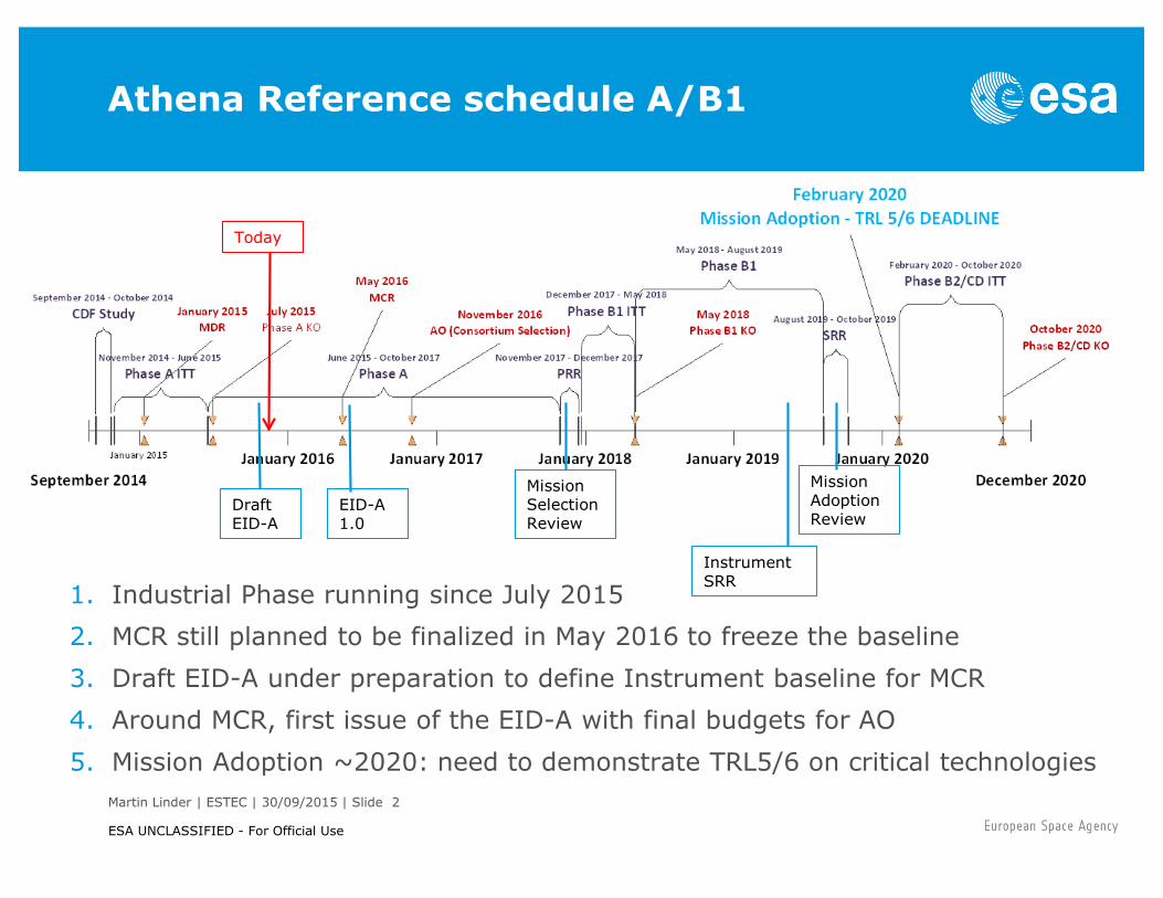
Athena +m i s s ion +<me l ine • Phase A: 2015-2017 • Phase A1 industry study kickoffs (parallel contracts) – August 2015 • Mission Concept Review (MCR) data package (2 configurations) - March
2016 • MCR completed - May 2016
• Agreements for non-ESA contributions in place
• Mission baseline selection - June 2016 • Phase A2 kickoff - June 2016 • AO for science instruments - July 2016 • Selection of instrument consortia - November 2016 • Preliminary Requirements Review (PRR) data package - November 2017 • PRR completed (end phase A) - December 2017
• Phase B1: 2018-2019 • Technology developments (mirror, detectors) at TRL > 5-6 - 2019 • System Requirements Review - End 2019 • Mission adoption by the ESA Science Program Committee - Feb 2020
• Phase B2/C/D kickoff - Nov 2020 • Launch - 2028
Martin Linder | ESTEC | 30/09/2015 | Slide 2
ESA UNCLASSIFIED - For Official Use
Athena Reference schedule A/B1
1. Industrial Phase running since July 2015 2. MCR still planned to be finalized in May 2016 to freeze the baseline 3. Draft EID-A under preparation to define Instrument baseline for MCR 4. Around MCR, first issue of the EID-A with final budgets for AO 5. Mission Adoption ~2020: need to demonstrate TRL5/6 on critical technologies
Draft EID-A
EID-A 1.0
Today
Mission Selection Review
Mission AdoptionReview
Instrument SRR
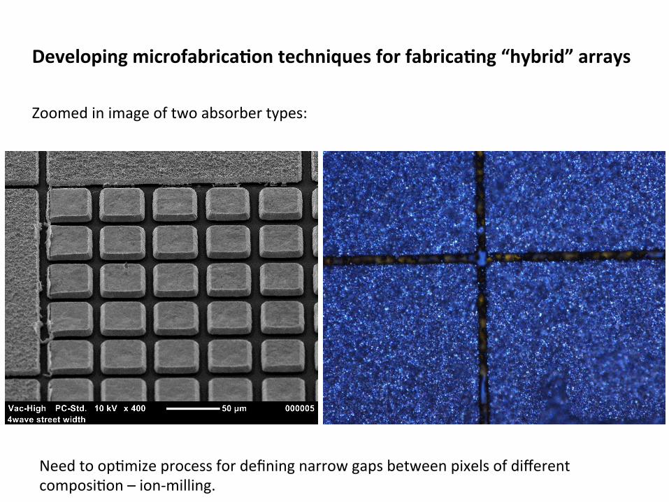
Developingmicrofabrica-ontechniquesforfabrica-ng“hybrid”arrays
Zoomedinimageoftwoabsorbertypes:
Needtoop'mizeprocessfordefiningnarrowgapsbetweenpixelsofdifferentcomposi'on–ion-milling.
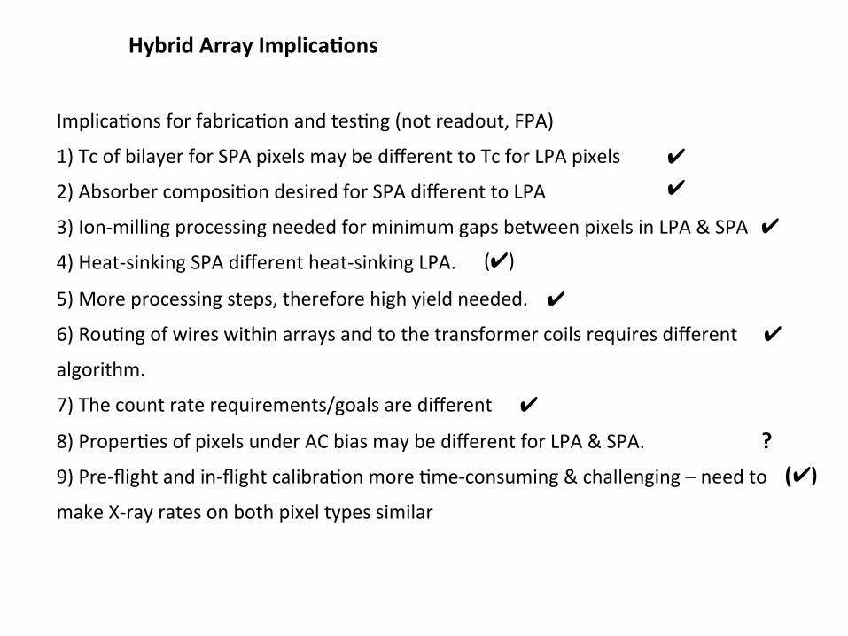
Implica'onsforfabrica'onandtes'ng(notreadout,FPA)
1)TcofbilayerforSPApixelsmaybedifferenttoTcforLPApixels
2)Absorbercomposi'ondesiredforSPAdifferenttoLPA
3)Ion-millingprocessingneededforminimumgapsbetweenpixelsinLPA&SPA
4)Heat-sinkingSPAdifferentheat-sinkingLPA.
5)Moreprocessingsteps,thereforehighyieldneeded.
6)Rou'ngofwireswithinarraysandtothetransformercoilsrequiresdifferent
algorithm.
7)Thecountraterequirements/goalsaredifferent
8)Proper'esofpixelsunderACbiasmaybedifferentforLPA&SPA.
9)Pre-flightandin-flightcalibra'onmore'me-consuming&challenging–needto
makeX-rayratesonbothpixeltypessimilar
HybridArrayImplica-ons
✔✔
✔
(✔)
✔
✔
✔
?(✔)

Programma-candpersonneldevelopments:
• CNEShasanewmanagementteamandanewprogramschedule(seelaterslides).- Wenowhave6addi'onalmonthsbeforethedeliveryofthemicrocalorimetersforthe
X-IFUdevelopmentmodel(DM)(Dec.2016).- ThereisnolongeraneedforcalorimetersforanengineeringmodelJune2017.This
hasbeenreplacedwiththeneedforacalorimeterarrayforthe“DM-2”FPA,nowDec.2017,essen'allyiden'calwhatwaspreviouslybeingdevelopedfortheEM.
- Thesechangeshavealmostnoeffectonourresearchprogram,asdeliverablesares'llessen'allythesame,andpreviousschedulewasextremelyaggressive.

Otherdevelopmentac-vi-estakingplace:• TDMmul'plexing(3x32)demonstra'onsystem(Lisa)evolvedtoallowobserveX-raythroughside-window.
-SystemwillshiptoEBITinearly2016.• NewTDMmul'plexingdemonstra'onbeingbuiltandassembled
-twonewheat-switchtypesbeingdeveloped-newsaltpillbeingbuilt-focalplaneassembly“snout”iden'caltooneinLisabeingpurchased-newplanarfocalplaneassemblyalsobeingdeveloped
• High-speedTDMelectronicsdevelopedatNIST,butneedsfurthermodifica'onstoimprovestabilityforuseatGSFC• FlightTDMelectronics/firmwareunderdevelopmentatGSFC• Instrumentcontrolanddataacquisi'onso`warecon'nuestoevolve
W.B. Doriese LTD-16 (Grenoble, France) Tuesday, 21 July, 2015intro: TDM & CDM TDM: old & new CDM-32
highly mature… but could work betterIn present 8-column x 30-row X-ray systems, ΔE ~ 4.5 eV. Why?
• SQUID noise = 0.4 µΦ0 / √Hz, when aliased, matters
• trow = 320 ns Æ arrival time within tfr ~10 µs frame matters.