national radio astronomy observatory mechanical
TRANSCRIPT

NATIONAL RADIO ASTRONOMY OBSERVATORYGREEN BANK, WEST VIRGINIA
ELECTRONICS DIVISION INTERNAL REPORT No, 173
MECHANICAL STABILITY OF DIODES FOR
CRYOGENIC 80-120 GHZ MIXER
RICHARD DECKER
NOVEMBER 1976
NUMBER OF COPIES: 150

GaAs CHIP CHOKE
WHISKER CHOKE (.006"QUARTZ)
CHIP
INTRODUCTION
Schottky barrier GaAs diodes are assembled with quartz microstrip r.f. chokes onto
a quartz substrate for operation in the cryogenic 80-120 GHz mixer. These diodes
exhibit finite operational life with the dominant failure mode being open circuit and
the secondary mode being degradation from whisker punch through. The past seven weeks
have been spent assembling replacement diodes for use in Tucson. Emphasis has been
on obtaining units that will cool without failing and will demonstrate good noise
performance. During this period, all phases of diode assembly and mounting have
been reviewed and several factors crucial to mechanical stability under cryogenic
operation have been illuminated. This memorandum documents and updates diode
construction, materials, and assembly procedures related to achievement of stability
and reliability.
1.0 Diode-Choke Subassembly
The GaAs Schottky barrier diode is mounted and contacted in the choke
subassembly shown in Figure 1.
.006" QUARTZSUBSTRATE
Figure 1. Diode-Choke Subassembly
The quartz chokes and substrates are 6 mils thick by 16.5 mils wide. The substrate
is 230 mils long and the individual chokes are each 125 mils long. Gold ribbon is
first ultrasonically bonded to the choke end sections and folded over the end to
provide a surface for electrical contact. The GaAs chip is soft soldered directly to
the inner (low impedance) end (folded over gold ribbon) of one choke.
1

ELECTRICAL CONTACT
MICROSCOPE
CHIP WHISKER CHOKE
SUBSTRATE
MICROMETER(PUSHER)
A 10 mil long phosphor bronze contact whisker 0.5 mil in diameter is
ultrasonically bonded to the inner end of the other choke on the top surface of
the gold ribbon (the gold is not folded over the ends of the whisker choke). The
whisker is fabricated of annealed phosphor bronze wire which has been electrolytically
pointed on one end and gold plated but is not bent to its final configuration prior to
mounting on the choke end. After the whisker is ultrasonically bonded, the bond is
soldered over to provide additional mechanical strength.
The whisker is bent to final form by hand using a scalpel blade and simple
alignment jig. The bending is such that the whisker goes down leaving the choke end,
then up forming a vee, and finally back level pointing directly away from the choke
end at the level of the (upper) choke surface.
The choke with diode chip attached is aligned and firmly bonded to the
quartz substrate using Eastman 910 contact cement. The back section of the choke
overhangs the substrate by 10 to 12 mils for subsequent proper alignment of the diode
in the waveguide section. A special fixture is used for "whiskering" (contacting) the
diode. The substrate with chip-choke is mounted in the fixture as shown in Figure 2.
LIGHT
Figure 2. Whisker Contacting Apparatus
2

TRANSFORMER BLOCKINDIUM LAND
DIODE-CHOKE SUBASSEMBLY
I.F.OUTPUT
11SP.5;1141
BELLOWS
BACKSHORTBLOCK
Electrical contact is maintained to both choke sections during the con-
tacting operation. Progress is monitored visually via the microscope and electricallyby a curve tracer connected across the chokes. Once the whisker contacts a Schottky
dot the diode forward characteristic may be observed on the curve tracer for
determination of q and Rs . If the diode is satisfactory, an additional whisker
deflection of 1.5 pm is inserted at the micrometer and a drop of Eastman 910 is
touched to the interface between the choke and substrate where surface tension causes
this to wet the entire interface and effect a strong bond. The diode-choke subassemblyis subsequently removed from the whiskering jig and is complete and available forfurther testing in a mixer block.
2.0 Diode-Mixer Block Assembly
The diode-choke subassembly is mounted in a channel in the mixer block in
such a manner that the chip and whisker are located across the waveguide. The sub-assembly is constrained in position by an opposing indium land and bellows in one
direction and by a spacer and bellows in the other direction as shown in Figure 3.
WAVEGUI DE APERTURE
Figure 3. Diode-Choke Subassembly Mountedin Mixer Block
There is no provision for constraint in the third direction other than the lateral
clearance of the choke subassembly in the channel in the mixer block which is about
1 mil on either side.
3

Two similar but different assembly techniques have been followed historicallyfor placing and mounting the diode-choke subassembly in the mixer block. In the
first technique, the choke subassembly is laid into the backshort block with thebellows retracted to the flush position. Then the i.f. connector is tightenedcompressing the i.f. bellows against the end of the choke. Finally the transformerblock is brought into position and tightened and the backshort side bellows istightened to hold the whisker side choke in contact with the built-up indium land.This assembly procedure has the disadvantage that the choke assembly is deflectedby the final bellows tightening and that the i.f. end of the choke is not centrally
aligned within the channel. The deflection tends to bend the quartz in a direction
that reduces whisker deflection.The second assembly procedure also starts with the choke subassembly in
position in the backshort block with the bellows retracted. However, the transformer
block is immediately clamped into position and the block is upended so that the i.f.end of the choke is visible through a binocular microscope. The bellows is tightenedgradually until the end of the choke subassembly is observed to move away from thebackshort block. The bellows is then given a final deflection of 1/2 to 3/4 turnwhich is about 12 to 18 mils (@ 25 mils/turn) of which 3 to 4 mils is free travelto bring the upper surface of the choke into contact with the indium land (whichmust be rolled flat beforehand). A disadvantage of the second assembly procedure
is that the choke subassembly is unsupported mechanically over the distance betweenthe indium land and the i.f. bellows contact.
3.0 Deflections, Constraints and Cryo enic Coolability
Problems of diode open circuits have arisen both before and after assemblyinto the mixer block and both before and after cooling to 77°K. In general, however,
the most difficult portion of the task is to get the diode to cool to 77°K withoutopening once mounted in the block. Several areas of importance that were uncovered
during attempts to fabricate and mount diodes that cooled successfully will be discussed.
3.1 Bad Whiskers or Bad Glue?
Two potential problem areas that arose early in the study and weresubsequently eliminated were bad whiskers and bad glue. A bad whisker is one which
distorts drastically upon cooling. It is apparently possible to make very badwhiskers using unannealed wire. We confirmed the fact that the whiskers being usedwere OK by fabricating a new batch using wire that was definitely annealed withoutany detectable improvement in the statistics of fabricating diodes that would cool.
4
Bad glue would be Eastman 910 that would not set up hard due to age and
would subsequently slip or flow under the shear stress and thus alter the critical
alignment and deflection between whisker and chip. We changed glue lots withoutnoticeable improvement in the situation. It is important to store the Eastman 910under refrigeration and to verify the bond quality if in doubt.
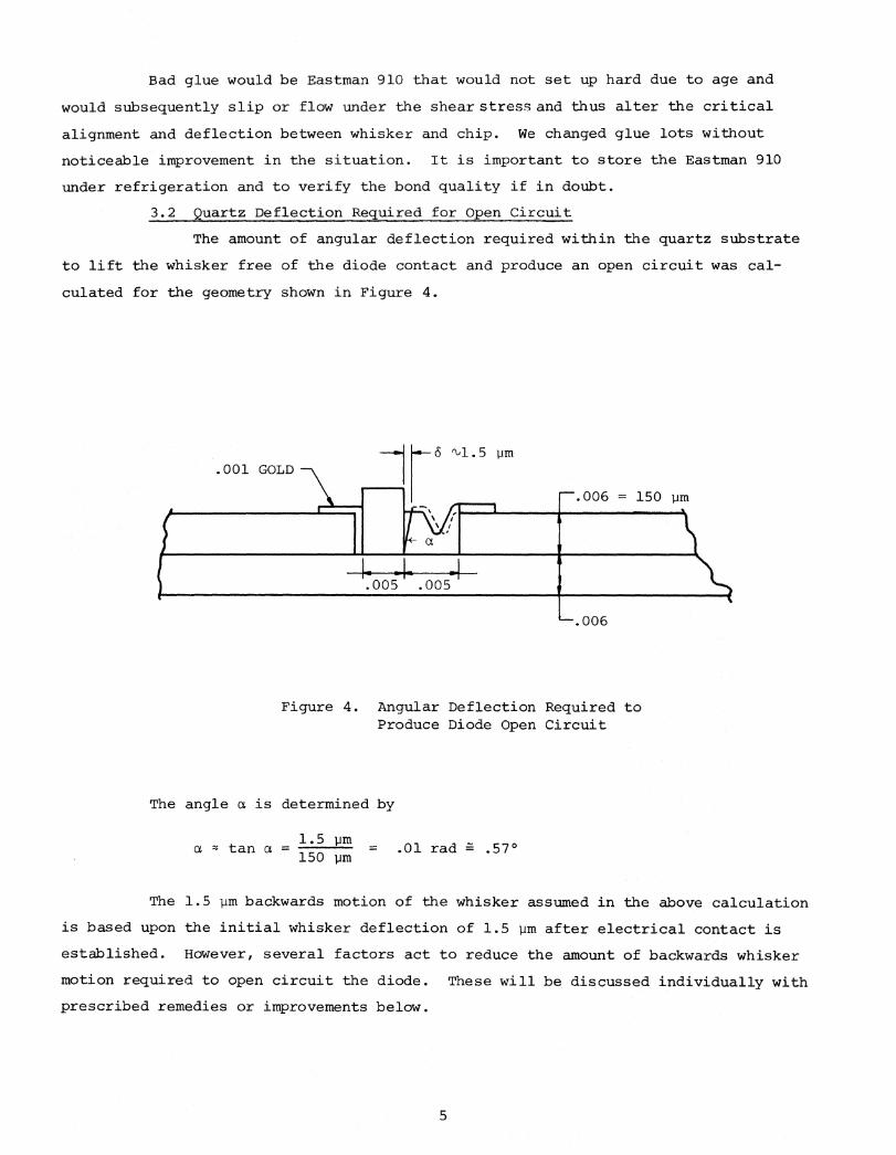
3.2 Quartz Deflection Required for Open Circuit The amount of angular deflection required within the quartz substrate
to lift the whisker free of the diode contact and produce an open circuit was cal-
culated for the geometry shown in Figure 4.
(b1.5 pm.001 GOLD
—.006
Figure 4. Angular Deflection Required toProduce Diode Open Circuit
The angle a is determined by
a tan a = 1.5 pm150 pm
.01 rad .57°,==.1
The 1.5 pm backwards motion of the whisker assumed in the above calculationis based upon the initial whisker deflection of 1.5 pm after electrical contact isestablished. However, several factors act to reduce the amount of backwards whiskermotion required to open circuit the diode. These will be discussed individually withprescribed remedies or improvements below.
5

3.3 Substrate Flexure in the Whiskering JigCurvature of the quartz substrate in the whiskering jig contributed
an error to the initial amount of whisker deflection. Pressure is applied to thetop surface of the whisker choke shown in Figure 2 during the whisker contactingprocess in order to establish electrical contact and to hold the choke in goodmechanical contact with the substrate. A vertical deflection in the center of thesubstrate of .001" (25.4 pm) corresponds to an angular deflection of about 8.7 x 10⁻³rad or an error of whisker deflection of about 1.3 pm. Obviously the substrate de-
flection in the whiskering jig must be kept well below this value. The present jig
has been improved in this area but would need a complete redesign to effectivelyeliminate the slight backing off of the whisker which occurs when the diode is removed
from the jig. A visual estimate of vertical deflection with the present jig is 2.5
to 5 pm which produces 0.13 to 0.26 pm of whisker "back up". This effect isparticularly pernicious since we must avoid overdeflection to prevent punch through
and whisker spreading.
3.4 Differential Contraction U on Cryogenic Cooling
Differential thermal contraction between the quartz substrate and theelements comprising the diode contacting structure will modify the whisker deflectionat cryogenic temperatures. The geometry is as shown in Figure 4. The thermal
expansion or contraction is expressed as
6Z = K A T = K A T
For cooling from room temperature (300°K) to 15°K we have AT = 285°K and obtain the
contractions given in Table 1.
Table 1 - Thermal Contraction of Diode Contact
MATERIAL t(pm1 K(x 10-6
°C-1
)69,(pm)
Quartz 279.4 .256 .0204Gold 35.4 13.2 .0956GaAs 127.0 6.0 .2172Phos. bronze 127.0 18.9 .6841
The net differential contraction obtained by substacting the contraction of thequartz from the sum of contractions of the gold, GaAs, and phosphor bronze is 0.98 pm.
6

nooGOLD
S.0l000 R 2
GaAs CRYSTAL
Figure 5. Plastically Deformed Whisker Tip
7
S.02
PHOSPHOR BRONZE WHISKER TIP
When added to the small whisker retraction resulting from deflection in the whiskering
jig, the total whisker retraction is between 1.11 pm and 1.24 pm. Since we only
started with 1.5 pm of whisker deflection, the situation is beginning to look serious
already (and there are further retractions to come).The principal contribution to whisker retraction upon cooling is shrinkage
of the phosphorbronze whisker itself (0.684 pm). Or, alternately, the quartz may be
considered the culprit since it barely shrinks at all. Evidently, the differential
contraction can be reduced by changing either the quartz or the whisker to a more
suitable material. Other choices for whisker material should have smaller thermal
expansion coefficients such as tungsten, tantalum, or molybdenum. Unfortunately,
these materials are also stiffer (higher Young's modulus) and therefore increase
the risk of punching the whisker through the contact to ruin the diode. However,
choice of an elemental metal whisker as opposed to an alloy material may be preferable
to avoid phase or structural changes upon cooling. The other alternative, of modifying
the quartz substrate to a more suitable material appears immediately promising. Glasses
are available with expansion coefficients to match the composite coefficient of the-
gold-GaAs--whisker combination (Keff 12.5 x 10⁶ presently). The use of a thermally
matched glass could practically eliminate the component of whisker contraction due to
cooling.
3.5 Plastic Deformations at the Whisker Tip
Another factor affecting the residual whisker deflection available for
maintaining electrical contact to the chip is plastic deformation that occurs at
the whisker tip during contacting. The gold of the diode contact is much softer
than the spring wire as is the gold plate on the whisker itself. The author's
conception of the plastically deformed tip geometry after whisker deflection is
shown in Figure 5.

The estimatedtotal amount of plastic deformation is about 2000 R = 0.2 pm.This number could be arrived at through extensive calculation, but the estimate isprobably accurate enough for present purposes.
When the plastic deformation is added to the other whisker retractionfactors, a total whisker retraction of 1.31 to 1.44 pm is obtained. Within theaccuracy of these calculations it is even possible that the whisker retractionexceeds the whisker deflection of 1.5 pm so that no bending of the quartz substrateneed be hypothesized to explain the occurrence of diode open circuits upon cryogeniccooling. In any instance, the residual whisker deflection available for retainingdiode electrical contact is reduced to the range of 600 to 2000 R, a very smalldeflection indeed! It is understandable that under these circumstances any mechanicalinstability in the mounting of the diode that would permit or encourage bending orbuckling of the quartz substrate would be a potential cause of diode failure. Theseeffects are discussed in more detail in the next two sections.
3.6 Bending and Buckling of the •uartz SubstrateThe forces required to produce bending or buckling deflections of the
order estimated above may be calculated from straightforward mechanics considerations.For a pure bending force produced by moments applied to the ends of the quartzsubstrate, the deflection may be expressed as
d2y de 1
= M= dx
2 dx p El
where:
y is the vertical deflection8 is the angle of the substrate with respect to the x axisp is the radius of curvature of the bent substrateM is the bending momentE is Young's modulus for quartzI is the 2nd moment across the small dimension of the quartz
For quartz, E 10 7 lb. in.-2
.I calculate:
p8 = k = 1.1 x 10⁻²
in.
p = 1.1 x 10⁻²
in/0 rad1.1 in for 8 = 10
-2 rad
11 in for 8 = 10 -3 rad
8

-The value of 0 = 102
rad corresponds to a whisker retraction of the full 1.5 pm
as originally calculated in section 3 2 0 = 10-3
rad corresponds to a whiskerdeflection of 0.15 pm which is more consonant with the estimate which considersthe other sources of whisker retraction discussed Above.
- 4I = wt3
/12 = 3 x 10¹⁰
in
EI -3M = ---= 2.7 x 10 in lb (0 = 10-2
rad) = N1
M2
= 2.7 x 10⁻⁴
in lb (0 = 10-3
rad)
The lateral deflecting force required at the end of the choke (0.125 in lever arm)for these two bending moments is
F1 = M
1 /d = .0216 lb = 9.8 gm
F2 = 0.98 gm
This order of shear (transverse) force may be generated at the i.f. bellows end ofthe choke under cryogenic conditions such that free play develops for the i.f. centerconductor as will be discussed later as the "oil-canning" effect.
The force required to buckle the quartz considered as a column may also becomputed in a straightforward fashion. The Euler limit for buckling may be expressedas:
Pf/a = Tr
2
E/(L/r)2
where a = cross section area of quartz
L = length of quartz
r = radius of gyration about buckling axis
r = ref77.
-5we have: a = wt = 9.9 x 10 in 2
r = 1.73 x 10⁻³
in
L = 250 x 10-3
in
L/r = 144.3 (within elastic buckling range)
Pf = 0.469 lb = 213 gm
9
BELLOWSI.F. TRANSFORMER
SECTIONBELLOWS
MIXER BLOCK
QUARTZ SUBASSEMBLY
CENTER TEFLON TRANSFORMERCONDUCTOR
A11111111111111'
0, --- OSM214CC CONNECTOR
This seems a rather high buckling force for such a slender quartz piece,
but in any instance, must be compared with the axial loading force supplied by com-
pression of the bellows located on the end of the i.f. center conductor.
The bellows deflection was originally not monitored as a routine procedureduring mounting of the diode in the mixer block. Then, it was discovered that the
deflection was quite large, up to 10 mils, in at least one instance. It appears that
there is considerable variation in length between a new and used bellows. Also, thebellows are soft soldered onto the center conductor which probably allows a tolerance
of +2 to 3 mils. Since this discovery, the amount of bellows compression has been
brought under control through the use of shims to adjust the outer conductor placement
so as to obtain about 2 mils of bellows compression. The spring constant of the
P/N 2510 electroformed bellows from Servometer Corporation is quoted as 0.22 oz.
minimum for 12 mils deflection with a tolerance of +100%. This works out to between
0.5 to 1 gram per mil of bellows compression. At this rate, the axial force on the
quartz would be only 1 to 2 grams for the present 2 mil deflection, and would have
been only 5 to 10 grams for the maximum deflection observed of 10 mils. There is a
strong likelihood that the spring constant of the bellows increases with deflection
since the convolutions tend to bottom out against one another. However, it is
difficult to imagine even approaching at force of 213 grams to produce buckling
without completely crushing the bellows which is definitely not occurring.
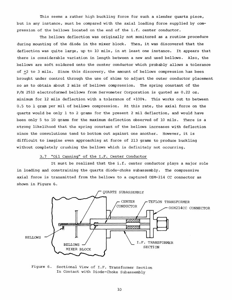
3.7 "Oil Canning" of the I.F. Center Conductor It must be realized that the i.f. center conductor plays a major role
in loading and constraining the quartz diode-choke subassembly. The compressive
axial force is transmitted from the bellows to a captured OSM-214 CC connector as
shown in Figure 6.
Figure 6. Sectional View of I.F. Transformer SectionIn Contact with Diode-Choke Subassembly
10
In particular, it should be noted that one mixer block with associated
i.f. transformer section gave recurrent difficulty in attempts to cool diodes
without producing open circuits. This mixer block was tried with 4 or 5 different
diodes but always produced a failure. Subsequently, it was discovered that the
teflon i.f. transformer was a much looser fit than usual for this unit so that, even
at room temperature, there was some play in the center conductor. Upon replacing
the teflon piece with one that gave a much snugger fit (the new piece was cooled to
77°K for insertion in the outer conductor) this mixer block cooled to 77°K without
producing a diode open circuit.
It appears that upon cooling the teflon transformer contracts substantially
thus allowing free play in the i.f. center conductor. Under these conditions, thecenter conductor "oil cans" over to one side or the other under the influence of the
axial stress plus any other loads transmitted from the OSM connector. The amount offree movement available at the bellows-quartz location is substantial since this
motion is magnified by the distance from the teflon transformer.The lateral force available at the bellows to be transferred at the time
"oil canning" of the center conductor occurs results from both the axial compressive
force loading the bellows as well as any built in stress at the OSM connector that isbeing sustained by the teflon bushing. The axial force is of the order of 1.5 to 3grams based on the previously discussed spring constant and a deflection of about3.3 mils which includes 1.3 mil of differential contraction between the brass blockand the quartz substrate. Since this force remains substantially along the axialdirection, it is not believed that a lateral component of about 1 gram could begenerated to provide the minimum bending force necessary to open circuit the diode.
However, the unbalanced stress released by the shrinkage of the teflon bushing couldeasily generate a force this large. In other words, the lateral location of the i.f.center conductor at the bellows end is determined by the teflon bushing plus thedirection the center conductor leaves the OSM connector in the free state. When the
teflon bushing gives up its constraining action through shrinkage, the center conductor
returns to the position determined by the way it leaves the connector. Under these
circumstances, the lateral force available at the bellows end may easily be assumed
to exceed I gram. The fact that teflon tends to cold flow under load implies that
tightening this bushing at room temperature is a temporary solution to this problem
and that a more permanent solution lies in a different choice of material and/or
another means of constraining motion of the i.f. center conductor under cryogenic
circumstances.
11

4.0 Summary of Remedies, Applied and RecommendedTwo separate lists will be given to show those remedies that have been
applied to improve the yield of coolable diodes for the 80-120 GHz in the recent
past and to indicate areas where further changes may provide greatly increaseddiode service life and reliability. The remedies applied were done so on a
piecemeal basis as the effects involved became better understood. It is the presentintention to at least incorporate all these procedures and improvements into each
existing mixer block as the diodes are replaced for the next time (all 8 mixer blocksare presently servicable,with good diodes at the time of this writing).
A. Remedies Applied:
1. Be sure whiskers are fabricated from annealed phos. bronze wire
and are properly pointed and plated.
2. Be sure the Eastman 910 cement is fresh and is setting up
properly.3. Minimize flexure of the quartz substrate in the whiskering
jig. This fixture in its present condition is barely usable
and should be replaced with a new design which eliminatesflexure by fully supporting the quartz substrate.
4. Use the second assembly technique described for mounting the
diode-choke assembly in the mixer block with particularattention paid to making the indium land flat and centeringthe quartz in the channel
5. Accurately control the compression of the bellows on the i.f.center conductor to be 2 mils through the use of shims betweenthe i.f. transformer section and the osm connector.
6. Use very snugly fitting teflon transformers (bushings) in the
i.f. section to minimize free play in the center conductor.
If possible shrink the teflon by cooling to 77°K prior toinserting in outer conductor. The teflon should be changedevery time the diode is replaced since cold flow will causean increase of clearance for this part.
B. Recommended Further Remedies:
1. Very accurate control of whisker pointing and gold platingthickness to minimize plastic deformation.
12

B. (continued)
2. Use of whisker deflection greater than 1.5 pm. (This mustbe approached with caution since 2.0 pm was tried and produceda punched through device upon cooling).
3. Change the whisker material to reduce contraction, try tungsten,
molybdenum, tantalum, etc.4. Change from quartz to thermally matched glass substrate to
minimize differential contraction.
5. Change from teflon to another dielectric for i.f. transformer
to eliminate cold flow and minimize dimensional change, tryirradiated polypropylene.
5. Implications for Future Cryogenic MixersThe implications for future cryogenic mixers are that intensive structural
and thermal analysis needs doing before committing to a design with greatly reducedcross sectional area for the quartz substrate. The 150 GHz mixer is presently designed
with a 3 mil thick quartz substrate of the same configuration discussed here to preventmoding problems. Since beam strength (resistance to flexure) varies as thicknesscubed, it is it apparent that this substrate is already 8 times weaker than that ofthe 80 to 120 GHz mixer discussed here. In other words, only 1/8 gram transverseforce might be required to open circuit the diode. For a 230 GHz mixer the problem
is yet more severe. This needs to be looked at very closely. A different configurationfor mounting the diode providing improved mechanical and thermal stability appearshighly desirable.
13