naval postgraduate · pdf filedistribution code 13. ... at the naval postgraduate school...
TRANSCRIPT
NAVAL
POSTGRADUATE SCHOOL
MONTEREY, CALIFORNIA
THESIS
Approved for public release; distribution is unlimited
FIELD PROGRAMMABLE GATE ARRAY CONTROL OF POWER SYSTEMS IN GRADUATE STUDENT LABORATORIES
by
Joseph E. O’Connor
March 2008
Thesis Advisor: Alexander Julian Second Reader: Roberto Cristi

THIS PAGE INTENTIONALLY LEFT BLANK
i
REPORT DOCUMENTATION PAGE Form Approved OMB No. 0704-0188Public reporting burden for this collection of information is estimated to average 1 hour per response, including the time for reviewing instruction, searching existing data sources, gathering and maintaining the data needed, and completing and reviewing the collection of information. Send comments regarding this burden estimate or any other aspect of this collection of information, including suggestions for reducing this burden, to Washington headquarters Services, Directorate for Information Operations and Reports, 1215 Jefferson Davis Highway, Suite 1204, Arlington, VA 22202-4302, and to the Office of Management and Budget, Paperwork Reduction Project (0704-0188) Washington DC 20503. 1. AGENCY USE ONLY (Leave blank)
2. REPORT DATE March 2008
3. REPORT TYPE AND DATES COVERED Master’s Thesis
4. TITLE AND SUBTITLE Field Programmable Gate Array Control of Power Systems in Graduate Student Laboratories 6. AUTHOR(S) Joseph E. O’Connor
5. FUNDING NUMBERS
7. PERFORMING ORGANIZATION NAME(S) AND ADDRESS(ES) Naval Postgraduate School Monterey, CA 93943-5000
8. PERFORMING ORGANIZATION REPORT NUMBER
9. SPONSORING /MONITORING AGENCY NAME(S) AND ADDRESS(ES)
N/A
10. SPONSORING/MONITORING AGENCY REPORT NUMBER
11. SUPPLEMENTARY NOTES The views expressed in this thesis are those of the author and do not reflect the official policy or position of the Department of Defense or the U.S. Government. 12a. DISTRIBUTION / AVAILABILITY STATEMENT Approved for public release; distribution is unlimited
12b. DISTRIBUTION CODE
13. ABSTRACT (maximum 200 words) The Department of Electrical and Computer Engineering at the Naval Postgraduate
School (NPS) continuously develops new design and education resources for students. One area of focus for students in the Power Electronics curriculum track is the development of a design center that explores Field Programmable Gate Array (FPGA) control of power electronics. Utilizing Mathworks® and XILINX® software to interface the FPGA with power converters, students gain experience with digital design, simulation, and hardware testing. This thesis focuses on the design, implementation and testing of a Student Design Center (SDC) employing an FPGA based digital controller. This thesis especially concentrates on the hardware interface between the FPGA and the power electronics and the development of laboratory procedures for students utilizing the design center.
15. NUMBER OF PAGES
99
14. SUBJECT TERMS Field Programmable Gate Array (FPGA), Voltage Converter, Graduate Student Laboratories
16. PRICE CODE
17. SECURITY CLASSIFICATION OF REPORT
Unclassified
18. SECURITY CLASSIFICATION OF THIS PAGE
Unclassified
19. SECURITY CLASSIFICATION OF ABSTRACT
Unclassified
20. LIMITATION OF ABSTRACT
UU NSN 7540-01-280-5500 Standard Form 298 (Rev. 2-89) Prescribed by ANSI Std. 239-18

ii
THIS PAGE INTENTIONALLY LEFT BLANK

iii
Approved for public release; distribution is unlimited
FIELD PROGRAMMABLE GATE ARRAY CONTROL OF POWER SYSTEMS IN GRADUATE STUDENT LABORATORIES
Joseph E. O’Connor
Captain, United States Marine Corps B.S., University of South Carolina, 2001
Submitted in partial fulfillment of the requirements for the degree of
MASTER OF SCIENCE IN ELECTRICAL ENGINEERING
from the
NAVAL POSTGRADUATE SCHOOL March 2008
Author: Joseph E. O’Connor
Approved by: Alexander L. Julian Thesis Advisor
Roberto Cristi Second Reader
Jeffrey B. Knorr Chairman, Department of Electrical and Computer Engineering

iv
THIS PAGE INTENTIONALLY LEFT BLANK
v
ABSTRACT
The Department of Electrical and Computer Engineering
at the Naval Postgraduate School (NPS) continuously
develops new design and education resources for students.
One area of focus for students in the Power Electronics
curriculum track is the development of a design center that
explores Field Programmable Gate Array (FPGA) control of
power electronics. Utilizing Mathworks® and XILINX®
software to interface the FPGA with a voltage source
converter (VSC), students gain experience with digital
design, simulation, and hardware testing. This thesis
focuses on the design, implementation and testing of a
Student Design Center (SDC) employing an FPGA based digital
controller. This thesis especially concentrates on the
hardware interface between the FPGA and the power
electronics and the development of laboratory procedures
for students utilizing the design center.

vi
THIS PAGE INTENTIONALLY LEFT BLANK

vii
TABLE OF CONTENTS
I. INTRODUCTION ............................................1 A. BACKGROUND .........................................1 B. RESEARCH OBJECTIVES ................................2 C. APPROACH ...........................................2 D. RELATED WORK .......................................3 E. THESIS ORGANIZATION ................................4 F. CHAPTER SUMMARY ....................................4
II. STUDENT DESIGN CENTER OVERVIEW ..........................7 A. FIELD PROGRAMMABLE GATE ARRAY ......................7
1. Overview ......................................7 2. SDC FPGA ......................................8
B. VOLTAGE SOURCE CONVERTER AND SPACE VECTOR MODULATION ........................................12
C. HARDWARE AND SOFTWARE .............................18 D. SDC COMPUTER AIDED DESIGN ARCHITECTURE ............19
1. VHDL Synthesis Using ISE Foundation ..........23 2. Hardware Interface Using ChipScope™ Pro ......24
E. CHAPTER SUMMARY ...................................26 III. PRINTED CIRCUIT BOARD DESIGN AND TESTING ...............29
A. SCHEMATIC LAYOUT AND PCB DESIGN ...................29 B. MAJOR COMPONENT PACKAGING .........................32 C. ANALOG-DIGITAL CONVERSION OF FEEDBACK SIGNALS .....33
1. Power Requirements ...........................35 2. Conditioning of Sampled Signals ..............36
D. CHAPTER SUMMARY ...................................41 IV. CONCLUSIONS AND RECOMMENDATIONS ........................43
A. SUMMARY ...........................................43 B. CONCLUSIONS .......................................43 C. RECOMMENDATIONS FOR FURTHER RESEARCH ..............44
APPENDIX A: PCB SCHEMATICS AND VIRTEX-4TM BOM.............45 APPENDIX B: VIRTEX-4TM CONDENSED USER'S GUIDE.............53
A. VIRTEX-4TM DEVELOPMENT BOARD COMPONENTS............53 1. DDR SDRAM ....................................53 2. Clock Sources ................................53 3. 10/100 Ethernet PHY ..........................54 4. LCD Panel ....................................55 5. RS232 Interface ..............................56 6. User DIP and PB Switches .....................56 7. User LEDs ....................................57 8. User GPIO ....................................57 9. Configuration and Debug Ports ................58

viii
a. JTAG Gain ...............................58 b. System ACE Module Connector .............59 c. System ACE Controller Signal
Description .............................60 d. Serial Flash ............................61 e. JTAG Chain on the Virtex-4™ Development
Board ...................................63 f. Configuration Flash on the Virtex-4™
Development Board .......................64 g. JTAG Port ...............................65 h. Configuration Modes .....................66
10. Voltage Regulators ...........................66 11. Bank I/O Voltage .............................68 12. P160 Expansion Module Signal Assignments .....68
APPENDIX C: SEMITEACH® POWER CONVERTER ...................71 LIST OF REFERENCES ..........................................73 INITIAL DISTRIBUTION LIST ...................................77
ix
LIST OF FIGURES
Figure 1. Student Design Center...........................xv Figure 2. FPGA Architecture [From [8]].....................8 Figure 3. FPGA Logic Block [From [8]]......................9 Figure 4. XILINX® Virtex-4™ Development Board [From [9]]..10 Figure 5. Virtex-4TM Development Board Block Diagram [From
[9]]............................................11 Figure 6. Virtex-4™ Development Board Layout [From [10]]..12 Figure 7. SEMITEACH® Voltage Source Converter [From
[11]]...........................................13 Figure 8. SEMITEACH® VSC Schematic [From [11]]............13 Figure 9. Space Vector Modulation Hexagon [From [12]].....14 Figure 10. Simple Converter Schematic [From [12]]..........14 Figure 11. Switching Pattern for Each Sector [From [12]]...17 Figure 12. Software Interface Block Diagram [From [9]].....18 Figure 13. SDC Hardware Configuration [From [15]]..........19 Figure 14. Computer Aided Design Architecture [From [15]]..20 Figure 15. XILINX® Blocks for Simulink® Library Browser....21 Figure 16. DC-DC Buck Converter Simulink® Model [After
[16]]...........................................22 Figure 17. System Generator Block and Menu.................23 Figure 18. XILINX® ISE Window..............................24 Figure 19. ChipScope™ Pro Window...........................25 Figure 20. The “Configure” Command under the “Device”
Menu............................................25 Figure 21. VIO Console in ChipScope™ Pro...................26 Figure 22. Analog Signal Interface PCB.....................30 Figure 23. PCB123® 3-D View and Photo of Power Source
Interface PCB...................................31 Figure 24. Student Design Center System Interface..........32 Figure 25. Student Design Center...........................33 Figure 26. Four Channel AD-7864 Timing Diagram [From
[17]]...........................................34 Figure 27. Simulink® Digital Calibration of Signals [After
[16]]...........................................35 Figure 28. Lowpass Filter Magnitude Response...............39 Figure 29. Symmetric FIR Butterworth Filter [After [20]]...39 Figure 30. Original and Filtered 1kHz Signal...............40 Figure 31. Original and Filtered 5kHz Signal...............40 Figure 32. Original and Filtered 10kHz Signal..............40 Figure 33. DDR SDRAM Interface.............................53 Figure 34. Clock Sources on the Virtex-4™ board............54 Figure 35. 10/100 Ethernet Interface.......................55 Figure 36. RS232 Interface.................................56

x
Figure 37. Vitex-4 LC Development Board JTAG Chain.........59 Figure 38. System ACE module connecter.....................60 Figure 39. Virtex-4™ Configuration Interface...............62 Figure 40. Virtex-4™ Development Board JTAG Chain..........64 Figure 41. Serial Flash Configuration Interface............65 Figure 42. PC4 JTAG Port Connector.........................66 Figure 43. Voltage Regulators..............................67 Figure 44. SEMITEACH® Power Converter [From [11]]..........71

xi
LIST OF TABLES
Table 1. LCD Interface Signals...........................55 Table 2. Push Button Switch Pin Assignments..............56 Table 3. DIP Switch Pin Assignments......................57 Table 4. LED Pin Assignments.............................57 Table 5. GPIO Pin Assignments............................58 Table 6. GPIO Pin Assignments............................61 Table 7. FPGA SPI Interface Pin Assignments..............63 Table 8. JTAG Chain Jumper Settings......................64 Table 9. FPGA Configuration Mode Jumper Settings.........66 Table 10. FPGA Configuration Mode Jumper Settings.........67 Table 11. I/O Bank Voltages...............................68 Table 12. P160 Connector Pin Assignments..................69 Table 13. P160 Connector Pin Assignments..................70

xii
THIS PAGE INTENTIONALLY LEFT BLANK

xiii
LIST OF SYMBOLS, ACRONYMS, AND ABBREVIATIONS
A Amps
AC Alternating Current
A/D Analog to Digital Converter
BNC Bayonet Nut Connector
BOM Bill of Materials
CAD Computer Aided Design
COTS Commercial-Off-The-Shelf
dB Decibel
DC Direct Current
DSP Digital Signal Processor
EMI Electromagnetic Interference
ESD Electrostatic Discharge
FPD Field Programmable Device
FPGA Field Programmable Gate Array
HDL Hardware Description Language
IEEE Institute of Electrical and Electronics Engineers
IGBT Insulated Gate Bipolar Transistor
kHz Kilohertz
LUT Lookup Table
LPF Lowpass Filter
NPS Naval Postgraduate School
OPAMP Operational Amplifier
PCB Printed Circuit Board
RAM Random Access Memory
SDC Student Design Center
SOP Standard Operating Procedure
SVM Space Vector Modulation
V Volts
VHDL Very-High-Speed-Integrated-Circuit Hardware Description language
VSC Voltage Source Converter

xiv
THIS PAGE INTENTIONALLY LEFT BLANK

xv
EXECUTIVE SUMMARY
The Student Design Center (SDC) at the Naval
Postgraduate School (NPS) Electrical Engineering Department
(Solid State Microelectronics and Power Systems track) was
created to expose students to the process of basic solid
state power design and control, also known as "digital
power". The SDC enables students to make accurate
predictions of voltage source converter (VSC) behavior
using software simulation; furthermore, the SDC allows
students to test their simulations on the actual hardware
to verify results.
The primary components of the SDC architecture are a
Field Programmable Gate Array (FPGA), a VSC (augmented by
other commercial, off-the-shelf components for various
laboratories), a circuit board interface between the FPGA
and the VSC, a circuit board interface between the FPGA and
the power source, and a desktop computer. The design
center is shown in Figure 1.
Figure 1. Student Design Center.

xvi
The SDC utilizes Mathworks' Simulink® software to
generate hardware control simulations and run virtual
experiments on VSCs and other power systems. XILINX®
software produces Verilog Hardware Description Language
(VHDL) code to interface the FPGA with hardware components;
hence, basic knowledge of programming is required, but
prior experience with VHDL coding is unnecessary.
The Semikron® VSC used in the SDC employs three
parallel-connected half-bridges with an IGBT-diode brake
for protection. Custom interface Printed Circuit Boards
(PCBs) were designed, constructed, and tested to interface
the FPGA with the VSC and the switching power source. The
FPGA controls two analog-to-digital (A/D) converters for
sampling VSC load currents and voltages. The FPGA was
programmed with XILINX® software (embedded in the Simulink®
model) and used to drive the VSC. The PCBs were thoroughly
tested for compatibility and faults, and a digital low pass
filter was designed and installed to reduce high frequency
interference in the sampled signals. Four laboratory
systems (buck converter, boost converter, H-bridge DC/AC
converter and a diode-rectifier) were built to augment the
VSC for various laboratories used in graduate power
electronics courses.
The main thrust of this thesis was the exploration of
the interface between the FPGA and the VSC and the actual
construction and testing of the SDC. Emphasis was placed
on the design, layout, and testing of each PCB as well as
techniques used to minimize or eliminate adverse
performance due to electromagnetic interference.

xvii
A secondary objective was to present the reader with a
background and overview of the hardware and software used
in the SDC including a brief description of current FPGA
technology and its wide variety of applications in academic
settings. A detailed derivation of Space Vector Modulation
(SVM) was accomplished since it is the VSC control
technique used in power electronics laboratories at NPS.
Finally, the last objective was to develop a Standard
Operating Procedure (SOP) for laboratories conducted in the
SDC in order to provide students with a better
understanding of design flow prior to execution and to
supplement laboratory assignments as a resource for
frequently asked questions.

xviii
THIS PAGE INTENTIONALLY LEFT BLANK

xix
ACKNOWLEDGMENTS
I would like to express my sincere appreciation to the
faculty and staff of the Naval Postgraduate School for
their dedication to the ideals of higher education. You
make it possible for professional military men and women to
pursue their academic goals while supporting their family
and this great country.
Thank you to Professor Julian for his genuine outlook
on my educational experience and for his common-sense
approach to life in general. Working side-by-side with him
was an honor and privilege. I hope his attitude towards
teaching and mentoring students is recognized by the
department and used as a template for future hires.
Special thanks to the laboratory technicians James
Calusdian, Jeff Knight, Warren Rogers, and Petty Officer
McGill who were always ready and willing to help.
Thank you to my parents, Thomas and Kathleen O'Connor,
for instilling a good work ethic and a passion for
"figuring things out."
Finally, and most importantly, thank you to my wife,
Kelly, and to my children. Without you I would not be the
man and Marine I am today. You give my life meaning and
purpose, and I hope I never let you down.

xx
THIS PAGE INTENTIONALLY LEFT BLANK

1
I. INTRODUCTION
A. BACKGROUND
The Student Design Center (SDC) for the Naval
Postgraduate School Electrical Engineering Department
(Solid State Microelectronics and Power Systems track) was
created for the purpose of exposing students to the process
of transforming performance requirements into basic design.
The center exposes students to basic power electronics
design, enables accurate behavior predictions using
software simulation, and allows students to test their
simulations on the actual hardware to verify results.
Students enrolled in power electronics courses complete
assigned laboratories and become thoroughly indoctrinated
in the design simulation and testing process. Each
laboratory strives to give students practical problems in a
real-world environment while preparing them for future
study in product design and control [1].
The primary components of the SDC architecture are a
Field Programmable Gate Array (FPGA); a voltage source
converter (augmented by other commercial, off-the-shelf
equipment for various laboratories); a Printed Circuit
Board (PCB) interface between the FPGA and the VSC; a PCB
interface between the FPGA and the power source; and a
desktop computer. Students use Mathworks' Simulink®
software to generate hardware control simulations and run
virtual experiments on VSCs and other power systems.
XILINX® software produces Verilog Hardware Description
Language (VHDL) code to interface the FPGA with hardware

2
components; hence, basic knowledge of programming is
required, but prior experience with VHDL coding is
unnecessary.
B. RESEARCH OBJECTIVES
The main thrust of this thesis is the exploration of
the interface between the FPGA with the VSC, and the FPGA
with the switching power source. Emphasis is placed on the
design, layout, and testing of each interface PCB as well
as techniques used to minimize or eliminate adverse
performance due electromagnetic interference.
A secondary objective is to present the reader with a
background and overview of the hardware and software used
in the SDC, present a brief overview of current FPGA
technology and its wide variety of applications in academic
settings, and develop the voltage conversion technique used
in Power Electronics laboratories.
Finally, a Standard Operating Procedure (SOP) is
developed to provide graduate students with a better
understanding of design flow prior to executing
experiments. The SOP is intended to supplement laboratory
assignments as a resource for frequently asked questions.
C. APPROACH
The equipment used to build the SDC included a
Semikron® VSC employing three parallel-connected half-
bridges with an Insulated Gate Bipolar Transistor (IGBT)
diode brake for protection; a MEMECTM Virtex-4™ Development
Board containing a XILINX® FPGA; and a stand-alone personal
computer workstation incorporating a Pentium® processor.
Custom interface PCBs were designed, constructed, and
3
tested to interface the FPGA with the VSC, and the FPGA
with the switching power source. The analog signal
interface PCB included an output control for the VSC and
two analog-to-digital (A/D) converters for detecting load
currents and voltages. The FPGA was programmed with
XILINX® software (imbedded in the Simulink® model) and used
to drive the VSC. The PCB was thoroughly tested for
compatibility and faults [2]. A digital low pass filter
was designed to reduce high frequency interference from the
converted signals. Four laboratory systems (buck converter,
boost converter, H-bridge DC/AC converter and a diode-
rectifier) were built to augment the VSC for various
laboratories used in graduate power electronics courses.
Finally, the SDC SOP was developed and implemented.
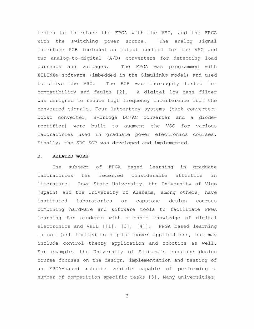
D. RELATED WORK
The subject of FPGA based learning in graduate
laboratories has received considerable attention in
literature. Iowa State University, the University of Vigo
(Spain) and the University of Alabama, among others, have
instituted laboratories or capstone design courses
combining hardware and software tools to facilitate FPGA
learning for students with a basic knowledge of digital
electronics and VHDL [[1], [3], [4]]. FPGA based learning
is not just limited to digital power applications, but may
include control theory application and robotics as well.
For example, the University of Alabama's capstone design
course focuses on the design, implementation and testing of
an FPGA-based robotic vehicle capable of performing a
number of competition specific tasks [3]. Many universities
4
around the world are recognizing the value, both monetary
and educational, of incorporating FPGA based learning in
their academic institutions.
E. THESIS ORGANIZATION
• Chapter I introduces research goals and presents
the organization of the thesis.
• Chapter II presents the SDC's hardware and
software, gives background information on VSC
control principles, and covers the computer aided
design (CAD) layout of the SDC.
• Chapter III explores the design, construction,
and testing of the analog signal interface PCB
and power interface PCB.
• Chapter IV addresses conclusions and future
research opportunities.
• Appendix A provides information on the XILINX®
Virtex-4™ Development Board.
• Appendix B contains PCB schematics and the
Virtex-4™ Development Board's bill of materials
(BOM).
• Appendix C provides information on the SEMITEACH®
VSC.
F. CHAPTER SUMMARY
This chapter gave a brief introduction of SDC
objectives, research goals, and the approach taken to meet
those goals. It concluded with the organization of this
thesis. Chapter II introduces the reader to the hardware

5
and software used in the SDC, presents a background in FPGA
technology, and discusses the voltage conversion technique
used in Power Electronics laboratories.

6
THIS PAGE INTENTIONALLY LEFT BLANK

7
II. STUDENT DESIGN CENTER OVERVIEW
A. FIELD PROGRAMMABLE GATE ARRAY
1. Overview
A Field Programmable Device (FPD) is a general term
that refers to any type of integrated circuit used for
implementing digital hardware, where the chip can be
configured by the end user to realize different designs.
Programming of such a device usually involves interfacing
the device with specially designed programming software
[5]. An FPGA is a semiconductor device containing
programmable logic components and programmable
interconnects. The programmable logic components can be
programmed to duplicate the functionality of basic logic
gates or more complex combination functions such as
decoders and simple mathematical functions [6]. A major
advantage of this technology is that FPGAs can execute
codes in parallel whereas Digital Signal Processors (DSPs)
execute codes in series. Hence, FPGA's do not have to
"store" as much data as DSPs, and the need for large
amounts of Random Access Memory (RAM) degrades
significantly [7]. Another advantage of using FPGAs is
their ability to work with whatever wordlength the
programmer chooses. Whereas DSP processors must be selected
to handle the longest wordlength that occurs in the code
(thereby reducing efficiency when processing shorter
wordlengths) FPGAs allow greater flexibility and efficiency
by utilizing the smallest necessary wordlengths [8].

8
2. SDC FPGA
XILINX®, a leading manufacturer of FPGA's, primarily
builds array-based circuits. These circuits incorporate
chips comprised of two dimensional arrays of logic blocks
that can be interconnected via horizontal and vertical
routing channels [8]. An example of a generic, two-
dimensional FPGA architecture is shown in Figure 2.
Figure 2. FPGA Architecture [From [8]].
The key difference between an FPGA and a "gate array"
is that the former can be reprogrammed in the “field” since
the logic program is changeable. Furthermore, whereas
early gate arrays were composed of NAND gates, FPGA's are a
carefully balanced selection of multi-input logic,
flipflops, multiplexors and memory [8]. A typical layout
for an FPGA is shown in Figure 3.

9
Figure 3. FPGA Logic Block [From [8]].
For the XILINX® FPGA used in this thesis, each logic
block references Look-Up Tables (LUTs), which are small,
one-bit wide memory arrays. The LUT input is composed of
address lines while the output is a one-bit output of the
memory. A LUT with "K" inputs corresponds to a "2K x 1"
bit memory and can realize any logic function of its "K"
inputs by programming the logic function’s table directly
into the memory [5]. FPGA's provide an excellent
alternative for applications that require flexibility for
various applications while avoiding the extra cost of
multiple, hard-wired circuit boards. The SDC demands such
flexibility since various design criteria are presented to
students and the need to reprogram the board is essential.
For this thesis, a XILINX® Virtex-4™ Development Board
incorporating a XC4VLX25-10SF363 FPGA was utilized and is
shown in Figure 4.
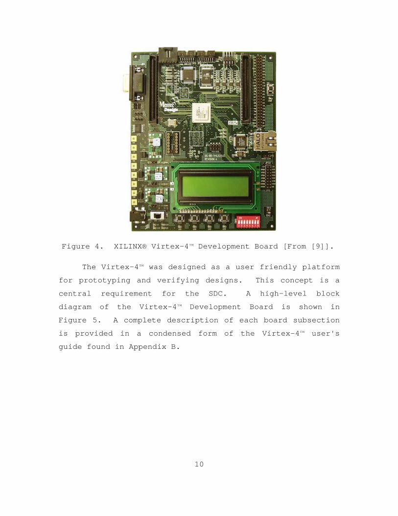
10
Figure 4. XILINX® Virtex-4™ Development Board [From [9]].
The Virtex-4™ was designed as a user friendly platform
for prototyping and verifying designs. This concept is a
central requirement for the SDC. A high-level block
diagram of the Virtex-4™ Development Board is shown in
Figure 5. A complete description of each board subsection
is provided in a condensed form of the Virtex-4™ user's
guide found in Appendix B.
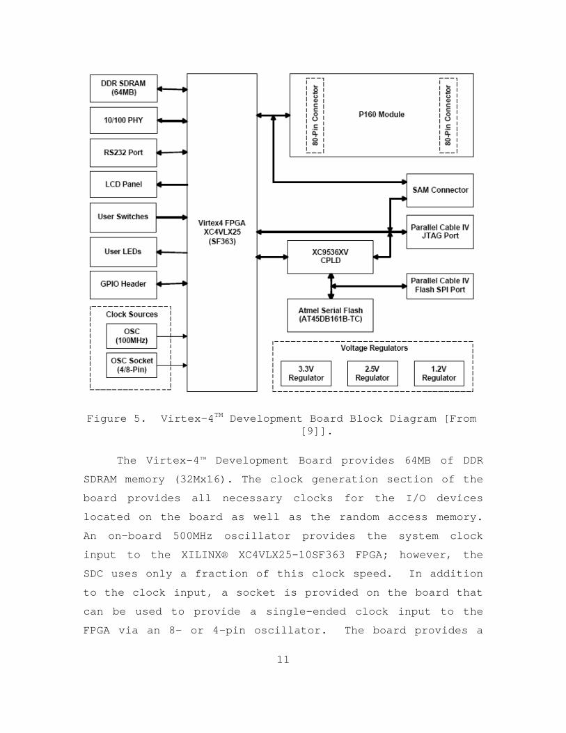
11
Figure 5. Virtex-4TM Development Board Block Diagram [From [9]].
The Virtex-4™ Development Board provides 64MB of DDR
SDRAM memory (32Mx16). The clock generation section of the
board provides all necessary clocks for the I/O devices
located on the board as well as the random access memory.
An on-board 500MHz oscillator provides the system clock
input to the XILINX® XC4VLX25-10SF363 FPGA; however, the
SDC uses only a fraction of this clock speed. In addition
to the clock input, a socket is provided on the board that
can be used to provide a single-ended clock input to the
FPGA via an 8- or 4-pin oscillator. The board provides a

12
10/100 Ethernet port for network connection and an 8-bit
interface to a 2x16 LCD panel. The board also provides
four user push button switches allowing an active low
signal to be generated when a given switch is pressed.
These switches can be remotely toggled using ChipScope™ Pro
software (addressed later in this chapter). A JTAG
connector is used as a port to load the software from a
desktop computer, and the 5.0V connector pin is used to
supply the main power to the card. The board has two
interface connectors that provide easy access to the PCB
interface [9]. An overview of the Virtex-4™ Development
Board's layout is shown in Figure 6.
Figure 6. Virtex-4™ Development Board Layout [From [10]].
B. VOLTAGE SOURCE CONVERTER AND SPACE VECTOR MODULATION
The VSC used in the SDC is a three-phase,
rectifier/converter specially equipped to allow students
visualization of every part. The VSC is contained inside
an external interface for safety and is produced by
13
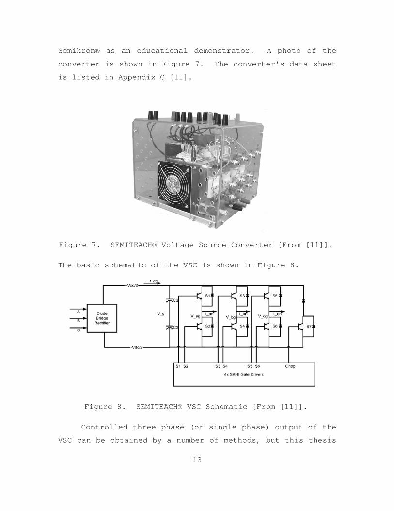
Semikron® as an educational demonstrator. A photo of the
converter is shown in Figure 7. The converter's data sheet
is listed in Appendix C [11].
Figure 7. SEMITEACH® Voltage Source Converter [From [11]].
The basic schematic of the VSC is shown in Figure 8.
Figure 8. SEMITEACH® VSC Schematic [From [11]].
Controlled three phase (or single phase) output of the
VSC can be obtained by a number of methods, but this thesis
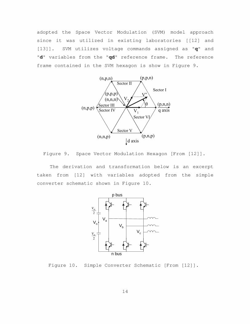
14
adopted the Space Vector Modulation (SVM) model approach
since it was utilized in existing laboratories [[12] and
[13]]. SVM utilizes voltage commands assigned as "q" and
"d" variables from the "qd" reference frame. The reference
frame contained in the SVM hexagon is show in Figure 9.
Sector ISector II
Sector IIISector IV
Sector V
Sector VI
(p,n,n)
(n,n,p) (p,n,p)
(n,p,n) (p,p,n)
(n,p,p) V1
V2V*
θq axis
d axis
(p,p,p)(n,n,n)
Figure 9. Space Vector Modulation Hexagon [From [12]].
The derivation and transformation below is an excerpt
taken from [12] with variables adopted from the simple
converter schematic shown in Figure 10.
Va
Vb
Vc
p bus
n bus
Vn
2dcV
2dcV
Figure 10. Simple Converter Schematic [From [12]].
15
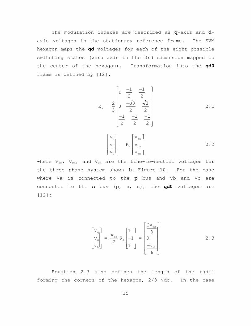
The modulation indexes are described as q-axis and d-
axis voltages in the stationary reference frame. The SVM
hexagon maps the qd voltages for each of the eight possible
switching states (zero axis in the 3rd dimension mapped to
the center of the hexagon). Transformation into the qd0
frame is defined by [12]:
s
1 11
2 22 3 3
K 0 3 2 2
1 1 1
2 2 2
− −⎡ ⎤⎢ ⎥⎢ ⎥
−⎢ ⎥= ⎢ ⎥⎢ ⎥− − −⎢ ⎥⎢ ⎥⎣ ⎦
2.1
q an
d s bn
0 cn
v v
v K v
v v
⎡ ⎤ ⎡ ⎤⎢ ⎥ ⎢ ⎥=⎢ ⎥ ⎢ ⎥⎢ ⎥ ⎢ ⎥⎣ ⎦⎣ ⎦
2.2
where Van, Vbn, and Vcn are the line-to-neutral voltages for
the three phase system shown in Figure 10. For the case
where Va is connected to the p bus and Vb and Vc are
connected to the n bus (p, n, n), the qd0 voltages are
[12]:
dc
q
dcd s
0 dc
2vv 1 3
vv K 1 0
2v 1 v
6
⎡ ⎤⎢ ⎥⎡ ⎤ ⎡ ⎤⎢ ⎥⎢ ⎥ ⎢ ⎥= − = ⎢ ⎥⎢ ⎥ ⎢ ⎥⎢ ⎥⎢ ⎥ ⎢ ⎥ −⎣ ⎦⎣ ⎦ ⎢ ⎥⎣ ⎦
2.3
Equation 2.3 also defines the length of the radii
forming the corners of the hexagon, 2/3 Vdc. In the case

16
where Va and Vb are connected to the p bus and Vc is
connected to the n bus (p,p,n), the qd0 voltages are [12]:
dc
q
dc dcd s
0dc
v3v 1
v vv K 1
2 3v 1
v6
⎡ ⎤⎢ ⎥
⎡ ⎤ ⎡ ⎤ ⎢ ⎥−⎢ ⎥ ⎢ ⎥ ⎢ ⎥= =⎢ ⎥ ⎢ ⎥ ⎢ ⎥
⎢ ⎥ ⎢ ⎥− ⎢ ⎥⎣ ⎦⎣ ⎦⎢ ⎥⎢ ⎥⎣ ⎦
2.4
The two states defined by Equations 2.3 and 2.4 forms
the sides of Sector I. When the reference voltage is in
this sector, these two states and the zero states are used
to produce an output voltage that, on average, equals the
reference voltage.
Now let Ts be the total switching period, and let T1
and T2 represent the amount of time spent on states (p, n,
n) and (p, p, n) respectively. The vectors V1 and V2 are
proportional to the time spent on each state [12]:
dc11
s
2vTv
T 3= 2.5
dc22
s
2vTv
T 3= 2.6
The law-of-sines can be used to find the duty cycles
for each state [12]:
*
1 2o
2v v vsin(60 ) sin( )3
= =− θ θ
2.7
Substituting Equations 2.5 and 2.6 into Equation 2.7
yields solutions for the time spent on each state [12]:
*
o1 s
dc
v 3T T sin(60 )
v= − θ 2.8
*
2 sdc
v 3T T sin( )
v= θ 2.9

17
The time spent on each state cannot exceed the total
switching period so the modulation index (mi) is between
zero and one [12]:
*
* dc
dc
vv 3mi ,0 mi 1,0 v
v 3= < < < < 2.10
Finally, the amount of time spent in the zero state is
the time remaining in the period [12]:
0 s 1 2T T T T= − − 2.11
When choosing a switching method for SVM,
consideration should be given to minimizing switching
events and minimizing distortion. Switching patterns for
each sector are shown in Figure 11. Switching states are
shown on the right, and time duration is on the left.
Figure 11. Switching Pattern for Each Sector [From [12]].
4 0T
4 0T
2 0T
2 1T
2 2T
2 2T
2 1T
4 0T
4 0T
2 0T
2 2T
2 1T
2 1T
2 2T
Sector II Sector I
pnn
pnn
ppn
ppn
ppp
nnn
nnn
npn
npn
ppn
ppn
ppp
nnn
nnn
4 0T
4 0T
2 0T
2 1T
2 2T
2 2T
2 1T
4 0T
4 0T
2 0T
Sector IV Sector III
npn
npn
npp
npp
ppp
nnn
nnn
nnp
nnp
npp
npp
ppp
nnn
nnn
4 0T
4 0T
2 0T
2 1T
2 2T
2 2T
2 1T
4 0T
4 0T
2 0T
Sector VI Sector V
nnp
nnp
npp
npp
ppp
nnn
nnn
pnn
pnn
pnp
pnp
ppp
nnn
nnn
2 2T
2 1T
2 1T
2 2T
2 2T
2 1T
2 1T
2 2T
ab
cd
e

18
C. HARDWARE AND SOFTWARE
The SDC utilizes Simulink® for modeling power
electronics systems and for running simulations to test
designs. Simulink® enables multi-domain simulation and
model-based design for dynamic systems and provides an
interactive graphical environment as well as a customizable
set of block libraries. Most importantly, Simulink®
enables model analysis and diagnostics tools to ensure
model consistency and identify modeling errors prior to
hardware setup and testing [14].
XILINX® software produces VHDL code from the Simulink®
model in order to program the FPGA. VHDL is the most
commonly used design-entry language for field-programmable
gate arrays and learning the code is not a trivial task;
however, XILINX® enables the student to compile VHDL code
without becoming proficient in VHDL programming. The block
diagram for loading VHDL from the computer to the FPGA is
shown in Figure 12.
Figure 12. Software Interface Block Diagram [From [9]].
Once the VHDL code is obtained, it is converted to a
netlist and verified again using XILINX® Project Navigator.

19
Project Navigator allows the netlist to be compiled into a
form that can be directly loaded into the FPGA. It also
reports on the percentage of the FPGA usage. After
verification, the netlist can be fitted to the FPGA by
XILINX® Impact using a process called place-and-route. The
graphical interface is very easy to use by right-clicking
on the icon and selecting the appropriate file to load [9].
D. SDC COMPUTER AIDED DESIGN ARCHITECTURE
A block diagram of the SDC hardware configuration
including Computer Aided Design (CAD) tools, including the
Semikron® power module, passive components, and measuring
instruments, are shown in Figure 13.
Computer(Matlab & Xilinx
software)
FPGAdevelopment kit
FPGA dev. kit toSemikron module
interface (Circuit board)
Semikron module
Three-phase rectifier +
inverter with brakechopper
Resistor/inductorLoad
DC inductor &Resistor load
Inductor/Capacitorfilter with an
inductor/resistorload
Oscilloscopevoltage metervoltage probecurrent probepower meter
CAD Tools
Figure 13. SDC Hardware Configuration [From [15]].
The design process is summarized as follows: A
Simulink® is developed to simulate a power system.
Elements of the model internal to the FPGA are designed
using the System Generator library. The rest of the system
is designed using Simulink® library blocks. Once the
system is modeled, VHDL code is generated for the portion
of the simulation controlled by the FPGA. After the VHDL
is generated, the project is loaded into ISE Foundation

20
software and the design is synthesized. Then the program
is uploaded into the FPGA through the JTAG cable, and
ChipScope™ Pro is used to communicate with the target
hardware. Finally, data is downloaded from the FPGA and
imported into Matlab for measurement and plotting. The CAD
architecture is shown in Figure 14.
Simulink simulation of power electronics and
electric machines
(using a Xilinx blocksetinside Simulink)
Xilinx ISE Foundationgenerates programmingfile for FPGA from VHDL
Sy stemGenerator
System Generatorproduces VHDL code
Xilinx XC4VLX25 FPGA is programmed through the JTAG programming cable
JTAG cable
Digital control of target hardware through custom
interface card(includes A/D converters
and digital I/O)
Control and data acquisition from FPGA via JTAG cable using
ChipScope Pro software
Figure 14. Computer Aided Design Architecture [From [15]].
The XILINX® library blocks inside the Simulink®
library browser behave like other library blocks during
simulation. A screen snapshot of the Simulink® library
browser with the XILINX® blocks highlighted is shown in
Figure 15.

21
Figure 15. XILINX® Blocks for Simulink® Library Browser.
Every simulation that has System Generator library
blocks inside must have the System Generator block at the
top level. Note the System Generator block in the Buck-
Converter Laboratory model shown in Figure 16.
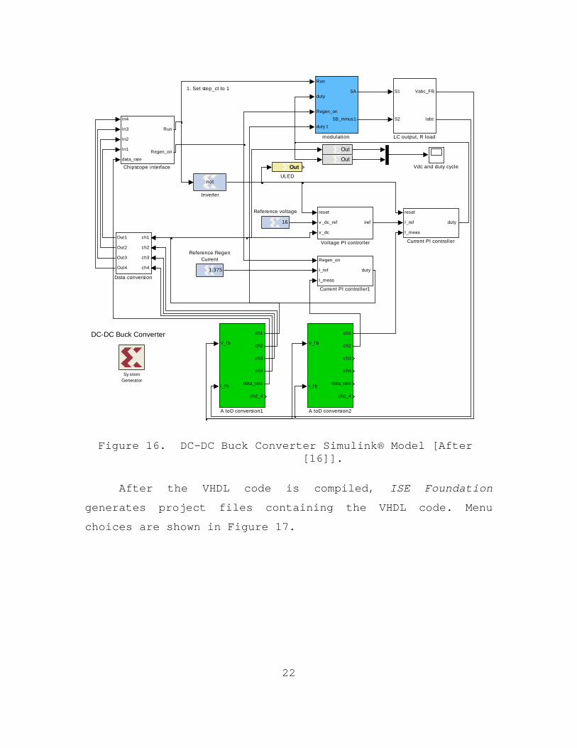
22
Figure 16. DC-DC Buck Converter Simulink® Model [After [16]].
After the VHDL code is compiled, ISE Foundation
generates project files containing the VHDL code. Menu
choices are shown in Figure 17.
1. Set step_ct to 1
DC-DC Buck Converter
Run
duty
Regen_on
duty 1
SA
SB_minus1
modulation
reset
v _dc_ref
v _dc
iref
Voltage PI controller
Vdc and duty cycle Out ULED
16
Reference voltage
1.375
Reference RegenCurrent
S1
S2
Vabc_FB
Iabc
LC output, R load
not
Inverter
Out
Out
ch1
ch2
ch3
ch4
Out1
Out2
Out3
Out4
Data conversion
Regen_on
I_ref
I_meas
duty
Current PI controller1
reset
I_ref
I_meas
duty
Current PI controller
In4
In3
In2
In1
data_rate
Run
Regen_on
Chipscope interface
V_f b
I_f b
ch1
ch2
ch3
ch4
data_rate
ch2_4
A toD conversion2
V_f b
I_f b
ch1
ch2
ch3
ch4
data_rate
ch2_4
A toD conversion1
Sy stemGenerator

23
Figure 17. System Generator Block and Menu.
1. VHDL Synthesis Using ISE Foundation
The design is synthesized using ISE Foundation
software by opening the project file, generating the
program file, and configuring the device in Impact. Once
synthesized, the programming file is generated and the FPGA
is programmed. The ISE Foundation window is shown in
Figure 18.
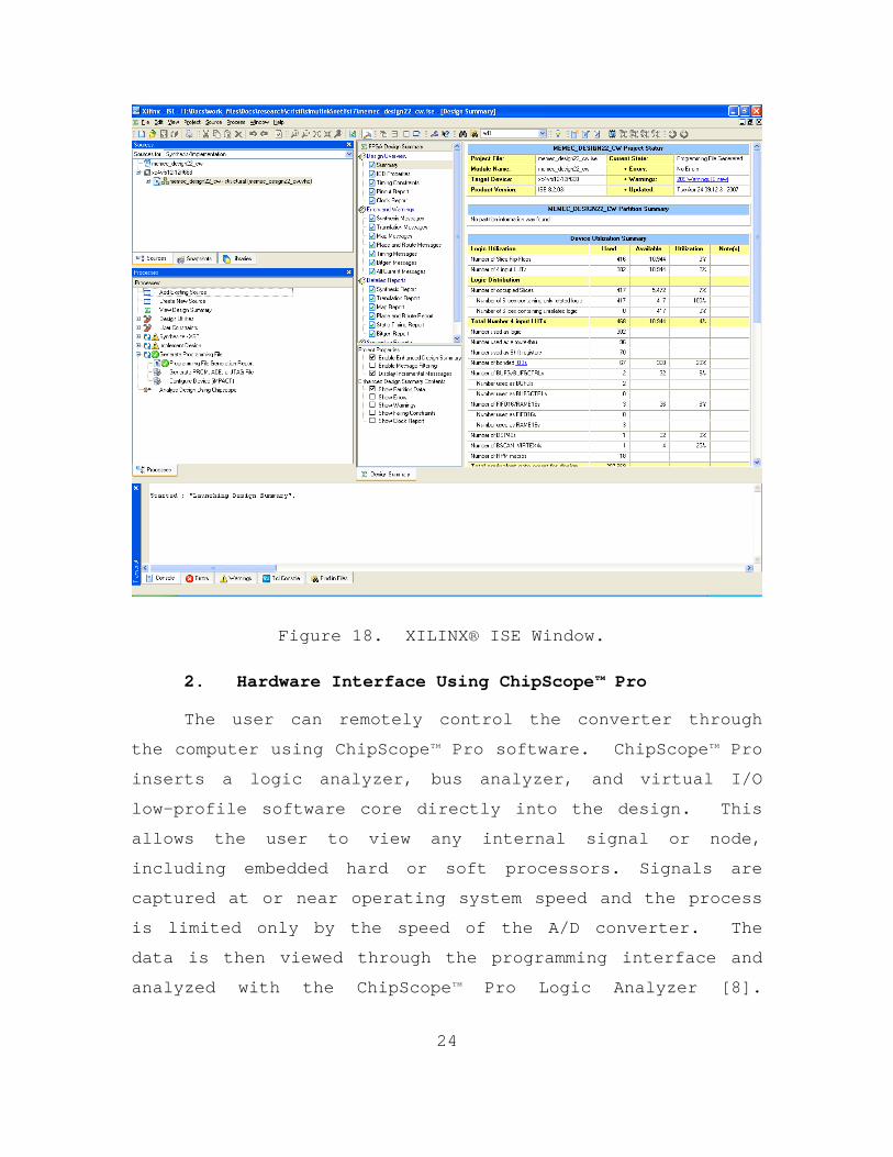
24
Figure 18. XILINX® ISE Window.
2. Hardware Interface Using ChipScope™ Pro
The user can remotely control the converter through
the computer using ChipScope™ Pro software. ChipScope™ Pro
inserts a logic analyzer, bus analyzer, and virtual I/O
low-profile software core directly into the design. This
allows the user to view any internal signal or node,
including embedded hard or soft processors. Signals are
captured at or near operating system speed and the process
is limited only by the speed of the A/D converter. The
data is then viewed through the programming interface and
analyzed with the ChipScope™ Pro Logic Analyzer [8].
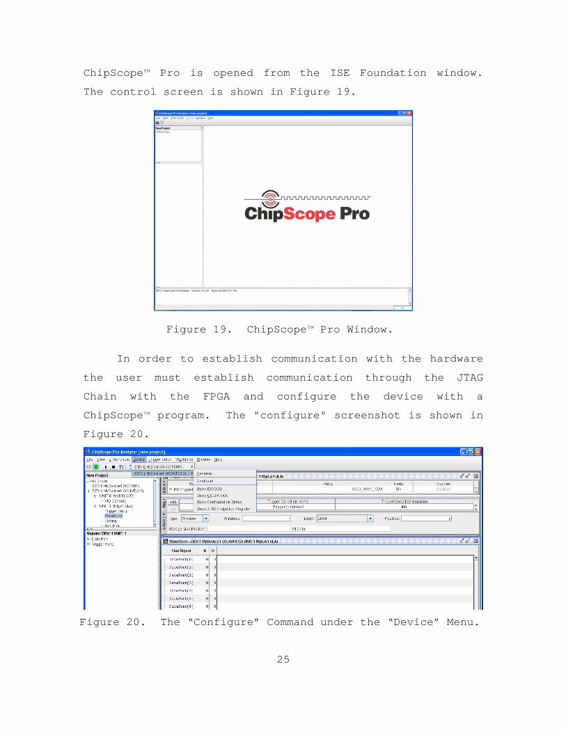
25
ChipScope™ Pro is opened from the ISE Foundation window.
The control screen is shown in Figure 19.
Figure 19. ChipScope™ Pro Window.
In order to establish communication with the hardware
the user must establish communication through the JTAG
Chain with the FPGA and configure the device with a
ChipScope™ program. The "configure" screenshot is shown in
Figure 20.
Figure 20. The “Configure” Command under the “Device” Menu.

26
The VIO Console allows the user to control the
hardware. For example, one bit can be toggled to turn the
converter on and off. The VIO Console is shown in Figure
21.
Figure 21. VIO Console in ChipScope™ Pro.
Now the user can remotely control the FPGA, and thus
the VSC digital control process, using ChipScope™ Pro;
hence, detailed analysis of input and output signals can be
accomplished digitally without instruments. The user can
evaluate a signal bit-by-bit if necessary, and calibration
of the sampled signal can be acommplished by simply
adjusting gain blocks in the Simulink® model. For this
power conversion laboratories, digital calibration is an
essential feature given that laboratory instruments are
often out of calibration. An example of digital calibration
will be expounded on in the next chapter.
E. CHAPTER SUMMARY
An overview of the hardware and software utilized in
the SDC was presented with a brief background of VSC
digital control. A thorough development of the SDC's CAD

27
process was offered as well. The next chapter covers the
design, construction, and testing of the analog signal
interface PCB and the power source interface PCB.

28
THIS PAGE INTENTIONALLY LEFT BLANK
29
III. PRINTED CIRCUIT BOARD DESIGN AND TESTING
A. SCHEMATIC LAYOUT AND PCB DESIGN
The main objective of this phase was to interface with
the Virtex-4TM Development Board and provide power to the
boards while maintaining signal clarity in the sampled
signals. PCB123 software was used to prepare the board
schematics for manufacture. A primary objective for the
design was the elimination of circuit interference, and a
thorough implementation of noise reduction techniques was
necessary to attain that objective. Signal decoupling,
shielding of tracks and proper ground plane layout were
critical to the success of the design. A summary of steps
taken to attain these goals is outlined below:
• A common-mode choke was used on the ribbon cable
connecting the analog and power PCBs.
• Snap grid and default track/pad sizes were chosen
to minimize signal loss and properly space key
components.
• Critical tracks were identified early so that
traces would not be routed too close to the
digital clock and other "noisy" components.
• All traces were kept as short as possible to
minimize signal loss and coupling.
• Active components drawing significant switching
current were “bypassed” using capacitors across
power rails. Capacitors were placed as close to
30
the desired component as possible. 22uF and 0.1uF
capacitors were used (depending on the voltage)
throughout the PCBs.
• A design rule check on the completed PCBs ensured
manufacturability, circuit connectivity, and
electrical clearance.
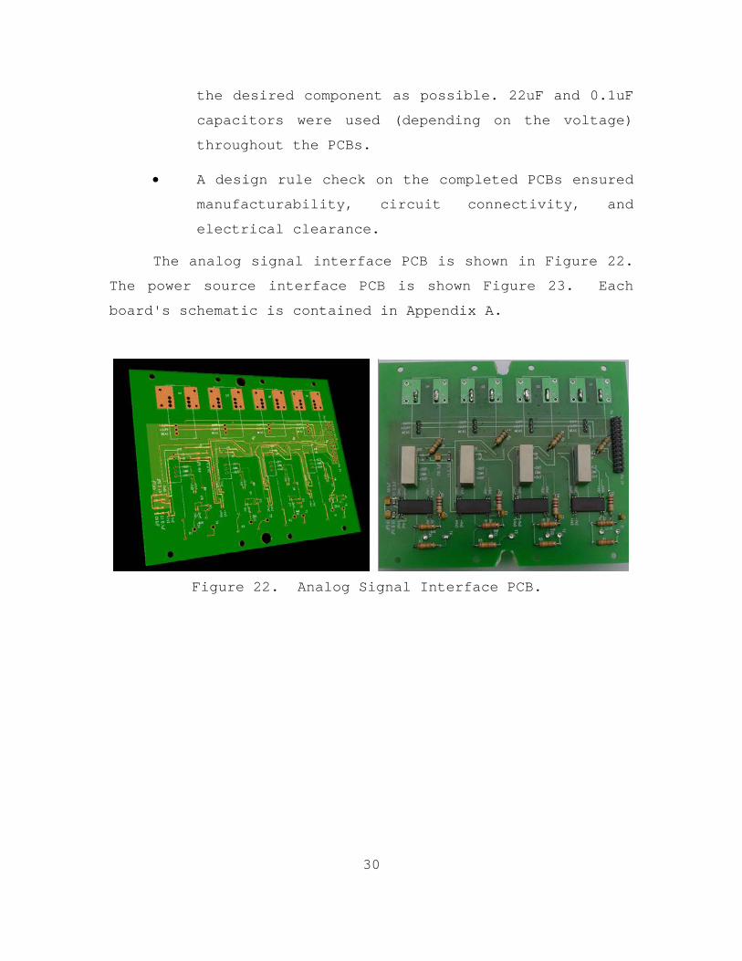
The analog signal interface PCB is shown in Figure 22.
The power source interface PCB is shown Figure 23. Each
board's schematic is contained in Appendix A.
Figure 22. Analog Signal Interface PCB.
31
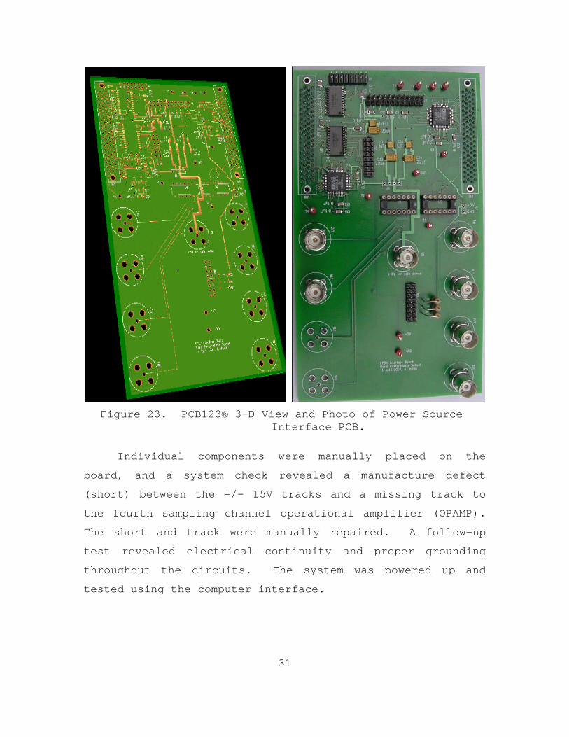
Figure 23. PCB123® 3-D View and Photo of Power Source
Interface PCB.
Individual components were manually placed on the
board, and a system check revealed a manufacture defect
(short) between the +/- 15V tracks and a missing track to
the fourth sampling channel operational amplifier (OPAMP).
The short and track were manually repaired. A follow-up
test revealed electrical continuity and proper grounding
throughout the circuits. The system was powered up and
tested using the computer interface.
32
B. MAJOR COMPONENT PACKAGING
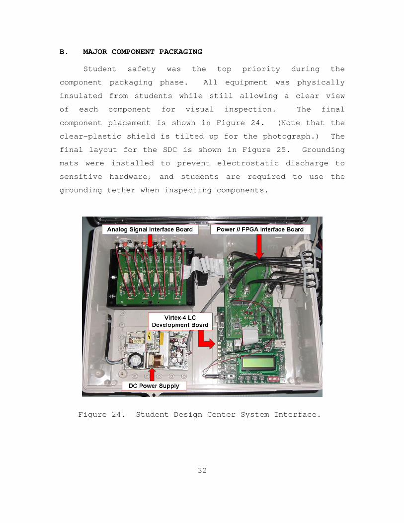
Student safety was the top priority during the
component packaging phase. All equipment was physically
insulated from students while still allowing a clear view
of each component for visual inspection. The final
component placement is shown in Figure 24. (Note that the
clear-plastic shield is tilted up for the photograph.) The
final layout for the SDC is shown in Figure 25. Grounding
mats were installed to prevent electrostatic discharge to
sensitive hardware, and students are required to use the
grounding tether when inspecting components.
Figure 24. Student Design Center System Interface.

33
Figure 25. Student Design Center.
C. ANALOG-DIGITAL CONVERSION OF FEEDBACK SIGNALS
The analog signal interface PCB contains four channels
to sample circuit voltages and four channels to sample
circuit currents. An AD-7864 analog-to-digital (A/D)
converter operating at a 500 kHz sampling rate was
dedicated to each set of channels. Sample-and-hold for
each channel was conducted in series for a total sampling
rate of 133kHz for each channel. This sampling rate was
more than sufficient to prevent aliasing when sampling low
frequency measurements typical for power electronics
laboratories. A diagram illustrating the conversion time
for each channel and the overall timing sequence is shown
in Figure 26.

34
Figure 26. Four Channel AD-7864 Timing Diagram [From [17]].
The measurements taken by the AD-7864s are displayed
in ChipScope™ Pro (or a standard oscilloscope) to enable
the detailed analysis of the signals. Sampled signals can
be calibrated precisely by adjusting the gain of the
feedback signals in the Simulink® model, thus enabling
accurate representation of physical samples. An example of
gain adjustment in Simulink® to enable digital calibration
is shown in Figure 27.
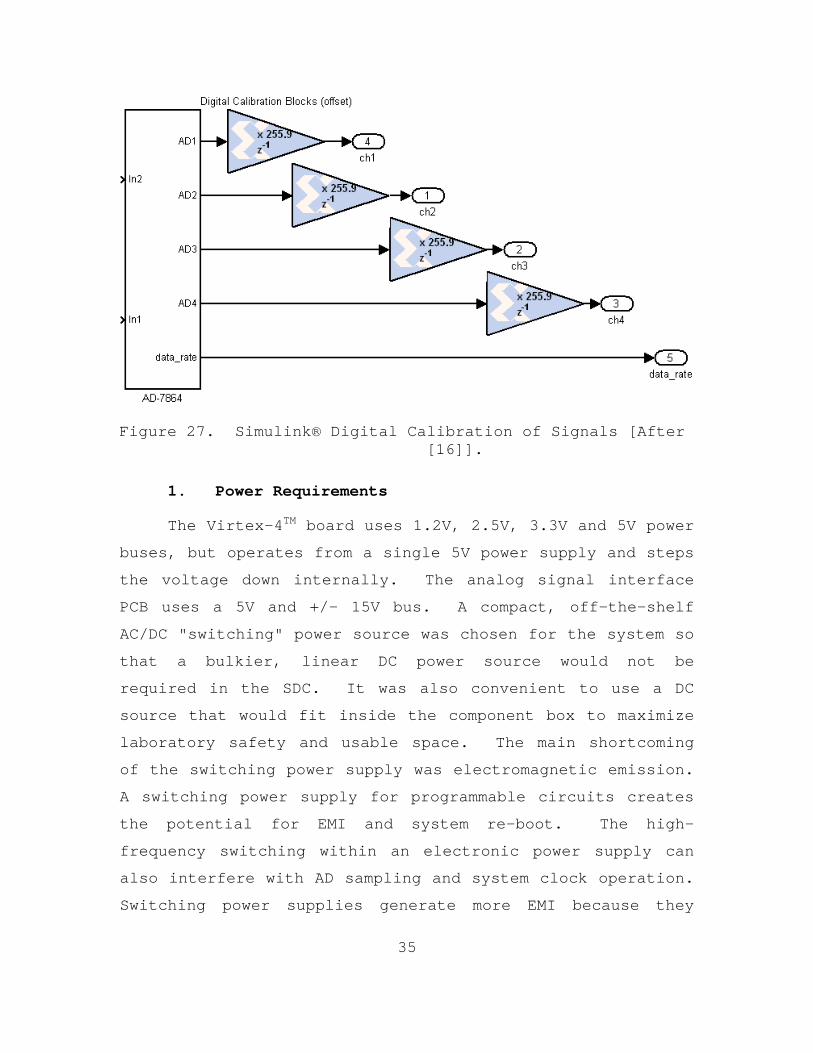
35
Figure 27. Simulink® Digital Calibration of Signals [After [16]].
1. Power Requirements
The Virtex-4TM board uses 1.2V, 2.5V, 3.3V and 5V power
buses, but operates from a single 5V power supply and steps
the voltage down internally. The analog signal interface
PCB uses a 5V and +/- 15V bus. A compact, off-the-shelf
AC/DC "switching" power source was chosen for the system so
that a bulkier, linear DC power source would not be
required in the SDC. It was also convenient to use a DC
source that would fit inside the component box to maximize
laboratory safety and usable space. The main shortcoming
of the switching power supply was electromagnetic emission.
A switching power supply for programmable circuits creates
the potential for EMI and system re-boot. The high-
frequency switching within an electronic power supply can
also interfere with AD sampling and system clock operation.
Switching power supplies generate more EMI because they
36
switch large currents at very high frequencies, anywhere
from 50 KHz to 1 MHz. At these high frequencies, optimal
power efficiencies and smaller components can be used in
the construction of the system which is why they are much
smaller than linear power sources. Because of its
efficiency and size, a switching power supply was the first
choice for the SDC [[18] and [19]].
To be certain that the power source did not interfere
with the circuit, a test of each of the eight channels was
conducted utilizing a linear power source (Tektronics PS280
DC power source) and a switching source to determine the
difference in noise levels. An analysis of signal output
showed no significant variation in signal noise due to the
switching source.
2. Conditioning of Sampled Signals
Although careful consideration was given to
implementing noise reduction techniques during PCB design
and construction and extensive testing was done using both
linear and switching power supplies, significant
interference from high frequency noise was observed in
ChipScope™ Pro during testing of the sampling channels.
Since the switching power supply was ruled out as the
primary source of noise in the preceding section, attention
was focused on the signal-to-noise ratio of the AD-7864
converters. For a 12 bit converter, noise + distortion is
in the range of 74dB, which is certainly enough to effect
distortion in the channels [17]; hence, there was good
reason to suspect that the AD converters were the source of
the noise observed in ChipScope™ Pro. Regardless of the
cause, a digital Low-Pass Filter (LPF) was utilized to

37
filter out the unwanted high-frequency interference. The
addition of a digital LPF into the Simulink® model was
easily achieved [[20] and [21]], and the SDC's software
foundation prevented the addition of a hardware LPF into
the design.
A cutoff frequency for the digital LPF was selected at
5kHz which was sufficient to pass all frequencies below
1kHz without significant attenuation. The 1kHz bandwidth
was adequate for SDC laboratories since it satisfied
frequency analysis requirement for all planned solid state
laboratories. To minimize the filter order and reduce
computational burden on the simulation software and the
FPGA, a large transition band was used. A 5kHz band
required only a 3rd order LPF for 20dB of attenuation in
the stop band. The derivation of the difference equation
coefficients for a symmetric Finite Impulse Response (FIR)
Butterworth filter is shown below.
24 MHz F = F =5 kHz s c170F =5-10kHz F =10kHzpassband stopband
T 2 (F )/ F c s1 1T 2 (F )/ Fsstopband2 2
⎛ ⎞⎜ ⎟⎜ ⎟⎜ ⎟⎜ ⎟⎜ ⎟⎜ ⎟ θ = ω = π⎜ ⎟
θ = ω = π⎜ ⎟⎜ ⎟⎝ ⎠
(2.12)
The prewarped analog frequencies are:
' '1 2tan tan1 22 2
θ θ⎛ ⎞ω = ω =⎜ ⎟
⎝ ⎠ (2.13)
' '1 2tan tan1 22 2
θ θ⎛ ⎞ω = ω =⎜ ⎟
⎝ ⎠ (2.14)

38
Translating the prewarped analog frequencies into a
normalized butterworth filter gives:
'
' 2 a1 '1
⎛ ⎞ω⎜ ⎟ω = ω ω =⎜ ⎟ω⎝ ⎠
(2.15)
Deriving the minimum butterworth filter order gives:
M /10dBN=[log(10 1)]/ 2 log( ) 2.58 3a
−⎛ ⎞− ω = ≈⎜ ⎟⎝ ⎠
(2.16)
Hence the transfer function for the normalized butterworth
filter is:
'1 '
1
s 3 2s ss
1H (s) H (s)LP LP s 2s s 1=
=ωω
⎡ ⎤⎡ ⎤= =⎣ ⎦ ⎢ ⎥+ + +⎣ ⎦ (2.17)
−⎡ ⎤=⎢ ⎥+⎣ ⎦
⎡ ⎤⎣ ⎦
z 1Utilizing the bilinear transform s , substituting
z 1
into H (s) , and deriving the difference equation gives:LP
H (z) H (s) z 1LP LP s z 10.2450e-6 x(n)+ 0.7349e-6 x(n 1)
+0.7349e-6 x(n-2) + 0.2450y(n 3)- 2.9749y(n 2)
+2.9500y(n 1) = 0.9752y(n)
⎛ ⎞⎡ ⎤= =−⎣ ⎦ =⎜ ⎟+⎜ ⎟−⎜ ⎟⎜ ⎟− −⎜ ⎟
−⎝ ⎠
(2.18)
The coefficients were verified using the Matlab
"maxflat" function, and the filter was integrated in the
simulation AD converter subsystem. The magnitude response
of the filter is shown in Figure 28. The filter subsystem
is shown in Figure 29.

39
0 0.01 0.02 0.03 0.04 0.05 0.06 0.07 0.08 0.09
-200
-180
-160
-140
-120
-100
-80
-60
-40
-20
0
Normalized Frequency (×π rad/sample)
Mag
nitu
de (d
B)
Magnitude Response (dB)
Figure 28. Lowpass Filter Magnitude Response.
Figure 29. Symmetric FIR Butterworth Filter [After [20]].
The results of the filter design were dramatic. A
comparison of a sampled three input signals (shown in blue)
at 1kHz, 5kHz and 10kHz and their filtered counterparts
(shown in green) are shown in Figure 30.

40
Figure 30. Original and Filtered 1kHz Signal.
Figure 31. Original and Filtered 5kHz Signal.
Figure 32. Original and Filtered 10kHz Signal.
41
Excellent attenuation was shown as the frequency
approached the stop band and virtually all high-frequency
interference was blocked.
D. CHAPTER SUMMARY
This chapter covered the analog signal interface PCB
and the power source interface PCB design, construction and
testing. An overview of why a switching power source was
used in the SDC and techniques used to troubleshoot and
reduce system noise was presented. Finally, a digital LPF
was developed and implemented to eliminate EMI. Chapter
III summarizes this thesis and presents topics for future
research.

42
THIS PAGE INTENTIONALLY LEFT BLANK

43
IV. CONCLUSIONS AND RECOMMENDATIONS
A. SUMMARY
This thesis began with an overview of the SDC
objectives and descriptions of the hardware and software
used therein. The purpose and function of each component
was explained in order to develop a working knowledge of
SDC capabilities. Standard operating procedures were
developed to serve as a working document for future
students conducting laboratories in the SDC and to provide
them with a better understanding of design flow prior to
execution. The thesis expounded on the design and testing
of the interface PCBs and system performance testing was
done to ensure EMI from the switching power supply did not
inhibit signal sampling. Finally, a lowpass filter was
designed and implemented to reduce the high frequency
interference on the channel signals noted in ChipScope™ Pro
during testing.
B. CONCLUSIONS
The SDC is an excellent resource for digital control
of power electronics design. Students gain a fundamental
understanding of the advantages of FPGA digital control of
power systems and digital signal analysis using ChipScope™
Pro. The SDC enables students to make accurate predictions
of component behavior using software simulation and testing
to verify results. The SDC can be adapted as necessary to
changing technology due to its flexible FPGA foundation.
New programs and ideas can be implemented without changing
hardware and increasing cost. Moreover, as noted in Chapter
I, the SDC is not limited to power electronics design and
44
control. Since three systems are available, students in
other curriculums can explore the potential of FPGA design
and control of other electrical systems.
C. RECOMMENDATIONS FOR FURTHER RESEARCH
There are many opportunities for research in the area
of FPGA digital control of power electronics. Below are
three ideas to serve as platforms for further research:
• Development of FPGA laboratories for other
electrical engineering curriculum tracks.
• Redundant FPGA control of power electronics in
order to improve system reliability.
• Design and Implementation of FPGA "soft-radio"
systems.
The reprogrammable nature of the FPGA hardware enables
a large number of programs and systems to be explored
without the burden of purchasing and installing new
hardware; hence, electrical engineering design, especially
at the graduate level, can benefit greatly from the use of
FPGA technology.
45
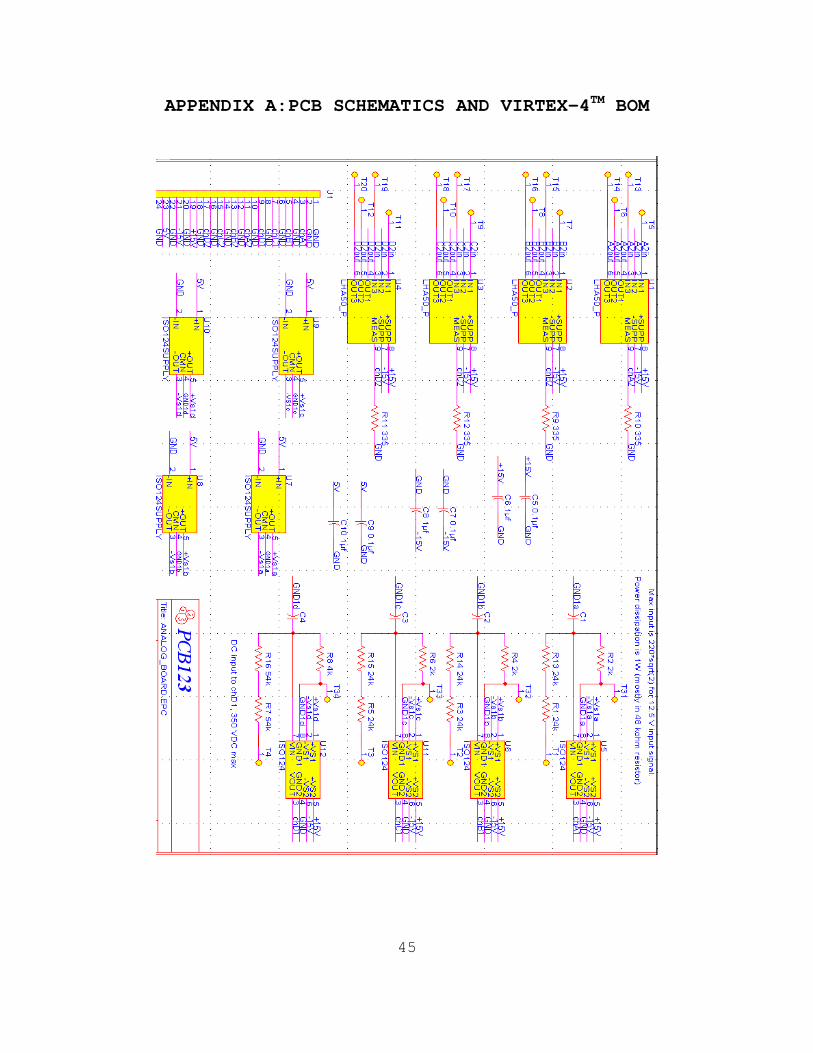
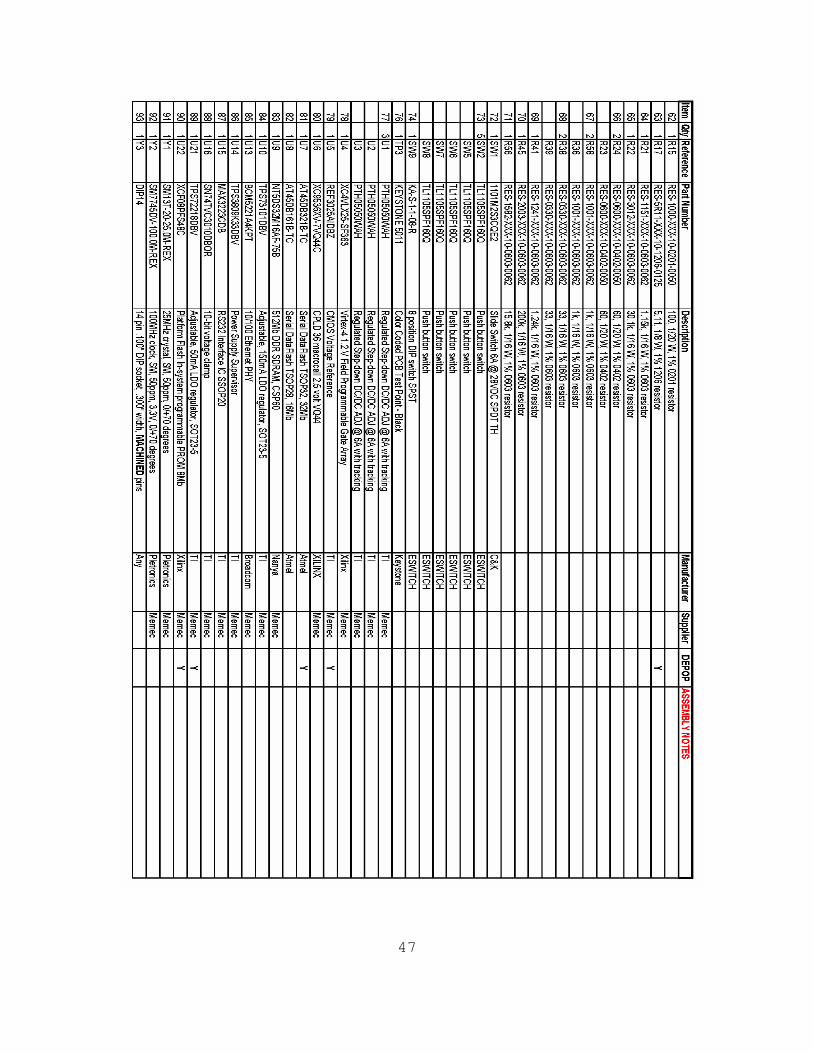
APPENDIX A: PCB SCHEMATICS AND VIRTEX-4TM BOM

46
47
48

49
50

51

52
53
APPENDIX B: VIRTEX-4TM CONDENSED USER'S GUIDE
A. VIRTEX-4TM DEVELOPMENT BOARD COMPONENTS
All figures and information in this appendix were
excerpted verbatim from the Virtex-4™ LC Development Board
user's guide. Figure numbers were changed to correspond
with this thesis.
1. DDR SDRAM
The Virtex-4™ LC Development Board provides 64MB of
DDR SDRAM memory (32Mx16). A high-level block diagram of
the DDR SDRAM interface is shown below.
Figure 33. DDR SDRAM Interface.
2. Clock Sources
The clock generation section of the Virtex-4™ LC
Development Board provides all necessary clock for the I/O
devices located on the board as well as the DDR SDRAM
memory. An on-board 100MHz oscillator provides the system
clock input to the FPGA. In addition to the above clock
input, a socket is provided on the board that can be used
54
to provide a single-ended LVTTL clock input to the FPGA via
an 8 or 4-pin oscillator. The following figure shows the
clock.
Figure 34. Clock Sources on the Virtex-4™ board.
3. 10/100 Ethernet PHY
The Virtex-4™ LC Development Board provides a 10/100
Ethernet port for network connection. A high-level block
diagram of the 10/100 Ethernet interface is shown in the
figure below.
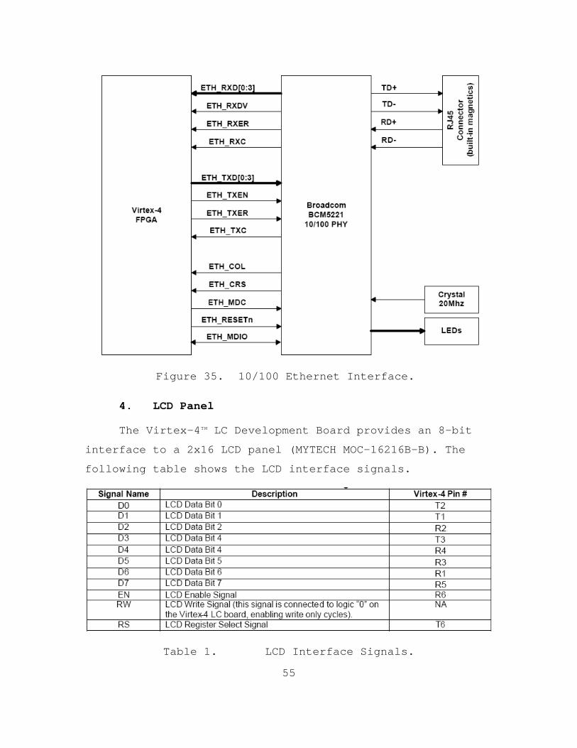
55
Figure 35. 10/100 Ethernet Interface.
4. LCD Panel
The Virtex-4™ LC Development Board provides an 8-bit
interface to a 2x16 LCD panel (MYTECH MOC-16216B-B). The
following table shows the LCD interface signals.
Table 1. LCD Interface Signals.

56
5. RS232 Interface
The Virtex-4™ LC Development Board provides an RS232
interface with RX and TX signals and jumpers for connecting
the RTS and CTS signals. The following figure shows the
RS232 interface to the Virtex-4™ LX25 FPGA.
Figure 36. RS232 Interface.
6. User DIP and PB Switches
The Virtex-4™ LC Development Board provides four user
push button switches as described in the following table.
An active low signal is generated when a given switch is
pressed.
Table 2. Push Button Switch Pin Assignments.

57
The Virtex-4™ LC Development Board provides an 8-
position DIP switch as described in the following table. An
active low signal is generated when a given switch is ON.
Table 3. DIP Switch Pin Assignments.
7. User LEDs
The Virtex-4™ LC Development Board provides four user
LEDs that can be turned “ON” by driving the LEDx signal to
a logic “0”. The following table shows the user LEDs and
their associated FPGA pin assignments.
Table 4. LED Pin Assignments.
8. User GPIO
The Virtex-4™ LC Development Board provides a general-
purpose GPIO header (JP26) that consists of 6 user signals,
a 3.3V power pin and a ground pin. The following table
shows the GPIO pin assignments.
58
Table 5. GPIO Pin Assignments.
9. Configuration and Debug Ports
Various methods of configuration and debug support are
provided on the Virtex-4™ LC Development Board to assist
designers during testing and debugging of their
applications. The following sections provide brief
descriptions of each of these interfaces.
a. JTAG Gain
The following figure shows the JTAG chain on the
Virtex-4™ LC Development Board. The XC9536XV along with a
serial data flash is used to configure the FPGA.
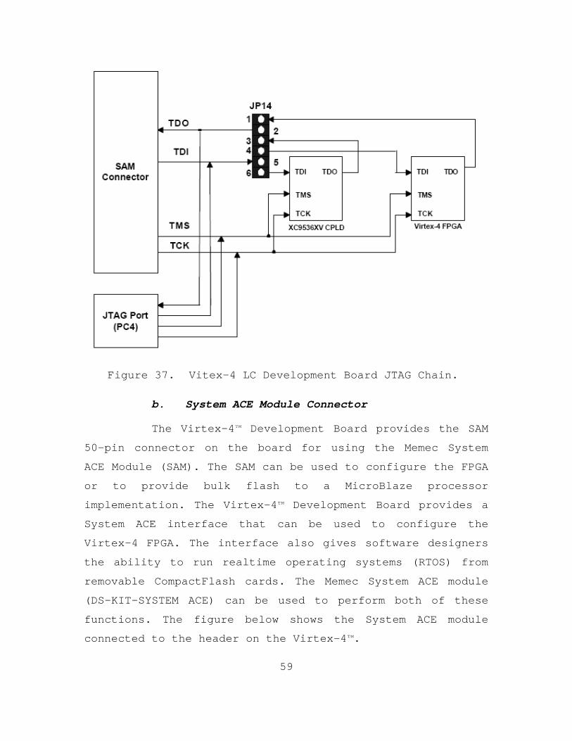
59
Figure 37. Vitex-4 LC Development Board JTAG Chain.
b. System ACE Module Connector
The Virtex-4™ Development Board provides the SAM
50-pin connector on the board for using the Memec System
ACE Module (SAM). The SAM can be used to configure the FPGA
or to provide bulk flash to a MicroBlaze processor
implementation. The Virtex-4™ Development Board provides a
System ACE interface that can be used to configure the
Virtex-4 FPGA. The interface also gives software designers
the ability to run realtime operating systems (RTOS) from
removable CompactFlash cards. The Memec System ACE module
(DS-KIT-SYSTEM ACE) can be used to perform both of these
functions. The figure below shows the System ACE module
connected to the header on the Virtex-4™.
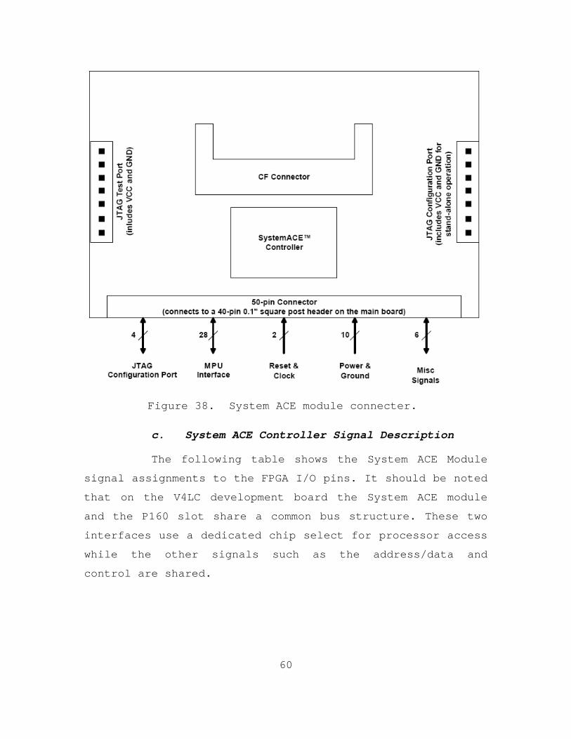
60
Figure 38. System ACE module connecter.
c. System ACE Controller Signal Description
The following table shows the System ACE Module
signal assignments to the FPGA I/O pins. It should be noted
that on the V4LC development board the System ACE module
and the P160 slot share a common bus structure. These two
interfaces use a dedicated chip select for processor access
while the other signals such as the address/data and
control are shared.
61
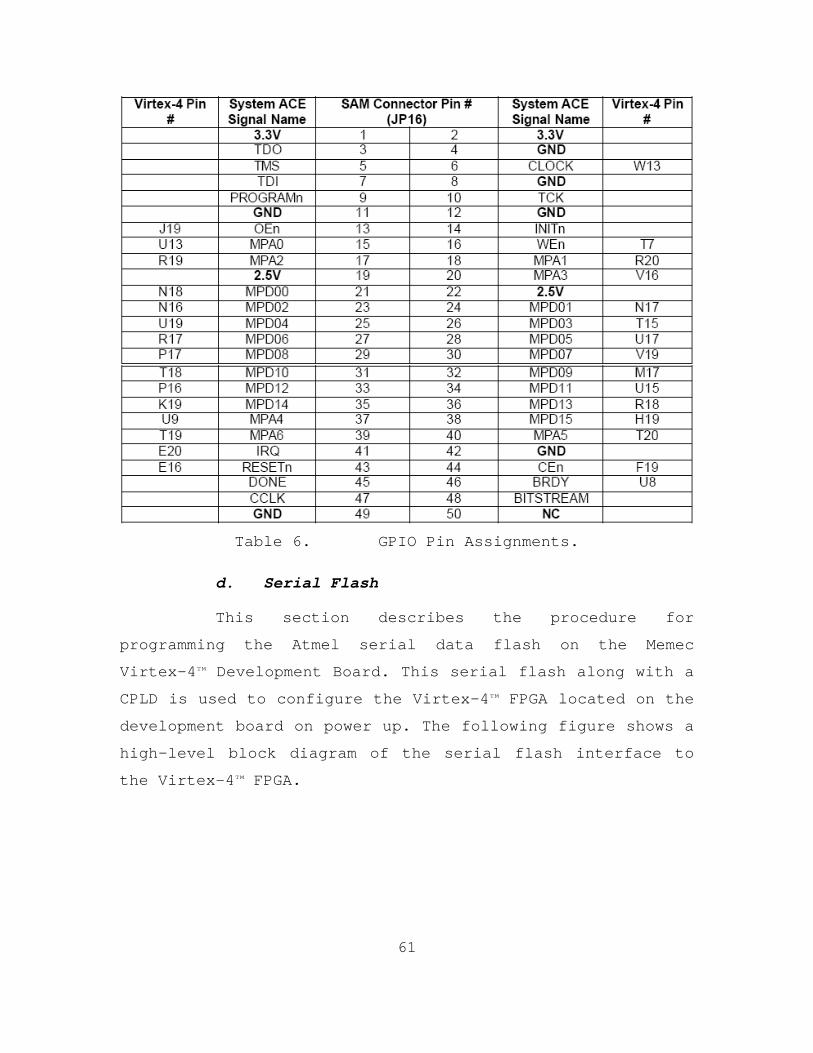
Table 6. GPIO Pin Assignments.
d. Serial Flash
This section describes the procedure for
programming the Atmel serial data flash on the Memec
Virtex-4™ Development Board. This serial flash along with a
CPLD is used to configure the Virtex-4™ FPGA located on the
development board on power up. The following figure shows a
high-level block diagram of the serial flash interface to
the Virtex-4™ FPGA.
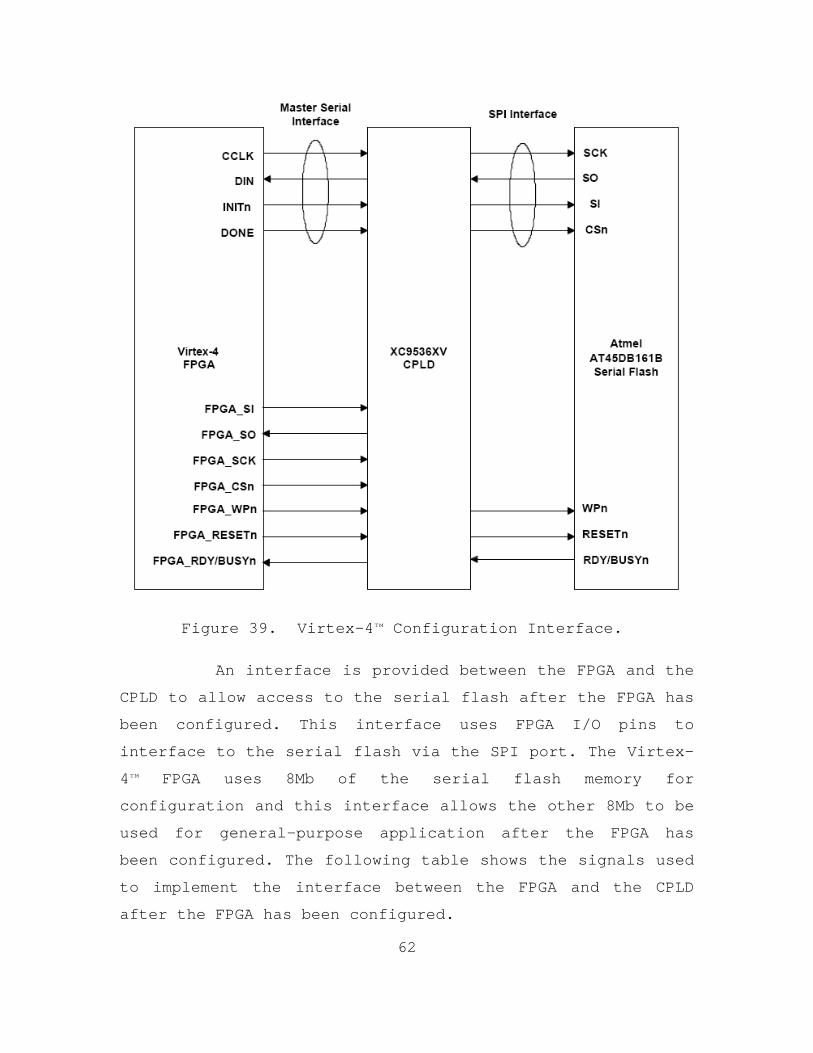
62
Figure 39. Virtex-4™ Configuration Interface.
An interface is provided between the FPGA and the
CPLD to allow access to the serial flash after the FPGA has
been configured. This interface uses FPGA I/O pins to
interface to the serial flash via the SPI port. The Virtex-
4™ FPGA uses 8Mb of the serial flash memory for
configuration and this interface allows the other 8Mb to be
used for general-purpose application after the FPGA has
been configured. The following table shows the signals used
to implement the interface between the FPGA and the CPLD
after the FPGA has been configured.

63
Table 7. FPGA SPI Interface Pin Assignments.
The primary function of the CPLD is to translate
the Master Serial interface to the SPI interface of the
serial flash. The XC9536XV CPLD uses the FPGA CCLK clock
along with the INITn and DONE signals to drive the SPI SI,
SCK and CSn signals. The SO output of the serial flash is
used by the CPLD to drive the DIN signal of the FPGA.
e. JTAG Chain on the Virtex-4™ Development Board
The following figure shows the JTAG chain on the
Virtex-4™ Development Board. As mentioned, the CPLD is used
for interfacing to the configuration flash and does not
provide any user logic. Hence, this CPLD is programmed by
Memec prior to shipping the board. The programming file for
the CPLD is provided in case re-programming of the CPLD
becomes necessary. The CPLD must be programmed prior to
performing any operations on the serial flash such as
erasing, programming, reading or verifying.

64
Figure 40. Virtex-4™ Development Board JTAG Chain.
The following table shows jumper settings for the
JTAG chain on the Virtex-4™ Development Board.
Table 8. JTAG Chain Jumper Settings.
f. Configuration Flash on the Virtex-4™ Development Board
The following figure shows the detail of the
interface between the FPGA and the serial flash. A PC4
cable is used to program the serial flash with the FPGA
bitstream. Once the flash is programmed, on power-up, the
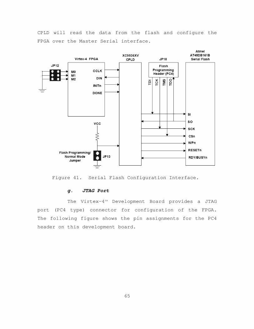
65
CPLD will read the data from the flash and configure the
FPGA over the Master Serial interface.
Figure 41. Serial Flash Configuration Interface.
g. JTAG Port
The Virtex-4™ Development Board provides a JTAG
port (PC4 type) connector for configuration of the FPGA.
The following figure shows the pin assignments for the PC4
header on this development board.

66
Figure 42. PC4 JTAG Port Connector.
h. Configuration Modes
The following table shows the Virtex-4™
Development Board configuration modes.
Table 9. FPGA Configuration Mode Jumper Settings.
10. Voltage Regulators
The following figure shows the voltage regulators that
are used on Virtex-4™ Development Board to provide various
on-board voltage sources. As shown in the following figure,
a connector is used to provide the main 5.0V voltage to the
board. This voltage source is provided to all onboard
regulators to generate the 1.2V, 2.5V, and 3.3V voltages.
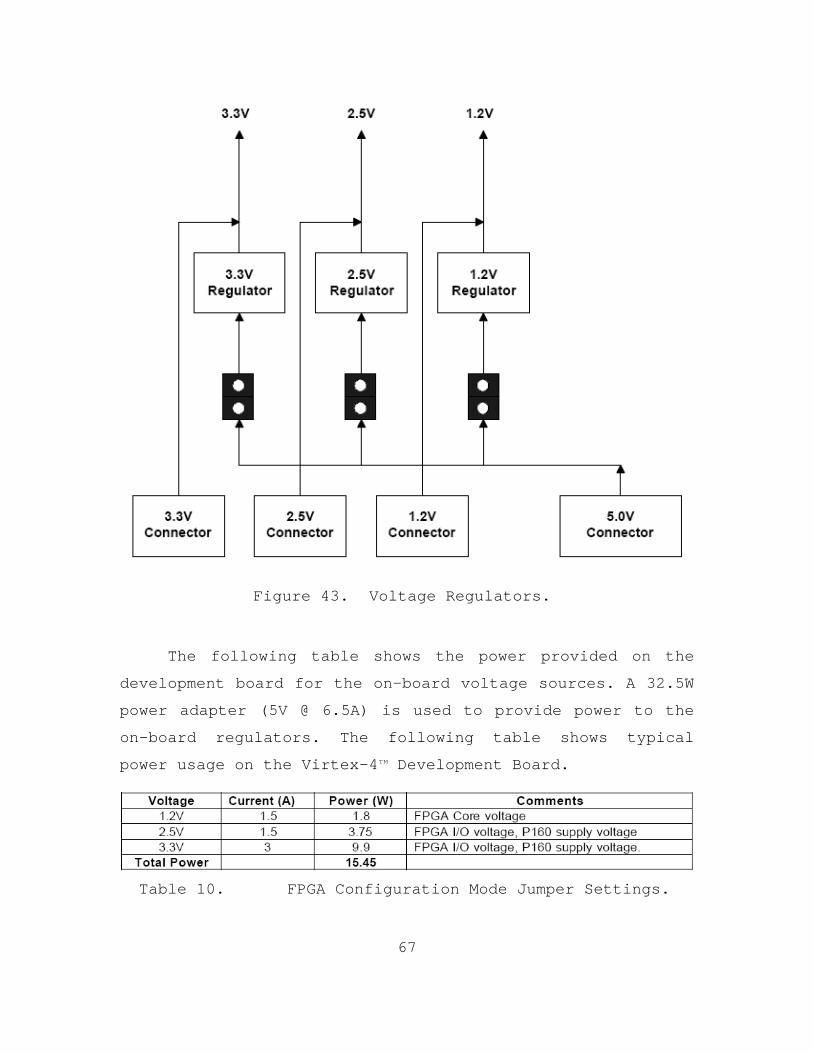
67
Figure 43. Voltage Regulators.
The following table shows the power provided on the
development board for the on-board voltage sources. A 32.5W
power adapter (5V @ 6.5A) is used to provide power to the
on-board regulators. The following table shows typical
power usage on the Virtex-4™ Development Board.
Table 10. FPGA Configuration Mode Jumper Settings.

68
If the current provided by the on-board regulator is
not sufficient for some applications, the user can directly
drive the voltage source and bypass the on-board
regulators.
11. Bank I/O Voltage
The following table shows the Virtex-4™ Development
Board bank I/O voltages on the Virtex-4™ Development Board.
Table 11. I/O Bank Voltages.
12. P160 Expansion Module Signal Assignments
The following tables show the Virtex-4™ pin
assignments to the P160 Expansion Module connectors (JX1 &
JX2) located on the Virtex-4™ Development Board.
69
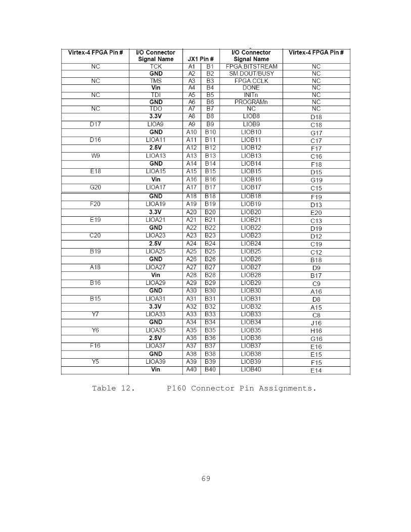
Table 12. P160 Connector Pin Assignments.

70
Table 13. P160 Connector Pin Assignments.
71
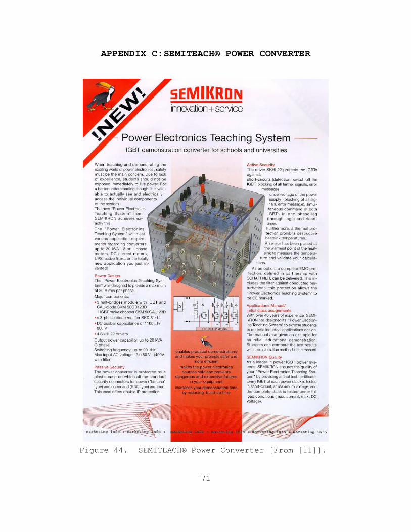
APPENDIX C: SEMITEACH® POWER CONVERTER
Figure 44. SEMITEACH® Power Converter [From [11]].

72
THIS PAGE INTENTIONALLY LEFT BLANK
73
LIST OF REFERENCES
[1] J. Schneider, M. Bezdek, Z. Zhang, Z. Zhang, and D. Rover, "A Platform FPGA-based Hardware-Software Undergraduate Laboratory," Presented at the IEEE International Conference on Microelectronic Systems Education, 2005.
[2] J. Lund, “Field programmable gate array hysteresis
control of parallel connected inverters,” M.S. thesis, Naval Postgraduate School, Monterey, California, 2006.
[3] D. Jackson and K. Ricks, "FPGA-Based Autonomous
Vehicle Competitions in a Capstone Design Course," Presented at the IEEE International Conference on Microelectronic Systems Education, 2005.
[4] C. Quintans, M. Valdes, M. Moure, L. Fernandez-
Ferreira and E. Mandado, "Digital Electronics Learning System Based on FPGA Applications," Presented at the 35th ASEE/IEEE Frontiers in Education Conference, Indianapolis, October 2005.
[5] S. Brown and J. Rose, Architecture of FPGAs and CPLDs:
A tutorial, Department of Electrical and Computer Engineering, University of Toronto, 1995.
[6] Wikipedia®, “Field programmable gate arrays,”
http://en.wikipedia.org/wiki/FPGA, last visited 11 April 2007.
[7] A. Julian, Notes for EC4130 (Advanced Electrical
Machinery Systems), Naval Postgraduate School, Monterey, California, 2007 (unpublished).
[8] XILINX® Products and Services, "The DSP Primer 1,"
http://www.xilinx.com/univ/downld_partnerteaching.htm, last visited 15 August 2007.
[9] MEMECTM corporation technical staff, Virtex-4™ LC
Development Board User’s Guide Version 2.0, MEMECTM Corporation, 2005.
74
[10] XILINX® Products and Services, "Basic FPGA Architecture and ChipScope™ Pro," http://www.xilinx.com/univ/downld_partnerteaching.htm http://www.xilinx.com/ise/optional_prod/cspro.htm, last visited 15 August 2007.
[11] Semikron® Products Marketing Information, "Power
electronics systems (SEMISTACK)," http://www.semikron.com/internet/index.jsp?sekId=361, last visited 15 August 2007.
[12] A. Julian, Notes for EC4150 (Advanced Solid State
Power Conversion), Naval Postgraduate School, Monterey, California, 2007 (unpublished).
[13] P.Krause, O. Wasynczuk, and S. Sudhoff, Analysis of
Electric Machinery and Drive Systems, 2nd Edition, pp. 506-510, IEEE Press, New York, 2002.
[14] Mathworks Product Marketing Information, " Simulink® -
simulation and model-based design," http://www.mathworks.com/products/simulink/?BB=1, last visited 15 August 2007.
[15] A. Julian, Notes for EC3150 (Solid State Power
Conversion) Laboratory 1: Power Electronics Lab Tools Familiarization, Naval Postgraduate School, Monterey, California, 2007 (unpublished).
[16] A. Julian, Notes for EC3150 (Solid State Power
Conversion) Laboratory 2: Buck Converter with Regeneration, Naval Postgraduate School, Monterey, California, 2007 (unpublished).
[17] Analog Devices, "AD7864 Specifications,"
http://www.analogdevices.com, last visited 15 August 2007.
[18] Medical Electronics Manufacturing, "EMI considerations
in selecting AC/DC switching power supplies," http://www.devicelink.com/mem/archive/05/10/007.html, last visited 15 August 2007.
[19] N. Mohan, T. Undeland, and W. Robbins, Power
Electronics, 3rd Edition, pp. 301-304, John Wiley and Sons, Inc, New Jersey, 2003.

75
[20] A. Julian, private conversation at Naval Postgraduate School, December 2007.
[21] R. Strum and D. Kirk, First Principles of Discrete
Systems and Digital Signal Processing, 1st Edition, pp. 623-629, Addison-Wesley Publishing Company, Inc, New York, 1989.

76
THIS PAGE INTENTIONALLY LEFT BLANK

77
INITIAL DISTRIBUTION LIST
1. Defense Technical Information Center Ft. Belvoir, Virginia
2. Dudley Knox Library Naval Postgraduate School Monterey, California
3. Dr. Jeffrey Knorr Electrical Engineering and Computer Department Code EC/Ko Naval Postgraduate School Monterey, California
4. Dr. Alexander Julian Electrical Engineering and Computer Department Code EC/J1 Naval Postgraduate School Monterey, California
5. Dr. Roberto Cristi Electrical Engineering and Computer Department Code EC/C1 Naval Postgraduate School Monterey, California
6. Marine Corps Representative Naval Postgraduate School Monterey, California 7. Director, Training and Education, MCCDC, Code C46 Quantico, Virginia 8. Director, Marine Corps Research Center, MCCDC, Code C40RC Quantico, Virginia 9. Marine Corps Tactical Systems Support Activity (Attn: Operations Officer) Camp Pendleton, California