naval postgraduate school - defense technical …dtic.mil/dtic/tr/fulltext/u2/a435676.pdf · tested...
TRANSCRIPT
NAVAL
POSTGRADUATE SCHOOL
MONTEREY, CALIFORNIA
THESIS
CLOSED LOOP CONTROL OF A CASCADED MULTI-LEVEL CONVERTER TO MINIMIZE HARMONIC DISTORTION
by
Brian E. Souhan
June 2005
Thesis Advisor: Robert W. Ashton Second Reader: Alexander Julian
Approved for public release; distribution is unlimited

THIS PAGE INTENTIONALLY LEFT BLANK

i
REPORT DOCUMENTATION PAGE Form Approved OMB No. 0704-0188 Public reporting burden for this collection of information is estimated to average 1 hour per response, including the time for reviewing instruction, searching existing data sources, gathering and maintaining the data needed, and completing and reviewing the collection of information. Send comments regarding this burden estimate or any other aspect of this collection of information, including suggestions for reducing this burden, to Washington headquarters Services, Directorate for Information Operations and Reports, 1215 Jefferson Davis Highway, Suite 1204, Arlington, VA 22202-4302, and to the Office of Management and Budget, Paperwork Reduction Project (0704-0188) Washington DC 20503. 1. AGENCY USE ONLY (Leave blank)
2. REPORT DATE June 2005
3. REPORT TYPE AND DATES COVERED Master’s Thesis
4. TITLE AND SUBTITLE: Closed Loop Control of a Cascaded Multi-Level Converter to Minimize Harmonic Distortion
6. AUTHOR(S) Brian E. Souhan
5. FUNDING NUMBERS
7. PERFORMING ORGANIZATION NAME(S) AND ADDRESS(ES) Naval Postgraduate School Monterey, CA 93943-5000
8. PERFORMING ORGANIZATION REPORT NUMBER
9. SPONSORING /MONITORING AGENCY NAME(S) AND ADDRESS(ES) N/A
10. SPONSORING/MONITORING AGENCY REPORT NUMBER
11. SUPPLEMENTARY NOTES The views expressed in this thesis are those of the author and do not reflect the official policy or position of the Department of Defense or the U.S. Government. 12a. DISTRIBUTION / AVAILABILITY STATEMENT Approved for public release; distribution is unlimited
12b. DISTRIBUTION CODE
13. ABSTRACT (maximum 200 words)
As the United States Navy moves toward the all-electric ship, the need for a robust, high fidelity inverter for propulsion motors becomes mandatory. Military vessels require high power converters capable of producing nearly sinusoidal outputs to prevent torque pulsations and electrical noise that can compromise the mission location. This thesis presents a hybrid pulse-width-modulated controller for a 3x3 Cascaded Multi-Level Converter (CMLC). Ancil-lary results include a simple technique for extracting the reference sine wave from an inde-pendent bulk converter and implementing a synchronization technique that coordinates a space vector modulation controller with the switching pattern of a bulk inverter. The algorithms were tested on CMLC hardware that resides in the Naval Postgraduate School Power Systems Labo-ratory, and the results were compared with a sine-triangle pulse width modulation algorithm. The controller and converter were used to power a quarter-horsepower three-phase induction motor.
15. NUMBER OF PAGES
105
14. SUBJECT TERMS Cascaded Multi-Level Converter, Space Vector Modulation, Sine-Triangle Pulse Width Modulation, Neutral Point Clamped, Digital Phase-Locked Loop, Uncoupled Control, DD(X), dSPACE, Integrated Power System, All Electric Ship, Electric Propulsion.
16. PRICE CODE
17. SECURITY CLASSIFICATION OF REPORT
Unclassified
18. SECURITY CLASSIFICATION OF THIS PAGE
Unclassified
19. SECURITY CLASSIFICATION OF ABSTRACT
Unclassified
20. LIMITATION OF ABSTRACT
UL
NSN 7540-01-280-5500 Standard Form 298 (Rev. 2-89) Prescribed by ANSI Std. 239-18

ii
THIS PAGE INTENTIONALLY LEFT BLANK
iii
Approved for public release; distribution is unlimited
CLOSED LOOP CONTROL OF A CASCADED MULTI-LEVEL CONVERTER TO MINIMIZE HARMONIC DISTORTION
Brian E. Souhan
Captain, United States Army B.S., University of Cincinnati, 1997
Submitted in partial fulfillment of the requirements for the degree of
MASTER OF SCIENCE IN ELECTRICAL ENGINEERING
from the
NAVAL POSTGRADUATE SCHOOL June 2005
Author: Brian E. Souhan
Approved by: Robert W. Ashton
Thesis Advisor
Alexander Julian Second Reader
John P. Powers Chairman, Department of Electrical and Computer Engineering

iv
THIS PAGE INTENTIONALLY LEFT BLANK

v
ABSTRACT As the United States Navy moves toward the all-electric ship, the need for a ro-
bust, high fidelity inverter for propulsion motors becomes mandatory. Military vessels
require high power converters capable of producing nearly sinusoidal outputs to prevent
torque pulsations and electrical noise that can compromise the mission location. This
thesis presents a hybrid pulse-width-modulated controller for a 3x3 Cascaded Multi-
Level Converter (CMLC). Ancillary results include a simple technique for extracting the
reference sine wave from an independent bulk converter and implementing a synchroni-
zation technique that coordinates a space vector modulation controller with the switching
pattern of a bulk inverter. The algorithms were tested on CMLC hardware that resides in
the Naval Postgraduate School Power Systems Laboratory, and the results were com-
pared with a sine-triangle pulse width modulation algorithm. The controller and con-
verter testing was done on a quarter-horsepower three-phase induction motor.

vi
THIS PAGE INTENTIONALLY LEFT BLANK
vii
TABLE OF CONTENTS
I. INTRODUCTION........................................................................................................1 A. NAVAL POWER .............................................................................................1 B. PROPULSION REQUIREMENTS ...............................................................3
1. Stealth....................................................................................................4 2. Space......................................................................................................4 3. Cost........................................................................................................5 4. Reliability and Maintenance. ..............................................................5
C. PROPULSION SYSTEMS..............................................................................6 D. THESIS GOAL ................................................................................................7 E. THESIS OVERVIEW .....................................................................................7
II. INVERTERS ................................................................................................................9 A. OVERVIEW.....................................................................................................9 B. INVERTER TOPOLOGIES...........................................................................9 C. CONTROL ALGORITHMS FOR INVERTERS ......................................14 D. NPS-BUILT 3X3 NEUTRAL-POINT CLAMPED CASCADED
MULTI-LEVEL CONVERTER...................................................................15 1. Hardware ............................................................................................15 2. DSP Controller ...................................................................................16 3. Control Algorithm .............................................................................18
E. SUMMARY ....................................................................................................20
III. UNCOUPLED CONTROL.......................................................................................21 A. OVERVIEW...................................................................................................21 B. UNCOUPLED CONTROL...........................................................................21 C. BULK INVERTER OPERATION...............................................................24 D. DIGITAL SPIKE ELIMINATION..............................................................29 E. SUMMARY ....................................................................................................31
IV. SPACE VECTOR MODULATION.........................................................................33 A. OVERVIEW...................................................................................................33 B. SPACE VECTOR MODULATION.............................................................33 C. SPACE VECTOR MODULATION IN THE q-d REFERENCE
FRAME...........................................................................................................34 1. Transform into the q-d Reference Frame ........................................34 2. Detection of Three Nearest Vectors..................................................35 3. Determination of the Duty Cycle ......................................................36 4. Transform into Relevant Switching States ......................................37
D. SPACE VECTOR MODULATION g-h REFERENCE FRAME.............38 1. Transformation to g-h Reference Frame.........................................38 2. Determination of Three Nearest Vectors.........................................39 3. Determination of the Duty Cycle ......................................................40 4. Transform Into Relevant Switching States......................................40

viii
E. HYBRID ALGORITHM...............................................................................41 F. SUMMARY ....................................................................................................42
V. IMPLEMENTATION OF ALGORITHMS............................................................43 A. OVERVIEW...................................................................................................43 B. BULK CONVERTER CONTROLLER ......................................................43
1. Bulk Converter...................................................................................43 2. Reference Sine Wave Generation.....................................................44
C. CONDITIONING CONTROLLER CONVERTER ..................................48 1. SVM Algorithm..................................................................................49 2. Hybrid Algorithm ..............................................................................55
D. HARDWARE INTERFACE.........................................................................58 1. Hardware Communications..............................................................58 2. Hardware Simulation ........................................................................61
E. SUMMARY ....................................................................................................62
VI. RESULTS ...................................................................................................................63 A. OVERVIEW...................................................................................................63 B. SIMULATIONS .............................................................................................64
1. SVM Simulations ...............................................................................64 2. Hybrid Algorithm Simulations .........................................................68
C. HARDWARE RESULTS ..............................................................................69 1. SVM Hardware Tests ........................................................................71 2. Hybrid Algorithm Hardware Results ..............................................74
D. COMPARISON WITH SPWM ALGORITHM .........................................76 E. SUMMARY...........................................................................................................78
VII. CONCLUSIONS ........................................................................................................81 A. SUMMARY OF FINDINGS .........................................................................81 B. FUTURE WORK...........................................................................................82
LIST OF REFERENCES......................................................................................................83
INITIAL DISTRIBUTION LIST .........................................................................................85

ix
LIST OF FIGURES
Figure 1. Electric Power Generating Capacity [From Ref. 3.]..........................................2 Figure 2. Propulsion Power Requirements vs. Speed [From Ref. 3.] ...............................3 Figure 3. ALSTOM 20MW Azimuth Pod (MermaidTM) [From Ref. 4.] ..........................4 Figure 4. Propulsion System Block Diagram....................................................................6 Figure 5. Single-Phase H-bridge Voltage Source Inverter................................................9 Figure 6. Two-Level Three-Phase Voltage Source Inverter ...........................................10 Figure 7. Three-Level Three-Phase NPC Voltage Source Inverter [From Ref. 7.] ........11 Figure 8. 3x3 Cascaded Multi-Level Converter [From Ref. 7.]......................................12 Figure 9. Vector Plots for Different Voltage Ratios [After Ref. 2.]................................14 Figure 10. Layout of Single Converter [From Ref. 7.]......................................................16 Figure 11. DS1103 PPC Controller Board [From Ref. 13.] ..............................................17 Figure 12. CP1103 I/O Board [From Ref. 14.] .................................................................18 Figure 13. Sine Triangle Waveform [From Ref. 7.]..........................................................19 Figure 14. Cascaded Multi-Level Inverter [From Ref. 7.] ................................................22 Figure 15. Bulk Converter Output With Reference Sine Wave ........................................23 Figure 16. Harmonic Waveform for Phase A [After Ref. 2.]............................................24 Figure 17. Bulk Inverter Output Waveform [After Ref. 2.] ..............................................25 Figure 18. Available Switching States for α = 0º..............................................................26 Figure 19. Available Switching States for α = 15° ...........................................................26 Figure 20. Available Switching States for α = 45° ...........................................................27 Figure 21. Block Diagram for q-d Reference Sine Wave Generation [After Ref. 6.].......28 Figure 22. Simulation Showing Spikes Produced in Output Waveform...........................30 Figure 23. q-d Transform of a Three-Phase Voltage Source ...........................................34 Figure 24. SVM Plot for a Three-Level Inverter...............................................................35 Figure 25. Reference Vector Breakdown into Two-Level Component and Offset
Component.......................................................................................................36 Figure 26. Break Down of the Three-Level System into Equivalent Two-Level .............37 Figure 27. g-h Reference Frame (normalized) Overlaid on q-d Reference Frame ...........38 Figure 28. Reference Vector in g-h Reference Frame.......................................................39 Figure 29. Switch State Selection for Hybrid Algorithm..................................................42 Figure 30. Bulk Converter vag Switch State Generator .....................................................43 Figure 31. Bulk Converter vag Output with Overlying Control Saw tooth........................44 Figure 32. Frequency Calculation .....................................................................................45 Figure 33. Absolute Value of Normalized Line-to-Line Voltage .....................................46 Figure 34. Frequency Selection.........................................................................................47 Figure 35. Generation of In-Phase Sine Wave ..................................................................48 Figure 36. g-h Reference Frame Transform......................................................................49 Figure 37. Software-Reset Block ......................................................................................50 Figure 38. Three Nearest Vector Detection.......................................................................51 Figure 39. Calculation of Duty Cycles..............................................................................52 Figure 40. (a) Vector Hold Block and (b) Duty Cycle Hold Block ..................................52
x
Figure 41. Duty Cycle Vector Selection ...........................................................................53 Figure 42. Switch State Selection......................................................................................54 Figure 43. Block Diagram for the SVM Algorithm ..........................................................55 Figure 44. Sector Selection ...............................................................................................56 Figure 45. Hybrid Algorithm.............................................................................................57 Figure 46. Hybrid Algorithm Pulse Width Modulation ....................................................58 Figure 47. dSpace ADC Interface Blocks. ........................................................................59 Figure 48. Switching State Decoder..................................................................................59 Figure 49. Phase A Switch Interface for Bulk and Conditioning Inverter. .......................60 Figure 50. CMLC Simulation............................................................................................61 Figure 51. Simulated System.............................................................................................64 Figure 52. Current Simulation Results for SVM Algorithm w/o Reset ............................65 Figure 53. Voltage Spike Simulation for SVM Algorithm w/o Reset ..............................65 Figure 54. Current Simulation Results for SVM Algorithm with Interrupt......................66 Figure 55. Voltage Spike Simulation for SVM Algorithm with Reset .............................67 Figure 56. Harmonic Distortion for Different Spike Widths ............................................68 Figure 57. Current Simulation Results for Hybrid Algorithm ..........................................69 Figure 58. Complete System with Hardware Connections ...............................................70 Figure 59. Hardware Test Setup........................................................................................70 Figure 60. Current Total Harmonic Distortion, SVM Algorithm w/o Reset ....................71 Figure 61. Voltage Spike for SVM Algorithm w/o Reset.................................................72 Figure 62. Current Total Harmonic Distortion SVM Algorithm with Reset ....................73 Figure 63. Voltage Spike for SVM Algorithm with Reset................................................73 Figure 64. Current THD for the Hybrid Algorithm...........................................................74 Figure 65. Voltage Spike for Hybrid Algorithm ...............................................................75 Figure 66. IA Dynamic Response Hybrid Algorithm ........................................................76 Figure 67. Current THD for Joint Control Algorithm at 60 Hz ........................................77 Figure 68. Current THD for Uncoupled Control at 60 Hz ................................................77 Figure 69. Current THD for uncoupled control without frequency calculations ..............78

xi
LIST OF TABLES
Table 1. Switch Decoder State Table [From Ref. 7]......................................................20 Table 2. Bulk Converter Output States for Phase ..........................................................44 Table 3. Switching State Decoder Table........................................................................60 Table 4. Summarized Hardware Test Results................................................................79

xii
THIS PAGE INTENTIONALLY LEFT BLANK

xiii
EXECUTIVE SUMMARY
With the commercial maritime industry already making the switch to all electric
drive systems, the U.S. Navy has become increasingly interested in the technology. With
positive results from past research projects such as the Integrated Power System (IPS)
and the DD(X) program, the U.S. Navy is continuing to invest heavily into the develop-
ment of electric drive technologies.
All power produced aboard an all-electric ship design is in the form of electrical
energy. The current standard for ship design is the production of both electrical and me-
chanical energy. The mechanical energy is used to propel the ship while the electrical
energy is used to power all the shipboard systems. An electric ship instead uses an elec-
tric drive system to propel the ship, powered by high power, high fidelity converters. The
high power, high fidelity converter is a major portion of the electric ship design. This
converter is not available from the technological advances in the commercial maritime
industry since the commercial industry does not have a requirement for a high fidelity
system.
Cascaded Multi-Level Converters (CMLC) offer a promising new avenue to meet
the U.S. Navy’s need for a high power, high fidelity converter. A CMLC consists of the
load connected between two multi-level inverters as shown in Figure E-1.

Figure E-1. 3x3 CMLC
Each inverter produces a specified voltage, and the difference between the upper and
lower inverter is the voltage applied to the load.
There are two primary techniques to control a CMLC. The first technique is treat-
ing the two voltage inverters as one singular unit, and controlling them accordingly.
Numerous techniques have been explored to control the inverters jointly, including Space
Vector Modulation (SVM), Sine triangle Pulse Width Modulation (SPWM), and funda-
xiv
mental frequency control. In addition, control techniques have been introduced which
allow for the elimination of the secondary inverter power supply.
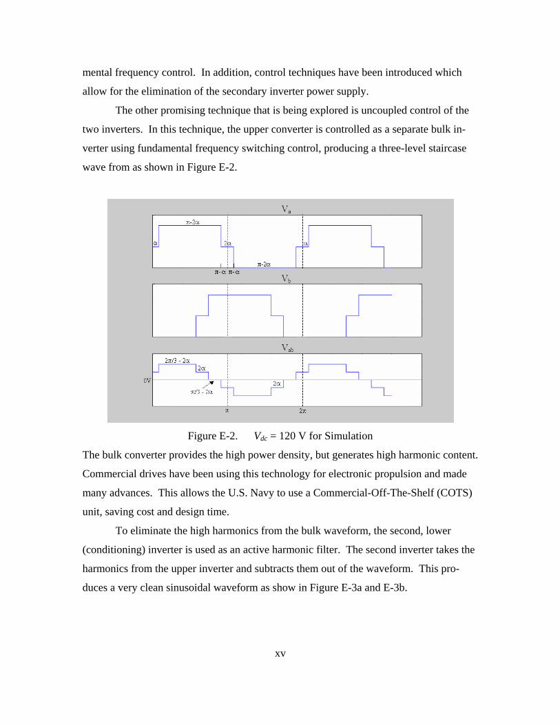
The other promising technique that is being explored is uncoupled control of the
two inverters. In this technique, the upper converter is controlled as a separate bulk in-
verter using fundamental frequency switching control, producing a three-level staircase
wave from as shown in Figure E-2.
Figure E-2. Vdc = 120 V for Simulation
The bulk converter provides the high power density, but generates high harmonic content.
Commercial drives have been using this technology for electronic propulsion and made
many advances. This allows the U.S. Navy to use a Commercial-Off-The-Shelf (COTS)
unit, saving cost and design time.
To eliminate the high harmonics from the bulk waveform, the second, lower
(conditioning) inverter is used as an active harmonic filter. The second inverter takes the
harmonics from the upper inverter and subtracts them out of the waveform. This pro-
duces a very clean sinusoidal waveform as show in Figure E-3a and E-3b.
xv
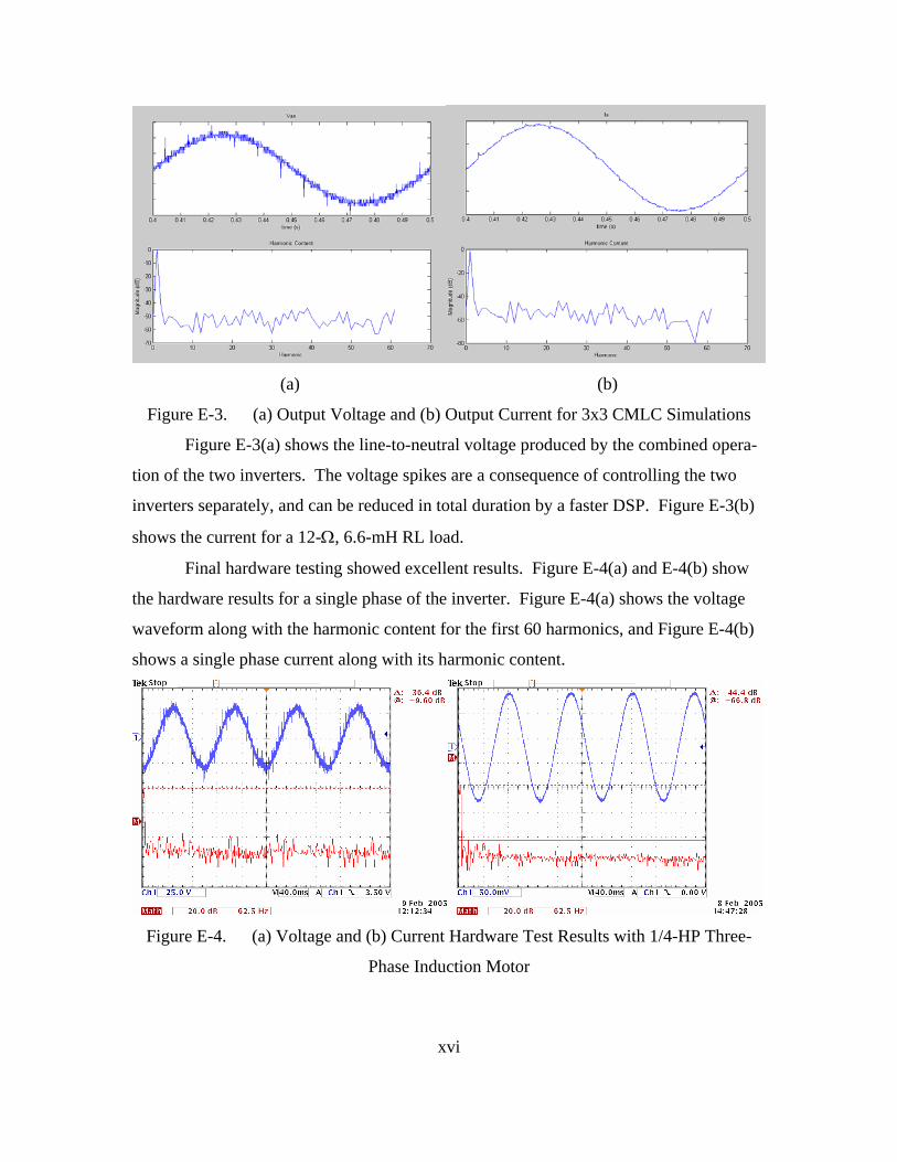
(a) (b)
Figure E-3. (a) Output Voltage and (b) Output Current for 3x3 CMLC Simulations
Figure E-3(a) shows the line-to-neutral voltage produced by the combined opera-
tion of the two inverters. The voltage spikes are a consequence of controlling the two
inverters separately, and can be reduced in total duration by a faster DSP. Figure E-3(b)
shows the current for a 12-Ω, 6.6-mH RL load.
Final hardware testing showed excellent results. Figure E-4(a) and E-4(b) show
the hardware results for a single phase of the inverter. Figure E-4(a) shows the voltage
waveform along with the harmonic content for the first 60 harmonics, and Figure E-4(b)
shows a single phase current along with its harmonic content.
Figure E-4. (a) Voltage and (b) Current Hardware Test Results with 1/4-HP Three-
Phase Induction Motor
xvi

xvii
The results in Figure E-4 show exceptional performance. The highest harmonic
content of the current waveform is over 44 dB less than the fundamental, resulting in a
high fidelity current output. The THD for the current was found to be 1.74%.

xviii
THIS PAGE INTENTIONALLY LEFT BLANK
1
I. INTRODUCTION
A. NAVAL POWER Before World War II, most naval vessels were electric drive because of the diffi-
culty in manufacturing high quality gears. However, as manufacturing processes im-
proved and shaft power requirements increased, mechanical drive systems became more
advantageous. Currently we are on the cusp of a switch back to electrical from mechani-
cal, but this time for the following reasons:
• Unlock propulsion power for other ship systems (e.g., pulse weapons)
• More efficient power utilization (matches power plant to load)
• Eliminate gearing with direct-drive motors.
The current switch to electric drive systems is being driven less by a lack of qual-
ity mechanical drives, and more by the increased electrical power needs of today’s de-
stroyers. Future U.S. Navy power applications include pulse weapon systems and Elec-
troMagnetic Aircraft Launch and Recovery Systems (EMALS and EARS). These loads
would easily overwhelm the current ship-service (or hotel) buses on destroyers [1]. Fur-
ther, incorporating unique dedicated generators for each application may cause the ship to
miss its weight and volume targets and become cost prohibitive [1]. Currently, up to
80% of a destroyer’s power generation is locked in the mechanical propulsions system.
By switching to all-electric propulsion, the ship’s propulsion power can also be used for
the high power electrical loads. It is important to note that the ship propulsion power is
related approximately to the cube of speed [2]. This translates into the ship only using
12% of its total propulsion power when cruising at half speed [2], freeing up the other
88% for high power application use.
Figure 1 depicts the increase in power generation capability in U.S. Navy De-
stroyers over time. Despite the 1000% growth in power generation since the end of
World War II, available power aboard destroyers is still insufficient to supply even a sin-
gle 30-MW advanced weapon system or launch.
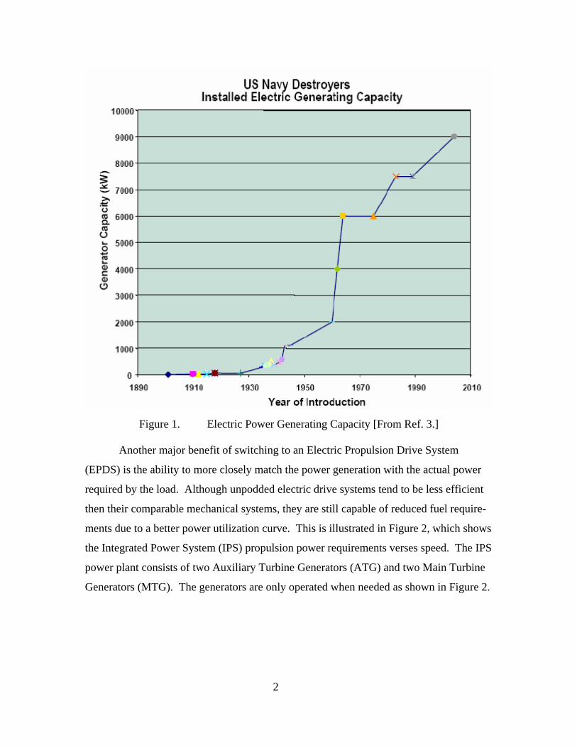
Figure 1. Electric Power Generating Capacity [From Ref. 3.]
Another major benefit of switching to an Electric Propulsion Drive System
(EPDS) is the ability to more closely match the power generation with the actual power
required by the load. Although unpodded electric drive systems tend to be less efficient
then their comparable mechanical systems, they are still capable of reduced fuel require-
ments due to a better power utilization curve. This is illustrated in Figure 2, which shows
the Integrated Power System (IPS) propulsion power requirements verses speed. The IPS
power plant consists of two Auxiliary Turbine Generators (ATG) and two Main Turbine
Generators (MTG). The generators are only operated when needed as shown in Figure 2.
2

Figure 2. Propulsion Power Requirements vs. Speed [From Ref. 3.]
A U.S. destroyer has a typical cruising speed of 12 to 14 knots. As shown in Fig-
ure 2, this requires only the two ATGs. The system was designed to operate the two
ATGs at their most efficient point at the most common cruising speed. Mechanical drive
systems operate at inefficient turbine points at common cruising speeds and only operate
efficiently at full power. Further, the two MTGs are free for high power weapon or
launch systems.
A final benefit of switching to electric drive systems is the ability to go to a direct
drive motor. This eliminates all gearing and reduces shafting (or eliminates shafting if
podded), which increases overall reliability and decreases the required amount of mainte-
nance. With the growth of EPDS in the commercial maritime industry, the technology
has matured to a point where the U.S. Navy can start to consider it as a viable alternative
to current mechanical drives systems.
B. PROPULSION REQUIREMENTS Both the U.S. Navy and the commercial maritime industry look at the same fac-
tors when comparing drive systems. These factors are stealth, space, cost, and reliability
and maintenance. The commercial industry was able to use electric drive systems that
3

outperform their mechanical counterparts in all four areas by using podded propulsion
[4]. A podded propulsion system mounts the motor in a compact package known as the
pod, which is attached outside the hull, and eliminates the need for expensive mechanical
drive components. Figure 3 shows an example of a commercially available pod.
Figure 3. ALSTOM 20MW Azimuth Pod (MermaidTM) [From Ref. 4.] The U.S. Navy has chosen not to pursue podded propulsion on the DD(X), but it
is still being evaluated as a possibility for future naval vessels [5].
1. Stealth Naval ships need to be stealthy in the water, especially in battle. Unlike the
commercial maritime industry, the U.S. Navy is constrained by the overall platform sig-
nature performance of their drive systems. This includes both the acoustic and electro-
magnetic signatures of the entire shipboard power generation and conversion systems.
These vital requirements in the ship’s signature are becoming more stringent. This is il-
lustrated by the recent reduction of five for a ship’s global electromagnetic limit [1].
Stealth to the commercial industry deals with audible drive system noise and
overall passenger comfort. By mounting the complete drive systems outside the hull, the
commercial maritime industry was able to greatly reduce overall system noise and in-
crease passenger comfort [4]. Unfortunately, the commercial industry is not concerned
with underwater acoustic and transmitted electromagnetic signatures. Therefore the pod-
ded system and the majority of current commercial propulsion system designs lack mili-
tary-grade filtering, making them unsuitable for military use.
2. Space The podded propulsion system has solved the commercial industry’s need to save
space for passengers and cargo because of its compact outer-hull design [4]. However,
the U.S. Navy has chosen not to pursue podded propulsion systems in the current DD(X)
4

5
design [5]. Initially there were two proposed DD(X) designs, one with podded propul-
sion and one with an internal power system [5]. The unpodded propulsion system design
was chosen because it could easily be converted back to a mechanical system and due to
concern of the overall noise of commercial podded systems [5].
Since the U.S. Navy is currently not pursuing podded propulsion, an alternative
needs to be developed that maximizes the power density and specific power of the system
to reduce overall size. In addition, the stealth requirement inadvertently makes the drive
converter larger, due to a need for a high fidelity current waveform. The need for addi-
tional passive or active filtering components can become voluminous.
3. Cost Probably the most crucial area is cost. Since the entire commercial maritime in-
dustry is moving towards all-electric propulsion, the cost for these systems has become
very affordable. In addition, a commercial podded propulsion system consumes 30% less
fuel then a non-podded equivalent [4]. This is the result of a more hydrodynamic hull
design optimized by the use of pods [4].
Mechanical drive systems may become prohibitively expensive without any
commercial industry backing. With the entire commercial industry moving towards elec-
tric propulsion, it is beneficial that the military follow suit.
The small quantity of military specialty drives may not be a factor for the future
maritime market. Therefore, for the military to keep expenses down, the U.S. Navy must
learn to incorporate commercial items with little or no design modifications. The focus
of this thesis is incorporating a commercially available bulk power converter with a
smaller, dedicated conditioning converter to create a stealthy system that saves space and
cost.
4. Reliability and Maintenance. The commercial industry has been able to create very reliable and low mainte-
nance systems using podded propulsion. By using direct-drive, gearing and shafting are
eliminated from the drive systems, reducing maintenance to only the electric components
and the motor itself. These components tend to be very reliable and require little mainte-
nance.

Even without using podded propulsion, the U.S. Navy can still take advantage of
the reliability of electric systems and the elimination of gearing, by use of a direct-drive
system. However, U.S. Naval systems also have the additional requirement of being bat-
tle hardened. Propulsion systems in a naval vessel are going to be subjected to stresses
that would not be seen in a commercial ship. In addition to normal operation of a naval
ship, naval systems have to handle the extreme conditions that a ship undergoes during
battle, including long operational commitments and extreme degrees of shock and vibra-
tion. Since this area has more to do with the physical construction and physical isolation
of the system, it is not covered in this thesis.
C. PROPULSION SYSTEMS A propulsion system consists of four parts:
• AC-source: typically a three-phase turbine generator
• Rectification: diode or active front end
• DC link: may be as simple as an LC-filter
• Inversion: various topologies described below.
Figure 4 shows a block diagram of a complete EPDS.
Figure 4. Propulsion System Block Diagram
This thesis concentrates on the inversion portion of the drive, and utilizes a volt-
age source inverter. However, it is important to keep in mind the other drive compo-
nents, since cost can be lowered through modular design. A modular design allows for
the use of the same structures or building blocks in different parts of the system. For in-
stance, it is common to use the exact same power electronic modules for the “Rectifica-
tion” and the “Inversion”. This philosophy can reduce inventory and maintenance train-
ing as well as overall cost.
6

7
There are various inverter topologies available that are well suited for modular
designs. These include the H-bridge, two-level, Neutral Point Clamped (NPC), multi-
level, and Cascaded Multi-Level Converter (CMLC). These topologies are discussed in
detail in Chapter II. The focus of this thesis is using a CMLC that consists of a Commer-
cial-Off-The-Shelf (COTS) bulk inverter and a navy specific conditioning inverter. In
this form, the CMLC can be controlled in an uncoupled manner, e.g., the bulk inverter
operates independently of the conditioning inverter. The bulk inverter utilizes a funda-
mental-frequency switching control algorithm. The conditioning inverter can utilize any
number of control algorithms. Two possible conditioning inverter control algorithms are
discussed in detail in this thesis.
D. THESIS GOAL The goal of this thesis is to develop and test an uncoupled controlled 3x3 CMLC.
This involved developing a control algorithm for the conditioning inverter and an algo-
rithm to extract the reference sine wave information from the bulk inverter. Distortion
and transition spikes are used to compare algorithms. Further, dynamic testing was done
to determine the tracking accuracy of the output to the reference sine wave.
E. THESIS OVERVIEW The next chapter gives a review of common inverter topologies, and introduces
the 3x3 CMLC previously built at Naval Postgraduate School (NPS). Chapter III intro-
duces uncoupled control for a CMLC and discusses a simple technique for developing the
reference sine wave of the bulk inverter. Chapter IV covers two separate algorithms de-
veloped to control the conditioning inverter, one utilizing a modified SVM algorithm and
the other utilizing a unique PWM technique that eliminates the need for reference triplen
harmonics. Chapter V implements these algorithms in Simulink, and then downloads
them into the DS1103 PPC board to do hardware tests. Chapter VI presents the results of
the testing, and Chapter VII reports the conclusions.

8
THIS PAGE INTENTIONALLY LEFT BLANK
II. INVERTERS
A. OVERVIEW This chapter covers the various inverter topologies available. Control strategies
are mentioned, but are covered in more detail in Chapter IV. Finally, the chapter details
the previous work done with the 3x3 CMLC currently residing at NPS.
B. INVERTER TOPOLOGIES There are several types of commercially available voltage source inverters. Basic
single-phase topologies include the half-bridge and H-Bridge. Single-phase topologies
combine to form multiphase inverters for high power. Multi-phase topologies include the
two-level, NPC, multi-level and CMLC. An important direct ac-ac topology known as
the cycloconverter is worth mentioning because of its successful application in the Coast
Guard Icebreaker Healy [16]. Because of their robustness, they are pegged for a future
NPS thesis topic in conjunction with a non-standard high frequency generator. However,
cycloconverters are not inverters and not the topic of this thesis.
The half-bridge inverter is generally not used for high voltage applications since
its structure underutilizes the source dc bus. However, the H-bridge, which consists of
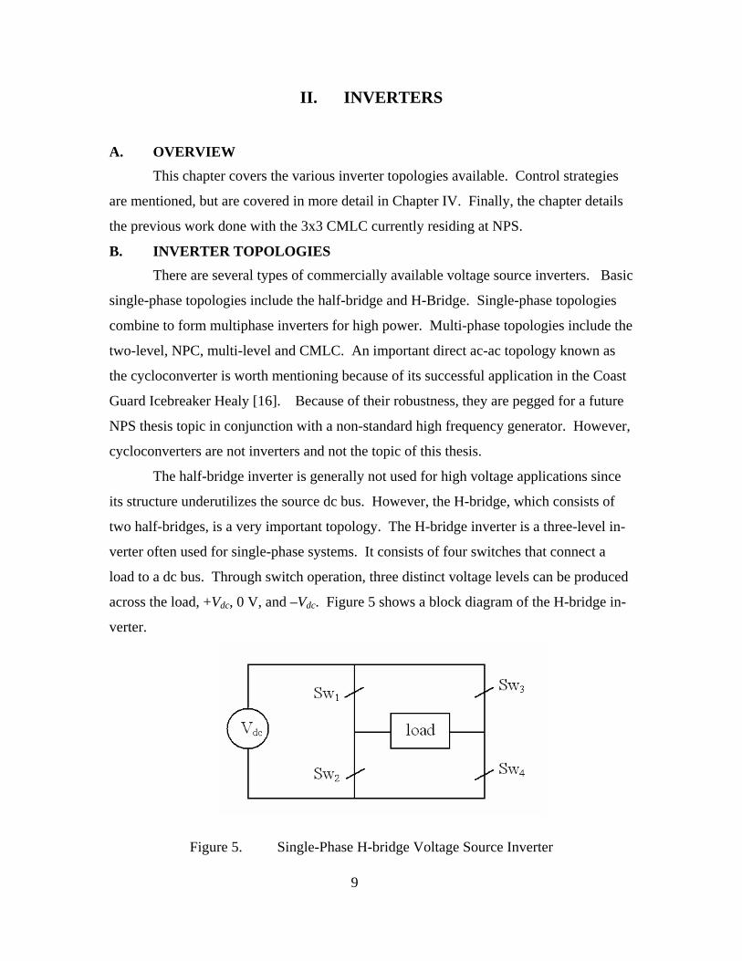
two half-bridges, is a very important topology. The H-bridge inverter is a three-level in-
verter often used for single-phase systems. It consists of four switches that connect a
load to a dc bus. Through switch operation, three distinct voltage levels can be produced
across the load, +Vdc, 0 V, and –Vdc. Figure 5 shows a block diagram of the H-bridge in-
verter.
Figure 5. Single-Phase H-bridge Voltage Source Inverter
9
This topology can be extended to multi-phase loads with isolated individual windings.
Many three-phase loads do not have completely accessible windings and require other
poly-phase topologies for operation.
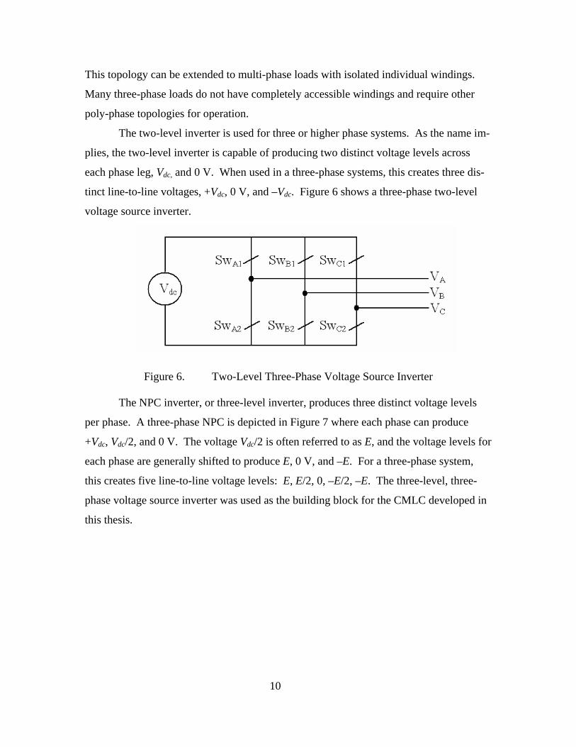
The two-level inverter is used for three or higher phase systems. As the name im-
plies, the two-level inverter is capable of producing two distinct voltage levels across
each phase leg, Vdc, and 0 V. When used in a three-phase systems, this creates three dis-
tinct line-to-line voltages, +Vdc, 0 V, and –Vdc. Figure 6 shows a three-phase two-level
voltage source inverter.
Figure 6. Two-Level Three-Phase Voltage Source Inverter The NPC inverter, or three-level inverter, produces three distinct voltage levels
per phase. A three-phase NPC is depicted in Figure 7 where each phase can produce
+Vdc, Vdc/2, and 0 V. The voltage Vdc/2 is often referred to as E, and the voltage levels for
each phase are generally shifted to produce E, 0 V, and –E. For a three-phase system,
this creates five line-to-line voltage levels: E, E/2, 0, –E/2, –E. The three-level, three-
phase voltage source inverter was used as the building block for the CMLC developed in
this thesis.
10

Figure 7. Three-Level Three-Phase NPC Voltage Source Inverter [From Ref. 7.] The multi-level inverter topology is an extension of the three-level. By adding
more switches, diodes, and capacitors, the DC bus voltage can be divided into more lev-
els. As level count increases, so does the fidelity of the output waveform regardless of
controller algorithm. This is analogous to the number of bits in a D/A converter. A
higher bit converter is capable of producing a better analog output. As the levels in-
crease, so does the complexity of the hardware and switch mapping control. For an n-
level multi-level inverter, there are n distinct voltage levels produced per phase, and (2n–
1) line-to-line voltage levels. The DD(X) design uses a five-level inverter for its propul-
sion system [3].
The CMLC is a further extension to the multi-level inverter topology. A CMLC
consists of two multi-level inverters cascaded through the load [6] as shown in Figure 8.
11

Figure 8. 3x3 Cascaded Multi-Level Converter [From Ref. 7.]
The upper inverter acts as a bulk inverter and supplies the majority of the power
to the load, while the lower inverter acts as a conditioning inverter, vastly improving the
power quality to the load [2]. CMLCs are classified by multiplying the number of levels
of the upper inverter and the number of levels of the lower inverter. For example, a
CMLC with an NPC upper inverter and an NPC lower inverter would be called a 3x3
CMLC.
A CMLC can be treated as a single multi-level inverter of equivalent number of
levels. This substantially lowers the switch count when compared with a multi-level in-
12

verter of equal equivalent level. However, the actual number of voltage levels produced
by a CMLC varies, based on the ratio of the voltage across the upper inverter (Vdc) to the
voltage across the lower inverter (Vdcx). A useful technique for viewing the different
voltage levels produced by a CMLC is to look at the output in the q-d reference frame [2,
8] for varying ratios of Vdc to Vdcx. The q-d refers to quadrature-direct and is a transform
for simplifying conventional three phase systems. The q-d transform takes the three-
phase abc components and transforms them into an orthogonal two dimensional reference
frame. In the case of unbalanced loads, a zero sequence must also be considered; how-
ever this thesis focuses solely on balanced loads. The q-d reference frame is discussed in
more depth in Chapter III.
The first step is to convert the output voltages of the CMLC into line-to-neutral
voltages using [2]
2 1 1
1 1 2 13
1 1 2
as a ax
bs b bx
cs c cx
v vvv v
−− −⎡ ⎤ ⎡ ⎤⎡ ⎤⎢ ⎥ ⎢ ⎥⎢ ⎥= − − −⎢ ⎥ ⎢ ⎥⎢ ⎥⎢ ⎥ ⎢ ⎥⎢ ⎥− − −⎣ ⎦⎣ ⎦ ⎣ ⎦
.v
v vv
(2.1)
The next step is to convert the line-to-neutral voltages into the q-d stationary reference
frame using [2]
2 1 13 2 2qs as bs csv v v v⎛= − −⎜
⎝ ⎠⎞⎟ (2.2)
and
(1 .3ds cs bsv v v= − ) (2.3)
By stepping through all possible switching states for the CMLC, a pattern is uncovered,
which represents the switching states for the converter in the q-d reference frame. Figure
9 shows the available switching states for four different input voltage ratios in the q-d
reference frame.
13

Figure 9. Vector Plots for Different Voltage Ratios [After Ref. 2.]
The goal is to find the ratio that creates maximal distention. In other words, the
ratio that creates the greatest number of equally spaced switching states. As shown
above, Vdc/3 creates the pattern of maximal distention [2]. The point of maximal disten-
tion creates an equivalent switching pattern to a multi-level inverter with a level equal to
3 3 9m x n x= = (2.4)
where m is the level of the upper bulk inverter and n is the level of the lower conditioning
inverter. A CMLC consisting of two NPC inverters was used throughout this thesis.
C. CONTROL ALGORITHMS FOR INVERTERS
There are several control techniques for multi-level inverters, including: funda-
mental-frequency switching control, space vector modulation (SVM), sine-triangle pulse
width modulation (SPWM), sub-harmonic PWM methods [9], and switching frequency 14
15
optimal PWM [9]. Fundamental-frequency switching control, SVM, and SPWM are dis-
cussed in detail in this thesis along with a new hybrid algorithm. Information about the
sub-harmonic PWM technique can be found in Reference 10, and information about
switching frequency optimal PWM can be found in Reference 11.
These control strategies can also be implemented with a CMLC when considered
as a single multi-level inverter with equivalent number of levels. However, the primary
benefit of the CMLC is the ability to control each inverter separately. Controlling the
CMLC as a single equivalent multi-level inverter is referred to as joint control, and con-
trolling the CMLC as two separate inverters is referred to as uncoupled control.
Uncoupled control allows the use of a Commercial-Off-The-Shelf (COTS) bulk
inverter utilizing a fundamental-frequency switching control algorithm [6]. Due to the
high power density and high specific power of inverters utilizing fundamental-frequency
switching control algorithms, the overall footprint of the system is reduced. Further, the
use of an uncoupled unmodified COTS inverter reduces overall cost when compared with
an equivalent high-power, high-fidelity, Navy-specific solution.
The conditioning inverter is a dedicated inverter specifically built for the U.S.
Navy using an advanced control algorithm; however, due to the fact that it operates at 1/3
the bus voltage, it is significantly smaller and less expensive to build, and dissipates less
power at high frequency switching than its bulk counterpart. This thesis demonstrates
that the pair of inverters is capable of dramatically reducing the Total Harmonic Distor-
tion (THD) of the output waveform (compared to a single COTS unit), which enables
stealthy ship propulsion. A final benefit of uncoupled control is system redundancy. As
stated earlier, the ship’s propulsion power is related to the cube of the ship’s speed. If the
bulk converter were to be damaged, the conditioning converter could be used to propel
the ship, albeit at a reduced speed.
D. NPS-BUILT 3X3 NEUTRAL-POINT CLAMPED CASCADED MULTI-LEVEL CONVERTER
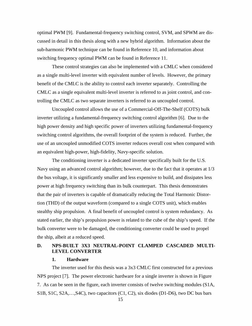
1. Hardware
The inverter used for this thesis was a 3x3 CMLC first constructed for a previous
NPS project [7]. The power electronic hardware for a single inverter is shown in Figure
7. As can be seen in the figure, each inverter consists of twelve switching modules (S1A,
S1B, S1C, S2A,…,S4C), two capacitors (C1, C2), six diodes (D1-D6), two DC bus bars
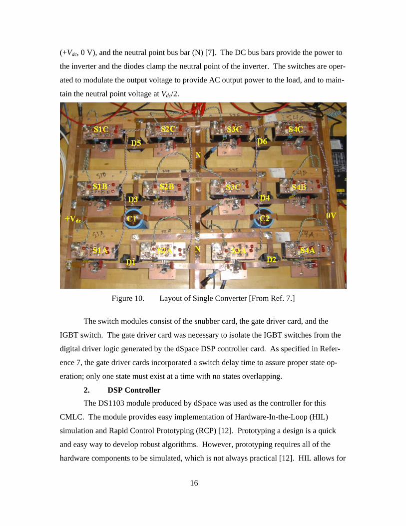
(+Vdc, 0 V), and the neutral point bus bar (N) [7]. The DC bus bars provide the power to
the inverter and the diodes clamp the neutral point of the inverter. The switches are oper-
ated to modulate the output voltage to provide AC output power to the load, and to main-
tain the neutral point voltage at Vdc/2.
Figure 10. Layout of Single Converter [From Ref. 7.]
The switch modules consist of the snubber card, the gate driver card, and the
IGBT switch. The gate driver card was necessary to isolate the IGBT switches from the
digital driver logic generated by the dSpace DSP controller card. As specified in Refer-
ence 7, the gate driver cards incorporated a switch delay time to assure proper state op-
eration; only one state must exist at a time with no states overlapping.
2. DSP Controller
The DS1103 module produced by dSpace was used as the controller for this
CMLC. The module provides easy implementation of Hardware-In-the-Loop (HIL)
simulation and Rapid Control Prototyping (RCP) [12]. Prototyping a design is a quick
and easy way to develop robust algorithms. However, prototyping requires all of the
hardware components to be simulated, which is not always practical [12]. HIL allows for
16

actual hardware to be connected to the simulation through the DSP interface. The dSpace
interface consists of the DSP card, DSP I/O board, and the DSP software interface.
The DS1103 PPC controller board is a single-board system that inserts into a
standard Peripheral Component Interconnect (PCI) card slot. The board utilizes a slave
Texas Instruments TMS320F240 DSP running at a 20-MHz clock rate. The board con-
tains 4 16-bit ADCs with a 4-µs conversion time, and 4 12-bit ADCs with 0.8-µs conver-
sion time, along with a 32-bit digital I/O bus. Figure 11 shows the controller board.
Figure 11. DS1103 PPC Controller Board [From Ref. 13.]
The dSpace CP1103 I/O Board shown in Figure 12, provides the numerous input
and output ports. A 50-pin digital I/O connector was used to connect the CP1103 to the
3x3 CMLC. Four coaxial cables were used to feed the analog inputs into the ADCs.
17

Figure 12. CP1103 I/O Board [From Ref. 14.] The DSP software interface consisted of two components. The first component is
a Simulink interface with a real-time compiler. This interface allows a software simula-
tion model to be quickly converted to code and downloaded into the DSP card. The sec-
ond component is the Control Desk Interface, which allows the user to compile the Simu-
link code and load it into the card. The Control Desk has the added benefits of allowing
the user to view the signals in the card and change parameters in the simulation during
operation. More information on the DSP system can be found in References 12, 13, and
14.
3. Control Algorithm
The control algorithm chosen to run the hardware in Reference 7 was a simple
SPWM algorithm utilizing joint control. SPWM was chosen for the first control algo-
rithm due to its overall simplicity and excellent performance. The algorithm was based
on generating a reference sine wave for each phase, and comparing that reference wave-
form with stacked triangle waveforms operating at the desired switching frequency. The
number of stacked triangle waveforms corresponds to the number of levels of the inverter
minus one. For a 3x3 CMLC, the total number of equivalent levels is nine, which corre-
sponds to eight stacked triangle waveforms as shown in Figure 13.
18

Figure 13. Sine Triangle Waveform [From Ref. 7.] Each triangle waveform corresponds to a different switch state. When the refer-
ence sine wave is above a given triangle, then the algorithm outputs that given state. For
example, switching state “0” exists when the reference sine wave is less than the bottom
triangle wave, and state “1” exists when the reference wave is greater than the bottom
triangle wave. The switching states are then decoded to determine the position (“on” or
“off”) of each individual switch in the inverter. Table 1 gives the decoded signals for
each switch for a single phase of the 3x3 inverter where S1, S2, S3, and S4 correspond to
the upper inverter, and S1x, S2x, S3x, and S4x correspond to the lower inverter.
19
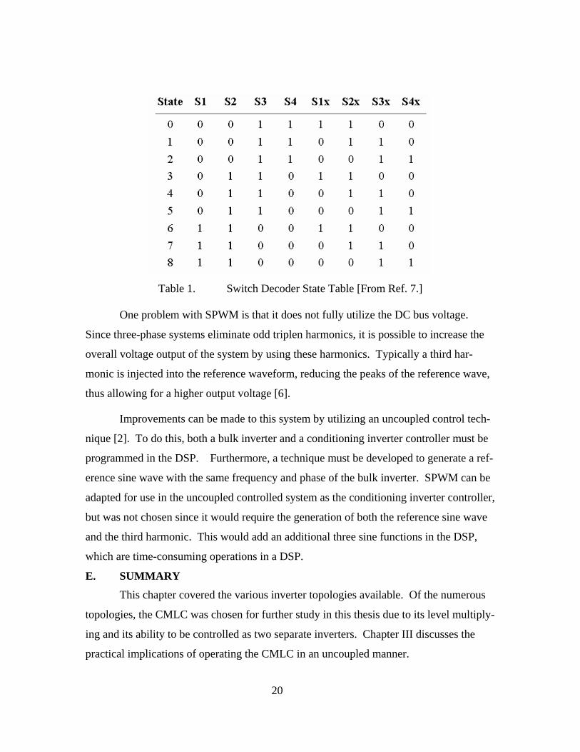
Table 1. Switch Decoder State Table [From Ref. 7.]
One problem with SPWM is that it does not fully utilize the DC bus voltage.
Since three-phase systems eliminate odd triplen harmonics, it is possible to increase the
overall voltage output of the system by using these harmonics. Typically a third har-
monic is injected into the reference waveform, reducing the peaks of the reference wave,
thus allowing for a higher output voltage [6].
Improvements can be made to this system by utilizing an uncoupled control tech-
nique [2]. To do this, both a bulk inverter and a conditioning inverter controller must be
programmed in the DSP. Furthermore, a technique must be developed to generate a ref-
erence sine wave with the same frequency and phase of the bulk inverter. SPWM can be
adapted for use in the uncoupled controlled system as the conditioning inverter controller,
but was not chosen since it would require the generation of both the reference sine wave
and the third harmonic. This would add an additional three sine functions in the DSP,
which are time-consuming operations in a DSP.
E. SUMMARY
This chapter covered the various inverter topologies available. Of the numerous
topologies, the CMLC was chosen for further study in this thesis due to its level multiply-
ing and its ability to be controlled as two separate inverters. Chapter III discusses the
practical implications of operating the CMLC in an uncoupled manner.
20

21
III. UNCOUPLED CONTROL
A. OVERVIEW
This chapter details an uncoupled method of controlling a CMLC. Thus, it pre-
sents the ramifications of an autonomous bulk inverter as a part of the cascade. Some
limitations of the chosen technique are also discussed. Finally, digital spiking caused by
the discrete nature of DSPs is mentioned, but reduction techniques are left to Chapter IV.
B. UNCOUPLED CONTROL Although a CMLC can be controlled as a single equivalent multi-level inverter,
this is undesirable for U.S. Navy purposes. As presented in Chapter II, component count
and complexity decrease when a single multi-level is replaced with an equivalent cas-
caded version. The separability of high power and high fidelity functions allows the use
of a COTS bulk converter with a low-power, low-cost, Navy-specific inverter for active
filtering. Figure 14 shows the configuration of the CMLC used in this thesis.
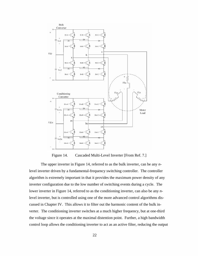
Figure 14. Cascaded Multi-Level Inverter [From Ref. 7.]
The upper inverter in Figure 14, referred to as the bulk inverter, can be any n-
level inverter driven by a fundamental-frequency switching controller. The controller
algorithm is extremely important in that it provides the maximum power density of any
inverter configuration due to the low number of switching events during a cycle. The
lower inverter in Figure 14, referred to as the conditioning inverter, can also be any n-
level inverter, but is controlled using one of the more advanced control algorithms dis-
cussed in Chapter IV. This allows it to filter out the harmonic content of the bulk in-
verter. The conditioning inverter switches at a much higher frequency, but at one-third
the voltage since it operates at the maximal distention point. Further, a high bandwidth
control loop allows the conditioning inverter to act as an active filter, reducing the output
22

waveform to a nearly pure sinusoid at the desired frequency. The active filtering with the
lower bus voltage requires a power rating of approximately one-tenth that of the bulk
converter.
In order to actively filter the harmonic content of the bulk inverter waveform, an
error signal representing only harmonic information must be uncovered. This is done by
first generating a reference sine wave locked to the frequency of the bulk converter as
shown in Figure 15.
Figure 15. Bulk Converter Output With Reference Sine Wave
By properly adjusting the magnitude and phase of the reference fundamental, an
error signal containing only harmonic information can be extracted by simple subtraction
[2].
, ,
,
, , .
ag h ag ag f
bg h bg bg f
cg h cg cg f
v v v
v v v
v v v,
= −
= −
= −
(3.1)
The harmonic-only signals (Figure 16) are then used as the command voltages for the
conditioning inverter.
23
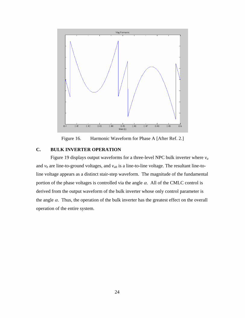
Figure 16. Harmonic Waveform for Phase A [After Ref. 2.]
C. BULK INVERTER OPERATION
Figure 19 displays output waveforms for a three-level NPC bulk inverter where va
and vb are line-to-ground voltages, and vab is a line-to-line voltage. The resultant line-to-
line voltage appears as a distinct stair-step waveform. The magnitude of the fundamental
portion of the phase voltages is controlled via the angle α. All of the CMLC control is
derived from the output waveform of the bulk inverter whose only control parameter is
the angle α. Thus, the operation of the bulk inverter has the greatest effect on the overall
operation of the entire system.
24

Figure 17. Bulk Inverter Output Waveform [After Ref. 2.]
The relationship between the peak value of the fundamental vfund, the dc bus volt-
age Vdc, and the control angle α, appears in the following equation [2]
2 cos( )dcfund
Vv απ
= . (3.2)
The valid control angles are 0° < α < 90°. As α is adjusted, the commanded magnitude
of the output fundamental voltage changes and the CMLC control operators are affected.
This is apparent due to a change in the available switching states and a necessary adjust-
ment to the reference sine wave.
The output angle α has an extreme impact on the available output voltage vectors
for a CMLC using uncoupled control. By transforming the system into the q-d reference
frame as was done in Chapter II, and plotting the available output states of the system for
several different angles, the affect of α can be seen. Figures 18, 19, and 20 show the out-
put states for a 3x3 CMLC with α = 0º, α = 15º, and α = 45º, respectively. The blue dots
represent the standard switching states available for a jointly controlled 3x3 CMLC. The
black circles represent the switching states available for a 3x3 CMLC using uncoupled
control with the bulk converter operating with the given control angle α. 25
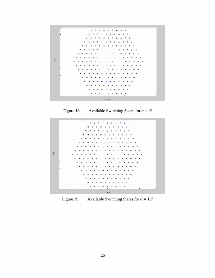
Figure 18. Available Switching States for α = 0º
Figure 19. Available Switching States for α = 15°
26

Figure 20. Available Switching States for α = 45°
As seen from these three figures, the available output switching states change
drastically as the control angle varies. An α of 15°, which was used in Reference 2, was
used throughout this thesis. With this α, the system cannot adequately represent lower
voltages due to the lack of switching states. There are two fixes to this. The first is to
use the conditioning inverter alone, and the second is to use a controllable DC front end.
Operating the conditioning inverter alone reduces the level of the system to three, thus
increasing THD. By utilizing a controllable DC front end any voltage can be emulated
while employing all the available voltage levels of the inverter, thus producing the high-
est quality output waveform.
The control angle α also influences the generation of the reference sine wave.
There are several ways to generate the reference sine wave. Two methods are evaluated
below. One method is independent of α, but involves filtering and complex computa-
tions. It continually updates the frequency, but always lags by the filter delay [6]. The
other method uses α and an integrator as a timer. It updates the frequency at discrete in-
tervals where the maximum update rate is 12 times per period of the output sine wave.
27

Figure 21. Block Diagram for q-d Reference Sine Wave Generation [After Ref. 6.] The first method finds the line-to-neutral voltages (vas, vbs, and vcs) utilizing the
transformation introduced in Chapter II, Equation (2.1). These voltages are then filtered
to create sine waves whose steady-state frequency matches the bulk converter reference
sine wave. Once the fundamental components are found, the cosine and sine of the elec-
trical angle can be uncovered using the following equations [6].
( )2 2 2
3cos2
ase
as bs cs
vv v v
θ =+ +
(3.3)
and
( )2 2 2
1sin2
cs bse
as bs cs
v vv v v
θ −=
+ + (3.4)
With the cosine and sine of the electrical angle known, the bulk inverter output
voltages can be transformed into the synchronous q-d reference frame, and then filtered
to create the desired output voltages, and . The original transformed voltages
and are then subtracted from the filtered and voltages. This results in the
commanded and voltages, which are then transformed back to the stationary abc
reference frame. These transformed voltages are then used as the commanded voltages
for the conditioning inverter. More detailed information can be found in Reference 6.
eqov e
dov
eqov e
dov eqov e
dov
*eqsxv *e
dsxv
The second method does not require any transformations or complex equations,
but is dependent on the control angle, α. For this implementation, the frequency is found
by using an integrator to measure the time of a bulk inverter output state (refer to Figure
17). With the time t found for a single output state, the total period of the bulk inverter
waveform can be found. First the proportion P of the total period of the output state is
found by
28

2LPπ
= , (3.5)
where L is the length in radians of output state being timed. The lengths of the different
output states are shown in Figure 17, and are dependent on α. From this, the period is
found by
tTP
= , (3.6)
which reduces to
2T tLπ
= . (3.7)
Finally, the fundamental frequency is easily extracted,
12fundLf
T tπ= = , (3.8)
and, the angular frequency is
2fund fundLft
ω π= = . (3.9)
Multiplying the angular frequency with a timer that is reset with the rising edge of
each phase of the bulk inverter output and delayed by the control angle α, creates the ref-
erence sine wave in phase with the bulk inverter. The actual implementation is discussed
in the Chapter IV. This technique was used to generate the reference sine wave through-
out this thesis.
D. DIGITAL SPIKE ELIMINATION One consequence of uncoupled control is the creation of digital spikes [6]. This
anomaly occurs when the bulk inverter switches output states while the conditioning in-
verter is in the middle of a PWM cycle. Figure 22 shows a simulation of the 3x3 CMLC
containing associated spiking.
29
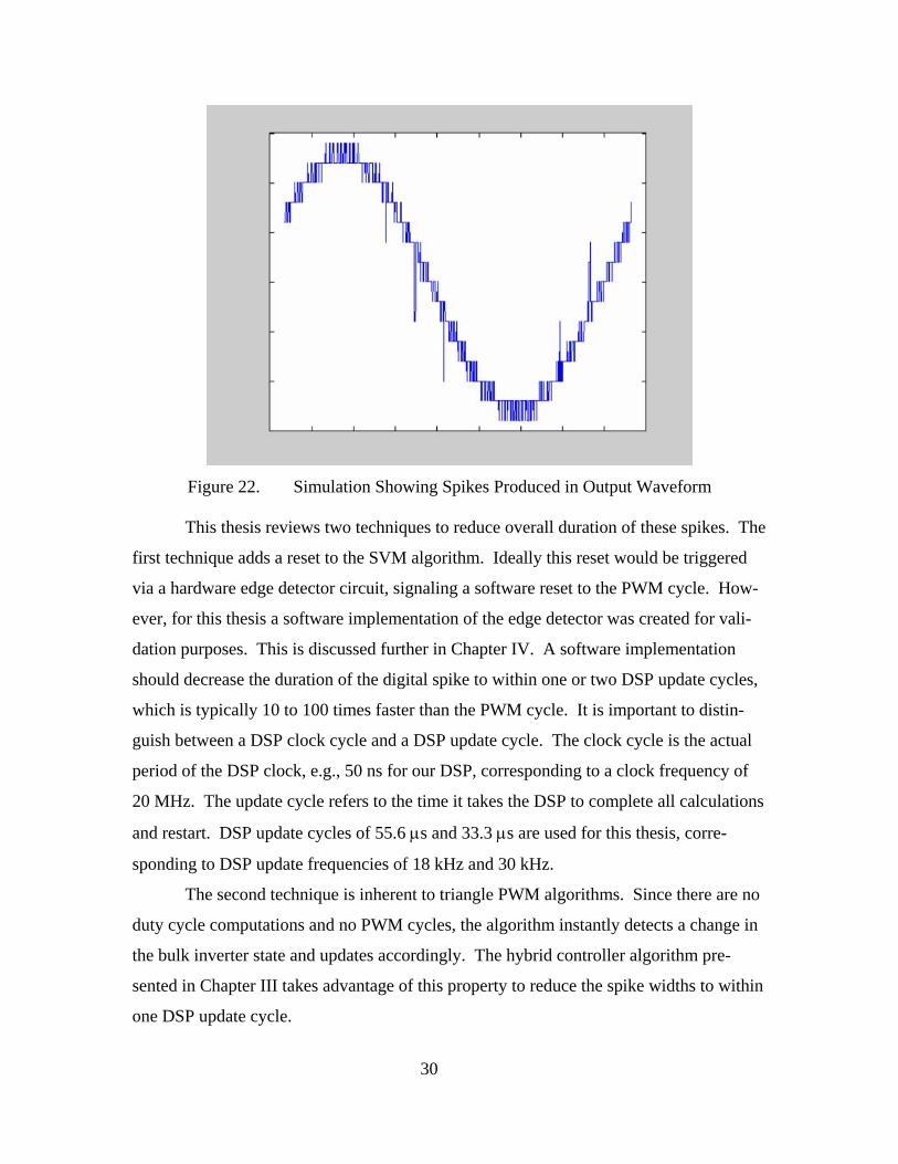
Figure 22. Simulation Showing Spikes Produced in Output Waveform
This thesis reviews two techniques to reduce overall duration of these spikes. The
first technique adds a reset to the SVM algorithm. Ideally this reset would be triggered
via a hardware edge detector circuit, signaling a software reset to the PWM cycle. How-
ever, for this thesis a software implementation of the edge detector was created for vali-
dation purposes. This is discussed further in Chapter IV. A software implementation
should decrease the duration of the digital spike to within one or two DSP update cycles,
which is typically 10 to 100 times faster than the PWM cycle. It is important to distin-
guish between a DSP clock cycle and a DSP update cycle. The clock cycle is the actual
period of the DSP clock, e.g., 50 ns for our DSP, corresponding to a clock frequency of
20 MHz. The update cycle refers to the time it takes the DSP to complete all calculations
and restart. DSP update cycles of 55.6 µs and 33.3 µs are used for this thesis, corre-
sponding to DSP update frequencies of 18 kHz and 30 kHz.
The second technique is inherent to triangle PWM algorithms. Since there are no
duty cycle computations and no PWM cycles, the algorithm instantly detects a change in
the bulk inverter state and updates accordingly. The hybrid controller algorithm pre-
sented in Chapter III takes advantage of this property to reduce the spike widths to within
one DSP update cycle.
30
31
An alternate method to reduce the spikes not used in this thesis is discussed in de-
tail in Reference 6. This technique nearly eliminates the spikes and is independent of the
DSP. However, it requires the use of additional hardware and software resulting in a
more complex system.
E. SUMMARY When operating a CMLC as two separate inverters, the bulk inverter control an-
gle, α, has several effects on the system. This includes the available switching states of
the system, the magnitude of the output voltage, and the generation of the reference sine
wave. A control angle of 15° was chosen to maximize the output voltage and minimize
the harmonic content of the bulk inverter. To generate the reference sine wave from the
bulk inverter, a digital timing technique was chosen due to its simplicity. Finally, two
techniques were introduced to reduce the digital spiking of the system, and are tested in
Chapter V. With the system set up for uncoupled control, Chapter IV examines possible
control algorithms for the conditioning inverter.

32
THIS PAGE INTENTIONNALY LEFT BLANK

33
IV. SPACE VECTOR MODULATION
A. OVERVIEW
This chapter details SVM algorithms. Two algorithms utilizing two different
transforms are introduced. The first algorithm is based on the q-d reference frame and is
shown to be significantly more complex than the second algorithm, which is based on the
g-h reference frame. Additionally, a hybrid algorithm developed specifically for this the-
sis is presented. The attributes of the second SVM algorithm and the hybrid algorithm
are compared by actual HIL implementation via the CMLC and dSpace controller.
B. SPACE VECTOR MODULATION
SVM has become a common control technique that can be used for multi-level
and cascaded multi-level inverters. All SVM techniques follow the same basic pattern
[10, 17, 18]:
• Transform into q-d reference frame (or g-h frame)
• Detect the three nearest vectors
• Determine the vector duty cycles
• Transform into relevant switching states.
SVM employs a two dimensional transformation to represent the three-phases of high
power systems. The two transformations commonly used are the Park’s transform, and
the g-h transform introduced in Reference 17. The Park’s equations convert the abc time
varying phase components into the orthogonal q-d reference frame [8]. The g-h trans-
form uses a 60° non-orthogonal basis to transform abc into the g-h reference frame. The
g-h transform greatly simplifies the detection of the nearest vectors, and reduces duty cy-
cle calculations to simple addition and subtraction when using SVM. Restated, both
transforms are generally used to emulate a three-phase power system in a simpler form.
A three-phase voltage supply reduces to a circle in the q-d reference frame [2] and
an ellipse in the g-h reference frame. Figure 23 shows a three-phase sinusoidal reference
voltage transformed into the q-d reference frame and overlaid onto the space vector plot
for a nine-level inverter.
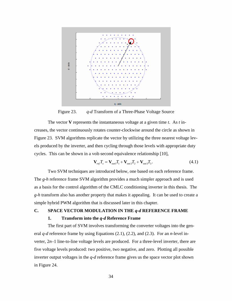
Figure 23. q-d Transform of a Three-Phase Voltage Source
The vector V represents the instantaneous voltage at a given time t. As t in-
creases, the vector continuously rotates counter-clockwise around the circle as shown in
Figure 23. SVM algorithms replicate the vector by utilizing the three nearest voltage lev-
els produced by the inverter, and then cycling through those levels with appropriate duty
cycles. This can be shown in a volt-second equivalence relationship [10],
1 1 2 2 3 3ref s out out outT T T T= + +V V V V . (4.1)
Two SVM techniques are introduced below, one based on each reference frame.
The g-h reference frame SVM algorithm provides a much simpler approach and is used
as a basis for the control algorithm of the CMLC conditioning inverter in this thesis. The
g-h transform also has another property that makes it appealing. It can be used to create a
simple hybrid PWM algorithm that is discussed later in this chapter.
C. SPACE VECTOR MODULATION IN THE q-d REFERENCE FRAME
1. Transform into the q-d Reference Frame
The first part of SVM involves transforming the converter voltages into the gen-
eral q-d reference frame by using Equations (2.1), (2.2), and (2.3). For an n-level in-
verter, 2n–1 line-to-line voltage levels are produced. For a three-level inverter, there are
five voltage levels produced: two positive, two negative, and zero. Plotting all possible
inverter output voltages in the q-d reference frame gives us the space vector plot shown
in Figure 24.
34
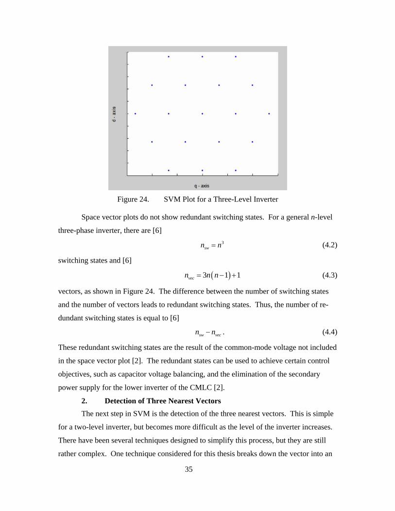
Figure 24. SVM Plot for a Three-Level Inverter
Space vector plots do not show redundant switching states. For a general n-level
three-phase inverter, there are [6]
3swn n= (4.2)
switching states and [6]
( )3 1vecn n n 1= − + (4.3)
vectors, as shown in Figure 24. The difference between the number of switching states
and the number of vectors leads to redundant switching states. Thus, the number of re-
dundant switching states is equal to [6]
sw ven n c− . (4.4)
These redundant switching states are the result of the common-mode voltage not included
in the space vector plot [2]. The redundant states can be used to achieve certain control
objectives, such as capacitor voltage balancing, and the elimination of the secondary
power supply for the lower inverter of the CMLC [2].
2. Detection of Three Nearest Vectors The next step in SVM is the detection of the three nearest vectors. This is simple
for a two-level inverter, but becomes more difficult as the level of the inverter increases.
There have been several techniques designed to simplify this process, but they are still
rather complex. One technique considered for this thesis breaks down the vector into an
35

offset component and a two-level component [10]. Figure 25 shows a three-level space
vector plot, with a commanded reference voltage, VRV, which breaks down into an offset
reference voltage, VRV(OFST), and a two-level component, VRV(twl).
Figure 25. Reference Vector Breakdown into Two-Level Component and Offset
Component This reduction to an offset reference component (VRV(OFST)) and a two-level com-
ponent (VRV(twl)) simplifies detection of the three nearest vectors. VRV(OFST) acts as the
zero vector of a two-level system, and is one of the three nearest vectors. One method for
determining the other two vectors is by uncovering the angle of the two-level vector with
respect to the offset vector. Once the nearest vectors are found for the two-level system,
the three nearest vectors for the complete system are VRV(OFST), VRV(OFST)+VRV(twl)1, and
VRV(OFST)+VRV(twl)2.
3. Determination of the Duty Cycle
The next step is to determine the duty cycle for each of the three nearest vectors.
First the three-level plot is simplified to a two-level plot by subtracting out the offset vec-
tor [10], resulting in Figure 26.
36

Figure 26. Break Down of the Three-Level System into Equivalent Two-Level
This simplifies the duty cycle calculations. The dwelling times for each vector are then
calculated using the following equations [10]
( ) sec sec
2
( ) sec sec
2 sin ( ) 0, 2, 43 33
2 sin( ) 1,3,533
s RV TWL
s RV TWL
T V k kT
T V k k
π πθ
πθ
⎧ ⎡ ⎤− − =⎪ ⎢ ⎥⎪ ⎣ ⎦= ⎨⎪ − =⎪⎩
(4.5)
( ) sec sec
3
( ) sec sec
2 sin( ) 0, 2, 433
2 sin ( ) 1,3,53 33
s RV TWL
s RV TWL
T V k kT
T V k k
πθ
π πθ
⎧ − =⎪⎪= ⎨⎡ ⎤⎪ − − =⎢ ⎥⎪ ⎣ ⎦⎩
(4.6)
and 1 2sT T T T3= − − , (4.7)
where ksec = 0,1,2,3,4,5 is the sector number as shown in Figure 26, and Ts is the total
switching period. Despite the simplification in calculating the duty cycle for each vector,
it still requires computationally expensive functions.
4. Transform into Relevant Switching States For higher-level inverters, there are multiple switching states that can represent
the same switching vector. A redundant switching state is selected based on one or more
control objectives that may include capacitor balancing and secondary bus supply elimi-
37

nation [2, 6]. A proposed switching state strategy based on zero-sequence components is
discussed in detail in Reference 17.
D. SPACE VECTOR MODULATION g-h REFERENCE FRAME
The q-d reference frame is the most studied reference frame for developing SVM
control algorithms. Unfortunately, algorithms based on the q-d reference frame have tra-
ditionally been complex and difficult to implement [18]. Another simplification that has
been introduced is the g-h reference frame [17]. The g-h reference frame is based on a
60° non-orthogonal coordinate system as shown below in Figure 27 (where the voltages
are normalized to bus voltage Vdc).
Figure 27. g-h Reference Frame (normalized) Overlaid on q-d Reference Frame
Using the g-h reference frame still follows the same basic steps as using the q-d reference
frame, but requires less programming.
1. Transformation to g-h Reference Frame The transform equations for the g-h reference frame for a multilevel converter are
[17]
23
ab bc cag
dc
v v vV
− −=V , (4.8)
and
23
ab bc cah
dc
v v vV
− + −=V . (4.9)
38

Because of the normalization with the bus voltage Vdc, the switching state vectors in the
g-h coordinate system have only integer components [17].
2. Determination of Three Nearest Vectors
By viewing a reference vector in the g-h reference frame (as shown in Figure 28),
Figure 28. Reference Vector in g-h Reference Frame
it can be seen that the four nearest vectors are simple combinations of upper and lower
rounded integer values of the reference vector [17]. The four nearest vectors can be un-
covered via the following equations [17]
1
1refg
ul
refh
⎡ ⎤⎡ ⎤ −⎡ ⎤⎢ ⎥⎢ ⎥= = ⎢ ⎥⎢ ⎥⎢ ⎥ ⎣ ⎦⎣ ⎦⎣ ⎦
VV
V, (4.10)
2
2refg
lu
refh
⎡ ⎤⎢ ⎥ −⎡ ⎤⎣ ⎦⎢ ⎥= = ⎢ ⎥⎢ ⎥⎡ ⎤ ⎣ ⎦⎢ ⎥⎣ ⎦
VV
V, (4.11)
1
2refg
uu
refh
⎡ ⎤⎡ ⎤ −⎡ ⎤⎢ ⎥⎢ ⎥= = ⎢ ⎥⎢ ⎥⎡ ⎤ ⎣ ⎦⎢ ⎥⎣ ⎦
VV
V, (4.12)
and
2
1refg
ll
refh
⎡ ⎤⎢ ⎥ −⎡ ⎤⎣ ⎦⎢ ⎥= = ⎢ ⎥⎢ ⎥⎢ ⎥ ⎣ ⎦⎣ ⎦⎣ ⎦
VV
V, (4.13)
39

where V*g refers to the g component of the V* vector, V* = Vul, Vlu, Vuu, Vll, or Vref, de-
pending on the calculation, and •⎡ ⎤⎢ ⎥ is the ceiling function and •⎢ ⎥⎣ ⎦ is the floor function.
Next, one of the four nearest vectors is eliminated, leaving only three. Two of the
three nearest vectors are always Vul and Vlu, and thus are not eliminated. That leaves Vuu
or Vll to be eliminated. The eliminated vector is determined by evaluating the sign of
[17]
(refg refh ulg ulh )+ − +V V V V . (4.14)
If the sign of Equation (3.14) is positive, then Vll is eliminated; if the sign is negative, Vuu
is eliminated.
3. Determination of the Duty Cycle Although the determination of the three nearest vectors was simplified, the real
value of this transform becomes apparent from a reduction in the duty cycle calculations.
The new duty cycle calculations involve only simple addition and subtraction, eliminat-
ing the need for computationally hungry function calls such as sine and square root. The
duty cycle calculations are expressed below [17].
If Equation (4.14) is negative,
ul refg llgd = −V V (4.15)
lu refh llhd = −V V (4.16)
1 dll ul lud d= − − (4.17)
else, if Equation (4.14) is positive,
(ul refg uuhd )= − −V V (4.18)
(lu refg uugd )= − −V V (4.19)
1 duu ul lud d= − − . (4.20)
4. Transform Into Relevant Switching States
The final step is transforming the three nearest vectors back to usable switching
states. Since the original transformation normalized the switching vectors to Vdc, V*g,
and V*h are elements of the set –(n–1)…, –1,0,1,…,n–1, where * represents either ul,
lu, uu, or ll. The switching states are then solved for by satisfying the following equations
[17]
40

41
− (4.21) where 0,1,..., 1AS k k n= ∈
(4.22) * *where 0,1,..., 1B g gS k k n= − − ∈ −V V
and
, (4.23) * * * *where 0,1,..., 1B g h g hS k k n= − − − − ∈ −V V V V
where SA, SB, SC are the relevant phase switching states, and k is a free variable that is
chosen to ensure that SA, SB, and SC are ∈ 0,1,…,n–1. Similar to the q-d reference
frame, redundant switching states may be used for additional control parameters. Future
work will involve eliminating the conditioning inverter power supply. Chapter V dis-
cusses the actual implementation of the equations.
E. HYBRID ALGORITHM
Due to the complexity of SVM algorithms, a new hybrid control algorithm was
created based on the g-h transform. In addition to being simpler than SVM, the hybrid
algorithm also greatly reduces the digital spiking caused by DSPs in uncoupled control.
Furthermore, while comparable in complexity to SPWM techniques, the hybrid algorithm
has no requirement to generate the odd triplen harmonics to fully utilize the DC bus.
The hybrid algorithm is a cross between SVM and PWM. The desired waveform
is transformed into the g-h reference frame. Once in the g-h reference frame, the next
step is a direct conversion into an analog form of switching states SA, SB, and SC. This is
accomplished by dividing up the g-h reference frame into three equal sized sectors as
shown in Figure 29.
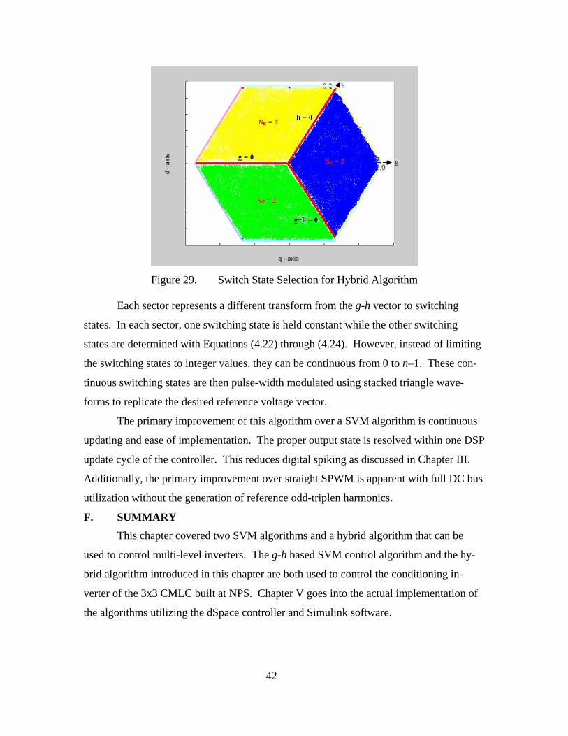
Figure 29. Switch State Selection for Hybrid Algorithm
Each sector represents a different transform from the g-h vector to switching
states. In each sector, one switching state is held constant while the other switching
states are determined with Equations (4.22) through (4.24). However, instead of limiting
the switching states to integer values, they can be continuous from 0 to n–1. These con-
tinuous switching states are then pulse-width modulated using stacked triangle wave-
forms to replicate the desired reference voltage vector.
The primary improvement of this algorithm over a SVM algorithm is continuous
updating and ease of implementation. The proper output state is resolved within one DSP
update cycle of the controller. This reduces digital spiking as discussed in Chapter III.
Additionally, the primary improvement over straight SPWM is apparent with full DC bus
utilization without the generation of reference odd-triplen harmonics.
F. SUMMARY
This chapter covered two SVM algorithms and a hybrid algorithm that can be
used to control multi-level inverters. The g-h based SVM control algorithm and the hy-
brid algorithm introduced in this chapter are both used to control the conditioning in-
verter of the 3x3 CMLC built at NPS. Chapter V goes into the actual implementation of
the algorithms utilizing the dSpace controller and Simulink software.
42
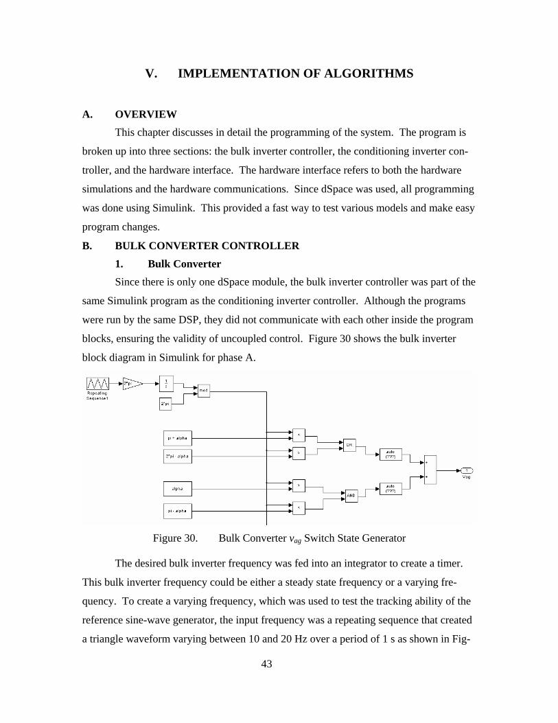
V. IMPLEMENTATION OF ALGORITHMS
A. OVERVIEW
This chapter discusses in detail the programming of the system. The program is
broken up into three sections: the bulk inverter controller, the conditioning inverter con-
troller, and the hardware interface. The hardware interface refers to both the hardware
simulations and the hardware communications. Since dSpace was used, all programming
was done using Simulink. This provided a fast way to test various models and make easy
program changes.
B. BULK CONVERTER CONTROLLER
1. Bulk Converter
Since there is only one dSpace module, the bulk inverter controller was part of the
same Simulink program as the conditioning inverter controller. Although the programs
were run by the same DSP, they did not communicate with each other inside the program
blocks, ensuring the validity of uncoupled control. Figure 30 shows the bulk inverter
block diagram in Simulink for phase A.
Figure 30. Bulk Converter vag Switch State Generator
The desired bulk inverter frequency was fed into an integrator to create a timer.
This bulk inverter frequency could be either a steady state frequency or a varying fre-
quency. To create a varying frequency, which was used to test the tracking ability of the
reference sine-wave generator, the input frequency was a repeating sequence that created
a triangle waveform varying between 10 and 20 Hz over a period of 1 s as shown in Fig-
43
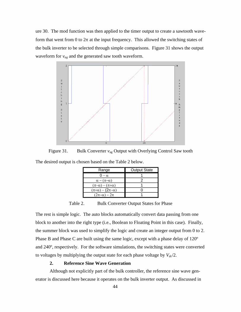
ure 30. The mod function was then applied to the timer output to create a sawtooth wave-
form that went from 0 to 2π at the input frequency. This allowed the switching states of
the bulk inverter to be selected through simple comparisons. Figure 31 shows the output
waveform for vag and the generated saw tooth waveform.
Figure 31. Bulk Converter vag Output with Overlying Control Saw tooth
The desired output is chosen based on the Table 2 below.
Range Output State0 − α 1
α − (π−α) 2(π−α) − (π+α) 1
(π+α) − (2π−α) 0(2π−α) − 2π 1
Table 2. Bulk Converter Output States for Phase
The rest is simple logic. The auto blocks automatically convert data passing from one
block to another into the right type (i.e., Boolean to Floating Point in this case). Finally,
the summer block was used to simplify the logic and create an integer output from 0 to 2.
Phase B and Phase C are built using the same logic, except with a phase delay of 120º
and 240º, respectively. For the software simulations, the switching states were converted
to voltages by multiplying the output state for each phase voltage by Vdc/2.
2. Reference Sine Wave Generation Although not explicitly part of the bulk controller, the reference sine wave gen-
erator is discussed here because it operates on the bulk inverter output. As discussed in 44

Chapter II, generating the reference sine wave from the bulk inverter is key to operating
the CMLC as an uncoupled system. Instead of filtering the bulk inverter output, an inte-
grator was used to time specific switching states. The time t was then used to calculate
the frequency. By doing this, the reference sine wave frequency can be updated up to
twelve times during a single bulk inverter period. By updating the frequency more often,
better dynamic response is gained. However, this also leads to less accurate calculations
because the error of the calculations increase when shorter output states are timed. Con-
versely, the error can be reduced by either updating the frequency less often, resulting in
longer timed sections, or by using a faster DSP. In order to try to maximize the response,
and minimize the error of the calculations, the reference sine wave frequency was up-
dated six times in one period for this thesis, twice per phase as shown in Figure 32.
Figure 32. Frequency Calculation
The above figure is only for vab but is identical for vbc and vca. First, the absolute
value of the normalized line-to-line voltage is found, creating the waveform shown in
Figure 33.
45

Figure 33. Absolute Value of Normalized Line-to-Line Voltage
The next step detects a rising and falling edge at a value of 0.7. The value of 0.7 was
chosen to prevent noise from triggering the edge detectors. At this point, the rising edge
detector resets the integrator and starts timing the bulk inverter output state. The falling
edge detector acts as a trigger to a sample-and-hold block. This block captures the fre-
quency calculated by Equation (3.8). There is one additional block; this is a single- cycle
delay. It was found that the sample-and-hold trigger would capture the frequency value a
cycle too late. This resulted in an erroneous frequency, thus the single cycle delay was
added.
The falling edge detector for vab is also used to reset a counter which keeps track
of the phase (A, B or C) providing the frequency. The remaining two falling edge detec-
tors (on the other line-to-line voltages) act as a clock for the counter. Figure 34 shows
the counter and multiport switch that select the most up-to-date calculated frequency.
46

Figure 34. Frequency Selection
The counter is reset with a falling edge of phase A. This sets the output to zero,
which corresponds to the first input of the multiport switch. Next the phase B detector
triggers, which sets the counter output to “1”, and selects the phase B calculated fre-
quency. This process repeats for phase C, and then resets with the second falling edge of
phase A. Calculating the frequency for a single phase multiple times would have been a
simpler implementation. However, with a slow DSP, the frequency calculations for
shorter output states (Vab/Vdc = 0.5 or 0) would not be as accurate. Optionally, the sys-
tem could be set up to update the frequency three times per cycle, once per phase. This
option would result in a better steady-state response due to longer timed states (less error
in the calculations), but less dynamic response due to fewer frequency updates. To mini-
mize the error and maximize the dynamic response, the frequency was updated six times
per cycle.
With the frequencies calculated, the final step is generating the sine wave and put-
ting it in phase with the bulk converter waveform. This is illustrated in Figure 35.
47
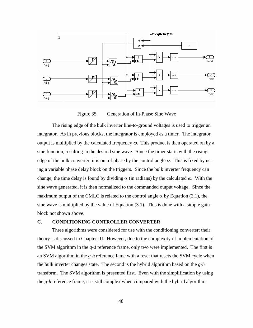
Figure 35. Generation of In-Phase Sine Wave
The rising edge of the bulk inverter line-to-ground voltages is used to trigger an
integrator. As in previous blocks, the integrator is employed as a timer. The integrator
output is multiplied by the calculated frequency ω. This product is then operated on by a
sine function, resulting in the desired sine wave. Since the timer starts with the rising
edge of the bulk converter, it is out of phase by the control angle α. This is fixed by us-
ing a variable phase delay block on the triggers. Since the bulk inverter frequency can
change, the time delay is found by dividing α (in radians) by the calculated ω. With the
sine wave generated, it is then normalized to the commanded output voltage. Since the
maximum output of the CMLC is related to the control angle α by Equation (3.1), the
sine wave is multiplied by the value of Equation (3.1). This is done with a simple gain
block not shown above.
C. CONDITIONING CONTROLLER CONVERTER Three algorithms were considered for use with the conditioning converter; their
theory is discussed in Chapter III. However, due to the complexity of implementation of
the SVM algorithm in the q-d reference frame, only two were implemented. The first is
an SVM algorithm in the g-h reference fame with a reset that resets the SVM cycle when
the bulk inverter changes state. The second is the hybrid algorithm based on the g-h
transform. The SVM algorithm is presented first. Even with the simplification by using
the g-h reference frame, it is still complex when compared with the hybrid algorithm.
48

1. SVM Algorithm Since both algorithms use the g-h transform, the transform block is only presented
in this section. Chapter III discussed the transform in detail, but the implementation is
slightly different since both the bulk inverter output voltages and the reference sine
waves were normalized to Vdc. Figure 36 shows the transform.
Figure 36. g-h Reference Frame Transform
The commanded voltage for the conditioning converter was found by [2]
* * , *g g f xv v v− = (5.1)
where v*g is the bulk inverter phase voltage , v*g,f is the reference sine wave, and v*x is the
conditioning inverter commanded phase voltage. Once the commanded phase voltages
are known, the voltages are then converted into line-to-line voltages. With the com-
manded voltages in line-to-line terms, they are then transformed according to Equations
(4.7) and (4.8) to find the g-h values. An additional gain of two was necessary since the
line-to-ground voltages were used vice the line-to-neutral voltages. Finally, Vgx and Vdx
are used as the commanded inputs for the conditioning inverter SVM and hybrid algo-
rithms.
The next block is the software reset block, which was used to demonstrate the
ability to reduce the digital spiking. Ideally, an edge detector circuit tied to the bulk in-
verter outputs would be used as the reset signal. Since an edge detector circuit was not
readily available, a software-reset block was created to validate the concept. Figure 37
shows the software interrupt block.
49

Figure 37. Software-Reset Block
To create the reset signal, the normalized bulk inverter outputs were ran through
comparators set to detect output voltage changes. The comparator outputs were then
summed together and run through a derivative block. The derivative block creates a digi-
tal pulse for each change in voltage. The output of the derivative is limited to between 0
and 1. This signal is then used to reset the SVM cycle when the bulk inverter changes
state.
With the basics done, the next step involved the actual SVM algorithm, which
starts with the detection of the three nearest vectors. This is done exactly as it was shown
in Equations (4.9) through (4.13). Figure 38 shows the Simulink code for detecting the
vectors.
50

Figure 38. Three Nearest Vector Detection
There are four outputs: Vul_out, Vlu_out, Vuu_Vll, and 1_Vuu. Vul_out and Vlu_out are
self-explanatory and represent two of the three nearest vectors. Vuu_Vll is either the Vuu
or Vll vector depending on the sign of Equation (4.14). The 1_Vuu output holds a value of
“1” if the Vuu_Vll vector is Vuu, and a value of “0” when the Vuu_Vll vector is Vll. This is
important for the duty cycle calculations. If the value is “1”, Equations (4.18) through
(4.20) are used to calculate duty cycles, otherwise, Equations (4.15) through (4.17) are
used. Figure 39 shows the code for calculating the duty cycles.
51

Figure 39. Calculation of Duty Cycles
Once again, the Simulink blocks were programmed to precisely follow the equa-
tions. The duty cycle is output as a vector of [dul dlu dll_duu]T. It is important to note that
these duty cycle calculations are continuously updated at the DSP update rate, and not the
SVM frequency. This fact, in conjunction, with the reset allows a near instantaneous
change in the conditioning inverter output when the bulk inverter switches state.
In order for SVM to work, the duty cycle vector and the output vectors must be
held constant for the duration of the SVM period. This is accomplished by utilizing two
triggered output blocks as shown in Figure 40a and Figure 40b. Figure 40a is the vector
hold block and Figure 40b is the duty cycle hold block.
(a) (b)
Figure 40. (a) Vector Hold Block and (b) Duty Cycle Hold Block
52
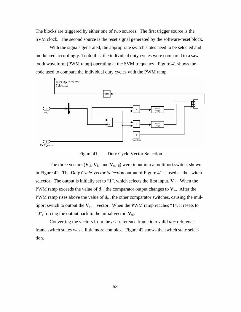
The blocks are triggered by either one of two sources. The first trigger source is the
SVM clock. The second source is the reset signal generated by the software-reset block.
With the signals generated, the appropriate switch states need to be selected and
modulated accordingly. To do this, the individual duty cycles were compared to a saw
tooth waveform (PWM ramp) operating at the SVM frequency. Figure 41 shows the
code used to compare the individual duty cycles with the PWM ramp.
Figure 41. Duty Cycle Vector Selection
The three vectors (Vul, Vlu, and Vuu_ll) were input into a multiport switch, shown
in Figure 42. The Duty Cycle Vector Selection output of Figure 41 is used as the switch
selector. The output is initially set to “1”, which selects the first input, Vul. When the
PWM ramp exceeds the value of dul, the comparator output changes to Vlu. After the
PWM ramp rises above the value of dlu, the other comparator switches, causing the mul-
tiport switch to output the Vuu_ll vector. When the PWM ramp reaches “1”, it resets to
“0”, forcing the output back to the initial vector, Vul.
Converting the vectors from the g-h reference frame into valid abc reference
frame switch states was a little more complex. Figure 42 shows the switch state selec-
tion.
53
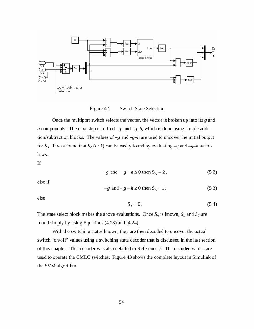
Figure 42. Switch State Selection
Once the multiport switch selects the vector, the vector is broken up into its g and
h components. The next step is to find –g, and –g–h, which is done using simple addi-
tion/subtraction blocks. The values of –g and –g–h are used to uncover the initial output
for SA. It was found that SA (or k) can be easily found by evaluating –g and –g–h as fol-
lows.
If
Aand 0 then S 2g g h− − − ≤ = , (5.2)
else if Aand 0 then S 1g g h− − − ≥ = , (5.3)
else AS 0= . (5.4)
The state select block makes the above evaluations. Once SA is known, SB and SC are
found simply by using Equations (4.23) and (4.24).
With the switching states known, they are then decoded to uncover the actual
switch “on/off” values using a switching state decoder that is discussed in the last section
of this chapter. This decoder was also detailed in Reference 7. The decoded values are
used to operate the CMLC switches. Figure 43 shows the complete layout in Simulink of
the SVM algorithm.
54
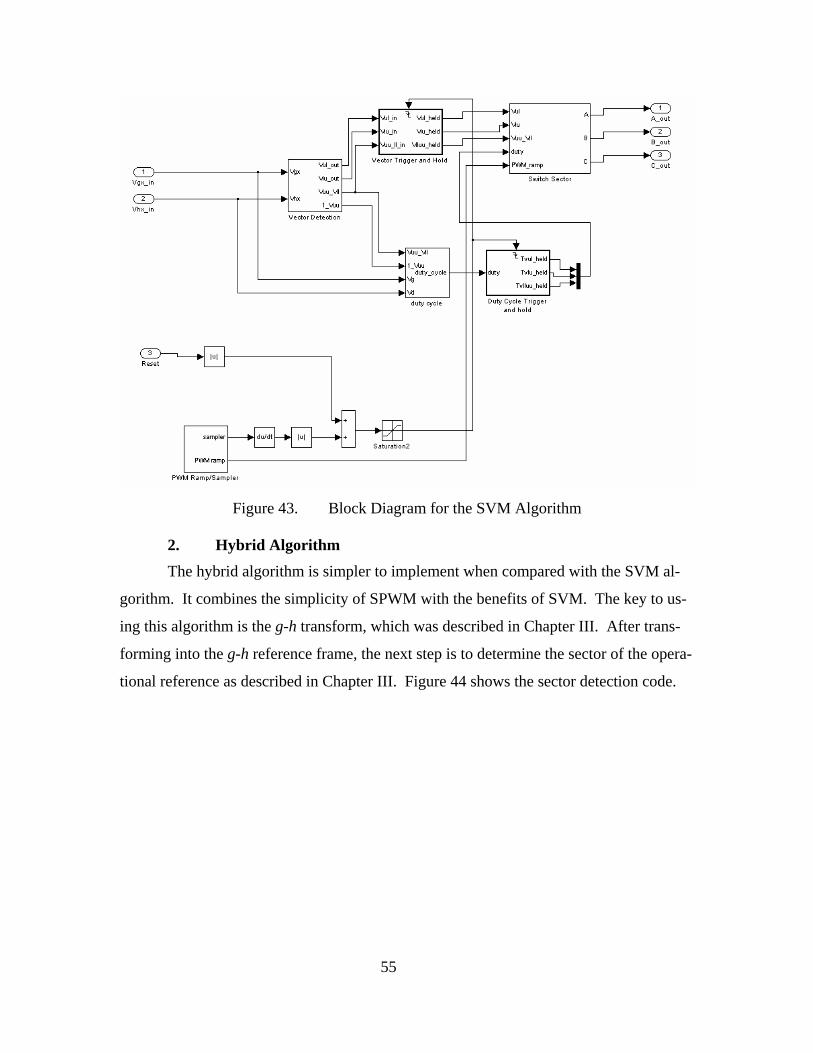
Figure 43. Block Diagram for the SVM Algorithm
2. Hybrid Algorithm The hybrid algorithm is simpler to implement when compared with the SVM al-
gorithm. It combines the simplicity of SPWM with the benefits of SVM. The key to us-
ing this algorithm is the g-h transform, which was described in Chapter III. After trans-
forming into the g-h reference frame, the next step is to determine the sector of the opera-
tional reference as described in Chapter III. Figure 44 shows the sector detection code.
55

Figure 44. Sector Selection
This is an easy evaluation since the three line equations are g = 0, h = 0, and g+h
= 0. By comparing the reference vector with these equations, the sector can be deter-
mined. Depending on the sector, one of the outputs (A_Enable, B_Enable, or C_Enable)
is set to one.
With the enables determined, the next step is finding the analog values of the
switching states. Figure 45 shows the layout for determining the analog switching states.
56

Figure 45. Hybrid Algorithm
The analog switching states are created by setting each switch to two, and then calculat-
ing the others using Equations (4.22) through (4.24). The enables from Figure 44 only
allow one set of the switching states to the outputs, A1, B1, and C1. These values are
then utilized for the PWM, as shown in Figure 46.
57

Figure 46. Hybrid Algorithm Pulse Width Modulation
The outputs, A1, B1, and C1 are then PWM using triangular waveforms as was
done for the SPWM technique discussed in Chapter II. This PWM output is then fed into
the switching state decoder blocks discussed later in this chapter. The decoded values are
used to operate the CMLC switches.
D. HARDWARE INTERFACE
1. Hardware Communications
In order to implement the two algorithms, the bulk inverter output voltages and
the DC bus voltage had to be read in. The bus voltage Vdc was needed for two things.
First, Vdc is used to normalize the bulk converter phase voltages, vag, vbg, and vcg. Second,
Vdc is important for implementing capacitor voltage-balancing strategies and eliminating
the secondary power supply. Neither capacitor voltage balancing nor secondary power
supply elimination was done in this thesis, but will be implemented in a follow-on thesis.
dSpace provides its own toolbox of Simulink tools. This made it simple to read in
the analog voltages from the dSpace DSP I/O Board. Figure 47 shows the dSpace Simu-
link A/D communication blocks.
58
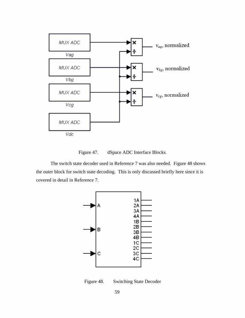
Figure 47. dSpace ADC Interface Blocks.
The switch state decoder used in Reference 7 was also needed. Figure 48 shows
the outer block for switch state decoding. This is only discussed briefly here since it is
covered in detail in Reference 7.
Figure 48. Switching State Decoder
59

The inputs, A, B, and C, correspond to the three phases of the system. Since the
switching state decoder block was designed for the NPS 3x3 CMLC, the inputs accept
values of “0”, “1”, or “2”. This block takes the three inputs, and decodes them into actual
switch on/off states. Because there are four switches per phase per converter, there are
four outputs per phase. These outputs are either “1” or “0”, corresponding to “on” or
“off”. Table 1 of Chapter I shows the relation between switching states and switch values
for a nine-level inverter. Table 3 below shows the relation between switching state and
switch values for a single converter phase of the NPS 3x3 CMLC.
State Switch 1 Switch 2 Switch 3 Switch 4
0 0 0 1 11 0 1 1 02 1 1 0 0
Table 3. Switching State Decoder Table With the switching states decoded into binary, they were then output through the
dSpace I/O board. Fortunately, dSpace provided a block to communicate with the digital
I/O board. Figure 49 shows the dSpace block used.
Figure 49. Phase A Switch Interface for Bulk and Conditioning Inverter.
60
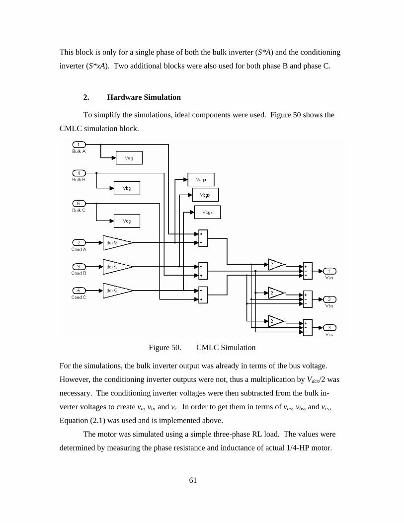
61
This block is only for a single phase of both the bulk inverter (S*A) and the conditioning
inverte xA) were also used for both phase B and phase C.
Simulation
To simplify the simulations, ideal components were used. Figure 50 shows the
CMLC simulation block.
r (S* . Two additional blocks
2. Hardware
Figure 50. CMLC Simulation
For the simulations, the bulk inverter output was already in terms of the bus voltage.
However, the conditioning inverter outputs were not, thus a multiplication by Vdcx/2 wa
necessary. The conditioning inverter voltages were t
s
hen subtracted from the bulk in-
verter v
actual 1/4-HP motor.
oltages to create va, vb, and vc. In order to get them in terms of vas, vbs, and vcs,
Equation (2.1) was used and is implemented above.
The motor was simulated using a simple three-phase RL load. The values were
determined by measuring the phase resistance and inductance of

62
he measured resistance and inductance were 12 Ω and 6.6 mH, respectively. This mo-
r modeling simplification made algorithm verification easier.
e models and then
download them into the DSP card. The dSpace HIL system made control strategy
changes easy via quick program modifications rather than hardware changes. Chapter VI
utilizes this code to do both simulations and run hardware tests.
T
to
E. SUMMARY
This chapter covered the coding necessary to run the algorithms. dSpace greatly
simplified the coding by allowing the use of Simulink to create th

63
VI. RESULTS
A. OVERVIEW
Prior to testing the actual 3x3 CMLC hardware, simulations of the hardware were
used to fine-tune the control algorithms. The uncoupled control algorithms, along with
the ideal model of the CMLC with motor load (a series connected 6.6-mH inductance and
12-Ω resistance) were simulated in Simulink. The ideal model is laid out in Chapter V.
Results were evaluated using Matlab. The evaluation criteria consisted of the THD of the
output current and voltage, and the spike width observed in the voltage.
After the initial simulations, the system was then tested with the actual hardware
built at NPS. The CMLC was used to power a 1/4-HP (208 Vll, 1.2 A), 3-phase, wye-
connected, 60-Hz induction motor. The motor was initially operated at 10 Hz and no
load. The algorithms were tested with a DSP update frequency of 18 kHz, and a switch-
ing frequency of 3.6 kHz. In order to test the tracking ability of the reference sine wave
generation, the bulk inverter frequency was varied from to 10 to 20 Hz. Final testing in-
volved comparing the previously developed, joint controlled SPWM algorithm against
the uncoupled controller using the hybrid algorithm developed in this thesis for the condi-
tioning inverter. The comparison testing was done operating the motor at 60 Hz, under
full load (1/4 HP). The hybrid algorithm was chosen due to its implementation simplic-
ity. Since the algorithm required less calculations then the original, the DSP update fre-
quency could be increased to improve results. The operating frequency of the motor was
increased six fold (from the initial starting point of 10 Hz). This required the DSP update
frequency to be increased for like comparisons. However, the DSP update frequency
could only be increased to 30 kHz, the limit of the 20-MHz DSP card with the uncoupled
controller programming. To further improve results the switching frequency was in-
creased to 7.2 kHz. This provided results comparable with the 10 Hz tests. Measure-
ments for the hardware tests were obtained using the Tektronix TDS3012B digital oscil-
loscope and the HP3561A spectrum analyzer.

B. SIMULATIONS The algorithms and hardware model were programmed in Simulink. Figure 51
below shows the overall Simulink block diagram for the entire system with load. For a
detailed description of the blocks, please refer to Chapter V.
Figure 51. Simulated System
1. SVM Simulations Figures 52 and 53 depict the output current with frequency spectrum and a blow-
up view of the transition spike for the conditioning inverter using the SVM algorithm
without the reset. The first 60 harmonics are contained in Figure 52.
64
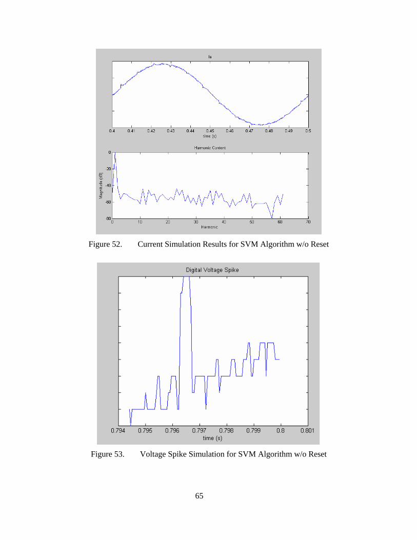
Figure 52. Current Simulation Results for SVM Algorithm w/o Reset
Figure 53. Voltage Spike Simulation for SVM Algorithm w/o Reset
65

The calculated THD using Matlab was 1.97% for the first 60 harmonics. The
spike width was measured to be 480 µs. These measurements are used as a basis of com-
parison for the other algorithms.
The next set of simulations was done for the system with the conditioning inverter
controlled by the SVM algorithm using the reset to reduce spike width. Figures 54 and
55 below show the current waveform with THD and the voltage spike width, respec-
tively.
Figure 54. Current Simulation Results for SVM Algorithm with Interrupt
66
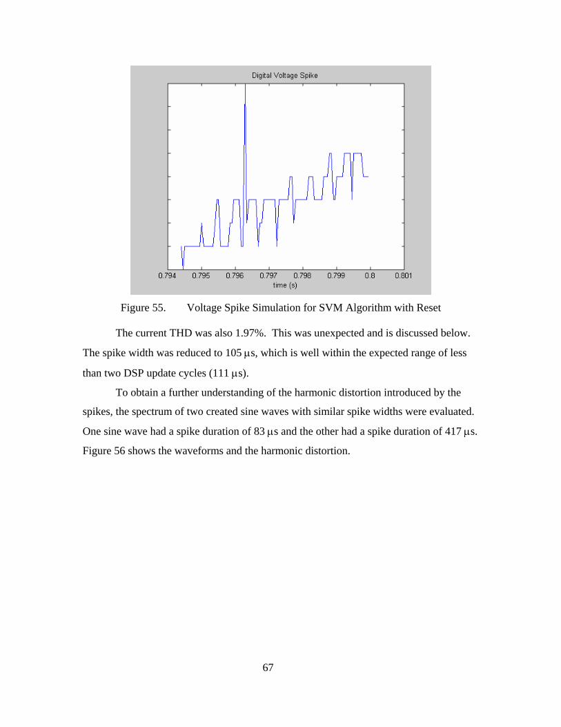
Figure 55. Voltage Spike Simulation for SVM Algorithm with Reset
The current THD was also 1.97%. This was unexpected and is discussed below.
The spike width was reduced to 105 µs, which is well within the expected range of less
than two DSP update cycles (111 µs).
To obtain a further understanding of the harmonic distortion introduced by the
spikes, the spectrum of two created sine waves with similar spike widths were evaluated.
One sine wave had a spike duration of 83 µs and the other had a spike duration of 417 µs.
Figure 56 shows the waveforms and the harmonic distortion.
67

Figure 56. Harmonic Distortion for Different Spike Widths
The THD for the narrow spike is 0.45% while the wide spike THD is 2.16%.
This suggests that there should be some difference in the THD between the two algo-
rithms.
With this known, further simulations were run to determine the error in THD cal-
culations. The problem appeared to be a resolution issue. Therefore, the simulations
were rerun with a step size 10 times smaller than the original 55.6 µs. This new ar-
rangement required a phase delay on the reset to ensure it operated at 55.6 µs (the time
delay that it would operate for hardware tests) verses 5.6 µs. The corrected THD meas-
urement for the SVM algorithm without reset is 1.34% resulting in a 31% decrease.
2. Hybrid Algorithm Simulations Next, the hybrid algorithm developed in Chapter III was evaluated. Figure 57
shows the current waveform with the harmonic content through the first 60 harmonics for
the hybrid algorithm.
68
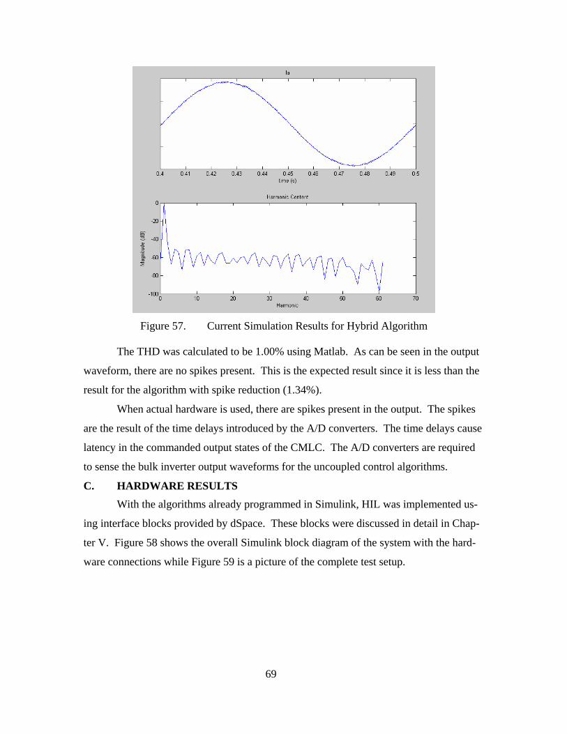
Figure 57. Current Simulation Results for Hybrid Algorithm
The THD was calculated to be 1.00% using Matlab. As can be seen in the output
waveform, there are no spikes present. This is the expected result since it is less than the
result for the algorithm with spike reduction (1.34%).
When actual hardware is used, there are spikes present in the output. The spikes
are the result of the time delays introduced by the A/D converters. The time delays cause
latency in the commanded output states of the CMLC. The A/D converters are required
to sense the bulk inverter output waveforms for the uncoupled control algorithms.
C. HARDWARE RESULTS
With the algorithms already programmed in Simulink, HIL was implemented us-
ing interface blocks provided by dSpace. These blocks were discussed in detail in Chap-
ter V. Figure 58 shows the overall Simulink block diagram of the system with the hard-
ware connections while Figure 59 is a picture of the complete test setup.
69

Figure 58. Complete System with Hardware Connections
Figure 59. Hardware Test Setup.
70
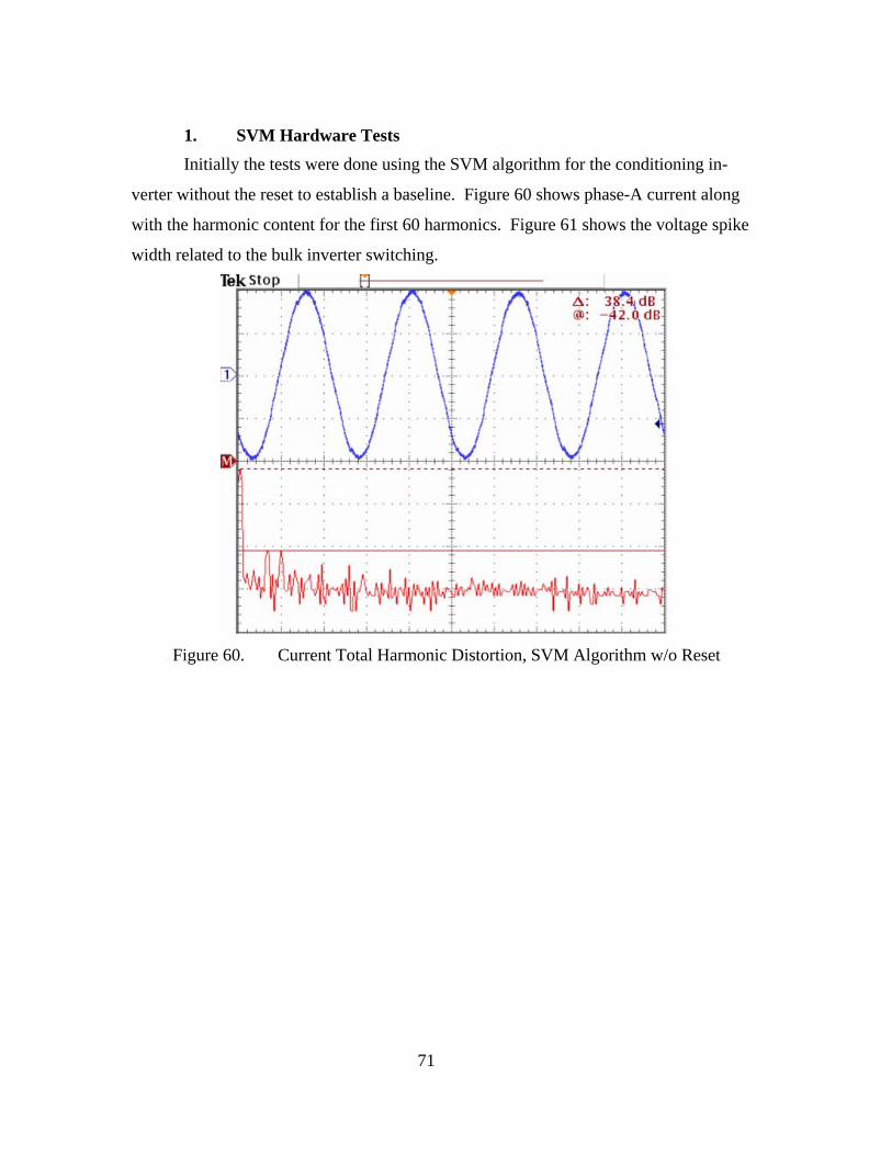
1. SVM Hardware Tests Initially the tests were done using the SVM algorithm for the conditioning in-
verter without the reset to establish a baseline. Figure 60 shows phase-A current along
with the harmonic content for the first 60 harmonics. Figure 61 shows the voltage spike
width related to the bulk inverter switching.
Figure 60. Current Total Harmonic Distortion, SVM Algorithm w/o Reset
71
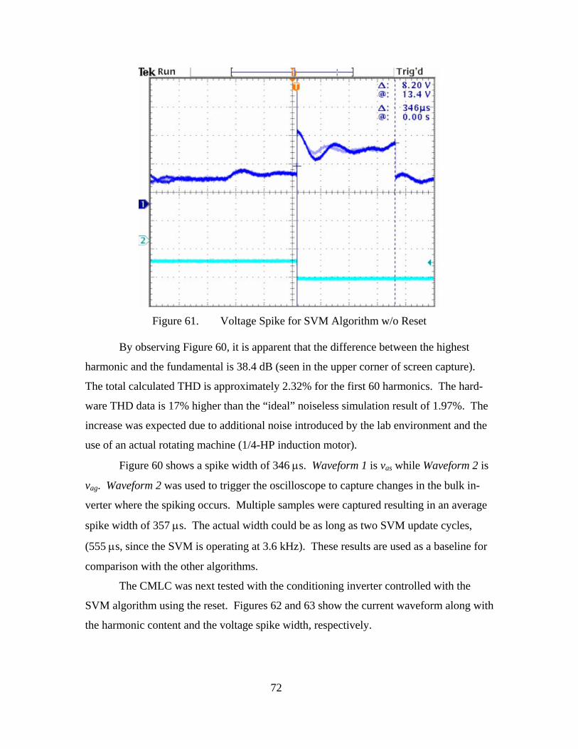
Figure 61. Voltage Spike for SVM Algorithm w/o Reset
By observing Figure 60, it is apparent that the difference between the highest
harmonic and the fundamental is 38.4 dB (seen in the upper corner of screen capture).
The total calculated THD is approximately 2.32% for the first 60 harmonics. The hard-
ware THD data is 17% higher than the “ideal” noiseless simulation result of 1.97%. The
increase was expected due to additional noise introduced by the lab environment and the
use of an actual rotating machine (1/4-HP induction motor).
Figure 60 shows a spike width of 346 µs. Waveform 1 is vas while Waveform 2 is
vag. Waveform 2 was used to trigger the oscilloscope to capture changes in the bulk in-
verter where the spiking occurs. Multiple samples were captured resulting in an average
spike width of 357 µs. The actual width could be as long as two SVM update cycles,
(555 µs, since the SVM is operating at 3.6 kHz). These results are used as a baseline for
comparison with the other algorithms.
The CMLC was next tested with the conditioning inverter controlled with the
SVM algorithm using the reset. Figures 62 and 63 show the current waveform along with
the harmonic content and the voltage spike width, respectively.
72
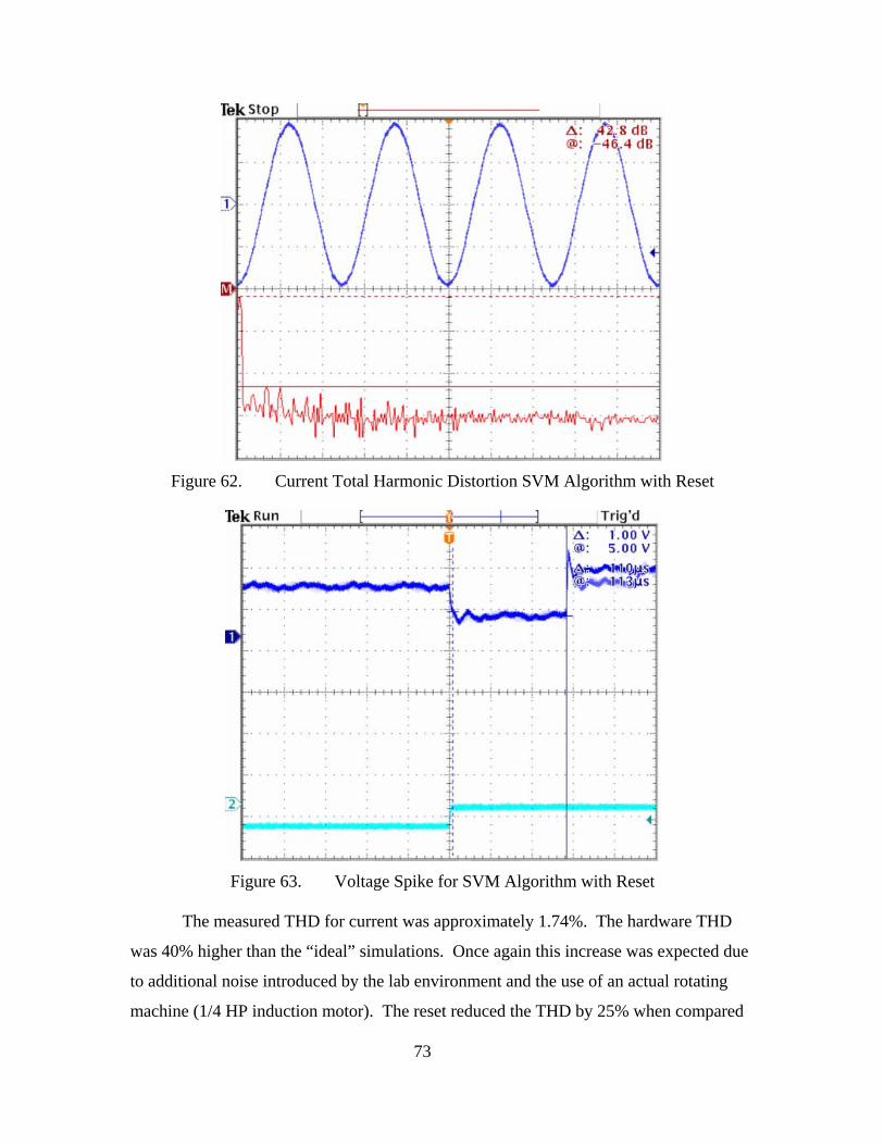
Figure 62. Current Total Harmonic Distortion SVM Algorithm with Reset
Figure 63. Voltage Spike for SVM Algorithm with Reset
The measured THD for current was approximately 1.74%. The hardware THD
was 40% higher than the “ideal” simulations. Once again this increase was expected due
to additional noise introduced by the lab environment and the use of an actual rotating
machine (1/4 HP induction motor). The reset reduced the THD by 25% when compared
73

to the SVM algorithm without the reset. This matched to within 20% of the 31% de-
crease in THD between the two algorithms for the simulation. Figure 63 shows that the
spike width was reduced to 110 µs, slightly higher than the simulations, but still less than
two DSP update cycles (111 µs).
2. Hybrid Algorithm Hardware Results After the testing of the SVM algorithms, the system was tested with the hybrid al-
gorithm controlling the conditioning inverter. Figure 64 shows the current waveform
with the harmonic content through the first 60 harmonics, and Figure 65 shows the spike
width.
Figure 64. Current THD for the Hybrid Algorithm
74
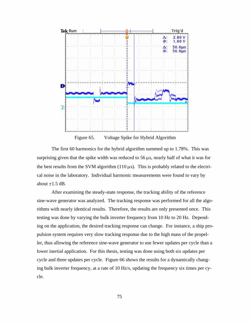
Figure 65. Voltage Spike for Hybrid Algorithm
The first 60 harmonics for the hybrid algorithm summed up to 1.78%. This was
surprising given that the spike width was reduced to 56 µs, nearly half of what it was for
the best results from the SVM algorithm (110 µs). This is probably related to the electri-
cal noise in the laboratory. Individual harmonic measurements were found to vary by
about ±1.5 dB.
After examining the steady-state response, the tracking ability of the reference
sine-wave generator was analyzed. The tracking response was performed for all the algo-
rithms with nearly identical results. Therefore, the results are only presented once. This
testing was done by varying the bulk inverter frequency from 10 Hz to 20 Hz. Depend-
ing on the application, the desired tracking response can change. For instance, a ship pro-
pulsion system requires very slow tracking response due to the high mass of the propel-
ler, thus allowing the reference sine-wave generator to use fewer updates per cycle than a
lower inertial application. For this thesis, testing was done using both six updates per
cycle and three updates per cycle. Figure 66 shows the results for a dynamically chang-
ing bulk inverter frequency, at a rate of 10 Hz/s, updating the frequency six times per cy-
cle.
75

Figure 66. IA Dynamic Response Hybrid Algorithm
Due to the changing frequency of the sine wave, THD measurements were not
appropriate. However, Figure 66 does show little to no additional distortion introduced
in the sine wave due to the varying frequency. This suggests that the reference sine wave
generator is tracking the bulk inverter frequency accurately.
D. COMPARISON WITH SPWM ALGORITHM
A final test was done comparing the uncoupled controlled CMLC (utilizing the
hybrid algorithm to control the conditioning inverter) with the jointly controlled CMLC
(using the SPWM algorithm developed in Reference 7). The tests were run at 60 Hz (or
rated motor speed), with the motor operating at full load (of 1/4 HP). Furthermore, only
the first 20 harmonics were used to measure THD. The first 20 harmonics were used to
allow a direct comparison to the results for the joint controller achieved in Reference 7.
Since the testing was done under load, the rated motor frequency was used. The increase
in frequency from 10 Hz decreased the performance of the uncoupled controller. Since
the frequency was increased six-fold, the error associated with the reference frequency
calculations also increased six-fold. To reduce the error, the system was operated at a
higher DSP update rate. This higher rate was possible due to the fewer number of calcu-
lations required by the hybrid algorithm compared to the SVM algorithm. To help fur-
ther increase the DSP update rate, the frequency calculations were only updated three
times per cycle instead of six times per cycle as in previous tests. The update rate was
increased from 18 kHz to 30 kHz. Lastly, the switching frequency was increased to 7.2
76
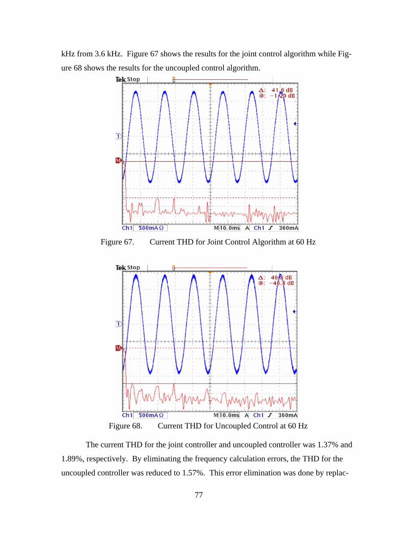
kHz from 3.6 kHz. Figure 67 shows the results for the joint control algorithm while Fig-
ure 68 shows the results for the uncoupled control algorithm.
Figure 67. Current THD for Joint Control Algorithm at 60 Hz
Figure 68. Current THD for Uncoupled Control at 60 Hz
The current THD for the joint controller and uncoupled controller was 1.37% and
1.89%, respectively. By eliminating the frequency calculation errors, the THD for the
uncoupled controller was reduced to 1.57%. This error elimination was done by replac-
77
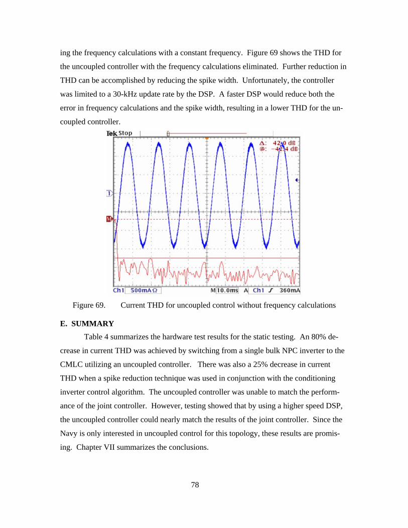
ing the frequency calculations with a constant frequency. Figure 69 shows the THD for
the uncoupled controller with the frequency calculations eliminated. Further reduction in
THD can be accomplished by reducing the spike width. Unfortunately, the controller
was limited to a 30-kHz update rate by the DSP. A faster DSP would reduce both the
error in frequency calculations and the spike width, resulting in a lower THD for the un-
coupled controller.
Figure 69. Current THD for uncoupled control without frequency calculations
E. SUMMARY
Table 4 summarizes the hardware test results for the static testing. An 80% de-
crease in current THD was achieved by switching from a single bulk NPC inverter to the
CMLC utilizing an uncoupled controller. There was also a 25% decrease in current
THD when a spike reduction technique was used in conjunction with the conditioning
inverter control algorithm. The uncoupled controller was unable to match the perform-
ance of the joint controller. However, testing showed that by using a higher speed DSP,
the uncoupled controller could nearly match the results of the joint controller. Since the
Navy is only interested in uncoupled control for this topology, these results are promis-
ing. Chapter VII summarizes the conclusions.
78

Algorithm Current THD Voltage THD
Bulk Converter (alone) 8.28% 15.18%
Uncoupled Control: SVM algorithm w/o reset (10 Hz) 2.32% 5.93%
Uncoupled Control: CMLC SVM algorithm with reset (10 Hz) 1.74% 4.30%
Uncoupled Control: Hybrid algorithm (10 Hz) 1.78% 4.36%
Joint Control: SPWM (60 Hz, 20 harmonics) 1.37%
Uncoupled Control: Hybrid algorithm (60 Hz, 20 harmonics) 1.89%
Uncoupled Control: Hybrid algorithm (no frequency errors) 1.57%
Table 4. Summarized Hardware Test Results
79

80
THIS PAGE INTENTIONNALY LEFT BLANK
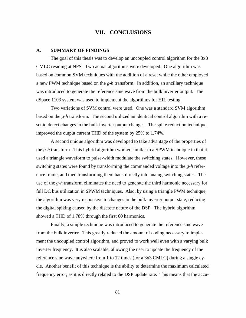
81
VII. CONCLUSIONS
A. SUMMARY OF FINDINGS
The goal of this thesis was to develop an uncoupled control algorithm for the 3x3
CMLC residing at NPS. Two actual algorithms were developed. One algorithm was
based on common SVM techniques with the addition of a reset while the other employed
a new PWM technique based on the g-h transform. In addition, an ancillary technique
was introduced to generate the reference sine wave from the bulk inverter output. The
dSpace 1103 system was used to implement the algorithms for HIL testing.
Two variations of SVM control were used. One was a standard SVM algorithm
based on the g-h transform. The second utilized an identical control algorithm with a re-
set to detect changes in the bulk inverter output changes. The spike reduction technique
improved the output current THD of the system by 25% to 1.74%.
A second unique algorithm was developed to take advantage of the properties of
the g-h transform. This hybrid algorithm worked similar to a SPWM technique in that it
used a triangle waveform to pulse-width modulate the switching states. However, these
switching states were found by transforming the commanded voltage into the g-h refer-
ence frame, and then transforming them back directly into analog switching states. The
use of the g-h transform eliminates the need to generate the third harmonic necessary for
full DC bus utilization in SPWM techniques. Also, by using a triangle PWM technique,
the algorithm was very responsive to changes in the bulk inverter output state, reducing
the digital spiking caused by the discrete nature of the DSP. The hybrid algorithm
showed a THD of 1.78% through the first 60 harmonics.
Finally, a simple technique was introduced to generate the reference sine wave
from the bulk inverter. This greatly reduced the amount of coding necessary to imple-
ment the uncoupled control algorithm, and proved to work well even with a varying bulk
inverter frequency. It is also scalable, allowing the user to update the frequency of the
reference sine wave anywhere from 1 to 12 times (for a 3x3 CMLC) during a single cy-
cle. Another benefit of this technique is the ability to determine the maximum calculated
frequency error, as it is directly related to the DSP update rate. This means that the accu-

82
racy improves with the speed of the DSP or the reduction in commanded output fre-
quency.
The research conducted for this thesis is beneficial for future naval development
of the All-Electric Ship. As the need for higher power high fidelity drives increases, the
CMLC with uncoupled control offers significant benefits over existing topologies. These
improvements include:
• high power density and low cost due to the use of a COTS bulk converter
with no modifications,
• high fidelity due to the use of a small specially designed conditioning con-
verter, and
• high reliability due to system redundancy by having two converters.
B. FUTURE WORK The navy is moving towards the All-Electric Ship. In order to remain part of this
paradigm shift, NPS needs to expand research in the area of high-power, high-fidelity
drives. This includes further research into CMLC. Future research might include:
• removing the secondary power supply,
• constructing a high power CMLC,
• constructing a higher-level CMLC, and
• implementing algorithms on higher speed DSPs.
83
LIST OF REFERENCES
[1] Robert W. Ashton, Thomas H. Fikse, Joseph R. Sullivan, and Thong N. Ly, “An Assessment of Industry-Based High Power Electronic Modules for Naval Use,” Naval Surface Warfare Center, Carderock Division, Technical Report No. NSWCCD-984-TM-2003/24, 2003
[2] K. A. Corzine, M.W. Wielebski, F.Z. Peng, and J. Wang, “Control of Cascaded
Multi-Level Inverters,” Proc. IEEE Electric Machines and Drives Conference, Vol. 3, pp. 1549-1555, 2003.
[3] M. Collins, “DD(X) IPS revolution in shipboard power,” NAVSEA PEO-510 In-
ternal Presentation, February 2003. [4] Alstom, “Mermaid Pods,” [http://www.alstom.com/static/html/acom-
AGF_NavPage-NavPage_StandardLeft_1069324214761.html], last accessed March 2005.
[5] Tom Fiske, private conversation at Naval Postgraduate School Power Systems
Lab, 2 May 2005. [6] K.A. Corzine, “Operation and Design of Multilevel Inverters,” Developed for the
Office of Naval Research, December 2003. [7] Jacob L. Barlow, Hardware-In-The-Loop Control of a Cascaded Multi-LEVEL
Converter, Master’s thesis, Naval Postgraduate School, Monterey, California, 2003.
[8] R. Krishnan, Electric Motor Drives Modeling, Analysis, and Control, pp. 209-
212, Prentice Hall, Englewood Cliffs New Jersey, 2001. [9] Zhong Du, Leon M. Tolbert, and John N. Chiasson, “Modulation Extension Con-
trol for Multilevel Converters Using Triplen Harmonic Injection with Low Switching Frequency,” presented at the 2005 Applied Power and Electronics Con-ference, Austin, March 2005.
[10] Quiang Song, Wenhua liu, GanguiYan, and Yuanhua Chen, “DSP-Based Univer-sal Space Vector Modulator for Multilevel Voltage Source Inverters,” Proc. 29th Annual Conference of the IEEE, Vol. 2, pp 1727-1732, Nov. 2003.
[11] G. Carrara, S. Gardella, M. Marchessoni, R. Salutari, andG. Sciutto, “A new Mul-tilevel PWM Method: A theoretical analysis,” IEEE Trans. Power Electronics, Vol. 7, No. 3, pp. 497-505, July 1992.

84
[12] J. K. Steinke, “Control strategy for a three phase AC traction drive with a 3-level GTO PWM inverter,” Proc. IEEE Power Electronics Specialists Conference, Vol. 1, pp. 431-438, April 1988.
[13] DSPACE, “Solutions for Control,” Company Product Catalogue, 1997. [14] DSPACE, “DS1103 PPC Controller Board,” Company Technical Sheet, 2003. [15] DSPACE, “Connector and LED Panels for Single-Board Hardware,” Company
Technical Sheet, 2003. [16] United States Coast Guard, “USCGC Healy,” [http://www.uscg.mil/-
pacarea/healy], last accessed May 2005. [17] Nicola Celanovic, Space Vector Modulation and Control of Multilevel Convert-
ers, Ph. D. Dissertation, Virginia Polytech Institute, Blacksburg Virginia, 2000. [18] Xuan Hou, Yongdong Li, and Yongheng Liu, “A Novel General Space Vector
Modulation Algorithm for Multilevel Inverter Based on Imaginary Coordination,” Power Electronics and Drive Systems, Vol. 1, pp. 392-296, 2003.
[19] United States Navy, “Navy Fact File – Aircraft Carriers,” [http://www.chin-
fo.navy.mil/navpalib/ships/carriers/], last accessed March 2005. [20] T. Doyle, H. Stevens, and H. Robey, “An historical overview of Navy electric
drive,” Naval Symposium on Electric Machines, Newport Rhode Island, July, 1997.
[21] Electronics Academy, “Cycloconverters and Control of Induction Motor Part-I,”
[http://www.e-shikshalaya.com/cyclo_file/cyclo%28part8%29.htm], last accessed April 2005.
[22] D. Finney, “AC motor variable frequency drives-consideration of the most eco-
nomic and technically viable converter power circuits for drives above 500 kW,” Proc. IEEE Colloquium on Very High Power Converter Devices and Applica-tions, pp. 6/1-6/4, December 1988.

85
INITIAL DISTRIBUTION LIST
1. Defense Technical Information Center Ft. Belvoir, Virginia
2. Dudley Knox Library
Naval Postgraduate School Monterey, California
3. Chairman, Code EC Department of Electrical and Computer Engineering
Naval Postgraduate School Monterey, California
4. Robert Ashton, Code EC/Ah Department of Electrical and Computer Engineering
Naval Postgraduate School Monterey, California
5. Alexander Julian, Code EC/Ah
Department of Electrical and Computer Engineering Naval Postgraduate School
Monterey, California